

Page 1
DSC-F55V
SERVICE MANUAL
Level 2
Ver 1.0 2000. 06
On the SY-59 board
This service manual provides the information that is premised the circuit board
replacement service and not intended repair inside the SY-59 board.
Therefore, schematic diagram, printed wiring board and electrical parts list of
the SY-59 board are not shown.
The following pages are not shown.
Block diagram............................... Page 3-9 to 3-16
Schematic diagram....................... Page 4-9 to 4-34
Printed wiring board ..................... Page 4-35 to 4-36
Electrical parts list ........................ Page 6-8 to 6-14
E Model
Australian Model
Hong Kong Model
Chinese Model
Tourist Model
Japanese Model
This service manual contains information
for japanese model as well.
The above-described information is shown in service manual Level 3.
SPECIFICATIONS
System
Image device
1/1.8 type color CCD
Lens
f = 6.85 mm
(37 mm when converted into a
35 mm still camera)
F = 2.8
Exposure control
Automatic exposure
White balance
Automatic, Indoor, Outdoor,
Hold
Data system
Movie: MPEG1
Still: JPEG, GIF (in TEXT
mode), TIFF
Audio with still image:
MPEG1 (Monaural)
Recording medium
“Memory Stick”
Flash
Recommended recording
distance:
0.3m to 2.5m
Input and output
connector
A/V OUT (Monaural)
Minijack
Video: 1 Vp-p, 75Ω,
unbalanced, sync negative
Audio: 327 mV (at a 47 kΩ
load)
Output impedance: 2.2 k
Digital I/O (USB)
Special minijack
LCD screen
Used LCD panel
2 type TFT (Thin Film
Transistor active matrix) drive
Total number of dots
123 200 (560×220) dots
General
Used battery pack
NP-FS11
Power requirements
3.6 V
Ω
Power consumption
(during recording)
3.3 W
Operation temperature
0°C to 40°C
Storage temperature
–20°C to +60°C
Maximum dime nsions
Approx. 103×79×48 mm
(w/h/d)
Mass
Approx. 300 g (including
battery pack NP-FS11,
“Memory Stick,” lens cap,
etc.)
Built-in microphone
Electret condenser microphone
Built-in speaker
Dynamic speaker
AC-VF10 AC power
adaptor/charger
Power requirements
100 to 240 V AC, 50/60 Hz
Rated output voltage
DC OUT: DC 4.2 V, 1.8 A in
operating mode
Battery charge terminal:
DC 4.2 V, 1.5 A in charge
mode
Operation temperature
0°C to 40°C
Storage temperature
–20°C to +60°C
Maximum dime nsions
49×39×85 mm (w/h/d)
Mass
Approx. 120 g
NP-FS11 battery pack
Used battery
Lithium ion battery
Maximum voltage
DC 4.2 V
Nominal voltage
DC 3.6 V
Capacity
4.1 Wh (1 140 mAh)
Accessories
A/V connecting cable (1)
NP-FS11 battery pack (1)
AC-VF10 AC power adaptor/
charger (1)
DK-115 DC connecting cable
(1)
Power co rd (1)
USB cable (1)
Lens cap (1)
Lens cap strap (1)
Wrist strap (1)
“Memory Stick” (8 MB) (1)
CD-RO M (1 )
Operating Instructions (1)
Design and specifications are
subject to change without
notice.
DIGITAL STILL CAMERA
Page 2

SAFETY-RELATED COMPONENT WARNING!!
COMPONENTS IDENTIFIED BY MARK 0 OR DOTTED LINE WITH
MARK 0 ON THE SCHEMATIC DIAGRAMS AND IN THE PARTS
LIST ARE CRITICAL TO SAFE OPERATION. REPLACE THESE
COMPONENTS WITH SONY PARTS WHOSE PART NUMBERS
APPEAR AS SHOWN IN THIS MANUAL OR IN SUPPLEMENTS
PUBLISHED BY SONY.
SAFETY CHECK-OUT
After correcting the original service problem, perform the following
safety checks before releasing the set to the customer.
1. Check the area of your repair for unsoldered or poorly-soldered
connections. Check the entire board surface for solder splashes
and bridges.
2. Check the interboard wiring to ensure that no wires are
"pinched" or contact high-wattage resistors.
3. Look for unauthorized replacement parts, particularly
transistors, that were installed during a previous repair . Point
them out to the customer and recommend their replacement.
4. Look for parts which, through functioning, show obvious signs
of deterioration. Point them out to the customer and
recommend their replacement.
5. Check the B+ voltage to see it is at the values specified.
6. Flexible Circuit Board Repairing
• Keep the temperature of the soldering iron around 270˚C
during repairing.
• Do not touch the soldering iron on the same conductor of the
circuit board (within 3 times).
• Be careful not to apply force on the conductor when soldering
or unsoldering.
— 2 —
Page 3

TABLE OF CONTENTS
SERVICE NOTE ····································································· 5
1. GENERAL
Getting started
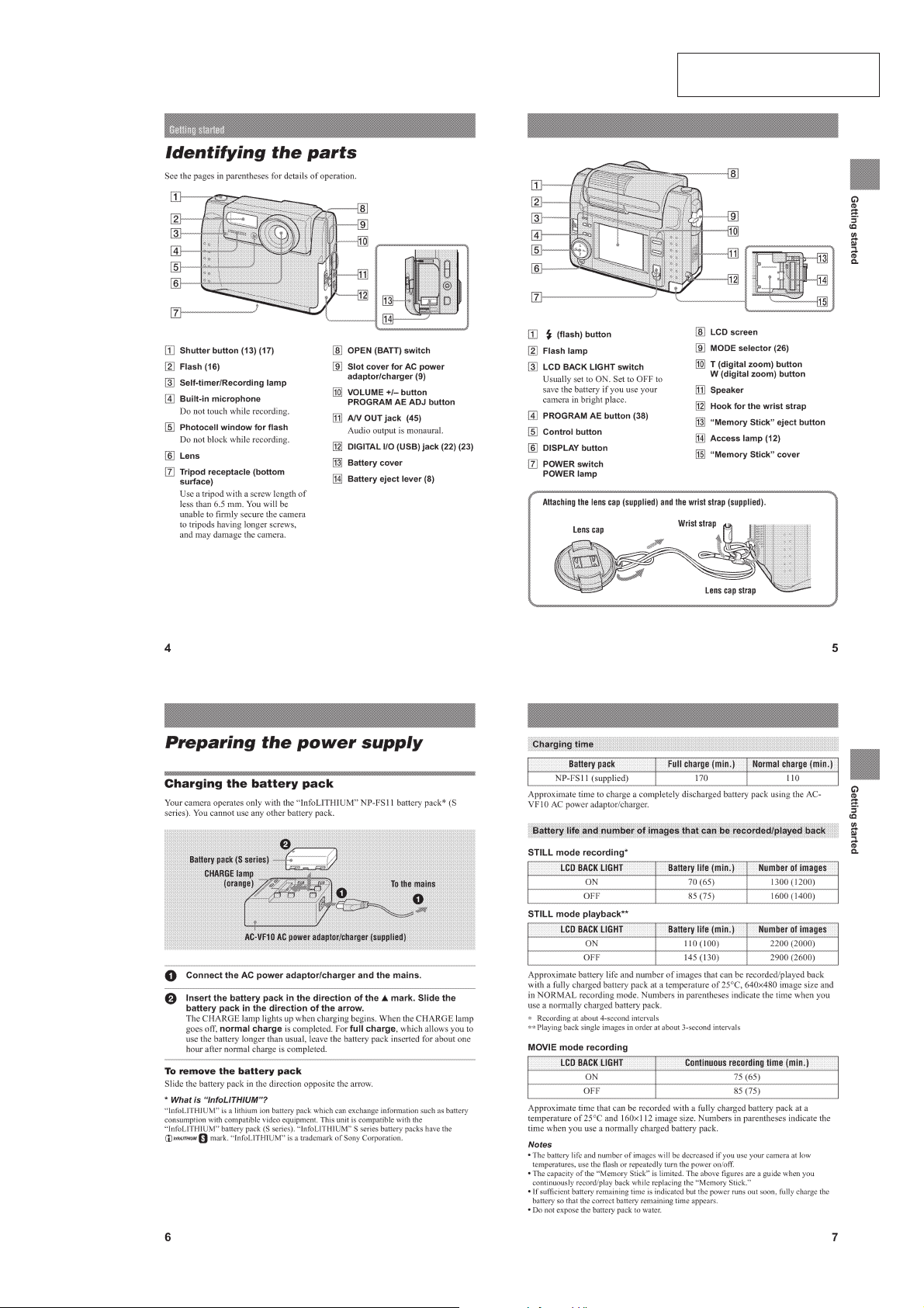
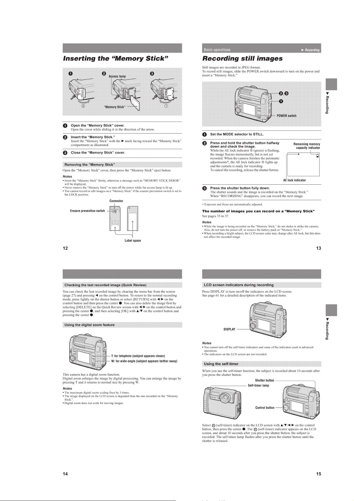
Identifying the parts ·······························································1-1
Preparing the power supply ··················································· 1-1
Setting the date and time························································1-2
Inserting the “Memory Stick”················································1-3
Basic operations
B Recording
Recording still images ···························································1-3
Recording moving images ·····················································1-4
B Playback
Playing back still images ······················································· 1-4
Playing back moving images ·················································1-4
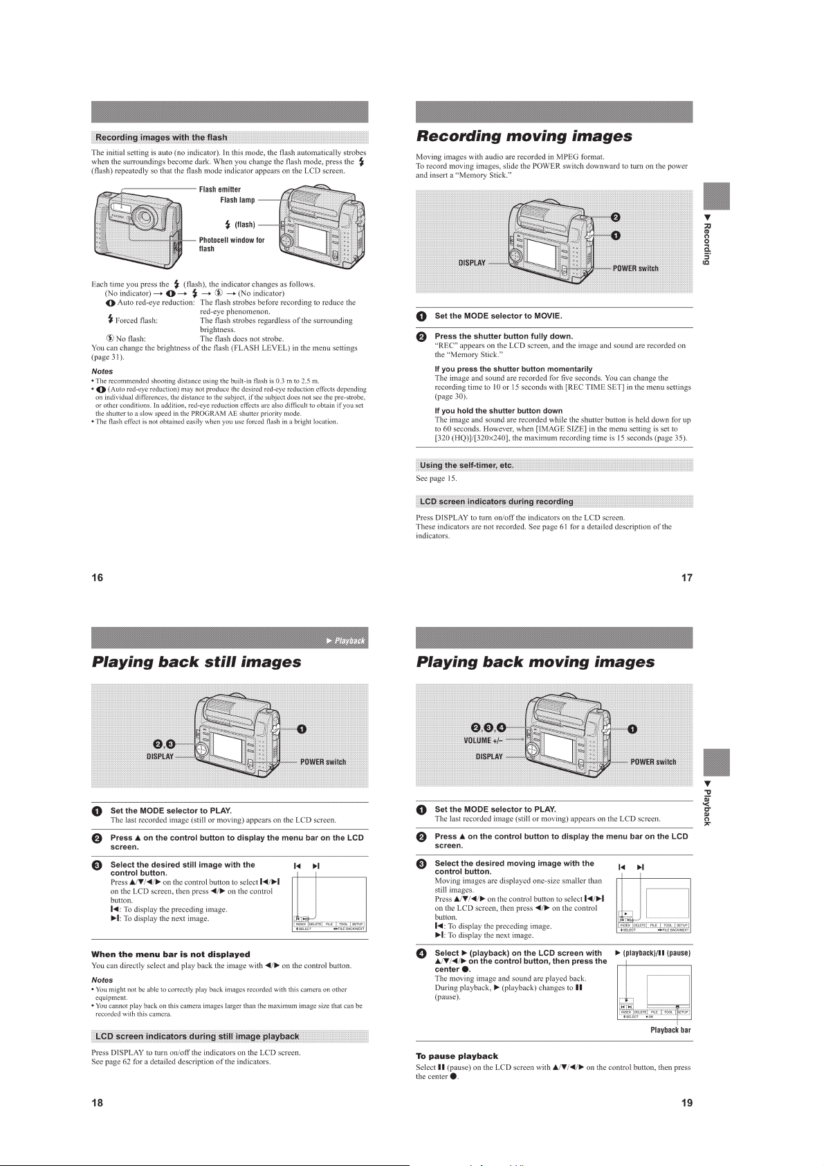
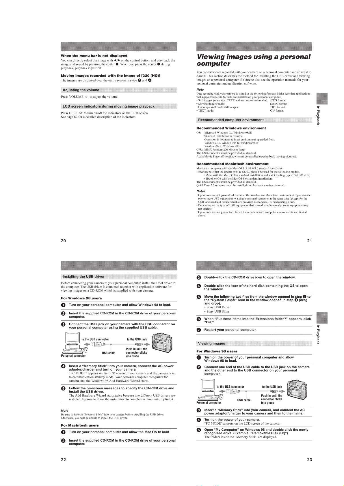
Viewing images using a personal computer ··························1-5
Image file storage destinations and image files ·····················1-6
Advanced operations
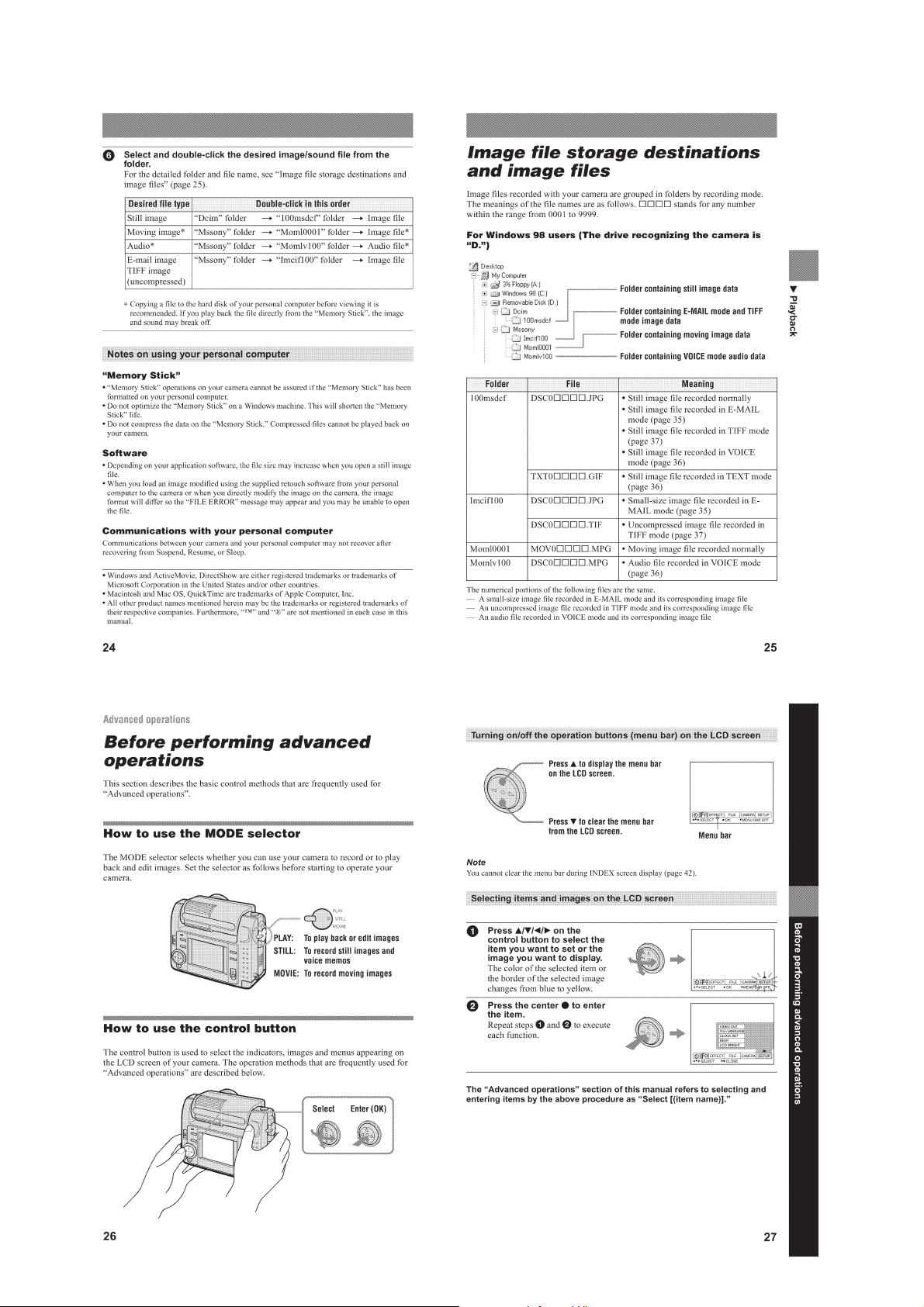
Before performing advanced operations
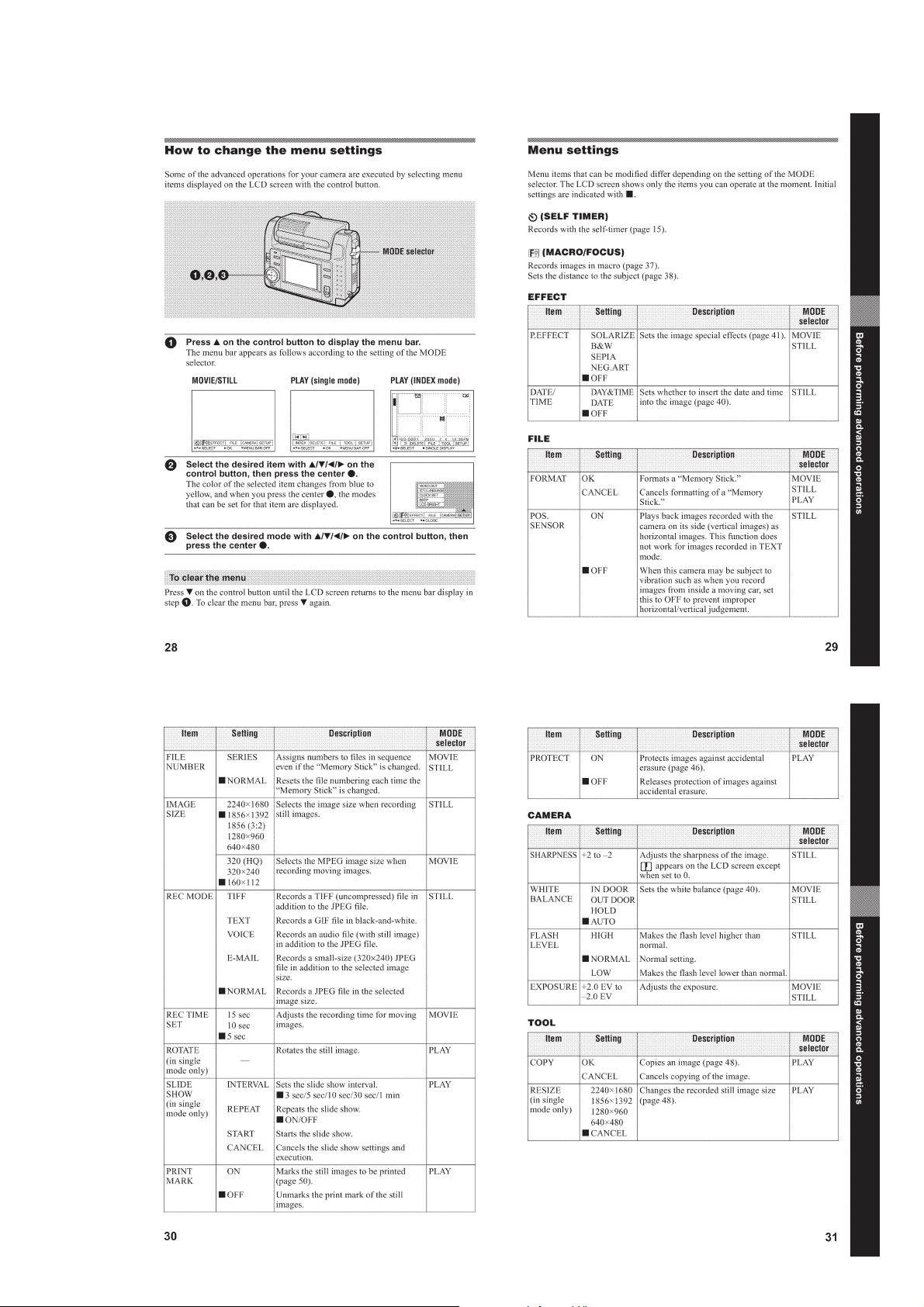
How to use the MODE selector ·············································1-6
How to use the control button················································1-6
How to change the menu settings ··········································1-7
Menu settings·········································································1-7
B V arious recording
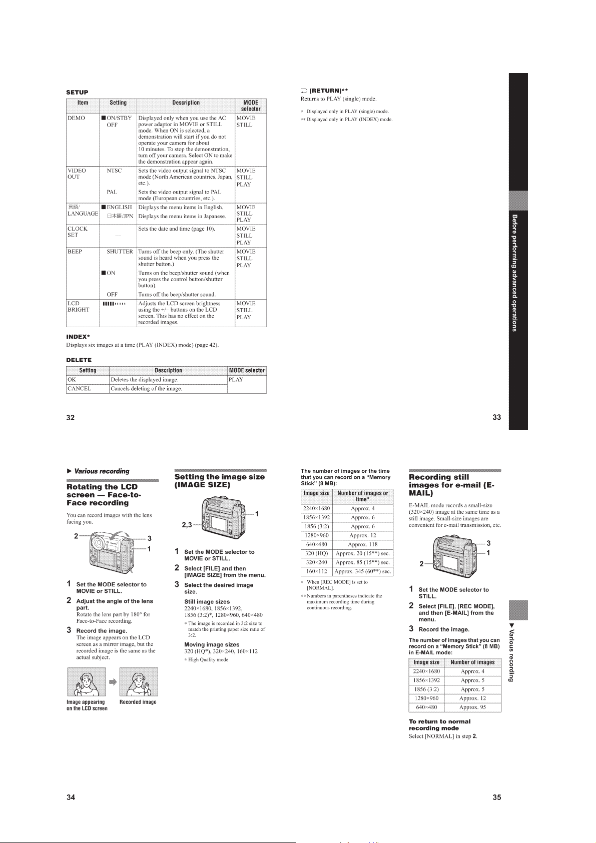
Rotating the LCD screen — Face-to-Face recording ············ 1-8
Setting the image size (IMAGE SIZE) ··································1-8
Recording still images for e-mail (E-MAIL)·························1-8
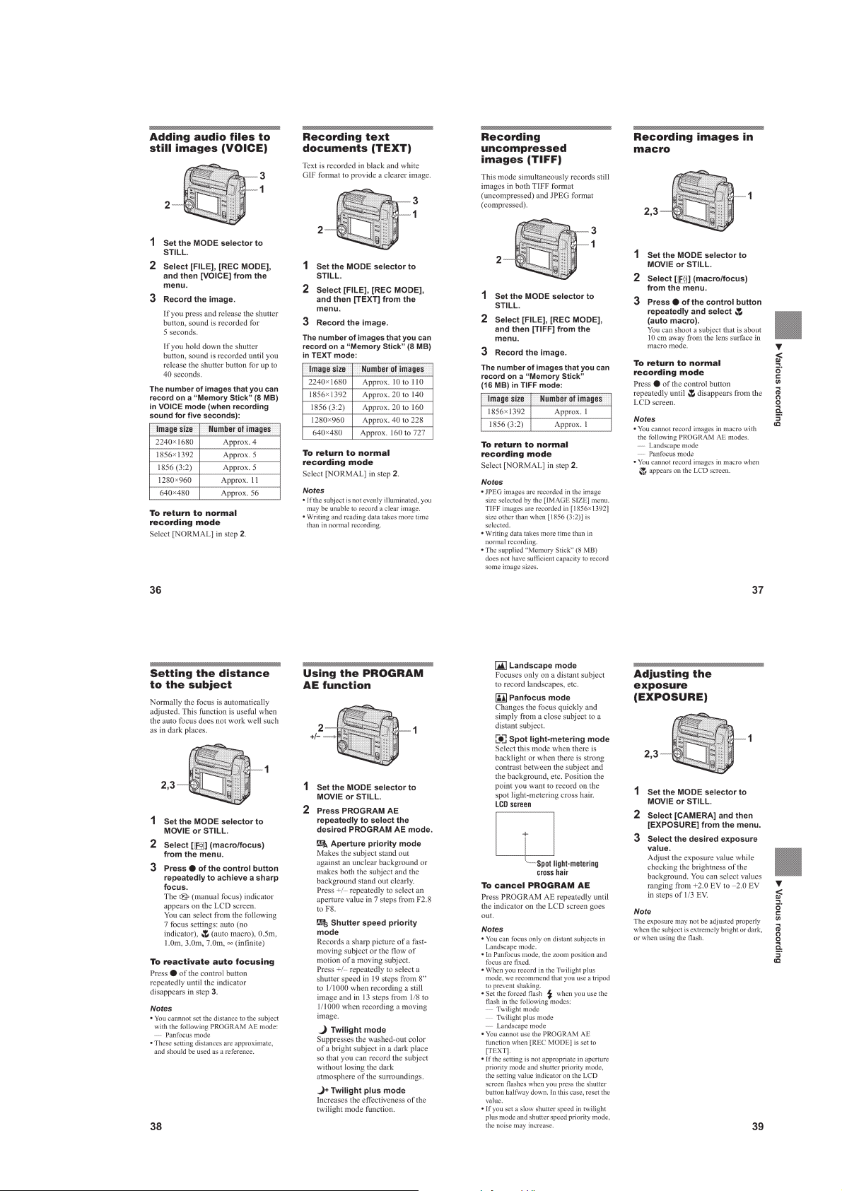
Adding audio files to still images (VOICE) ··························1-9
Recording text documents (TEXT) ·······································1-9
Recording uncompressed images (TIFF)·······························1-9
Recording images in macro ··················································· 1-9
Setting the distance to the subject··········································1-9
Using the PROGRAM AE function ·······································1-9
Adjusting the exposure (EXPOSURE) ··································1-9
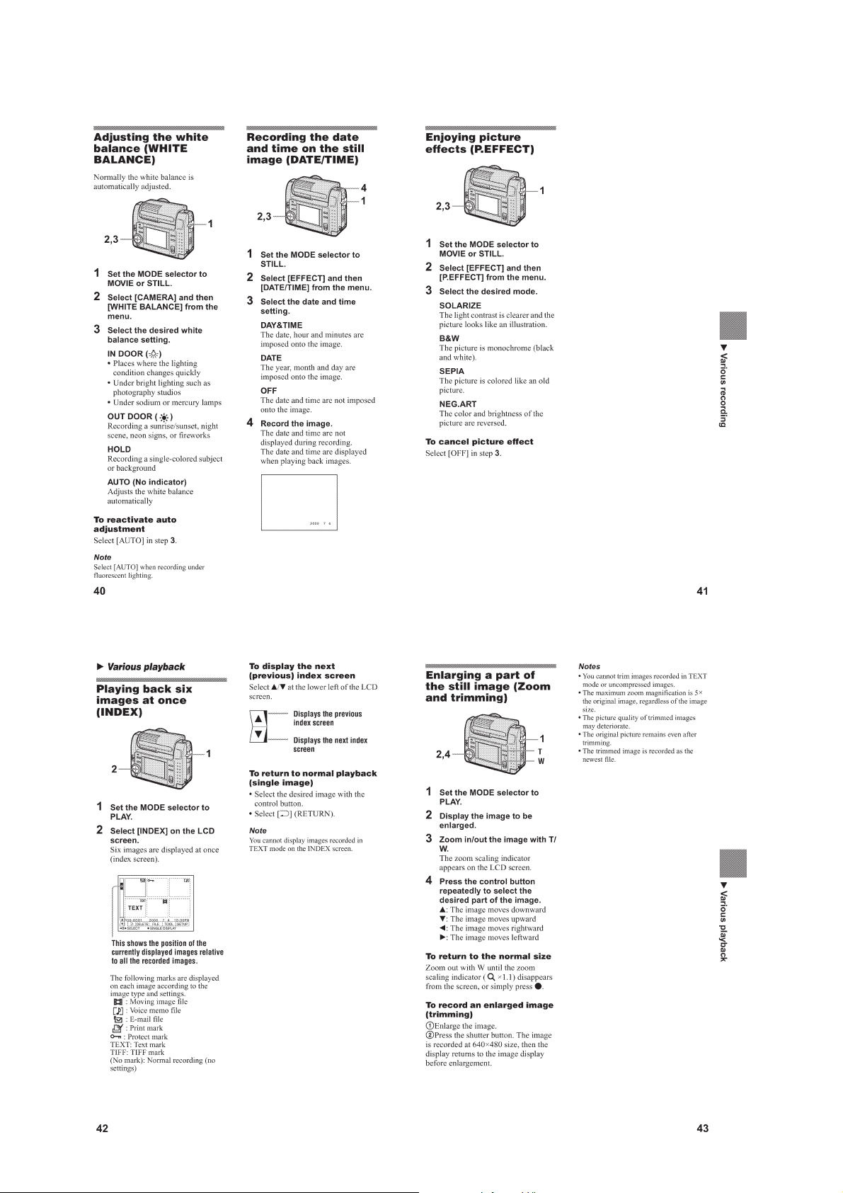
Adjusting the white balance (WHITE BALANCE) ············1-10
Recording the date and time on the still image
(DATE/TIME)······································································ 1-10
Enjoying picture effects (P.EFFECT) ·································· 1-10
B V arious playback
Playing back six images at once (INDEX) ··························1-10
Enlarging a part of the still image (Zoom and trimming)····1-10
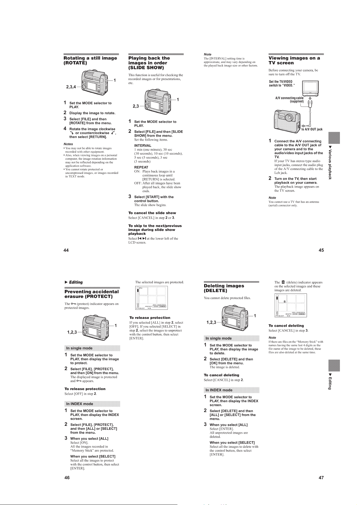
Rotating a still image (ROTATE) ·········································1-11
Playing back the images in order (SLIDE SHOW) ·············1-11
Viewing images on a TV screen ·········································· 1-11
B Editing
Preventing accidental erasure (PROTECT) ·························1-11
Deleting images (DELETE) ················································1-11
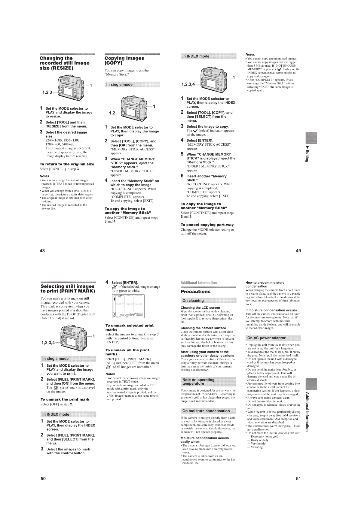
Changing the recorded still image size (RESIZE)···············1-12
Copying images (COPY) ·····················································1-12
Selecting still images to print (PRINT MARK) ·················· 1-12
Additional information
Precautions···········································································1-12
On “Memory Sticks” ···························································1-13
Using your camera abroad ···················································1-13
Troubleshooting ···································································1-13
Warning and notice messages ··············································1-14
Self-diagnosis display ··························································1-14
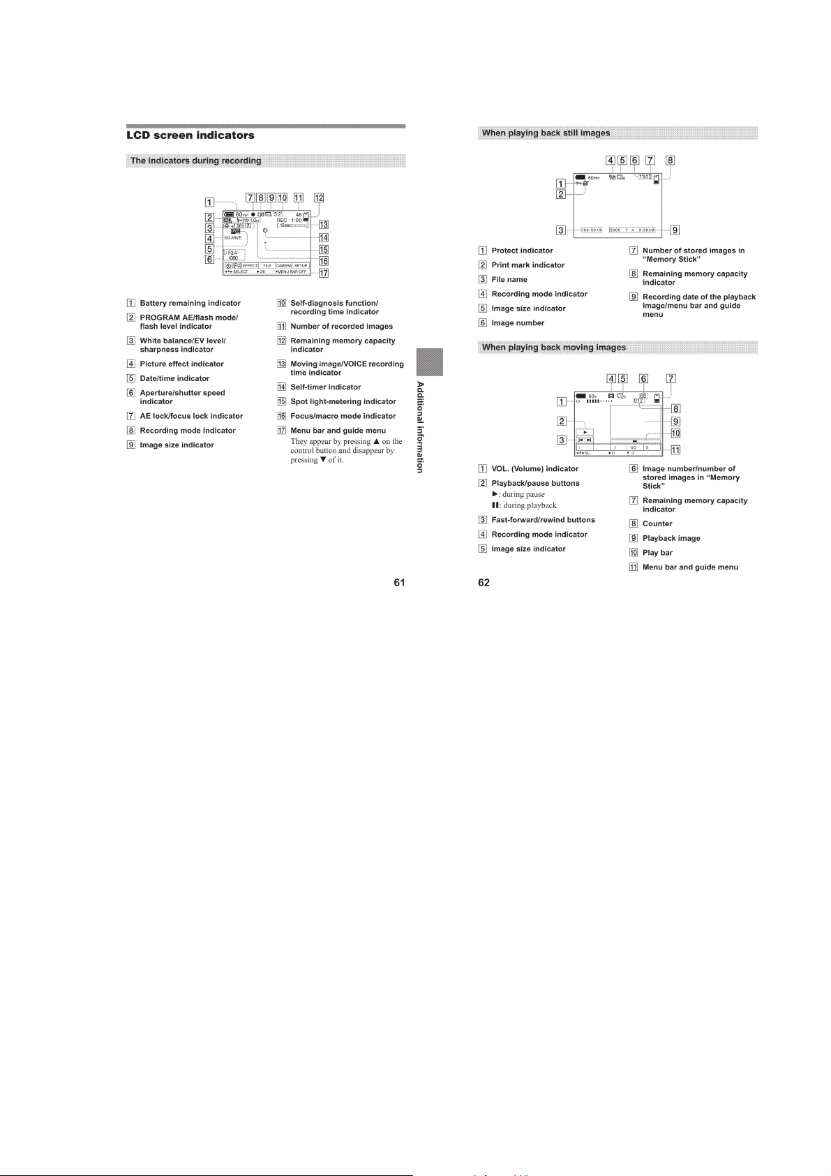
LCD screen indicators ·························································1-15
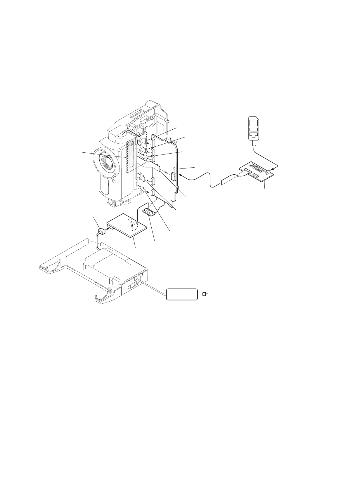
2. DISASSEMBLY
2-1. CABINET (FRONT) ASSEMBLY, CHECK COVER ····2-1
2-2. DD-143 BOARD ·····························································2-2
2-3. CAMERA BLOCK ASSEMBLY····································2-2
2-4. SY-59 BOARD ································································2-3
2-5. LCD PANEL BLOCK, SPEAKER (2.0CM),
CONTROL SWITCH BLOCK (MS)/(HF) ·····················2-5
2-6. LCD, INVERTER TRANSFORMER UNIT ··················2-6
2-7. LENS ASSEMBLY, FLASH UNIT,
MICROPHONE UNIT ····················································2-6
2-8. CIRCUIT BOARDS LOCATION ···································2-7
2-9. FLEXIBLE BOARDS LOCATION ································2-7
3. BLOCK DIAGRAMS
3-1. OVERALL BLOCK DIAGRAM (1/2) ···························3-1
3-2. OVERALL BLOCK DIAGRAM (2/2) ···························3-3
3-3. POWER BLOCK DIAGRAM (1/2) ································3-5
3-4. POWER BLOCK DIAGRAM (2/2) ································3-7
Founctional block diagrams are not shown.
Pages from 3-9 to 3-16 are not shown.
4. PRINTED WIRING BOARDS AND
SCHEMATIC DIAGRAMS
4-1. FRAME SCHEMATIC DIAGRAM································4-1
4-2. PRINTED WIRING BOARDS AND SCHEMATIC
DIAGRAMS····································································4-4
• CD-264 (CCD IMAGER)
PRINTED WIRING BOARD ·························4-5
• CD-264 (CCD IMAGER)
SCHEMATIC DIAGRAM ······························4-7
Schematic diagram and printed wiring board of the SY59 board are not shown.
Pages from 4-9 to 4-36 are not shown.
• CONTROL SWITCH BLOCK (MS/HF)
SCHEMATIC DIAGRAM ····························4-37
• DD-143 (DC/DC CONVERTER)
SCHEMATIC DIAGRAM ····························4-39
• DD-143 (DC/DC CONVERTER)
PRINTED WIRING BOARD ·······················4-41
4-3. WA VEFORMS ······························································ 4-43
4-4. MOUNTED PARTS LOCATION ·································4-48
5. ADJUSTMENTS
1. Before starting adjustment···············································5-1
1-1. Adjusting items when replacing main parts and boards··5-2
5-1. ADJUSTMENTS·····························································5-3
1-1. PREPARATIONS BEFORE ADJUSTMENT ·················5-3
1-1-1.List of Service Tools ························································5-3
1-1-2.Preparations ·····································································5-4
1-1-3.Discharging of the strobe power supply ··························5-4
1-1-4.Precaution ········································································5-6
1. Setting the Switch····························································5-6
2. Order of Adjustments ······················································5-6
3. Subjects ···········································································5-6
1-2. INITIALIZATION OF B, D, E, F, 7 PAGE DATA ·········5-7
1-2-1.INITIALIZATION OF D PAGE DATA ··························5-7
1. Initializing the D Page Data ············································5-7
2. Modification of D Page Data···········································5-7
3. D Page Table ····································································5-7
1-2-2.Initializing the B, E, F, 7 Page Data ································5-8
1. Initializing the B, E, F, 7 Page Data ································ 5-8
2. Modification of B, E, F, 7 Page Data·······························5-8
3. F Page Table ···································································· 5-9
4. 7 Page Table···································································5-10
5. E Page Table ··································································5-11
6. B Page Table ··································································5-11
1-3. VIDEO SYSTEM ADJUSTMENTS·····························5-12
1. Video Output Level Adjustment (SY-59 board) ············5-12
1-4. CAMERA SYSTEM ADJUSTMENTS························5-13
1. HALL Adjustment ·························································5-13
2. Flange Back Adjustment (Using Minipattern Box)·······5-14
— 3 —
Page 4

3. Flange Back Adjustment
(Using Flange Back Adjustment Chart) ························5-15
4. Flange Back Check························································5-15
5. F No. Standard Data Input·············································5-15
6. Mechanical Shutter Adjustment ····································5-16
7. Picture Frame Setting ····················································5-17
8. Light Level Adjustment and ND Shutter Check············5-18
9. Mixed Color Cancel Adjustment ···································5-18
10. Auto White Balance Standard Data Input ·····················5-19
11. Auto White Balance Adjustment ···································5-19
12. Color Reproduction Adjustment····································5-20
13. Color Reproduction Check ············································5-21
14. White Balance Check ····················································5-22
15. Strobe White Balance Adjustment·································5-23
16. Strobe Light Level and White Balance Check ··············5-23
17. CCD Black Defect Compensation·································5-24
18. CCD White Defect Compensation ································ 5-24
1-5. LCD SYSTEM ADJUSTMENT ···································5-25
1. LCD Initial Data Input ··················································5-25
2. VCO Adjustment (SY-59 board) ···································5-26
3. D Range Adjustment (SY-59 board) ······························5-26
4. Bright Adjustment (SY-59 board)··································5-27
5. Contrast Adjustment (SY-59 board) ······························5-27
6. Color Adjustment (SY-59 board) ···································5-28
7. V-COM Level Adjustment (SY-59 board) ····················· 5-28
8. V-COM Adjustment (SY-59 board) ·······························5-29
9. White Balance Adjustment (SY-59 board) ····················5-29
1-6. SYSTEM CONTROL SYSTEM ADJUSTMENT ········5-30
1. Battery End Adjustment (SY-59 board)························· 5-30
5-2. SERVICE MODE ··························································5-31
2-1. ADJUSTMENT REMOTE COMMANDER ················5-31
1. Using the Adjustment Remote Commander··················5-31
2. Precautions Upon Using the Adjustment Remote
Commander ··································································· 5-31
2-2. DATA PROCESS··························································· 5-32
2-3. SERVICE MODE ··························································5-33
1. Setting the Test Mode ····················································5-33
2. Bit V alue Discrimination ··············································· 5-33
3. Emergency Memory Address of Flash Unit ··················5-33
4. Record of Use check······················································5-34
5. Self Diagnostics Log check ···········································5-34
6. Switch check (1) ····························································5-35
7. Switch check (2) ····························································5-35
8. LED check····································································· 5-35
9. Position sensor check (SY-59 board SE401) ·················5-36
6. REPAIR PARTS LIST
6-1. EXPLODED VIEWS ······················································6-1
6-1-1.OVERALL SECTION·····················································6-1
6-1-2.CABINET (FRONT) SECTION ·····································6-2
6-1-3.CAMERA BLOCK SECTION ·······································6-3
6-1-4.CABINET (REAR) SECTION ·······································6-4
6-2. ELECTRICAL PARTS LIST ··········································6-5
Electrical parts list of the SY-59 board is not shown.
pages 6-8 to 6-14 are not shown.
* Color reproduction frame is shown on page 105.
— 4 —
Page 5
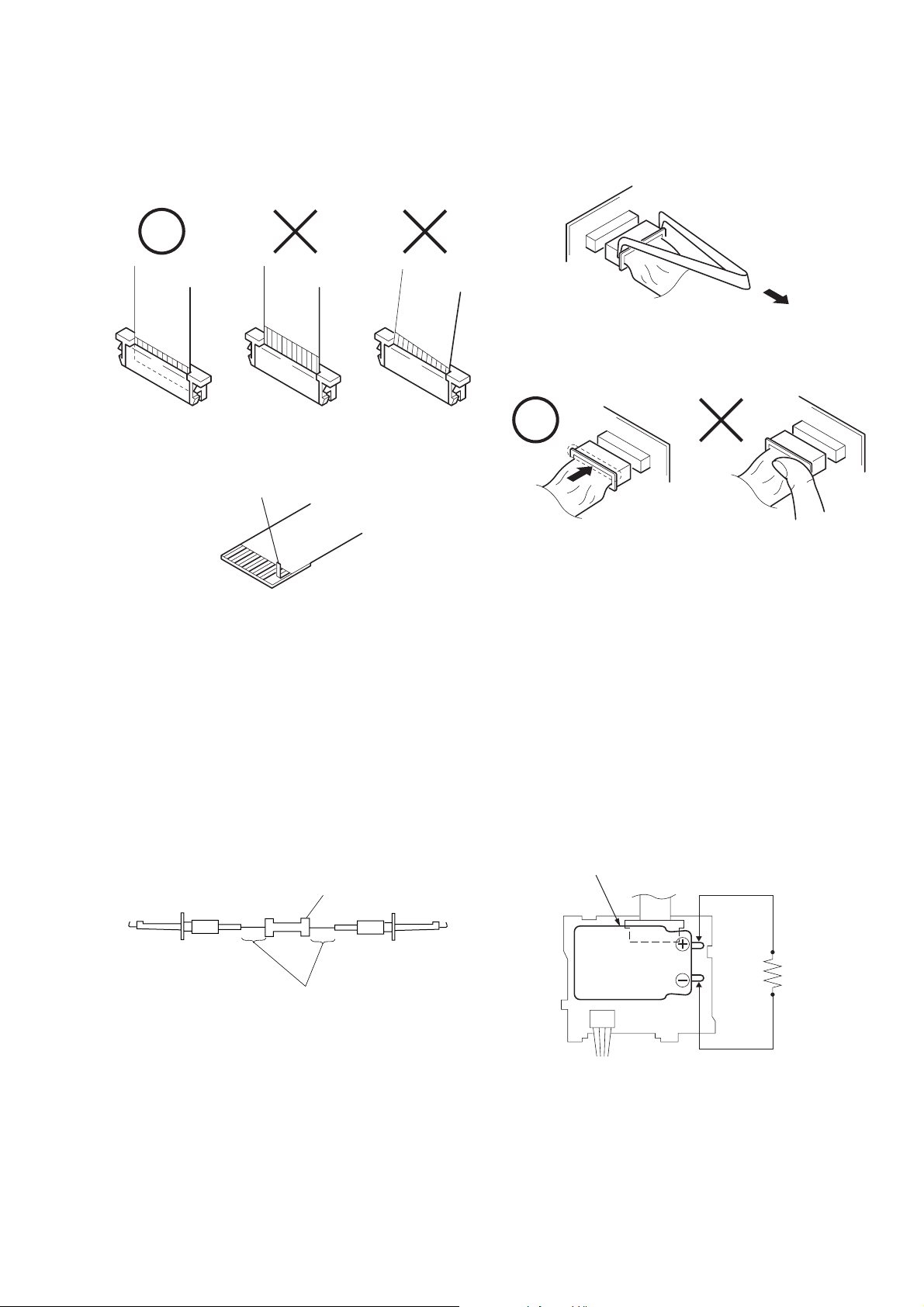
• NOTE FOR REPAIR
SERVICE NOTE
Make sure that the flat cable and flexible board are not cracked of
bent at the terminal.
Do not insert the cable insufficiently nor crookedly.
Cut and remove the part of gilt
which comes off at the point.
(Take care that there are
some pieces of gilt left inside)
When remove a connector, don't pull at wire of connector.
Be in danger of the snapping of a wire.
When installing a connector, don't press down at wire of connector.
Be in danger of the snapping of a wire.
[Discharging of the FLASH unit’s charging capacitor]
The charging capacitor of the FLASH unit is charged up to the
maximum 300 V potential.
There is a danger of electric shock by this high voltage when the
capacitor is handled by hand. The electric shock is caused by the
charged voltage which is kept without discharging when the main
power of the DSC-F55V is simply turned off. Therefore, the
remaining voltage must be discharged as described below.
Preparing the Short Jig
To preparing the short jig. a small clip is attached to each end of a
resistor of 1 kΩ /1 W (1-215-869-11)
Wrap insulating tape fully around the leads of the resistor to prevent
electrical shock.
1 kΩ/1 W
Wrap insulating tape.
Discharging the Capacitor
Short circuits between the positive and the negative terminals of
charged capacitor with the short jig about 10 seconds.
Capacitor
Short jig
FLASH UNIT
— 5 —
Page 6

[Description on Self-diagnosis Display]
Self-diagnosis display
• C: ss: ss
The contents which can be handled
by customer, are displayed.
• E: ss: ss
The contents which can be handled
by engineer, are displayed.
Display Code
C:32:01
C:13:01
E:91:01
Turn off the main power then back on.
Replace the memory stick.
Format the memory stick with the DSCF55V.
Checking of flash unit or replacement of
flash unit
Countermeasure
Trouble with hardware.
• The type of memory stick that cannot
be used by this machine, is inserted.
• Data is damaged.
• Unformatted memory stick is inserted.
Abnormality when flash is being
charged. *2
E:61:00 *1
Checking of lens drive circuit
When failed in the focus initialization.
E61:10 *1
Note : The error code is cleared if the battery is removed, except defective flash unit.
*1: The error display is given in two ways.
*2: When the flash charginf failed, Page: D, Address: 67, Data:04 are written.
After repair, be sure to write Page: D, Address: 67, Data: 00.
Cause
Caution Display During Error
SYSTEM ERROR
MS ERROR
Flash LED
Flash display
Flashing at 3.2 Hz
—
— 6 —
Page 7
SECTION 1
GENERAL
DSC-F55V
This section is extracted from
instruction manual.
1-1
Page 8
1-2
Page 9
1-3
Page 10
1-4
Page 11
1-5
Page 12
1-6
Page 13
1-7
Page 14
1-8
Page 15
1-9
Page 16
1-10
Page 17
1-11
Page 18
1-12
Page 19
1-13
Page 20
1-14
Page 21
1-15E
Page 22
SECTION 2
DISASSEMBLY
The following flow chart shows the disassembly procedure.
2-1. Cabinet (front) assembly,
Check cover
2-2. DD-143 board
DSC-F55V
2-3. Camera block assembly
2-4. SY-59 board
DSC-F55V
Main (SY-59) board, DD-143 board
LCD service position
NOTE: Follow the disassembly procedure in the numerical order given.
2-1. CABINET (FRONT) ASSEMBLY, CHECK COVER
P
DD-143,CD-264 boards
service position
2-7. Lens assembly, Flash unit,
Microphone unit
2-5. LCD panel block, Speaker (2.0cm),
Control switch block (MS) / (HF)
2-6. LCD, Inverter transformer unit
(Fig 1)
Remove the check cover by rotating
the metal bar in the direction of the
arrow of ø1.6 or less centering around
the point “P”.
Note: Do not reuse the check cover
that is once removed.
3
Two screws (M1.7 × 3),
lock ace, p2
4
Battery terminal
board (3p)
1
Screw (M1.7 × 3), lock ace, p2
5
Cabinet (front) assembly
2
Two screws (M1.7 × 3),
lock ace, p2
SY-59
6
Check cover
(Refer to Fig 1)
2-1
Page 23
2-2. DD-143 BOARD
)
qs
DD-143 board
9
DD shield case B
4
qa
DD shield case A
8
q;
Two claws
Claw
DD-143
Screw (M1.7 × 3), lock ace, p2
2
Harness (MC-081) (3p)
3
Harness (DB-51) (5p)
1
FP-109 flexible board
(40p)
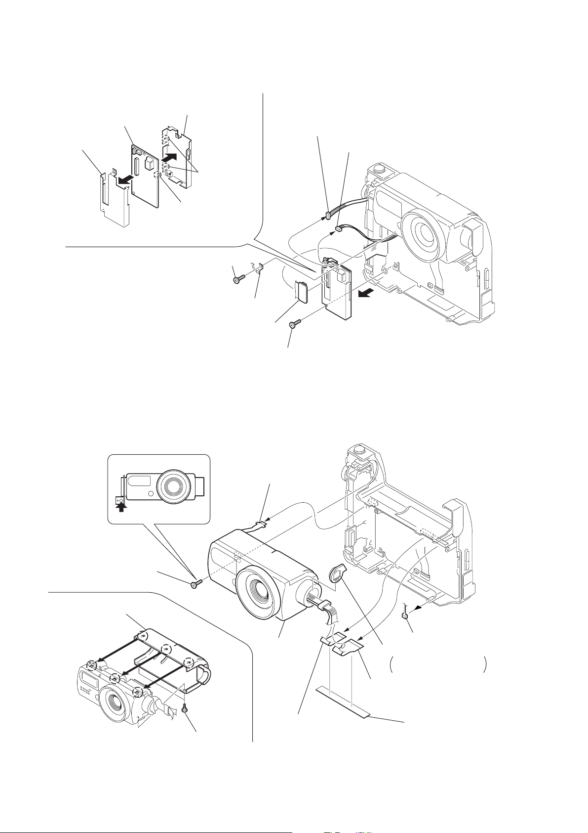
2-3. CAMERA BLOCK ASSEMBLY
6
Screw (M2 × 4.5),
tapping head (2 lock)
5
Plate nut
4
FP-108 flexible board (9p)
7
6
Screw (M1.7 × 3), lock ace, p2
SY-59
q;
Lens cabinet (rear) assembly
(Remove the three claws.)
9
Two step screws
7
Camera
block assembly
3
Flexible board
(from lens block) (16p)
2-2
5
Harness (DC-67) (3p
8
Flexible stabilizer
Be careful when handling
it as it is not fixed.
2
FP-107 flexible board (22p)
1
Flexible retainer sheet
Page 24
[ DD-143, CD-264 BOARDS SERVICE POSITION ]
Note 1: The built-in charging capacitor inside the FLASH unit is charged to the maximum of 300 V.
There is a danger of electric shock due to the high voltage when the battery is handed by
bare hand. Discharge the voltage remained in the battery, referring to the Service Note (See page 5).
FP-108 flexible board (9p)
Harness (MC-081) (3p)
Harness (DC-67) (3p)
Battery terminal board (3p)
Harness (DB-51) (5p)
AC POWER
ADAPTOR
2-4. SY-59 BOARD
AC IN
DD-143
Flexible board
CD-264
(from lens assembly) (16p)
FP-107 flexible board (22p)
Adjustment remote
commander (RM-95)
SY-59
CPC-9 jig
FP-109 flexible board (40p)
(J-6082-393-C) (Note 2)
Note 2: The old CPC-9 jig (Parts code: J-6082-393-B)
cannot be used, because it cannot operate
the adjustment remote commander.
Note 3: Don't use the 12pin flexible board of CPC-9 jig.
It causes damage to the unit.
qg
Screw (M1.7 × 3),
lock ace, p2
qh
DD flame
3
Flexible board
(from control switch block (MS))
(15p)
9
Screw (M1.7 × 3), lock ace, p2
4
Flexible board
(from control switch block (HF))
(6p)
5
Harness (DC-67) (3p)
7
Flexible board
SY-59
board
2
FP-108 flexible board (9p)
qd
(from lens assembly) (16p)
FP-109 flexible board (40p)
SY-59
board
qa
Claw
8
FP-101 flexible board (22p)
qs
1
FP-110 flexible board (24p)
qf
SY-59 board
q;
Two screws (M1.7 × 3), lock ace, p2
6
Flexible retainer sheet
2-3
Page 25
[ MAIN (SY-59) BOARD, DD-143 BOARD, LCD, SERVICE POSITION ]
Note 1: The old CPC-9 jig (Parts code: J-6082-393-B) cannot be used,
because it cannot operate the adjustment remote commander.
Note 2: Don't use the 12pin flexible board of CPC-9 jig.
It causes damage to the unit.
FP-101 flexible board (22p)
Flexible board
(from lens assembly) (16p)
LCD
SY-59
board
Flexible board
(from control switch block (HF))
(6p)
SY-59 board
FP-110 flexible board (24p)
Adjustment remote
commander (RM-95)
CPC-9 jig
(J-6082-393-C) (Note 2)
Battery terminal board (3p)
DD-143
board
FP-109 flexible board (40p)
DD-143 board
Flexible board
(from control switch block (MS))
(15p)
FP-108 flexible board (9p)
AC POWER
ADAPTOR
AC IN
2-4
Page 26
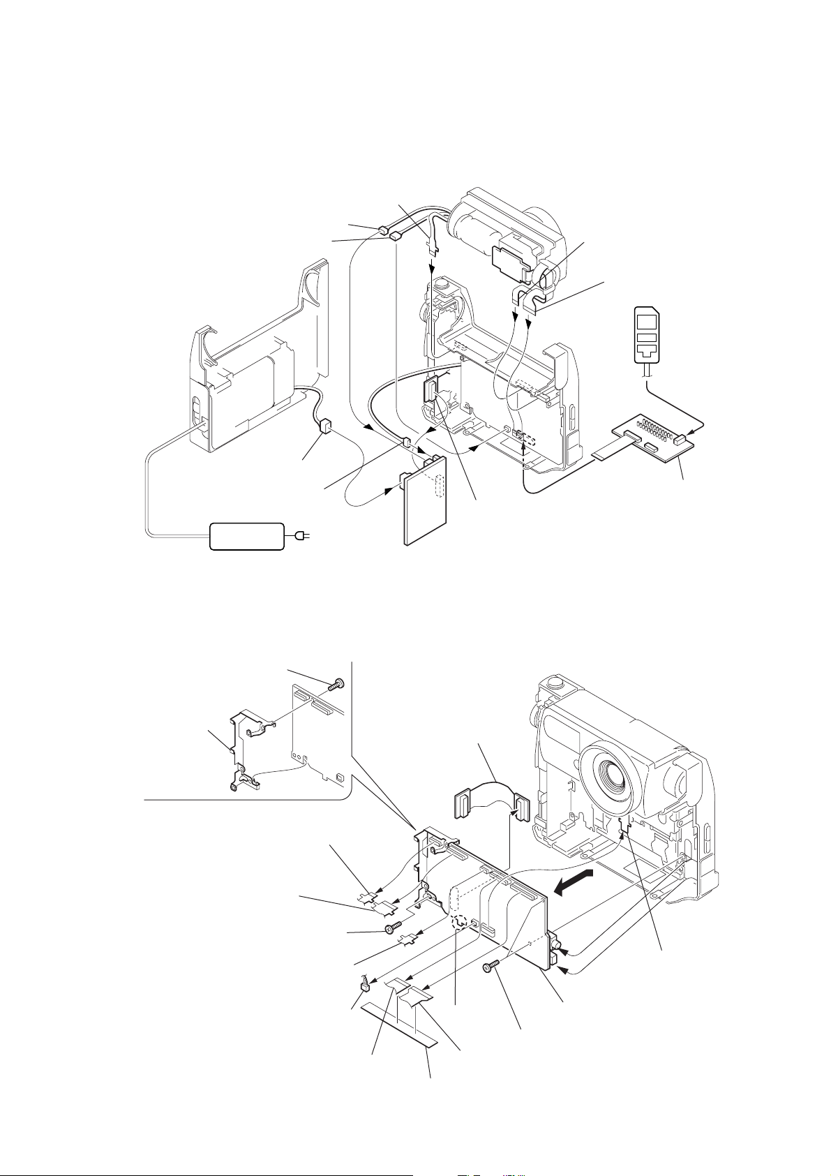
2-5. LCD PANEL BLOCK, SPEAKER (2.0CM), CONTROL SWITCH BLOCK (MS)/(HF)
0
LCD panel block
8
Function knob
6
HF cushion
2
Screw (M2 × 4.5),
tapping head (2 lock)
1
Panel insulating sheet
3
Two screws (M2 × 4.5),
tapping head (2 lock)
7
Three screws (M2 × 4.5),
tapping head (2 lock)
4
Control switch block (MS)
Control switch block (MS)
Control switch block (HF)
9
Control switch block (HF)
5
Speaker (2.0 cm)
2
Mode dial
4
AE leaf spring
assembly
1
T apping screw
3
Sleeve
Rear cabinet
REMOVING THE SLEEVE AND
THE AE LEAF SPRING ASSEMBLY
PRECAUTION DURING
INSTALLATION
Note : When installing it,
align the sleeve and
the mode dial as shown.
When installing it,
align the switch position
as shown.
PRECAUTION DURING
INSTALLATION
When installing it,
align the switch position
as shown.
2-5
Page 27

2-6. LCD, INVERTER TRANSFORMER UNIT
n
e
qs
Cold cathode fluorescent tube
7
Harness (DB-51) (5p)
8
Inverter transformer unit
3
Screw (M1.7 × 2),
lock ace, p2
9
Screw (M1.7 × 2),
lock ace, p2
q;
FP-110 flexible board
5
4
Two claws
qa
Back light sheet
6
Cold cathode fluorescent tube (20p)
2
Crystal indication modul
1
Crystal indication module (23p)
2-7. LENS ASSEMBLY, FLASH UNIT, MICROPHONE UNIT
Note : The built-in charging capacitor inside the FLASH unit is charged to the maximum of 300 V.
There is a danger of electric shock due to the high voltage when the capacitor is handed by
bare hand. Discharge the voltage remained in the capacitor, referring to the Service Note
q;
Two screws (M2 × 4.5), tapping head (2 lock)
qs
qd
Sound absorption sheet (D)
qa
Microphone cushion
Microphone retainer
6
Harness (MC-081) (3p)
Be careful when handling
it as it is not fixed.
qf
Microphone unit
9
Harness (DC-67) (3p)
7
Lens block assembly
7
CCD block assembly
(CCD imager)
6
Seal rubber (K)
5
Optical filter block
4
CCD fitting adaptor (K)
2
Lens assembly
(See page 5).
CD
8
CD-264 board
1
T wo tapping
screws (B1.7
3
Two claws
8
Flash unit
Remove the three
claws as shown.
5
Microphone unit (2p)
4
-264
×
6)
Two screws (M2 × 4.5),
tapping head (2 lock)
3
FP-107 flexible
board
2
Flexible cushio
1
Lens flexible ring
REMOVING THE CD-264 BOARD, LENS ASSEMBLY
2-6
Page 28

2-8. CIRCUIT BOARDS LOCATION
FLASH UNIT
DD-143
(DC-DC CONVERTER)
CD-264
(CCD IMAGER)
INVERTER TRANSFORMER UNIT
SY-59
CAMERA, CAMERA DSP,
LCD DRIVE, TIMING GENERATOR,
VIDEO, SH DSP, AUDIO,
LENS MOTOR DRIVE, HI CONTROL,
A/V OUT, USB, CONNECTOR
2-9. FLEXIBLE BOARDS LOCATION
FP-108
CONTROL SWITCH
BLOCK (MS)
FP-109
FP-110
FLEXIBLE BOARD
(From CAM MOTOR)
CONTROL SWITCH
BLOCK (HF)
FP-107
2-7E
Page 29

SECTION 3
BLOCK DIAGRAMS
DSC-F55V
3-1. OVERALL BLOCK DIAGRAM (1/2)
IRIS
METER
HALL
H
XFC RST SENS
FLASH
UNIT
IRIS
(SHUTTRE)
HALL (+)
MM
FLASH
UNIT
LENS
FOCUS
MOTOR
FOCUS
MOTOR
DRIVE
IC201
ENO
DIROA
DIROB
FOCUS
RESET
SENSOR
SHUTTER
DRIVE
(4-27)
MSHUT ON
BT901
BATTERY
TERMINAL
( ) : Page No. shown in ( ) indicates the page to refer on the schematic diagram.
CD-264 BOARD(1/2)
(4-8)
IC102
CCD IMAGER
IC202
IRIS CONT 1,2
IC203
IRIS DRIVE
HALL AMP
(4-27)
HALL AD
STRB ON
ST UNREG
STB CHARGE
V1,V1B,V2,
V3A,V3B,V4,
RG,VSHT
H1,H2
CCD OUT
SY-59 BOARD
(4-9)
IC102
S/H,AGC,
A/D CONV.
(4-9)
IC101
TIMING
GENERATOR
CAM SO,XCAM,SCK
(4-12)
IC204
EVR
MCK18
AD DATA
(4-14)
IC303
IC304
SDRAM
64MbitX2
MCK18
ADDRESS
14
16
XFC RST SENS
MSHUT ON
ENO
DIROA
DIROB
STRB ON
DATA
1212
(4-11)
IC301
CAMERA DSP
MEMORY CONTROL
VIDEO ENCODER
OPD,OSD,HOST IF
RES CONTROL
SG,JPEG,L-MODE
AUDIO I/F
SHUTTER CONTROL
STROBO CONTROL
CAM SO,XCAM SCK
16
14
MC XCS2
MC XCS6
AU SDTO
AU SDTI
Y
C
Y
R-Y
B-Y
VD,HD
(4-19)
IC651
VIDEO AMP
DATA BUS
ADDRESS BUS
VIDEO OUT
CONTENUDE ON
(SEE PAGE
3-3)
S
IC001
IC002
DC/DC
CONVERTER
(4-39,40)
ST UNREG
DD-143 BOARD
16
BATT SIG
CAM DD ON
SYS DD ON
LCD DD ON
M 5V
A 4.9V
CAM -7.5V
CAM 15V
D 3.2V
A 3.2V
D 1.8V
PANEL -15V
PANEL 13.5V
PANEL 6.5V
PANEL 4.9V
EVER 3.5V
HI UNREG
3-1 3-2
Page 30

DSC-F55V
3-2. OVERALL BLOCK DIAGRAM (2/2)
SY-59 BOARD
DATA BUS
16
ADDRESS BUS
20
(4-21)
IC501
MC CAM
SH DSP
MC XCS2
MC XCS6
CONTENUDE ON
(SEE PAGE
3-2)
(4-24)
IC507
EEPROM
CAM SO,XCAM SCK
AU SDTO
AU SDTI
HALL AD
(4-25)
IC252
AUDIO
AD/DA
CONV.
AU OUT
AU IN
MIC SIG
( ) : Page No. shown in ( ) indicates the page to refer on the schematic diagram.
14
IC506
SDRAM
64Mbit
MC XCS2
USB D+/- OUT, USB D+/- IN
MS DIO, MS SCLK
EVER 3.5V
HI UNREG
HI SO,HI SI,XHI SCK
(4-25)
IC702
LINE/
SPEAKER
AMP
MIC AMP
16
(4-24) (4-24)
MC XCS0
(4-29)
AUDIO OUT
AU SP+,SP-
19
IC504
FLASH ROM
16Mbit
(4-29)
IC407
3.2V REG
IC408
RESET
16
(4-29)
EVER 3.2V
IC402
IC404
HI CONTROL
RESET
RESET
KEY AD 0
XCAM/PB SW
MOVIE/XSTILL SW
XPWR SW
(4-29)
XPOWER LED
XSHTR SW
XSHTR LOCK SW
(4-30)
IC406
EEPROM
BEEP
BATT SIG
STB CHARGE
SYS DD ON
LCD DD ON
CAM DD ON
KEY AD1
KEY AD2
STB LED
32KHZ
(4-32)
IC601
USB
I/F
IC405
(4-30)
TIMER
CLOCK
EVER 3.2V
USB D+
USB D-
BATT
CN951
USB
S104-106
DIGITAL ZOOM T/W SW
LENS SW
S102
PLAY/STILL/MOVIE SW
S101
POWER SW
D101
POWER LED
S103,107
SHUTTER SW
S101-107
FUNCTION SW
D103
FLASH LED
BT001
LITHIUM BATTERY
CONTROL
SWITCH
BLOCK(MS)
CONTROL
SWITCH
BLOCK(HF)
CN101
MEMORY
STICK
VIDEO OUT
(4-15)
HI SO,XHI SCK
IC801
EVR
(4-8)
MIC901
MIC
IC101
MIC
AMP
CD-264
BOARD(2/2)
16
3-3 3-4
VD,HD
Y
R-Y
B-Y
BL UNREG
VIDEO OUT
AUDIO OUT
AU SP+,SP-
(4-17)
IC901
TIMING
GENERATOR
IC803
(4-16)
LCD
DRIVE
INVERTER
UNIT
J951
A/V OUT
SP901
SPEAKER
LCD901
LCD
PANEL
R
G
B
ND901
BACK
LIGHT
UNIT
Page 31

DSC-F55V
3-3. POWER BLOCK DIAGRAM (1/2)
DD-143 BOARD
BT901
BATTERY
TERMINAL
S
BATT UNREG
BATT SIG
BATT GND
1
2
3
CN001
F001
F002
F003
F004
T003
DC/DC CONVERTER
5
7
8
4
1
Q011
SWITCHING
2
3
( ) : Page No. shown in ( ) indicates the page to refer on the schematic diagram.
D006
RECT
D001
RECT
V+=UN+2.2V
V-=UN-1.6V
VCC
=UN+2.2V
VG=8V
LCD 0N
CAM ON
DD ON
53
58
64
54
59
26
51
8
7
1
24
33
34
29
28
27
DC/DC CONVERTER
VCC(0)1-2
VCC(0)3,4
VCC(0)5,6,7
VSS(0)1-2
VSS(0)4,5,6
VCC
VG(0)1
+IN(E)7
-IN(E)7-2
OUT7
VREF
RT
CT
CTL6
CTL5
CTL1-4,7
IC001
-IN(A)6
-IN(E)6
-IN(C)5
-IN(E)5
-IN(C)8
-IN(E)4
-IN(E)3
OUT6
OUT5
OUT4
OUT3
(4-39)
T001
Q009
SWITCHING
1
63
Q010
SWITCHING
Q003,005,006
Q004,007,008
DRIVE
DRIVE
Q012
SWITCHING
L004
L005
4
4
3
2
1
Q021
SWITCHING
Q022
SWITCHING
Q019
SWITCHING
10
12
14-IN(C)6
62
17
18
23
61
21
60
36
Q014
D004(1/2)
RECT
8
7
2
3
5
5
6
7
8
T002
Q025
EMERGENCY
DETECT
L003
L001
D005
RECT
D007
RECT
4
D002
DC/DC CONV.
(STEP UP)
Q023(1/2)
Q024(1/2)
2
3
L016
L013
D004(2/2)
EMERGENCY
DETECT
L012
L009
Q023(2/2)
Q024(2/2)
IC002
Q030,031
Q016,017
Q032,033
L010
L015
L011
L005
L007
(4-40)
ST UNREG
BATT SIG
EVER +3.5
HI UNREG
PANEL +13.5V
PANEL +6.5V
PANEL -15V
PANEL +4.9V
CAM +15V
CAM -7.5V
A +4.9V
M +5V
D +1.8V
CN002
3
6
10
12
8
11
13
15
25
16
14
17
A4.9V
18
19
M5V
20
23
D1.8V
24
POWER(2/2)
(FLASH UNIT)
POWER(2/2)
(SY-59)
(ON PAGE
3-7)
BACK
LIGHT
UNIT
55
OUT2-1
L014
Q002(2/2)
Q029(2/2)
L008
Q002(1/2)
Q029(1/2)
57
OUT2-2
39
-IN(E)2
Q020
Q015
SWITCHING
SWITCHING
CAM ON
LCD ON
Q013
SWITCHING
48
OUT1-2
52
OUT1-1
49
CN003
BL UNREG
1
1
BL ON
3
3
BL PWM
4
4
BL LED ON
5
5
OUT1-3
-IN(E)1
44
L002
16
D +3.2V
A +3.2V
BL LED ON
BL ON
DD ON
LCD ON
CAM ON
BL PWM
CN004
26
27
28
29
30
32
9
4
1
2
3
5
D3.2V
A3.2V
XBL LED ON
SYS DD ON
LCD DD ON
CAM DD ON
BL PWM
3-5 3-6
Page 32

DSC-F55V
3-4. POWER BLOCK DIAGRAM (2/2)
SY-59 BOARD
BATT SIG
5
IC407
POWER(1/2)
(DD-143)
(ON PAGE
3-6)
9,11
10
26
16
14
12
15
13
23,24
25,27,28
29,30,31
17,18
19,20
EVER 3.5V
HI UNREG
7
XBL LED ON
6
4
3
2
1
CN705
BL PWM
CAM DD ON
BL ON
SYS DD ON
LCD DD ON
PANEL +4.9V
PANEL -15V
PANEL +6.5V
PANEL +13.5V
CAM 15V
CAM -7.5V
D 1.8V
D 3.2V
A 3.2V
A 4.9V
M5V
UNREG
10 18 17
VDD
CPC
3.2V
2
REG
IC408
RESET
RESET
CN704
FOR CHECK
3
12
L255
( ) : Page No. shown in ( ) indicates the page to refer on the schematic diagram.
(4-29)
(4-29)
Q253
IC402
2
EVER 3.2V
SP VCC
Q409
IF BLOCK
(4-29)
RESET
48
BATT SI
49
BATT SO
42,51
75,76
77,86
87
1
38
XREST
71
BATT SENS
72
ACV SENS
92
DD CON SENS
11
BL LED ON
43
BL ON
57
XBL PWM
25
CAM DD ON
47
LCD DD ON
29
SYS DD ON
D410
R485
(4-30) (4-30)
IC406
EEPROM
IC301
199
(4-11)
CAMERA DSP
MEMORY CONTROL
VIDEO ENCODER
OPD,OSD,HOST IF
RES CONTROL
SG,JPEG,L-MODE
(4-25) (4-25)
IC702
LINE/
SPEAKER
AMP
(4-29)
IC404
HI CONTROL
BACKUP VCC
POWER LED
BT001
LITHIUM BATTERY
IC405
TIMER BLOCK
STB ON
(4-14) (4-21) (4-24) (4-24)
D 1.8V
D 3.2V
A 3.2V
A 4.9V
M5V
IC501
MC
CAM
SH-DSP
Q651,652
REG
IC303
IC304
64 Mbit
SDRAM X2
IC252
AUDIO
AD/DA
CONV.
STB CHG
XSTB FULL
XPOWER
+3.1V
93
32
14
60
L651
LED DRIVE
IC504
FLASH ROM
16Mbit
Q411
IC651
VIDEO
AMP
(4-19) (4-27)
16
A +4.9V
STB CHG
XSTB FUL
STB ON
A 4.9V
6
5
4
3
CN701
PANEL 4.9V
PANEL -15.3V
PANEL 13.2V
PANEL 6.5V
D 3.2V
MS POWER ON
CAM -7.5V
CAM 15V
6
5
4
3
FLASH
UNIT
Q701,702
3
(4-24)
IC506
SDRAM EEPROM INVERTER
64Mbit
L203
L201
IC201
SHUTTER
DRIVE
FOCUS MOTOR
DRIVE
IC507
IC202
IRIS
DRIVE
(4-27) (4-27) (4-28)
ST UNREG
A 3.2V
A 3.2V
CH 3.2V
L203
CN703
A 4.9V
3
2
4
10
(4-22)
IC503
L204
IC203
IC801
EVR
L801
XPWR SW
POWER LED
D 3.2V
VCC
D101
(POWER)
IC601
USB I/F
(4-9) (4-9)
IC102
S/H
AGC
A/D CONV.
DAC ENB
Q204,205
IC204
HALL
AMP
IC803
LCD
DRIVE
IC101
IC701
EVR
D/A
CONV.
L903
L902
L901
S101
POWER
TIMING
GENERATOR
(4-25)
REG
XLENS RST LED
IC901
P 4.9V
CONTROL
SWITCH
BLOCK(MS)
(4-37)
32
SENS VCC
Q203
(4-17)(4-16)(4-15) (4-17)
IC902
TIMING
GENERATOR
MEMORY
9
CN101
D 3.2V
CN702
STICK
1
LED
(4-38)
CD-264 BOARD
CAM -7.5V
10
CAM 15V
CN101
A 4.9V
CN707
CN201
14
9
15
CN101
1
3
CN103
LENS
UNIT
FOCUS
4
RESET
SENSOR
COM
AMP
CN901
CONTROL
SWITCH
BLOCK(HF)
(4-8)
IC102
CCD
IMAGER
(4-8)
IC101
MIC AMP
LCD901
VSH
12
VSH
22
15
23
LCD
VSS
UNIT
VGH
3-7 3-8E
Page 33

PRINTED WIRING BOARDS AND SCHEMATIC DIAGRAMS
4-1. FRAME SCHEMATIC DIAGRAM
SECTION 4
DSC-F55V
16
1910 20113 181512 1725
21
CD-264 BOARD
CCD
IMAGER
3PCN103
HARNESS
DC-67
1
2
3
4
5
FOCUS_B6FOCUS_A
SENS_VCC
TEMP_OUT
SENS_GND
FORCUS_RST
4GND
3PCN707
3 MIC_SIG
1MIC_SIG
2 A_GND
2GND
1 AU_4.9V
3AU_4.9V
23P
CN101
22P
CN101
1 CCD_GND
22CCD_GND
2 CCD_OUT
21CCD_OUT
3 CCD_GND
20CCD_GND
4 CCD_GND
5V2
6V4
7 V1A
8 V1B
9 V3A
10 V3B
11 NC
12 VSHT
13 VSUB_CONT
14 CAM_-7.5V
15 CAM_15V
16 HD_GND
17 HD_GND
18 H2
19 RG
20 H1
FP-107
FLEXIBLE
4H15RG6H27HDR_GND
8HDR_GND
9CAM_15V
10CAM_-7.5V
11VSUB_CONT
12
13
17V418V219CCD_GND
B3B14V3A15V1B16V1A
VSHT
21 REG_GND
3REG_GND
22 REG_GND
2REG_GND
23 REG_GND
1REG_GND
2P
CN102
MIC901
MIC GND
2
MIC
MIC SIG
1
A/V OUT
J951
MEMORY
STICK
8
10 Vss
9 Vcc
8 SCLK
7NC
6INT
5NC
4 DIO
3NC
2BS
1 Vss
15PCN703
(SHUTTER)
15
REG_GND
XSHTR_LOCK_SW
10PCN101
CONTROL SWITCH BLOCK
(MS)
S103
1011121314
BS
DIO
VCC
KEY_AD0
XSHTR_SW
D101
(POWER LAMP)
S101,104,105
POWER,DIGITAL ZOOM T/W
S102
MODE
PLAY STILL MOVIE
S106
(LENS)
(REV)
(FWD)
INT
SCLK
D_3.2V
XPWR_SW
ACCES_LED
XCAM/PB_SW
MOVIE/XSTILL_SW
D106
(ACCESS LAMP)
123456789
PWR_LED
CONTROL SWITCH BLOCK
(HF)
S106
LCD
BACK LIGHT
ON OFF
(FLASH)
DISPLAY,VOLUME +/- PROGRAM AE ADJ
SY-59 BOARD
7/13 SH BLOCK
8/13 SH BLOCK
9/13 AU BLOCK
10/13 LD BLOCK
11/13 HI BLOCK
12/13 USB,JK BLOCK
13/13 CN BLOCK
BT001
LITHIUM BATTERY
18P
CN704
16 MO2
17 MO1
18 EX1
19 SPS
20 CLS
21 VCC
22 VSH
23 VGH
16 RXD
17 RESET
18 VDD
23P
CN901
1/13 CH BLOCK
2/13 PEARL BLOCK
3/13 PEARL BLOCK
4/13 RGB BLOCK
5/13 TG BLOCK
6/13 VI BLOCK
1 CLD
2 SPD
3 CTR
4 EX3
5 EX2
6 VB12
7 RES
8VR
9VG
10 VB
11 GND
12 VSH
13 COM
14 VGL
15 VSS
FP-110
FLEXIBLE
1
47G9
A
FLASH UNIT
ST UNREG
3
ST GND
2
1
FLEXIBLE
FP-109
S
BT901
BATTERY
TERMINAL
1
2
3
4
5
6
7
8
9
10
11
12
13
14
15
16
17
18
19
20
21
22
23
24
25
26
27
28
29
30
31
32
33
34
35
36
37
38
39
40
SEIDEN GND
LCD_DD_ON
SYS_DD_ON
BL_ON
CAM_DD_ON
BAT_SIG
BLPWM
HI_UNREG
REG_GND
EVER+3.5V
XBL_LED_ON
EVER+3.5V
PANEL+13.5V
CAM-7.5V
PANEL+6.5V
CAM+15V
PANEL_-15V
A+4.9V
A+4.9V
M+5V
M+5V
GND(M)
GND(M)
D_1.8V
D_1.8V
D_3.2V
PANEL+4.9V
D_3.2V
D_3.2V
A_3.2V
A_3.2V
A_3.2V
REG_GND
REG_GND
REG_GND
REG_GND
REG_GND
REG_GND
REG_GND
REG_GND
REG_GND
SS-72
HARNESS
SP901
SPEAKER
XTALLY_LED
REG_GND
XSTRB_FULL
STRB_CHG
PHOTO_TR_OUT
123456789
40PCN705
XTALLY_LED
9PCN701
2P
CN706
SP +2SP -
1
FP-108
FLEXIBLE
REG_GND
STRB_CHG
PHOTO_TR_OUT
STRB_ON
STRB_ON
XSTRB_FULL
A_4.9V
A_4.9V
STRB_PHOTO_ON
N.C
123456789
N.C
STRB_PHOTO_ON
B
MC-081
1SEIDEN GND
2ST GND
3ST UNREG
C
3P
CN002
D
E
DD-143
BOARD
F
5P
CN003
DB-51
HARNESS
1BL UNREG
2BL GND
BL UNREG2BL GND3BL ON4BL PWM5BL LED ON
1
3BL ON
4BL PWM
5BL LED ON
H
I
CN004 40P
HARNESS
3PCN001
1DD ON
2LCD ON
3CAM ON
4BL ON
5BL PWM
6BATT SIG
7GND
8HI UNREG
9BL LED ON
10EVER+3.5V
11PANEL+13.5V
12EVER+3.5V
13PANEL+6.5V
14CAM-7.5V
15PANEL-15V
16CAM+15V
17A+4.9V
18A+4.9V
19M+5V
20M+5V
21GND(M)
22GND(M)
23D+1.8V
24D+1.8V
25PANEL+4.9V
26D+3.2V
27D+3.2V
28D+3.2V
29A+3.2V
30A+3.2V
31GND
32A+3.2V
33GND
34GND
35GND
36GND
37GND
38GND
39GND
40GND
3BATT GND
2BATT SIG
1BATT UNREG
13
S101
MENU
D103
(FLASH LAMP)
PROGRAM AE
6
N.C
KEY_AD1
KEY_AD2
6P
CN702
8 PANEL_COM
9VG
10 UNREG
11 LANC_IN
12 LANC_OUT
13 N.C
14 RF7
15 TXD
CPC
(FOR CHECK)
REG_GND
7HSY
STB_LED
6 N.C
12345
D_3.2V
5 XCPC_IN
4 REG_GND
16P
CN201
3 N.C
146
LENS
UNIT
7
9
11
12
13
14
15
16
GND10GND
BIAS-
BIAS+
HALL-
HALL+
DRIVE-
DRIVE+
2 N.C
1 N.C
4P
CN951
1 VCC
DIGITAL I/O
(USB)
FOCUS_B-8FOCUS_A-
2D -
3D +
J
5P
INVERTER
TRANSFORMER
UNIT
ND901
BACK-LIGHT
LCD901
COLOR LCD
UNIT
1CLD
2SPD
3CTR
4EX3
5EX2
6VB12
7RES
8TST
9VR
10VG
11VB
12GND
13VSH
14COM
15VGL
16VSS
17MO2
18MO1
19EX1
20SPS
21CLS
22VCC
23VSH
24VGH
24PCN1
K
16
FRAME SCHEMATIC DIAGRAM
4-1 4-2
Page 34

DSC-F55V
DSC-F55V
4-2. PRINTED WIRING BOARDS AND SCHEMATIC DIAGRAMS
THIS NOTE IS COMMON FOR WIRING BOARDS AND SCHEMATIC DIAGRAMS
(In addition to this, the necessary note is printed in each block)
(For printed wiring boards)
• b: Pattern from the side which enables seeing.
(The other layers' patterns are not indicated.)
• Through hole is omitted.
• Circled numbers refer to waveforms.
• There are few cases that the part printed on diagram
isn’t mounted in this model.
• Chip parts.
Transistor Diode
C
5
BE
64
2
13
5
46
2
31
45
2
31
12
4
53
3
21321321
(For schematic diagrams)
• All capacitors are in µF unless otherwise noted. pF : µµF.
50V or less are not indicated except for electrolytics and
tantalums.
• Chip resistors are 1/10W unless otherwise noted.
kΩ=1000Ω, MΩ=1000kΩ.
• Caution when replacing chip parts.
New parts must be attached after removal of chip.
Be careful not to heat the minus side of tantalum capacitor, Be-
cause it is damaged by the heat.
• Some chip part will be indicated as follows.
Example C541 L452
22U 10UH
TA A 2520
Kinds of capacitor
Temperature characteristics
External dimensions (mm)
• Constants of resistors, capacitors, ICs and etc with XX indicate
that they are not used.
In such cases, the unused circuits may be indicated.
• Parts with ★ differ according to the model/destination.
Refer to the mount table for each function.
• All variable and adjustable resistors hav e characteristic curve B,
unless otherwise noted.
• Signal name
XEDIT→ EDIT PB/XREC → PB/REC
• 2 : non flammable resistor
• 1 : fusible resistor
• C : panel designation
• A : B+ Line *
• B : B– Line *
• J : IN/OUT direction of (+,–) B LINE. *
• C : adjustment for repair. *
• Circled numbers refer to waveforms. *
*Indicated by the color red.
Note : The components identified by mark 0 or dotted
line with mark 0 are critical for safety.
Replace only with part number specified.
(Measuring conditions voltage and waveform)
• Voltages and waveforms are measured between the measurement points and ground when camera shoots color bar chart of
pattern box. They are reference values and reference waveforms. *
(VOM of DC 10 MΩ input impedance is used.).
• Voltage values change depending upon input impedance of V OM
used.) *
1. Connection
Pattern box
About 32 cm
Front of the lens
2. Adjust the distance so that the output waveform of Fig. a and
the Fig. b can be obtain.
H
Yellow
Cyan
White
Magenta
Green
AABBA=B
Fig. a (Video output terminal output waveform)
Cyan
White
Green
Yellow
Magenta
Red
Blue
Red
Blue
Electron beam
scanned frame
CRT picture frame
Fig.b (Picture on monitor TV)
When indicating parts by reference number, pleas include
the board name.
4-4
Page 35

CD-264 (CCD IMAGER) PRINTED WIRING BOARD
— Ref. No. CD-264 Board; 3,000 Series —
DSC-F55V
For printed wiring boards
• Refer to page 4-50 for parts location.
• CD-264 board consists of multiple layers. However , only
the sides (layers) A and B are shown.
• Chip parts
Transistor
C
BE
There are few cases that the part printed on this
diagram isn’t mounted in this model.
FLASH UNIT
CD-264
(CCD IMAGER)
INVERTER TRANSFORMER UNIT
DD-143
(DC-DC CONVERTER)
SY-59
CAMERA, CAMERA DSP,
LCD DRIVE, TIMING GENERATOR,
VIDEO, SH DSP, AUDIO,
LENS MOTOR DRIVE, HI CONTROL,
A/V OUT, USB, CONNECTOR
4-5
4-6
CCD IMAGER
CD-264
Page 36

DSC-F55V
For schematic diagram
• Refer to page 4-5 for printed wiring board.
• Refer to page 4-43 for waveforms.
1
325
47
6
8
CD-264 BOARD
A
CCD IMAGER(CCD BLOCK)
-REF.NO.:3000 SERIES-
NO MARK:STILL/PB MODE
S :STILL MODE
P :PB MODE
XX MARK:NO MOUNT
SIGNAL PATH
VIDEO SIGNAL
CHROMA
Y Y/CHROMA
AUDIO
SIGNAL
REC
PB
B
C
TO
SY-59 BOARD(1/13)
CN101
THROUGH THE
FP-107
FLEXIBLE
(SEE PAGE
4-9)
D
E
TO
SY-59 BOARD(9/13)
CN707
THROUGH THE
DC-67 HARNESS
(SEE PAGE
4-29)
CN101 23P
3PCN103
1CCD_GND
2CCD_OUT
3CCD_GND
4CCD_GND
5V2
6V4
7V1A
8V1B
9V3A
10V3B
11NC
12VSHT
13VSUB_CONT
14CAM_-7.5V
15CAM_15V
16HDR_GND
17HDR_GND
18H2
19RG
20H1
21REG_GND
22REG_GND
23REG_GND
L101
22uH
1A_4.9V
2A_GND
3MIC_SIG
IC101
NJM2118V-TE2
L102
100uH
0
4.1
0
5
6
7
8
V+
-Vin
AMP NFB
AMP OUT
C105
0
6.3V
C112
10u
20V
R109
B
TA
2.7
R108
2.7
1u
B
C106
22u
16V
B
TA
C117
0.01u
16V B
5
F
MIC V+2EXT MIC V+3+Vin4GND
1
000
R103
100
R102
1k
G
C107
C120
0.22u
10u
10V
10V
B
16
TA
A
C104
47u
C103
0.1u
C114
B
4V
TA
A
XX
IC101
MIC_AMP
C102
1u
10V
B
2 MIC GND
1 MIC SIG
C101
R101
0.1u
1200
B
B
CN102
S-7.0/P0
C118
0.1u
B
1
IC102
ICX262AQ-13
4
2P
MIC901
1V42
V3A3V3B
S-7.0/P0
S-7.0/P0
H2
18VL19H120
S2.4/P0
S2.6/P0
R112
47
R105
2700
0
Q101
UN9213J-(K8).SO
SWITCH
MIC
4V25
S-0.1/P0
S-7.2/P0
S10.0/
P0
6
2
S-0.1/P0
S9.9/P0
V1A6V1B
S-0.1/P0
S9.8/P0
2200p
GND16SUB17CSUB
R104
1M
7
C116
0.1u
16V
B
7
TEST8TEST
S2.6/P0
FB101
120uH
C119
B
C109
0.1u
16V
9
GND
12RG13H214H115
S2.4/P0
B
C115
10p
CH
10
VOUT
VDD
11
S14.8/P0
S13.2/P0
C110
0.1u
16V
C111
0.1u
2SC4178-F13F14-T1
S14.8/P0
S10.9/P0
S10.5/
P0
3
B
16V
F
Q102
BUFFER
S10.2/P0
R106
3300
8
R107
C113
0
XX
IC102
CCD IMAGER
CCD IMAGER
CD-264
Precautions Upon Replacing CCD Imager
• The CD-264 board mounted as a repair part is not equipped
with a CCD imager.
When replacing this board, remove the CCD imager from the
old one and mount it onto the new one.
• If the CCD imager has been replaced, carry out all the adjustments for the camera section.
• As the CCD imager may be damaged by static electricity from
its structure, handle it carefully like for the MOS IC.
In addition, ensure that the receiver is not covered with dusts
nor exposed to strong light.
4-7 4-8
Page 37

DSC-F55V
Schematic diagram and printed wiring board of the SY-59 board are not shown.
Pages from 4-9 to 4-36 are not shown.
Page 38

DSC-F55V
1800
R103
S104
R108
4700
S101
LND101
STATIC_GND
6800
R107
1800
R102
4700
R105
S103
S102
2700
R106
6800
R110
39k
R109
S105
S106
2700
R104
S107
680R101
TLYU1002(TPX1,SONY)
D103
RD8.2UM-T1B2B3
D102
01ZAB.2(TPL3)
D104
6PCN702
1D+3.2V
2STB_LED
3REG_GND
4KEY_AD2
5KEY_AD1
6N.C
1
A
DOWN
COMMON
RIGHT SET
UP
LEFT
DISPLAY
VOLUME/
PROGRAM
AE ADJ
(+)
ON OFF
A
D
C
P
B
TO
SY-59 BOARD
(13/13)
CN702
(SEE PAGE
4-33)
(FLASH LAMP)
LCD
BACK LIGHT
•
CONTROL SWITCH BLOCK(HF) is replaced as a block.
So that this PRINTED WIRING BOARD is omitted.
CONTROL SWITCH BLOCK(HF)
16
47
C
8
B
D
6325
MENU
(FLASH)
PROGRAM AE
VOLUME/
PROGRAM
AE ADJ
(-)
1
A
CONTROL SWITCH BLOCK(MS)
B
C
D
E
TO
SY-59 BOARD
(13/13)
CN703
(SEE PAGE
4-33)
F
CONTROL SWITCH BLOCK(MS) is replaced as a block.
So that this PRINTED WIRING BOARD is omitted.
16
325
D101
TLGU1002(TPX1,SONY)
(POWER LAMP)
R101
680
D106
TLSU1002(TPX1,SONY)
(ACCESS LAMP)
R105
680
15PCN703
1POWER_LED
2ACCES_LED
3XPWR_SW
4D_3.2V
5XCAM/PB_SW
6MOVIE/XSTILL_SW
7SCLK
8INT
9DIO
10VCC
11BS
12KEY_AD0
13XSHTR_SW
14XSHTR_LOCK_SW
15REG_GND
47G9
LND101
STATIC_GND
10 Vss
9 Vcc
8 SCLK
7NC
6INT
5NC
4DIO
3NC
2BS
1 Vss
D102
RD8.2UM-T1B2B3
6
S104
T
(DIGITAL ZOOM)
S102
MODE
PLAY STILL MOVIE
D103
10PCN101
01ZA8.2(TPL3)
D104
01ZA8.2(TPL3)
MEMORY
STICK
8
(DIGITAL ZOOM)
R103
1800
S101
POWER
ON/OFF
(SHUTTER)
D105
01ZA8.2(TPL3)
SIGNAL PATH
REC
PB
S105
W
R104
56k
R102
10k
S103
(1st)
1
2
3
4
S107
(2nd)
S106
(LENS)
(FWD) (REV)
VIDEO SIGNAL
YCHROMA
10
AUDIO
SIGNALY/CHROMA
CONTROL SWITCH BLOCK
MS / HF
4-37
4-38
Page 39

For schematic diagram
• Refer to page 4-41 for printed wiring board.
• Refer to page 4-43 for waveform.
25
DD-143 BOARD
DC/DC CONVERTER
A
(DD BLOCK)
-REF.NO.:2000 SERIESXX MARK:NO MOUNT
NO MARK:STILL/PB MODE
S :STILL MODE
P :PB MODE
1
B
C
D
E
F
H
BT901
BATTERY
TERMINAL
I
J
FLASH
UNIT
K
ND901
(BACK-LIGHT)
BACK
LIGHT
UNIT
L
16
(FOR LCD)
S
MC-081
HARNESS
DB-51
HARNESS
CN001
CN002
CN003
3P
MECA GND
MECA GND
3P
5P
LND011
LND001
1BATT UNREG
2BATT SIG
3BATT GND
MAZSO82008SO
1SEIDEN GND
2ST GND
3ST UNREG
1BL UNREG
2BL GND
3BL ON
4BL PWM
5BL LED ON
47G9
R012
33k
±0.5%
R013
22k
±0.5%
R001
150k
±0.5%
R003
100k
R004
15k
±0.5%
R008
27k
R005
15k
±0.5%
R006
R010
4700
6800
±0.5%
Q014
SWITCH
2SK1830-TE85L
DD ON
CAM ON
LCD ON
R002
39k
±0.5%
F002
1.4A/32V
F003
1.4A/32V
D062
F004
F001
1.4A/32V
1.4A/32V
R080
0
0
R007
15k
R009
±0.5%
3.1
R011 47k
C003
0.1u
B
0.022u
C004
0.001u
B
S2.3/P0
C005
2700p
B
XX
C001
C002
0.22u
B
R014
27k
R015
47k
S1.2/P0
S1.4/P0
S3.1/P0
B
R018
22k
R019
XX
R020
R016
47k
47k
R017
27k
1.2
1.2
1.7
2.5
2.5
6.2
3.1
3.1
2.0
R023
27k
R024
0
R025
22k
±0.5%
R021
27k
±0.5%
1.6
15
DTC616DTC5
-IN(C)5
17
-IN(E)5
18
FB5
19
FB4
20
-IN(E)4
21
DTC4
22
-IN(C)8
23
VREF
24
GND
25
Vcc
26
CTL1-4.7
27
CTL5
28
CTL6
29
0
CS1-6
30
0
CSCP
31
VB
32
RT34CT35DTC336-IN(E)337FB338FB239-IN(E)240DTC241DTC1-442DTC1-343DTC1-144-IN(E)145FB146GND(0)147RB148OUT1-4
33
0.5
0.5
C006
100p
R022
18k
CH
R027
22k
R028
39k
R030
±0.5%
±0.5%
C008
0.01u
R033
18k
15k
R034
5600
R032
1.7
14
-IN(C)6
1.7
B
R035
39k
±0.5%
R036
18k
±0.5%
R037
68k
±0.5%
R038
33k
±0.5%
R039
10k
±0.5%
10k
27k
R029
2.5
1.3
12
13
FB6
-IN(E)6
1.2
1.2
C010
0.47u
B
B
0.01u
C007
1.2
1.200.8
8
9
10
11
DTC7
-IN(A)6
+IN(E)7
OUT(A)6
IC001
DC/DC CONVERTER
IC001
MB3827PFV-G-BND-ER
1.7
1.2
2.5
1.1
C009
6800p
B
R040
1k
R043
27k
±0.5%
R045
R041
0
R042
15k
±0.5%
DSC-F55V
P0
S3.1/P0
XP4113-TXE
R072
Q002
SWITCH
UN9213J-(K8).SO
EMERGENCY
2.6
DETECT
18k
CPH5601-TL
C046
XX
B
C060
R070
0.1u
100k
B
S0/P4.9 0
2
Q024
XP4213-TXE
SWITCH
16
Q025
SWITCH
3
S0/
P4.9
6
1
2
Q023
1
2
4
4.9
10kR073
C061
0.47u
3
4
4.9 5.0
1
6
0
L016
100uH
2520
L013
100uH
L012
100uH
2520
L009
4.7uH
2520
C051
1u
B
2012
4.9
5
0
B
5
3.1
4
3
0
R031
120
CPH6301-TL
B+ SWITCH
4.9
C047
XX
R064
B
470k
1.5
R074
100k
R065
33k
R066
33k
L008
1uH
4.8
5
6
00
2
1
2SD2216J-QR(K8).SO
B+ SWITCH
2SB1462J-QR(K8).SO
B+ SWITCH
C056
C054
0.47u
B
2012
2012
Q016
4
3
1.0
R067
1.0
R068
10k
C048
4.7u
B
3216
5.0
3
4
Q032
Q033
1u
B
5
6
1
2
47k
-14.9
C059
UN9110J-(K8).SO
L010
47uH
2520
4.9
Q017
5
Q029
XP4213-TXE
SWITCH
13.5
1u
B
3216
L014
1uH
-14.9
-14.9
R077
100k
12.8
Q030
UN9210J-(K8).SO
4.8
4.9
Q031
C050
1u
B
3216
L011
1uH
B+ SWITCH
L006
2SD2216J-QR(K8).SO
1uH
2520
C053
4.7u
B
3216
L007
1uH
2520
C049
4.7u
B
3216
C057
4.7u
B
3216
R079
3300
-14.3
13.5
-14.9
Q030,031
B+ SWITCH
3.2
L015
47uH
2520
1910 20113 181512 17
R082
R081
47k
220k
R078
47k
C058
4.7u
B
3216
C052
4.7u
B
2012
Note : The components identified by mark 0 or dotted
1 DD ON
2 LCD ON
3 CAM ON
4 BL ON
5 BL PWM
6 BATT SIG
7 GND
8 HI UNREG
9 BL LED ON
10 EVER+3.5V
11 PANEL+13.5V
12 EVER+3.5V
13 PANEL+6.5V
14 CAM-7.5V
15 PANEL-15V
16 CAM+15V
17 A+4.9V
18 A+4.9V
19 M+5V
20 M+5V
21 GND(M)
22 GND(M)
23 D+1.8V
24 D+1.8V
25 PANEL+4.9V
26 D+3.2V
27 D+3.2V
28 D+3.2V
29 A+3.2V
30 A+3.2V
31 GND
32 A+3.2V
33 GND
34 GND
35 GND
36 GND
37 GND
38 GND
39 GND
40 GND
LND002
MECA GND
R075
XX
LND012
1608
MECA GND
LND003
MECA GND
LND004
MECA GND
LND013
MECA GND
13
0.2
Q011
CPH3206-TL
SWITCHING
MA4ZD03001S0
<VG=8V>
3
4
R048
R076
XX
±0.5%
R049
R050
1200
R051
3
GND5.6.7
2200
22k
0
C013
27k
120p
CH
R052
0.5
0.2
2
1
RB7
OUT7
1
Vcc(0)5.6.7
64
6.2
OUT6
63
5.0
OUT5
62
4.6
OUT4
61
5.6
OUT3
60
OUT2-2
OUT2-1
OUT1-1
OUT1-2
OUT1-3
VG(0)1
S5.5/P6.2
59
2.5
58
6.2
57
S1.4/P0.6
56
55
3.8
54
2.5
53
6.2
52
3.2
51
8.3
50
49
0
Vss(0)4.5.6
Vcc(0)3.4
GND(0)2.3.4
Vss(0)1-2
Vcc(0)1-2
0.3
6.4
C014
100p
CH
R053
18k
C025
2.2u
B
3216
C015
3300p
B
R055
820
4.0
C016
2.2u
B
3216
C017
3300p
B
R056
4.0
680
C018
3216
C020
R058
4.5
4.0
R060
10k
Q003
2SB1462J-QR(K8).SO
C021
R059
4.0
R061
10k
Q004
2SB1462J-QR(K8).SO
C024
3300p
B
R057
1k
2200pC022
220
R054
4.0
C023
2.2u
B
C026
2012
CPH3106-PM-TL
SWITCHING
5.3
Q010
CPH3106-PM-TL
SWITCHING
B2.2u
2SB1462J-QR(K8).SO
BXX
5600
5.6
0.6
2SB1462J-QR(K8).SO
BXX
3300
S4.4/
P4.6
S5.5/
P6.2
B
3.7
3
4
5
CPH5701-TL
SWITCHING
L001
100uH
R046
B
0
0.0022uC011
2.5
4.0
2.4
0.5
4
5
6
FB7
XEB1-6
-IN(E)7-17-IN(E)7-2
1.6
1.7
1.2
1.2
B
2200p
12k
C012
R044
R047
15k
27k
±0.5%
DC/DC CONVERTER
D001
4.0
2
1
C028
2.2u
1u
B
B
3216
Q009
0
S5.0/
P6.3
0
Q005
R062
C029
220
0.001u
B
3.8
Q003,005,006
DRIVER
0.2
Q006
2SC1621-T1B2B3
Q007
C030
R063
220
S3.8/
P4.0
Q004,007,008
DRIVER
0.2
0.7
Q008
2SC1621-T1B2B3
2.4
1
2
CPH5701-TL
SWITCHING
CPH3403-TL
4.5
SWITCHING
3
4
5
4.0
C027
2.2u
B
3.2
2
L002
10uH
1
3.2
Q013
4.0
IC002
DC/DC CONVERTER
C019
(STEP UP)
2.2u
B
3216
146
T003
1
8
2
7
3
6
45
MA4ZD03001S0
T001
DC/DC CONVERTER
1
8
2
7
3
6
4
5
T002
DC/DC CONVERTER
8
1
2
7
6
3
5
4
L004
22uH
C035
2.2u
B
3216
L005
B0.001u
22uH
4.0 5.0
C036
2.2u
B
3216
Q012
S2.4/P0.1
Q019
S1.4/P0.6
Q015
CPH5704-TL
3.2
SWITCHING
2
345
0
D002
MA3XD21001S0
45
IC002
XC6372C351PR
3.2
1
3.2
Q020
CPH3403-TL
SWITCHING
RB521S-30-TE61
3.9
123
1
2
D006
MA4ZD03001S0
D004
1
23
1
23
MA4ZD03001S0
4.0
2
34
0.2
Q021
CPH5704-TL
SWITCHING
Q022
CPH5704-TL
2
3
4
0.2
L003
22uH
3.2
D003
3.9
C031
33u
10V
TA
B
<V->
4
3
4
4
D005
MA4ZD03001S0
D007
1
2
1
5
1
5
6.5
C034
4.7u
3216
C037
2.2u
B
2012
C038
2.2u
B
2012
<V+>
C044
2.2u
B
C041
1u
B
C045
1u
B
C040
3216
1u
B
2012
4
3
4.9
4.0
4.0
C033
4.7u
3216
B
S1.1/
27k
R071
C039
1u
B
3216
C042
4.7u
B
3216
R069
10k
C043
4.7u
B
3216
C032
4.7u
B
3216
B
line with mark 0 are critical for safety.
Replace only with part number specified.
CN004 40P
218
TO
SY-59 BOARD(13/13)
CN705
THROUGH THE
FP-109 FLEXIBLE
(SEE PAGE
4-34)
• FLASH UNIT is replaced as a block.
So that this PRINTED WIRING BOARD and SCHEMATIC DIAGRAM is omitted.
4-39 4-40
DC/DC CONVERTER
DD-143
Page 40

DSC-F55V
DD-143 (DC/DC CONVERTER) PRINTED WIRING BOARD
— Ref. No. DD-143 Board; 2,000 Series —
DC/DC CONVERTER
DD-143
For printed wiring boards
• Refer to page 4-51 for parts location.
• DD-143 board consists of multiple layers. However , only
the sides (layers) A and B are shown.
• Chip parts
Transistor Diode
C
BE
5
64
2
13
12
4
53
3
213412
There are few cases that the part printed on this
diagram isn’t mounted in this model.
4-41 4-42
DD-143
(DC-DC CONVERTER)
FLASH UNIT
CD-264
(CCD IMAGER)
INVERTER TRANSFORMER UNIT
SY-59
CAMERA, CAMERA DSP,
LCD DRIVE, TIMING GENERATOR,
VIDEO, SH DSP, AUDIO,
LENS MOTOR DRIVE, HI CONTROL,
A/V OUT, USB, CONNECTOR
Page 41

4-3. WAVEFORMS
DSC-F55V
CD-264
1
IC102 1,3
NTSC:124µsec
PAL : 125µsec
2
IC102 4,6
NTSC:124µsec
PAL : 125µsec
3
IC102 0
NTSC:124µsec
PAL : 125µsec
4
IC102 qf,ql
BOARD
40µsec/div
5V/div
8.2Vp-p
40µsec/div
5V/div
8.2Vp-p
700mVp-p
40µsec/div
0.5V/div
40µsec/div
2V/div
DD-143
1
IC001 1 OUT7
500kHz
BOARD
0.5µsec/div
0.2V/div
0.8Vp-p
NTSC:124µsec
PAL : 125µsec
5
IC102 qd,w;
NTSC:124µsec
PAL : 125µsec
6
IC102 2
NTSC:33.3msec
PAL : 40msec
7
IC102 5
NTSC:33.3msec
PAL : 40msec
8
IC102 qs
7.5Vp-p
40µsec/div
2V/div
7.5Vp-p
23.2Vp-p
10msec/div
10V/div
10msec/div
10V/div
23.2Vp-p
40nsec/div
2V/div
NTSC:54.3nsec
PAL : 54.7nsec
4.8Vp-p
4-43
WAVEFORMS
CD-264, DD-143
Page 42

DSC-F55V
Wa veforms and parts location of the SY59 board are not shown.
Pages from 4-45 to 4-47 are not shown.
4-4. MOUNTED PARTS LOCATION
CD-264 BOARD (SIDE A)
C101 C-3
C102 C-3
C103 D-3
C104 C-3
C105 D-2
C106 D-2
C107 D-2
C109 D-2
C110 C-2
C111 C-2
C112 D-2
C113 D-2
C114 C-3
C115 D-2
C116 D-2
C117 C-2
C118 D-1
C119 D-2
C120 D-3
CN101 D-1
CN102 D-3
FB101 D-2
IC101 D-3
L101 D-3
L102 D-2
Q101 D-2
Q102 D-2
R101 D-3
R102 C-3
R103 C-3
R104 C-2
R105 D-2
R106 D-2
R107 D-2
R108 C-2
R109 C-1
R112 C-2
CD-264 BOARD (SIDE B)
CN103 A-1
IC102 A-2
PARTS LOCATION
CD-264
4-48
Page 43

DSC-F55V
DD-143 BOARD (SIDE A)
C043 C-2
C046 C-2
C047 B-2
C051 B-2
C052 B-2
C054 C-2
C056 C-1
C059 C-1
C060 C-2
C061 B-2
CN001 C-2
CN002 C-1
CN003 C-1
CN004 B-1
D062 C-2
F001 C-2
F002 C-2
F003 C-2
F004 C-2
L001 A-1
L002 A-2
L003 A-2
L004 B-2
L005 B-2
L008 A-1
L009 B-1
L011 B-1
L012 B-1
L013 C-1
L014 A-1
L016 C-1
Q016 B-2
Q017 B-1
Q022 B-2
Q023 C-2
Q024 C-2
Q030 C-1
Q031 C-1
Q033 C-1
R064 B-2
R065 C-2
R066 C-2
R067 C-2
R068 C-1
R069 C-2
R070 C-2
R073 B-2
R074 B-2
T001 A-2
T002 A-2
T003 A-1
DD-143 BOARD (SIDE B)
C001 C-4
C002 C-4
C003 C-4
C004 C-5
C005 C-4
C006 C-4
C007 C-5
C008 C-4
C009 C-4
C010 C-5
C011 B-5
C013 B-5
C015 A-4
C016 A-4
C017 B-4
C018 A-4
C019 A-5
C020 B-4
C021 B-4
C022 A-3
C023 A-3
C024 A-3
C025 A-5
C026 A-5
C027 A-4
C028 A-5
C029 B-4
C030 B-4
C031 B-5
C032 B-4
C033 A-4
C034 A-5
C035 B-4
C036 B-4
C037 A-5
C038 A-5
C039 B-4
C040 A-4
C041 A-4
C042 B-5
C044 A-4
C045 A-4
C048 A-5
C049 B-5
C050 C-5
C053 B-5
C057 A-5
C058 C-5
C102 B-3
C104 B-3
D001 A-4
D002 A-5
D003 A-3
D004 A-4
D005 A-4
D006 A-4
D007 A-4
IC001 C-4
IC002 B-5
L006 B-5
L007 B-5
L010 C-5
L015 C-5
Q002 C-5
Q003 B-4
Q004 B-4
Q005 B-4
Q006 B-4
Q007 B-3
Q008 B-3
Q009 A-4
Q010 A-4
Q011 A-5
Q012 A-3
Q013 A-3
Q014 C-4
Q015 A-4
Q019 B-4
Q020 A-4
Q021 B-4
Q025 B-5
Q029 C-5
Q032 C-5
R001 C-5
R002 C-4
R003 C-5
R004 C-5
R005 C-5
R006 C-4
R007 C-4
R008 C-5
R009 C-4
R010 C-4
R011 C-4
R012 C-5
R013 C-5
R014 C-3
R015 C-3
R016 C-5
R017 C-5
R018 C-4
R019 C-3
R020 C-5
R021 C-5
R022 C-4
R023 C-4
R024 C-3
R025 C-3
R027 C-3
R028 C-3
R029 C-5
R030 C-3
R031 C-5
R032 C-5
R033 C-3
R034 C-3
R035 C-4
R036 C-5
R037 C-5
R038 C-5
R039 C-5
R040 C-3
R041 C-3
R042 C-4
R043 C-3
R044 C-4
R045 C-3
R046 B-5
R047 B-3
R048 B-5
R049 C-4
R050 B-4
R051 B-3
R052 B-5
R053 B-4
R054 A-3
R055 A-4
R056 B-4
R057 B-3
R058 B-4
R059 B-4
R060 B-4
R061 B-4
R062 B-4
R063 B-4
R071 B-5
R072 B-5
R075 A-5
R076 C-5
R077 C-5
R078 C-5
R079 C-5
R080 C-4
R081 B-5
R082 C-5
4-49E
PARTS LOCATION
DD-143
Page 44

1. Before starting adjustment
EVR Data Re-writing Procedure When Replacing Board
The data that is stored in the repair board, is not necessarily correct.
Perform either procedure 1 or procedure 2 or procedure 3 when replacing board.
Procedure 1
Save the EVR data of the machine in which a board is going to be replaced. Download the sa ved data after a board
is replaced.
DSC-F55V
SECTION 5
ADJUSTMENTS
(Machine before starting repair)
Save the EVR data
to a personal computer.
Procedure 2
Remove the EEPR OM from the board of the machine that is going to be repaired. Install the removed EEPR OM
to the replaced board.
PC PC
Remove the EEPROM and install it.
(Former board)
(Machine after a board is replaced)
Download the saved
data to a machine.
(New board)
Procedure 3
When the data cannot be saved due to defective EEPROM, or when the EEPROM cannot be removed or
installed, save the data from the same model of the same destination, and download it.
(Machine to be repaired) (Machine to be repaired)
Save the data.
(The same model of the same destination)
After the EVR data is saved and downloaded, check the
respective items of the EVR data.
(Refer to page 5-2 for the items to be checked.)
PC
Download the data.
5-1
Page 45

1-1. Adjusting items when replacing main parts and boards
When replacing main parts and boards, adjust the items indicated by z in the following table.
Replaced parts Board
Block Mounted parts
replacement replacement ment
replace
Adjustment
Section
Initialization of B, D,
E, F, 7 page data
Video
Camera
LCD
System control
Adjustment
Initialization of D page data
Initialization of B, E, F, 7 page data
Video output level adj.
HALL adj.
Flange back adj.
F No. standard data Input
Mechanical shutter adj.
Light level adj. and ND shutter check
Mixed color cancel adj.
AWB standard data input
Auto white balance adj.
Color reproduction adj.
Strobe white balance Adj.
CCD black defect compensation
CCD white defect compensation
LCD initial data input
VCO adj.
D range adj.
Bright adj.
Contrast adj.
Color adj.
V-COM level adj.
V-COM adj.
White balance adj.
Battery end adj.
Lens device
Flash unit *1
LCD block LCD901
LCD block Back light unit
CD-264 board IC102 (CCD imager)
SY-59 board IC102 (S/H, AGC, A/D)
SY-59 board IC301 (CAMERA DSP)
SY-59 board IC204 (EVR)
SY-59 board IC651 (Video amp.)
SY-59 board IC803 (RGB decoder)
SY-59 board IC801 (EVR)
SY-59 board IC901 (Timing generator)
SY-59 board (COMPLETE)
SY-59 board IC405 EEPROM
SY-59 board IC507 EEPROM
zz
zz
zzz z z
zzzz
zz zz
zz zz
zz zz
zzz zz
zzz zz
zzz zz
zzz zz
zzz zz
zzz zz
zzz
zzz
zz
zz z z
zz z z
zz z z
zz z z
zz z z
zz z z
zzzzz
zz zz z z
zz
*1: When replacing the Flash unit, reset the data of page: D, address: 67 to “00”. (Refer to “Emergency Memory Address of Flash Unit” of
“5-2. SERVICE MODE”.)
Table. 5-1-1.
5-2
Page 46

5-1. ADJUSTMENTS
1-1. PREPARATIONS BEFORE ADJUSTMENT
1-1-1. List of Service Tools
• Oscilloscope • Color monitor • Vectorscope
• Regulated power supply • Digital voltmeter
Ref. No.
J-1
J-2
J-3
J-4
J-5
J-6
J-7
J-8
J-9
J-10
Filter for color temperature correction (C14)
Pattern box PTB-450
Color chart for pattern box
Adjustment remote commander (RM-95 upgraded).
(Note 1)
Siemens star chart
Clear chart for pattern box
CPC-9 jig (Note 2)
Mini pattern box
Personal computer with Windows95/98 installed
Picture Gear Ver.3.2 Lite
Name
Parts Code
J-6080-058-A
J-6082-200-A
J-6020-250-A
J-6082-053-B
J-6080-875-A
J-6080-621-A
J-6082-393-C
J-6082-353-B
Auto white balance adjustment/check
White balance adjustment/check
For checking the flange back
For connecting the adjustment remote commander
For adjusting the LCD block
For adjusting the flange back
For checking the recorded picture
Picture management software
For checking the recorded picture
Usage
Note 1: If the micro processor IC in the adjustment remote commander is
not the new micro processor (UPD7503G-C56-12), The pages
cannot be switched. In this case, replace with the new micro
processor (8-759-148-35).
J-1 J-2
J-6
J-7 J-8
J-3
Fig. 5-1-1.
Note 2: The old CPC-9 jig (Parts code: J-6082-393-B) cannot be used,
because it cannot operate the adjustment remote commander.
J-4 J-5
J-9 J-10
5-3
Page 47

1-1-2. Preparations
Note 1: For details of how remove the cabinet and boards, refer to “2.
DISASSEMBLY”.
Note 2: When performing only the adjustments, the boards need not be
disassembled.
1) Connect the equipment for adjustments according to Fig. 5-1-5.
2) Connect the Adjustment remote commander to SY-59 board
CN704 via CPC-9 jig (J-6082-393-C, Note3). (See Fig. 5-1-
3.) To operate the adjustment remote commander, connect the
power supply terminal of CPC-9 jig to the DC power supply
(6.0 to 7.2Vdc).
Note 3: The old CPC-9 jig (Parts code: J-6082-393-B) cannot be used,
because it cannot operate the adjustment remote commander.
Note 4: Setting the “Forced Power ON Mode (Forced STILL Mode)”
1) Select page: 0, address: 01, and set data: 01.
2) Select page: D, address: 10, set data: 01, and press the PAUSE
button of the adjustment remote commander.
The above procedure will enable the power (STILL mode) to
be turned on with MS block removed. After completing
adjustments, be sure to exit the “Forced Power ON Mode”.
Note 5: Setting the “Forced Power ON Mode (Forced PLAY Mode)”
1) Select page: 0, address: 01, and set data: 01.
2) Select page: D, address: 10, set data: 02, and press the PAUSE
button of the adjustment remote commander.
The above procedure will enable the power (PLAY mode) to be
turned on. After completing adjustments, be sure to exit the
“Forced Power ON Mode”.
Note 6: Exiting the “Forced Power ON Mode”
1) Select page: 0, address: 01, and set data: 01.
2) Select page: D, address: 10, set data: 00, and press the PAUSE
button of the adjustment remote commander.
3) Select page: 0, address: 01, and set data: 00.
1-1-3. Discharging of the strobe power supply
The capacitor which is used as power supply of strobe is charged
with 200V to 300V voltage. Discharge this voltage before starting
adjustments in order to protect service engineers from electric shock
during adjustment.
Pattern box
Front of the lens
Capacitor
About 32 cm
Fig.5-1-2.
Short jig
(See page 5)
Ω
1W
R: 1k
(Parts code:
1-215-869-11)
Discharge procedure
1. Press the FLASH button (HF block) and turn off the FLASH
LED (HF block).
2. Fabricate the short jig as shown in Fig. 5-1-4 locally by yourself.
Connect the short jig to the positive (+) and negati ve (-) terminal
of the flash voltage charge capacitor. Allow ten seconds to
discharge the voltage.
SY-59 board CN704
18
Conductor side
1
18 pin flexible board (Note)
Note: Don’t use the 12 pin flexible board
of CPC-9 jig.
It causes damage to the unit.
Remove the check cover by rotating
the metal bar in the direction of the
arrow of ø1.6 or less centering around
the point “P”.
Note: Do not reuse the check cover
that is once removed.
Flash Unit
Fig.5-1-4.
P
(Fig 1)
Fig.5-1-3.
5-4
Page 48

Terminated
at 75
Ω
VIDEO
(Yellow)
CN001
BATTERY
terminal
CN002
CN003
DD-143
BOARD
CN004
CN701
CN707
Vector scope
CN703
CN706
CN702
18
Color monitor
CN201
SY-59
BOARD
CN901
CN704
1
AUDIO
(Black)
CN101
J951
A/V OUT
DC power supply
(6.0 to 7.2Vdc)
AC power adaptor
Fig.5-1-5.
Note : The old CPC-9 jig (Parts code: J-6082-393-B) cannot be used,
because it cannot operate the adjustment remote commander.
12 pins
18 pins
1
CPC-9 jig
(J-6082-393-C)(Note)
18
Adjustment remote
commander
LANC jack
5-5
Page 49

1-1-4. Precaution
m
1. Setting the Switch
Unless otherwise specified, set the switches as follows and perform
adjustments.
1. DEMO MODE (SETUP menu) .......................................OFF
2. DIGITAL ZOOM (MS block)..................................Wide end
3. WHITE BALANCE (CAMERA menu) ...................... AUTO
4. FLASH LEVEL (CAMERA menu) .......................NORMAL
5. EXPOSURE (CAMERA menu) ...................................... 0EV
6. P. EFFECT (EFFECT menu) ...........................................OFF
2. Order of Adjustments
Basically carry out adjustments in the order given.
Color bar chart (Color reproduction adjustment frame)
H
Yellow
AB B
Video terminal
output waveform
Cyan
Fig. a
Green
A=B
White
Magenta
Red
CD
Blue
A
Enlargement
C=D
Difference in level
7. PROGRAM AE (HF block) ......................................... AUTO
(No mark indicated on LCD)
8. FOCUS (Menu) ............................................................ AUTO
(No mark indicated on LCD)
9. DISPLAY (HF block) ......................................................OFF
Electronic beam scanning frame
Red
Cyan
White
Green
Yellow
V
Fig. b (monitor TV picture)
Blue
Magenta
CRT picture frame
B
A
3. Subjects
1) Color bar chart (Color reproduction adjustment frame)
When performing adjustments using the color bar chart, adjust
the picture frame as shown in Fig. 5-1-6. (Standard picture
frame)
2) Clear chart (Color reproduction adjustment frame)
Remove the color bar chart from the pattern box and insert a
clear chart in its place. (Do not perform zoom operations during
this time.)
3) Flange back adjustment chart
Make the chart shown in Fig. 5-1-7 using A0 size (1189 mm ×
841 mm) black and white vellum paper.
Adjust the camera zoom and direction to
obtain the output wavef orm shown in Fig. a
and the monitor TV display sho wn in Fig. b.
Fig. 5-1-6.
White
841m
Black
1189mm
Fig. 5-1-7.
Note: Use matte vellum paper bigger than A0, and make sure the edges of
the black and white paper joined together are not rough.
5-6
Page 50

1-2. INITIALIZA TION OF B, D, E, F, 7 PAGE DATA
1-2-1. INITIALIZATION OF D PAGE DATA
1. Initializing the D Page Data
Note: If the D page data has been initialized, the following adjustments
need to be performed again.
1) Modification of D page data
2) LCD system adjustments
3) Battery end adjustments
Adjusting page D
Adjusting Address 10 to EF
Initializing Method:
1) Select page: 0, address: 01, and set data: 01.
2) Select page: 2, address: 03, and set data: 01.
3) Select page: 2, address: 00, and set data: 2D.
4) Select page: 2, address: 01, set data: 2D, and press the P AUSE
button of the adjustment remote commander.
5) Select page: 2, address: 02, and check that the data changes to
“01”.
6) Perform “Modification of D Page Data”.
2. Modification of D Page Data
If the D page data has been initialized, change the data of the “Fixed
data-2” address shown in the following table by manual input.
Modifying Method:
1) Before changing the data, select page: 0, address: 01, and set
data: 01.
2) New data for changing are not shown in the tables because
they are different in destination. When changing the data, copy
the data built in the same model.
Note: If copy the data built in the different model, the camera may
not operate.
3) When changing the data, press the PAUSE button of the
adjustment remote commander each time when setting new
data to write the data in the non-volatile memory.
4) Check that the data of adjustment addresses is the initial value.
If not, change the data to the initial value.
Processing after Completing Modification of D Page data
1) Select page: 2, address: 00, and set data: 29.
2) Select page: 2, address: 01, and set data: 29, and press the
PAUSE button of the adjustment remote commander.
3. D Page T able
Note1: Fixed data-1: Initialized data. (Refer to “1. Initializing the D Page
Data”.)
Fixed data-2: Modified data. (Refer to “2. Modification of D Page
Data”.)
Address Remark
Initial value
00 to 0F
10
11 to 42
43
00
Test mode
Fixed data-1 (Initialized data)
Fixed data-2
(Modified data. Copy the data built in
the same model.)
44 to 61
62
63
Fixed data-1 (Initialized data)
Fixed data-2
(Modified data. Copy the data built in
the same model.)
64 to 66
67
68 to 6B
6C
6D
6E
6F
00
00
00
00
00
Fixed data-1 (Initialized data)
Flash unit emergency
Fixed data-1 (Initialized data)
Recording counter
Recording counter/MC CAM (SY-59
board IC501) emergency
70 to 7C
7D
7E to 89
8A
8B
Fixed data-1 (Initialized data)
Fixed data-2
Fixed data-1 (Initialized data)
Fixed data-2
(Modified data. Copy the data built in
the same model.)
8C to 8F
90
91
92
93
94
95 to 97
98
99
9A
80
88
AD
C2
CD
Fixed data-1 (Initialized data)
Battery end adj.
Fixed data-1 (Initialized data)
Fixed data-2
(Modified data. Copy the data built in
the same model.)
9B
9C
9D
9E
9F
A0
A1
A2
A3
A4
A5
A6 to CF
D0
D1
D2
D3
BC
80
B9
B7
Fixed data-1 (Initialized data)
Fixed data-2
Fixed data-1 (Initialized data)
Fixed data-2
Fixed data-1 (Initialized data)
Bright adj. (LCD)
Color adj. (LCD)
White balance adj. (LCD)
5-7
Page 51

Address Remark
D9 to DC
DD
DE to FF
D4
D5
D6
D7
D8
Initial value
BE
C8
7C
80
74
88
Contrast adj. (LCD)
D range adj. (LCD)
V-COM level adj. (LCD)
VCO adj. (LCD) (NTSC)
V-COM adj. (LCD)
Fixed data-1 (Initialized data)
VCO adj. (LCD) (PAL)
Fixed data-1 (Initialized data)
Table. 5-1-2.
1-2-2. Initializing the B, E, F, 7 Page Data
1. Initializing the B, E, F, 7 Page Data
Note1: If “Initializing the B, E, F, 7 Page Data” is performed, all data of
the B page, E page, F page and 7 page will be initialized. (It is
impossible to initialize a single page.)
Note2: If the B, E, F , 7 P age data has been initialized, “Modification of B,
E, F, 7 P age Data” and following adjustments need to be performed
again.
1) Video system adjustments
2) Camera system adjustments
Adjusting page F
Adjusting Address 10 to FF
Adjusting page 7
Adjusting Address 00 to FF
Adjusting page E
Adjusting Address 00 to FF
Adjusting page B
Adjusting Address 00 to FF
Initializing Method:
1) Select page: 0, address: 01, and set data: 01.
2) Select page: 6, address: 03, and set data: 01.
3) Select page: 6, address: 00, and set data: 2D.
4) Select page: 6, address: 01, set data: 2D, and press the P AUSE
button.
5) Select page: 6, address: 02, and check that the data changes to
“01”.
6) Perform “Modification of B, E, F, 7 Page Data”.
2. Modification of B, E, F, 7 Page Data
If the B, E, F, 7 Page data has been initialized, change the data of
the “Fixed data-2” address shown in the follo wing tables by manual
input.
Modifying Method:
1) Before changing the data, select page: 0, address: 01, and set
data: 01.
2) New data for changing are not shown in the tables because
they are different in destination. When changing the data, cop y
the data built in the same model.
Note: If copy the data built in the different model, the camera may
not operate.
3) When changing the data, press the PAUSE button of the
adjustment remote commander each time when setting new
data to write the data in the non-volatile memory.
4) Check that the data of adjustment addresses is the initial value.
If not, change the data to the initial value.
Processing after Completing Modification of B, E, F , 7 P age data
1) Select page: 2, address: 00, and set data: 29.
2) Select page: 2, address: 01, and set data: 29, and press the
PAUSE button of the adjustment remote commander.
5-8
Page 52

3. F Page T able
Note: Fixed data-1: Initialized data. (Refer to “1. Initializing the B, E, F , 7
Page Data”.)
Fixed data-2: Modified data. (Refer to “2. Modification of B, E, F, 7
Page Data”.)
Address Remark
Initial value
00 to 0F
10 to 13
14
15
16
17
18
19
1A
1B
1C
1D
1E
1F
20
21
22
23
24
25
26
27
28
29
2A
2B
2C
2D
2E
2F
30 to 33
34
35
36 to 39
3A
3B
3C
3D
3E
3F
40
41
42
43
44
45
46
47
48
49 to 4C
4D
4E
10
00
10
01
11
00
00
00
00
00
00
00
20
20
20
04
0A
00
85
94
47
41
3D
3D
80
93
15
7C
2F
37
40
D0
B5
43
03
E9
63
83
D5
FE
73
45
27
77
Fixed data-1 (Initialized data)
Flange back adj.
Light level Adj.
Fixed data-1 (Initialized data)
Light level Adj.
F No. standard data input
Fixed data-1 (Initialized data)
Hall adj.
Fixed data-1 (Initialized data)
Hall adj.
Fixed data-1 (Initialized data)
AWB standard data input
Fixed data-1 (Initialized data)
Auto white balance adj.
Color reproduction adj.
Fixed data-1 (Initialized data)
Strobe white balance adj.
Address Remark
4F to 58
60 to 63
67 to 68
81 to 9F
A4 to FF
59
5A
5B
5C
5D
5E
5F
64
65
66
69
6A
6B
6C
6D
6E
6F
70
71
72
73
74
75
76
77
78
79
7A
7B
7C
7D
7E
7F
80
A0
A1
A2
A3
Initial value
00
14
63
83
03
E9
10
61
61
01
A3
B4
0B
C2
09
42
06
C2
05
C2
04
C2
33
33
33
33
33
33
33
33
33
33
00
00
00
00
00
Fixed data-1 (Initialized data)
AWB standard data input
Mechanical shutter adj.
Fixed data-1 (Initialized data)
Color reproduction adj.
Fixed data-1 (Initialized data)
Strobe white balance adj.
Video output level adj.
Fixed data-1 (Initialized data)
Strobe white balance adj.
Mechanical shutter adj.
Auto white balance adj.
Fixed data-1 (Initialized data)
Mixed color cancel adj.
Fixed data-1 (Initialized data)
Table. 5-1-3.
5-9
Page 53

4. 7 Page T able
Note: Fixed data-1: Initialized data. (Refer to “1. Initializing the B, E, F, 7
Page Data”.)
Fixed data-2: Modified data. (Refer to “2. Modification of B, E, F, 7
Page Data”.)
Address Remark
00 to 5F
60
61
62
63
64
65
66
67
68
69
6A
6B
6C
6D
6E
6F
70
71
72
73
74
75
76
77
78
79
7A
7B
7C
7D
7E
7F
80
81
82
83
84
85
86
87
88
89
8A
8B
8C
8D
8E
8F
90
91
92
Initial value
0F
FF
0F
FF
0F
FF
0F
FF
0F
FF
0F
FF
0F
FF
0F
FF
0F
FF
0F
FF
0F
FF
0F
FF
0F
FF
0F
FF
0F
FF
0F
FF
0F
FF
0F
FF
0F
FF
0F
FF
0F
FF
0F
FF
0F
FF
0F
FF
0F
FF
0F
Fixed data-1 (Initialized data)
CCD black defect compensation
CCD white defect compensation
Address Remark
A4 to FF
93
94
95
96
97
98
99
9A
9B
9C
9D
9E
9F
A0
A1
A2
A3
Initial value
FF
0F
FF
0F
FF
0F
FF
0F
FF
0F
FF
0F
FF
0F
FF
0F
FF
CCD white defect compensation
Fixed data-1(Initialized data)
Table. 5-1-4.
5-10
Page 54

5. E Page T able
Note: Fixed data-1: Initialized data. (Refer to “1. Initializing the B, E, F , 7
Page Data”.)
Fixed data-2: Modified data. (Refer to “2. Modification of B, E, F, 7
Page Data”.)
6. B Page T able
Note: Fixed data-1: Initialized data. (Refer to “1. Initializing the B, E, F, 7
Page Data”.)
Fixed data-2: Modified data. (Refer to “2. Modification of B, E, F, 7
Page Data”.)
Address Remark
00 to FF Fixed data-1 (Initialized data)
Table. 5-1-5.
Address Remark
00
Fixed data-2 (Modified data. Copy the data built in
the same model.)
01 to FF
Fixed data-1 (Initialized data)
Table. 5-1-6.
5-11
Page 55

1-3. VIDEO SYSTEM ADJUSTMENTS
1. Video Output Level Adjustment (SY-59 board)
Adjust the sync level and burst level of the composite video signal
output.
Mode PLAY
Signal Arbitrary
Measurement Point Video terminal of AV OUT jack
(75 Ω terminated)
Measuring Instrument Oscilloscope
Adjustment Page F
Adjustment Address 65, 66
Specified Value Sync level:
A=286 ± 5 mV (NTSC mode)
A=300 ± 5 mV (PAL mode)
Burst level:
B=286 ± 5 mV (NTSC mode)
B=300 ± 5 mV (PAL mode)
Y level:
Menu setting:
1) VIDEO OUT of SET UP menu
............................ NTSC (NTSC mode)
............................ PAL (PAL mode)
C=714
C=700
+ 20
mV (NTSC mode)
– 40
+ 20
mV (PAL mode)
– 40
Adjusting method:
1) Select page: 0, address: 01, and set data: 01.
2) Select page: 5, address: F1, and set data: 04.
3) Select page: F, address: 65, change the data and set the sync
level (A) to the specified value.
4) Press the P A USE button of the adjustment r emote commander.
5) Select page: F, address: 66, change the data and set the burst
level (B) to the specified value.
6) Press the PAUSE button.
7) Check that the Y level (C) satisfied the specified value.
8) Select page: 5, address: F1, and set data: 00.
9) Select page: 0, address: 01, and set data: 00.
C
A
H
B
Fig. 5-1-8.
5-12
Page 56

1-4. CAMERA SYSTEM ADJUSTMENTS
Before perform the camera system adjustments, check that the
specified values of “VIDEO SYSTEM ADJUSTMENT” are
satisfied.
1. HALL Adjustment
For detecting the position of the lens iris, adjust the hall AMP gain
and offset.
Mode STILL
Subject All black
(Cover the lens with a black cap)
Measurement Point Display data of page 1 (Note 1)
Measuring Instrument Adjustment remote commander
Adjustment Page F
Adjustment Address 2E, 2F, 34, 35
Specified Value 13 to 17 during IRIS OPEN
7B to 7F during IRIS CLOSE
Note 1: Displayed data of page 1 of the adjustment remote commander.
Note 2: If the data of page: 6, address: 02 is “01”, select page: 6, address:
1 : 00 : XX
Display data
01, set data: 00, and press the PAUSE button.
Adjusting method:
1) Select page: 0, address: 01, and set data: 01.
2) Select page: 6, address: 94, and set data: 15.
3) Select page: 6, address: 95, and set data: 7D.
4) Select page: 6, address: 01, set data: 6D, and press the P AUSE
button of the adjustment remote commander. (The HALL
adjustment is performed and the adjustment data is stored in
page: F, address: 2E, 2F, 34 and 35.)
5) Select page: 6, address: 02, and check that the data is “01”.
6) Select page: 6, address: 01, set data: 00, and press the PAUSE
button.
Checking method:
1) Select page: 0, address: 03, and set data: 03.
2) Select page: 6, address: 01, set data: 01, and press the PAUSE
button.
3) Select page: 1, and check that the display data (Note1) during
IRIS OPEN satisfies the specified value.
4) Select page: 6, address: 01, set data: 03, and press the PAUSE
button.
5) Select page: 1, and check that the display data during IRIS
CLOSE satisfies the specified value.
Processing after Completing Adjustments:
1) Select page: 6, address: 01, set data: 00, and press the PAUSE
button.
2) Select page: 6, address: 94, and set data: 00.
3) Select page: 6, address: 95, and set data: 00.
4) Select page: 0, address: 03, and set data: 00.
5) Select page: 0, address: 01, and set data: 00.
5-13
Page 57

2. Flange Back Adjustment
(Using Minipattern Box)
The inner focus lens flange back adjustment is carried out
automatically. In w hiche v er case, the focus will be de viated during
auto focusing/manual focusing.
Mode STILL
Subject Siemens star chart with ND filter for
the minipattern box (Note 1)
Measurement Point
Measuring Instrument
Check operation on TV monitor
Adjustment Page F
Adjustment Address 14 to 25
Note 1: Dark Siemens star chart.
Note 2: If the data of page: 6, address: 02 is “01”, select page: 6, address:
01, set data: 00, and press the PAUSE button.
Preparations before adjustments:
The minipattern box is installed as shown in the following figure.
Note: The attachment lenses are not used.
Specified voltage: The specified voltage varies according to the
minipattern box, so adjust the power supply
output voltage to the specified voltage written
on the sheet which is supplied with the
minipattern box.
Below 3 cm
Minipattern box
Camera
Adjusting method:
1) Install the minipattern box so that the distance between it and
the front of the lens of the camera is less than 3cm.
2) Make the height of the minipattern box and the camera equal.
3) Check that the output voltage of the regulated power supply is
the specified voltage.
4) Select page: 0, address: 01, and set data: 01.
5) Check that the center of the Siemens star chart and the center
of the exposure screen coincide.
6) Check that the data of page: F, address: 14 to 25 is the initial
value (See table below).
Address
14
15
16
17
18
19
1A
Data
10
00
10
01
11
00
00
Address
1B
1C
1D
1E
1F
20
21
Data
00
00
00
00
00
20
20
Address
22
23
24
25
Data
20
04
0A
00
7) Select page: 6, address: 01, set data: 13, and press the PAUSE
button of the adjustment remote commander.
8) Select page: 6, address: 01, set data: 27, and press the PAUSE
button.
(The adjustment data will be automatically input to page: F,
addresses: 14 to 25.)
9) Select page: 6, address: 02, and check that the data is changed
to “01”.
Output voltage : Specified voltage
Red (+)
Black (–)
Yellow (SENS +)
White (SENS –)
Black (GND)
Camera
table
Regulated power supply
Output current : more than 3.5A
Need not connected
±
0.01Vdc
Fig. 5-1-9.
Processing after Completing Adjustments:
1) Select page: 6, address: 01, set data: 00, and press the PAUSE
button.
2) Perform “Flange Back Check”.
5-14
Page 58

3. Flange Back Adjustment
(Using Flange Back Adjustment Chart)
The inner focus lens flange back adjustment is carried out
automatically. In whic he ver case, the focus will be de viated dur ing
auto focusing/manual focusing.
Mode STILL
Subject Flange back adjustment chart
(2.0 m from the front of the lens)
(Luminance: 350 ± 50 lux)
Measurement Point
Measuring Instrument
Check operation on TV monitor
Adjustment Page F
Adjustment Address 14 to 25
Note: If the data of page: 6, address: 02 is “01”, select page: 6, address:
01, set data: 00, and press the PAUSE button.
Adjusting method:
1) Select page: 0, address: 01, and set data: 01.
2) Check that the center of the chart for the flange back adjustment
and the center of the exposure screen coincide.
3) Check that the data of page: F, address: 14 to 25 is the initial
value (See table below).
Address
14
15
16
17
18
19
1A
Data
10
00
10
01
11
00
00
Address
1B
1C
1D
1E
1F
20
21
Data
00
00
00
00
00
20
20
Address
22
23
24
25
Data
20
04
0A
00
4. Flange Back Check
Mode STILL
Subject Siemens star
(2.0 m from the front of the lens)
(Luminance : approx. 200 lux)
Measurement Point
Measuring Instrument
Check operation on TV monitor
Specified Value The lens is focused.
Checking method:
1) Place the Siemens star 2.0m from the front of the lens.
2) To open the IRIS, decrease the luminous intensity to the
Siemens star up to a point before noise appear on the image.
3) Select page: 5, address: F1, and set data: FF.
4) Select page: 6, address: 2C, and set data: 02.
5) Observe the TV monitor and check that the lens is focused.
Processing after Completing Adjustments:
1) Select page: 6, address: 2C, and set data: 00.
2) Select page: 5, address: F1, and set data: 00.
5. F No. Standard Data Input
Compensate the unevenness of the iris meter sensitivity.
Mode STILL
Subject Clear chart (All white)
Adjustment Page F
Adjustment Address 29 to 2C
Note 1: If the data of page: 6, address: 02 is “01”, select page: 6, address:
Note 2: After the power is turned on, this adjustment can be done only
01, set data: 00, and press the PAUSE button.
once.
4) Select page: 6, address: 01, set data: 13, and press the PAUSE
button of the adjustment remote commander.
5) Select page: 6, address: 01, set data: 15, and press the PAUSE
button.
(The adjustment data will be automatically input to page: F,
addresses: 14 to 25.)
6) Select page: 6, address: 02, and check that the data is changed
to “01”.
Processing after Completing Adjustments:
1) Select page: 6, address: 01, set data: 00, and press the PAUSE
button.
2) Perform “Flange Back Check”.
Adjusting method:
1) Shoot the clear chart.
2) Select page: 0, address: 01, and set data: 01.
3) Select page: E, address: 51, after noting down the data, set
data: FF, and press the PAUSE button.
4) Select page: 6, address: 01, set data: BB, and press the P A USE
button of the adjustment remote commander.
(The F No. standard data input is performed and the adjustment
data is stored in page: F, address: 29 to 2C.)
5) Select page: 6, address: 02, and check that the data is “01”.
Processing after Completing Adjustments:
1) Select page: 6, address: 01, set data: 00, and press the PAUSE
button.
2) Select page: E, address: 51, set the data noted down at step 3),
and press the PAUSE button.
3) Select page: 0, address: 01, and set data: 00.
5-15
Page 59

6. Mechanical Shutter Adjustment
Adjust the period which the mechanical shutter is closed, and
compensate the exposure.
Mode STILL
Subject Clear chart (All white)
(10 cm from the front of the lens)
Adjustment Page F
Adjustment Address 5A, 6C to 7F
Note: 1 If the data of page: 6, address: 02 is “01”, select page: 6, address:
Note: 2 Install the clear chart at a distance of about 10 cm from the front
01, set data: 00, and press the PAUSE button.
of the lens. (It is recommended.)
Adjusting method:
1) Shoot the clear chart.
2) Select page: 0, address: 01, and set data: 01.
3) Select page: 6, address: 01, set data: AD, and press the PAUSE
button of the adjustment remote commander.
(The mechanical shutter adjustment is performed and the
adjustment data is stored in page: F, address: 5A, 6C to 7F.)
4) Select page: 6, address: 02, and check that the data changes to
“01”.
5) Select page: 6, address: AB, and check the data.
00: Normal
01 to FF: Defective
Processing after Completing Adjustments:
1) Select page: 6, address: 01, set data: 00, and press the PAUSE
button.
2) Select page: 0, address: 01, and set data: 00.
5-16
Page 60

7. Picture Frame Setting
E=F
V
EF
Color bar chart picture frame
Monitor TV picture frame
Mode STILL
Subject Color bar chart
(Color reproduction adjustment
frame) About 32 cm from the front of
the lens
Measurement Point Video output terminal
Measuring Instrument Oscilloscope and TV monitor
Specified Value A=B, C=D, E=F
Check on an oscilloscope
1. Horizontal period
A=B
BC
A
C=D
D
Note 1: Display data of page 1 of the adjustment remote commander.
1 : XX : XX
XL or YL data
XH or YH data
Setting method:
1) Select page: 5, address: F1, and set data: FF.
2) Adjust the camera direction, and set the picture frame to the
specified position.
3) Mark the position of the picture frame on the monitor display ,
and adjust the picture frame to this position in following
adjustments using “Color reproduction adjustment frame”.
4) Select page: 0, address: 03, and set data: 18.
5) Select page: 1, and note down the XH data and XL data. (Note1)
6) Select page: 0, address: 03, and set data: 22.
7) Select page: 1, and note down the YH data and YL data. (Note1)
8) Select page: 5, address: F1, and set data: 00.
How to reset the focus when they deviated:
If the focus deviated due to some reason, reset them in the following
method.
1) Select page: 6, address: 90, and set data: XL. (Note 2)
2) Select page: 6, address: 91, and set data: XH. (Note 2)
3) Select page: 6, address: 92, and set data: YL. (Note 3)
4) Select page: 6, address: 93, and set data: YH. (Note 3)
5) Select page: 6, address: 6C, and set data: 01.
6) Select page: 6, address: 01, set data: 79, and press the PAUSE
button and wait for 1 second.
7) Select page: 6, address: 2C, and set data: 01.
8) Select page: 6, address: 01, set data: 00, and press the PAUSE
button.
Note 2: The data noted down at step 5) .of the “Setting method”.
Note 3: The data noted down at step 7) .of the “Setting method”.
Fig. 5-1-10.
2. V ertical period
Fig. 5-1-11.
Check on the monitor TV (Underscanned mode)
Fig. 5-1-12.
5-17
Page 61

8. Light Level Adjustment and ND Shutter Check
Adjust the standard LV value.
Mode STILL
Subject Clear chart
(
Color reproduction adjustment frame
Measurement Point Display data of page 1 (Note 2)
Measuring Instrument Adjustment remote commander
Adjustment Page F
Adjustment Address 26, 28
Specified Value 0FE0 to 1020
Note 1: If the data of page: 6, address: 02 is “01”, select page: 6, address:
Note 2: Displayed data of page 1 of the adjustment remote commander.
01, set data: 00, and press the PAUSE button.
1 : XX : XX
Display data
Adjusting method:
1) Select page: 0, address: 01, and set data: 01.
2) Select page: 6, address: 01, set data: 0D, and press the P AUSE
button of the adjustment remote commander.
(The light level adjustment is performed and the adjustment
data is stored in page: F, address: 26, 28.)
3) Select page: 6, address: 02, and check that the data is “01”.
• AE level Check
4) Select page: 0, address: 03, and set data: 06.
5) Select page: 1, and check that the display data (Note2) satisfies
the AE level 1 specified value.
Processing after Completing Adjustments:
1) Select page: 6, address: 01, set data: 00, and press the PAUSE
button.
2) Select page: 0, address: 03, and set data: 00.
3) Select page: 0, address: 01, and set data: 00.
9. Mixed Color Cancel Adjustment
Perform the mixed color cancel adjustment using the each data of
the color bars.
Mode STILL
)
Subject Color bar chart
(
Color reproduction adjustment frame
Adjustment Page F
Adjustment Address A0 to A3
Note 1: This adjustment should be carried out upon completion of “Light
Note 2: If the data of page: 6, address: 02 is “01”, select page: 6, address:
Level Adjustment and ND Shutter Check”.
01, set data: 00, and press the PAUSE button.
Adjusting method:
1) Select page: 0, address: 01, and set data: 01.
2) Check that the picture frame is set to the specified position.
(Refer to “8. Picture Frame Setting”.)
3) Select page: 6, address: 01, set data: D7, and press the P AUSE
button of the adjustment remote commander.
4) Select page: 6, address: 01, set data: D5, and press the P AUSE
button.
(The mixed color cancel adjustment is performed and the
adjustment data is stored in page: F, address: A0 to A3.)
Note: Observe the TV monitor and check that a vertical line is indicated
inside each color zone.
5) Select page: 6, address: 02, and check that the data is “01”.
Processing after Completing Adjustments:
1) Select page: 6, address: 01, and set data: 00, and press the
PAUSE button.
2) Select page: 0, address: 01, and set data: 00.
)
5-18
Page 62

10.Auto White Balance Standard Data Input
Adjust the white balance standard data at 3200 K.
Mode STILL
Subject Clear chart
(
Color reproduction adjustment frame
Adjustment Page F
Adjustment Address 3A to 3D, 59
Note 1: If the data of page: 6, address: 02 is “01”, select page: 6, address:
Note 2: After the power is turned on, this adjustment can be done only
01, set data: 00, and press the PAUSE button.
once.
Adjusting method:
1) Select page: 0, address: 01, and set data: 01.
2) Select page: 6, address: 01, set data: 11, and press the PAUSE
button of the adjustment remote commander.
3) Select page: 6, address: 01, set data: 0B, and press the P AUSE
button.
(The auto white balance standard data input is performed and
the adjustment data is stored in page: F , address: 3A to 3D, 59)
4) Select page: 6, address: 02, and check that the data is “01”.
Processing after Completing Adjustments:
1) Select page: 6, address: 01, and set data: 00, and press the
PAUSE button.
2) Select page: 0, address: 01, and set data: 00.
11.Auto White Balance Adjustment
Adjust to the proper auto white balance output data.
If it is not correct, auto white balance and color reproducibility will
be poor.
)
Mode STILL
Subject Clear chart (Color reproduction
adjustment frame)
Filter Filter C14 for color temperature
correction
Measurement Point Display data of page 1 (Note 2)
Measuring Instrument Adjustment remote commander
Adjustment Page F
Adjustment Address 3F, 40, 80
Specified Value R ratio: 28E0 to 2A20
B ratio: 5E60 to 5FA0
Note 1: This adjustment should be carried out upon completion of “Auto
Note 2: If the data of page: 6, address: 02 is “01”, select page: 6, address:
Note 3: After the power is turned on, this adjustment can be done only
Note 4: Displayed data of page 1 of the adjustment remote commander.
White Balance Standard Data Input”.
01, set data: 00, and press the PAUSE button.
once.
1 : XX : XX
Display data
Adjusting method:
1) Place the C14 filter for color temperature correction on the
lens.
2) Select page: 0, address: 01, and set data: 01.
3) Select page: F, address: 49 to 4C, and note down the data of
each address.
4) Input the following data to page: F, addresses: 49 to 4C.
Address
Data49294A804B5F4C00
Note: Press the PAUSE button of the adjustment remote commander
each time to set the data.
5) Select page: 6, address: 01, set data: A7, and press the PAUSE
button.
6) Select page: 6, address: 01, set data: A5, and press the PAUSE
button. (The auto white balance adjustment is performed and
the adjustment data is stored in page: F, address: 3F, 40 and
80.)
7) Select page: 6, address: 02, and check that the data is “01”.
8) Select page: 6, address: 01, set data: 3F, and press the PAUSE
button.
9) Select page: 0, address: 03, and set data: 04.
10) Select page: 1, and check that the display data (Note 4) satisfies
the R ratio specified value.
11) Select page: 0, address: 03, and set data: 05.
12) Select page: 1, and check that the display data (Note 4) satisfies
the B ratio specified value.
13) Select page: F , address: 49 to 4C, and input the data noted down
at step 3).
Note: Press the PAUSE button of the adjustment remote commander
each time to set the data.
Processing after Completing Adjustments:
1) Select page: 0, address: 03, and set data: 00.
2) Select page: 6, address: 01, set data: 00, and press the PAUSE
button.
3) Select page: 0, address: 01, and set data: 00
5-19
Page 63

12.Color Reproduction Adjustment
Adjust the color Separation matrix coefficient so that proper color
reproduction is produced.
Mode STILL
Subject Color bar chart
(
Color reproduction adjustment frame
Adjustment Page F
Adjustment Address 41 to 48, 5C to 5F
)
Note 1: This adjustment should be carried out upon completion of “Auto
Note 2: If the data of page: 6, address: 02 is “01”, select page: 6, address:
Note 3: After the power is turned on, this adjustment can be done only
White Balance Standard Data Input” and “Auto White Balance
Adjustment”.
01, set data: 00, and press the PAUSE button.
once.
Adjusting method:
1) Select page: 0, address: 01, and set data: 01.
2) Check that the picture frame is set to the specified position.
(Refer to “8. Picture Frame Setting”.)
3) Select page: B, address: 67, after noting down the data, set
data: 00, and press the PAUSE button.
4) Select page: 6, address: 01, set data: AB, and press the PAUSE
button.
Note: Observe the TV monitor and check that a sign “ ” is indicated
inside each color zone of the yellow, cyan, red and blue.
5) Select page: 6, address: 12, set data: 80, and wait for 1 seconds.
6) Select page: 6, address: 12, set data: 00, and wait for 2 seconds.
7) Select page: 6, address: 01, set data: A9, and press the PAUSE
button.
(The color reproduction adjustment is performed and the
adjustment data is stored in page: F, address: 41 to 48, 5C to
5F.)
Note: Observe the TV monitor and check that a sign “ ” is indicated
inside each color zone.
8) Select page: 6, address: 02, and check that the data is “01”.
Processing after Completing Adjustments:
1) Select page: 6, address: 01, set data: 00, and press the PAUSE
button.
2) Select page: B, address: 67, set the data noted down at step 3),
and press the PAUSE button.
3) Select page: 0, address: 01, and set data: 00
5-20
Page 64

13.Color Reproduction Check
Mode STILL
Subject Color bar chart
(
Color reproduction adjustment frame
Measurement Point Video output terminal
Measuring Instrument NTSC vectorscope (NTSC mode)
PAL vectorscope (PAL mode)
Specified Value Each center of all color luminance
points should settle within each color
reproduction frame.
Menu setting:
1) VIDEO OUT of SET UP menu
............................ NTSC (NTSC mode)
............................ PAL (PAL mode)
Checking method:
1) Select page: 0, address: 01, and set data: 01.
2) Select page: 5, address: F1, and set data: FF.
3) Check that the picture frame is set to the specified position.
(Refer to “8. Picture Frame Setting”.)
4) Select page: B, address: 67, after noting down the data, set
data: 00, and press the P A USE button of the adjustment remote
commander.
5) Select page: 6, address: 10, and set data: 01.
6) Select page: E, address: 52, after noting down the data, set
data: 0A, and press the PAUSE button.
7) Select page: 6, address: 01, set data: 0F, and press the PAUSE
button.
8) Select page: 6, address: 12, set data: 80, and wait for 1 seconds.
9) Select page: 6, address: 12, set data: 00, and wait for 2 seconds.
10) Adjust the GAIN and PHASE of the vectorscope, and adjust
the burst luminance point to the burst position of the color
reproduction frame.
11) Check that each center of all color luminance points is settled
in each color reproduction frame.
)
For NTSC mode
Burst position
For PAL mode
Burst position
Processing after Completing Adjustments:
1) Select page: 6, address: 01, set data: 00, and press the PAUSE
button.
2) Select page: 6, address: 10, and set data: 00.
3) Select page: E, address: 52, set the data noted down at step 6)
of “Checking method”, and press the PAUSE button.
4) Select page: B, address: 67, set the data noted down at step 4)
of “Checking method”, and press the PAUSE button.
5) Select page: 5, address: F1, and set data: 00.
6) Select page: 0, address: 01, and set data: 00.
Fig. 5-1-13.
5-21
Page 65

14.White Balance Check
Y
R-Y
B-Y
0.5mm
3mm
3mm
2mm
Mode STILL
Subject Clear chart
(Color reproduction adjustment frame)
Measurement Point Display data of Viode output
page 1 (Note 2) terminal
Measuring Adjustment remote Vectorscope
Instrument commander
Specified Value R ratio: 3E00 to 4200 Fig. 5-1-14.
B ratio: 3E00 to 4200 A to B
Note 1: Refer to “8. Picture Frame setting” for XH, XL, YH and YL.
Note 2: Displayed data of page 1 of the adjustment remote commander.
1 : XX : XX
Display data
Checking method:
1) Check that the lens is not covered with any filter.
Select page: 0, address: 01, and set data: 01.
2) Select page: 6, address: 90, and set data: XL. (Note1)
3) Select page: 6, address: 91, and set data: XH. (Note1)
4) Select page: 6, address: 92, and set data: YL. (Note1)
5) Select page: 6, address: 93, and set data: YH. (Note1)
6) Select page: 6, address: 6C, and set data: 01.
7) Select page: 6, address: 01, set data: 79, and press the PAUSE
button, and wait for 1 second.
8) Select page: 6, address: 2C, and set data: 01.
• INDOOR data check
9) Select page: 6, address: 01, set data: 0F, and press the PAUSE
button.
10) Select page: 0, address: 03, and set data: 04.
11) Select page: 1, and check that the display data (Note2) satisfies
the R ratio specified value.
12) Select page: 0, address: 03, and set data: 05.
13) Select page: 1, and check that the display data (Note2) satisfies
the B ratio specified value.
• INDOOR luminance point check
14) Select page: 0, address: 03, and set data: 00.
15) Check that the center of the white luminance point is within
the circle shown Fig. 5-1-14. (A).
2mm
Fig. 5-1-14 (A).
R-Y
2mm
B-
• OUTDOOR luminance point check
16) Place the C14 filter on the lens.
17) Select page: 0, address: 01, and set data: 01.
18) Select pag e: E, address: 4B, after noting down the data, set
data: 20, and press the PAUSE button.
19) Select page: 6, address: 01, set data: 3F, and press the PAUSE
button.
20) Check that the center of the white luminance point settles in
the circle shown Fig. 5-1-14. (B).
Processing after Completing Adjustments:
1) Select page: E, address: 4B, set the data noted down at step
18), and press the PAUSE button.
2) Select page: 6, address: 01, set data: 00, and press the PAUSE
button.
3) Select page: 6, address: 6C, and set data: 00.
4) Select page: 0, address: 01, and set data: 00.
Fig. 5-1-14 (B).
5-22
Page 66

15.Strobe White Balance Adjustment
Adjust the white balance when the strobe light flashes.
Mode STILL
Subject A plate which reflection rate is 18 %
(1.0m from the front of the lens)
Adjustment Page F
Adjustment Address 4D, 4E, 64, 69, 6A, 6B
Note 1: Perform this adjustment in the dark room or use a dark box.
Note 2: Any light other than the strobe light should not light up the plate.
Note 3: This adjustment should be carried out upon completion of “HALL
Adjustment”, “Flange Back Adjustment”, “Light Level
Adjustment” and “Auto White Balance Adjustment”.
Note 4: After the power is turned on, this adjustment can be done only
once.
16.Strobe Light Level and White Balance Check
Check the light level regulation and the white balance when the
strobe light flashes.
Mode STILL
Subject A plate which reflection rate is 18%
(1.0 m from the front of the lens)
(Note 1)
Measurement Point Display data of page: 1
Measuring Instrument Adjustment remote commander
Specified value Y level data: 60 to 94 (Note 4)
R-Y data: FA to FF or 00 to 06
(Note 5)
B-Y data: FA to FF or 00 to 06
(Note 5)
Switch setting:
1) FLASH .............................................................................. ON
Adjusting method:
1) Select page: 0, address: 01, and set data: 01.
2) Select page: 6, address: 90, and set data: 00.
3) Select page: 6, address: 91, and set data: 00.
4) Select page: 6, address: 92, and set data: 00.
5) Select page: 6, address: 93, and set data: A0.
6) Select page: 6, address: 6C, and set data: 01.
7) Select page: 6, address: 2C, and set data: 01.
8) Select page: 6, address: 01, set data: 79, and press the PAUSE
button.
9) Select page: 6, address: 01, set data: 67, and press the PAUSE
button. (Check the flashing of the strobe light.)
10) Select page: 6, address: 02, and check that the data is “01”.
(Note 5)
11) Select page: 6, address: 01, set data: 00, and press the PAUSE
button.
12) Select page: 6, address: 01, set data: 79, and press the PAUSE
button.
13) Select page: 6, address: 01, set data: 67, and press the PAUSE
button. (Check the flashing of the strobe light.)
14) Select page: 6, address: 02, and check that the data is “01”.
(Note 5)
15) Select page: 6, address: 01, set data: 00, and press the PAUSE
button.
16) Select page: 6, address: 01, set data: 79, and press the PAUSE
button.
17) Select page: 6, address: 01, set data: B9, and press the PAUSE
button.
18) Check the flashing of the strobe light.
19) Select page: 6, address: 02, and check that the data is “01”.
(Note 5)
Note 5: The strobe white balance adjustment is performed and the
adjustment data is stored in page: F, address: 4D, 4E, 64, 69, 6A
and 6B.
Note 1: Perform this adjustment in the dark room or use a dark box.
Note 2: Any light other than the strobe light should not light up the plate.
Note 3: This adjustment should be carried out upon completion of “HALL
Adjustment”, “Flange Back Adjustment”, “Light Level
Adjustment”, “Auto White Balance Adjustment” and “Strobe White
Balance Adjustment”.
Note 4: Display data of pag: F, address: 64 of the adjustment remote
commander.
F : XX : 64
Y level data
Note 5: Display data of page 1 of the adjustment remote commander.
1 : XX : XX
B-Y data
R-Y data
Switch setting:
1) FLASH .............................................................................. ON
Checking method:
1) Select page: 0, address: 01, and set data: 01.
2) Select page: 6, address: 90, and set data: 00.
3) Select page: 6, address: 91, and set data: 00.
4) Select page: 6, address: 92, and set data: 00.
5) Select page: 6, address: 93, and set data: A0.
6) Select page: 6, address: 6C, and set data: 01.
7) Select page: 6, address: 2C, and set data: 01.
8) Select page: 6, address: 01, set data: 79, and press the PAUSE
button.
9) Select page: 6, address: 01, set data: 67, and press the PAUSE
button.
10) Check the flashing of the strobe light.
11) Select page: 6, address: 02, and check that the data is “01”.
12) Select page: F, address: 64, and check that the Y level data
satisfies the specified value. (Note4)
13) Select page: 0, address: 03, and set data: 02.
14) Select page: 1, and check that the R-Y data and B-Y data satisfy
the specified value respectively.(Note5)
Processing after Completing Adjustments:
1) Select page: 6, address: 2C, and set data: 00.
2) Select page: 6, address: 93, and set data: 00.
3) Select page: 6, address: 01, set data: 00, and press the PAUSE
button.
4) Select page: 6, address: 6C, and set data: 00.
5) Select page: 0, address: 01, and set data: 00.
Processing after Completing Adjustments:
1) Select page: 0, address: 03, and set data: 00.
2) Select page: 6, address: 2C, and set data: 00.
3) Select page: 6, address: 93, and set data: 00.
4) Select page: 6, address: 01, set data: 00, and press the PAUSE
button.
5) Select page: 6, address: 6C, and set data: 00.
6) Select page: 0, address: 01, and set data: 00.
5-23
Page 67

17.CCD Black Defect Compensation
Mode STILL
Subject Clear chart
(25 cm from the front of the lens)
(Note 1)
Adjustment Page 7
Adjustment Address 60 to 87
18.CCD White Defect Compensation
Mode STILL
Subject Clear chart
(25 cm from the front of the lens)
(Note 1)
Adjustment Page 7
Adjustment Address 88 to A3
Note 1: Check that there are no dust, no dirt and no reflection on the clear
chart.
Note 2: Any subject other than the clear chart should not be in the screen.
Adjusting method:
1) Select page: 0, address: 01, and set data: 01.
2) Select page: F, address: DF, after noting down the data, set
data: 4C, and press the PAUSE button.
3) Select page: 6, address: 2C, and set data: 01.
4) Select page: 6, address: 90, and set data: 00.
5) Select page: 6, address: 91, and set data: 03.
6) Select page: 6, address: 92, and set data: 00.
7) Select page: 6, address: 93, and set data: 00.
8) Select page: 6, address: 6C, and set data: 01.
9) Select page: 6, address: 01, set data: 79, and press the PAUSE
button.
10) Select page: 6, address: 30, set data: 01, and press the PAUSE
button and wait for 4 seconds.
11) Select page: 6, address: 01, set data: 8D, and press the PAUSE
button.
(The CCD black defect compensation is performed and the
adjustment data is stored in page: 7, address: 60 to 87.)
12) Select page: 6, address: 02, and check that the data changes to
“01”.
13) Select page: 6, address: 55, and check the data.
00 to 0A : Normal
0B to FF : Defective
14) Select page: 6, address: 01, set data: 00, and press the PAUSE
button.
15) Select page: F , address: DF, set data: 5A, and press the P A USE
button.
16) Select page: 6, address: 01, set data: 89, and press the PAUSE
button. (Black defect check)
17) Select page: 6, address: 02, and check that the data changes to
“01”.
18) Select page: 6, address: 55, and check the data.
00 : Normal
01 to FF : Defective
Processing after Completing Adjustments:
1) Select page: F , address: DF, set the data noted down at step 2),
and press the PAUSE button.
2) Select page: 6, address: 01, and set data: 00, and press the
PAUSE button.
3) Select page: 6, address: 2C, and set data: 00.
4) Select page: 6, address: 30, and set data: 00.
5) Select page: 6, address: 91, and set data: 00.
6) Select page: 6, address: 6C, and set data: 00.
7) Select page: 0, address: 01, and set data: 00.
Note 1: Check that there are no dust, no dirt and no reflection on the clear
chart.
Note 2: Any subject other than the clear chart should not be in the screen.
Adjusting method:
1) Select page: 0, address: 01, and set data: 01.
2) Select page: F, address: DE, after noting down the data, set
data: 1E, and press the PAUSE button.
3) Select page: F , address: E3, after noting down the data, set data:
08, and press the PAUSE button.
4) Select page: 6, address: 01, set data: 8B, and press the PAUSE
button.
(The CCD white defect compensation is performed and the
adjustment data is stored in page: 7, address: 88 to A3.)
5) Select page: 6, address: 02, and check that the data changes to
“01”.
6) Select page: 6, address: 55, and check the data.
00 to 7F : Normal
80 to FF : Defective
7) Select page: 6, address: 01, set data: 00, and press the PAUSE
button.
8) Select page: F , address: DE, set data: 0F, and press the PAUSE
button.
9) Select page: F , address: E3, set data: A0, and press the PA USE
button.
10) Select page: 6, address: 01, set data: 87, and press the PAUSE
button. (White defect check)
11) Select page: 6, address: 02, and check that the data changes to
“01”.
12) Select page: 6, address: 55, and check the data.
00 : Normal
01 to FF : Defective
Processing after Completing Adjustments:
1) Select page: F , address: DE, set the data noted down a t step 2),
and press the PAUSE button.
2) Select page: F , address: E3, set the data noted down at step 3),
and press the PAUSE button.
3) Select page: 6, address: 01, and set data: 00, and press the
PAUSE button.
4) Select page: 0, address: 01, and set data: 00.
5-24
Page 68

1-5. LCD SYSTEM ADJUSTMENT
Before perform the LCD system adjustments, check that the specified
values of “VIDEO SYSTEM ADJUSTMENT” are satisfied.
Note 1: The back light (fluorescent tube) is driven by a high voltage AC
Note 2: When replacing the LCD unit, be careful to prevent damages
Note 3: Set the LCD BRIGHT to the center.
[Adjusting connector]
Most of the measuring points for adjusting the LCD system are
concentrated in CN704 of the SY-59 board.
Connect the Measuring Instruments via the CPC-9 jig (J-6082-393C, Note4). To operate the adjustment remote commander, connect
the power supply terminal of CPC-9 jig to the DC power supply
(6.0 to 7.2Vdc).
The following table shows the Pin No. and signal name of CN704.
Note 4: The old CPC-9 jig (Parts code: J-6082-393-B) cannot be used,
power supply. Therefore, do not touch the back light holder to
avoid electrical shock.
caused by static electricity.
because it cannot operate the adjustment remote commander.
Pin No.
1
2
3
4
5
6
7
8
9
Signal Name
N.C
N.C
N.C
REG GND
X CPC IN
N.C
HSY
PANEL COM
VG
Pin No.
10
11
12
13
14
15
16
17
18
Signal Name
UNREG
LANC IN
LANC OUT
N.C
RF7
TXD
RXD
RESET
VDD
Table 5-1-7.
1. LCD Initial Data Input
Mode PLAY
Signal Arbitrary
Adjustment Page D
Adjustment Address 1C, 1D, D0 to D8, DD to DF
Adjusting method:
1) Select page: 0, address: 01, and set data: 01.
2) Select page: D, and input the data in the following table.
Note: Press the PAUSE button of the adjustment remote commander
each time to set the data.
3) Select page: 0, address: 01, and set data: 00.
Address
1C
1D
D0
D1
D2
D3
D4
D5
D6
D7
D8
DD
DE
DF
Data
00
2C
BC
80
B9
B7
BE
C8
7C
80
74
88
13
11
Fixed data
Fixed data
Bright adj.
Color adj.
White balance adj.
White balance adj.
Contrast adj.
D range adj.
V-COM level adj.
VCO adj. (NTSC)
V-COM adj.
VCO adj. (PAL)
Fixed data
Fixed data
Remark
SY-59 board CN704
18
Conductor side
1
18 pin flexible board (Note)
Note: Don’t use the 12 pin flexible board
of CPC-9 jig.
It causes damage to the unit.
Fig.5-1-15.
P
(Fig 1)
Remove the check cover by rotating
the metal bar in the direction of the
arrow of ø1.6 or less centering around
the point “P”.
Note: Do not reuse the check cover
that is once removed.
5-25
Page 69

2. VCO Adjustment (SY-59 board)
Set the VCO free-run frequency. If deviated, the LCD screen will
be blurred.
Mode PLAY
Signal Arbitrary
Measurement Point Pin 7 of CN704 (HSY)
Measuring Instrument Frequency counter
Adjustment Page D
Adjustment Address D7 (NTSC)
DD (PAL)
Specified Value f = 15734 ± 30 Hz (NTSC)
f = 15745 ± 30 Hz (PAL)
3. D Range Adjustment (SY-59 board)
Set the D range of the LCD driver to the specified v alue. If deviated,
the LCD screen will become blackish or saturated (whitish).
Mode PLAY
Signal Arbitrary
Measurement Point Pin 9 of CN704 (VG)
External trigger: Pin 8 of CN704
(PANEL COM)
Measuring Instrument Oscilloscope
Adjustment Page D
Adjustment Address D5
Specified Value A = 3.62 ± 0.05V
Menu setting:
VIDEO OUT of SET UP menu ............................................NTSC
(This adjustment must be performed in NTSC mode, so don’t set
the menu setting to “PAL”.)
Adjusting method:
1) Select page: 0, address: 01, and set data: 01.
2) Select page: 5, address: F0, set data: 01.
3) Select page: D, address: D7, change the data and set the HSY
frequency (f) to the NTSC specified value.
4) Press the P A USE button of the adjustment r emote commander.
5) Select page: D, address: DD, change the data and set the HSY
frequency (f) to the PAL specified value.
6) Press the PAUSE button.
7) Select page: 5, address: F0, set data: 00.
8) Select page: 0, address: 01, and set data: 00.
Adjusting method:
1) Select page: 0, address: 01, and set data: 01.
2) Select page: 5, address: F1, set data: 03.
3) Select page: D, address: D5, change the data and set the voltage
(A) between the reversed wavef orm pedestal and non-reversed
waveform pedestal to the specified value.
4) Press the P A USE button of the adjustment remote commander .
5) Select page: 5, address: F1, set data: 00.
6) Select page: 0, address: 01, and set data: 00.
Pedestal
A
2H
Pedestal
Fig. 5-1-16.
5-26
Page 70

4. Bright Adjustment (SY-59 board)
Set the level of the VIDEO signal for driving the LCD to the specified
value. If deviated, the screen image will be blackish or saturated
(whitish).
Mode PLAY
Signal Arbitrary
Measurement Point Pin 9 of CN704 (VG)
External trigger: Pin 8 of CN704
(PANEL COM)
Measuring Instrument Oscilloscope
Adjustment Page D
Adjustment Address D0
Specified Value A = 2.00 ± 0.08V
5. Contrast Adjustment (SY-59 board)
Set the level of the VIDEO signal for driving the LCD to the specified
value. If deviated, the screen image will be blackish or saturated
(whitish).
Mode PLAY
Signal Arbitrary
Measurement Point Pin 9 of CN704 (VG)
External trigger: Pin 8 of CN704
(PANEL COM)
Measuring Instrument Oscilloscope
Adjustment Page D
Adjustment Address D4
Specified Value A = 3.31 ± 0.05V
Adjusting method:
1) Select page: 0, address: 01, and set data: 01.
2) Select page: 5, address: F1, set data: 03.
3) Select page: 2, address: 10, set data: 01.
4) Select page: D, address: D0, change the data and set the voltage
(A) between the pedestal and GAMMA1 limiter level to the
specified value.
5) Press the P A USE button of the adjustment remote commander .
6) Select page: 2, address: 10, set data: 00.
7) Select page: 5, address: F1, set data: 00.
8) Select page: 0, address: 01, and set data: 00.
GAMMA 1 limiter level
A
2H
Pedestal
Fig. 5-1-17.
Adjusting method:
1) Select page: 0, address: 01, and set data: 01.
2) Select page: 5, address: F1, set data: 03.
3) Select page: D, address: D4, change the data and set the voltage
(A) between the pedestal and 10 steps peak to the specified
value.
4) Press the P A USE button of the adjustment remote commander .
5) Select page: 5, address: F1, set data: 00.
6) Select page: 0, address: 01, and set data: 00.
10 steps peak
A
2H
Pedestal
Fig. 5-1-18.
5-27
Page 71

6. Color Adjustment (SY-59 board)
Set the color saturation to the standard value. If deviated, the color
will be too dark or light.
Mode PLAY
Signal Arbitrary
Measurement Point Pin 9 of CN704 (VG)
External trigger: Pin 8 of CN704
(PANEL COM)
Measuring Instrument Oscilloscope
Adjustment Page D
Adjustment Address D1
Specified Value A = 544 ± 50mV
Adjusting method:
1) Select page: 0, address: 01, and set data: 01.
2) Select page: 5, address: F1, set data: 04.
3) Select page: D, address: D1, change the data and set the voltage
(A) between the white 100% (Reference level) and green to
the specified value.
4) Press the P A USE button of the adjustment r emote commander.
5) Select page: 5, address: F1, set data: 00.
6) Select page: 0, address: 01, and set data: 00.
7. V-COM Level Adjustment (SY-59 board)
Set the common electrode drive signal le vel of LCD to the specified
value.
Mode PLA Y
Signal Arbitrary
Measurement Point Pin 8 of CN704 (PANEL COM)
Measuring Instrument Oscilloscope
Adjustment Page D
Adjustment Address D6
Specified Value A = 6.30 ± 0.05V
Adjusting method:
1) Select page: 0, address: 01, and set data: 01.
2) Select page: D, address: D6, change the data and set the VCOM signal level (A) to the specified value.
3) Press the P A USE button of the adjustment remote commander .
4) Select page: 0, address: 01, and set data: 00.
A
White 100 %
A
Green
2H
Fig. 5-1-20.
2H
Fig. 5-1-19.
5-28
Page 72

8. V-COM Adjustment (SY-59 board)
Set the DC bias of the common electrode drive signal of LCD to the
specified value.
If deviated, the LCD display will move, producing flicker and
conspicuous vertical lines.
Mode PLAY
Signal Arbitrary
Measurement Point
Measuring Instrument
Check on LCD display
Adjustment Page D
Adjustment Address D8
Specified Value The brightness difference between the
section A and section B is minimum.
Note: Perform “Bright Adjustment” and “Contrast Adjustment” before this
adjustment.
Adjusting method:
1) Select page: 0, address: 01, and set data: 01.
2) Select page: 5, address: F1, set data: 02.
3) Select page: 2, address: 10, set data: 02.
4) Select page: D, address: D8, change the data so that the
brightness of the section A and that of the section B is equal.
5) Press the P A USE button of the adjustment remote commander .
6) Select page: 5, address: F1, set data: 00.
7) Select page: 2, address: 10, set data: 00.
8) Select page: 0, address: 01, and set data: 00.
B
A
B
A
A
B
A
B
9. White Balance Adjustment (SY-59 board)
Correct the white balance.
If deviated, the LCD screen color cannot be reproduced.
Mode PLAY
Signal Arbitrary
Measurement Point
Measuring Instrument
Check on LCD display
Adjustment Page D
Adjustment Address D2, D3
Specified Value The LCD screen should not be
colored.
Note 1: Use the AC power adaptor during this adjustment.
Note 2: Check the white balance only when replacing the following parts.
If necessary, adjust them.
1. LCD panel
2. Light induction plate
3. IC803
Adjusting method:
1) Select page: 0, address: 01, and set data: 01.
2) Select page: 5, address: F1, set data: 02.
3) Select page: D, address: D2 and D3, set the data to the initial
value.
Note: Press the PAUSE button of the adjustment remote commander
each time to set the data.
Address
Data
D2
B9
D3
B7
4) Check that the LCD screen is not colored. If colored, change
the data of page: D, address: D2 and D3 so that the LCD screen
is not colored.
Note: To write in the non-volatile memory (EEPROM), press the
P A USE b utton of the adjustment remote commander each time
to set the data.
5) Select page: 5, address: F1, set data: 00.
6) Select page: 0, address: 01, and set data: 00.
Fig. 5-1-21.
5-29
Page 73

1-6. SYSTEM CONTROL SYSTEM ADJUSTMENT
1. Battery End Adjustment (SY-59 board)
Check the battery end voltage.
Mode STILL
Subject All black (Cover the lens with a black
cap)
Measurement Point Display data of page: 2, address: 52
Measuring Instrument Adjustment remote commander
Adjustment Page D
Adjustment Address 90 to 94
Switch setting:
FOCUS.................................................................. MANUAL
Connection:
1) Connect the regulated power supply and the digital voltmeter
to the battery terminal as shown in Fig. 5-1-22.
Adjusting method:
1) Adjust the output voltage of the regulated power supply so that
the digital voltmeter display is 3.5 ± 0.1Vdc.
2) Turn off the power supply.
3) Turn on the HOLD switch of the adjustment remote
commander.
4) Turn on the power supply.
5) Insert a memory stick to the memory stick slot.
6) Select page: 0, address: 01, and set data: 01.
7) Decrease the output voltage of the regulated power supply so
that the digital voltmeter display is 3.00 ± 0.01Vdc.
8) Select page: 2, address: 52, read the data, and this data is named
Dref.
9) Select page: D, address: 90, set data: Dref, and press the PA USE
button of the adjustment remote commander.
10) Convert Dref to decimal notation, and obtain Dref ’. (Refer to
T able 5-2-1. “Hexadecimal-decimal con version table” of “5-2.
Service mode”)
11) Calcula te D
91', D92', D93', and D94 using following equations
(decimal calculation), convert it to a hexadecimal number , and
input each adjustment address.
Address: 91 D91' = Dref’+8
Address: 92 D92' = Dref’+10
Address: 93 D93' = Dref’+10
Address: 94 D94' = Dref’+10
Note: After setting each data, be sure to press the PAUSE button.
12) Select page: 0, address: 01, and set data: 00.
Fig. 5-1-22.
Regulated power supply
Digital voltmeter
5-30
Page 74

5-2. SERVICE MODE
2-1. ADJUSTMENT REMOTE COMMANDER
The adjustment remote commander is used for changing the
calculation coefficient in signal processing, EVR data, etc. The
adjustment remote commander performs bi-directional
communication with the unit using the remote commander signal
line (LANC). The resultant data of this bi-directional communication
is written in the non-volatile memory.
1. Using the Adjustment Remote Commander
1) Connect the adjustment remote commander to the following
connector.
• CN704 of SY-59 board via CPC-9 jig (J-6082-393-C)
2) Set the HOLD switch of the adjustment remote commander to
“HOLD” (SERVICE position). If it has been properly
connected, the LCD on the adjustment remote commander will
display as shown in Fig. 5-2-1.
Address
Page
Data
Fig. 5-2-1.
3) Operate the adjustment remote commander as follows.
• Changing the page
The page increases when the EDIT SEARCH+ button is
pressed, and decreases when the EDIT SEARCH– button is
pressed. There are altogether 16 pages, from 0 to F.
Hexadecimal
notation
LCD Display
Decimal notation
conversion value
• Changing the address
The address increases when the FF (M) button is pressed,
and decreases when the REW (m) button is pressed. There
are altogether 256 addresses, from 00 to FF.
• Changing the data (Data setting)
The data increases when the PLAY (N) button is pressed,
and decreases when the STOP (x) button is pressed. There
are altogether 256 data, from 00 to FF.
• Writing the adjustment data
The PAUSE button must be pressed to write the adjustment
data (B, D, E, F, 7 page) in the nonvolatile memory. (The
new adjusting data will not be recorded in the nonvolatile
memory if this step is not performed.)
4) After completing all adjustments, turn off the main power
supply once.
0123456789ABCDEF
0123456789AbcdEF
0123456789101112131415
2. Precautions Upon Using the Adjustment Remote
Commander
Mishandling of the adjustment remote commander may erase the
correct adjustment data at times. T o prev ent this, it is recommended
that all adjustment data be noted down before beginning adjustments
and new adjustment data after each adjustment.
5-31
Page 75

2-2. DATA PROCESS
The calculation of the DDS display and the adjustment remote
commander display data (hexadecimal notation) are required for
obtaining the adjustment data of some adjustment items. In this case,
after converting the hexadecimal notation to decimal notation,
calculate and convert the result to he xadecimal notation, and use it
as the adjustment data. Indicates the hexadecimal-decimal
conversion table.
Hexadecimal-decimal Conversion Table
Lower digit of
hexadecimal
Upper digit
of hexadecimal
0
1
2
3
4
5
6
7
8
9
A (
)
A
)
B (
1
b
C (
)
c
D (
)
d
)
E (
E
F (
)
F
Note: The characters shown in the parenthesis ( ) shown the display on the adjustment remote commander.
(Example) If the DDS display or the adjustment remote commander shows BD (
0123456789A
0
0
)B(b)C(c)D(d)E(
(
A
0123456789101112131415
16 17 18 19 20 21 22 23 24 25 26 27 28 29 30 31
32 33 34 35 36 37 38 39 40 41 42 43 44 45 46 47
48 49 50 51 52 53 54 55 56 57 58 59 60 61 62 63
64 65 66 67 68 69 70 71 72 73 74 77 76 77 78 79
80 81 82 83 84 85 86 87 88 89 90 91 92 93 94 95
96 97 98 99 100 101 102 103 104 105 106 107 108 109 110 111
112 113 114 115 116 117 118 119 120 121 122 123 124 125 126 127
128 129 130 131 132 133 134 135 136 137 138 139 140 141 142 143
144 145 146 147 148 149 150 151 152 153 154 155 156 157 158
176
192 193 194 195 196 197 198 199 200 201 202 203 204 205 206 207
208 209 210 211 212 213 214 215 216 217 218 219 220 221 222 223
224 225 226 227 228 229 230 231 232 233 234 235 236 237 238 239
240 241 242 243 244 245 246 247 248 249 250 251 252 253 254 255
Because the upper digit of the adjustment number is B (
“189” of 1 and 2 in the above table is the corresponding decimal number.
178 179 180 181 182 183 184 185 186 187 188 189 190 191
177
);
bd
), and the lower digit is D (d), the meeting point
b
2
E
174
F
)
)
(
F
159
175160 161 162 163 164 165 166 167 168 169 170 171 172 173
T ab le. 5-2-1.
5-32
Page 76

2-3. SERVICE MODE
1. Setting the Test Mode
Page D Address 10
Data
00
Normal
01
Forced STILL mode power ON
02
Forced PLAY mode power ON
03
Forced MOVIE mode power ON
Function
• Before setting the data, select page: 0, address: 01, and set data:
01.
• For page D, the data set is recorded in the non-volatile memory
by pressing the PAUSE button of the adjustment remote
commander. In this case, tak e note that the test mode will not be
exited even when the main power is turned off.
• After completing adjustments/repairs, be sure to return the data
of this address to “00”, and press the PAUSE button of the
adjustment remote commander.
Select page: 0, address: 01, and set data: 00.
2. Bit Value Discrimination
Bit values must be discriminated using the display data of the
adjustment remote commander for following items. Use the table
below to discriminate if the bit value is “1” or “0”.
Display on the adjustment remote commander
3. Emergency Memory Address of Flash Unit
Page D Address 67
Data
00
No error
04
Flash unit emergency
Function
Using method:
1) When emergency occurs in the flash unit, the data
corresponding to the error is written in the address
Note: When replacing the flash unit, initialize this data.
Initializing method:
1) Select page: 0, address: 01, and set data: 01.
2) Select page: D, address: 67, set data: 00, and press the P AUSE
button of the adjustment remote commander.
3) Select page: 0, address: 01, and set data: 00.
Address
Page
Display on the
adjustment
remote
commander
0
1
2
3
4
5
6
7
A
8
9
A (A)
B (b)
C (c)
D (d)
B
E (E)
F (F)
Example: If “8E” is displayed on the adjustment remote commander, the
bit values for bit7 to bit4 are shown in the A column, and the
bit values for bit3 to bit0 are shown in the B column.
bit3
or
bit7
0
0
0
0
0
0
0
0
1
1
1
1
1
1
1
1
bit3 to bit0 discrimination
bit7 to bit4 discrimination
Bit values
bit2
or
bit6
0
0
0
0
1
1
1
1
0
0
0
0
1
1
1
1
bit1
or
bit5
0
0
1
1
0
0
1
1
0
0
1
1
0
0
1
1
bit0
or
bit4
0
1
0
1
0
1
0
1
0
1
0
1
0
1
0
1
5-33
Page 77

4. Record of Use check
Page D Address 6C to 6F
Address
6C
6D
6E
6F
Recording counter
(Hexadecimal)
Recording counter (Hexadecimal) /
MC CAM emergency
Function
Counter data 1
Counter data 2
Counter data 3
Counter data 4
Note: When this data is “80” to “FF”, the MC CAM (SY-59 board IC501) is abnormal.
Using method:
1) The recording counter data is displayed at page: D, addresses:
6C to 6F. These data are named D
6C, D6D, D6E and D6F
respectively.
2) Convert D6C, D6D, D6E and D6F to decimal notation, and obtain
D6C’, D6D’, D6E’ and D6F’.
(Refer to T able 5-2-1. “Hexadecimal-decimal con version table”)
3) Calculate the recording counter (N) using following equation.
(Decimal calculation)
N = D6C’ + D6D’ × 256 + D6E’ × 65536 + D6F’ × 16777216
Initializing method:
1) Select page: 0, address: 01, and set data: 01.
2) Select page: D, address: 6C to 6F, and write data: 00 to each
address.
Note: Press the PAUSE button of the adjustment remote commander
each time to set the data.
3) Select page: 0, address: 01, and set data: 00.
Remarks
5. Self Diagnostics Log check
Page 2 Address 90 to A2
Address
90
1st error occurrence code
Function
91
92
93
2nd error occurrence code
94
95
96
3rd error occurrence code
97
98
99
4th error occurrence code
9A
9B
9C
5th error occurrence code
9D
9E
9F
6th error occurrence code
A0
A1
A2
Numbers of error occurrence (0 to 6)
Using method:
1) The self diagnostics log is displayed at page: 2, addresses: 90
to A2.
Note: This data will be erased when the battery or DC power supply
is removed.
Example:
C : 32 : 01
Address : 92, 95, 98, 9B, 9E, A1
Address : 91, 94, 97, 9A, 9D, A0
Address : 90, 93, 96, 99, 9C, 9F (Note)
Note: “C” → “01”
“E” → “03”
5-34
Page 78

6. Switch check (1)
Page 2 Address 43
Bit
0
XPOWER SW
(MS block S101)
1
XCAM/PLAY SW
(MS block S102)
2
SHUTTR SW
(MS block S107)
3
XSHUTTER LOCK SW
(MS block S103)
4
MS IN
(Memory stick)
5
6
7
XSTILL/MOVIE SW
(MS block S102)
Using method:
1) Select page: 2, address: 43.
2) By discriminating the bit value of display data, the state of the switches can be discriminated.
7. Switch check (2)
Page 2 Address 54 to 56
Using method:
1) Select page: 2, address: 54 to 56.
2) By discriminating the display data, the pressed key can be discriminated.
Function
When bit value = 1
OFF
PLAY
OFF
OFF
IN
MOVIE
When bit value = 0
ON
STILL or MOVIE
ON
ON
OUT
STILL or PLAY
Address
54
(KEY AD0)
(IC404 uk)
55
(KEY AD1)
(IC404 ul)
56
(KEY AD2)
(IC404 i;)
8. LED check
Page 2 Address 06 Bit1
Using method:
1) Select page: 2, address: 06, and set the bit value of Bit1 to “1”.
2) Check that all LED except for the ACCESS LED are lit.
3) Select page: 2, address: 06, and set the bit value of Bit1 to “0”.
00 to 14
ZOOM T
(MS block)
(S104)
CONTROL
DOWN
(HF block)(S101)
CONTROL
RIGHT
(HF block)
(S101)
15 to 3B
ZOOM W
(MS block)
(S105)
CONTROL UP
(HF block)
(S101)
CONTROL
LEFT
(HF block)
(S101)
3C to 64
DISPLAY
(HF block)
(S103)
CONTROL
SET
(HF block)
(S101)
Data
65 to 91
VOLUME + /
PROGRAM AE +
(HF block)(S105)
FLASH
(HF block)
(S102)
92 to BD
VOLUME – /
PROGRAM AE –
(HF block)(S107)
PROGRAM AE
(HF block)
(S107)
BE to E9
LENS REVERSE
(MS block)
(S106)
LCD
BACKLIGHT
OFF
(HF block)(S106)
EA to FF
LENS NORMAL
(MS block)
(S106)
No key input
LCD
BACKLIGHT
ON
(HF block)(S106)
5-35
Page 79

9. Position sensor check (SY-59 board SE401)
Page 2 Address 42 Bit0, Bit1
Using method:
1) Install the camera in the normal condition.
2) Select page: 2, address: 42, and check the bit value of Bit0 is “1” and that of Bit1 is”1".
3) Install the camera so that the AV jack side is faced toward the bottom.
4) Select page: 2, address: 42, and check the bit value of Bit0 is “0” and that of Bit1 is”1".
5) Install the camera so that the PLAY/STILL/MOVIE switch side is faced toward the bottom.
6) Select page: 2, address: 42, and check the bit value of Bit0 is “1” and that of Bit1 is”0".
5-36E
Page 80

6-1. EXPLODED VIEWS
A
C
D
D
C
A
F
G
G
F
B
B
E
E
not supplied
not supplied
D
D
-14
3
S
Y
-59
8
2
1
1
1
3
5
4
1
1
1
6
7
1
Cabinet (front) section
(See page 6-2)
Camera block section
(See page 6-3)
Cabinet (rear) section
(See page 6-4)
: BT001(Lithium battary) SY-59 board on the mount position. (See page 4-35)
NOTE:
• -XX, -X mean standardized parts, so they may
have some differences from the original one.
• Items marked “*” are not stocked since they
are seldom required for routine service. Some
delay should be anticipated when ordering these
items.
6-1-1. OVERALL SECTION
SECTION 6
REPAIR PARTS LIST
• The mechanical parts with no reference number
in the exploded views are not supplied.
DSC-F55V
The components identified by mark 0 or
dotted line with mark 0 are critical for safety.
Replace only with part number specified.
Ref. No. Part No. Description Remarks Ref. No. Part No. Description Remarks
1 3-989-735-51 SCREW (M1.7), LOCK ACE, P2
2 A-7074-497-A DD-143 BOARD, COMPLETE
* 3 3-055-002-01 FRAME, DD
4 A-7096-319-A SY-59 BOARD, COMPLETE (SERVICE)
5 1-673-451-21 FP-109 FLEXIBLE BOARD
* 6 3-056-033-02 SHEET, FLEXIBLE RETAINER
* 7 3-062-773-01 SHEET, PANEL INSULATING
8 3-056-092-02 SCREW, HEAD (2 LOCK) TAPPING
6-1
Page 81

6-1-2. CABINET (FRONT) SECTION
52
63
BT901
62
not supplied
51
54
60
53
not
supplied
62
55
56
57
58
not supplied
61
59
Ref. No. Part No. Description Remarks Ref. No. Part No. Description Remarks
51 X-3950-645-1 CABINET (FRONT) ASSY
52 3-061-013-01 SCREW, TRIPOD FIXED
53 3-056-262-01 SPRING, BRAKE
54 3-989-735-51 SCREW (M1.7), LOCK ACE, P2
* 55 3-054-937-01 SPRING, BT RELEASE
* 56 3-054-960-11 COVER, BATTERY
57 3-054-938-01 SCREW, STEP
* 58 X-3949-591-1 ARM ASSY, BATTERY LID
59 3-050-594-01 SPRING, COMPRESSION
60 7-624-102-04 STOPRING 1.5, TYPE -E
61 3-061-014-01 LID, BATTERY
62 3-355-424-21 SCREW, TAPPING
63 3-056-092-02 SCREW, HEAD (2 LOCK) TAPPING
BT901 1-694-531-11 TERMINAL BOARD, BATTERY
6-2
Page 82

6-1-3. CAMERA BLOCK SECTION
MIC901
103
125
110
102
not supplied
C
107
104
108
105
D
120
125
C
109
108
110
114
115
103
IC102
116
123
113
D
119
A
not
supplied
104
127
C
D
-264
118
B
117
B
112
106
121
112
124
111
not
supplied
A
126
101
111
Be sure to read “Precautions Upon Replacing CCD Imager”
on page 4-7 when changing the CCD imager.
Ref. No. Part No. Description Remarks Ref. No. Part No. Description Remarks
101 X-3950-643-1 BASE ASSY, LENS
102 3-054-954-01 CUSHION, MICROPHONE
103 1-960-646-11 HARNESS (MC-081)
104 3-054-938-01 SCREW, STEP
* 105 3-056-170-01 SHEET (D), SOUND ABSORPTION
* 106 3-056-034-01 CUSHION, FLEXIBLE
107 3-054-977-11 RETAINER, MICROPHONE
108 3-056-092-02 SCREW, HEAD (2 LOCK) TAPPING
0 109 1-476-138-11 FLASH UNIT
110 1-673-450-11 FP-108 FLEXIBLE BOARD
116 3-054-555-11 RUBBER (K), SEAL
117 A-7074-498-A CD-264 BOARD, COMPLETE
118 3-318-203-11 SCREW (B1.7X6), TAPPING
119 X-3950-644-1 CABINET (REAR) ASSY, LENS
* 120 3-056-169-01 SHEET (C), SOUND ABSORPTION
121 3-055-027-01 FLEXIBLE STABILIZER
* 122 3-055-916-03 SHEET, SHIELD
* 123 3-063-124-01 SHEET (KB), SOUND ABSORPTION
* 124 3-063-066-01 SHEET, FLEXIBLE ELECTROSTATIC
125 1-959-947-11 HARNESS (DC-67)
111 A-7030-985-A LENS ASSY
112 1-673-449-11 FP-107 FLEXIBLE BOARD
* 113 3-062-887-01 RING, LENS FLEXIBLE
114 3-054-554-11 ADAPTOR (K), CCD FITTING
115 1-758-441-11 FILTER BLOCK, OPTICAL
* 126 3-061-010-01 REINFORCEMENT, CONVERSION LENS
* 127 3-063-125-01 SHEET (LB), SOUND ABSORPTION
IC102 A-7031-119-A CCD BLOCK ASSY (CCD IMAGER)
MIC901 1-542-428-11 MICROPHONE UNIT
Note : The components identified by mark 0 or dotted
6-3
line with mark 0 are critical for safety.
Replace only with part number specified.
Page 83

6-1-4. CABINET (REAR) SECTION
152
155
SP901
ND901
C
157
157
161
B
156
166
C
A
not
supplied
168
167
169
not
supplied
170
LCD901
not
supplied
not
supplied
162
164
160
153
165
158
154
B
163
157
151
A
159
Ref. No. Part No. Description Remarks Ref. No. Part No. Description Remarks
151 1-673-452-21 FP-110 FLEXIBLE BOARD
152 3-056-030-01 LOCK ACE(M1.7),0 PLATE 2 MAIN
153 3-061-007-01 COVER, JACK
0154 1-418-880-11 TRANSFORMER UNIT, INVERTER
155 1-959-604-12 HARNESS (DB-51)
156 3-054-948-01 SHEET, BACK LIGHT
157 3-056-092-02 SCREW, HEAD (2 LOCK) TAPPING
158 1-418-338-11 SWITCH BLOCK, CONTROL (HF)
159 3-055-028-21 KNOB, FUNCTION
160 3-061-008-01 PIN, JACK COVER
* 163 3-055-915-01 CUSHION, HF
164 3-054-992-01 KNOB, POWER
165 3-055-029-21 COVER, CHECK
* 166 3-056-467-01 SHEET (C), ELECTROSTATIC
167 3-355-424-21 SCREW, TAPPING
168 3-054-990-01 SLEEVE
169 X-3946-488-1 SPRING ASSY, AE LEAF
170 7-624-102-04 STOP RING 1.5, TYPE -E
LCD901 1-803-549-33 MODULE, CRYSTAL INDICATION
0 ND901 1-517-878-11 TUBE, FLUORESCENT, COLD CATHODE
161 1-418-339-11 SWITCH BLOCK, CONTROL (MS)
162 X-3950-646-1 CABINET (REAR) ASSY
SP901 1-505-862-61 SPEAKER (2.0 CM)
Note : The components identified by mark 0 or dotted
6-4
line with mark 0 are critical for safety.
Replace only with part number specified.
Page 84

CD-264 DD-143
6-2. ELECTRICAL PARTS LIST
NOTE:
• Due to standardization, replacements in the
parts list may be different from the parts
specified in the diagrams or the components
used on the set.
• -XX, -X mean standardized parts, so they may
have some difference from the original one.
• Items marked “*” are not stocked since they
are seldom required for routine service. Some
delay should be anticipated when ordering these
items.
• CAP ACITORS:
uF: µF
Ref. No. Part No. Description Remarks Ref. No. Part No. Description Remarks
A-7074-498-A CD-264 BOARD, COMPLETE
**********************
(IC102 is not included to mounted board)
< CAPACITOR >
C101 1-125-777-11 CERAMIC CHIP 0.1uF 10% 10V
C102 1-109-982-11 CERAMIC CHIP 1uF 10% 10V
C103 1-125-777-11 CERAMIC CHIP 0.1uF 10% 10V
C104 1-131-862-91 TANTAL. CHIP 47uF 20% 4V
C105 1-125-837-91 CERAMIC CHIP 1uF 10% 6.3V
C106 1-119-751-11 TANTAL. CHIP 22uF 20% 16V
C107 1-115-467-11 CERAMIC CHIP 0.22uF 10% 10V
C109 1-107-826-91 CERAMIC CHIP 0.1uF 10% 16V
C110 1-107-826-91 CERAMIC CHIP 0.1uF 10% 16V
C111 1-107-820-11 CERAMIC CHIP 0.1uF 16V
• RESISTORS
All resistors are in ohms.
METAL: metal-film resistor
METAL OXIDE: Metal Oxide-film resistor
F: nonflammable
• COILS
uH: µH
• SEMICONDUCTORS
In each case, u: µ, for example:
uA...: µA... , uPA... , µPA... ,
uPB... , µPB... , uPC... , µPC... ,
uPD..., µPD...
(Ref.No.:3000 Series)
R101 1-218-954-11 RES-CHIP 1.2K 5% 1/16W
R102 1-218-953-11 RES-CHIP 1K 5% 1/16W
R103 1-218-941-11 RES-CHIP 100 5% 1/16W
R104 1-218-989-11 RES-CHIP 1M 5% 1/16W
R105 1-218-958-11 RES-CHIP 2.7K 5% 1/16W
R106 1-218-959-11 RES-CHIP 3.3K 5% 1/16W
R107 1-218-990-11 SHORT 0
R108 1-242-946-81 RES-CHIP 2.7 5% 1/16W
R109 1-242-946-81 RES-CHIP 2.7 5% 1/16W
R112 1-218-937-11 RES-CHIP 47 5% 1/16W
**************************************************************
A-7074-497-A DD-143 BOARD, COMPLETE
When indicating parts by reference number,
please include the board name.
The components identified by mark 0 or
dotted line with mark 0 are critical for safety.
Replace only with part number specified.
• Abbreviation
AUS : Australian model.
HK : Hong Kong model.
CN : Chinese model.
JE : Tourist model.
J : Japanese model.
< RESISTOR >
**********************
(Ref.No.:2000 Series)
C112 1-113-985-11 TANTAL. CHIP 10uF 20% 20V
C115 1-164-850-11 CERAMIC CHIP 10PF 0.50PF 16V
C116 1-107-826-91 CERAMIC CHIP 0.1uF 10% 16V
C117 1-164-943-11 CERAMIC CHIP 0.01uF 10% 16V
C118 1-104-329-11 CERAMIC CHIP 0.1uF 10% 50V
C119 1-162-966-11 CERAMIC CHIP 0.0022uF 10% 50V
C120 1-104-851-11 TANTAL. CHIP 10uF 20% 10V
< CONNECTOR >
CN101 1-785-902-21 CONNECTOR, FFC/FPC (ZIF) 23P
CN102 1-784-342-21 HOUSING, CONNECTOR 2P
CN103 1-785-946-21 CONNECTOR 3P
< IC >
IC101 8-759-339-63 IC NJM2118V-TE2
IC102 A-7031-119-A CCD BLOCK ASSY (CCD IMAGER)
< COIL >
L101 1-469-058-11 INDUCTOR CHIP 22uH
L102 1-414-757-11 INDUCTOR 100uH
< TRANSISTOR >
Q101 8-729-037-74 TRANSISTOR UN9213J-(K8).SO
Q102 8-729-117-73 TRANSISTOR 2SC4178-F13F14-T1
< CAPACITOR >
C001 1-164-227-11 CERAMIC CHIP 0.022uF 10% 25V
C002 1-115-467-11 CERAMIC CHIP 0.22uF 10% 10V
C003 1-107-826-91 CERAMIC CHIP 0.1uF 10% 16V
C004 1-162-964-11 CERAMIC CHIP 0.001uF 10% 50V
C005 1-162-979-11 CERAMIC CHIP 0.0027uF 10% 50V
C006 1-164-874-11 CERAMIC CHIP 100PF 5% 16V
C007 1-162-970-11 CERAMIC CHIP 0.01uF 10% 25V
C008 1-162-970-11 CERAMIC CHIP 0.01uF 10% 25V
C009 1-162-969-11 CERAMIC CHIP 0.0068uF 10% 25V
C010 1-107-823-11 CERAMIC CHIP 0.47uF 10% 16V
C011 1-162-966-11 CERAMIC CHIP 0.0022uF 10% 50V
C012 1-162-966-11 CERAMIC CHIP 0.0022uF 10% 50V
C013 1-164-876-11 CERAMIC CHIP 120PF 5% 16V
C014 1-164-874-11 CERAMIC CHIP 100PF 5% 16V
C015 1-164-940-11 CERAMIC CHIP 0.0033uF 10% 16V
C016 1-109-994-11 CERAMIC CHIP 2.2uF 10% 10V
C017 1-164-940-11 CERAMIC CHIP 0.0033uF 10% 16V
C018 1-109-994-11 CERAMIC CHIP 2.2uF 10% 10V
C019 1-109-994-11 CERAMIC CHIP 2.2uF 10% 10V
C022 1-164-939-11 CERAMIC CHIP 0.0022uF 10% 16V
C023 1-109-994-11 CERAMIC CHIP 2.2uF 10% 10V
C024 1-164-940-11 CERAMIC CHIP 0.0033uF 10% 16V
C025 1-109-994-11 CERAMIC CHIP 2.2uF 10% 10V
C026 1-109-982-11 CERAMIC CHIP 1uF 10% 10V
C027 1-109-994-11 CERAMIC CHIP 2.2uF 10% 10V
Be sure to read “Precautions Upon Replacing CCD Imager”
on page 4-7 when changing the CCD imager.
C028 1-109-994-11 CERAMIC CHIP 2.2uF 10% 10V
C029 1-164-937-11 CERAMIC CHIP 0.001uF 10% 16V
C030 1-164-937-11 CERAMIC CHIP 0.001uF 10% 16V
C031 1-113-682-11 TANTAL. CHIP 33uF 20% 10V
C032 1-115-566-11 CERAMIC CHIP 4.7uF 10% 10V
6-5
Page 85

DD-143
Ref. No. Part No. Description Remarks Ref. No. Part No. Description Remarks
C033 1-115-566-11 CERAMIC CHIP 4.7uF 10% 10V
C034 1-115-566-11 CERAMIC CHIP 4.7uF 10% 10V
C035 1-109-994-11 CERAMIC CHIP 2.2uF 10% 10V
C036 1-109-994-11 CERAMIC CHIP 2.2uF 10% 10V
C037 1-125-838-91 CERAMIC CHIP 2.2uF 10% 6.3V
L006 1-414-751-11 INDUCTOR 1uH
L007 1-414-751-11 INDUCTOR 1uH
L008 1-414-392-21 INDUCTOR 1uH
L009 1-414-753-91 INDUCTOR 4.7uH
L010 1-414-756-11 INDUCTOR 47uH
C038 1-125-838-91 CERAMIC CHIP 2.2uF 10% 6.3V
C039 1-107-682-11 CERAMIC CHIP 1uF 10% 16V
C040 1-109-982-11 CERAMIC CHIP 1uF 10% 10V
C041 1-107-682-11 CERAMIC CHIP 1uF 10% 16V
C042 1-115-566-11 CERAMIC CHIP 4.7uF 10% 10V
C043 1-115-566-11 CERAMIC CHIP 4.7uF 10% 10V
C044 1-125-838-91 CERAMIC CHIP 2.2uF 10% 6.3V
C045 1-107-682-11 CERAMIC CHIP 1uF 10% 16V
C048 1-115-566-11 CERAMIC CHIP 4.7uF 10% 10V
C049 1-115-566-11 CERAMIC CHIP 4.7uF 10% 10V
C050 1-107-682-11 CERAMIC CHIP 1uF 10% 16V
C051 1-109-982-11 CERAMIC CHIP 1uF 10% 10V
C052 1-127-760-91 CERAMIC CHIP 4.7uF 10% 6.3V
C053 1-115-566-11 CERAMIC CHIP 4.7uF 10% 10V
C054 1-107-823-11 CERAMIC CHIP 0.47uF 10% 16V
C056 1-109-982-11 CERAMIC CHIP 1uF 10% 10V
C057 1-115-566-11 CERAMIC CHIP 4.7uF 10% 10V
C058 1-115-566-11 CERAMIC CHIP 4.7uF 10% 10V
C059 1-107-682-11 CERAMIC CHIP 1uF 10% 16V
C060 1-107-826-91 CERAMIC CHIP 0.1uF 10% 16V
C061 1-117-863-11 CERAMIC CHIP 0.47uF 10% 6.3V
< CONNECTOR >
CN001 1-774-730-21 PIN, CONNECTOR (PC BOARD) 3P
CN002 1-785-946-21 CONNECTOR 3P
CN003 1-785-900-21 CONNECTOR 5P
CN004 1-785-918-21 CONNECTOR, BOARD TO BOARD 40P
< DIODE >
D001 8-719-074-08 DIODE MA4ZD03001S0
D002 8-719-075-12 DIODE MA3XD21001S0
D003 8-719-071-34 DIODE RB521S-30-TE61
D004 8-719-074-08 DIODE MA4ZD03001S0
D005 8-719-074-08 DIODE MA4ZD03001S0
D006 8-719-074-08 DIODE MA4ZD03001S0
D007 8-719-074-08 DIODE MA4ZD03001S0
D062 8-719-056-61 DIODE MAZS082008SO
< FUSE >
0F001 1-576-406-11 FUSE, MICRO (1.4A/32V)(1608)
0F002 1-576-406-11 FUSE, MICRO (1.4A/32V)(1608)
0F003 1-576-406-11 FUSE, MICRO (1.4A/32V)(1608)
0F004 1-576-406-11 FUSE, MICRO (1.4A/32V)(1608)
L011 1-414-392-21 INDUCTOR 1uH
L012 1-414-757-11 INDUCTOR 100uH
L013 1-414-757-11 INDUCTOR 100uH
L014 1-414-392-21 INDUCTOR 1uH
L015 1-414-756-11 INDUCTOR 47uH
L016 1-414-757-11 INDUCTOR 100uH
< TRANSISTOR >
Q002 8-729-427-16 TRANSISTOR XP4113-TXE
Q003 8-729-042-26 TRANSISTOR 2SB1462J-QR(K8).SO
Q004 8-729-042-26 TRANSISTOR 2SB1462J-QR(K8).SO
Q005 8-729-042-26 TRANSISTOR 2SB1462J-QR(K8).SO
Q006 8-729-162-13 TRANSISTOR 2SC1621-T1B2B3
Q007 8-729-042-26 TRANSISTOR 2SB1462J-QR(K8).SO
Q008 8-729-162-13 TRANSISTOR 2SC1621-T1B2B3
Q009 8-729-043-94 TRANSISTOR CPH3106-PM-TL
Q010 8-729-043-94 TRANSISTOR CPH3106-PM-TL
Q011 8-729-049-11 TRANSISTOR CPH3206-TL
Q012 8-729-047-74 TRANSISTOR CPH5701-TL
Q013 8-729-047-74 TRANSISTOR CPH5701-TL
Q014 8-729-047-68 TRANSISTOR 2SK1830-TE85L
Q015 8-729-048-19 TRANSISTOR CPH5704-TL
Q016 8-729-046-00 TRANSISTOR CPH6301-TL
Q017 8-729-037-52 TRANSISTOR 2SD2216J-QR(K8).SO
Q019 8-729-044-84 TRANSISTOR CPH3403-TL
Q020 8-729-044-84 TRANSISTOR CPH3403-TL
Q021 8-729-048-19 TRANSISTOR CPH5704-TL
Q022 8-729-048-19 TRANSISTOR CPH5704-TL
Q023 8-729-048-18 TRANSISTOR CPH5601-TL
Q024 8-729-427-46 TRANSISTOR XP4213-TXE
Q025 8-729-037-74 TRANSISTOR UN9213J-(K8).SO
Q029 8-729-427-46 TRANSISTOR XP4213-TXE
Q030 8-729-037-71 TRANSISTOR UN9210J-(K8).SO
Q031 8-729-042-57 TRANSISTOR UN9110J-(K8).SO
Q032 8-729-037-52 TRANSISTOR 2SD2216J-QR(K8).SO
Q033 8-729-042-26 TRANSISTOR 2SB1462J-QR(K8).SO
< RESISTOR >
R001 1-208-939-11 METAL CHIP 150K 0.5% 1/16W
R002 1-208-721-11 METAL CHIP 39K 0.5% 1/16W
R003 1-218-977-11 RES-CHIP 100K 5% 1/16W
R004 1-208-711-11 METAL CHIP 15K 0.5% 1/16W
R005 1-208-711-11 METAL CHIP 15K 0.5% 1/16W
< IC >
IC001 8-759-581-99 IC MB3827PFV-G-BND-ER
IC002 8-759-486-48 IC XC6372C351PR
< COIL >
L001 1-416-510-21 INDUCTOR 100uH
L002 1-416-344-11 INDUCTOR 10uH
L003 1-416-345-11 INDUCTOR 22uH
L004 1-416-345-11 INDUCTOR 22uH
L005 1-416-345-11 INDUCTOR 22uH
R006 1-208-699-11 METAL CHIP 4.7K 0.5% 1/16W
R007 1-208-711-11 METAL CHIP 15K 0.5% 1/16W
R008 1-218-970-11 RES-CHIP 27K 5% 1/16W
R010 1-218-963-11 RES-CHIP 6.8K 5% 1/16W
R011 1-218-973-11 RES-CHIP 47K 5% 1/16W
R012 1-208-719-11 METAL CHIP 33K 0.5% 1/16W
R013 1-208-715-11 METAL CHIP 22K 0.5% 1/16W
R014 1-218-970-11 RES-CHIP 27K 5% 1/16W
R015 1-218-973-11 RES-CHIP 47K 5% 1/16W
R016 1-218-973-11 RES-CHIP 47K 5% 1/16W
Note : The components identified by mark 0 or dotted
6-6
line with mark 0 are critical for safety.
Replace only with part number specified.
Page 86

DD-143 SY-59
Ref. No. Part No. Description Remarks Ref. No. Part No. Description Remarks
R017 1-218-970-11 RES-CHIP 27K 5% 1/16W
R018 1-218-969-11 RES-CHIP 22K 5% 1/16W
R020 1-208-927-11 METAL CHIP 47K 0.5% 1/16W
R021 1-218-970-11 METAL CHIP 27K 0.5% 1/16W
R022 1-218-968-11 RES-CHIP 18K 5% 1/16W
R023 1-218-970-11 RES-CHIP 27K 5% 1/16W
R024 1-218-990-11 SHORT 0
R025 1-218-969-11 RES-CHIP 22K 5% 1/16W
R027 1-218-969-11 RES-CHIP 22K 5% 1/16W
R028 1-218-972-11 RES-CHIP 39K 5% 1/16W
R029 1-218-970-11 RES-CHIP 27K 5% 1/16W
R030 1-208-711-11 METAL CHIP 15K 0.5% 1/16W
R031 1-218-942-11 RES-CHIP 120 5% 1/16W
R032 1-218-965-11 RES-CHIP 10K 5% 1/16W
R033 1-218-968-11 RES-CHIP 18K 5% 1/16W
R034 1-208-701-11 METAL CHIP 5.6K 0.5% 1/16W
R035 1-208-721-11 METAL CHIP 39K 0.5% 1/16W
R036 1-208-713-11 METAL CHIP 18K 0.5% 1/16W
R037 1-208-931-11 METAL CHIP 68K 0.5% 1/16W
R038 1-208-719-11 METAL CHIP 33K 0.5% 1/16W
R039 1-208-707-11 METAL CHIP 10K 0.5% 1/16W
R040 1-218-953-11 RES-CHIP 1K 5% 1/16W
R041 1-218-990-11 SHORT 0
R042 1-208-711-11 METAL CHIP 15K 0.5% 1/16W
R043 1-218-970-11 METAL CHIP 27K 0.5% 1/16W
R081 1-218-981-11 RES-CHIP 220K 5% 1/16W
R082 1-218-973-11 RES-CHIP 47K 5% 1/16W
< TRANSFORMER >
0 T001 1-433-784-21 TRANSFORMER, DC-DC CONVERTER
0 T002 1-433-786-21 TRANSFORMER, DC-DC CONVERTER
0 T003 1-433-785-21 TRANSFORMER, DC-DC CONVERTER
**************************************************************
A-7096-319-A SY-59 BOARD, COMPLETE (SERVICE)
*********************
(Ref.No.:1000 Series)
**************************************************************
Electrical parts list of the SY-59 board is
not shown.
pages 6-8 to 6-14 are not shown.
R044 1-218-966-11 RES-CHIP 12K 5% 1/16W
R045 1-218-970-11 RES-CHIP 27K 5% 1/16W
R046 1-218-990-11 SHORT 0
R047 1-208-711-11 METAL CHIP 15K 0.5% 1/16W
R049 1-218-957-11 RES-CHIP 2.2K 5% 1/16W
R050 1-218-954-11 RES-CHIP 1.2K 5% 1/16W
R051 1-208-715-11 METAL CHIP 22K 0.5% 1/16W
R052 1-218-970-11 RES-CHIP 27K 5% 1/16W
R053 1-218-968-11 RES-CHIP 18K 5% 1/16W
R054 1-218-945-11 RES-CHIP 220 5% 1/16W
R055 1-218-952-11 RES-CHIP 820 5% 1/16W
R056 1-218-951-11 RES-CHIP 680 5% 1/16W
R057 1-218-953-11 RES-CHIP 1K 5% 1/16W
R058 1-218-962-11 RES-CHIP 5.6K 5% 1/16W
R059 1-218-959-11 RES-CHIP 3.3K 5% 1/16W
R060 1-218-965-11 RES-CHIP 10K 5% 1/16W
R061 1-218-965-11 RES-CHIP 10K 5% 1/16W
R062 1-218-945-11 RES-CHIP 220 5% 1/16W
R063 1-218-945-11 RES-CHIP 220 5% 1/16W
R064 1-218-985-11 RES-CHIP 470K 5% 1/16W
R065 1-218-971-11 RES-CHIP 33K 5% 1/16W
R066 1-218-971-11 RES-CHIP 33K 5% 1/16W
R067 1-218-973-11 RES-CHIP 47K 5% 1/16W
R068 1-218-965-11 RES-CHIP 10K 5% 1/16W
R069 1-218-965-11 RES-CHIP 10K 5% 1/16W
R070 1-218-977-11 RES-CHIP 100K 5% 1/16W
R071 1-218-970-11 RES-CHIP 27K 5% 1/16W
R072 1-218-968-11 RES-CHIP 18K 5% 1/16W
R073 1-218-965-11 RES-CHIP 10K 5% 1/16W
R074 1-218-977-11 RES-CHIP 100K 5% 1/16W
R076 1-218-990-11 SHORT 0
R077 1-218-977-11 RES-CHIP 100K 5% 1/16W
R078 1-218-973-11 RES-CHIP 47K 5% 1/16W
R079 1-218-959-11 RES-CHIP 3.3K 5% 1/16W
R080 1-216-864-11 METAL CHIP 0 5% 1/16W
6-7
Note : The components identified by mark 0 or dotted
line with mark 0 are critical for safety.
Replace only with part number specified.
Page 87

Ref. No. Part No. Description Remarks Ref. No. Part No. Description Remarks
MISCELLANEOUS
*************
ACCESSORIES
***********
5 1-673-451-21 FP-109 FLEXIBLE BOARD
103 1-960-646-11 HARNESS (MC-081)
0 109 1-476-138-11 FLASH UNIT
110 1-673-450-11 FP-108 FLEXIBLE BOARD
112 1-673-449-11 FP-107 FLEXIBLE BOARD
115 1-758-441-11 FILTER BLOCK, OPTICAL
125 1-959-947-11 HARNESS (DC-67)
151 1-673-452-21 FP-110 FLEXIBLE BOARD
0 154 1-418-880-11 TRANSFORMER UNIT, INVERTER
155 1-959-604-12 HARNESS (DB-51)
158 1-418-338-11 SWITCH BLOCK, CONTROL (HF)
161 1-418-339-11 SWITCH BLOCK, CONTROL (MS)
BT901 1-694-531-11 TERMINAL BOARD, BATTERY
IC102 A-7031-119-A CCD BLOCK ASSY (CCD IMAGER)
LCD901 1-803-549-33 MODULE, CRYSTAL INDICATION
MIC901 1-542-428-11 MICROPHONE UNIT
0 ND901 1-517-878-11 TUBE, FLUORESCENT,COLD CATHODE
SP901 1-505-862-61 SPEAKER (2.0 CM)
**************************************************************
Be sure to read “Precautions Upon Replacing CCD Imager”
on page 4-7 when changing the CCD imager.
0 1-475-851-12 ADAPTOR, AC (AC-VF10)(J)
0 1-475-851-33 ADAPTOR, AC (AC-VF10)(E,HK,AUS,CN,JE)
1-569-008-21 ADAPTOR, CONVERSION 2P(E)
1-573-856-11 ADAPTOR, CHANGE 2P (JE)
0 1-696-819-11 CORD, POWER (AUS)
0 1-769-608-11 CORD, POWER (E,HK)
1-770-019-11 ADAPTOR, CONVERSION PLUG 3P (HK)
0 1-782-476-11 CORD, POWER (CN)
1-783-738-31 CORD, CONNECTION (AV 1.5m)
1-783-739-22 CORD, CONNECTION (DK-115) (1.6m)
0 1-790-073-11 CORD, POWER 2P (JE,J)
1-791-785-11 CORD, CONNECTION (USB)
3-050-664-11 STRAP, HAND
3-060-716-01 SOFT (2000), BUNDLE
3-062-820-01 MANUAL, INSTRUCTION (JAPANESE)(J)
3-062-820-11 MANUAL, INSTRUCTION (ENGLISH)
(E,HK,AUS,CN,JE)
3-062-820-21 MANUAL, INSTRUCTION (FRENCH/GERMAN)
(JE)
3-062-820-31 MANUAL, INSTRUCTION
(SPANISH/PORTUGUESE)(E,JE)
3-062-820-41 MANUAL, INSTRUCTION
(TRADITIONAL CHINESE/SIMPLIFIED CHINESE)(E,HK,CN,JE)
3-062-820-51 MANUAL, INSTRUCTION
(RUSSIAN/SWEDISH)(JE)
3-062-820-61 MANUAL, INSTRUCTION (KOREAN)(JE)
3-062-820-71 MANUAL, INSTRUCTION (ARABIC)(E)
3-866-482-01 MANUAL, INSTRUCTION (FOR SAFETY)(J)
X-3949-706-1 STRAP ASSY, LENS CAP
X-3950-955-1 CAP ASSY, LENS
Note : The components identified by mark 0 or dotted
line with mark 0 are critical for safety.
Replace only with part number specified.
6-15E
Page 88

〈FOR CAMERA COLOR REPRODUCTION ADJUSTMENT〉
For NTSC mode
T ake a copy of CAMERA COLOR
REPRODUCTION FRAME with
a clear sheet for use.
✂
DSC-F55V
For PAL mode
✂
DSC-F55V
— 105 —
Page 89

DSC-F55V
9-929-836-31
Sony Corporation
Personal VIDEO Products Company
— 106 —
Printed in Japan © 2000.6
2000F1617-1
Published by Safety & Service Engineering Dept.
 Loading...