

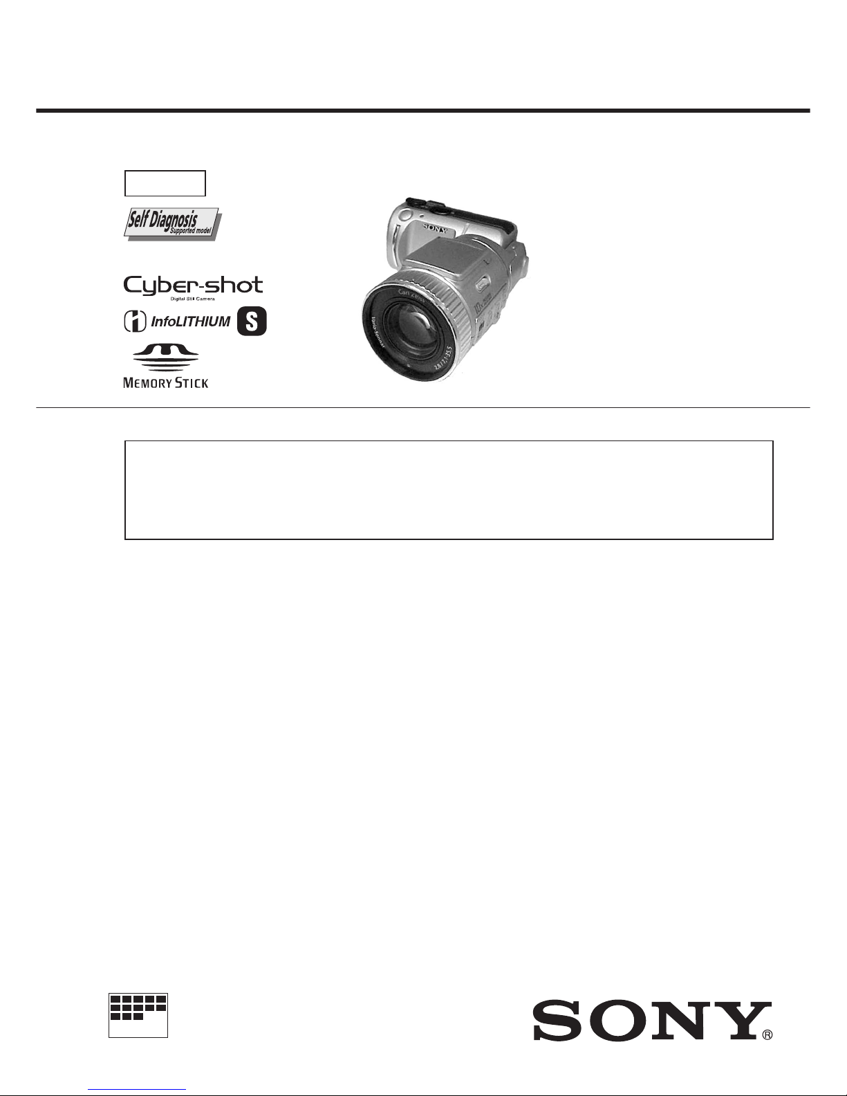
Sony DSC-F505,Cybershot DSC-F505 Service Manual
– 1 –
DSC-F505
US Model
Canadian Model
AEP Model
UK Model
E Model
Hong Kong Model
Australian Model
Chinese Model
Korea Model
Tourist Model
SERVICE MANUAL
DIGITAL STILL CAMERA
MICROFILM
Level 2
This service manual contains information for Japanese model as well.
SPECIFICA TIONS
System
Recording format
Digital (JPEG based)/Field
recording
Video signal
NTSC color, EIA standards
P AL color CCIR standards
Image device
1/2-inch CCD (total number
of square pixels : 1636 x 1236),
square grid, primary color filter
Interface format
Lens
ƒ = 7.1 - 35.5 mm (38 - 190 mm, when
converted into a 35 mm still camera)
0.5 m - ∞ (“W” side)
0.08 m - ∞ (Macro, “W” side)
F = 2.8 - 3.3
Photometric system
TTL system
Exposure control
Automatic exposure
White balance
Automatic, Indoor, Outdoor,
One-push
Data compression system
Movie : MPEG-1
Still : JPEG
Audio (with still image) :
MPEG AUDIO (Monaural)
Data format
Still : 1600 x 1200
1024 x 768
640 x 480
320 x 240 (E-mail)
Movie : 320 x 240, 160 x 112
Memory
“Memory stick”
Flash
Recording distance
limitations : 11 7/8 inches to 8 1/3 feet
(0.3 m to 2.5 m), automatic flash
control system
Shutter speed
NTSC : 1/8 - 1/725
P AL : 1/6 - 1/600
LCD screen
Screen size
2 inches
LCD panel
TFT
Total dot number
122,980 (559 x 220) dots
Input and output connectors
A/V out (Monaural)
Minijack
Video : 1Vp-p, 75 ohms,
unbalanced, sync negative
Audio : monaural, 327 mV
(at output, impedance more than
47 kilohms)
Output impedance with less than
2.2 kilohms
Digital I/O (serial)
Minijack
RS-232C based, 9.6 Kbps to
115.2 Kbps
Digital I/O (USB)
Special minijack
USB 1.0 based
General
Power consumption
Using the AC power
adaptor/charger :
Recording : 3.6 W
Playback : 3.1 W
Using the rechargeable
NP-FS11 lithium ion battery :
Recording : 3.3 W
Playback : 2.7 W
Operation temperature
32°F to 104°F (0°C to 40°C)
Storage temperature
-4°F to 140°F (-20°C to 60°C)
Dimensions
Approx. 4 1/4 x 2 1/2 x 5 3/8 in.
(107.2 x 62.2 135.9 mm)
(w / h / d)
Mass
Approx. 15 oz (435 g)
(excluding batteries)
Approx. 1 lb (475 g)
(including battery,
“Memory stick” (4 MB),
wrist strap and lens cap etc.)
AC-VF10 AC power adaptor/
charger
Power requirements
100 to 240 V AC, 50/60 Hz
Power consumption
13 W
Output voltage
DC OUT : 4.2 V, 1.8 A in operating
mode
Battery charge terminal :
4.2 V, 1.5 A in charge mode
Operation temperature
32°F to 104°F (0°C to 40°C)
Storage temperature
-4°F to 140°F (-20°C to 60°C)
Approx. 1 15/16 x 1 9/16 x 3 3/8 in.
(49 x 39 x 85 mm) (w / h / d)
Mass
Approx. 4.2 oz. (120 g)
(excluding batteries)
NP-FS11 battery pack
Voltage
DC 3.6 V
Capacity
4.1 Wh
Type
Lithium ion type
Design and specifications are subject
to change without notice.
On the PS-427, SY-56 board
This service manual provides the information that is premised the circuit
board replacement service and not intended repair inside the PS-427,
SY-56 board.
Therefore, schematic diagram, printed wiring board and electrical parts
list of the PS-427, SY-56 board are not shown.
The following pages are not shown.
PS-427 board
Schematic diagram ...............................Pages 4-15 to 4-18
Printed wiring board ..............................Page 4-11
Electrical parts list .................................Pages 6-12 to 6-13
SY-56 board
Schematic diagram ...............................Pages 4-23 to 4-33
Printed wiring board ..............................Pages 4-19 to 4-22
Electrical parts list .................................Pages 6-13 to 6-14
Ver 1.2 2000. 03
With SUPPLEMENT-1
(9-974-192-81)
– 2 –
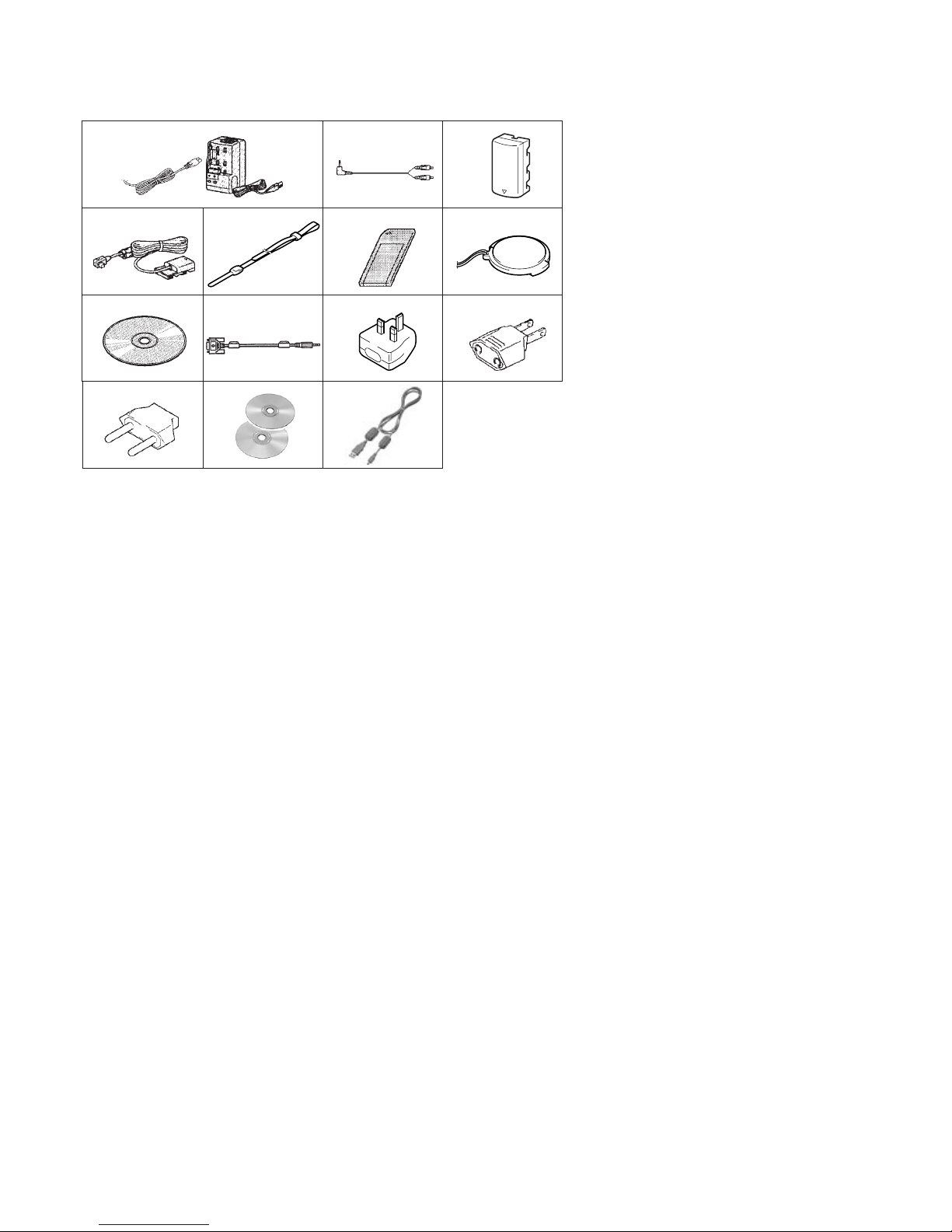
Supplied accessories
1 AC-VF10 AC power adaptor/charger,
Power cord (1)
2 A/V connecting cable (1)
3 NP-FS11 Battery pack (1)
4 DK-115 DC connecting cable (1)
5 Wrist strap (1)
6 Memory Stick (4MB) (1)
7 Lens cap/Lens cap strap (1)
8 Sony Picture Gear 3.2Lite (1)
(Compact Disk)
9 PC serial cable (1)
!º Conversion plug 3P adaptor (1)
UK, Hong Kong model
!¡ 2-pin conversion adaptor (1)
E model
!™ 2-pin conversion adaptor (1)
Tourist model
!£ USB driver software (1)
!¢ USB cable (1)
123
4567
89!º!¡
!™ !£ !¢
SAFETY-RELATED COMPONENT WARNING!!
COMPONENTS IDENTIFIED BY MARK ! OR DO TTED LINE WITH
MARK ! ON THE SCHEMATIC DIAGRAMS AND IN THE PARTS
LIST ARE CRITICAL TO SAFE OPERATION. REPLACE THESE
COMPONENTS WITH SONY PARTS WHOSE PART NUMBERS
APPEAR AS SHOWN IN THIS MANUAL OR IN SUPPLEMENTS
PUBLISHED BY SONY .
ATTENTION AU COMPOSANT AYANT RAPPORT
À LA SÉCURITÉ!
LES COMPOSANTS IDENTIFÉS P AR UNE MARQUE ! SUR LES
DIAGRAMMES SCHÉMA TIQUES ET LA LISTE DES PIÈCES SONT
CRITIQUES POUR LA SÉCURITÉ DE FONCTIONNEMENT. NE
REMPLACER CES COMPOSANTS QUE PAR DES PIÈSES SONY
DONT LES NUMÉROS SONT DONNÉS DANS CE MANUEL OU
DANS LES SUPPÉMENTS PUBLIÉS PAR SONY.
1. Check the area of your repair for unsoldered or poorly-soldered
connections. Check the entire board surface for solder splashes
and bridges.
2. Check the interboard wiring to ensure that no wires are
"pinched" or contact high-wattage resistors.
3. Look for unauthorized replacement parts, particularly
transistors, that were installed during a previous repair. Point
them out to the customer and recommend their replacement.
4. Look for parts which, through functioning, show obvious signs
of deterioration. Point them out to the customer and
recommend their replacement.
5. Check the B+ voltage to see it is at the values specified.
6. Flexible Circuit Board Repairing
• Keep the temperature of the soldering iron around 270˚C
during repairing.
• Do not touch the soldering iron on the same conductor of the
circuit board (within 3 times).
• Be careful not to apply force on the conductor when soldering
or unsoldering.
SAFETY CHECK-OUT
After correcting the original service problem, perform the following
safety checks before releasing the set to the customer.

– 3 –
TABLE OF CONTENTS
1. GENERAL ...................................................................1-1
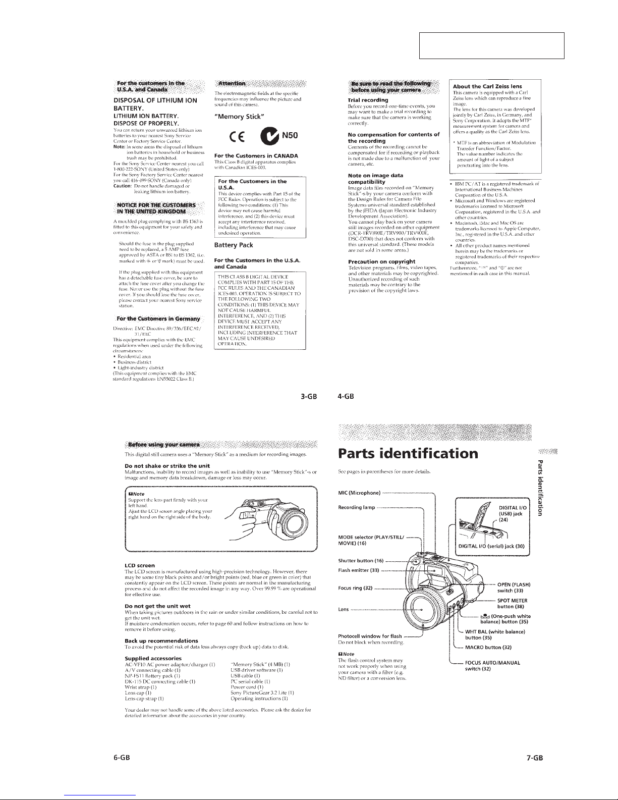
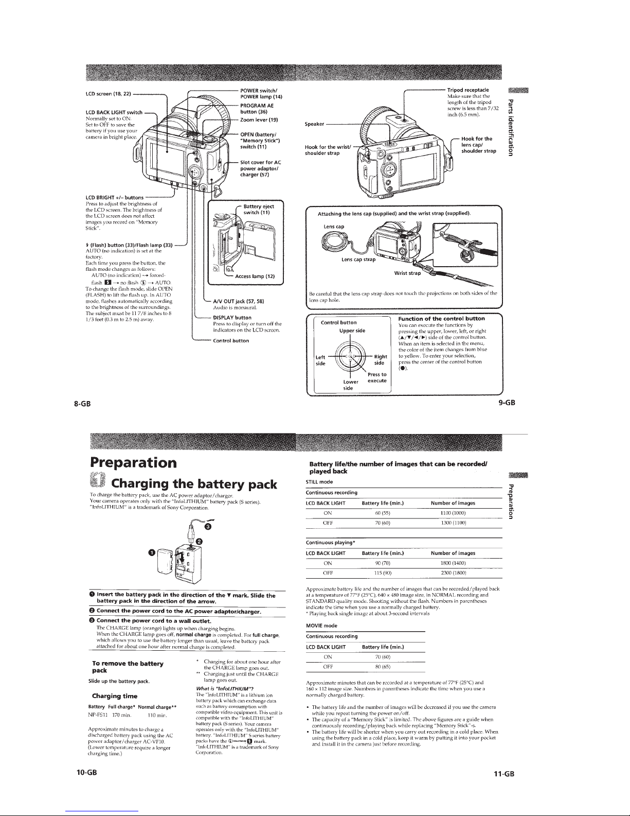
Parts identification.....................................................................1-1
Preparation.................................................................................1-2
1 Charging the battery pack and
“Memory Stick” ...........................................................1-2
2 Installing the battery pack ............................................1-3
3 Setting the date and time ..............................................1-3
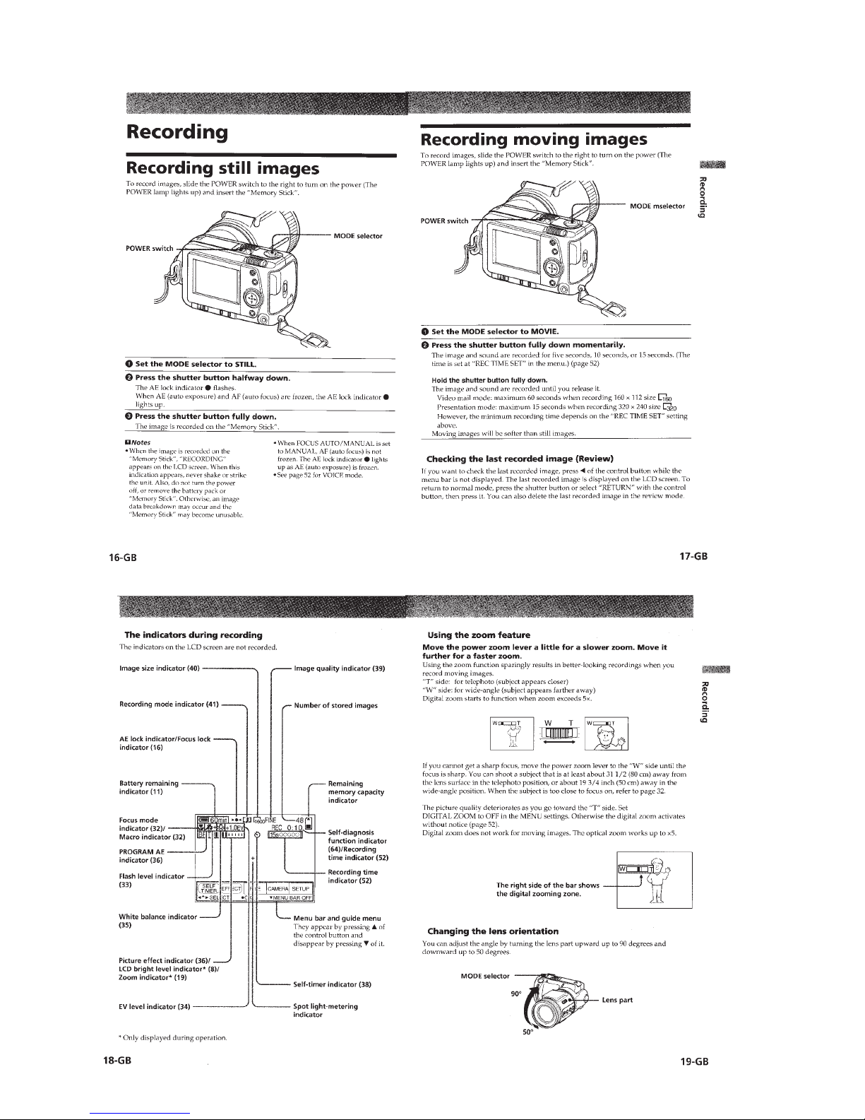
Recording ..................................................................................1-4
Recording still images .....................................................1-4
Recording moving images...............................................1-4
Playing back ..............................................................................1-5
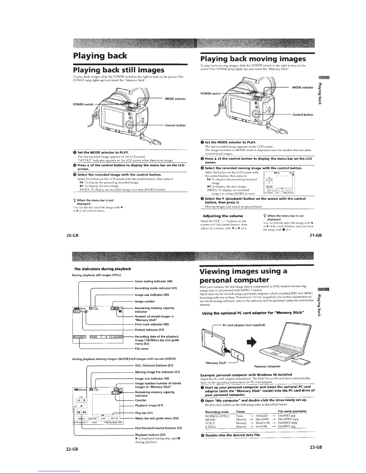
Playing back still images .................................................1-5
Playing back moving images...........................................1-5
Viewing images using a personal computer.................... 1-5
Various ways of recording .........................................................1-8
Various ways of playback ........................................................ 1-10
Changing the menu setting ......................................................1-13
Using image data with other equipment ..................................1-14
Additional information ............................................................1-15
2. DISASSEMBLY
• Attachiment of CPC-9 Jig .......................................................2-1
2-1. Removal of Rear Cabinet Block......................................2-2
2-2. Removal of Zoom Lens Block .......................................2-2
2-3 Removal of Cabinet (LT) Block ...................................... 2-3
2-4. Removal of Lens Block ..................................................2-3
• Service Positionn-1 (Lens Block Area : CD-236, LD-98,
PS-427 and SY-56 Boards)..............................................2-3
2-5. Removal of LCD Panel Block and
Control Switch Block (FK) .............................................2-4
• Service Positionn-2 (Rear Cabinet Area : LCD Panel and
Control Switch Block (FK)) ............................................2-4
2-6. Removal of HI-70, DD-131 Boards and
Battery Holder Block.......................................................2-5
2-7. Removal of Upper Cabinet Block and Flash Unit (MC) ...2-5
• Service Positionn-3 (HI-70 and DD-131 Boards) ................... 2-6
2-8. Removal of Front Cabinet Assembly...............................2-6
2-9. Removal and Attaciment of FP-133 Flexible Board .......2-7
2-10. To Fold the New FP-133 Flexible Board ........................2-7
2-11. Removal of Crystal Indication Module ...........................2-8
2-12. Removal of Flash Unit (ST).............................................2-8
2-13. Circuit Boards Location ..................................................2-9
2-14. Flexible Boards and Control Switch Block Location......2-9
3. BLOCK DIAGRAMS
3-1. Overall Block Diagram ...................................................3-1
4. PRINTED WIRING BOARDS AND
SCHEMATIC DIAGRAMS
4-1. Frame Schematic Diagram (1) ........................................4-3
Frame Schematic Diagram (2) ........................................4-5
4-2. Printed Wiring Boards and Schematic Diagram.............. 4-7
• CD-236 (CCD Imager, Camera)
Printed Wiring Board..............................................4-7
• CD-236 (CCD Imager, Camera)
Schematic Diagram.................................................4-9
• LD-98 (Lens Drive)
Printed Wiring Board............................................4-12
• MF UNIT
Schematic Diagram...............................................4-33
• CF/PW (Control Switch Block)
Schematic Diagram...............................................4-33
• HI-70 (LCD Drive, Timing Generator, V ideo,
Audio, Hi Control)
Printed Wiring Board............................................4-35
• HI-70 (LCD Drive)
Schematic Diagram...............................................4-39
• HI-70 (Timing Generator)
Schematic Diagram...............................................4-41
• HI-70 (Video)
Schematic Diagram...............................................4-43
• HI-70 (Audio)
Schematic Diagram...............................................4-45
• HI-70 (Hi Control (1/2) )
Schematic Diagram...............................................4-47
• HI-70 (Hi Control (2/2) )
Schematic Diagram...............................................4-49
• DD-131 (DC/DC Converter)
Printed Wiring Board............................................4-51
• DD-131 (DC/DC Converter)
Schematic Diagram...............................................4-53
• FK (Control Switch Block)
Schematic Diagram...............................................4-55
4-3. Waveforms..................................................................... 4-57
4-4. Printed Parts Location ................................................... 4-59

– 4 –
* The color reproduction frame is shown on page 141.
5. ADJUSTMENTS
1. Before starting adjustment...............................................5-1
1-1. Adjusting items when replacing main parts and boards.. 5-2
5-1. Adjustments..................................................................... 5-3
1-1. Preparations Before Adjustment......................................5-3
1-1-1.List of Service Tools........................................................5-3
1-1-2.Preparations .....................................................................5-4
1-1-3.Discharging of the strobe power supply..........................5-4
1-1-4.Precaution ........................................................................5-6
1. Setting the Switch............................................................5-6
2. Order of Adjustments ......................................................5-6
3. Subjects ...........................................................................5-6
4. Preparing the Flash Adjustment Box...............................5-7
1-2. Initialization of B, D, E, F, 7 Page Data ..........................5-8
1-2-1.Initialization of D Page Data ...........................................5-8
1. Initializing the D Page Data ............................................5-8
2. Modification of D Page Data...........................................5-8
3. D Page Table....................................................................5-8
1-2-2.Initializing the B, E, F, 7 Page Data .............................. 5-11
1. Initializing the B, E, F, 7 Page Data .............................. 5-11
2. Modification of B, E, F, 7 Page Data ............................5-11
3. F Page table ................................................................... 5-11
4. E Page Table ..................................................................5-14
5. B Page Table..................................................................5-16
6. 7 Page Table ..................................................................5-19
1-3. Video System Adjustments............................................5-21
1. Video Sync Level Adjustment.......................................5-21
(Control Switch Block (FK) )........................................5-21
2. Video Burst Level Adjustment ......................................5-21
(Control Switch Block (FK) )........................................5-21
3. Video Y Level Check..................................................... 5-21
(Control Switch Block (FK) )........................................5-21
1-4. Camera System Adjustments.........................................5-22
1. HALL Adjustment .........................................................5-22
2. Flange Back Adjustment (Using Minipattern Box).......5-23
3. Flange Back Adjustment ...............................................5-24
(Using Flange Back Adjustment Chart) ........................5-24
4. Flange Back Check........................................................5-24
5. Picture Frame Setting ....................................................5-25
6. F No. Standard Data Input.............................................5-25
7. Mechanical Shutter Adjustment ....................................5-26
8. AGC Standard Gain and Max Gain Adjustment ...........5-26
9. Light Level Adjustment and ND SHUTTER CHECK.. 5-26
10. Auto White Balance Standard Data Input .....................5-27
11. Auto White Balance ND Filter Compensation
Adjustment ....................................................................5-27
12. Auto White Balance Adjustment ...................................5-28
13. Color Reproduction Adjustment....................................5-29
13-1. Color Reproduction Adjustment (Without ND Filter)...5-29
13-2. Color Reproduction Adjustment (With ND Filter)........5-29
13-3. Color Reproduction Check ............................................5-30
14. White Balance Check ....................................................5-31
15. Strobe White Balance Adjustment ................................5-31
16. Strobe Light Level and White Balance Check ..............5-32
17. CCD Black Defect Compensation.................................5-32
18. CCD Black Defect Compensation Check .....................5-33
19. CCD White Defect Compensation ................................5-34
20. CCD White Defect Compensation Check .....................5-34
1-5. LCD SYSTEM ADJUSTMENT ...................................5-35
1. LCD Initial Data Input ..................................................5-35
2. VCO Adjustment (Control Switch Block (FK) )...........5-36
3. D Range Adjustment (Control Switch Block (FK) ) .....5-36
4. Bright Adjustment (Control Switch Block (FK) ).........5-37
5. Contrast Adjustment (Control Switch Block (FK) )......5-37
6. Color Adjustment (Control Switch Block (FK) ) ..........5-38
7. V-COM Level Adjustment (Control Switch Block
(FK) ) .............................................................................5-38
8. V -COM Adjustment....................................................... 5-39
9. White Balance Adjustment (HI-70 board).....................5-39
1-6. System Control System Adjustment..............................5-40
1. Battery End Adjustment (SY-54 board) .........................5-40
5-2. Service Mode.................................................................5-41
2-1. Adjustment Remote Commander ..................................5-41
1. Using the adjustment remote commander .....................5-41
2. Precautions upon using the adjustment remote
commander ....................................................................5-41
2-2. Data Process ..................................................................5-42
2-3. Service Mode.................................................................5-43
1. Setting the Test Mode ....................................................5-43
2. Bit value discrimination ................................................5-43
3. Switch check (1) ............................................................5-44
4. Switch check (2) ............................................................5-44
5. LED check .....................................................................5-44
5-3. System Control Adjustment...........................................5-45
1. Initializing the data of pages B, C, D, E, F, 7 ................5-45
2. Inputting the serial No. ..................................................5-45
2-1. Inputting the serial No. ..................................................5-45
6. REPAIR PARTS LIST
6-1. Exploded Views...............................................................6-1
6-1-1.Battery Holder Assembly ................................................6-1
6-1-2.Front Cabinet Assembly .................................................. 6-2
6-1-3.Rear Cabinet Assembly ...................................................6-3
6-1-4.Lens Cabinet Assembly...................................................6-4
6-1-5.Lens Assembly ................................................................6-5
6-2. Electrical Parts List .........................................................6-6
– 5 –
SERVICE NOTE
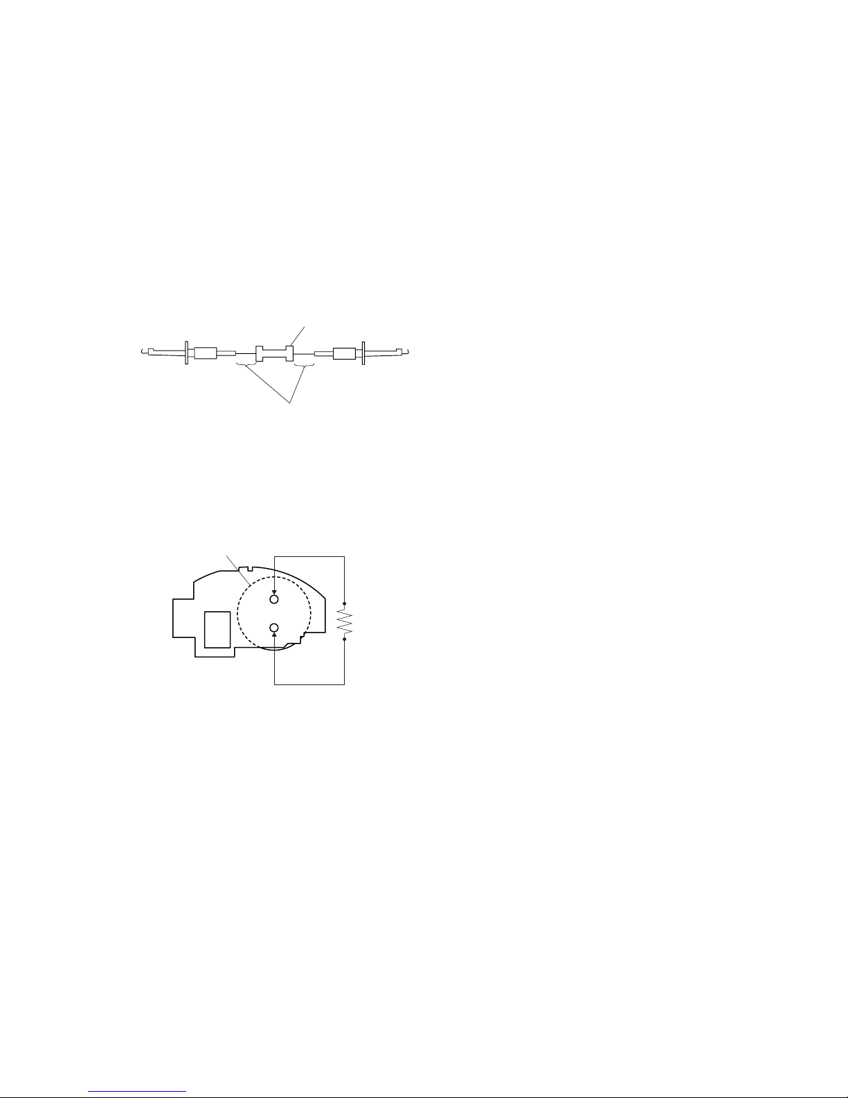
[Discharging of the FLASH unit’s charging capacitor]
The charging capacitor of the FLASH unit is charged up to the
maximum 300 V potential.
There is a danger of electric shock by this high voltage when the
capacitor is handled by hand. The electric shock is caused by the
charged voltage which is kept without discharging when the main
power of the DSC-F505 is simply turned off. Therefore, the
remaining voltage must be discharged as described below.
Preparing the Short Jig
To preparing the short jig. a small clip is attached to each end of a
resistor of 1kΩ /1W (1-215-869-11)
Wrap insulating tape fully around the leads of the resistor to prevent
electrical shock.
Discharging the Capacitor
Short circuits between the positive and the negative terminals of
charged capacitor with the short jig about 10 seconds.
1kΩ/1W
Wrap insulating tape.
Short ji
g
Capacitor
Flash unit (MC)
– 6 –
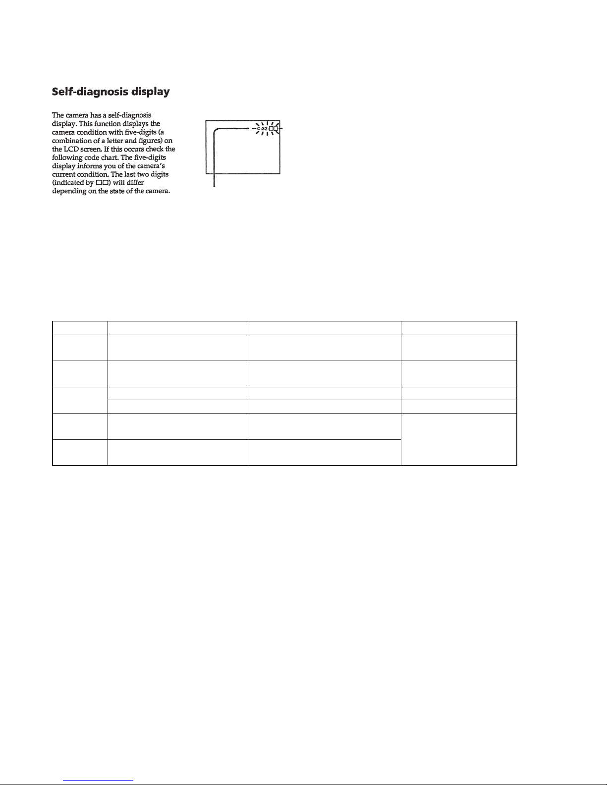
Note : The error code is cleared if the battery is removed, except defective
flash, unit.
*1 : The error display is given in two ways.
*2 : When the flash charging failed, Page:D, Address:C7, Data:04 are
written.
After repair, be sure to write Page:D, Address:C7, Data:00.
Self-diagnosis display
• C: ππ: ππ
You can reverse the camera
malfunction yourself. (However,
contact your Sony dealer or local
authorized Sony service facility
when you cannot recover from the
camera malfunction.)
• E: ππ: ππ
Contact your Sony dealer or local
authorized Sony service facility.
[Description on Self-diagnosis Display]
Display Code
C:04:ππ
C:32:ππ
C:13:ππ
E:61:ππ
E:91:ππ
Countermeasure
Use a NP-FS11/F10 battery pack.
Turn the power off and on again.
Format the “Memory stick”.
Insert a new “Memory Stick”.
Checking of lens drive circuit.
Cause
You are using a basttery pack that is not an
“InfoLITHIUM” battery pack.
Trouble with hardware.
Unformatted memory stick is inserted.
Memory stick is broken.
When failed in the focus and zoom
initialization.
Abnormality when flash is being
charged.
Checking of flash unit or replacement
of flash unit.
Caution Display During Error
for “InfoLITHIUM” BATTERY
ONL Y
SYSTEM ERROR
FORMAT ERROR
MEMORY STICK ERROR
—
*1
*2
1-1
DSC-F505
SECTION 1
GENERAL
This section is extracted from
instruction manual.
1-2

1-3
1-4
1-5
1-6
1-7

1-8
1-9
1-10
1-11
1-12
1-13

1-14
1-15E
2-1
SECTION 2
DISASSEMBLY
DSF-F505
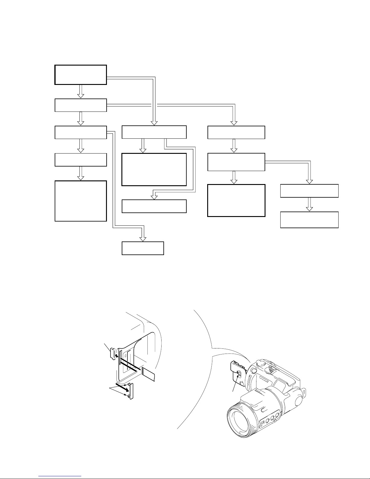
The equipment can be removed using the following procedure.
• ATTACHMENT OF CPC-9 JIG
START
2-1. REAR CABINET BLOCK
2-5. LCD PANEL BLOCK
CONTROL SWITCH BLOCK (FK)
2-11. CRYSTAL INDICATION MODULE
AND OTHER
ATTACHMENT OF CPC-9 JIG
AND
SERVICE POSITION-2
· LCD PANEL BLOCK
· CONTROL SWITCH BLOCK (FK)
ATTACHMENT OF CPC-9 JIG
AND
SERVICE POSITION-3
· HI-70 BOARD
· DD-131 BOARD
2-2. ZOOM LENS BLOCK
2-3. CABINET (LT) BLOCK
2-12. FLASH UNIT (ST)
2-4. LENS BLOCK
ATTACHMENT OF CPC-9 JIG
AND
SERVICE POSITION-1
· CD-236 BOARD
· LD-98 BOARD
· PS-427 BOARD
· SY-56 BOARD
2-6. HI-70 AND DD-131 BOARDS
BATTERY HOLDER BLOCK
2-7. UPPER CABINET BLOCK
CONTROL SW BLOCK (PW)
FLASH UNIT (MC)
2-8. FRONT CABINET ASSEMBLY
ABOUT FP-133 FLEXIBLE BOARD.
(Refer to 2-9. and 2-10.)
Control switch block (FK)
(CN002)
1
18
Note : Don't use the 12 pin flexible board of CPC-9 jig.
It causes damage to the unit
CPC cover
Slide the Release knob in the direction of arrow
A
.
To open the Battery lid.
Two claws
CPC-9 jig (J-6082-393-C)
(18p flexible board)
A
Release knob
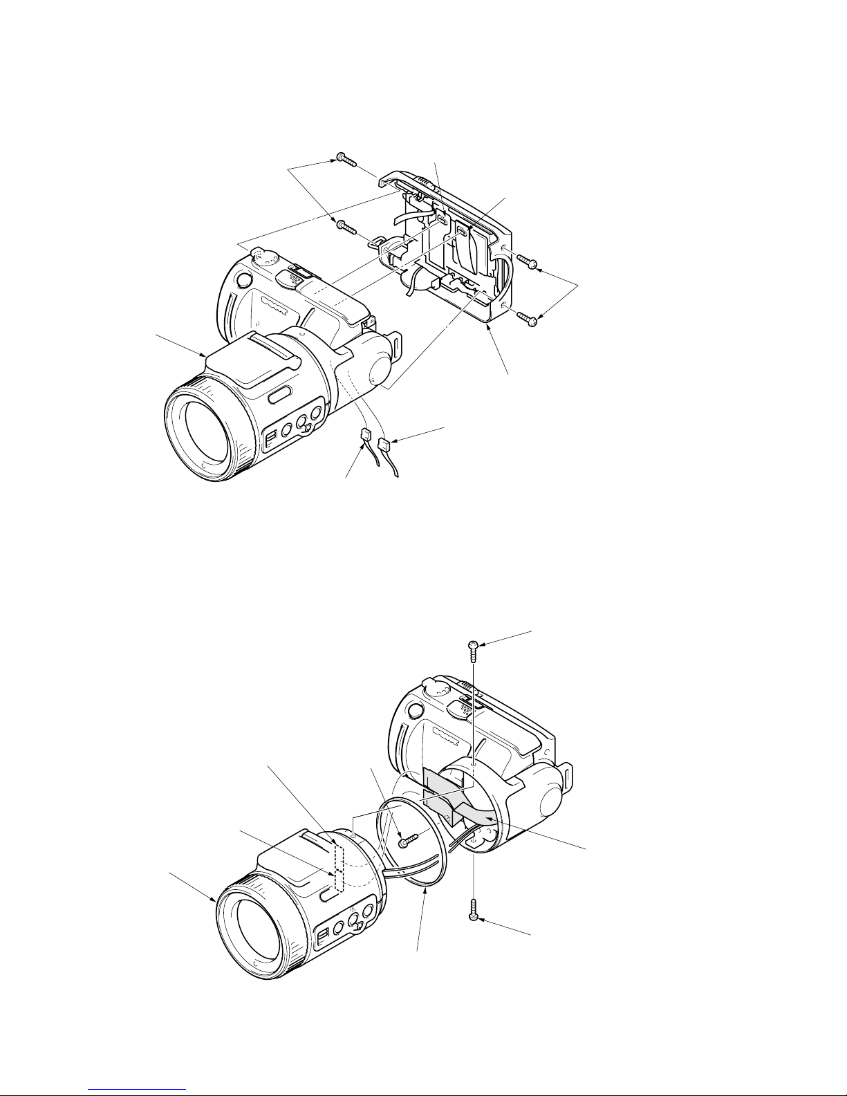
2-2
2-2. REMOVAL OF ZOOM LENS BLOCK
2-1. REMOVAL OF REAR CABINET BLOCK
FP-133 flexible boar
d
1
Screw (M1.7)
2
Screw (M1.7)
3
Screw (M1.7)
7
MF ornament
4
CN456
(SY-56 board)
5
CN455
(SY-56 board)
6
Zoom lens block
1
T wo screws
(M1.7)
5
Flexible board (Control switch block (FK))
(HI-70 board, CN607)
4
FP-134 flexible board
(HI-70 board, CN901)
3
Rear cabinet assembly
Front cabinet assembly
2
T wo screws
(M1.7)
6
Harness (HB-50)
(HI-70 board, CN605)
7
Harness (SP-163)
(HI-70 board, CN702)
NOTE : Follow the disassembly procedure in the numerical order given.
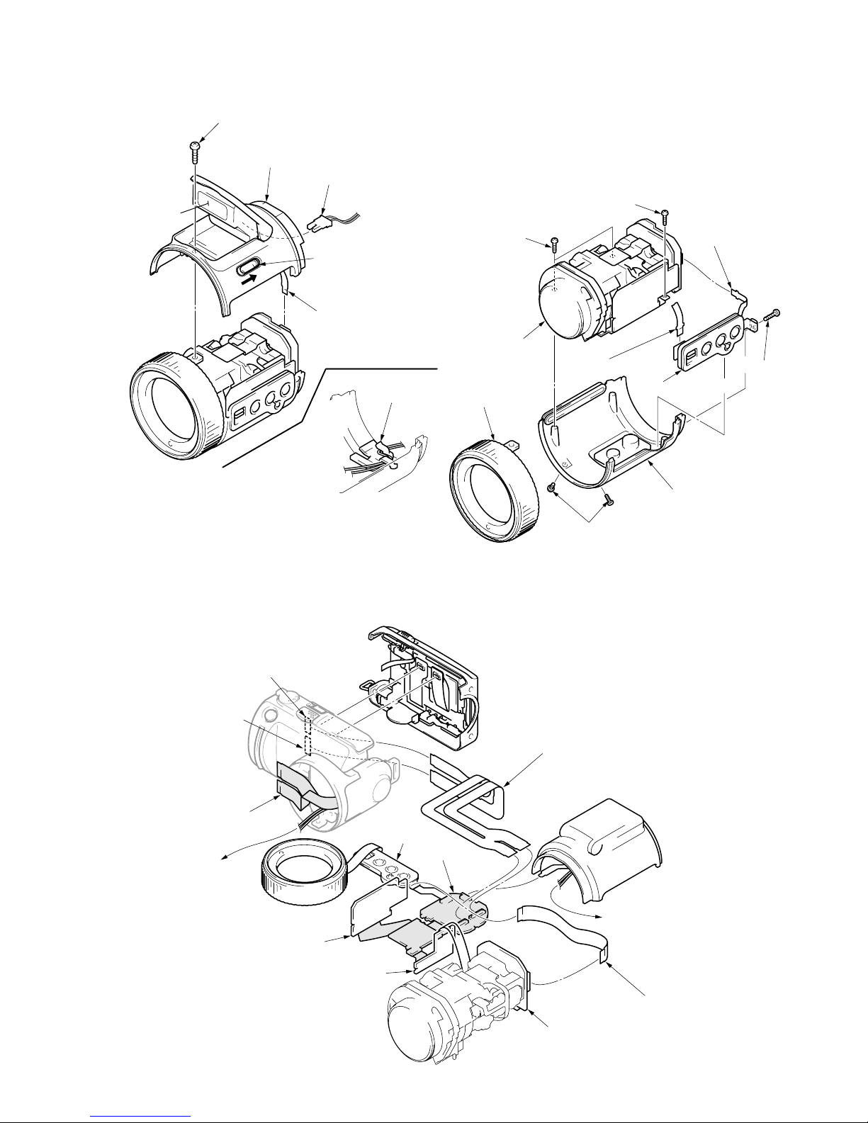
2-3
2
Screw (M1.7)
3
Cabinet (LT) block
1
Push the Release kno
b
4
FP-136 flexible board
(SY-56 board, CN454)
5
Harness (SM-114)
(Flash unit (ST), 2P)
(Note)
Flash unit
(Note)
Cabinet (LT) block
(Bottom view)
Harness clamp
2
CN453
(SY-56 board)
3
CN001
(Control switch block)
4
Control switch
block (CF)
5
T wo screws
(M1.7)
9
Cabinet (LB)
assembly
7
T wo screws
(M1.7)
8
Screw (M1.7)
1
Screw (M1.7
)
6
Cabinet (MF)
assembly
0
Lens block
2-3 REMOVAL OF CABINET (LT) BLOCK 2-4. REMOVAL OF LENS BLOCK
Extension cable (33, 39P 0.3 mm)
Parts No. : J-6082-447-A
(HI-70 board, CN602, 603)
(SY-56 board, CN455, 456)
Cabinet (LT) block
(Flash unit (ST))
Harness (MS-114)
(from Front cabinet block)
Cabinet (MF) assembly
Control switch block (CF)
LD-98 board
CD-236 board
PS-427 board
SY-56 board
Rear cabinet block
Lens block
Extension cable (39P 0.3 mm
)
Parts No. : J-6082-448-A
(PS-427 board, CN251)
(CD-236 board, CN101)
CN602
(HI-70 board)
CN603
(HI-70 board)
FP-133 flexible board
(Not used)
Harness (MS-114)
(to Cabinet (LT) block)
• SERVICE POSITION-1 (LENS BLOCK AREA : CD-236, LD-98, PS-427 and SY-56 BOARDS)
NOTE : Clamp the cables after attaching the Harness (MS-114). If
clamped with the flash unit closed, the flash unit cannot
be opened, Be sure to clamp the cable with the flash unit
opened.
2-4
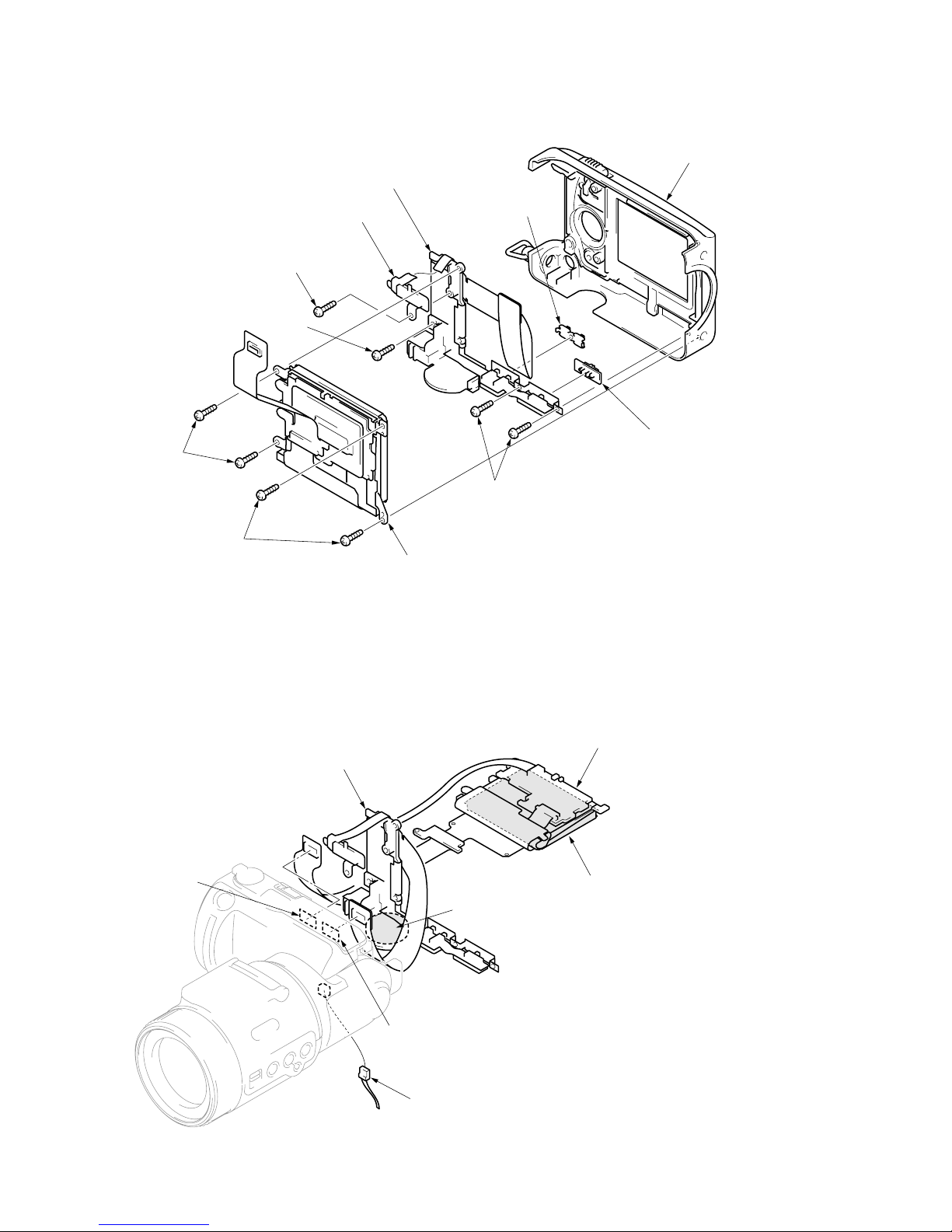
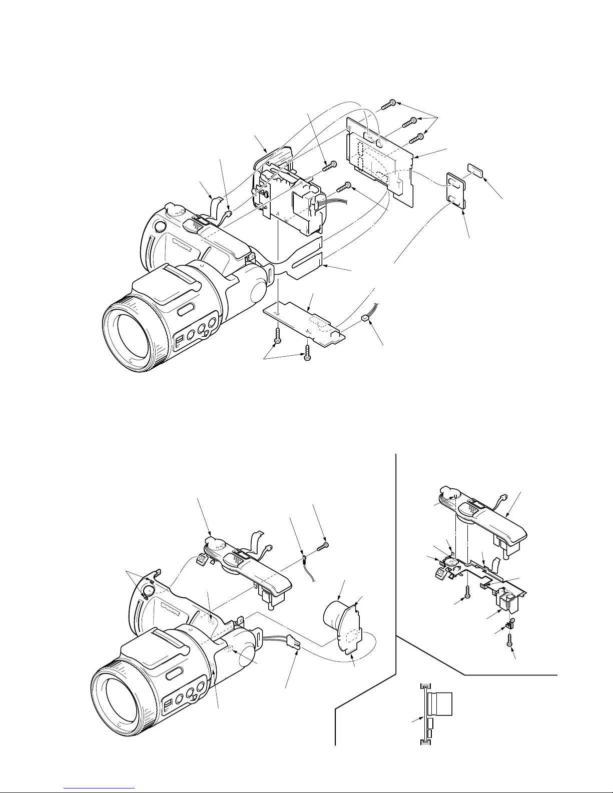
2-5. REMOVAL OF LCD PANEL BLOCK AND CONTROL SWITCH BLOCK (FK)
• SERVICE POSITION-2 (REAR CABINET AREA : LCD PANEL and CONTROL SWITCH BLOCK (FK))
Harness (From the SP901)
(HI-70 board, CN702)
Crystal indication module (LCD901)
(with FP-134 flexible board)
Control switch block (FK)
SP901
Cold cathode fluorescent tube (ND901)
(with Inverter transformer unit)
CN607
(HI-70 board)
CN901
(HI-70 board)
1
Screw (1.7 x 4)
6
Screw (M1.7)
5
LCD panel block
(Refer to 2-11. for details diagram on removal of LCD section)
3
T wo screws
(1.7 x 4)
4
Two screws (1.7)
7
Two screws (M1.7)
2
Zoom switch
(RV001)
8
Control switch block (FK)
Button (LCD bright)
Knob (LCD back light)
Rear cabinet assembly
2-5
2-6. REMOVAL OF HI-70, DD-131 BOARDS AND BATTERY HOLDER BLOCK
2-7. REMOVAL OF UPPER CABINET BLOCK AND FLASH UNIT (MC)
1
FP-132 flexible board
(HI-70 board, CN601)
(DD-131 board, CN003)
5
Three screws
(1.7 x 4)
!¡
T wo screws
(1.7 x 4)
8
Screw (M1.7)
0
Battery holder block
9
Screw
(M1.7)
!™
DD-131 board
6
HI-70 board
2
FP-133 flexible board
(HI-70 board, CN602,603)
3
Harness (Microphone)
(HI-70 board, CN701)
7
Harness (MD-97)
(DD-131 board, CN002)
4
Control switch block (PW)
(HI-70 board, CN604)
BB fixed sheet
Details diagram on removal and attachment
of Control switch block (PW)
Note for installation of
Flash unit (MC)
1
Screw (M1.7)
Screw (1.7 x 4)
Screw (1.7 x 4)
JK retainer assembly
Control switch block (PW)
5
Flash unit (MC)
(Note)
(Take note of claw B)
2
Harness (GN-52)
4
Harness (MS-114)
Two claws
A
3
Upper cabinet block
(Take note of two claws
A
)
Claw
Upper cabinet bloc
k
Hole
Claw
Claw
Pin
Claw
Groove
Groove
Groove
Groove
Edge
Edge
Should be fit to the Front
cabinet groove.
Flash unit (MC)
Claw
B
NOTE : When the flash unit (MC) charging failed, Page : D, Address : C7, Data : 04 are written.
After repair, be sure to write Page : D, Address : C7, Data : 00.
2-6
• SERVICE POSITION-3 (HI-70 and DD-131 BOARDS)
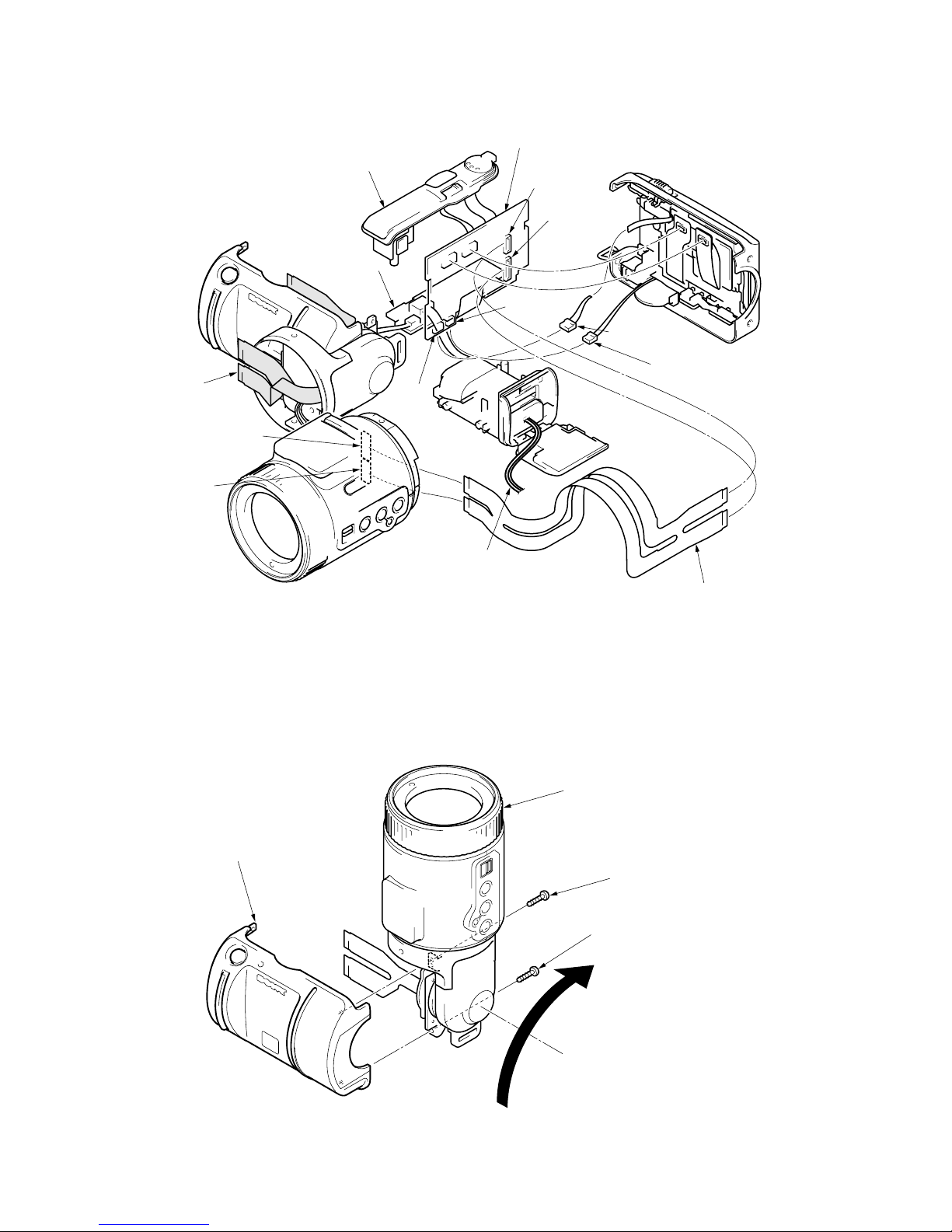
2-8. REMOVAL OF FRONT CABINET ASSEMBLY
1
Lift up the Zoom lens block.
4
Front cabinet assembly
3
Screw (M2 x 4)
2
Screw (M2 x 4)
Rear cabinet block
Front cabinet block
CN456
(SY-56 board)
FP-133 flexible board
(Not used)
CN602
CN603
CN702
CN605
Harness (HB-50)
Harness (SP-163)
CN455
(SY-56 board)
Zoom lens block
Control switch block (PW)
Battery holder block
(To AC power adaptor)
Extension cable (33, 39P 0.3 mm
)
Parts No. : J-6082-447-A
(HI-70 board, CN602, 603)
(SY-56 board, CN455, 456)
HI-70 board
DD-131 board
2-7
2-9. REMOVAL AND ATTACHIMENT OF FP-133 FLEXIBLE BOARD
Screw (M2 x 4)
Harness (GN-52)
FP holder
Harness (GN-52)
Harness (MS-114)
Harness (MS-114)
Harness (GN-52)
Hook the claw of harness
FP guard
Screw (M1.7)
Screw (M1.7)
Hook cover
Hinge cover
CN456
(SY-56 board)
CN455
(SY-56 board)
FP-133 flexible board
(33P side)
FP-133 flexible board
(39P side)
FP-133 flexible board
(33P side)
When attaching, coil in the direction of
arrow
A
with two and a half revolutions.
(FP-133 flexible board )
FP-133 flexible board
(39P side)
A
2-10. TO FOLD THE NEW FP-133 FLEXIBLE BO ARD
NOTE : For attaching new FP-133 flexible board, refer to “2-9.
Removal and attachment of FP-133 flexible board” .
FP-133
1-675-590-xx
FP-133
1-675-590-xx
: Fold
Adhesive tape
Adhesive tape
Adhesive tape
Adhesive tape
: Fold
NOTE : For folding new FP-133 flexible board, refer to “2-10. T o
fold the new FP-133 flexible board” .

2-8
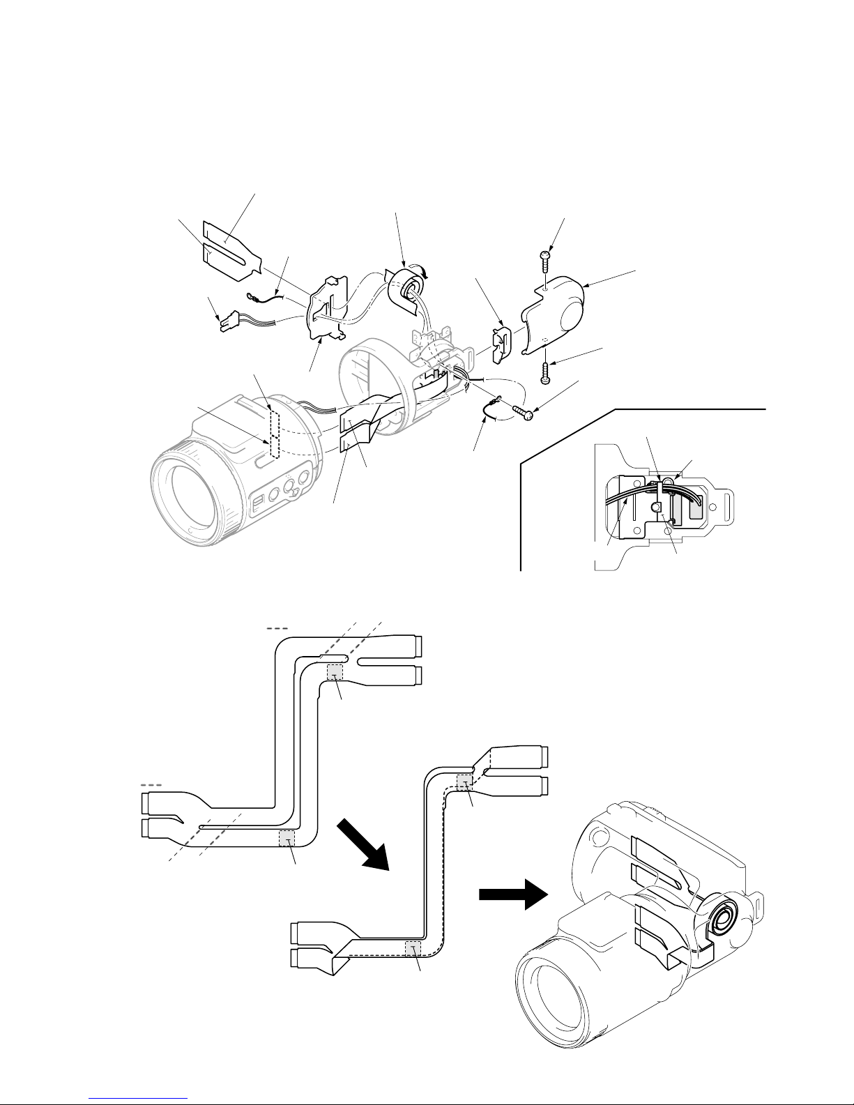
2-11. REMOVAL OF CRYSTAL INDICATION MODULE
2-12. REMOVAL OF FLASH UNIT (ST)
2
FP-136 flexible board
(Flash unit ST)
4
Cabinet (ST)
(Take note of four claws)
3
Push the Release knob
5
Flash unit (ST)
Claw
Claw
Claw
Claw
1
Screw
(M1.7 x 4)
1
Crystal indication module (LCD901)
(FP-134 flexible board, 24P)
5
Cold cathode fluorescent tube (ND901)
(Inverter transformer unit)
BL cushion
2
Screw (M1.7)
6
Inverter transformer unit
BL insulating sheet
4
Screw (M1.7)
3
FP-134 flexible board
BL light interception sheet
A
B
C
D
Note for installation
Portion
B
Portion
A
Portion C and
D
2-9
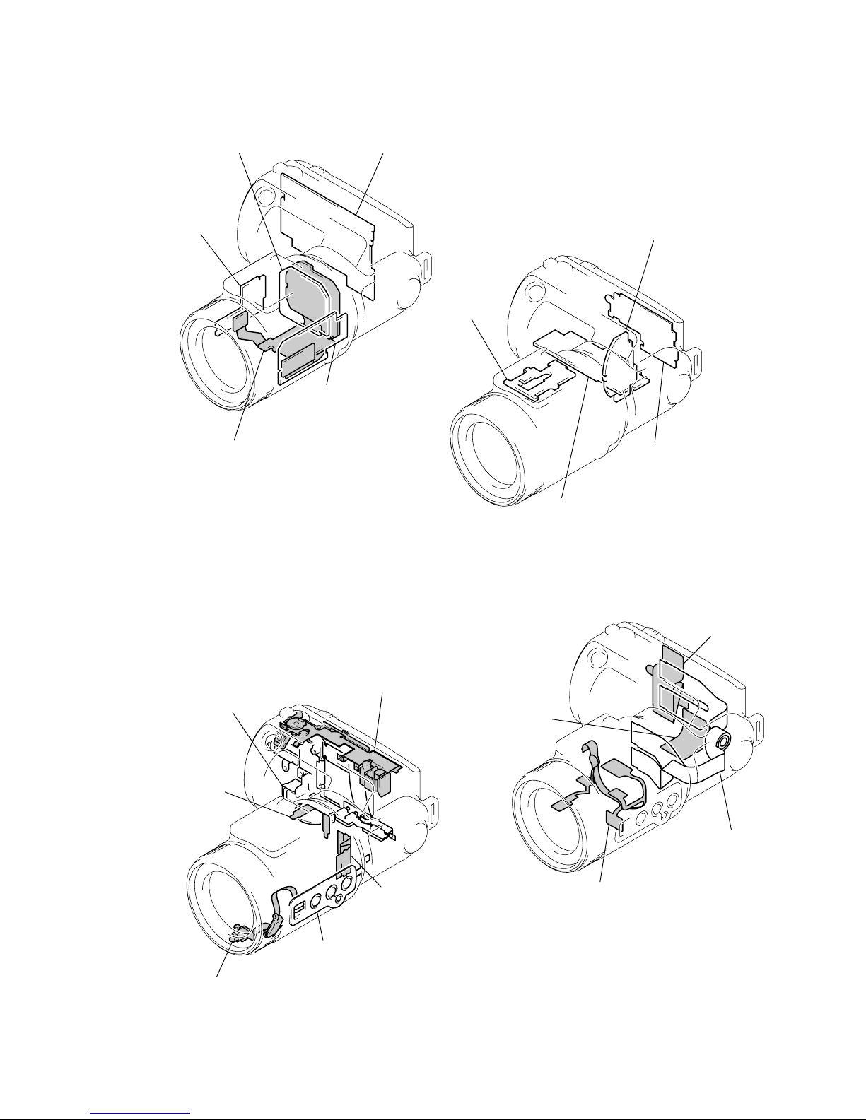
2-13. CIRCUIT BOARDS LOCATION
2-14. FLEXIBLE BOARDS AND CONTROL SWITCH BLOCK LOCATION
Flash unit (MC)
Flash unit (ST)
DD-131
(DC / DC Converter)
Inverter transformer uni
t
PS-427
(Camera DSP, Memory control)
LD-98
(Lens drive)
HI-70
(LCD drive, Timing generator, Video, Audio, HI control)
CD-236
(CCD imager, Camera)
SY-56
(SH DSP, Memory, Serial I / O, Connector, Digital I / O, )
Control switch block (CF)
Control switch block (FK)
FP-136
FP-135
Control switch block (PW)
Manual focus block
Lens block
FP-133
FP-132
FP-134
E
 Loading...