

Sony DPIF-4000 Service manual
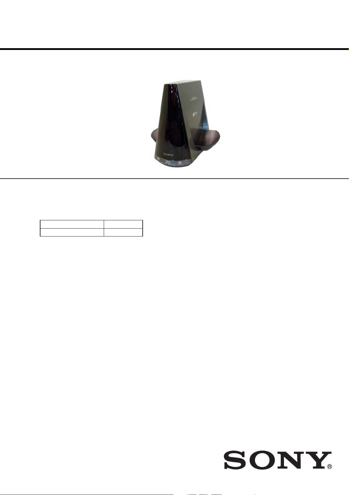
DP-IF4000
SERVICE MANUAL
Canadian Model
Ver. 1.1 2005. 02
• The DP-IF4000 is the digital surround
processor that comprises the MDR-DS4000.
* The digital surround processor for this system incorporates the Dolby Digital decoder, the Dolby Pro Logic II
decoder, the DTS decoder and the MPEG-2 AAC decoder.
Manufactured under licence from Dolby Laboratories and Digital Theater Systems, Inc.
“Dolby,” “Pro Logic,” the “AAC” logo and the double-D symbol are trademarks of Dolby Laboratories.
“DTS” and “DTS VIRTUAL ” are trademarks of Digital Theater Systems, Inc.
• MDR-DS4000 consists of the following models respectively.
Cordless stereo headphone MDR-IF4000
Digital surround processor DP-IF4000
US Model
AEP Model
E Model
SPECIFICATIONS
Decoder functions Dolby Digital
Virtual surround function
Compression function OFF
Modulation System DQPSK-IM
Secondary carrier wave frequency
Transmission distance Approx. 7 m (23 ft) to the front
Transmission range 12 – 24,000 Hz
Distortion rate 1% or less (1 kHz)
Audio inputs Optical input
Audio output Optical output (rectangular-type) x 1
Power requirements DC 9 V (from the supplied AC power
Dimensions Approx. 160 x 160 x 200 mm
Mass Approx. 400 g (15 oz)
Design and specifications are subject to change without notice.
Dolby Pro Logic II
DTS
MPEG-2 AAC
OFF
CINEMA
MUSIC
ON
3.75 MHz
(rectangular-type) x 1
Analogue input (pin jack left/right) x 1
adaptor)
(6 3/8 x 6 3/8 x 7 7/8 in) (w/h/d)
9-879-299-02
2005B02-1
© 2005.02
DIGITAL SURROUND PROCESSOR
Sony Corporation
Personal Audio Company
Published by Sony Engineering Corporation

DP-IF4000
Notes on chip component replacement
• Never reuse a disconnected chip component.
• Notice that the minus side of a tantalum capacitor may be
damaged by heat.
Unleaded solder
Boards requiring use of unleaded solder are printed with the lead
free mark (LF) indicating the solder contains no lead.
(Caution: Some printed circuit boards may not come printed with
the lead free mark due to their particular size.)
: LEAD FREE MARK
Unleaded solder has the following characteristics.
•Unleaded solder melts at a temperature about 40°C higher than
ordinary solder.
Ordinary soldering irons can be used but the iron tip has to be
applied to the solder joint for a slightly longer time.
Soldering irons using a temperature regulator should be set to
about 350°C.
Caution: The printed pattern (copper foil) may peel away if
the heated tip is applied for too long, so be careful!
• Strong viscosity
Unleaded solder is more viscous (sticky, less prone to flow)
than ordinary solder so use caution not to let solder bridges
occur such as on IC pins, etc.
• Usable with ordinary solder
It is best to use only unleaded solder but unleaded solder may
also be added to ordinary solder.
TABLE OF CONTENTS
Specifications ............................................................................ 1
1. GENERAL ................................................................... 3
2. DISASSEMBLY
2-1. Disassembly Flow ........................................................... 5
2-2. Cabinet (Lower), Luminous Window, IF Board .............. 5
2-3. TX Board ......................................................................... 6
3. ELECTRICAL ADJUSTMENT ............................. 7
4. DIAGRAMS
4-1. Block Diagrams ............................................................... 9
4-2. Printed Wiring Board – IF Board Section – .................... 10
4-3. Schematic Diagram – IF Board Section – ....................... 11
4-4. Printed Wiring Board – TX Board Section (Side A) – .... 12
4-5. Printed Wiring Board – TX Board Section (Side B) – .... 13
4-6. Schematic Diagram – TX Board Section (1/2) – ............ 14
4-7. Schematic Diagram – TX Board Section (2/2) – ............ 15
4-8. IC Pin Function Descriptions .......................................... 16
5. EXPLODED VIEWS
5-1. Processor Section ............................................................ 21
6. ELECTRICAL PARTS LIST .................................. 22
• Repaier DP-IF4000 with MDR-IF4000.
2
DP-IF4000
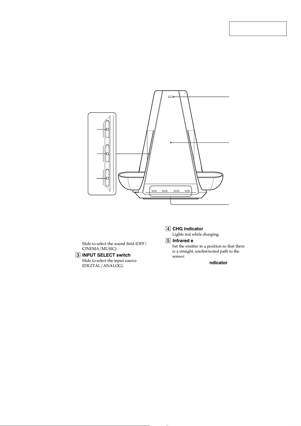
LOCATING THE CONTROLS
Front Panel of the Processor
3
2
INPUT SELECT
ANALOG DIGITAL
EFFECT
MUSIC OFF CINEMA
SECTION 1
GENERAL
This section is extracted
from instruction manual.
4
5
1
COMPRESSION
OFF ON
1 COMPRESSION switch
2 EFFECT switch
3 INPUT SELECT switch
6
4 CHG indicator
! " #!!
5 Infrared emitter
$ # #
# #!% & #
6 DECODE MODE indicator
3
DP-IF4000
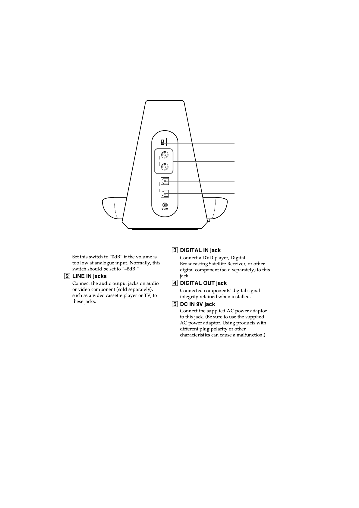
Rear Panel of the Processor
0dB
ATT
-
8dB
L
LINE IN
R
1
2
1 ATT (attenuator) switch
Set this switch to Ò0dBÓ if the volume is
too low at analogue input. Normally, this
switch should be set to ÒÐ8dB.Ó
2 LINE IN jacks
Connect the audio output jacks on audio
or video component (sold separately),
such as a video cassette player or TV, to
these jacks.
IN
DIGITAL
OUT
DC IN 9V
3 DIGITAL IN jack
Connect a DVD player, Digital
Broadcasting Satellite Receiver, or other
digital component (sold separately) to this
jack.
4 DIGITAL OUT jack
Connected components' digital signal
integrity retained when installed.
5 DC IN 9V jack
Connect the supplied AC power adaptor
to this jack. (Be sure to use the supplied
AC power adaptor. Using products with
different plug polarity or other
characteristics can cause a malfunction.)
3
4
5
4
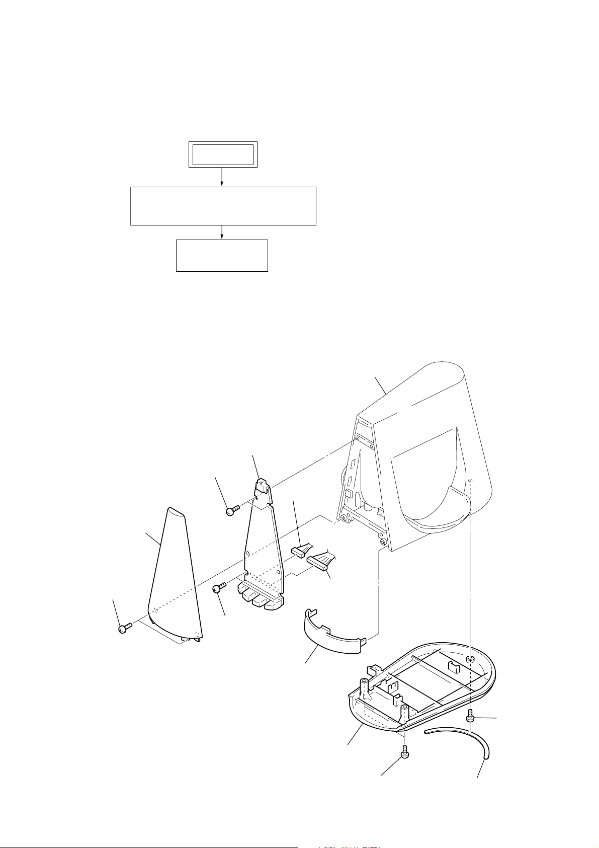
SECTION 2
DISASSEMBLY
• This set can be disassembled in the order shown below.
2-1. DISASSEMBLY FLOW
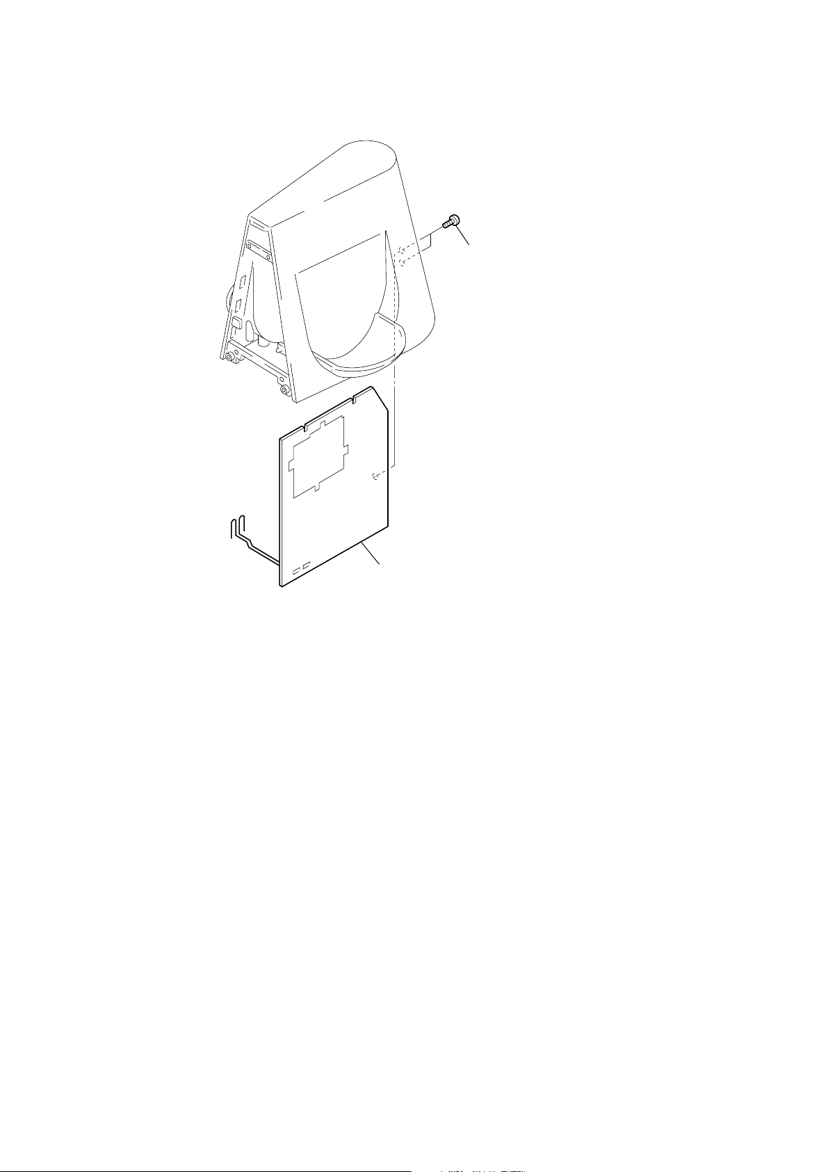
SET
2-2. CABINET (LOWER), LUMINOUS WINDOW,
IF BOARD
(Page 5)
2-3. TX BOARD
(Page 6)
Note: Follow the disassembly procedure in the numerical order given.
DP-IF4000
2-2. CABINET (LOWER), LUMINOUS WINDOW, IF BOARD
q;
IF board
8
two screws
(+B2.6)
qa
connector
(CN502)
7
luminous window
qs
connector
6
two screws (B2.6)
9
two screws
(+B2.6)
(CN501)
cabinet (upper)
5
indication window assy
4
cabinet (lower)
2
two screws (B2.6)
3
screw (B2.6)
1
rubber foot (back)
5
DP-IF4000
2-3. TX BAORD
1
two screws (B2.6)
2
TX board
6
SECTION 3
ELECTRICAL ADJUSTMENT
Note:
Feed 9V dc power supply voltage.
Set S502 INPUT SELECT to ANLOG side on feeding the power.
(In case of it goes to DIGITAL side, the RF signal is not out without
the optical input.)
Be sure to use an oscilloscope with the 200MHz bandwidth or more.
DP-IF4000
RF Level Adjustment
Connection:
Oscillscope
+
–
Adjustment method:
Connect an oscilloscope to each TP501, 502, 503, 504, 505, 506,
507, 508, 509 or 510 on IF board, adjust with RV601 on TX board
so that the output voltage goes to 1.10 ± 0.05 Vp-p.
TP501, 502, 503, 504, 505,
506, 507, 508, 509, 510
IF BOARD(SIDE A
TX BOARD
(
SIDE A
TP504
EE
Q501
TP501
TP509
Q518
TP507
TP505
Q505
TP502
Q502
)
506
EE
Q506
TP510
EE
Q519
TP508
EE
Q508
Q507
EE
Q504
Q503
TP503
1
CN501
10
1
CN502
7
)
RV601:RF LEVEL Adjustemnt
1
36
37
1
10
144
IC1201
72
73
109
108
IC1202
20
32
IC601
49
17
16
1
64
11
33
48
7
DP-IF4000
SECTION 4
DIAGRAMS
NOTE FOR PRINTED WIRING BOARDS AND SCHEMATIC DIAGRAMS.
For schematic diagrams.
Note:
• All capacitors are in µF unless otherwise noted. (p: pF) 50 WV or
less are not indicated except for electrolytics and tantalums.
• All resistors are in Ω and 1/4 W or less unless otherwise specified.
•%: indicates tolerance.
• f : internal component.
• C : panel designation.
• A : B+ Line.
• H : adjustment for repair.
• Power voltage is dc 9 V and fed with regulated dc power supply
from battery terminal.
•Voltages and waveforms are dc with respect to ground under nosignal conditions.
•Voltages are taken with a VOM (Input impedance 10 MΩ).
Voltage variations may be noted due to normal production tolerances.
•Waveforms are taken with a oscilloscope.
Voltage variations may be noted due to normal production tolerances.
• Circled numbers refer to waveforms.
• Signal path.
F : ANALOG
J : RF
c : DIGITAL
For printed wiring boards.
Note:
• X : parts extracted from the component side.
• f : internal component.
• : Pattern from the side which enables seeing.
• Indication of transistor.
C
Q
B
E
These are omitted.
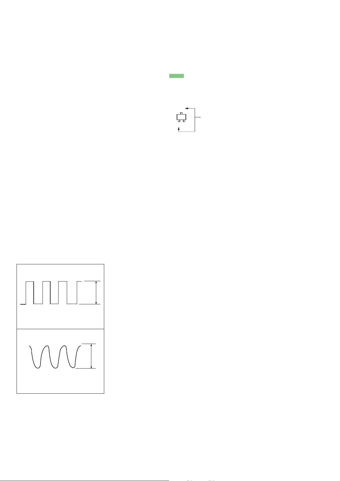
• Waveforms
– TX BOARD –
IC201
1
20V/DIV, 0.2 µsec/DIV
2
0.5V/DIV, 20 nsec/DIV
i;
5 MHz
IC601 OSCO
tl
24.567 MHz
XO
34.4Vp-p
2.2Vp-p
8
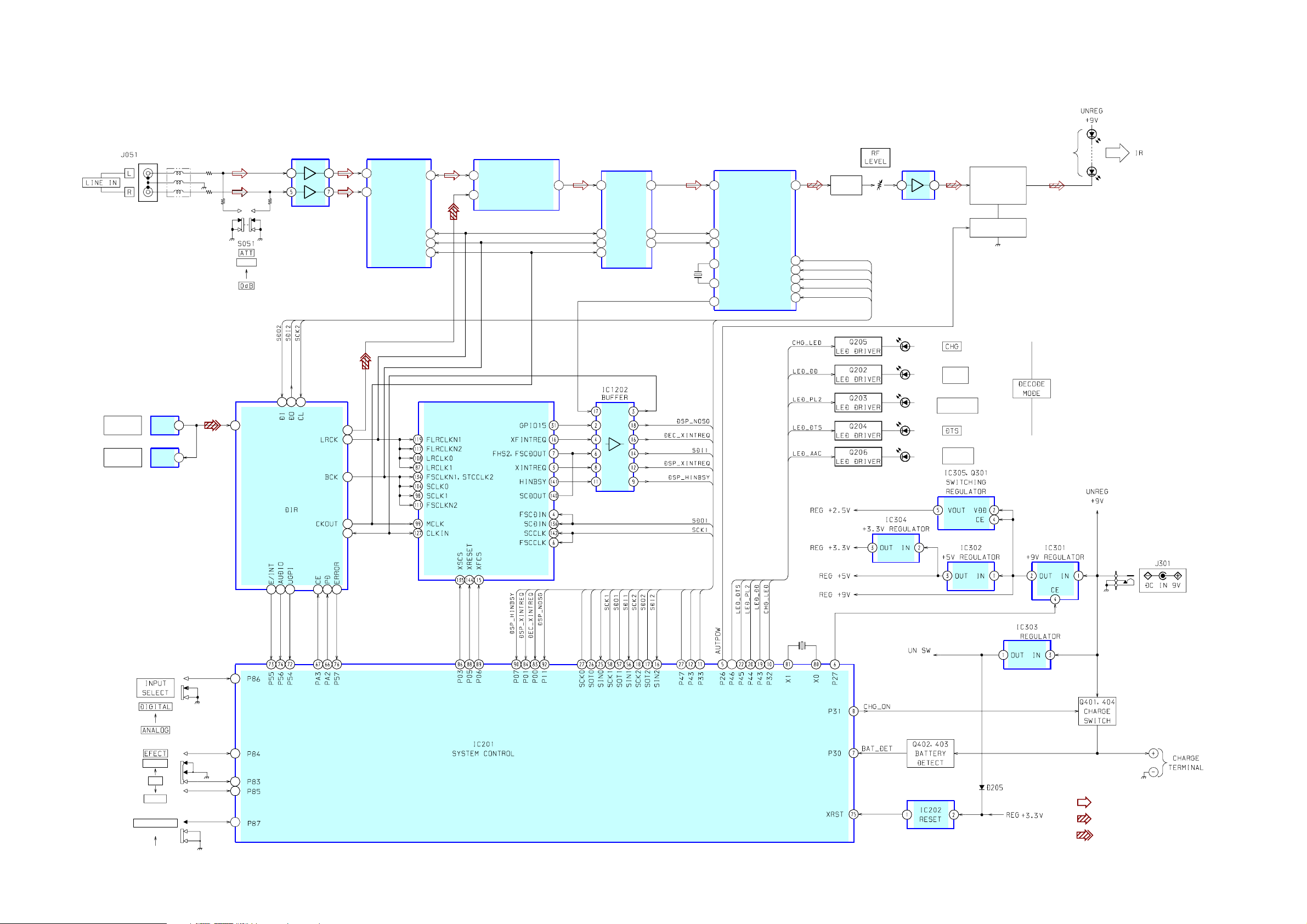
4-1. BLOCK DIAGRAM
DP-IF4000
DIGITAL
IN
DIGITAL
OUT
IC001
VOUT
IC004
VIN
LF051
LINE
FILTER
1
3
12
-8.5dB
RXIN
LINE AMP
786
IC052
DATAO
Q601
BUFFER
RV601
IC602
RF AMP
31
D521
DOLBY
D522
DIGITAL
DOLBY
D523
PRO LOGIG II
D524
MPEG-2
D525
AAC
Q501-512
Q518-520
LED DRIVER
Q514-517
DRIVE SWITCH
D505-520
D526-529
IC3
CONVERTER
831
LIN
SDATO
2
7
RIN
BCLK
3
12
LRCLK
13
MCLK
BCK
AUDIO DECODER/DSP
22
21
20
131
FSDATAN1
FSDATAN2
118
LRCK
IC1201 (2/2)
IC1201 (1/2)
VIRTUALIZER
DTO
DATA LATCH
2D
4D
1D
9
CLOCK
IC603
IC601
IR TRANSMITTER
/DSP
2Q
4Q
1Q
X601
24.576MHz
DTIN
5013 15
BCK
LRCK
494 2
OSCI
57
59
OSCO
CK12
53
DAAOUT
SWDT
SCLK
XSCEN
APS
XRST
2148110 5 7
15
13
14
41
64
SD02
SCK2
DIAT_XCS
DIATP_XRST
DIAT_XRST
S502
S501
CINEMA
OFF
MUSIC
S503
COMPRESSION
ON
OFF
IC2
19
24
XIN
9
11 5 3 2
10
DIAT_XRST
LED_AAC
23
X201
5.0MHz
+4.2V
+4.2V
• Signal Path
: ANALOG
: RF
: DIGITAL
DIAT_XCS
DIATP_XRST
54
52
51
53
55
DP-IF4000
99
DP-IF4000
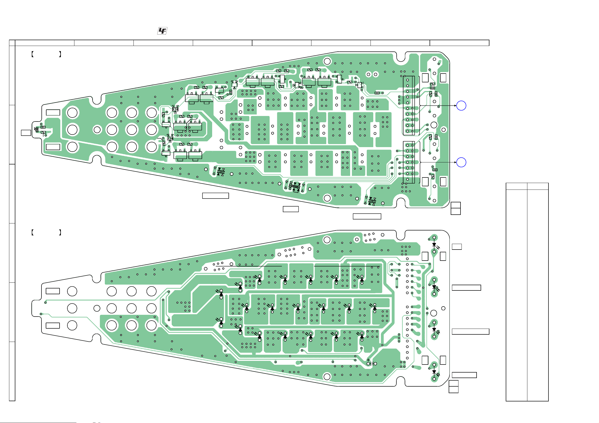
4-2. PRINTED WIRING BOARD – IF BOARD SECTION –
1
IF BOARD(SIDE A
)
2
A
D521
CHG
B
C511
R517
C
IF BOARD(SIDE B
)
D
: Uses unleaded solder.
3 4 5 6 7
R508
Q512
R518
E
Q520
E
Q517
R520
EE
Q516
R516
EE
Q508
R513
R514
EE
Q505
Q506
R519
Q519
Q518
R515
Q507
INPUT SELECT
DIGITAL T ANALOG
Q511
E
S502
R507
Q515
D528
E
C501
Q502
EE
D529
R510
Q501
E
R506
CINEMA T OFF t MUSIC
IR TRANSMITTER
D520
R509
Q509
S501
EFFECT
D516
R512
Q513
E
EE
Q504
R511
Q503
D512
E
Q510
R505
D508
Q514
E
C509
S503
COMPRESSION
ON T OFF
D519
10
8
1
CN501
1
CN502
7
R501
C516
R503
R504
C514
R502
1-864-942-
C513
C512
TX BOARD
A
Suffix-11
(
Page 13
TX BOARD
Suffix-12
(
Page 30
TX BOARD
B
Suffix-11
(
Page 13
TX BOARD
Suffix-12
(
Page 30
11
(11)
D524
DTS
D522
DOLBY DIGITAL
)
)
)
• Semiconductor Location
)
Ref. No. Location
D505 E-5
D506 E-6
D507 E-5
D508 D-6
D509 E-6
D510 E-7
D511 E-5
D512 D-6
D513 E-6
D514 E-6
D515 E-4
D516 D-5
D517 E-5
D518 E-6
D519 D-6
D520 D-5
D521 B-1
D522 E-8
D523 E-8
D524 D-8
D525 F-8
D526 E-4
D527 E-4
D528 E-4
D529 E-4
E
F
DP-IF4000
D527
D526
D515
D505
D511
1010
D517
D507
D513
D518
D509
D514
D506
C508
D510
1-864-942-
D523
DOLBY PRO LOGIC II
D525
MPEG-2 AAC
11
(11)
Q501 A-5
Q502 A-5
Q503 A-6
Q504 A-5
Q505 A-4
Q506 A-3
Q507 B-7
Q508 B-3
Q509 A-5
Q510 A-6
Q511 A-4
Q512 B-3
Q513 A-5
Q514 A-6
Q515 A-4
Q516 B-3
Q517 B-3
Q518 B-4
Q519 B-3
Q520 B-3
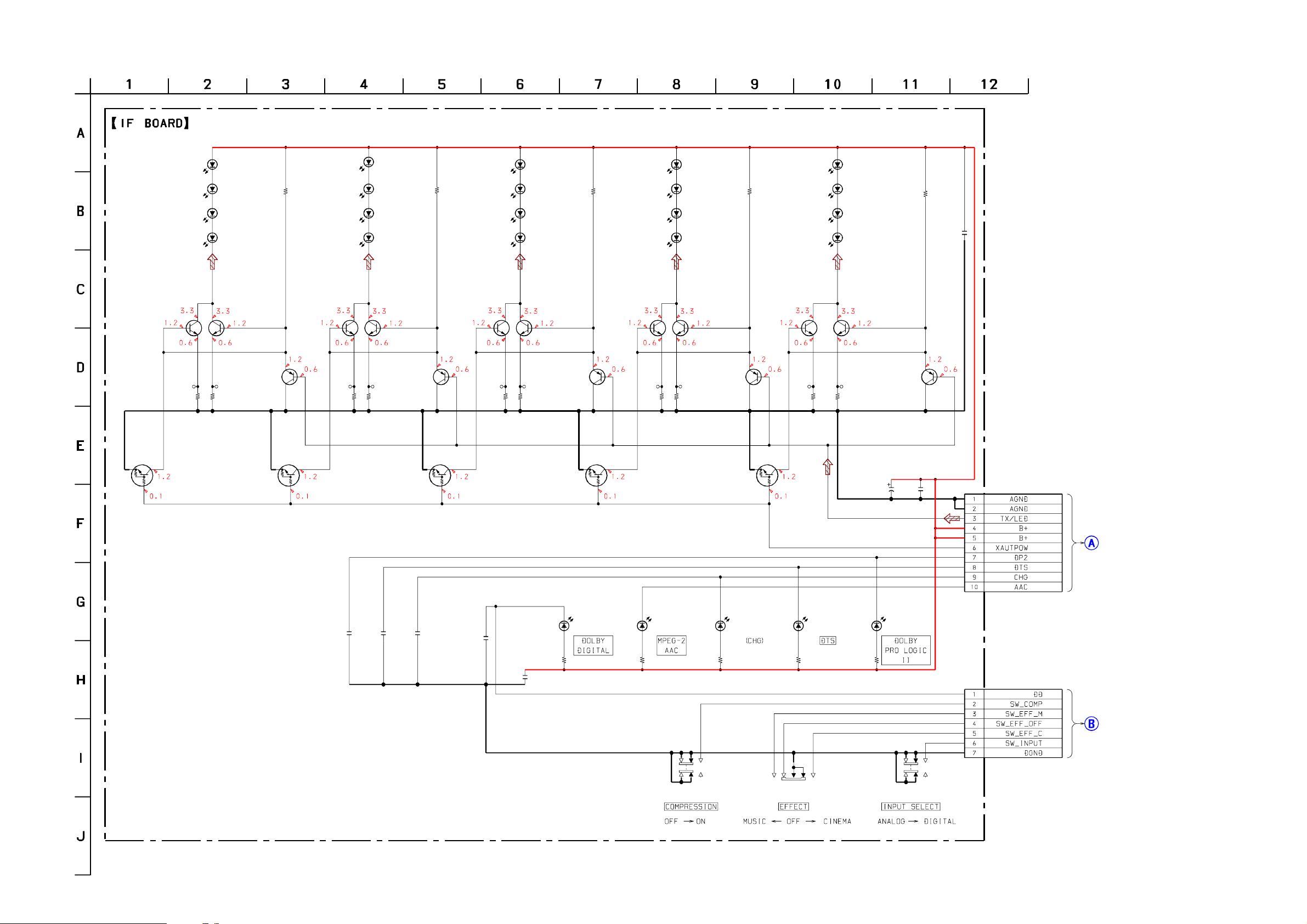
4-3. SCHEMATIC DIAGRAM – IF BOARD SECTION –
DP-IF4000
D506-520,526-529
IR TRANSMITTER
D506
DAL5821
D509
DAL5821
D513
DAL5821
D517
DAL5821
Q501
2SD1615A-GP
LED DRIVE
TP501
R509
12
Q502
2SD1615A-GP
LED DRIVE
Q509
2SA1037AKT146Q
LED DRIVE
TP502
R510
12
R506
2.2k
D505
DAL5821
D510
DAL5821
D514
DAL5821
D518
DAL5821
Q503
2SD1615A-GP
LED DRIVE
TP503
R511
12
Q504
2SD1615A-GP
LED DRIVE
Q510
2SA1037AKT146Q
LED DRIVE
TP504
R512
12
R505
2.2k
DAL5821
DAL5821
DAL5821
DAL5821
Q505
2SD1615A-GP
LED DRIVE
TP505
R513
D507
D511
D515
D519
12
Q506
2SD1615A-GP
LED DRIVE
Q511
2SA1037AKT146Q
LED DRIVE
TP506
R514
12
R507
2.2k
D508
DAL5821
D512
DAL5821
D516
DAL5821
D520
DAL5821
Q507
2SD1615A-GP
LED DRIVE
TP507
R515
12
Q508
2SD1615A-GP
LED DRIVE
Q512
2SA1037AKT146Q
LED DRIVE
TP508
R516
12
Q517
DTC143TUA-T106
DRIVE SWITCH
R508
2.2k
D526
DAL5821
D527
DAL5821
D528
DAL5821
D529
DAL5821
Q518
2SD1615A-GP
LED DRIVE
TP509
R519
12
R520
R518
2.2k
C501
0.1
Q519
2SD1615A-GP
LED DRIVE
Q520
2SA1037AKT146Q
LED DRIVE
TP510
12
C508
C509
100
0.1
16V
CN501
10P
Q513
DTC143TUA-T106
DRIVE SWITCH
Q514
DTC143TUA-T106
DRIVE SWITCH
C513
0.001
C514
0.001
DTC143TUA-T106
C511
0.001
Q515
DRIVE SWITCH
C512
0.001
C516
0.001
R504
560
Q516
DTC143TUA-T106
DRIVE SWITCH
D522
SLI-325URC
R501
1k
D525
SLI-325URC
S503
R517
560
D521
SLI-325URC
R502
1k
S501
D524
SLI-325URC
R503
560
D523
SLI-325URC
S502
CN502
7P
TX
BOARD
(2/2)
Suffix-11
(Page15)
TX
BOARD
(2/2)
Suffix-11
(Page15)
TX
BOARD
(2/2)
Suffix-12
(Page32)
TX
BOARD
(2/2)
Suffix-12
(Page32)
DP-IF4000
1111
DP-IF4000
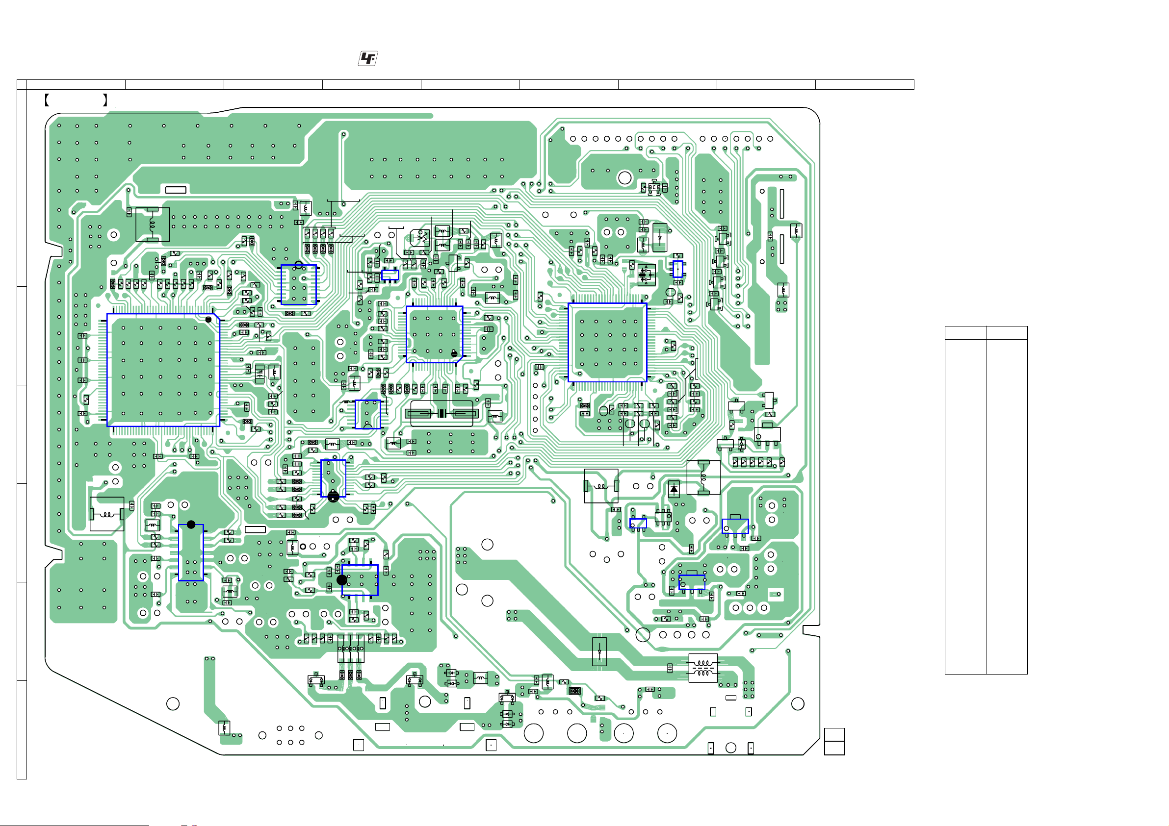
4-4. PRINTED WIRING BOARD – TX BOARD SECTION (SIDE A) –
1
TX BOARD(SIDE A
2
)
A
L1203
C1221
B
R1253
L1208
L1209
R1254
37
C
C1214
C1215
R1245
R1244
C1211
R1243
R1240
R1238
R1235
R1236
L1207
C1209
R1233
136
R1228
R1252
144
R1251
R1227
L1206
L1210
C1203
IC1201
C1216
C1217
D
E
F
G
R1249
L1204
72
C1210
C1222
C075
L051
R068
R065
C072
C069
IC3
718
C068
C1208
14
109
10873
R066
R067
C070
L052
C074
L060
3 4 5 6 7
C1224
R014
L008
R1256
C005
C008
R017
L007
L006
C064
R058
R059
L009
L005
R055
D052
L1205
20
13
R013
R053
R630
R1220
R1219
R1217
R1216
R1255
C1205
C1202
L1202
R1202
L611
C1207
R023
R022
R021
R024
C1218
1
10
C1220
C1204
C056
R057
L1211
R1215
L1201
C1206
R1214
C1201
C009
R020
L056
IC1202
L003
24
IC2
C078
C077
C052
R051
R1258
R1259
R1260
L1215
R616
L1212
C615
C627
C625
C015
12
1
R061
C059
C066
85
14
C060
R062
LF051
L055
L054
: Uses unleaded solder.
R1257
C610
R614
C612
C613
54
1113
R623
C622
R622
R625
C624
R627
L612
L608
L607
R010
C002
R069
C057
C609
R634
R613
33
48
L609
C629
C628
RV601
C620
IC601
R628
L1213
L1214
C611
R618
R633
9
16
IC603
R004
R005
R009
C623
L606
R060
R617
IC602
C621
R624
L610
R629
8
1
IC052
R063
24
C051
R054
R052
R056
D051
L053
R615
R621
C630
D057
D056
L602
C619
C631
X601
L603
C608
R620
R619
C632
E
1732
6449
C607
Q601
C604
16
1
C633
R612
C618
11
R609
C603
R631
C606
C605
R610
L062
R632
D054
R611
L605
C601
L601
L604
D055
D053
C634
C616
C001
C211
R267
C014
L002
R002
1
25
L201
C209
L001
C207
100
R224
C208
L303
D301
R001
R229
C210
IC201
SL204
C316
C216
C224
R220
R210
C222
C217
L202
R273
76
75
51
5026
R222
SL202
C223
R223
54
1
3
IC305
C003
Q205
D205
X201
SL203
C212
R228
R221
SL201
C206
Q301
31
46
R301
C221
R271
135
4
C226
R206
R236
R276
R274
C203
D302
C315
IC303
13
C308
C303
IC202
C205
R275
C204
R269
C201
R270
C202
Q402
C301
LF301
Q204
C219
E
Q203
C225
E
Q206
C218
E
Q202
C220
E
Q403
R408
E
L301
IC304
13
C310
R402
C305
E
D401
R403
C311
R404
8
L401
C401
L402
Q404
E
R409
Q401
E
R405
R406
R407
C312
1-864-940-
9
• Semiconductor Location
Ref. No. Location
D051 F-4
D052 F-3
D053 G-5
D054 G-5
D055 G-5
D056 G-5
D057 F-5
D205 B-7
D301 F-6
D302 D-7
D401 D-8
IC2 D-4
IC3 E-2
IC052 F-4
IC201 C-6
IC202 B-7
IC303 E-7
IC304 E-8
IC305 E-7
IC601 C-5
IC602 B-4
IC603 D-4
IC1201 C-2
IC1202 B-3
Q202 B-7
Q203 B-8
Q204 C-7
Q205 A-7
Q206 B-8
Q301 E-7
Q401 D-8
Q402 D-8
Q403 D-8
Q404 D-8
Q601 B-5
11
(11)
DP-IF4000
1212
 Loading...