

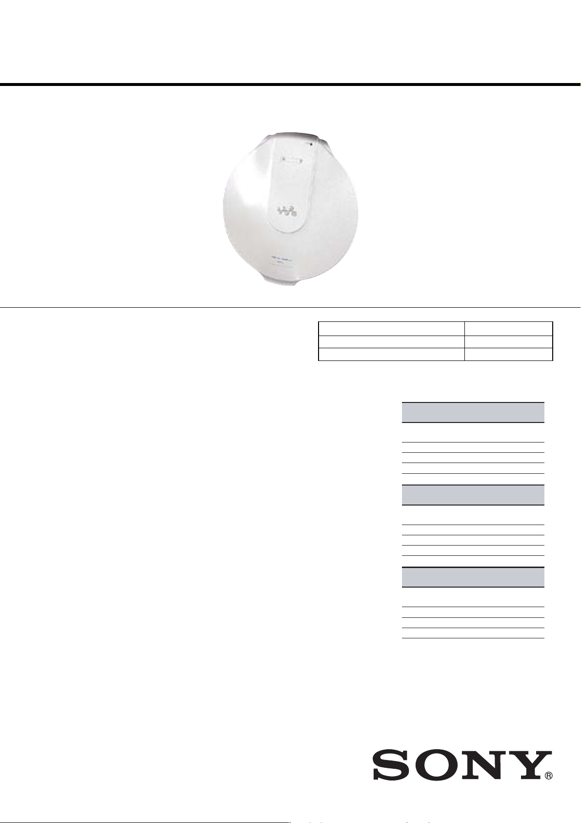
D-NE10
SERVICE MANUAL
Ver 1.2 2004.03
Manufactured under license from Dolby Laboratories
Licensing Corporation.
SPECIFICATIONS
US Model
Canadian Model
AEP Model
UK Model
E Model
Australian Model
Chinese Model
Tourist Model
Model Name Using Similar Mechanism NEW
CD Mechanism Type CDM-3325ER2
Optical Pick-up Name DAX-25E
System
Compact disc digital audio system
Laser diode properties
Material: GaAlAs
Wavelength: λ = 770 - 800 nm
Emission duration: Continuous
Laser output: Less than 44.6 µW
(This output is the value measured at a distance
of 200 mm from the objective lens surface on
the optical pick-up block with 7 mm aperture.)
D-A conversion
1-bit quartz time-axis control
Frequency response
20 - 20 000 Hz
Output (at 3 V input level)
Line output (stereo minijack)
Output level 0.7 V rms at 47 kΩ
Recommended load impedance over 10 kΩ
Headphones (stereo minijack)
Approx. 5 mW + Approx. 5 mW at 16 Ω
(Approx. 1.5 mW + Approx. 1.5 mW at 16 Ω )*
*For the customers in Europe
Optical digital output (optical output connector)
Output level: –21 - –15 dBm
Wavelength: 630 - 690 nm at peak level
+1–2
dB (measured by JEITA)
Power requirements
• Sony NH-14WM rechargeable battery:
1.2 V DC × 1
• LR6 (size AA) battery: 1.5 V DC × 1
•AC power adaptor (DC IN 3 V jack):
220 V, 50 Hz (Model for China)
120
V, 60 Hz (Model for Me
220-240 V AC 50/60 Hz
(Model for Saudi Arabia)
120 V, 60 Hz
(Models for US, Canadian and Taiwan)
230 V, 50 Hz
(Models for UK and Hong Kong)
100-240 V, 50 Hz
(Models for AEP, Tourist, E18, Korean and
East Europe)
Battery life*1 (approx. hours)
When you use the CD player on a flat and stable
surface.
When LIGHT mode and SOUND mode are set to
“OFF.”
Playing time varies depending on how the CD
player is used.
When using one NH-14WM (charged for about
2
)
5 hours*
G-PROTECTION
“G-PRO 1” “G-PRO 2”
Audio CD 20 20
ATRAC CD*
MP3 CD*
When using external battery case (one
alkaline battery*
Audio CD 30 30
ATRAC CD*
MP3 CD*
When using one NH-14WM and external
battery case (one alkaline battery*
Audio CD 50 50
ATRAC CD*
MP3 CD*
3
4
3
4
3
4
35 35
28 28
5
)
G-PROTECTION
“G-PRO 1” “G-PRO 2”
50 50
40 40
5
G-PROTECTION
“G-PRO 1” “G-PRO 2”
85 85
70 70
— Continued on next page —
)
9-961-304-03
2004C16-1
© 2004.03
PORTABLE CD PLAYER
Sony Corporation
Personal Audio Company
Published by Sony Engineering Corporation
D-NE10
*1 Measured value by the standard of JEITA (Japan
Electronics and Information Technology
Industries Association)
*2 Charging time varies depending on how the
rechargeable battery is used.
*3 Recorded at 48 kbps
*4 Recorded at 128 kbps
*5 When using Sony alkaline battery LR6 (SG)
(produced in Japan)
Operating temperature
5°C - 35°C (41°F - 95°F)
Dimensions (w/h/d) (excluding
projecting parts and controls)
Approx. 127 × 17.7 × 132.7 mm
23
⁄
32
× 5 1⁄4 in.)
(5 ×
Mass (excluding accessories)
Approx. 148 g (5.3 oz.)
Supplied accessories
AC power adaptor (1)
Rechargeable battery (1)
Battery carrying case (1)
Headphones/earphones (1)
Remote control (1)
Charging stand (1)
Carrying pouch (1)
External battery case (1)
CD-ROM* (SonicStage Simple Burner) (1)
User’s guide for SonicStage Simple Burner
US and foreign patents licensed from Dolby
Laboratories.
Design and specifications are subject to change
without notice.
(1)
This appliance is classified as a CLASS 1 LASER product.
The CLASS 1 LASER PRODUCT MARKING is located on
the rear exterior.
TABLE OF CONTENTS
1. SERVICING NOTE ·························································· 3
2. GENERAL ·········································································· 5
3. DISASSEMBLY ································································ 6
3-1. UPPER LID (SUB) ASSY ············································ 7
3-2. LIGHT GUIDE LENS··················································· 8
3-3. CABINET (INNER)······················································ 8
3-4. MAIN BOARD,
CD MECHANISM DECK (CDM-3325ER2) ···············9
3-5. TURN TABLE MOTOR ASSY (M901),
SLED MOTOR ASSY (M902),
OPTICAL PICK-UP (DAX-25E)································ 10
4. ELECTRICAL CHECKING········································· 11
5. DIAGRAMS······································································ 12
5-1. BLOCK DIAGRAM
– MAIN SECTION -1 – ·············································· 13
– MAIN SECTION -2 – ·············································· 14
– POWER SECTION – ··············································· 15
5-2. PRINTED WIRING BOARDS
– MAIN BOARD (SIDE A) – ···································· 16
5-3. PRINTED WIRING BOARDS
– MAIN BOARD (SIDE B) – ···································· 17
5-4. SCHEMATIC DIAGRAMS
– MAIN BOARD (1/4) –············································ 18
5-5. SCHEMATIC DIAGRAMS
– MAIN BOARD (2/4) –············································· 19
5-6. SCHEMATIC DIAGRAMS
– MAIN BOARD (3/4) –············································ 20
5-7. SCHEMATIC DIAGRAMS
– MAIN BOARD (4/4) –············································ 21
5-8. IC PIN FUNCTION DESCRIPTIONS ······················· 23
CAUTION
Use of controls or adjustments or performance of procedures
other than those specified herein may result in hazardous
radiation exposure.
Flexible Circuit Board Repairing
•Keep the temperature of the soldering iron around 270 ˚C dur-
ing repairing.
• Do not touch the soldering iron on the same conductor of the
circuit board (within 3 times).
• Be careful not to apply force on the conductor when soldering
or unsoldering.
Notes on chip component replacement
•Never reuse a disconnected chip component.
• Notice that the minus side of a tantalum capacitor may be dam-
aged by heat.
On AC power adaptor
•Use only the AC power adaptor supplied or
recommeded in “Accessories (supplied/
optional).” Do not use any other AC power
adaptor. It may cause a malfunction.
Polarity of the plug
6. EXPLODED VIEWS ······················································ 28
7. ELECTRICAL PARTS LIST·······································31
Unleaded solder
Boards requiring use of unleaded solder are printed with the leadfree mark (LF) indicating the solder contains no lead.
(Caution: Some printed circuit boards may not come printed with
the lead free mark due to their particular size.)
: LEAD FREE MARK
Unleaded solder has the following characteristics.
• Unleaded solder melts at a temperature about 40°C higher than
ordinary solder.
Ordinary soldering irons can be used but the iron tip has to be
applied to the solder joint for a slightly longer time.
Soldering irons using a temperature regulator should be set to
about 350°C.
Caution: The printed pattern (copper foil) may peel away if the
heated tip is applied for too long, so be careful!
• Strong viscosity
Unleaded solder is more viscous (sticky , less prone to flow) than
ordinary solder so use caution not to let solder bridges occur such
as on IC pins, etc.
• Usable with ordinary solder
It is best to use only unleaded solder but unleaded solder may
also be added to ordinary solder.
2
SECTION 1
2
IC601 FOK output ygpin
MAIN BOARD (SIDE B)
SERVICING NOTE
D-NE10
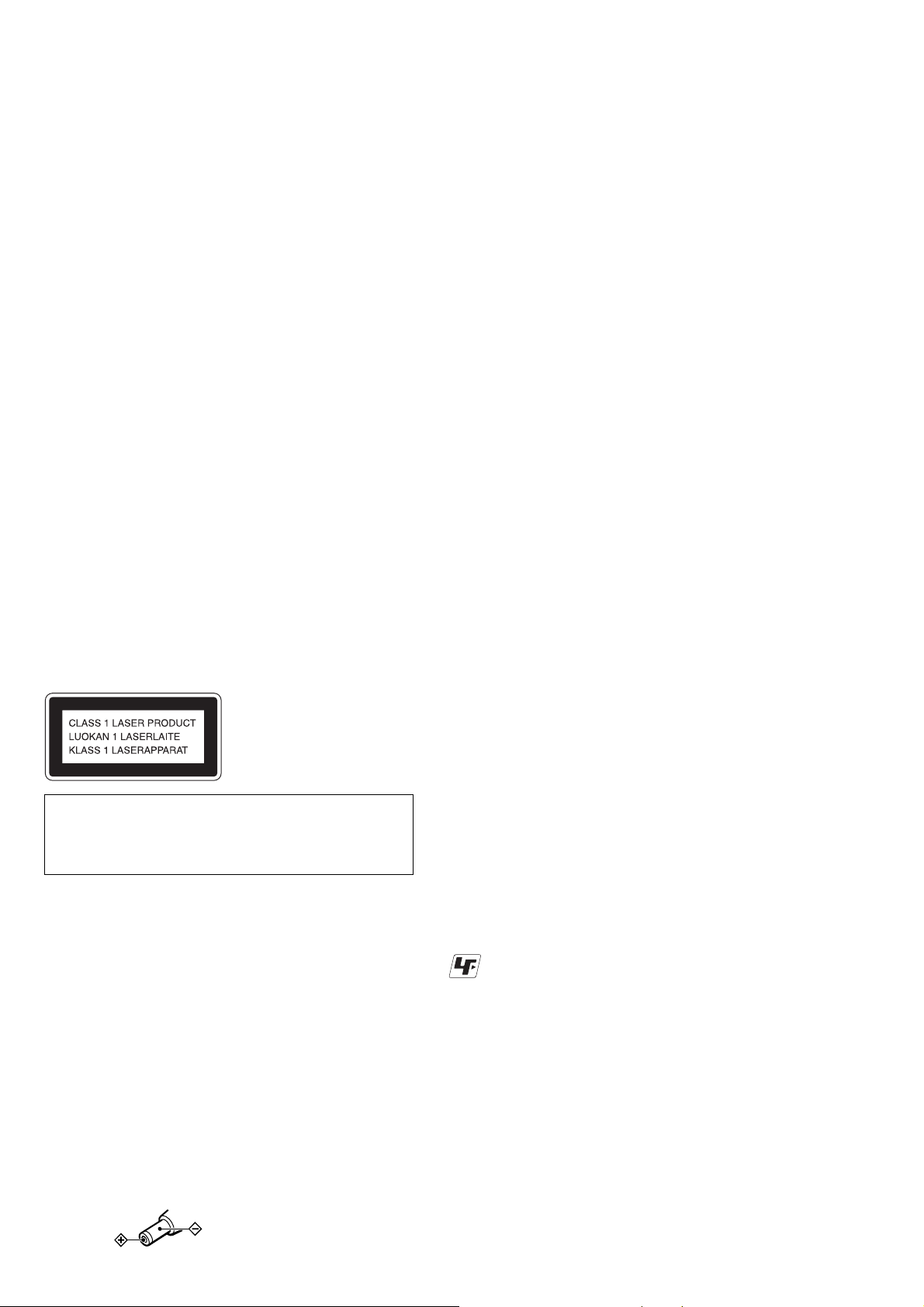
NOTES ON HANDLING THE OPTICAL PICK-UP
BLOCK OR BASE UNIT
The laser diode in the optical pick-up block may suffer electrostatic
breakdown because of the potential difference generated by the
charged electrostatic load, etc. on clothing and the human body.
During repair, pay attention to electrostatic breakdown and also use
the procedure in the printed matter which is included in the repair
parts.
The flexible board is easily damaged and should be handled with
care.
NOTES ON LASER DIODE EMISSION CHECK
The laser beam on this model is concentrated so as to be focused on
the disc reflective surface by the objective lens in the optical pickup block. Therefore, when checking the laser diode emission,
observe from more than 30 cm away from the objective lens.
SAFETY-RELATED COMPONENT WARNING!!
COMPONENTS IDENTIFIED BY MARK 0 OR DOTTED LINE WITH
MARK 0 ON THE SCHEMATIC DIAGRAMS AND IN THE PARTS
LIST ARE CRITICAL TO SAFE OPERATION. REPLACE THESE
COMPONENTS WITH SONY PARTS WHOSE PART NUMBERS
APPEAR AS SHOWN IN THIS MANUAL OR IN SUPPLEMENTS
PUBLISHED BY SONY .
BEFORE REPLACING THE OPTICAL PICK-UP BLOCK
Please be sure to check thoroughly the parameters as par the “Optical
Pick-Up Block Checking Procedures” (Part No.: 9-960-027-11)
issued separately before replacing the optical pick-up block.
Note and specifications required to check are given below.
• FOK output: IC601 yg pin
When checking FOK, remove the lead wire to disc motor.
• RF signal P-to-P value: 0.45 to 0.65 Vp-p
LES COMPOSANTS IDENTIFÉS P AR UNE MARQUE 0 SUR LES
DIAGRAMMES SCHÉMA TIQUES ET LA LISTE DES PIÈCES SONT
CRITIQUES POUR LA SÉCURITÉ DE FONCTIONNEMENT. NE
REMPLACER CES COMPOSANTS QUE PAR DES PIÈSES SONY
DONT LES NUMÉROS SONT DONNÉS DANS CE MANUEL OU
DANS LES SUPPÉMENTS PUBLIÉS PAR SONY.
ATTENTION AU COMPOSANT AYANT RAPPORT
À LA SÉCURITÉ!
LASER DIODE AND FOCUS SEARCH OPERATION
CHECK
During normal operation of the equipment, emission of the laser
diode is prohibited unless the upper lid is closed while turning ON
the S812.
The following checking method for the laser diode is operable.
• Method:
Emission of the laser diode is visually checked.
1. Remove the upper lid.
2. With a disc not set, turn on the S812 with a screwdri ver having a
thin tip as shown in Fig.1.
3. Press the u button.
4. Observing the objective lens, check that the laser diode emits
light.
When the laser diode does not emit light, automatic power control
circuit or optical pickup is faulty.
In this operation, the objective lens will move up and down 4
times along with inward motion for the focus search.
S81
Fig. 1 Method to push the S812
3
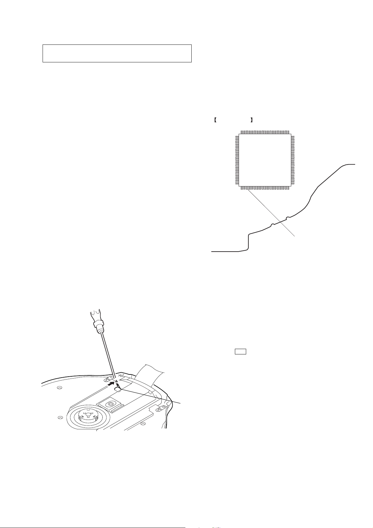
D-NE10
SERVICE MODE
The following confirmation can be performed when the Service
Mode is set.
1. How to set the Service Mode.
To set the Service Mode, the following method is available.
1) Confirm the set is not powered on.
2) Confirm the following settings.
OPEN/CLOSE detect switch (S812) ........ OFF
Solder Land (SL812) ................................ OPEN
[HOLD] switch (S802)............................... OFF
3) Short the solder land SL805 (TEST) on the MAIN board.
4) Turn on the main power.
MAIN BOARD (SIDE B)
SL805 (TEST)
2. Operation when the Service Mode is set.
When the Service Mode becomes active, following messages are
displayed onthe remote control LCD.
Microcomputer
version display
VP094P:
or
VP098C:
1) Turn off the power.
2) Open the solder land SL805 (TEST) on the MAIN board.
Note : The solder should be removed clean.
SL812 (OPEN)
S812
4

SECTION 2
1
GENERAL
Locating the controls
CD player (rear)
For details, see the pages in parentheses.
2
3
4
5
6
7
*1/–
1 VOL (volume) +
1
2 u*
3 x (stop)/CHG (charge) button (15, 29)
4 ./> (AMS*
5
6 Terminals for the charging stand/external
7 OPEN switch (14, 28)
8 HOLD switch (23)
(play/pause) button (14, 15)
(group) +/– buttons (15, 20)
battery case (14, 29, 30)
Squeeze the switch from both sides.
Slide the switch in the direction of the
arrow to disable the buttons on the CD
player.
buttons (15)
2
/search) buttons (15)
This section is extracted
from instruction manual.
8
9
q;
9 OPERATION lamp (front)
Color of the lamp changes according to
the type of music source being played.
Red: Audio CD, Green: ATRAC3plus/
ATRAC3 file, Orange: MP3 file
For some time after the CD is inserted,
the lamp lights up in red, orange and
green in turn.
This lamp also functions as the HOLD
lamp and the CHG (charge) lamp.
q; i (headphones)/LINE OUT (OPTICAL)
jack (14, 26)
Switch the function of the jack, using the
menu.
(14, 23, 24, 29)
D-NE10
Remote control
For details, see the pages in parentheses.
1
2
3
4
5
1 VOL (volume) +/– control (15, 21, 23)
Turn to adjust the volume.
2 x (stop) button (15, 22, 23, 32)
3 Jog lever (. u/ENT >) (15, 18
- 26)
u (play/pause)/ENT (enter):
Press during stop to start play, and press
during play to pause play. When
selecting menu items, press to enter the
selection.
Flick toward . or >: AMS, rewind,
fast forward
4 Display (13, 16)
5
(group) +/– buttons (15, 20)
*1 The button has a tactile dot.
*2 Automatic Music Sensor
6
7
8
9
q;
6 Clip (13)
7 HOLD switch (23)
Slide the switch in the direction of the
arrow (a yellow mark appears) to disable
the buttons on the remote control.
8 DISPLAY button (22 - 26, 32)
9 P MODE/
q; SOUND button (21)
Note
Use only the supplied remote control. You cannot
operate this CD player with the remote control
supplied with other CD players.
button (17 - 20)
5

D-NE10
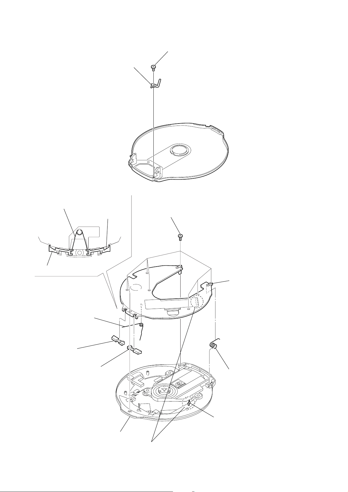
DISASSEMBLY
Note : Disassemble the unit in the order as shown below.
UPPER LID (SUB) ASSY
MAIN BOARD,
CD MECHANISM DECK
(CDM-3325ER2)
TURN TABLE MOTOR ASSY (M901),
SLED MOTOR ASSY (M902),
OPTICAL PICK-UP (DAX-25E)
SECTION 3
SET
LIGHT GUIDE LENS
CABINET (INNER)
6

Note : Follow the disassembly procedure in the numerical order given.
3-1. UPPER LID (SUB) ASSY
1
two tapping screws
3
bracket (hinge L)
2
bracket (hinge R)
D-NE10
4
Close the cover until the tip of the cover of the
top cover (SUB) assembly is left open by 5 mm,
then slide the top cover (SUB) assembly in the
direction of the arrow.
6
7
upper lid (SUB) assy
5
7
D-NE10
3-2. LIGHT GUIDE LENS
3-3. CABINET (INNER)
spring (lock claw)
2
light guide lens
lock claw (L)
1
1
eight screws
screw
lock claw (R)
4
spring (lock claw)
2
lock claw (L)
3
lock claw (R)
cabinet (lower) assy
5
cabinet (inner)
6
spring (upper lid)
battery terminal board (+)
Note: It is recommended to visually check that the battery terminal board (+) is
installed in the specified position after assembling the cabinet (INNER)
because, in some cases, the battery terminal board (+) cannot be housed
when assembling the cabinet (INNER).
8
3-4. MAIN BOARD, CD MECHANISM DECK (CDM-3325ER2)
1
spacer (disc)
spacer (disc)
3
connector (4P)
2
connector (2P)
6
CD mechanism deck
(CDM-3325ER2)
5
three insulators
4
flexible board
D-NE10
(CN501)
8
battery terminal board (-)
7
Remove two solders
of the MAIN board.
qd
control button
qf
knob (hold)
qs
MAIN board
0
battery terminal board (+)
qa
static electricity incorrect operation
prevention earth
9
Remove two solders
of the MAIN board.
9
D-NE10
3-5. TURN TABLE MOTOR ASSY (M901), SLED MOTOR ASSY (M902), OPTICAL PICK-UP (DAX-25E)
1
three screws
5
three screws
(B 1.7
×
(B 1.7
4)
×
4)
3
sled motor assy
(M902)
2
gear cover
4
optical pick-up
(DAX-25E)
6
turn table motor assy
(M901)
chassis
10

e
RF level
0.45 to 0.65 Vp-p
SECTION 4
ELECTRICAL CHECKING
D-NE10
The CD section adjustments are done automatically in this set.
In case of operation check, confirm that RF level.
Precautions for Check
1. Perform check in the order given.
2. Use YEDS-18 disc (Part No.: 3-702-101-01) unless otherwise
indicated.
3. Power supply voltage requirement : DC3 V in terminals for the
charging stand.(J401,402)
VOLUME button : Minimum
HOLD switch : OFF
AVLS function setting : OFF
G-PROTECTION function setting : 1
Checking Location:
– MAIN board (Side A) –
RF Level Check
Condition:
• Hold the set in horizontal state.
Connection:
Oscilloscop
(AC range)
MAIN board
2 k
TP649 (RF)
TP701 (AGND)
Ω
+
–
Procedure:
1. Connect the oscilloscope to the test points TP649 (RF) and
TP701 (AGND) on the MAIN board.
2. Set a disc. (YEDS-18)
3. Press the u button.
4. Check the oscilloscope waveform is as shown below.
A good eye pattern means that the diamond shape (◊) in the
center of the waveform can be clearly distinguished.
RF Signal reference Waveform (Eye Pattern)
VOLT/DIV : 100 mV (With the 10:1 probe in use)
TIME/DIV : 500 ns
TP649
TP701(AGND)
1
15
To watch the eye pattern, set the oscilloscope to AC range and
increase the vertical sensitivity of the oscilloscope for easy watching.
5. Stop revolving of the disc motor by pressing the x button.
11

D-NE10
SECTION 5
DIAGRAMS
NOTE FOR PRINTED WIRING BOARDS AND SCHEMATIC DIAGRAMS
Note on Printed Wiring Board
• X : parts extracted from the component side.
• Y : parts extracted from the conductor side.
• : Pattern from the side which enables seeing.
(The other layers' patterns are not indicated.)
Caution:
Pattern face side: Par ts on the pattern face side seen from
(Side B) the pattern face are indicated.
Parts face side: Parts on the par ts face side seen from
(Side A) the parts face are indicated.
• MAIN board is multi-layer printed board. However, the patterns of intermediate-layer have not been included in the diagram.
Note on Schematic Diagram:
• All capacitors are in µF unless otherwise noted. pF: µµF 50 WV or
less are not indicated except for electrolytics and tantalums.
• All resistors are in Ω and 1/
•%: indicates tolerance.
• C : panel designation.
Note:
The components identified by
mark 0 or dotted line with mark
0 are critical for safety.
Replace only with part number
specified.
• A : B+ Line.
•Total current is measured with CD installed.
•Power voltage is dc 4.5 V and fed with regulated dc power supply
from DC IN jack (J401).
•Voltages and waveforms are dc with respect to ground in playback
mode.
no mark : CD PLAY
* : Impossible to measure
•Voltages are taken with a VOM (Input impedance 10 MΩ).
Voltage var iations may be noted due to normal production tolerances.
•Waveforms are taken with a oscilloscope.
Voltage var iations may be noted due to normal production tolerances.
• Circled numbers refer to waveforms.
• Signal path.
J : CD PLAY (ANALOG OUT)
c : CD PLAY (OPTICAL OUT)
4
W or less unless otherwise specified.
Note:
Les composants identifiés par
une marque 0 sont critiques
pour la sécurité.
Ne les remplacer que par une
pièce portant le numéro spécifié.
• WA VEFORMS
1
IC601 if RFAC
100mV/DIV, 400ns/DIV
540 mVp-p
5
IC702 e; XTAL
1V/DIV, 20ns/DIV
2.8 Vp-p
44ns
2
IC601 rk XTAO
1V/DIV, 20ns/DIV
2.7 Vp-p
59ns
✩When IC802 is damaged, replace the MAIN board.
3
IC801 wk XIN
1V/DIV, 40ns/DIV
2.1 Vp-p
118ns
4
IC401 5 SYNC
1V/DIV, 2us/DIV
5.7us
2.2 Vp-p
12

5-1. BLOCK DIAGRAM – MAIN SECTION -1 –
DETECTOR
PD
A
LD
B
• SIGNAL PATH
A
B
RF
E
F
VCC
OPTICAL PICK-UP BLOCK
DAX-25E
LASER DIODE
PD
(FOCUS)
2-AXIS
DEVICE
(TRACKING)
M902
SPINDLE
MOTOR
V
U
W
: CD PLAY (ANALOG OUT)
: CD PLAY (OPTICAL OUT)
A
B
RF
E
F
VCC3
OPGSW
OPSTB
LD
M901
M
SLED
MOTOR
U1
25
V1
24
W1
23
COM
26
U
30
V
32
W
34
+
+
+
MOTOR
DRIVER
IC401 (1/3)
FOCUS/TRACKING COIL DRIVER
SLED MOTOR DRIVER
FO3
38
RO3
36
FO1
46
44
42
40
CONTROLLER,
RO1
H BRIDGE DRIVER
FO2
RO2
IC401 (2/3)
SPINDLE MOTOR DRIVER
CONTROL
CIRCUIT
FI3
RI3
FI1
RI1
FI2
RI2
APWM
XBRK
D-NE10
IC601
RF AMP,
DIGITAL SIGNAL PROCESSOR,
DIGITAL SERVO PROCESSOR,
D-RAM CONTROLLER
A
92
B
91
RFDC
88
RFAC
84
E
89
F
90
SFDR
52
53
48
49
50
51
IC403 (1/2)
SWITCH
12
7
27
21
FG
22
100
99
96
95
98
97
104
103
102
10
58
SRDR
FFDR
FRDR
TFDR
TRDR
C176
MDP
MDS
FG_I
MDP_SW
HG_GUP_O
12
13
SCOR
27
SCOR_I
HG_XSTB_O
WFCK
MDS
XTAO
XTAI
RFAC
XSOE
SENS
R4M
XLAT
CLOK
SCOR
SDTO
RFDC
SFDR
SRDR
FFDR
FRDR
TFDR
TRDR
SIGNAL
PROCESSOR
BLOCK
MDP
E
F
B
A
SDTO
SENS
858887838486
MSDTO0_O
IC801 (1/3)
SYSTEM CONTROLLER
MEMORY
CONTROLLER,
BASS BOOST
BLOCK
SERVO
BLOCK
R8M
CLOK
MSCK_O
MSDTI0_I
XSOE
XLAT
32 65
2422
232021
28
XIN
XSOE_O
XLAT0_O
28
XRST
4
XRST_O
DIGITAL
OUT
FOK
GFS
LPF
GFS
69
53
GFS_I
AOUT1
AOUT2
PCMD_O
FOK
52
FOKI
AT3_MP3_V_O
WAKEUP_K_O
SDOUT_O
SDCLK_O
SDXLAT_O
EEP_CS_O
DOUT
62
D0-D3
4, 3, 6, 5
A0-A10
116 – 113, 17 – 15, 13 – 11, 117
XRAS
1
XWE
2
XCAS
9
XTAI
47
XTAO
48
51
56
108
106
LRCK_O
110
BCK_O
109
PCMD_I
107
LRCK_I
111
BCK_I
XRDE
18
X701
22MHz
60
66
REQ_I
11
SDIN_I
20
19
18
17
67
D0 – D3A0 – A10
2, 3, 24, 25
9 – 12, 15 – 19, 21, 8
5
XRAS
4
XWE
23
XCAS
X601
16.9344MHz
4
PCMD
1
LRCK
2
BCK
15
PI0
14
PI2
13
PI3
12
PF4
29
EXTAL
30
XTAL
IC602
D-RAM
IC702
MP3 DECODER
PF0
NRST
33
34
37
DOUT
AOUTL,
AOUTR
PF3
40
SYNC
PC1
C
D
PC0
PC2
PC3
41
38
42
4
3
2
1
IC802
EEPROM
DO
DI
XSK
XCS
E
MSCK
F
MSDTO
G
1313

D-NE10
– MAIN SECTION -2 –
DOUT
C
AOUTL, AOUTR
D
Q301
MUTING
CONTROL
SWITCH
AOUTL
AOUTR
IC301
HEADPHONE AMP
5
L-IN
3
R-IN
1
MUTE
2
MSW
16
BEEP
LOUT
VCC1
Q304, 804
VCC3
12
14ROUT
RMKEY
TSB
VCPU
Q302, 303
8
B+ SWITCH
VCC2
J301
LINE OUT
(OPTICAL)
(REMOTE)
7
AMUTE_O
XLED2_O
76
Q803
LED DRIVER
D804
OPR
XLED1_O
75
65
HP_LIN_SEL_O
LID-SW_I
37
S812
(OPEN/CLOSE)
6
BEEP_O
HOLD_I
40
S802
> HOLD
IC801 (2/3)
SYSTEM CONTROLLER
ON
OFF
97
S811
x
77
AD-KEY2
HP_PWRSW
AD-KEY1
96
S803 - 809
FUNCTION
KEY
70
9
OPTOUT_I
OPTPWRCTL_O
Q801(2/2)
SWITCH
8
31
TSB
LINEOUT_I
JOGKEY_I/FAVKEY_I
36
Q801(1/2)
SWITCH
AD-RMKEY
99
• SIGNAL PATH
: CD PLAY (ANALOG OUT)
: CD PLAY (OPTICAL OUT)
1414

– POWER SECTION –
PD
A
D-NE10
LD
B
SYNC
E
MSDTO
G
MSCK
F
PWRLAT_O
XWAKE_O
XRESET_I
IC801 (3/3)
SYSTEM CONTROLLER
VDSEL
90
32
8
57
VCPU 1.9V
IC702 AVD
VCC2
IC701
Q405
SWITCH
VCC1 1.9V
VCC4
VCC3
VIN
VIN/VD
IC601
IC602
RV401
VCPU
VIN
Q404
SWITCH
VD
D403
IC403 (2/2)
SWITCH
3
IC401 (3/3)
POWER CONTROL
PA PC
97
VLGO4
78
INM4
100
RF4
99
RF41
96
SYNC
5
DATA
8
CLOCK
7
LATCH
9
WAKE
6
RSTB
10
VDRAM
59
VCC1
61
INP2
70
VLGO2
86
VCPU
60
VCC4IN
77
VCC4
76
VCC3
91
VCC2
90
INP3
92
L2L
85
VDSW20
20
VDSW19
19
INP7
15
65
VLG07
14
CHGSW
RF1
VINDET
RS1
VIN
RF41
RF4
INM4
APCREF
PAPC
INP2
INP3
VCC1
VCC2
VCC3
VCC4
VCC4IN
VCPU
L2L
WAKE
LATCH
DATA
CLOCK
LINEAR
CONSTANT CURRENT,
CONSTANT VOLTAGE
CHARGING BATTERY
CHARGE CIRCUIT
SWITCHING
POWER
CIRCUIT
SWITCHING
POWER
CIRCUIT
INTERFACE
OR OSC
SAW
GEN.
CLK
CHARGING BATTERY
VOLTAGE DETECTOR
CIRCUIT
PRE-DRIVER
VG
POWER
CIRCUIT
VLGO4
VLGO2
VG
L5
BATM1
CHGMNT
DCIN
BATM1
RF1
DCIN
RS1
CHGSW
VIN
VINDET
L410
CHARGE
D402
VIN
D401
RECHARGEABLE
BATTERY
NH-14WM
1PC. 1.2V
J401
(EXT BATT)
J402
(CHARGING STAND)
VG
3
L5
2
74
58
65
55
66
82
98
Q402
CHARGE
SWITCH
D404
Q401
B+
SWITCH
AD-CHGMNT
AD-DCINMNT
AD-BATMNT
AD-CHGSTMNT
EXTBAT_I
UPCKB7
VIN
Q403
SWITCH
93
95
92
94
38
13
11
72
UPCK7
CHGMNT
Q406
EXTERNAL BATTERY
DETECT
1515

D-NE10
5-2. PRINTED WIRING BOARDS – MAIN BOARD (SIDE A) –
12
MAIN BOARD
(SIDE A)
A
OPR
B
C
• : Uses unleaded solder.
3456789
J401
(EXT BATT)
RECHARGEABLE
BATTERY
NH-14WM
1PCS.1.2V
D
E
F
G
OPTICAL
PICK-UP
BLOCK
DAX-25E
1-860-218-
J402
(CHARGING STAND)
E
E
15
1
14
12
M901
M
SLED
+
MOTOR
V
W
U
M902
3 PHASE
SPINDLE
MOTOR
11
(11)
MAIN BOARD
(SIDE A)
• Semiconductor
Location
J301
LINE OUT
(OPTICAL)
(REMOTE)
Ref.No. Location
D101 F-5
D202 F-5
D303 F-7
D804 B-1
Q304 F-6
Q804 E-6
1616

D-NE10
5-3. PRINTED WIRING BOARDS – MAIN BOARD (SIDE B) –
12
MAIN BOARD
A
(SIDE B)
.
E
B
C
IC401
• : Uses unleaded solder.
✩When IC802 is damaged, replace the MAIN board.
3456789
>
> HOLD
OFF
ON
IC403
x
IC701
54
13
u
IC702
VOL
IC802
D
E
F
G
MAIN BOARD
(SIDE B)
• Semiconductor
IC801
E
E
E
E
E
IC602
IC601
E
1-860-218-
S812
(OPEN/CLOSE)
IC301
PROGRAMMER
11
(11)
Location
Ref.No. Location
D302 F-4
D304 G-5
D305 F-4
D306 F-4
D308 G-5
D401 E-2
D402 E-2
D403 C-2
D404 D-2
D405 B-3
D406 C-4
D805 E-7
IC301 E-3
IC401 C-2
IC403 C-4
IC601 E-5
IC602 D-4
IC701 A-4
IC702 B-5
IC801 D-7
IC802 B-7
Q301 E-4
Q302 E-3
Q303 E-2
Q401 E-2
Q402 E-2
Q403 D-3
Q404 D-3
Q405 D-3
Q406 B-3
Q801 E-6
Q803 B-3
1717

D-NE10
5-4. SCHEMATIC DIAGRAMS – MAIN BOARD (1/4) –
MAIN BOARD (1/4)
OPTICAL
PICK-UP
BLOCK
DAX-25E
M902
3 PHASE
SPINDLE MOTOR
U
M901
SLED
MOTOR
W
V
15P
15
14
13
12
11
10
9
8
7
6
5
4
3
2
1
4P
4
3
2
1
2P
2
1
• See page 12 for Waveform. • See page 23 for IC Block Diagrams.
0UH
2.6
0
0
1.9
1.9
1.3
1.3
1.3
0UH
X601
16.934MHz
1.3
0.9
0.9
2.6
2
0UH
1.9
1.9
IC601
1.9
1
1
0.9
0.9
0.9
1
0.9
0.9
0.7
1.9
0.9
1.9
0.9
1.1
1.1
1.1
1
1.2
1.2
000
0.3
0.1
0.1
0.1
RF AMP
DIGITAL SIGNAL PROCESSOR
DIGITAL SERVO PROCESSOR
D-RAM CONTROLLER
IC601
CXD3039AR
1.9
0.411.901.9
000
0
11111
1.9
<21>
<22>
<23>
<24>
<25>
<26>
<27>
<28>
1.9
1.9
1
0
0
1.9
0.1
0.1
0
1.7
1.9
1.7
1.9
1.9
1.9
1.9
1
1
0.9
0.9
0.9
0.9
1.6
1
1
1
1
1.5
1.3
IC602
IC602
MSM51X17400F-10TFSR1
1.9
1
1
1.5
1.3
D-RAM
1
1
1
1
1
1.9
1
1
1.6
0.9
0.9
0.9
0.9
1
1
<29>
<30>
<31>
<32>
B
MAIN
BOARD
(3/4)
<1>
<3>
<4>
<5>
<6>
<7>
<8>
<9>
<10>
<11>
<12>
A
MAIN
BOARD
(2/4)
<13>
<33>
<34>
<36>
C
MAIN
BOARD
(4/4)
No mark : PLAY (servo on)
<14>
<15>
<16>
<17>
<18>
<19>
<20>
1818

D-NE10
5-5. SCHEMATIC DIAGRAMS – MAIN BOARD (2/4) –
MAIN BOARD (2/4)
<1>
<3>
• See page 12 for Waveform.
<4>
<5>
<6>
<7>
<8>
<9>
MAIN
BOARD
A
(1/4)
<10>
<11>
<12>
0.1
0.3
0.1
0.2
1.2
0.1
0.1
1.2
0
0
1.3
0
0.4
1.2
0.4
0.4
<13>
IC403
SN74LVC2G66DCUR
*
1.2
1.9
SWITCH
1.2
0.4
0.3
1.2
2.7
0
0.7
0.7
IC403
<14>
<15>
<16>
<17>
<18>
<19>
<20>
<37>
<38>
<39>
<40>
J401
(EXT BATT)
• TOTAL CURRENT
PLAY : 110mA
STOP : 53mA
FF : 100mA
FR : 150mA
1P
B+
SWITCH
0.3
0
0
0.8
0
1.2
0.1
0.2
1.9
0.1
0.1
0.7
0
2SD2652T106
0
CHARGE
0
SWITCH
1.9
1.4
2SA1602TP-1EF
1.9
1.9
1.9
3.3
0.1
0.2
0
0.7
0.7
0.7
0.7
0
0
1.5
1.9
1.9
1.1
1.2
1.2
IC401
SPINDLE MOTOR DRIVER
IC401
TB2166FG
1.2
1.9
1.2
1.2
2.7
4
2.4
0.6
0.6
0.2
0.1
0.2
0.2
0.9
0.5
0.4
0.4
0.4
1
1.9
0
7
0.1
0.4
0.6
0.6
1.3
5.9
1.9
0.3
1.9
1.9
1.9
1.9
0
0.9
7
1.2
1.2
0.2
1.2
0.3
1.9
1.3
1.2
5.9
SWITCH
7
1.2
MAIN
BOARD
D
(4/4)
0
1.2
SWITCH
1.3
0
1.2
0
SWITCH
0
RECHARGEABLE
BATTERY
NH-14WM
1PCS.1.2V
J402
(CHARGING STAND)
1P
EXTERNAL BATTERY
DETECT
<41>
<42>
<43>
No mark : PLAY (servo on)
* : Impossible to measure
1919

D-NE10
5-6. SCHEMATIC DIAGRAMS – MAIN BOARD (3/4) –
MAIN BOARD (3/4)
<21>
<22>
<23>
<24>
<25>
<26>
<27>
<28>
• See page 12 for Waveform. • See page 23 for IC Block Diagrams.
0
MUTING CONTROL
SWITCH
BCR119W-GEG-E6327
1.6
Q303
10V
IC301
IC301 AN17020B-E1
1.3
0.3
1.3
1.3
1.2
2.7
2.7
2.4
SWITCH
2.4
0
0
1.3
0.6
0.6
1.3
10V
1.2
0.6
10V
J301
LINE OUT
(OPTICAL)
(REMOTE)
B
MAIN
BOARD
(1/4)
<29>
<30>
<31>
<32>
<33>
<34>
IC701
2.7
2.7
XN0NE9200LS0
SWITCH
IC701
1.5
2.7
2.7
1.4
1.4
0
1.9
1.9
1.9
0
1.9
1.9
1.9
1.9
1.9
1.5
0
0
1.9
2.7
0
5
1.9
IC702
MP3 DECODER
IC702
CXR710160-207R
1.5
1.9
0
0
0
0
1.9
1.9
1.9
1.5
1.5
0
1.9
0
0
1.9
2.7
2.7
2.1
1.9
B+
SWITCH
B+
SWITCH
0
Q303
BCR119W-GEG-E6327
S812
(OPEN/CLOSE)
<44>
<45>
<46>
<47>
<48>
<49>
<50>
E
MAIN
BOARD
(4/4)
OFF
S802
> HOLD
ON
No mark : PLAY (servo on)
<51>
<52>
<53>
<54>
<55>
<56>
<57>
<58>
<59>
2020

D-NE10
5-7. SCHEMATIC DIAGRAMS – MAIN BOARD (4/4) –
MAIN BOARD (4/4)
<44>
<45>
MAIN
BOARD
(1/4)
MAIN
BOARD
(2/4)
C
D
<36>
<37>
<38>
0
1.9
<39>
<40>
• See page 12 for Waveform.
SWITCH
*
<46>
<47>
0
1.9
0
1.9
0
0
0
1.9
1.9
1.6
0
1.9
1.8
1.9
1.9
1.2
0
1.9
0
1.9
1.9
1.9
0
1.9
<48>
2.4
SWITCH
0
1.9
✩When IC802 is damaged, replace the MAIN board.
MAIN
BOARD
E
(3/4)
<59>
<49>
0
1.9
1.9
1.901.9
IC801
SYSTEM CONTROLLER
TMP91CY28FG-2772-01
1.9
IC801
<50>
1.901.9
1.9
3
<51>
<52>
<53>
1.9
1.9
0
1.9
0
1.7
0
0
TP806
1
1.9
1.9
1
<54>
<55>
<56>
1.9
1.9
1.9
1.9
<57>
IC802
EEPROM
<58>
10P
PROGRAMMER
1.9
u
<41>
<42>
<43>
0
0100000
1.9
1.9
1.9
0.2
1.9
1.9
1.9
1.9
1.9
1.9
0.2
1.3
0
0.1
SWITCH
*
0.4
>
.
+
–
+
VOL
–
x
No mark : PLAY (servo on)
* : Impossible to measure
2121

D-NE10
• IC Block Diagrams
IC301 AN17020B-E1 IC702 CXR170160-207R
BEEP
GA-R
ROUT
GND
LOUT
GA-L
VCC2
14 1316 15 12 11 10 9
BEEP
+- +-
RF2
VCC2
NTRST
TDO
TMS
VDIO3
TDI
TCK
64 63 62 61 60 59 58 57 56 55 5354 52 51 50 49
TEST0
DVSS1
DVDD3
TEST1
TEST2
TRST(TEST4)
TEST3
XOUT(TEST5)
TACK(TEST6)
VDIO2
MUTE
MSW
MUTE
HP/Line
SW
3 4 5 6 7 821
R-IN
PE3/RxD148
PE2/TxD147
RF1
L-IN
GND
HVCC1
VREF
VCC1
LRCK
BCK
VDIOCD0
PCMD
DVDD4
TAPTDO
SCANEN
DCDD0
DVSS0
DVIO0
VDIOCD1
PF4/XRDE
P13/BCKO
P12/LRCKO
P10/PCMDO
EVA
DAC
1
2
3
4
5
6
7
INTERFACE
CD-ROM
INTERFACE
8BIT TIMER (CH7)
8BIT TIMER (CH6)
8BIT TIMER (CH5)
8BIT TIMER (CH4)
UART (CH1)
8BIT TIME
8BIT TIMER/COUNTER (CH2)
8BIT TIMER (CH1)
8BIT TIMER/COUNTER (CH0)
UART (CH0)
SERIAL INTERFACE
(CH0)
RAM
8
9
10
11
12
13
14
15
EEPROM SERIAL
INTERFACE
MAGIC GATE
CORE
INTERRUPT CONTROLLER
282
16
DMAC (CH3)
DMAC (CH2)
WATCHDOG TIMER
PRESCALLER/
TIME BASETIMER
DMAC (CH1)
DMAC (CH0)
CLOCK GENERATOR/
SYSTEM CONTROLLER
PE1/RxD046
PE0/TxD045
44
DVDD2
43
DVSS2
42
PC3/SCS0
41
PC2/SI0
40
PC1/SO0
39
VDIOCD2
38
PC0/SCK0
37
PF3/T3
36
PF2/EC2/INT4
35
PF1/T1
34
PF0/EC0/INT3
33
NRST
RAM
17 18 19 20 21 22 23 24 25 26
KDI
KCLK
KCS
VDIO1
KDO
KRB
DVDD1
DVSS3
AVDPLL
AVSPLL
160K BYTES
RAM
512K BYTES
27 28 29
AVDMO
AVSSOSC
VIRTUAL ENGINE
CORE
ARM77TDMI
CPU CORE
30
XTAL
EXTAL
31 32
XIN
OSCSEL
2222
HUFFMAN HW

5-8. IC PIN FUNCTION DESCRIPTIONS
• IC601 CXD3039AR
(RF AMP, DIGITAL SIGNAL PROCESSOR, DIGITAL SERVO PROCESSOR, D-RAM CONTROLLER)
Pin No. Pin Name I/O Description
1XRAS
2
3 to 6
7DCLK O
8DCKE O
9XCAS O
10
11 to 13 A9 to A7 O
14 DVSS —
15 to 17 A6 to A4 O
18 XRDE I
19
20 CLOCK
21 SDTO
22 SENS
23
24
25 SYSM
26
27
28 XRST I
29 PWMI
30 XQOK
31 XWRE I
32 R8M O System clock output to the system controller
33 VSS0 —
34 SQCK I SQSO readout clock input terminal Not used
35 SCLK I SENS serial data read clock input terminal Not used
36
37
38
39
40 EXCK O SQSO readout clock output terminal Not used
41 XTSL I
42 HVSS —
43 HPL O PDM signal output for L-ch headphone to the headphone amplifier Not used
44 HPR O PDM signal output for R-ch headphone to the headphone amplifier Not used
45
46
47 XTAI I
48 XTAO O
49 XVSS —
50
51 AOUT1 O L-ch analog audio signal output
52 VREFL O
XWE
D1, D0, D3, D2
WFCK O WFCK signal output terminal Not used
VDD0 — Power supply terminal (digital system)
XLAT I Serial data latch pulse signal input from the system controller
XSOE I Serial data output enable signal input from the system controller
WDCK O GRSCOR signal output to the system controller Not used
SCOR O Subcode sync (S0+S1) detection signal output to the system controller
SQSO O CD text data output terminal Not used
XEMP O D-RAM read prohibition signal output terminal Not used
XWIH O D-RAM write prohibition signal output terminal Not used
SBSO O Subcode P to W serial data output terminal Not used
HPVDD — Power supply terminal (for headphone)
XVDD — Power supply terminal (for master clock)
AVDD1 — Power supply terminal (analog system)
O Row address strobe signal output to the D-RAM
O Data input enable signal output to the D-RAM
I/O
Two-way data bus with the D-RAM
Not used
Not used
Column address strobe signal output to the D-RAM
Address signal output to the D-RAM
Ground terminal (for D-RAM interface)
Address signal output to the D-RAM
D-RAM read enable signal input terminal
I Serial data transfer clock input from the system controller
I Serial data input from the system controller
O Serial data output to the system controller
I Analog muting on/off control signal input “H”: muting on Not used
Reset signal input from the system controller “L”: reset
I Spindle motor external control signal input terminal Not used
I Subcode Q OK signal input terminal Not used
D-RAM write enable signal input terminal Not used
Ground terminal (digital system)
Input terminal for the system clock frequency setting
“L”: 16.9344 MHz, “H”: 33.8688MHz (fixed at “L” in this set)
Ground terminal (for headphone)
System clock input terminal (16.9344 MHz)
System clock output terminal (16.9344 MHz)
Ground terminal (for master clock)
L-ch reference voltage output terminal
D-NE10
23

D-NE10
Pin No. Pin Name I/O Description
53, 54 AVSS1, AVSS2 —
55 VREFR O
56 AOUT2 O R-ch analog audio signal output
57
58 TES1 I Input terminal for the test (normally: fixed at “L”)
59 TEST I Input terminal for the test (normally: fixed at “L”)
60 VSS1 —
61 LRMU
62 DOUT O Digital audio signal output
63 ATSK I/O Input/output terminal for anti-shock Not used
64 DFCT I/O Defect signal input/output terminal Not used
65 FOK O
66 MIRR I/O Defect signal input/output terminal Not used
67 COUT I/O
68
69
70
71
72
73 PCO O
74 FILI I
75 FILO O
76 CLTV I
77 VCTL I
78 VPCO O
79 AVSS3 —
80 ASYO O
81 ASYI I
82 BIAS I
83
84 RFAC I
85
86 IGEN I
87 AVSS0 —
88 RFDC I
89 E I
90 F I
91 B I
92 A I
93 VC I
94 VSS3 —
95 FRDR O
96 FFDR O
97 TRDR O
98 TFDR O
99 SRDR O
AVDD2 — Power supply terminal (analog system)
C2PO O C2PO signal output terminal Not used
GFS O GFS signal output terminal
XUGF O XUGF signal output terminal Not used
XPCK O XPCK signal output terminal Not used
VDD1 — Power supply terminal (digital system)
AVDD3 — Power supply terminal (analog system)
AVDD0 — Power supply terminal (analog system)
Ground terminal (analog system)
R-ch reference voltage output terminal
Ground terminal (digital system)
Muting on/off control signal output to the audio line and the headphone amplifier
O
“H”: muting on Not used
Focus OK signal output to the system controller “L”: NG, “H”: OK
Numbers of track counted signal input/output terminal Not used
Charge pump output for master PLL
Filter input for master PLL
Filter output for master PLL
VCO1 control voltage input terminal for multiplier
VCO2 control voltage input terminal for broad-band EFM PLL
Charge pump output terminal for broad-band EFM PLL
Ground terminal (analog system)
EFM full-swing output terminal
Asymmetry comparator voltage input terminal
Asymmetry circuit constant current input terminal
EFM signal input from the optical pick-up
Stabilized current input for operational amplifiers
Ground terminal (analog system)
RF signal input from the optical pick-up
E signal input from the optical pick-up
F signal input from the optical pick-up
B signal input from the optical pick-up
A signal input from the optical pick-up
Middle point voltage input terminal Not used
Ground terminal (digital system)
Focus servo drive signal (–) output to the IC401
Focus servo drive signal (+) output to the IC401
Tracking servo drive signal (–) output to the IC401
Tracking servo drive signal (+) output to the IC401
Sled servo drive signal (–) output to the IC401
24

Pin No. Pin Name I/O Description
0
100 SFDR O
101 SSTP I
102 MDS O
103 MDP O
104 C176 O
105
106 LRCK O
107 LRCKI I
108 PCMD O
109 PCMDI I
110 BCKO O
111 BCKI I
112
113 to 117 A3 to A0, A10 O
118 to 12
VDD2 — Power supply terminal (digital system)
DVDD — Power supply terminal (for D-RAM interface)
A11 to A13 O
Sled servo drive signal (+) output to the
Disc inner position detection signal input terminal Not used
Spindle motor drive signal output to the spindle motor driver
Spindle motor servo control signal output to the spindle motor driver
176.4 kHz clock output to the power control and spindle motor driver
L/R sampling clock (44.1 kHz) output terminal
L/R sampling clock (44.1 kHz) input terminal
Serial data output terminal
Serial data input terminal
Bit clock (2.8224 MHz) output terminal
Bit clock (2.8224 MHz) input terminal
Address signal output to the D-RAM
Address signal output terminal to the D-RAM Not used
IC401
D-NE10
25

D-NE10
• IC801 TMP91CY28FG-2772-01 (SYSTEM CONTROLLER)
Pin No.
1
2
3
4
5
6
7
8
9
10
11
12
13
14
15
16
17
18
19
20
21
22
23
24
25
26
27
28
29
30
31
32
33
34
35
36
37
38
39
40
41
42
43
44 to 51
52
53
54
55
56
57
Pin Name
GND
GND
VCPU
XRST_O
PWM_O
BEEP_O
AMUTE_O
LINEOUT_I
OPTOUT_I
FG_I
REQ_I
HG-XSTB_O
HG-GUP_O
RE1_I
RE2_I
LCD_REQ_O
SDXLAT_O
SDCLK_O
SDOUT_O
SDIN_I
DTS_SDTO
DTS_SDTI
DTS_SCK
AM0_I
VCPU
XOUT
GND
XIN
AM1_I
XRESET_I
TSB
XWAKE_O
EMU0_O
EMU1_O
ACKCD_I
JOGKEY_I/FAVKEY_I
LID-SW_I
EXTBAT_I
HP_TYPE_I
HOLD_I
X_PEQ_EN_I
TEST_I
NC
AD0 to AD7
FOK_I
GFS_I
TUPWRON_O
CDON_O
AUD_SEL_O
VDSEL
I/O
—
Reference voltage terminal (A/D converter)
—
Ground terminal (A/D converter)
—
Power supply terminal (A/D converter)
O
Reset signal output to the DSP (IC601)
O
Not used (open)
O
BEEP signal output
O
Muting signal output to the headphone amplifier (IC301)
I
Line plug in detection signal input (“H” : line plug in)
I
Optical plug in detection signal input (“H” : optical plug in)
I
FG (3 phase drive) signal input from the power control (IC401)
I
Request signal input from the MP3 decoder (IC702)
O
HG sleep mode signal output to the optical-pickup
O
HG gain up signal output to the optical-pickup
I
Not used (open)
I
Not used (open)
O
Not used (open)
O
Serial data latch signal output to the MP3 decoder (IC702)
O
Clock output to the MP3 decoder (IC702)
O
Serial data output to the MP3 decoder (IC702)
I
Serial data input from the MP3 decoder (IC702)
O
Not used
I
Not used
O
Not used
I
Not used (fixed at “H”)
—
Power supply terminal
O
Clock output (not used)
—
Ground terminal
I
Clock input
I
Not used (fixed at “H”)
I
Reset signal input (“L” : reset)
I/O
Data input/output from/to the remote control
O
Wake signal output to the power control (IC401) (“L” : running)
O
Not used (open)
O
Not used (open)
I
Not used (fixed at “L”)
I
Key signal input from the jog key or the remote control key
I
Lid open/close detection signal input (“H” : lid open)
I
External battery in detection signal input (“H” : external battery in)
I
Not used
I
HOLD switch detection signal input (“H” : HOLD on)
I
Not used
I
Test mode setting terminal (“L” : test mode)
—
Not used (open)
I/O
Not used (open)
I
FOK signal input from the DSP (IC601)
I
GFS signal input from the DSP (IC601)
O
Not used (open)
O
Not used (open)
O
Not used (open)
O
Power supply voltage selection signal output
Description
26

D-NE10
Pin No.
58
59
60
61
62
63
64
65
66
67
68
69
70
71
72
73
74
75
76
77
78
79
80
81
82
83
84
85
86
87
88
89
90
91
92
93
94
95
96
97
98
99
100
Pin Name
MDP_SW
DTS_RST_O
AT3_MP3_V_O
P/S_O
GND
XNMI_I
VCPU
HP_LIN_SEL_O
WAKEUP_K_O
EEP_CS_O
TUON_I
LCD_A0
OPTPWRCTL_O
XRD_O
XWR_O
LCD-XRST_O
XLCD-BL_O
XLED1_O
XLED2_O
HP_PWRSW
BOOT
XBAT_1CELL_I
DMUTE_I
XCEX_I
DISPLAY_TYPE_I
MSCK0_O
MSDTO0_O
MSDTI0_I
SCOR_I
XLAT0_O
XSOE_O
VCPU
PWRLAT_O
GND
AD-BATMNT
AD-CHGMNT
AD-CHGSTMNT
AD-DCINMNT
AD-KEY1
AD-KEY2
AD-KEY3
AD-RMKEY
VCPU
I/O
O
Spindle motor control switch signal output
O
Not used (open)
O
Reset signal output to the MP3 decoder (IC702)
O
Not used (open)
—
Ground terminal
I
Not used (fixed at “H”)
—
Power supply terminal
O
Headphone or line out selection control signal output
O
Wakeup signal output to the MP3 decoder (IC702)
O
Chip select signal output to the EEPROM (IC802)
I
Not used (fixed at “H”)
O
Not used (open)
O
Optical output power supply control signal output
O
Not used (open)
O
Not used (open)
O
Not used (open)
O
Not used (open)
O
LED control signal output
O
LED control signal output
O
Headphone amplifier power supply on/off signal output
I
BOOT signal input
I
Not used (fixed at “L”)
I
Muting signal input from the DSP (IC601) Not used
I
Not used (open)
I
Not used (fixed at “L”)
O
Clock signal output to the DSP (IC601) and the power control (IC401)
O
Serial data output to the DSP (IC601) and the power control (IC401)
I
SENS signal input from the DSP (IC601)
I
SCOR signal input from the DSP (IC601)
O
Latch signal output to the DSP (IC601)
O
Serial data output enable signal output to the DSP (IC601)
—
Power supply terminal
O
Data latch signal output to the power control (IC401)
—
Ground terminal
I
Batttery monitoring signal input
I
Charge monitoring signal input
I
Charge stand monitoring signal input
I
DC in monitoring signal input
I
Key 1 signal A/D input
I
Key 2 signal A/D input
I
Key 3 signal A/D input Not used
I
Remote control key signal A/D input
—
Reference voltage terminal (A/D converter)
Description
27

D-NE10
Ver 1.2
NOTE:
• -XX, -X mean standardized parts, so they may
have some differences from the original one.
• Items marked “*” are not stocked since they
are seldom required for routine service. Some
delay should be anticipated when ordering these
items.
• The mechanical parts with no reference number
in the exploded views are not supplied.
•
Color Indication of Appearance Parts Example:
KNOB, BALANCE (WHITE) . . . (RED)
Parts of Color Cabinet’s Color
6-1. UPPER LID (SUB) ASSY
↑ ↑
SECTION 6
EXPLODED VIEWS
• Accessories are given in the last of electrical
parts list.
•Abbreviation
AUS: Australian model
CND: Canadian model
CH : Chinese model
E18 : 100-230 V AC area in E model
EA : Saudi Arabia model
EE : East European model
HK : Hong Kong model
JE : Tourist model
KR : Korean model
TW : Taiwan model
The components identified by mark 0 or
dotted line with mark 0 are critical for safety.
Replace only with part number specified.
Les composants identifiés par une marque
0 sont critiques pour la sécurité.
Ne les remplacer que par une pièce portant
le numéro spécifié.
1
2
3
4
5
cabinet (lower) assy
6
5
7
Ref. No. Part No. Description Remarks Ref. No. Part No. Description Remarks
1 X-3384-910-1 LID ASSY, UPPER (SVX)(FOR SILVER)
1 X-3384-908-1 LID ASSY, UPPER (SVX)(FOR BLACK)
(EXCEPT CND,TW)
1 X-3384-909-1 LID ASSY, UPPER (SVX)(FOR GOLD)
(EXCEPT CND,TW)
2 3-252-725-01 SPACER CDM
3 3-258-913-02 LENS (LED)
4 3-234-449-19 SCREW (M1.4)
5 3-254-022-11 SCREW
6 3-258-898-01 BRACKET (HINGE L)
7 3-258-897-01 BRACKET (HINGE R)
28

6-2. CABINET (LOWER) ASSY
D-NE10
Ver 1.2
56
54
57
55
58
not
supplied
59
60
61
CD mechanism deck section
(CDM-3325ER2)
63
62
53
52
64
not supplied
Ref. No. Part No. Description Remarks Ref. No. Part No. Description Remarks
51 3-258-906-01 KNOB (HOLD)
52 3-258-907-01 BUTTON, CONTROL
53 3-258-908-01 TERMINAL BOARD (+), BATTERY
54 3-258-909-01 TERMINAL BOARD (-), BATTERY
55 3-258-915-01 CLAW (R), LOCK
56 3-258-914-01 CLAW (L), LOCK
57 3-258-894-01 SPRING (LOCK CLAW)
58 3-258-918-11 LID, BATTERY CASE
59 3-245-709-01 SCREW
60 3-258-896-01 CABINET (INNER)
61 3-245-331-02 INSULATOR
62 3-258-899-01 SPRING (UPPER LID)
*
63 X-3384-670-1 MAIN BOARD ASSY (SERVICE)
(EXCEPT AEP,UK,EE)
*
63 X-3384-789-1 MAIN BOARD ASSY (SERVICE)(AEP,UK,EE)
64 X-3384-812-2 CABINET (LOWER) ASSY (S)(SILVER)
64 X-3384-816-2 CABINET (LOWER) ASSY (B)(BLACK)
64 X-3384-817-2 CABINET (LOWER) ASSY (G)(GOLD)
64 X-3384-818-2 CABINET (LOWER) ASSY (S)(SILVER)
64 X-3384-819-2 CABINET (LOWER) ASSY (S)(SILVER)(E18,HK)
64 X-3384-820-2 CABINET (LOWER) ASSY (B)(BLACK)(E18,HK)
64 X-3384-822-2 CABINET (LOWER) ASSY (S)(SILVER)
51
(EA,KR,CH,AUS,JE)
(EA,KR,CH,AUS,JE)
(EA,KR,CH,AUS,JE)
(AEP,UK,E)
(US,CND,TW)
29

D-NE10
6-3. CD MECHANISM DECK SECTION (CDM-3325ER2)
104
M902
101
102
109
110
108
105
M901
106
107
103
101
111
Ref. No. Part No. Description Remarks Ref. No. Part No. Description Remarks
101 3-318-203-61 SCREW (B1.7X4), TAPPING
0 102 X-3380-950-1 OPTICAL PICK-UP (DAX-25E)
103 3-221-473-01 COVER, GEAR
104 3-221-472-02 CHASSIS
105 3-221-474-01 SPRING, SLED
106 A-3331-663-A SCREW (FEED) ASSY
107 3-221-268-01 GEAR (B)
108 3-221-475-01 SHAFT, STANDARD
109 3-222-298-01 RACK
110 3-222-299-01 SPRING, RACK RETAINER
111 3-348-998-31 SCREW (M1.4X2.5), TAPPING, PAN
M901 A-3608-777-A MOTOR ASSY, TURN TABLE
M902 A-3174-850-A MOTOR ASSY, SLED
The components identified by
mark 0 or dotted line with mark
0 are critical for safety.
Replace only with part number
specified.
Les composants identifiés par
une marque 0 sont critiques
pour la sécurité.
Ne les remplacer que par une
pièce portant le numéro spécifié.
30

D-NE10
SECTION 7
ELECTRICAL PARTS LIST
NOTE:
• Due to standardization, replacements in the
parts list may be different from the parts
specified in the diagrams or the components
used on the set.
• -XX, -X mean standardized parts, so they may
have some difference from the original one.
• Items marked “*” are not stocked since they
are seldom required for routine service. Some
delay should be anticipated when ordering these
items.
• CAPACITORS:
uF: µF
Ref. No. Part No. Description Remarks Ref. No. Part No. Description Remarks
* X-3384-670-1 MAIN BOARD ASSY (SERVICE)
* X-3384-789-1 MAIN BOARD ASSY (SERVICE)(AEP,UK,EE)
*************************
3-258-908-01 TERMINAL BOARD (+), BATTERY
3-258-909-01 TERMINAL BOARD (-), BATTERY
< CAPACITOR >
C104 1-109-982-11 CERAMIC CHIP 1uF 10.00% 10V
C105 1-164-935-11 CERAMIC CHIP 470PF 10.00% 50V
C106 1-137-859-11 TANTAL. CHIP 220uF 20% 4V
C107 1-135-149-21 TANTALUM CHIP 2.2uF 20% 10V
C108 1-164-943-11 CERAMIC CHIP 0.01uF 10.00% 16V
C204 1-109-982-11 CERAMIC CHIP 1uF 10.00% 10V
C205 1-164-935-11 CERAMIC CHIP 470PF 10.00% 50V
C206 1-137-859-11 TANTAL. CHIP 220uF 20% 4V
C207 1-135-149-21 TANTALUM CHIP 2.2uF 20% 10V
C208 1-164-943-11 CERAMIC CHIP 0.01uF 10.00% 16V
C301 1-100-539-91 TANTAL. CHIP 47uF 20% 6.3V
C302 1-137-900-21 TANTAL. CHIP 22uF 20% 4V
C303 1-164-943-11 CERAMIC CHIP 0.01uF 10.00% 16V
C304 1-125-837-91 CERAMIC CHIP 1uF 10% 6.3V
C305 1-125-837-91 CERAMIC CHIP 1uF 10% 6.3V
C306 1-135-210-11 TANTALUM CHIP 4.7uF 20% 10V
C307 1-137-859-11 TANTAL. CHIP 220uF 20% 4V
C308 1-137-900-21 TANTAL. CHIP 22uF 20% 4V
C309 1-100-419-21 TANTAL. CHIP 100uF 20% 6.3V
C311 1-164-941-11 CERAMIC CHIP 0.0047uF 10.00% 16V
C312 1-125-777-11 CERAMIC CHIP 0.1uF 10.00% 10V
C313 1-117-720-11 CERAMIC CHIP 4.7uF 10V
C401 1-115-156-11 CERAMIC CHIP 1uF 10V
C402 1-107-820-11 CERAMIC CHIP 0.1uF 16V
C404 1-128-829-91 TANTAL. CHIP 220uF 20% 6.3V
C405 1-127-715-91 CERAMIC CHIP 0.22uF 10% 16V
C406 1-131-862-91 TANTAL. CHIP 47uF 20% 4V
C407 1-137-859-11 TANTAL. CHIP 220uF 20% 4V
C408 1-164-937-11 CERAMIC CHIP 0.001uF 10.00% 50V
C409 1-125-777-11 CERAMIC CHIP 0.1uF 10.00% 10V
C410 1-107-819-11 CERAMIC CHIP 0.022uF 10.00% 16V
C411 1-164-935-11 CERAMIC CHIP 470PF 10.00% 50V
C412 1-164-943-11 CERAMIC CHIP 0.01uF 10.00% 16V
C413 1-164-939-11 CERAMIC CHIP 0.0022uF 10.00% 50V
C414 1-107-820-11 CERAMIC CHIP 0.1uF 16V
• RESISTORS
All resistors are in ohms.
METAL: metal-film resistor
METAL OXIDE: Metal Oxide-film resistor
F: nonflammable
• COILS
uH: µH
•Abbreviation
AUS: Australian model
CND: Canadian model
CH : Chinese model
E18 : 100-230 V AC area in E model
EE : East European model
HK : Hong Kong model
JE : Tourist model
KR : Korean model
TW : Taiwan model
C415 1-107-820-11 CERAMIC CHIP 0.1uF 16V
(EXCEPT AEP,UK,EE)
C416 1-131-862-91 TANTAL. CHIP 47uF 20% 4V
C417 1-107-820-11 CERAMIC CHIP 0.1uF 16V
C418 1-137-739-91 TANTAL. CHIP 22uF 20% 6.3V
C419 1-107-820-11 CERAMIC CHIP 0.1uF 16V
C420 1-131-862-91 TANTAL. CHIP 47uF 20% 4V
C421 1-100-419-21 TANTAL. CHIP 100uF 20% 6.3V
C422 1-107-820-11 CERAMIC CHIP 0.1uF 16V
C423 1-100-539-91 TANTAL. CHIP 47uF 20% 6.3V
C424 1-127-688-21 TANTAL. CHIP 10uF 20% 6.3V
C425 1-164-943-11 CERAMIC CHIP 0.01uF 10.00% 16V
C426 1-164-943-11 CERAMIC CHIP 0.01uF 10.00% 16V
C427 1-119-923-11 CERAMIC CHIP 0.047uF 10.00% 10V
C428 1-125-837-91 CERAMIC CHIP 1uF 10% 6.3V
C429 1-125-777-11 CERAMIC CHIP 0.1uF 10.00% 10V
C430 1-125-777-11 CERAMIC CHIP 0.1uF 10.00% 10V
C431 1-107-820-11 CERAMIC CHIP 0.1uF 16V
C432 1-125-837-91 CERAMIC CHIP 1uF 10% 6.3V
C433 1-125-837-91 CERAMIC CHIP 1uF 10% 6.3V
C434 1-164-937-11 CERAMIC CHIP 0.001uF 10.00% 50V
C435 1-164-937-11 CERAMIC CHIP 0.001uF 10.00% 50V
C436 1-164-937-11 CERAMIC CHIP 0.001uF 10.00% 50V
C438 1-164-943-11 CERAMIC CHIP 0.01uF 10.00% 16V
C439 1-137-910-11 TANTAL. CHIP 10uF 20% 16V
C440 1-117-720-11 CERAMIC CHIP 4.7uF 10V
C442 1-164-935-11 CERAMIC CHIP 470PF 10.00% 50V
C443 1-164-943-11 CERAMIC CHIP 0.01uF 10.00% 16V
C444 1-164-866-11 CERAMIC CHIP 47PF 5.00% 50V
C445 1-125-837-91 CERAMIC CHIP 1uF 10% 6.3V
C446 1-125-891-11 CERAMIC CHIP 0.47uF 10.00% 10V
C447 1-104-851-11 TANTAL. CHIP 10uF 20.00% 10V
C448 1-125-837-91 CERAMIC CHIP 1uF 10% 6.3V
C449 1-100-419-21 TANTAL. CHIP 100uF 20% 6.3V
C450 1-137-740-91 TANTAL. CHIP 47uF 20% 6.3V
C451 1-125-777-11 CERAMIC CHIP 0.1uF 10.00% 10V
C452 1-107-820-11 CERAMIC CHIP 0.1uF 16V
C453 1-119-751-11 TANTAL. CHIP 22uF 20.00% 16V
C455 1-125-837-91 CERAMIC CHIP 1uF 10% 6.3V
C456 1-127-715-91 CERAMIC CHIP 0.22uF 10% 16V
C601 1-119-750-11 TANTAL. CHIP 22uF 20.00% 6.3V
C602 1-107-820-11 CERAMIC CHIP 0.1uF 16V
C603 1-125-777-11 CERAMIC CHIP 0.1uF 10.00% 10V
C604 1-164-939-11 CERAMIC CHIP 0.0022uF 10.00% 50V
• SEMICONDUCTORS
In each case, u: µ, for example:
uA...: µA... , uPA... , µPA... ,
uPB... , µPB... , uPC... , µPC... ,
uPD..., µPD...
When indicating parts by reference number,
please include the board name.
The components identified by mark 0 or
dotted line with mark 0 are critical for safety.
Replace only with part number specified.
Les composants identifiés par une marque
0 sont critiques pour la sécurité.
Ne les remplacer que par une pièce portant
le numéro spécifié.
MAIN
31

D-NE10
MAIN
Ref. No. Part No. Description Remarks Ref. No. Part No. Description Remarks
C605 1-164-858-11 CERAMIC CHIP 22PF 5.00% 50V
C606 1-131-862-91 TANTAL. CHIP 47uF 20% 4V
C607 1-107-820-11 CERAMIC CHIP 0.1uF 16V
C608 1-164-941-11 CERAMIC CHIP 0.0047uF 10.00% 16V
C609 1-117-863-11 CERAMIC CHIP 0.47uF 10.00% 6.3V
C610 1-117-863-11 CERAMIC CHIP 0.47uF 10.00% 6.3V
C611 1-164-874-11 CERAMIC CHIP 100PF 5.00% 50V
C612 1-115-156-11 CERAMIC CHIP 1uF 10V
C613 1-164-935-11 CERAMIC CHIP 470PF 10.00% 50V
C614 1-164-935-11 CERAMIC CHIP 470PF 10.00% 50V
C615 1-164-935-11 CERAMIC CHIP 470PF 10.00% 50V
C616 1-164-935-11 CERAMIC CHIP 470PF 10.00% 50V
C617 1-119-750-11 TANTAL. CHIP 22uF 20.00% 6.3V
C619 1-100-539-91 TANTAL. CHIP 47uF 20% 6.3V
C620 1-164-850-11 CERAMIC CHIP 10PF 0.50PF 50V
C621 1-125-777-11 CERAMIC CHIP 0.1uF 10.00% 10V
C622 1-164-858-11 CERAMIC CHIP 22PF 5.00% 50V
C623 1-115-156-11 CERAMIC CHIP 1uF 10V
C625 1-125-837-91 CERAMIC CHIP 1uF 10% 6.3V
C627 1-107-820-11 CERAMIC CHIP 0.1uF 16V
C628 1-164-937-11 CERAMIC CHIP 0.001uF 10.00% 50V
C629 1-127-688-21 TANTAL. CHIP 10uF 20% 6.3V
C632 1-107-826-11 CERAMIC CHIP 0.1uF 10.00% 16V
C702 1-107-820-11 CERAMIC CHIP 0.1uF 16V
C703 1-107-820-11 CERAMIC CHIP 0.1uF 16V
C704 1-125-777-11 CERAMIC CHIP 0.1uF 10.00% 10V
C706 1-104-847-11 TANTAL. CHIP 22uF 20.00% 4V
C708 1-107-820-11 CERAMIC CHIP 0.1uF 16V
C709 1-107-820-11 CERAMIC CHIP 0.1uF 16V
C710 1-107-820-11 CERAMIC CHIP 0.1uF 16V
C711 1-107-820-11 CERAMIC CHIP 0.1uF 16V
C712 1-107-820-11 CERAMIC CHIP 0.1uF 16V
C713 1-107-820-11 CERAMIC CHIP 0.1uF 16V
C714 1-107-820-11 CERAMIC CHIP 0.1uF 16V
C715 1-119-750-11 TANTAL. CHIP 22uF 20.00% 6.3V
C716 1-107-820-11 CERAMIC CHIP 0.1uF 16V
C717 1-131-862-91 TANTAL. CHIP 47uF 20% 4V
C718 1-107-820-11 CERAMIC CHIP 0.1uF 16V
C719 1-107-820-11 CERAMIC CHIP 0.1uF 16V
C720 1-107-820-11 CERAMIC CHIP 0.1uF 16V
C801 1-164-941-11 CERAMIC CHIP 0.0047uF 10.00% 16V
C802 1-164-941-11 CERAMIC CHIP 0.0047uF 10.00% 16V
C803 1-164-941-11 CERAMIC CHIP 0.0047uF 10.00% 16V
C804 1-164-941-11 CERAMIC CHIP 0.0047uF 10.00% 16V
C805 1-164-941-11 CERAMIC CHIP 0.0047uF 10.00% 16V
C806 1-164-941-11 CERAMIC CHIP 0.0047uF 10.00% 16V
C807 1-164-937-11 CERAMIC CHIP 0.001uF 10.00% 50V
D101 8-719-422-37 DIODE MA8051-TX
D202 8-719-422-37 DIODE MA8051-TX
D302 8-719-046-91 DIODE MA2S111-TX
D303 8-719-422-37 DIODE MA8051-TX
D304 8-719-422-37 DIODE MA8051-TX
D305 8-719-422-37 DIODE MA8051-TX
D306 8-719-422-37 DIODE MA8051-TX
D308 8-719-422-37 DIODE MA8051-TX
D401 6-500-483-01 DIODE MA22D2800LS0
D402 8-719-085-43 DIODE MA2YD2300LS0
D403 8-719-071-87 DIODE MA785-(TX),SO
D404 8-719-071-87 DIODE MA785-(TX),SO
D405 8-719-072-70 DIODE MA2ZD14001S0
D406 8-719-404-50 DIODE MA111-TX
D804 6-500-781-01 DIODE SML-521MUW (OPR)
D805 6-500-473-01 DIODE MA4SD0100LS0
FB301 1-414-813-11 FERRITE 0uH
FB302 1-414-813-11 FERRITE 0uH
FB402 1-216-864-11 METAL CHIP 0 5% 1/16W
FB601 1-414-760-21 FERRITE 0uH
FB602 1-216-864-11 METAL CHIP 0 5% 1/16W
FB603 1-216-864-11 METAL CHIP 0 5% 1/16W
FB604 1-414-760-21 FERRITE 0uH
FB605 1-216-864-11 METAL CHIP 0 5% 1/16W
FB701 1-414-760-21 FERRITE 0uH
FB706 1-414-760-21 FERRITE 0uH
IC301 6-705-414-01 IC AN17020B-E1
IC401 6-600-327-01 IC TB2166FG
* IC403 6-703-107-01 IC SN74LVC2G66DCUR
IC601 8-752-420-71 IC CXD3039AR
IC602 6-702-737-01 IC MSM51X17400F-10TFSR1
IC602 6-704-280-01 IC 41SV44052-100TG
IC701 6-550-559-01 TRANSISTOR XN0NE9200LS0
IC702 8-753-210-87 IC CXR710160-207R
IC801 6-803-671-01 IC TMP91CY28FG-2772-01
✩ IC802 ---------------- IC AK6417CH-E2
J401 1-815-912-21 JACK, DC (EXT BATT)
J402 1-815-912-21 JACK, DC (CHARGING STAND)
< DIODE >
< FERRITE BEAD >
< IC >
< JACK >
< COIL >
C808 1-107-820-11 CERAMIC CHIP 0.1uF 16V
C809 1-107-820-11 CERAMIC CHIP 0.1uF 16V
C810 1-107-820-11 CERAMIC CHIP 0.1uF 16V
C811 1-107-820-11 CERAMIC CHIP 0.1uF 16V
C812 1-107-820-11 CERAMIC CHIP 0.1uF 16V
C814 1-115-156-11 CERAMIC CHIP 1uF 10V
C815 1-164-941-11 CERAMIC CHIP 0.0047uF 10.00% 16V
< CONNECTOR >
* CN602 1-785-877-21 HOUSING, CONNECTOR 4P
CN603 1-784-342-21 HOUSING, CONNECTOR 2P
CN604 1-818-127-11 CONNECTOR, FFC/FPC 15P (ZIF L)
32
L301 1-469-967-21 INDUCTOR 10uH
L302 1-400-317-21 INDUCTOR 100uH
L401 1-412-056-11 INDUCTOR 4.7uH
L402 1-412-056-11 INDUCTOR 4.7uH
L403 1-469-967-21 INDUCTOR 10uH
L404 1-400-317-21 INDUCTOR 100uH
L405 1-414-434-11 INDUCTOR 100uH
L406 1-400-145-21 INDUCTOR 47uH
L407 1-400-145-21 INDUCTOR 47uH
L408 1-419-188-41 INDUCTOR 100uH
✩When IC802 is damaged, replace the MAIN board.

D-NE10
MAIN
Ref. No. Part No. Description Remarks Ref. No. Part No. Description Remarks
L409 1-414-434-11 INDUCTOR 100uH
L410 1-400-145-21 INDUCTOR 47uH
L411 1-428-912-21 INDUCTOR 10uH
L412 1-419-949-21 INDUCTOR 22uH
L604 1-400-145-21 INDUCTOR 47uH
R407 1-218-973-11 RES-CHIP 47K 5% 1/16W
R408 1-216-864-11 METAL CHIP 0 5% 1/16W
R409 1-216-864-11 METAL CHIP 0 5% 1/16W
R410 1-218-965-11 RES-CHIP 10K 5% 1/16W
R411 1-216-797-11 METAL CHIP 10 5% 1/16W
L605 1-469-967-21 INDUCTOR 10uH
L702 1-469-846-11 INDUCTOR 47uH
L703 1-469-846-11 INDUCTOR 47uH
< TRANSISTOR >
Q301 8-729-039-13 TRANSISTOR BCR119W-GEG-E6327
Q302 8-729-922-10 TRANSISTOR 2SA1577-T106-QR
Q303 8-729-039-13 TRANSISTOR BCR119W-GEG-E6327
Q304 8-729-028-86 TRANSISTOR DTA143EUA-T106
Q401 6-550-760-01 TRANSISTOR 2SA1363-T111-1E
Q401 8-729-807-34 TRANSISTOR 2SB1188-T100-QR
Q402 6-550-364-01 TRANSISTOR 2SD2652T106
Q403 8-729-056-57 TRANSISTOR TPC6201(TE85L)
Q404 8-729-056-57 TRANSISTOR TPC6201(TE85L)
Q405 8-729-028-74 TRANSISTOR DTA114TUA-T106
Q406 8-729-602-36 TRANSISTOR 2SA1602TP-1EF
Q801 8-729-427-72 TRANSISTOR XP4501-TXE
Q803 8-729-427-49 TRANSISTOR XP4214-TXE
Q804 8-729-929-02 TRANSISTOR DTC124XE-TL
< RESISTOR >
R101 1-208-715-11 METAL CHIP 22K 0.5% 1/16W
R102 1-208-715-11 METAL CHIP 22K 0.5% 1/16W
R103 1-218-937-11 RES-CHIP 47 5% 1/16W
R104 1-218-965-11 RES-CHIP 10K 5% 1/16W
R105 1-500-234-22 FERRITE 0uH
R106 1-220-803-81 RES-CHIP 4.7 5% 1/16W
R109 1-218-990-11 SHORT CHIP 0
R201 1-208-715-11 METAL CHIP 22K 0.5% 1/16W
R202 1-208-715-11 METAL CHIP 22K 0.5% 1/16W
R203 1-218-937-11 RES-CHIP 47 5% 1/16W
R204 1-218-965-11 RES-CHIP 10K 5% 1/16W
R205 1-500-234-22 FERRITE 0uH
R206 1-220-803-81 RES-CHIP 4.7 5% 1/16W
R209 1-218-990-11 SHORT CHIP 0
R301 1-218-965-11 RES-CHIP 10K 5% 1/16W
R302 1-218-989-11 RES-CHIP 1M 5% 1/16W
R303 1-218-989-11 RES-CHIP 1M 5% 1/16W
R304 1-218-969-11 RES-CHIP 22K 5% 1/16W
R307 1-208-935-11 METAL CHIP 100K 0.5% 1/16W
R309 1-208-943-11 METAL CHIP 220K 0.5% 1/16W
R310 1-218-990-11 SHORT CHIP 0
R311 1-218-990-11 SHORT CHIP 0
R312 1-218-965-11 RES-CHIP 10K 5% 1/16W
R313 1-218-965-11 RES-CHIP 10K 5% 1/16W
R314 1-208-707-11 METAL CHIP 10K 0.5% 1/16W
R315 1-218-953-11 RES-CHIP 1K 5% 1/16W
R316 1-218-953-11 RES-CHIP 1K 5% 1/16W
R317 1-216-864-11 METAL CHIP 0 5% 1/16W
R318 1-414-813-11 FERRITE 0uH
R401 1-218-941-81 RES-CHIP 100 5% 1/16W
R402 1-244-387-91 RES-CHIP 0.22 1% 1/4W
R403 1-218-945-11 RES-CHIP 220 5% 1/16W
R404 1-208-943-11 METAL CHIP 220K 0.5% 1/16W
R405 1-208-927-11 METAL CHIP 47K 0.5% 1/16W
R406 1-218-973-11 RES-CHIP 47K 5% 1/16W
R412 1-218-977-11 RES-CHIP 100K 5% 1/16W
R413 1-218-989-11 RES-CHIP 1M 5% 1/16W
R415 1-218-977-11 RES-CHIP 100K 5% 1/16W
R416 1-218-989-11 RES-CHIP 1M 5% 1/16W
R417 1-218-965-11 RES-CHIP 10K 5% 1/16W
R418 1-218-981-11 RES-CHIP 220K 5% 1/16W
R419 1-218-990-11 SHORT CHIP 0
R420 1-216-864-11 METAL CHIP 0 5% 1/16W
R422 1-216-864-11 METAL CHIP 0 5% 1/16W
R423 1-216-864-11 METAL CHIP 0 5% 1/16W
R424 1-216-864-11 METAL CHIP 0 5% 1/16W
R425 1-216-864-11 METAL CHIP 0 5% 1/16W
R426 1-216-864-11 METAL CHIP 0 5% 1/16W
R427 1-218-990-11 SHORT CHIP 0
R428 1-218-985-11 METAL CHIP 470K 0.5% 1/16W
R429 1-218-989-11 METAL CHIP 1M 0.5% 1/16W
R430 1-218-989-11 RES-CHIP 1M 5% 1/16W
R431 1-208-943-11 METAL CHIP 220K 0.5% 1/16W
R432 1-208-927-11 METAL CHIP 47K 0.5% 1/16W
R433 1-218-990-11 SHORT CHIP 0
R434 1-218-965-11 RES-CHIP 10K 5% 1/16W
R436 1-218-965-11 RES-CHIP 10K 5% 1/16W
R437 1-218-961-11 RES-CHIP 4.7K 5% 1/16W
R438 1-218-969-11 RES-CHIP 22K 5% 1/16W
R439 1-220-804-11 RES-CHIP 2.2M 5% 1/16W
R440 1-218-965-11 RES-CHIP 10K 5% 1/16W
R441 1-216-295-91 SHORT CHIP 0
R442 1-218-965-11 RES-CHIP 10K 5% 1/16W
R444 1-218-989-11 RES-CHIP 1M 5% 1/16W
R445 1-218-973-11 RES-CHIP 47K 5% 1/16W
R446 1-218-990-11 SHORT CHIP 0
R447 1-216-864-11 METAL CHIP 0 5% 1/16W
R448 1-216-864-11 METAL CHIP 0 5% 1/16W
R449 1-208-715-11 METAL CHIP 22K 0.5% 1/16W
R450 1-218-989-11 RES-CHIP 1M 5% 1/16W
R451 1-208-715-11 METAL CHIP 22K 0.5% 1/16W
R452 1-218-985-11 METAL CHIP 470K 0.5% 1/16W
R453 1-208-927-11 METAL CHIP 47K 0.5% 1/16W
R454 1-218-977-11 RES-CHIP 100K 5% 1/16W
R455 1-216-864-11 METAL CHIP 0 5% 1/16W
R456 1-218-989-11 RES-CHIP 1M 5% 1/16W
R457 1-216-864-11 METAL CHIP 0 5% 1/16W
R458 1-218-985-11 RES-CHIP 470K 5% 1/16W
R459 1-218-989-11 RES-CHIP 1M 5% 1/16W
R460 1-218-973-11 RES-CHIP 47K 5% 1/16W
R461 1-218-985-11 RES-CHIP 470K 5% 1/16W
R462 1-218-989-11 RES-CHIP 1M 5% 1/16W
R602 1-218-969-11 RES-CHIP 22K 5% 1/16W
R603 1-218-973-11 RES-CHIP 47K 5% 1/16W
R604 1-218-973-11 RES-CHIP 47K 5% 1/16W
R605 1-218-969-11 RES-CHIP 22K 5% 1/16W
R606 1-218-969-11 RES-CHIP 22K 5% 1/16W
R608 1-218-957-11 RES-CHIP 2.2K 5% 1/16W
R609 1-218-990-11 SHORT CHIP 0
R610 1-218-969-11 RES-CHIP 22K 5% 1/16W
33

D-NE10
MAIN
Ref. No. Part No. Description Remarks Ref. No. Part No. Description Remarks
R611 1-218-969-11 RES-CHIP 22K 5% 1/16W
R612 1-218-977-11 RES-CHIP 100K 5% 1/16W
R613 1-218-957-11 RES-CHIP 2.2K 5% 1/16W
R614 1-218-989-11 RES-CHIP 1M 5% 1/16W
R615 1-218-985-11 RES-CHIP 470K 5% 1/16W
R840 1-218-990-11 SHORT CHIP 0
R841 1-218-989-11 RES-CHIP 1M 5% 1/16W
R846 1-218-990-11 SHORT CHIP 0
R848 1-414-760-21 FERRITE 0uH
R857 1-218-965-11 RES-CHIP 10K 5% 1/16W
R616 1-218-977-11 RES-CHIP 100K 5% 1/16W
R618 1-218-977-11 RES-CHIP 100K 5% 1/16W
R620 1-218-973-11 RES-CHIP 47K 5% 1/16W
R623 1-218-965-11 RES-CHIP 10K 5% 1/16W
R624 1-218-981-11 RES-CHIP 220K 5% 1/16W
R625 1-218-965-11 RES-CHIP 10K 5% 1/16W
R628 1-218-990-11 SHORT CHIP 0
R629 1-218-990-11 SHORT CHIP 0
R630 1-218-937-11 RES-CHIP 47 5% 1/16W
R631 1-218-965-11 RES-CHIP 10K 5% 1/16W
R633 1-218-990-11 SHORT CHIP 0
R634 1-218-990-11 SHORT CHIP 0
R635 1-218-990-11 SHORT CHIP 0
R636 1-218-990-11 SHORT CHIP 0
R637 1-218-990-11 SHORT CHIP 0
R638 1-218-949-11 RES-CHIP 470 5% 1/16W
R639 1-218-990-11 SHORT CHIP 0
R640 1-218-969-11 RES-CHIP 22K 5% 1/16W
R641 1-218-965-11 RES-CHIP 10K 5% 1/16W
R642 1-218-945-11 RES-CHIP 220 5% 1/16W
R643 1-218-990-11 SHORT CHIP 0
R644 1-216-797-11 METAL CHIP 10 5% 1/16W
R645 1-218-990-11 SHORT CHIP 0
R701 1-216-864-11 METAL CHIP 0 5% 1/16W
R702 1-218-989-11 RES-CHIP 1M 5% 1/16W
R703 1-218-990-11 SHORT CHIP 0
R704 1-218-990-11 SHORT CHIP 0
R705 1-218-989-11 RES-CHIP 1M 5% 1/16W
R707 1-218-985-11 RES-CHIP 470K 5% 1/16W
R708 1-218-977-11 RES-CHIP 100K 5% 1/16W
R710 1-218-990-11 SHORT CHIP 0
R712 1-218-945-11 RES-CHIP 220 5% 1/16W
R713 1-218-965-11 RES-CHIP 10K 5% 1/16W
R717 1-218-977-11 RES-CHIP 100K 5% 1/16W
R718 1-218-989-11 RES-CHIP 1M 5% 1/16W
R725 1-218-965-11 RES-CHIP 10K 5% 1/16W
R801 1-218-977-11 RES-CHIP 100K 5% 1/16W
R802 1-208-707-11 METAL CHIP 10K 0.5% 1/16W
R803 1-208-707-11 METAL CHIP 10K 0.5% 1/16W
R805 1-208-707-11 METAL CHIP 10K 0.5% 1/16W
R806 1-218-977-11 RES-CHIP 100K 5% 1/16W
R807 1-218-977-11 RES-CHIP 100K 5% 1/16W
R811 1-218-981-11 RES-CHIP 220K 5% 1/16W
R812 1-218-977-11 RES-CHIP 100K 5% 1/16W
R813 1-218-990-11 SHORT CHIP 0
R824 1-218-961-11 RES-CHIP 4.7K 5% 1/16W
R826 1-218-949-11 RES-CHIP 470 5% 1/16W
R827 1-218-990-11 SHORT CHIP 0
R828 1-218-990-11 SHORT CHIP 0
R829 1-218-977-11 RES-CHIP 100K 5% 1/16W
R858 1-218-945-11 RES-CHIP 220 5% 1/16W
R859 1-218-957-11 RES-CHIP 2.2K 5% 1/16W
R860 1-218-961-11 RES-CHIP 4.7K 5% 1/16W
R861 1-218-965-11 RES-CHIP 10K 5% 1/16W
R862 1-218-990-11 SHORT CHIP 0
R863 1-218-961-11 RES-CHIP 4.7K 5% 1/16W
R864 1-218-969-11 RES-CHIP 22K 5% 1/16W
R865 1-218-953-11 RES-CHIP 1K 5% 1/16W
R867 1-218-961-11 RES-CHIP 4.7K 5% 1/16W
R868 1-218-973-11 RES-CHIP 47K 5% 1/16W
R869 1-218-957-11 RES-CHIP 2.2K 5% 1/16W
R871 1-218-957-11 RES-CHIP 2.2K 5% 1/16W
< VARIABLE RESISTOR >
RV401 1-227-412-21 RES, ADJ, CERMET 47K
< SWITCH >
S802 1-572-922-11 SWITCH, SLIDE (> HOLD)
S803 1-786-650-21 SWITCH, TACTILE (u)
S804 1-786-650-21 SWITCH, TACTILE (>)
S805 1-786-650-21 SWITCH, TACTILE (.)
S806 1-786-650-21 SWITCH, TACTILE ( +)
S807 1-786-650-21 SWITCH, TACTILE ( -)
S808 1-786-650-21 SWITCH, TACTILE (VOL +)
S809 1-786-650-21 SWITCH, TACTILE (VOL -)
S811 1-786-650-21 SWITCH, TACTILE (x)
S812 1-786-680-21 SWITCH, DETECTION (SMD)(OPEN/CLOSE)
< VARISTOR >
VDR302 1-801-862-11 VARISTOR, CHIP (1608)
VDR401 1-801-862-11 VARISTOR, CHIP (1608)
VDR601 1-801-862-11 VARISTOR, CHIP (1608)
VDR603 1-801-862-11 VARISTOR, CHIP (1608)
VDR604 1-801-862-11 VARISTOR, CHIP (1608)
VDR605 1-801-862-11 VARISTOR, CHIP (1608)
VDR606 1-801-862-11 VARISTOR, CHIP (1608)
VDR703 1-801-862-11 VARISTOR, CHIP (1608)
VDR704 1-801-862-11 VARISTOR, CHIP (1608)
VDR802 1-801-862-11 VARISTOR, CHIP (1608)
VDR803 1-801-862-11 VARISTOR, CHIP (1608)
VDR804 1-801-862-11 VARISTOR, CHIP (1608)
VDR805 1-801-862-11 VARISTOR, CHIP (1608)
< VIBRATOR >
X601 1-795-003-22 VIBRATOR, CRYSTAL 16.934MHz
X701 1-795-392-41 VIBRATOR, CERAMIC 22MHz
************************************************************
MISCELLANEOUS
***************
R830 1-218-989-11 RES-CHIP 1M 5% 1/16W
R831 1-218-985-11 RES-CHIP 470K 5% 1/16W
R832 1-218-965-11 RES-CHIP 10K 5% 1/16W
R835 1-220-804-11 RES-CHIP 2.2M 5% 1/16W
R836 1-218-989-11 RES-CHIP 1M 5% 1/16W
34
0 102 X-3380-950-1 OPTICAL PICK-UP (DAX-25E)
************************************************************
The components identified by
mark 0 or dotted line with mark
0 are critical for safety.
Replace only with part number
specified.
Les composants identifiés par
une marque 0 sont critiques
pour la sécurité.
Ne les remplacer que par une
pièce portant le numéro spécifié.

D-NE10
Ver 1.2
Ref. No. Part No. Description Remarks Ref. No. Part No. Description Remarks
ACCESSORIES
************
1-417-397-11 CHARGE BOARD
1-417-423-11 BATTERY CASE (EBP-16)
0 1-477-562-21 ADAPTOR, AC (AC-ES305K)(JE)
0 1-477-563-41 ADAPTOR, AC (AC-ES305K)(KR)
0 1-477-568-41 ADAPTOR, AC (AC-ES305K)(AUS)
1-477-573-22 REMOTE COMMANDER (RM-MC33EL)
0 1-478-424-11 ADAPTOR, AC (AC-ES3010K)(CH)
0 1-478-425-31 ADAPTOR, AC (AC-ES3010K)(AEP,EE,E18)
0 1-478-426-31 ADAPTOR, AC (AC-ES3010K)(UK,HK)
0 1-478-426-41 ADAPTOR, AC (AC-ES3010K)(EA)
0 1-478-427-11 ADAPTOR, AC (AC-ES3010K)(CND)
0 1-478-427-21 ADAPTOR, AC (AC-ES3010K)(US,TW)
1-756-120-23 BATTERY, NICKEL HYDROGEN
1-756-120-32 BATTERY, NICKEL HYDROGEN (US,CND)
3-008-521-01 CASE, BATTERY CHARGE
3-235-292-02 POUCH, CARRYING
3-266-251-13 MANUAL, INSTRUCTION
3-266-251-23 MANUAL, INSTRUCTION
3-266-251-33 MANUAL, INSTRUCTION
3-266-251-43 MANUAL, INSTRUCTION
3-266-251-52 MANUAL, INSTRUCTION
3-266-251-62 MANUAL, INSTRUCTION (CZECH,SLOVAK)(EE)
3-266-251-72 MANUAL, INSTRUCTION
(TRADITIONAL CHINESE,SIMPLIFIED CHINESE,KOREAN)
3-266-251-82 MANUAL, INSTRUCTION (ARABIC)(EA)
(AEP,UK,AUS,CH,JE,EE,HK,E18,KR,EA)
(ENGLISH)(EXCEPT EA)
(SPANISH,PORTUGUESE,FRENCH)(CND,AEP)
(DUTCH,GERMAN,ITALIAN)(AEP)
(SWEDISH,FINNISH)(AEP)
(HUNGARIAN,RUSSIAN,POLISH)(EE)
(CH,JE,HK,TW,E18,KR)
3-266-251-92 MANUAL, INSTRUCTION (
3-258-820-11 MANUAL, INSTRUCTION
(SonicStage Simple Burner)(ENGLISH)
3-258-820-21 MANUAL, INSTRUCTION
(SPANISH,PORTUGUESE,FRENCH)(CND,AEP)
3-258-820-31 MANUAL, INSTRUCTION
(DUTCH,GERMAN,ITALIAN)(AEP)
3-258-820-41 MANUAL, INSTRUCTION
(SonicStage Simple Burner)(SWEDISH,FINNISH)(AEP)
3-258-820-51 MANUAL, INSTRUCTION
(SonicStage Simple Burner)(HUNGARIAN,
3-258-820-61 MANUAL, INSTRUCTION
(SonicStage Simple Burner)(CZECH,SLOVAK)(EE)
3-258-820-71 MANUAL, INSTRUCTION
(SonicStage Simple Burner)(TRADITIONAL CHINESE,
SIMPLIFIED CHINESE,KOREAN)(JE,KR)
3-258-821-11 MANUAL, INSTRUCTION (CH,JE,HK,TW,E18)
8-953-218-91 RECEIVER MDR-E838SP/SK SET
(CND,AEP,UK,AUS,CH,JE,EE,HK,TW,E18,KR)
X-3384-249-1 CD-ROM (APPLICATION) ASSY
(SonicStage Simple Burner)(US,CND)
X-3384-250-1 CD-ROM (APPLICATION) ASSY
(SonicStage Simple Burner)(AEP,UK,EE)
X-3384-251-1 CD-ROM (APPLICATION) ASSY
(SonicStage Simple Burner)(AUS,CH,HK,TW,E18,KR)
X-3384-252-1 CD-ROM (APPLICATION) ASSY
(SonicStage Simple Burner)(JE)
X-3384-677-1 CD-ROM (APPLICATION) ASSY
(SonicStage Simple Burner)(EA)
ENGLISH
)(EA)
(US,CND,AEP,UK,AUS,EE)
(SonicStage Simple Burner)
(SonicStage Simple Burner)
RUSSIAN,POLISH)(EE)
The components identified by
mark 0 or dotted line with mark
0 are critical for safety.
Replace only with part number
specified.
Les composants identifiés par
une marque 0 sont critiques
pour la sécurité.
Ne les remplacer que par une
pièce portant le numéro spécifié.
35

D-NE10
REVISION HISTORY
Clicking the version allows you to jump to the revised page.
Also, clicking the version at the upper right on the revised page allows you to jump to the next revised
page.
Ver. Date Description of Revision
1.0 2003.11 New
1.1 2004.03 Addition of Part No. for LID ASSY (UPPER),
change of Part No. for Ref No. 2 and 3 (SPM-04017)
1.2 2004.03 Addition of Saudi Arabia model (SPM-04029)
 Loading...