

Sony DNE-0050 Service manual
D-NE004/NE005/
NE0050/NE006
SERVICE MANUAL
Ver. 1.3 2005.12
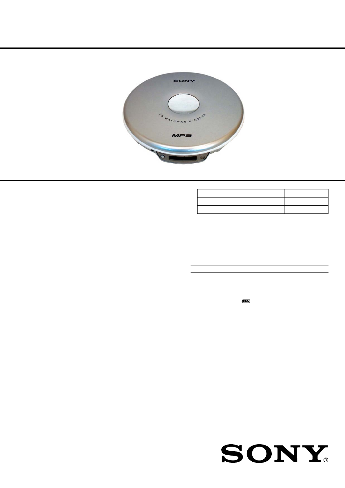
Photo: D-NE006
SPECIFICATIONS
US Model
Canadian Model
AEP Model
D-NE004/NE005/NE006
UK Model
E Model
D-NE005/NE0050/NE006
Australian Model
Tourist Model
Model Name Using Similar Mechanism NEW
CD Mechanism Type
Optical Pick-up Name DAX-25E
CDM-3525A/3525AJ
D-NE005
D-NE004
D-NE005
D-NE006
System
Compact disc digital audio system
Laser diode properties
Emission duration: Continuous
Laser output: Less than 44.6 µW (This output is the value measured at a
distance of 200 mm from the objective lens surface on the optical pick-up
block with 7 mm aperture.)
Power requirements
• Two LR6 (size AA) batteries: 1.5 V DC × 2
• AC power adaptor (DC IN 4.5 V jack):
220 V, 50 Hz (NE005: EE,EU8/NE006: EU8, EE, E18)
120 V, 60 Hz (C&SA, MX)
Dimensions (w/h/d) (without projecting parts and controls)
Approx. 139.8 × 28.8 × 139.8 mm
Mass (excluding accessories)
Approx. 200 g
Operating temperature
5°C - 35°C
MPEG Layer-3 audio coding technology and patents licensed from
Fraunhofer IIS and Thomson.
Design and specifications are subject to change without notice.
Supplied accessories
AC power adaptor (1)
(NE005: EE, EU8/NE0050: C&SA, MX/NE006: EU8, EE, E18)
Headphones (1)
Remote control (1) (supplied with D-NE006 only)
Battery life* (approx. hours)
(When the CD player is used on a flat and stable place.)
Playing time varies depending on how the CD player is used.
When using two Sony alkaline batteries LR6 (SG)
(produced in Japan)
G-PROTECTION G-on G-off
Audio CD 16 11
MP3 CD (Recorded at 128 kbps) 23 23
* Measured value by the standard of JEITA (Japan Electronics and
Information Technology Industries Association).
• The indicator sections of roughly show the remaining battery
power. One section does not always indicate one-fourth of the battery
power.
9-879-861-04
2005L02-1
© 2005.12
PORTABLE CD PLAYER
Sony Corporation
Personal Audio Division
Published by Sony Engineering Corporation

D-NE004/NE005/NE0050/NE006
TABLE OF CONTENTS
1. SERVICING NOTES ................................................ 3
2. GENERAL ................................................................... 3
3. DISASSEMBLY
3-1. Disassembly Flow ........................................................... 4
3-2. Upper Lid Assy, Cabinet (Middle) Assy,
Cabinet (Lower) Assy...................................................... 4
3-3. Optical Pick-Up (CDM-3525A) ...................................... 5
3-4. JACK Board, MAIN Board ............................................. 5
3-5. LPF Board ....................................................................... 6
4. TEST MODE ............................................................... 7
5. ELECTRICAL ADJUSTMENT ............................. 7
6. DIAGRAMS ................................................................. 8
6-1. Block Diagram ................................................................ 9
6-2. Printed Wiring Board
– MAIN Board (Side A), LPF Board (Side A) – ............. 10
6-3. Printed Wiring Board
– MAIN Board (Side B), LPF Board (Side B),
JACK Board – ................................................................. 11
6-4. Schematic Diagram – MAIN Board (1/2),
JACK Board (1/2) – ........................................................ 12
6-5. Schematic Diagram – MAIN Board (2/2), LPF Board,
JACK Board (2/2) – ........................................................ 13
6-6. IC Pin Function Description ............................................ 15
7. EXPLODED VIEWS
7-1. Upper Lid, Cabinet (Middle) Section .............................. 17
7-2. Cabinet (Lower) Section ................................................. 18
8. ELECTRICAL PARTS LIST .................................. 19
Notes on chip component replacement
• Never reuse a disconnected chip component.
• Notice that the minus side of a tantalum capacitor may be
damaged by heat.
Flexible Circuit Board Repairing
• Keep the temperature of the soldering iron around 270 ˚C
during repairing.
• Do not touch the soldering iron on the same conductor of the
circuit board (within 3 times).
• Be careful not to apply force on the conductor when soldering
or unsoldering.
CAUTION
Use of controls or adjustments or performance of procedures
other than those specified herein may result in hazardous radiation
exposure.
UNLEADED SOLDER
Boards requiring use of unleaded solder are printed with the leadfree mark (LF) indicating the solder contains no lead.
(Caution: Some printed circuit boards may not come printed with
the lead free mark due to their particular size)
: LEAD FREE MARK
Unleaded solder has the following characteristics.
• Unleaded solder melts at a temperature about 40 °C higher
than ordinary solder.
Ordinary soldering irons can be used but the iron tip has to be
applied to the solder joint for a slightly longer time.
Soldering irons using a temperature regulator should be set to
about 350 °C.
Caution: The printed pattern (copper foil) may peel away if
the heated tip is applied for too long, so be careful!
• Strong viscosity
Unleaded solder is more viscou-s (sticky, less prone to flow)
than ordinary solder so use caution not to let solder bridges
occur such as on IC pins, etc.
• Usable with ordinary solder
It is best to use only unleaded solder but unleaded solder may
also be added to ordinary solder.
SAFETY-RELATED COMPONENT WARNING!!
COMPONENTS IDENTIFIED BY MARK ! OR DOTTED LINE WITH
MARK !ON THE SCHEMATIC DIAGRAMS AND IN THE PARTS
LIST ARE CRITICAL TO SAFE OPERATION.
REPLACE THESE COMPONENTS WITH SONY PARTS WHOSE
PA RT NUMBERS APPEAR AS SHOWN IN THIS MANUAL OR IN
SUPPLEMENTS PUBLISHED BY SONY.
2
ATTENTION AU COMPOSANT AYANT RAPPORT
À LA SÉCURITÉ!
LES COMPOSANTS IDENTIFÉS PAR UNE MARQUE 0 SUR
LES DIAGRAMMES SCHÉMATIQUES ET LA LISTE DES
PIÈCES SONT CRITIQUES POUR LA SÉCURITÉ DE
FONCTIONNEMENT. NE REMPLACER CES COMPOSANTS
QUE PAR DES PIÈSES SONY DONT LES NUMÉROS SONT
DONNÉS DANS CE MANUEL OU DANS LES SUPPÉMENTS
PUBLIÉS PAR SONY.
SECTION 1
SERVICING NOTES
D-NE004/NE005/NE0050/NE006
Ver. 1.2
NOTES ON HANDLING THE OPTICAL PICK-UP
BLOCK OR BASE UNIT
The laser diode in the optical pick-up block may suffer electrostatic
break-down because of the potential difference generated by the
charged electrostatic load, etc. on clothing and the human body.
During repair, pay attention to electrostatic break-down and also
use the procedure in the printed matter which is included in the
repair parts.
The flexible board is easily damaged and should be handled with
care.
NOTES ON LASER DIODE EMISSION CHECK
The laser beam on this model is concentrated so as to be focused on
the disc reflective surface by the objective lens in the optical pickup block. Therefore, when checking the laser diode emission,
observe from more than 30 cm away from the objective lens.
LASER DIODE AND FOCUS SEARCH OPERATION
CHECK
During normal operation of the equipment, emission of the laser
diode is prohibited unless the upper lid is closed while turning ON
the S811. (push switch type)
The following checking method for the laser diode is operable.
• Method:
Emission of the laser diode is visually checked.
1. Open the upper lid.
2. With a disc not set, turn on the S811 with a screwdriver having
a thin tip as shown in Fig.1.
3. Press the u button.
4. Observing the objective lens, check that the laser diode emits
light.
When the laser diode does not emit light, automatic power
control circuit or optical pick-up is faulty.
In this operation, the objective lens will move up and down 2
times along with inward motion for the focus search.
S811
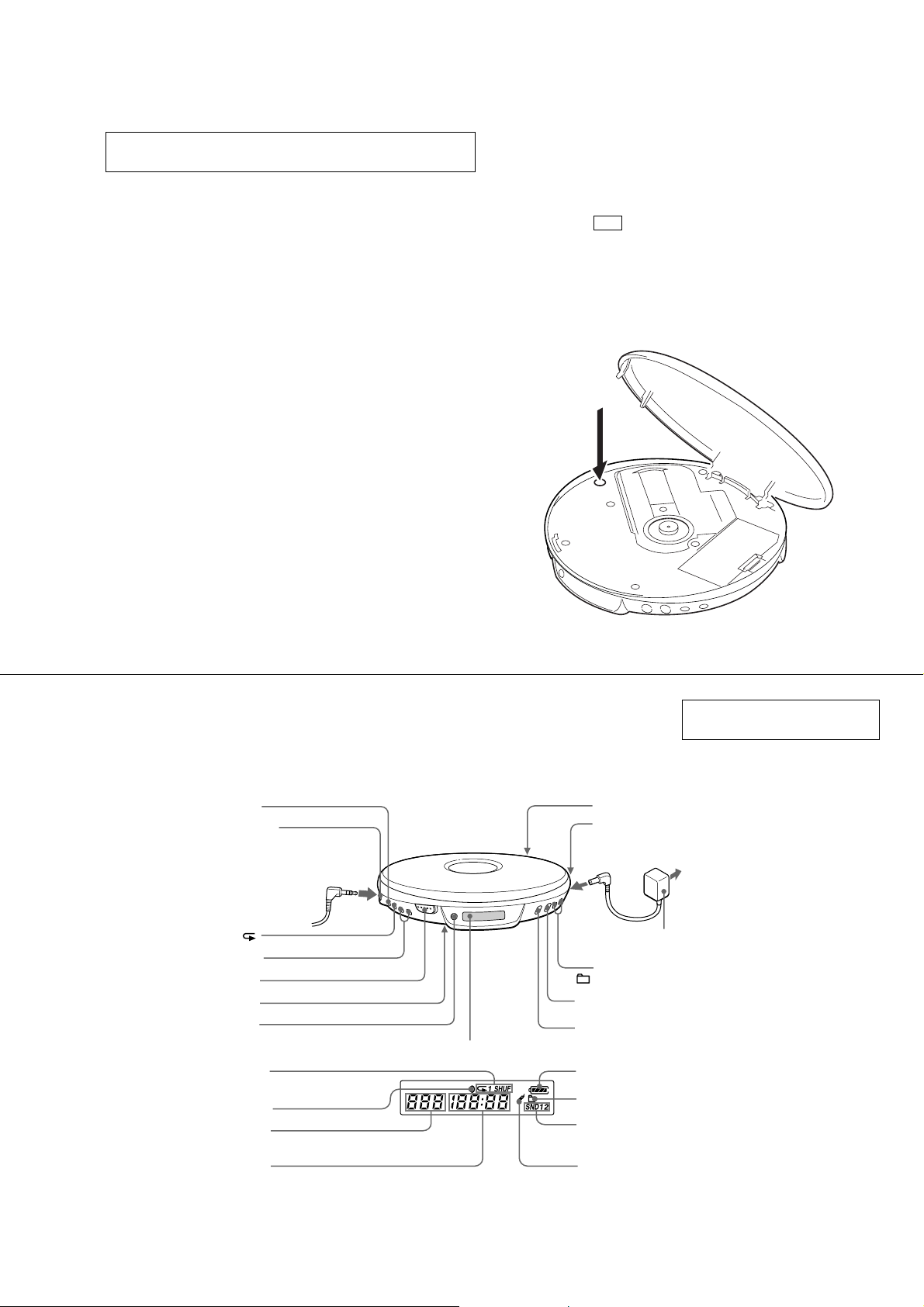
LOCATING THE CONTROLS
SOUND/AVLS
i (headhpones) jack
Headphones
P MODE/
VOL +*/–
OPEN
HOLD (rear)
GROUP
Play mode
SECTION 2
GENERAL
Display
Fig. 1 Method to push the S811
This section is extracted from
instruction manual.
LINE OUT (European and Tourist model only)
DC IN 4.5V
to an AC outlet
AC power adaptor
•
./>
(group)–/+
*(play/pause)
u
(stop)
x
Remaining battery power
MP3 indicator
Track number
Playing time
* The button has a tactile dot.
Group indicator
Sound mode
Bookmark
3
D-NE004/NE005/NE0050/NE006
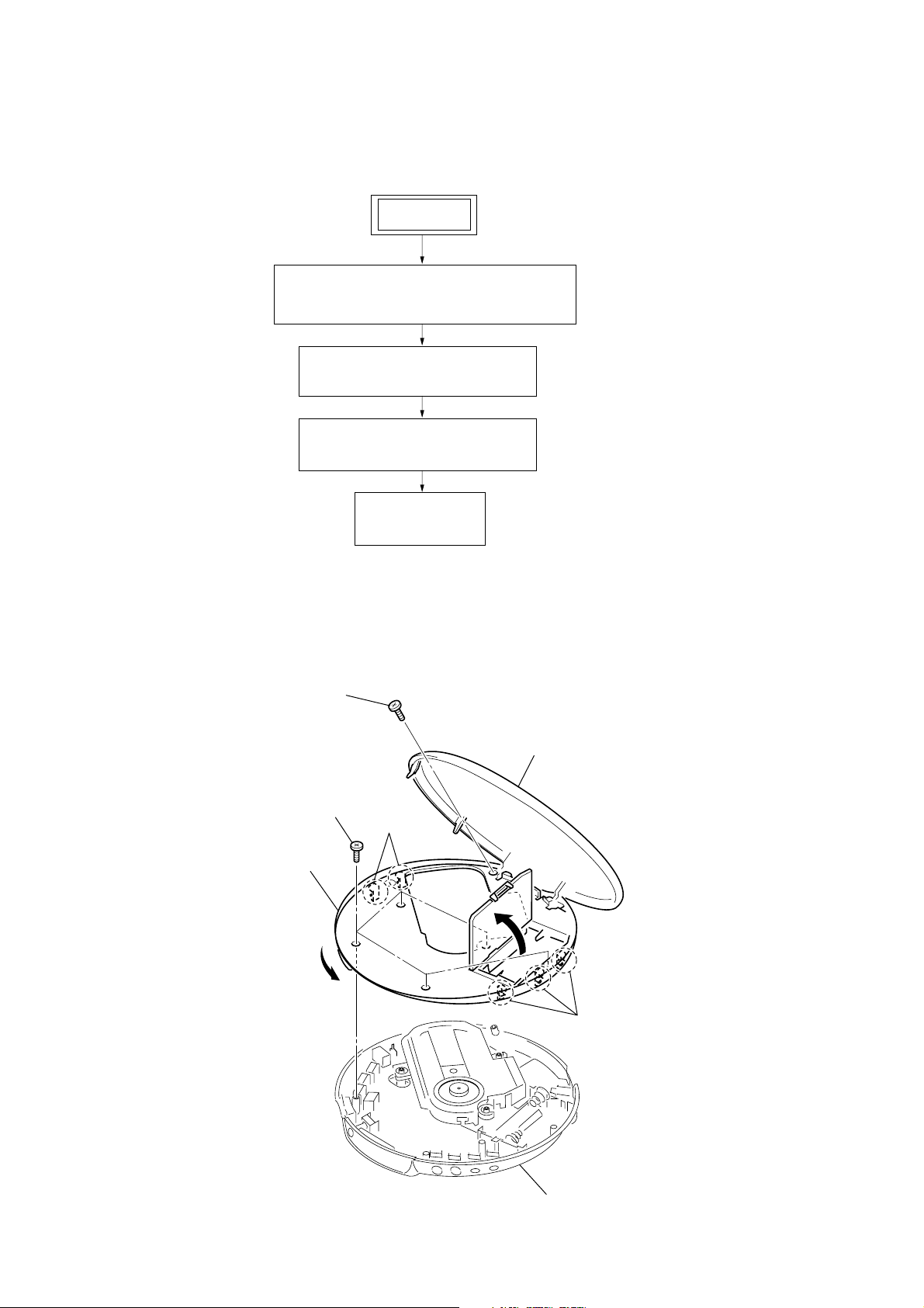
• This set can be disassembled in the order shown below.
3-1. DISASSEMBLY FLOW
3-2. UPPER LID ASSY, CABINET (MIDDLE) ASSY, CABINET (LOWER) ASSY
(Page 4)
3-3. OPTICAL PICK-UP (CDM-3525A)
(Page 5)
3-4. JACK BOARD, MAIN BOARD
(Page 5)
SECTION 3
DISASSEMBLY
SET
3-5. LPF BOARD
(Page 6)
Note: Follow the disassembly procedure in the numerical order given.
3-2. UPPER LID ASSY, CABINET (MIDDLE) ASSY, CABINET (LOWER) ASSY
4
screw
upper lid assy
3
five screws
5
two claws
cabinet (middle) assy
2
1
OPEN
6
three claws
cabinet (lower) assy
4
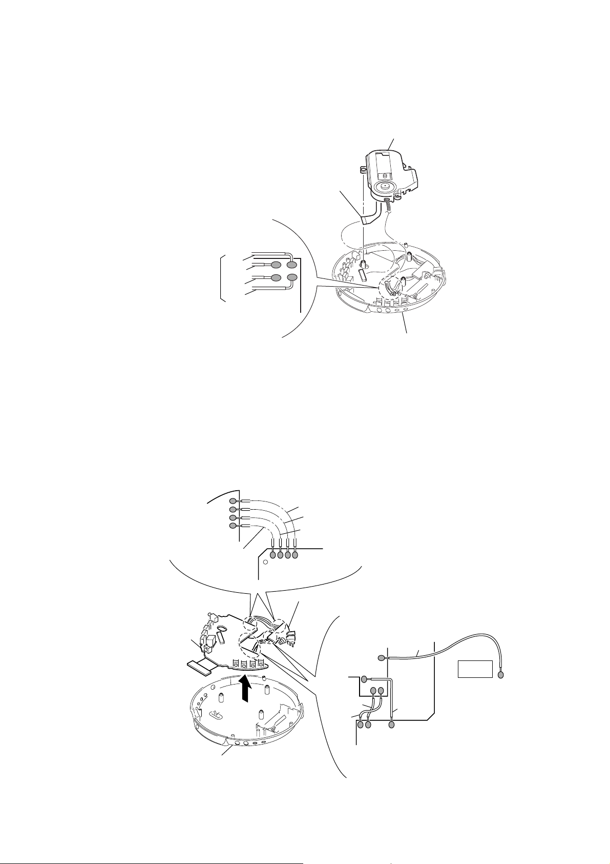
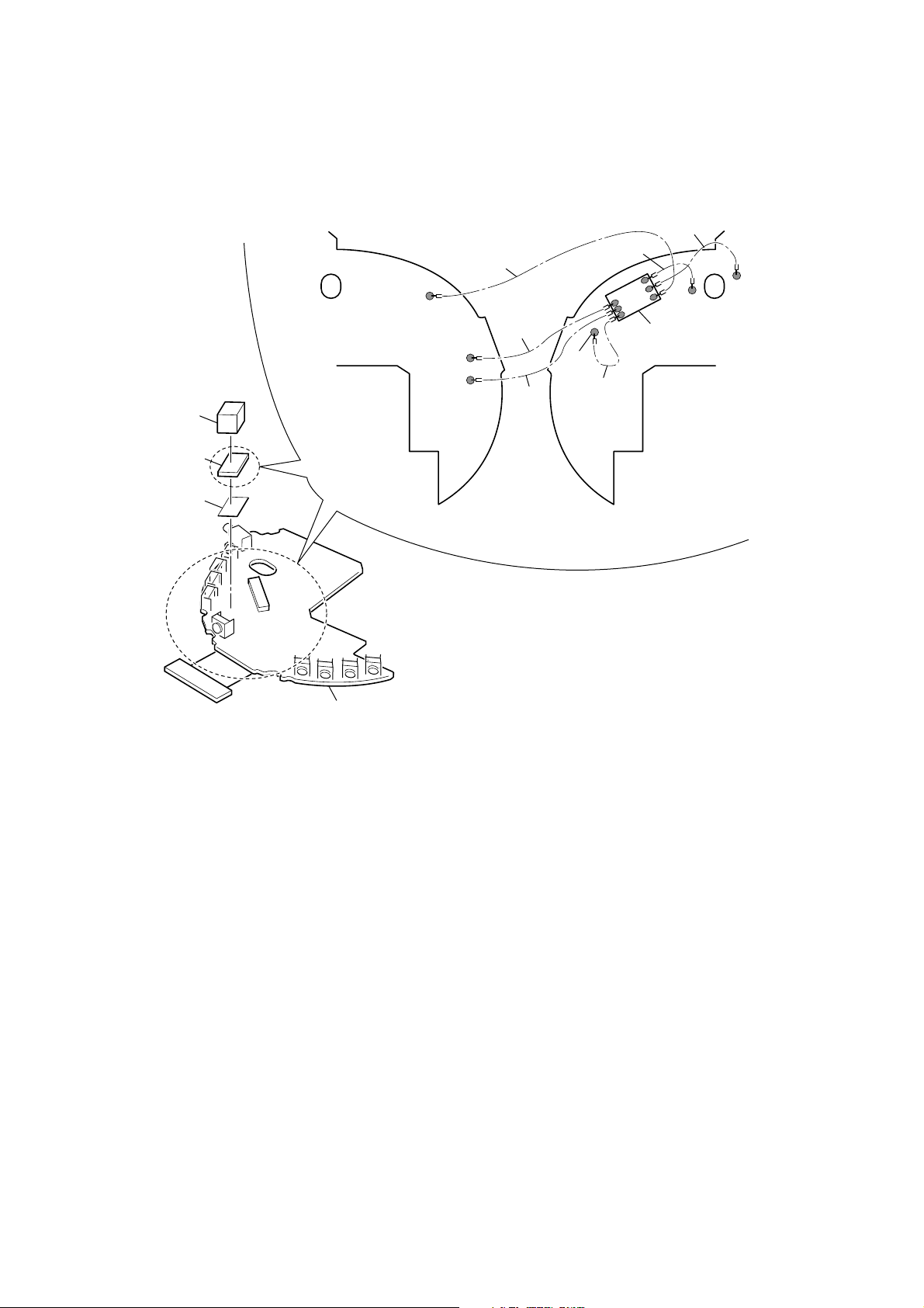
3-3. OPTICAL PICK-UP (CDM-3525A)
)
2
Unsolder four lead wires
1
CN501
D-NE004/NE005/NE0050/NE006
3
optical pick-up (CDM-3525A
To/From
Optical pick-up
(CDM-3525A)
MAIN Board (side A)
3-4. JACK BOARD, MAIN BOARD
3
Unsolder four lead wires (AEP, EE, EU8 only)
JACK Board
(side B)
BLK
ORG
GRY
RED
cabinet (lower) assy
• Abbreviation
EE : East European
EU8 : European model other than UK, EE
and Russian
BLK
GRY
RED
ORG
MAIN Board (side B)
5
MAIN board
1
cabinet (lower) assy
4
JACK board
2
Unsolder four lead wires
JACK Board
(side B)
RED
BLK
WHT
BLU
IC602
26 50
MAIN Board (side B)
125
TP412
SGND
5
D-NE004/NE005/NE0050/NE006
3-5. LPF BOARD
1
Unsolder six lead wires
2
cushion
3
LPF board
C103(+)
TP842
SEG5
TP841
CDM4
WHT
BRN
YEL
TP843
DVDD
ORG
RED
LPF Board
BLK
TP844
RCH
TP307
AUGND2
4
adhesive sheet
MAIN Board
MAIN Board (side B)
MAIN Board (side A)
6
SECTION 4
)
TEST MODE
D-NE004/NE005/NE0050/NE006
SECTION 5
ELECTRICAL ADJUSTMENTS
Procedure:
1. Make a solder bridge to short SL803 (TEST) on the MAIN
board side B.
2. Press the u button.
3. Confirm LCD displays all lights.
4. Confirm the version of the microcomputer will be displayed
in 2 or 3 seconds.
5. To exit this mode, stop supplying power.
6. SL803 is opened by taking the solder bridge.
SL803
(TEST)
(SIDE B)MAIN BOARD
0
C420
1
06
C411
C412
C410
CB414
BATT+
IC401
C403
C404
L401
1
40
C408
R409
C409
21
R802
SL803
(TEST)
61
80
FB801
60
1
TP841
R820
C811
R823
IC801
R829
R835
VDR801
C632
R811
R824
R826
41
40
21
20
R812
C623
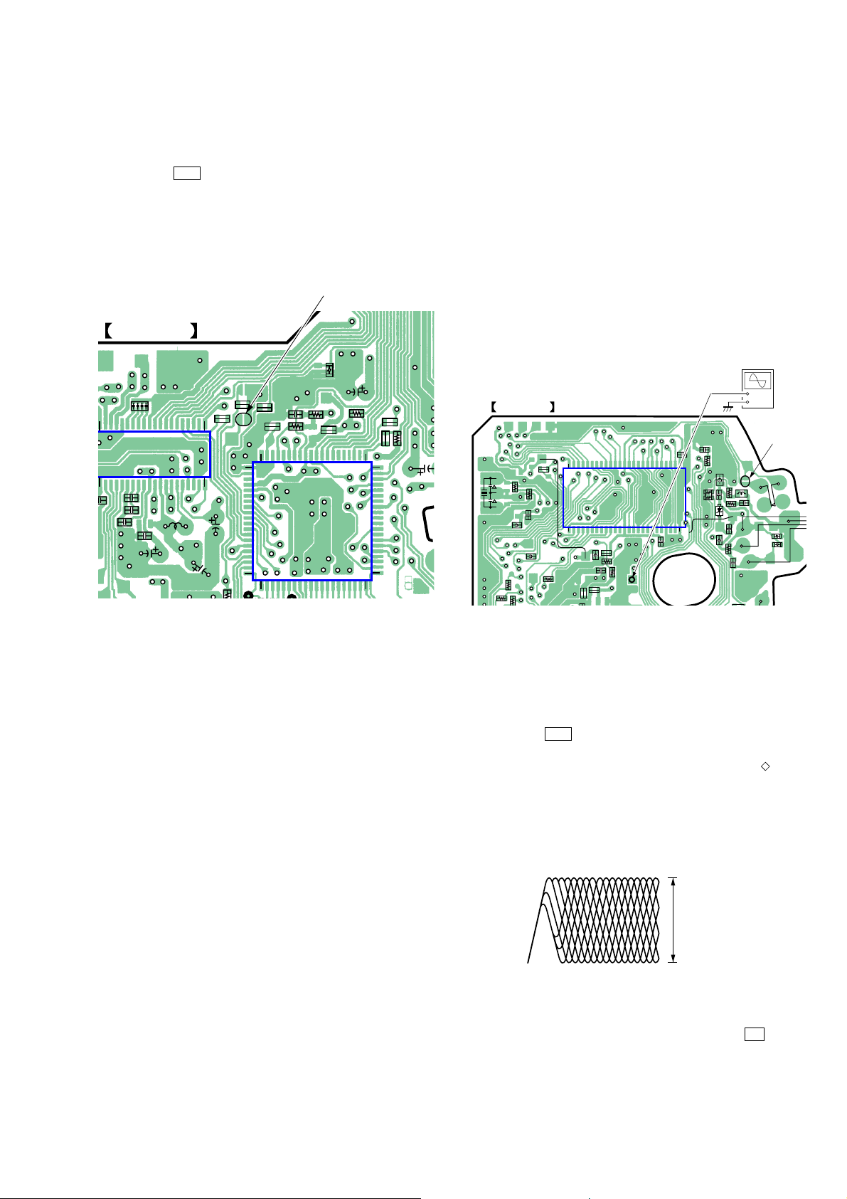
The CD section adjustments are done automatically in this set.
Adjusting Procedure:
1. Perform check in the order given.
2. Use YEDS-18 disc (Part No: 3-702-101-01) unless otherwise
indicated.
3. Power supply voltage requirement :DC4.5 V in DC IN jack.
(J401)
VOLUME button : Minimum
HOLD switch :OFF
Focus Bias Check
Condition:
• Hold the set in horizontal state.
TP604
(RF)
C110
RB301
BLU
R101
D303
FB302
oscilloscope
(AC range)
+
–
SL801
(OPEN)
SL801
(OPEN)
FB301
R111
L101
C308
C106
R102
VDR101
C310
VDR201
R202
C206
S808
Connection:
ORG
RED
X601
R618
FB605
FB401
R416
R418
(SIDE B)MAIN BOARD
GRY
BLK
TP604
(RF)
C627
1
50
C640
BLU
25
R629
C612
R623
R621
2
FB601
R632
R619
IC602
R626
R622
C633
26
BLU
R617
S811
(OPEN)
Procedure:
1. Make a solder bridge to short SL801 (OPEN) on the MAIN
board side B.
2. Connect the oscilloscope to the test point TP604 (RF) on the
MAIN board side B.
3. Set a disc. (YEDS-18)
4. Press the u button.
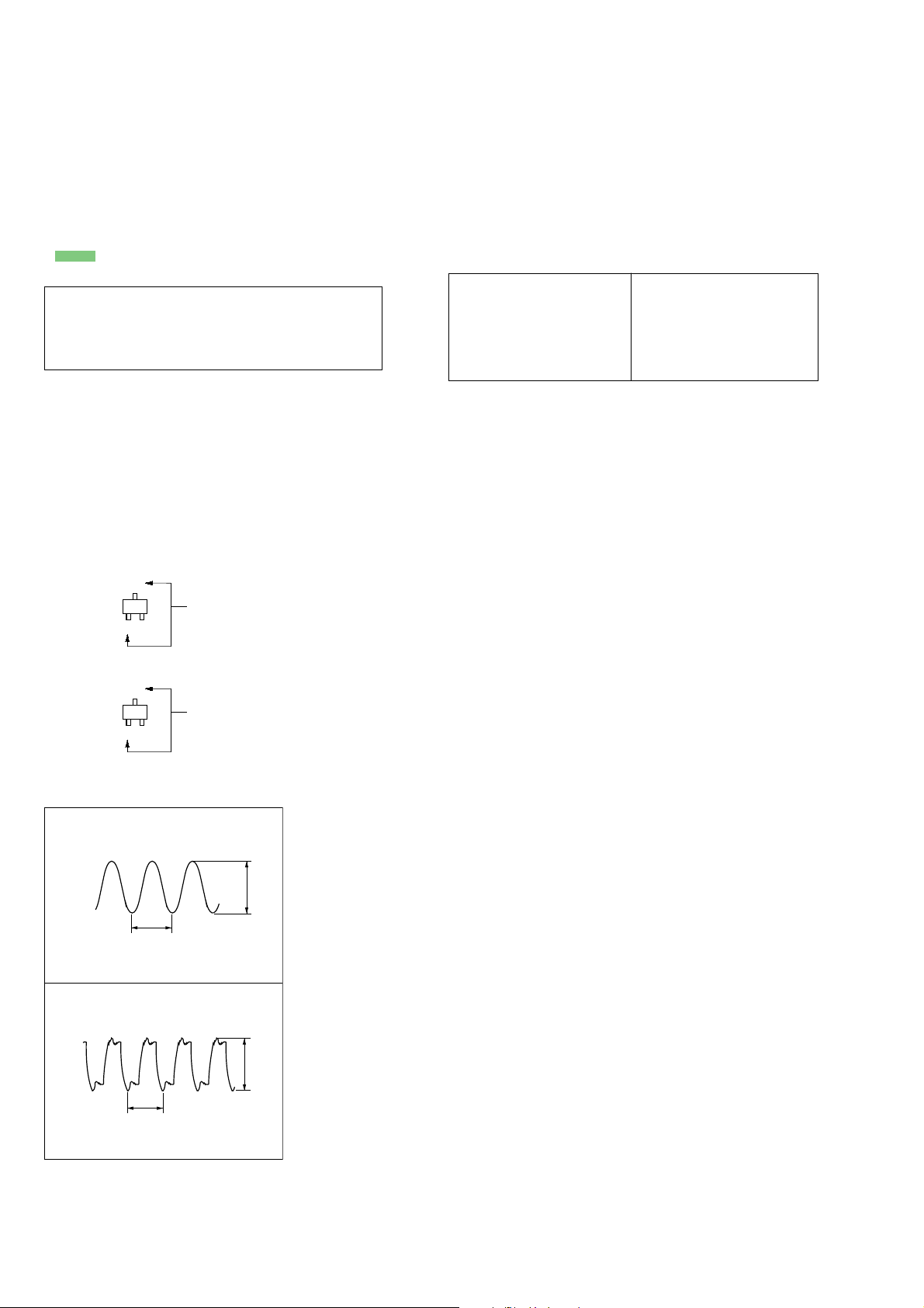
5. Check the oscilloscope waveform is as shown below.
A good eye pattern means that the diamond shape (
) in the
center of the waveform can be clearly distinguished.
RF Signal Reference Waveform (Eye Pattern)
VOLT/DIV : 500 mV (With the 10 : 1 probe in use
TIME/DIV : 500ns
RF level
±
0.2 Vp-p
1.3
To watch the eye pattern, set the oscilloscope to AC range and
increase the vertical sensitivity of the oscilloscope for easy
watch-ing.
6. Stop revolving of the disc motor by pressing the x button.
7. SL801 is opened by taking the solder bridge.
7
D-NE004/NE005/NE0050/NE006
Ver. 1.2
SECTION 6
DIAGRAMS
• Note for Printed Wiring Boards and Schematic Diagrams
Note on Printed Wiring Boards.
• X : parts extracted from the component side.
• Y : parts extracted from the conductor side.
• a : Through hole.
• f : internal component
• : Pattern from the side which enables seeing.
(The other layers' patterns are not indicated.)
Caution:
Pattern face side: Parts on the pattern face side seen from
(Side B) the pattern face are indicated.
Parts face side: Parts on the parts face side seen from
(Side A) the parts face are indicated.
• Abbreviation
8E : General Asian model
AUS : Australian model
CND : Canadian model
E18 : Singaporean, Indian, Malaysian, Vietnamese and South
African model
EU8 : European model other than UK, EE and Russian
EE : East European model
EA : Saudi Arabia model
JE : Tourist model
• Indication of transistor.
C
Q
B
E
D
Q
G
S
These are omitted.
These are omitted.
•Waverforms
Note on Schematic Diagrams.
• All capacitors are in µF unless otherwise noted. (p: pF) 50 WV or
less are not indicated except for electrolytics and tantalums.
• All resistors are in Ω and 1/
• f : internal tolerance.
• C : panel designation.
Note:
The components identified
by mark 0 or dotted line
with mark 0 are critical for
safety.
Replace only with part
number specified.
• A : B+ Line.
• H : adjustment for repair.
• Power voltage is dc 3.3 V and fed with regulated dc power supply
from battery terminal.
•Voltages and waveforms are dc with respect to ground under nosignal conditions.
no mark : CD PLAY
•Voltages are taken with a VOM (Input impedance 10 MΩ).
Voltage variations may be noted due to normal production tolerances.
•Waveforms are taken with a oscilloscope.
Voltage variations may be noted due to normal production tolerances.
• Circled numbers refer to waveforms.
• Signal path.
J : CD PLAY
• Abbreviation
8E : General Asian model
AUS : Australian model
CND : Canadian model
E18 : Singaporean, Indian, Malaysian, Vietnamese and South
African model
EE : East European model
EU8 : European model other than UK, EE and Russian
EA : Saudi Arabia model
JE : Tourist model
4
W or less unless otherwise specified.
Note:
Les composants identifiés
par une marque 0 sont
critiques pour la sécurité.
Ne les remplacer que par une
piéce portant le numéro
spécifié.
IC601 ya XO
1
0.5 V/DIV, 50 ns/DIV
IC801 yd XOUT4M
2
238 ns
1 V/DIV, 0.1 µs/DIV
8
59 ns
1.3 Vp-p
3.4 Vp-p
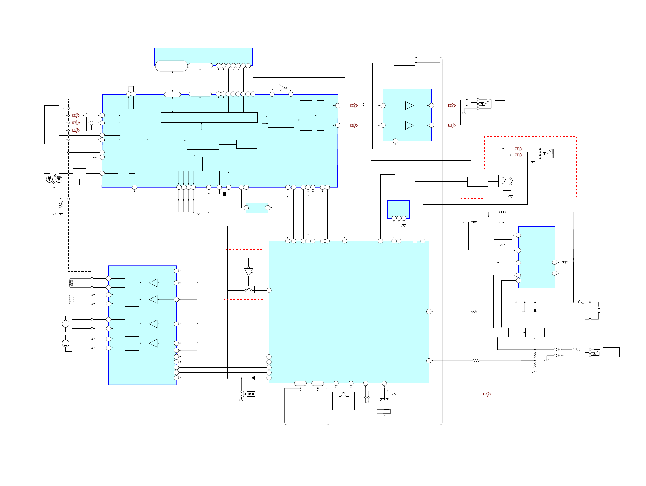
6-1. BLOCK DIAGRAM
D-NE004/NE005/NE0050/NE006
Ver. 1.2
IC602 SDRAM(16M)
OPTICAL
DEVICE
(CDM-3525A/3525AJ)
VCC
OP IC
VC
LD
PD
FOCUS
COIL
TRACKING
COIL
(SLED)
M
(SPINDLE)
M
SEG5
COM4
OUT1
1
OUT2
767
XLINE_DET
XLINEOUT_MUTE
66
BATT+
65
DC IN
DDC
MUTE DRIVE
Q301
L403
SWITCHING
• Signal Path
• Abbreviation
J301
i
AEP, EE, EU8, JE
J302
LINE OUT
Q302
L402
IC401 (2/2)
Q404
SWITCHING
Q403
VG
+VBAT
DC IN DETECT
Q402
: CD PLAY
EE : East European
EU8 : European model other than UK, EE and Russian
DC/DC CONVERTER
SW
37
VSYS
38
VG
36
DCIN
30
31
REGB
+B SWITCH
Q401
D403
PVCC
LG
35
L401
21
F402
F401
DRY BATTERY
SIZE "AA"
(IEC DESIGNATION LR6)
2PCS. 3V
J401
DC IN 4.5V
!
DQ00-07
2,3,5,6,8,9,11,12,39,
40,42,43,45,46,48,49
80 79
RFI
DDC
A
B
C
E
F
LD
DRIVER
Q601
DDC
SLED+
SLED-
SPINDLE+
SPINDLE-
+
F+
F-
T+
T-
BD
3
AC
2
+
E
6
F
7
ASY
10
VBIAS
4
LD
9
18
17
19
20
23
22
25
24
EQO
RF
SIGNAL
GEN.
APC
PD
8
IC401 (1/2)
FOCUS/TRACKING COIL DRIVE,
SLED/SPINDLE MOTOR DRIVE
FO+
DRIVER
FO-
TRK-
DRIVER
TRK+
SLED+
DRIVER
SLED-
SPID+
DRIVER
SPIN-
AMP
AMP
AMP
AMP
SERVO
SIGNAL
GEN.
FOCUS
MUTE34
MUTE1
39,42-48
VREF
TRK
SLED
CLV
CLK
RESET
DQ00-07
DIGITAL SERVO
SIGNAL PROCESSOR
FDOUT
13 14 15 16
FOCUS
11
10
9
8
7
3
4
5
6
2
OFF
1
WP
TDOUT
TRK
FOCUS
19-24,27-32
PROCESSOR
SDOUT
CLVOUT
CLV
SLED
TRK
SLED
CLV
CLK
A0-11
32-21
A00-A11
MP3 &
ADPCM CORE
DIGITAL
SIGNAL
56
17 16 15
34 35 36 37 38
RASX
CLK88
16.9344MHz
CLK
RAS
CASX
CLOCK
OSC
XO
X601
CAS
WEX
XI
60 33 4961
WE
LDQM
14 36
LDQM
NE006
UDQM
CLK
35 34
17 18 19
RCLK
UDQM
16K SRAM
VDD_CORE1
5 1
+VBAT
Q802
Q801
CKE
A13
RCKE
VDD_CORE2
IC603
REG
VOUT
VIN
VG
D803
S801
Q602
7563
FLAG0
AD_MONI0
1 BIT
55
62
CLK
XIN4M
DAC
SUBSYQ
SUBSYQ
SEG1
I
2-21 77-80
CRYSTAL
DISPLAY
X8 OVER
SAMPLING
DIGITAL FILTER
IC601
RF AMP, SERVO,
DIGITAL SIGNAL PROCESSOR,
SDRAM CONTROLLER,
D/A CONVERTER
DDC
WREM
70
MMUTE2
76
75
MMUTE1
57
XRESET
74
XP.OFF
43
K_PLAY
SEG5
MCK
DIN/DOUT
MCK
DIN OUT
SEG20
LCD801
LIQUID
R/W
RW
COM1
LINE
AMP
I
LDACO
RDACO
RESTB
535750515254
XXRESET
COM4
COM4
BUSY
BUSY
KEY MATRIX
S802 – S809
65
KEY1
51
FIFO
IC801
SYSTEM
CONTROL
KEY2
OPEN/CLOSE
4167 68 40
S811
(OPEN)
OFF ON
3
5
56
XHP_MUTE
S812
HOLD
Q101 – 104
HEADPHONE AMP
IN1
IN2
XMUTE
2
IC802
EEPROM
SDA
EE_SDA/REM_SDA
HOLD
L.P.F
IC301
SCL7WP
65
24 382223505349474839
EE_SCL
D-NE004/NE005/NE0050/NE006
99

D-NE004/NE005/NE0050/NE006
Ver. 1.3
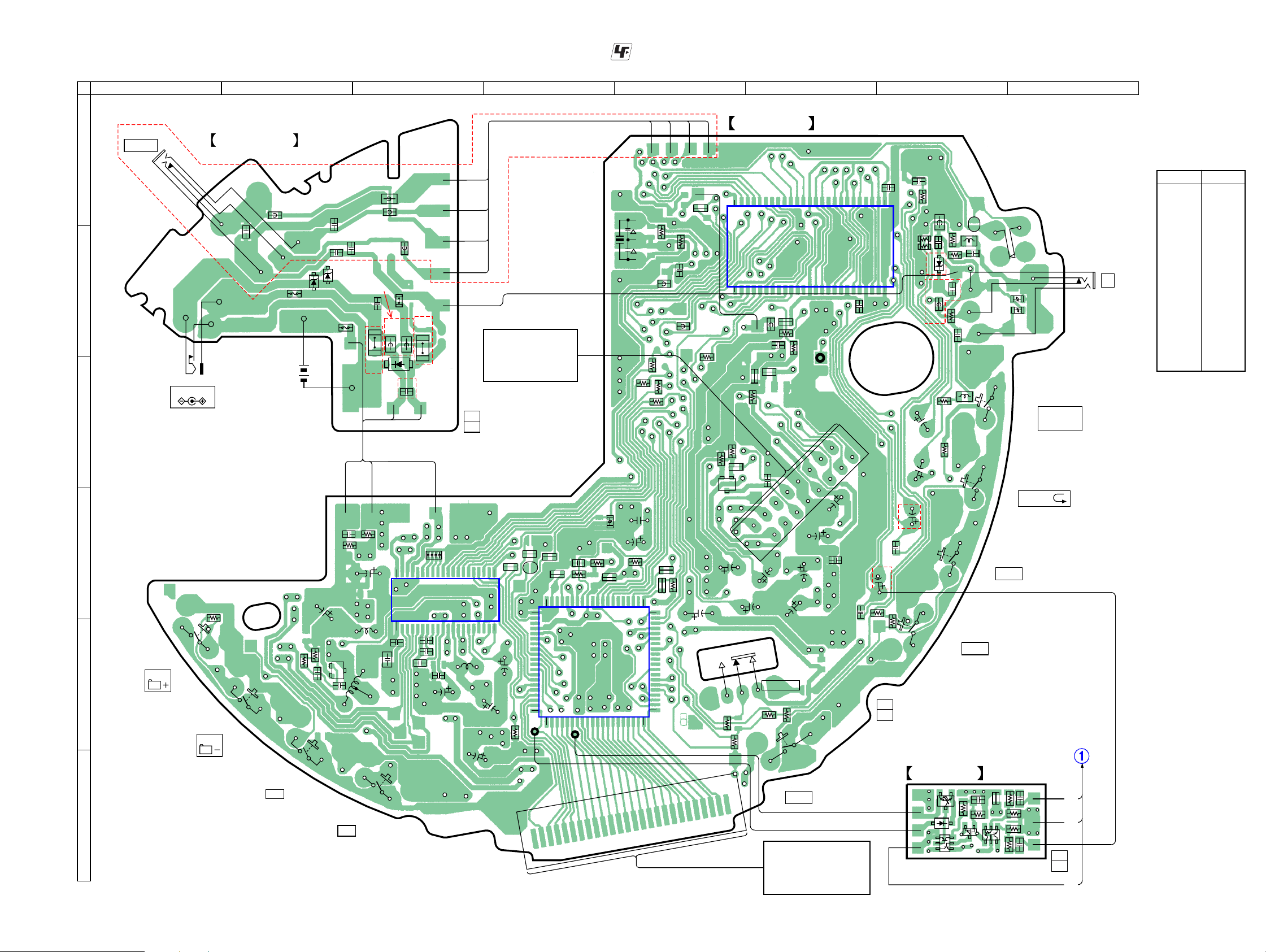
6-2. PRINTED WIRING BOARD – MAIN BOARD (SIDE A), LPF BOARD (SIDE A) –
:Uses unleaded solder.
1
2
3 4 5 6 7
8
(SIDE A)BOARDMAIN
C208
A
MAIN
BOARD
(SIDE B)
(Page 11)
B
< 1 >
C
< 2 >
C210
C301
RB305
R201
BLK
(AUGND2)
8
TP307
D
E
< 3 >
(SIDE A)LPF BOARD
RB302
IC301
E
R304
45
1
Q301
RED
C108
C303
Q302
R204
R104
R103
(AEP,EE,EU8,JE)
R203
TP844
(RCH)
R305R310R311
(AEP,EE,EU8,JE)
C102
C202
C625
E
Q602
RB304
RB620
C201
C641
C630
R308
C624
RB303
C101
R620
FB604
R624
C619
61
C620
R307
C629
C631
80
C618
R601
R615
R309
FB602
60
IC601
1
R613
R608
R607
(NE004:EE/NE005:US,CND,AEP,EE,E,
8E,AUS,EA/NE0050/NE006:EE,E18,JE)
C615
C609
ORG
C604
R614
R630
TP843
(DVDD)
C637
41
40
21
20
C611
R606
R303
C606
C626
C605
IC603
1
C634
34
(NE004:AEP/NE005:EU8/
(AEP,EE,
EU8,JE)
R640
5
NE006:AEP)
1
R808
R804
8
IC802
45
R847
R848
C805
R844
R817
C809
R818
R843
Q801
C812
R410
D810
RB806
D803
(NE006)
(NE006)
R827
Q802
C813
C814
C806
C808
VDR802
R801
C801
R407
E
(NE006)
C802
C807
R404
C413
C428
C405
R422
R406
R810
D403
R405
OPTICAL DEVICE
(CDM-3525A/3525AJ)
(1/2)
(SLED)
+– +–
M
BRN
ORG
L407
L406
Q401
Q402
R403
D401
R424
R862
SLED–
SLED+
(SPINDLE)
BLK
SPINDLE–
SPINDLE+
M
RED
Q403
E
• Semiconductor
Location
Ref. No.
D401 E-6
D403 D-6
D803 D-5
D810 D-5
IC301 A-2
IC601 B-3
IC603 C-4
IC802 E-4
Q301 B-2
Q302 B-2
Q401 D-6
Q402 E-6
Q403 E-7
Q602 B-3
Q801 D-5
Q802 E-7
VDR802 E-5
Location
F
D-NE004/NE005/NE0050/NE006
1-868-890-
11
(11)
1-867-954-
1010
R850
12
(12)
6-3. PRINTED WIRING BOARD – MAIN BOARD (SIDE B), LPF BOARD (SIDE B), JACK BOARD –
D-NE004/NE005/NE0050/NE006
Ver. 1.3
:Uses unleaded solder.
S809
S808
SOUND/
AVLS
BLK
RED
WHT
11
(11)
8
MAIN
BOARD
(SIDE A)
(Page 10)
< 1 >
< 2 >
< 3 >
J301
i
• Semiconductor
Location
Ref. No.
D101 F-7
D303 B-7
D402 C-3
D404 B-2
D406 B-2
IC401 D-3
IC602 B-6
IC801 E-4
Q101 F-7
Q102 F-7
Q103 F-7
Q104 F-7
Q404 E-2
Q601 C-5
VDR801 D-5
Location
1
(AEP,EE,EU8,JE)
J302
LINE OUT
2
JACK BOARD
3 4 5 6 7
(SIDE B)MAIN BOARD
ORG
RED
GRY
BLK
A
BLK
15
16
C607
C105
1-867-954-
C627
C640
(AEP,EE,EU8,JE)
R853
C633
FB401
R812
R629
R622
C623
BLU
R617
25
IC602
26
BLU
R632
FB601
R619
C612
R621
R623
R602
R604
R603
R605
E
Q601
C601
R828
1
C603
1
2
C610
C628
HOLD
ON
R846
R845
S812
T
.
OFF
S806
GROUP
C305
S806
R854
R626
TP604
C304
(RF)
C602
CN501
C402
LCD801
LIQUID CRYSTAL
DISPLAY
C427
L408
RED
DC IN+
C407
S807
FB303
FB202
FB304
(AEP,EE,EU8,JE)
L404
(AEP,EE,EU8,JE)
D402
C421
DC IN+
RED
20
C420
21
C406
C412
C411
R420
L405
BLK
C410
L409
DC IN–
1-867-955-
CB414
FB102
C109
B
DRY BATTERY
J401
DC IN 4.5V
SIZE "AA"
(IEC DESIGNATION LR6)
2PCS. 3V
F402
CN401
C209
C309
D406
(AEP,EE,EU8,JE)
F401
C306
D404
(EXCEPT AEP,EE,EU8,JE)
BATT+
WHT
CN402
C
BLK
DC IN–
C401
R401
C417
C416
C419
R415
E
R402
C420
L403
Q404
L402
S807
x
D
R849
S802
S802
>
E
S803
.
S803
S801
u
R414
S801
F
WHT
BATT+
IC401
C403
C404
GRY
RED
ORG
BLU
OPTICAL DEVICE
(CDM-3525A/3525AJ)
11
(11)
R409
1
40
L401
C810
C409
C408
R821
(2/2)
R802
SL803
(TEST)
61
80
FB801
R820
60
1
TP841
(CDM4)
YEL
22
C811
R823
R829
IC801
TP842
(SEG5)
BRN
R835
X601
CN801
R417
VDR801
C632
R811
FB605
41
20
R416
R419
C642
R618
R418
R824
R826
40
21
C110
1
(NE006)
BLU
50
C204
(AEP,EE,EU8,JE)
C203
C205
C103
WHT
S805
R852
12
(12)
TP103
BRN
TP102
YEL
TP101
ORG
R101
SL801
FB301
(OPEN)
R111
C308
RB301
R102
D303
C310
FB302
R211
S804
R202
C206
S808
L201
R851
S809
S805
VOL–
(NE006)
C104
LPF BOARD
Q101
R101
Q103
Q102
C102
R102
D101
L101
C106
VDR101
VDR201
S804
VOL+
(SIDE B)
R108
R105
R106
R107
Q104
R104
S811
(OPEN)
P MODE/
TP105
C105
TP106
TP104
C104
1-868-890-
D-NE004/NE005/NE0050/NE006
1111
 Loading...