

Page 1
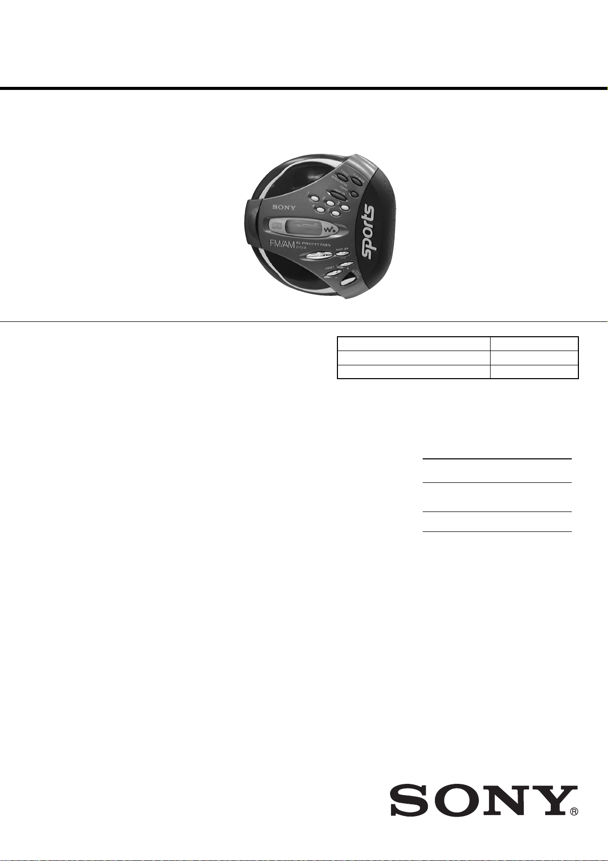
D-FS18
SERVICE MANUAL
Ver. 1.1 2005.07
SPECIFICATIONS
CD player
System
Compact disc digital audio system
Laser diode properties
Material: GaAlAs
Wavelength: λ = 780 nm
Emission duration: Continuous
Laser output: Less than 44.6 µW
(This output is the value measured at a distance
of 200 mm from the objective lens surface on
the optical pick-up block with 7 mm aperture.)
D-A conversion
1-bit quartz time-axis control
Frequency response
40 - 20 000 Hz
307)
Output (at 4.5 V input level)
Headphones (stereo minijack)
Approx. 5 mW + Approx. 5 mW at 16 Ω
+1–4
dB (measured by EIAJ CP-
Radio
Frequency range (STEP switch)
9 kHz step:
FM: 87.5 - 108.0 MHz
AM: 531 - 1 710 kHz
10 kHz step:
FM: 87.5 - 108.0 MHz
AM: 530 - 1 710 kHz
Antenna
FM: Headphones cord antenna
AM: Built-in ferrite bar antenna
General
Power requirements
For the area code of the model you
purchased, check the upper left side of the
bar code on the package.
• Sony NH-WM2AA rechargeable batteries:
2.4 V DC
•Two LR6 (size AA) batteries: 3 V DC
•AC power adaptor (DC IN 4.5 V jack):
U2/U/CA2/E92/MX2/TW2/BR3 model:
120 V, 60 Hz
CED/CET/CEW/CEX/CE7/EE/EE1/E13/G5/
G6/G7/G8/BR1 model:
220 - 230 V, 50/60 Hz
CEK/3CE7 model: 230 - 240 V, 50 Hz
AU2 model: 240 V, 50 Hz
JE.W/E33/EA3 model: 100 - 240 V, 50/60 Hz
HK2 model: 220 V, 50/60 Hz
AR1/CNA model: 220 V, 50 Hz
• Sony DCC-E345 car battery cord for use on
car battery: 4.5 V DC
US Model
Canadian Model
Model Name Using Similar Mechanism D-E770/EJ711/EJ715
CD Mechanism Type CDM-3123EBA
Optical Pick-up Type DAX-23E
Battery life* (approx. hours)
(When you use the CD player on a flat and stable
surface.)
Playing time varies depending on how the CD
player is used.
When using G-PROTECTION Radio
NH-WM2AA 18 21 38
(charged for
about 5 hours**)
Two Sony alkaline 31 35 66
batteries LR6(SG)
*Measured value by the standard of EIAJ
(Electronic Industries Association of Japan).
** Charging time varies depending on how the
rechargeable battery is used.
Operating temperature
5°C - 35°C (41°F - 95°F)
Dimensions (w/h/d) (excluding
projecting parts and controls)
Approx. 146 × 38 × 136 mm
3
⁄4 × 1 1⁄2 × 5
(5
Mass (excluding accessories)
Approx. 363 g (12.9 oz.)
on off on
3
⁄8 in.)
— Continued on next page —
9-873-122-12
2005G16-1
© 2005.07
FM/AM PORTABLE CD PLAYER
Sony Corporation
Personal Audio Group
Published by Sony Engineering Corporation
Page 2

D-FS18
Supplied accessories
For the area code of the location in which you
purchased the CD player, check the upper left side
of the bar code on the package.
AC power adaptor (1)
Headphones (1)
Hand strap (1)
For US customers
The AC power adaptor supplied is not intended to
be serviced. Should the AC power adaptor cease to
function in its intended manner, during the warranty
period, the adaptor should be returned to your
nearest Sony Service Center or Sony Authorized
Repair Center for replacement, or after warranty
period, it should be discarded.
Optional accessories
AC power adaptor AC-E45HG
Active speaker system SRS-Z500
SRS-T1
Car battery cord DCC-E345
Car battery cord with car connecting pack
DCC-E34CP
Car connecting pack CPA-9C
Connecting cord RK-G129
RK-G136
Rechargeable battery NH-WM2AA
Earphones MDR-E848LP
MDR-EX70LP
Headphones MDR-A44L
MDR-A110LP
Your dealer may not handle some of the
above listed accessories. Please ask the
dealer for detailed information about the
accessories in your country.
TABLE OF CONTENTS
1. SERVICING NOTES ······················································· 3
2. GENERAL ·································································· 4
3. DISASSEMBLY
3-1. Cabinet (Lower) Sub ASSY,
Cabinet (Inner) Sub Assy, Main Board ································ 5
3-2. MD ASSY············································································ 5
3-3. Motor ASSY, Turn Table (Spindle) (M902) ························ 6
3-4. Optical Pick-up (DAX-23E),
Motor Assy (Sled) (M901) ···········································6
3-5. “Lid, Upper”, Switch Unit ···················································7
4. ELECTRICAL ADJUSTMENS ···································· 8
5. DIAGRAMS
5-1. BLOCK DIAGRAM CD SECTION ······························· 10
TUNER SECTION ···························································· 11
5-2. PRINTED WIRING BOARD
MAIN (SIDE A) SECTION ·········································12
5-3. PRINTED WIRING BOARD
MAIN (SIDE B) SECTION ········································· 13
5-4. SCHEMATIC DIAGRAM TUNER SECTION ··············14
5-5. SCHEMATIC DIAGRAM CD SECTION (1/4) ·············15
5-6. SCHEMATIC DIAGRAM CD SECTION (2/4) ·············16
5-7. SCHEMATIC DIAGRAM CD SECTION (3/4) ·············17
5-8. SCHEMATIC DIAGRAM CD SECTION (4/4) ·············18
5-9. IC PIN FUNCTION DESCRIOTION ······························· 19
5-10.IC BLOCK DIAGRAMS ·················································· 23
6. EXPLODED VIEWS
6-1. CABINET SECTION ························································ 26
6-2. MECHANISM SECTION (CDM-3123EBA)··················· 27
DANGER
Invisible laser radiation when open and interlock failed or defeated.
Avoid direct exposure to beam.
CAUTION
Use of controls or adjustments or performance of procedures other
than those specified herein may result in hazardous radiation
exposure.
Flexible Circuit Board Repairing
• K eep the temperature of the soldering iron around 270°C during
repairing.
• Do not touch the soldering iron on the same conductor of the
circuit board (within 3 times).
• Be careful not to apply force on the conductor when soldering or
unsoldering.
Notes on chip component replacement
• Never reuse a disconnected chip component.
• Notice that the minus side of a tantalum capacitor may be dam-
aged by heat.
7. ELECTRICAL PARTS LIST········································· 28
SAFETY-RELATED COMPONENT WARNING!!
COMPONENTS IDENTIFIED BY MARK 0 OR DOTTED LINE
WITH MARK 0 ON THE SCHEMATIC DIAGRAMS AND IN THE
PARTS LIST ARE CRITICAL TO SAFE OPERATION.
REPLACE THESE COMPONENTS WITH SONY PARTS WHOSE
PART NUMBERS APPEAR AS SHOWN IN THIS MANUAL OR IN
SUPPLEMENTS PUBLISHED BY SONY.
ATTENTION AU COMPOSANT AYANT RAPPORT
À LA SÉCURITÉ!
LES COMPOSANTS IDENTIFIÉS PAR UNE MARQUE 0 SUR LES
DIAGRAMMES SCHÉMATIQUES ET LA LISTE DES PIÈCES
SONT CRITIQUES POUR LA SÉCURITÉ DE FONCTIONNEMENT.
NE REMPLACER CES COMPOSANTS QUE PAR DES PIÈCES
SONY DONT LES NUMÉROS SONT DONNÉS DANS CE MANUEL
OU DANS LES SUPPLÉMENTS PUBLIÉS PAR SONY.
2
Page 3
SECTION 1
MAIN board
S801
SERVICING NOTES
D-FS18
NOTES ON HANDLING THE OPTICAL PICK-UP BLOCK OR
BASE UNIT
The laser diode in the optical pick-up block may suffer electrostatic
breakdown because of the potential difference generated by the charged
electrostatic load, etc. on clothing and the human body. During re pair, pay
attention to electrostatic breakdown and also use the procedure in the printed
matter which is included in the repair parts.
The flexible board is easily damaged and should be handled with care.
NOTES ON LASER DIODE EMISSION CHECK
The laser beam on this model is concentrated so as to be focused on the disc
reflective surface by the objectiv e lens in the optical pick-up block. Therefore,
when checking the laser diode emission, observe from more than 30cm away
from the objective lens.
Before Replacing the Optical pick-up Block
Please be sure to check thoroughly the parameters as per the “Optical pickup Block Checking Procedure” (Part No. : 9-960-027-11) issued separately
before replacing the optical Pick-up block.
Note and specifications required to check are given below.
• FOK output : IC601 eg pin
When checking FOK, remove the lead wire to disc motor.
• RF signal P-to-P value : 0.4 to 0.5Vp-p
Precautions for Checking Emission of Laser Diode
Laser light of the equipment is focused by the object lens in the optical
pick-up so that the light focuses on the reflection surface of the disc.
Therefore, be sure to keep your eyes more then 30 cm apart from the object
lens when you check the emission of laser diode.
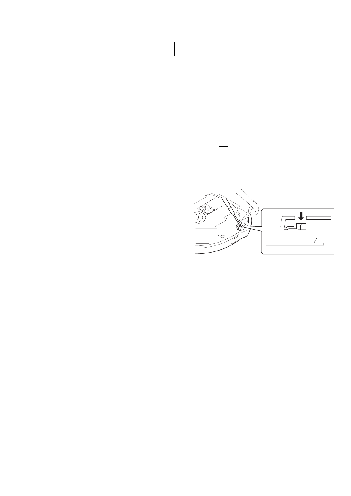
Laser Diode Checking Methods
During normal operation of the equipment, emission of the laser diode is
prohibited unless the upper lid is closed while turning ON the S801. (push
switch type)
The following two checking methods for the laser diode are oper-able.
• Method:
Emission of the laser diode is visually checked.
1. Open the upper lid.
2. W ith a disc not set, turn on the S801 with a scre wdriv er having a thin tip
as shown in Fig.1.
Note: Do not push the detection lever strongly , or it may be bent or dam-
aged.
3. Press the u button.
4. Observing the objective lens, check that the laser diode emits light.
When the laser diode does not emit light, automatic power control circuit
or optical pickup is faulty.
In this operation, the objective lens will move up and do wn 5 times along
with inward motion for the focus search.
Fig.1 Method to push S801
3
Page 4
D-FS18
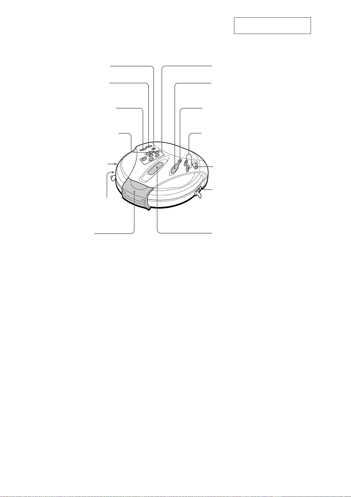
CD player (front)
SECTION 2
GENERAL
This section is extracted from
instruction manual.
1 SOUND button
2 PLAY MODE•
TUNING + button
3 REPEAT/ENTER•
TUNING – button
4 RADIO ON•BAND
button
5 VOL(volume)
control
6 i(headphones)
jack
7 Buckle
8 1-5buttons
9 u (play/pause)
button
q; x (stop)/CHG (charge)•
RADIO OFF button
qa ./>
(AMS/search) •
PRESET –/+
buttons
qs HOLD switch
qd DC IN 4.5 V
(external power
input) jack
qf Display
4
Page 5
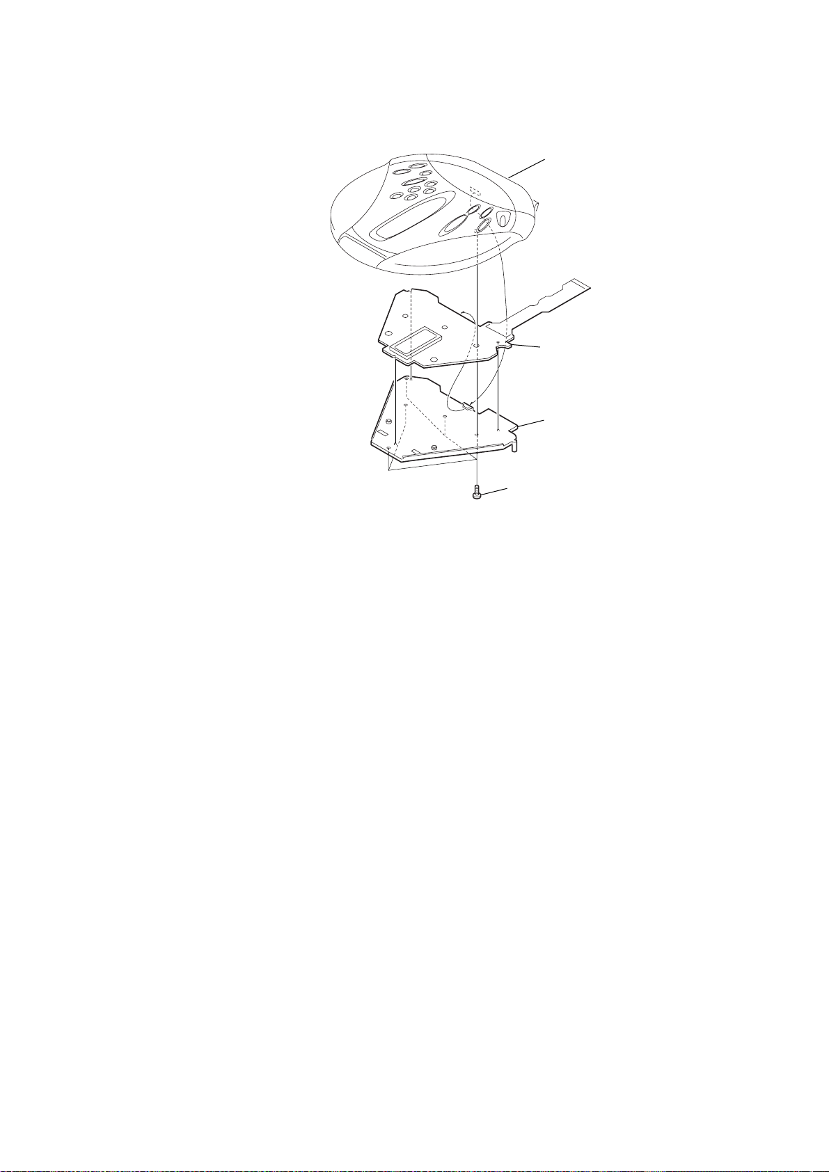
DISASSEMBLY
)
z
The equipment can be removed using the following procedure.
D-FS18
SECTION 3
Set
Cabinet (lower) sub ASSY, Cabinet (inner) sub ASSY, Main board MD ASSY
Cabinet (front)
“Lid, Upper”, Switch unit
Motor ASSY, Turn table (Spindle) (M902),
Optical pick-up (DAX-23E), Motor ASSY (Sled) (M901
Note : Follow the disassembly procedure in the numerical order given.
3-1. CABINET (LOWER) SUB ASSY, CABINET (INNER) SUB ASSY, MAIN BOARD
Five screws (B2)
5
6
Claws
7
MAIN board
9
Cabinet (Inner) sub assy
Lid, Upper
3-2. MD ASSY
2
Screw, tapping
CN502 (Green)
2
CN503 (White)
1
3
Optical pick-up flexible board
3
Screw, (B2)
2
Screw, tapping
MD ASSY
8
4
Switching arm assy
1
Screw, step
Main board
Flexible board (CN801)
4
5
Page 6
D-FS18
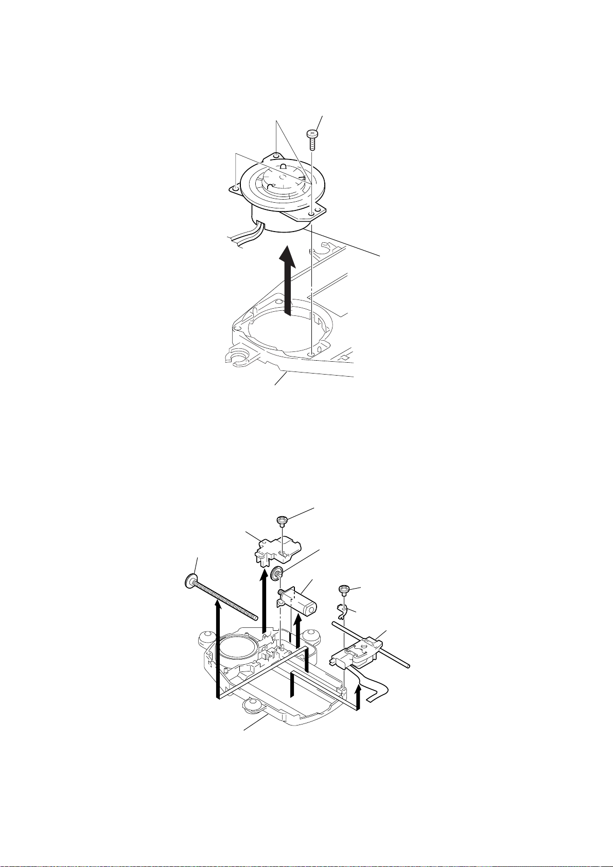
3-3. MOTOR ASSY, TURN TABLE (SPINDLE) (M902)
1
Screws
(B1.7x5)
2
Chassis
3-4. OPTICAL PICK-UP (DAX-23E), MOTOR ASSY (SLED) (M901)
Screw (B 1.7x5)
1
Cover, Gear
Screw (feed) assy
Gear B
Motor ASSY, Turn tabl
(Spindle) (M902)
Motor ASSY (Sled) (M901)
2
5
3
Chassis
4
Screw
(P 1.4x3.5)
Bracket (Shaft)
6
Optical pick-up
(DAX-23E)
6
Page 7
3-5. “LID, UPPER”, SWITCH UNIT
4
2
Lid, Upper
Switch unit
5
Cover, Lid
3
D-FS18
Five screws (B 1.7
1
×
3.5)
7
Page 8
D-FS18
)
SECTION 4
ELECTRICAL ADJUSTMENTS
CD SECTION
The CD section adjustments are done automatically in this set.
Precautions for Check
1. Perform check in the order given.
2. Use YEDS-18 disc (Part No.: 3-702-101-01) unless otherwise
indicated.
3. Power supply voltage requirement : DC4.5 V in DC IN jack.
(J401)
VOLUME : Minimum
AVLS : NORM
HOLD : OFF
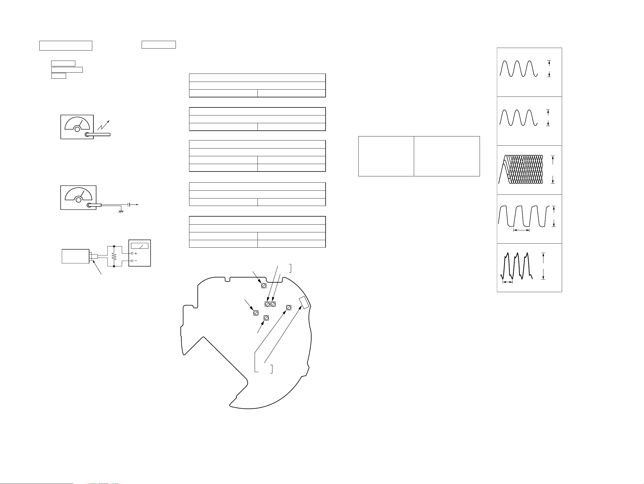
Focus bias Check
Condition:
• Hold the set in horizontal state.
• Terminate TAP802 (open) by solder.
Connection:
Oscilloscope
(AC range)
2 K Ω
TJ635 (GND)
[MAIN BOARD] (Side B)
TJ629 (RF)
Procedure:
1. Connect the oscilloscope to the test points TJ629 (RF) and TJ635
(GND) on the MAIN board.
2. Set a disc. (YEDS-18)
3. Press the u button.
4. Check the oscilloscope waveform is as shown below.
A good eye pattern means that the diamond shape (◊) in the
center of the waveform can be clearly distinguished.
RF Signal reference Waveform (Eye Pattern)
VOLT/DIV : 100 mV (With the 10 : 1 probe in use
TIME/DIV : 500ns
RF level
0.4 to 0.5 Vp-p
To watch the eye pattern, set the oscilloscope to AC range and
increase the vertical sensitivity of the oscilloscope for easy
watch-ing.
5. Stop revolving of the disc motor by pressing the x button.
8
Page 9
N
r
SECTION 5
DIAGRAMS
D-FS18
TUNER SECTION
• Switch Location
VOLUME : MAX
MEGA BASS : OFF
AVLS : NORMAL
[AM]
BAND: AM
AM RF signal
generator
30% amplitude modulation by 400Hz
signal.
Output level : as low as possible
[FM]
BAND : FM
FM RF signal
generator
75kHz(100%) amplitude modulation
by 1kHz signal.
Output level: as low as possible
set
16 Ω
i jack (J302)
Put the lead-wire
antenna close to
the set.
0.01µF
FM I
point
level mete
0 dB = 1 µV
• Repeat the procedures in each adjustment several times for the
maximum level meter indication.
• The frequency coverage and tracking adjustments should be
finally done by the trimmer capacitors.
AM IF ADJUSTMENT
Adjust for a maximum reading on level meter.
T1 450kHz
AM FREQUENCY COVERAGE ADJUSTMENT
Adjust for a maximum reading on level meter.
L4 520kHz
AM TRACKING ADJUSTMENT
Adjust for a maximum reading on level meter.
L3 620kHz
CT3 1,400kHz
FM FREQUENCY COVERAGE ADJUSTMENT
Adjust for a maximum reading on level meter.
L2 86.5MHz
FM TRACKING ADJUSTMENT
Adjust for a maximum reading on level meter.
L1 86.5MHz
CT1 109.5MHz
Adjustment Location: Main board
FM TRACKING
T1 AM IF adjustment
L2 FM FREQUENCY
COVERAGE
adjustment
L1
CT1
adjustment
Note on Printed Wiring Board:
• X : parts extracted from the component side.
• b : Pattern from the side which enables seeing.
Note on Schematic Diagrams:
• All capacitors are in µF unless otherwise noted. pF: µµF
50 WV or less are not indicated except for electrolytics
and tantalums.
• All resistors are in Ω and 1/
specified.
¢
•
• 2 : nonflammable resistor.
• C : panel designation.
• H : adjustment for repair.
• A : B+ Line.
• Voltages and waveforms are dc with respect to ground
Note:
The components identified by mark 0 or dotted
line with mark 0 are critical for safety.
Replace only with part
number specified.
• Voltages are taken with a VOM (Input impedance 10 MΩ).
• Signal path.
• Abbreviation
: internal component.
under no-signal (detuned) conditions.
no mark : FM
( ) : AM
< > : CD
Voltage variations may be noted due to normal production tolerances.
F : FM
f : AM
J : CD
CND : Canadian model
4
W or less unless otherwise
Note:
Les composants identifiés par
une marque 0 sont critiques
pour la sécurité.
Ne les remplacer que par une
piéce portant le numéro
spécifié.
• Waveforms
1
IC601 of XTAO
16.9MHz
2
IC801 ul XIN
4MHz
3
IC601 ua RFAC
4
IC61 uf XOUT
µ
13.3
5
T81 C86
480 nsec
2.3 Vp-p
VOLT/DIV: 1.2 V AC
TIME/DV: 20 nsec
3.6 Vp-p
VOLT/DIV: 0.1 V AC
TIME/DV: 0.1 µsec
400 – 500
mVp-p
VOLT/DIV: 0.1 V AC
TIME/DV: 0.1 µsec
sec
VOLT/DIV: 1.2 V AC
TIME/DV: 10 µsec
30 Vp-p
VOLT/DIV: 10 V AC
TIME/DV: 0.2 µsec
2.4 Vp-p
L4 AM FREQUENCY
COVERAGE
adjustment
L3
AM TRACKING
CT3
adjustment
99
Page 10
D-FS18
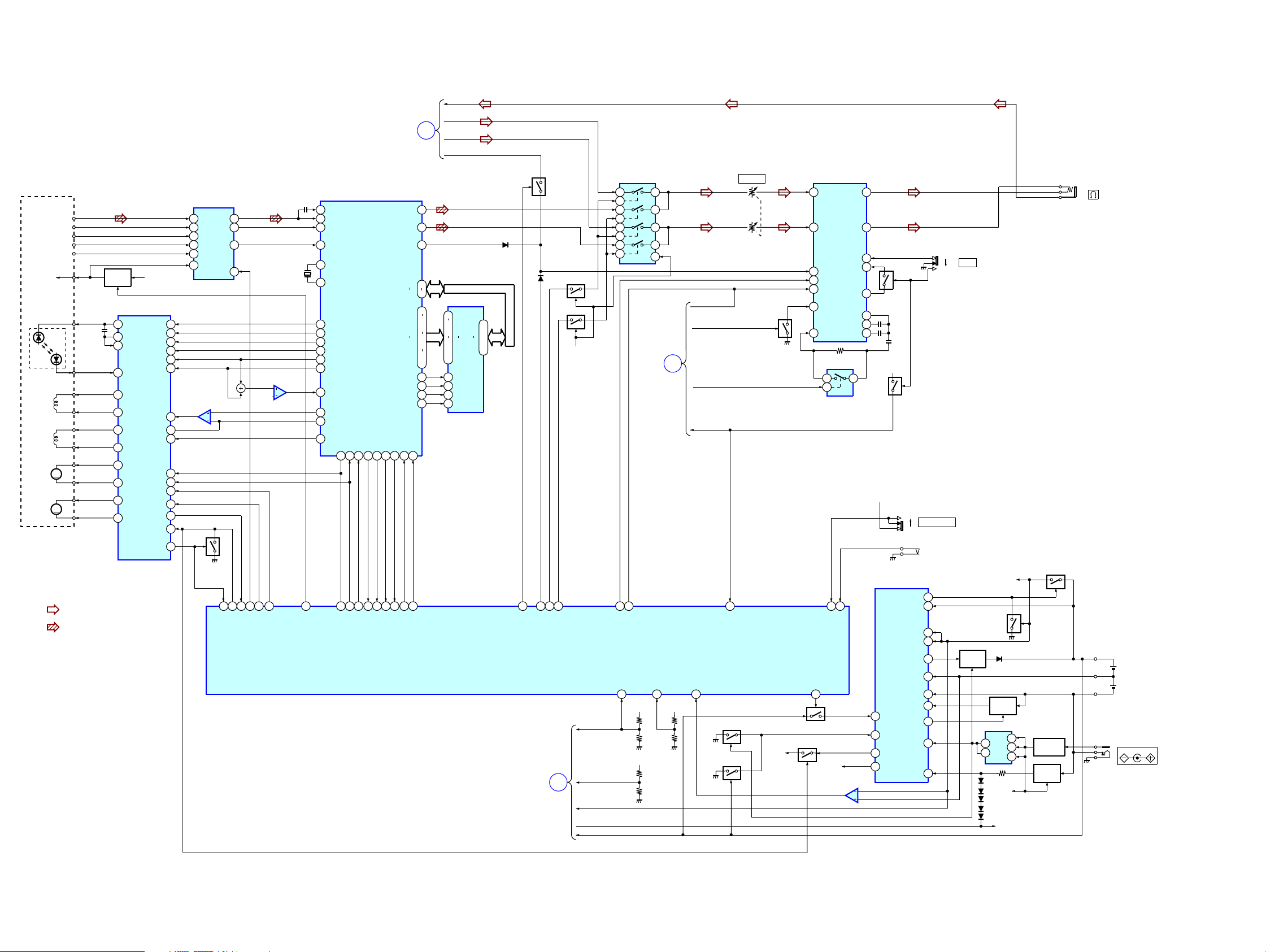
5-1. BLOCK DIAGRAMS
CD SECTION
OPTICAL PICK-UP
DAX-23E
VCC
LD
M
M
• Signal Path
: FM
: CD
RF
A
B
E
F
Q501
+B
SWITCH
IC401(1/2)
COIL/MOTOR
LD
PD
F+
F-
T+
T-
S+
S-
C+
C-
69
VLGO2
4
INM2
77
RF21
78
PAPC
36
FO2
34
RO2
32
FO3
30
RO3
40
FO1
38
RO1
28
FO4
26
RO4
DETECTOR
LASER
DIODE
PD
FOCUS
COIL
TRACKING
COIL
M901
SLED
MOTOR
M902
SPINDLE
MOTOR
DRIVE
VCC1 2V
DATA
CLOCK
CHGMNT
WAKEUP
RSTB
FM ANT
TUNER
SECTION
IC601
RF AMP,SERVO,DSP
71
RFAC
58
RFDC
62
A
59
E
93
XTAI
94
XTAO
46
SFDR
47
SRDR
50
FFDR
51
FRDR
48
TFDR
49
TRDR
29
ATSK
43
MDP
42
C176
44
MDS
D/A CONV,D-RAM CONT
SDTO23CLOCK
SENS
XLAT
25
24
26
12
10
43
11
25
SCK
XLAT
MSDTI
MSDTO
A MUTING
SCOR17FOK35R4M
30
3
79
XIN
FOK
SCOR
L OUT
R OUT
D0
D3
A0
A10
XWE
XOE
XCAS
XRAS
XSOE28XRST
44
XSOE9XRST
21
IC501
I-V AMP
RF RFO
IV2+
IN2+
IN2-
IV3+
IN3+
IN3-
STBY
GCNT
IC402
3
1
78
15
13
11
10
13
RESET
15
WAKEUP
AD CHGMNT
4
48
AGC PWM
IC604
3
46
XPOWLT
XAPC OFF
X601
16.9MHz
4
42
XHG ON
1
3
4
5
6
9
41FI1
42RI1
43FI2
RI2
44
FI3
12
RI3
13
FI4
RF2
4
14
7SYNC
15RI4
10
9
11LATCH
3
58
8
Q409
52
TU-L
A
TU-R
TUMUTE
RV301
Q601
97
104
2
D0D3A0
3
24
25
IC801(2/2)
D603
D601
Q306
Q305
.
.
.
56
SEG8
TUNER
SECTION
47
7
A MUTING
45
TU AUDIO
CD AUDIO
C
TUVCC+
AD I BATT
AD I HIDC
VCPU 2V
TUVCC+
VIN 3V
13
115
118
106
109
.
7
5
.
3
1
.
111
114
120
119
113
IC602
DRAM
9
12
.
15
A10
19
.
21
.
8
4
XWE
22
XOE
23
XCAS
5
XRAS
SYSTEM CONTROL
IC302
11 10
12
8
6
1
13
3
5
VCC
TUNER
SECTION
2
28
BEEP
HPSW
AD BATMNT
17
VIN 3V
VIN 3V
9
2
4
14
20
B
DCINMNT
4.5V
BEEP O HP
TU BASS1
TU BASS2
AVLS I SW
BATDET
41
VOLUME
Q304
38
AVLS
Q413,414
VCC1 2V
Q408,410
Q406,407
Q405
14
15
19
20
17
23
1
VCC2ON
8
VCC2 3.3V
HP AMP
L IN
R IN
MUTE
PWR SW
BEEP
BB SW
BST NF
2
4
36
IC301
MIX OUT
IC304
21
COMPON
WP OPEN
4
L OUT
R OUT
1
IC404
1
3
8
6
12ALC DET
11ALC IN
10
21BIAS
2AD DOUT
24BST OUT
VCPU 2V
Q301
VCPU 2V
Q302
IC401(2/2)
POWER CONTROL
71
L3
53
DTC2D
51
VCC1
72
VLG3
OFF
ON
STNG
V IN
BATM1
BATM2
CHG SW
DC IN
NORM
LIMIT
S802
G-PROTECTION
S801
(OPEN/CLOSE)
18
65
61LGO1
50VCPU
48RF4
60
59
RS
46
45
49
VG
5
S804
AVLS
Q402
CHARGE
SWITCH
7
8
D408
D301
D302
VCPU 2V
Q416
D401
Q403
CHARGE
ON/OFF
IC405
+4.8V
REG
+4.5V
TUVCC+
J302
Q411
DRY BATTRY
SIZE "AA"
(IEC DESIGNATION LR6)
2PCS 3V
1
Q412
3
+B SWITCH
4
Q404
SWITCH
J401
DC IN 4.5V
1010
Page 11
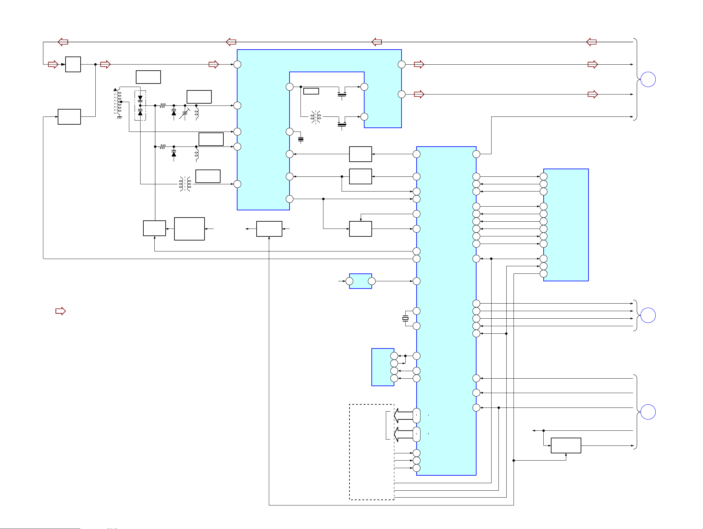
TUNER SECTION
D-FS18
FM ANT
FL1
B.P.F
Q3
FM
LOCAL/DX
L3
MW FERRITE-ROD
ANTTENA
D3
AM
TRACKING
Q84,85
LPF
TRACKING
CT1
L4
AM OSC
T81,Q86
DC/DC
CONVERTER
FM
FM RF
F-COVER
FM OSC
F-COVER
L1
L2
AM
FM
V IN
2
24
22
21
20
FM IN
FM RF
AM RF
FM OSC
AM OSC
MIX OUT
QUAD
LPF2
XAM/FM
XIF REQ
OSC OUT
Q4,5
+B SWITCH
IC1
FM /AM
IF/RF AMP
CF2,3
4
AM IF
T1
AM IFT
10
13
17
19
V INTU +B
X1
10.7MHz
10.7MHz
450kHz
V IN
CF1
3
7
6
Q2
AM/FM
SWITCH
Q6
IF ON
CONTROL
Q60
BUFFER
IC81
+1.6V
REG
FM IF
AM IF
2
L OUT
R OUT
12
11
IC61
DTS µCOM
59
61
64
71
60
70
65
55
45
AM/XFM
IF REQ
IF IN
AM IN
+B ON/OFF
FM IN
EQ
DX O CTR
AD DC REF
SDO O CDU
SDI I CDU
SCK I CDU
LCD REQ
CDON IWP CDU
LID OPEN
TUON
RESET
ACK CD
62TUMUTE
47
46
48
38
28
39
73
29
54
42AD1 KEY
IC801(1/2)
SYSTEM CONTROL
31
(CD)SDI
32
(CD)SDO
30
TUSCK
34
TUON
33
LCD REQ
5
CDON
29
XCD RESET TU
21
WP OPEN
19
ACK CD
18
AD CD KEY
39
HOLD
6
TU PWSWEN
TU-L
TU-R
TUMUTE
A
CD
SECTION
• Signal Path
: FM
IC62
EEPROM
DI
DO
SK
CS
SWITCH
UNIT
LCD
LOCAL DX
AM STEP SW
PRESETKEYS
CD/RADIO KEYS
VCPU
HOLD
X61
75kHz
3
4
2
1
75
XIN
74
XOUT
30
EEP DO/DI
31
EEP SK
32
EEP CS
1
COM0
4
COM3
5
S16
20
25
XLOCAL DET
21
AM STEP
36
MEM KEY
TU BEEP
49
TU BASS1
TU BASS2
XAVLS I SW
XHOLD I SW
AD2 BATT
AD3 HIDC
S1
VDD
58
56
52
51
43
44
72
V IN
Q8,9
+B SWITCH
BEEP O HP
TU BASS1
TU BASS2
AVLS I SW
AD I BATT
AD I HIDC
VCPU 2V
VIN 3V
TU VCC
B
C
CD
SECTION
CD
SECTION
1111
Page 12

D-FS18
5-2. PRINTED WIRING BOARD MAIN (SIDE A) SECTION
A
B
C
• Semiconductor
Location
Ref. No. Location
D403 I-5
D408 I-5
D461 E-6
D601 E-7
D
E
F
G
H
OPTICAL PICK-UP
BLOCK DAX-23E
IC405
IC402
IC404
IC304
IC304 F-3
IC402 E-4
IC404 E-5
IC405 E-10
Q301 G-3
Q403 D-10
Q405 F-4
Q406 H-5
Q407 I-5
Q409 I-5
Q412 E-10
Q413 G-4
Q501 D-3
I
J
12
34567891011
1212
Page 13

5-3. PRINTED WIRING BOARD MAIN (SIDE B) SECTION
A
IC62
B
D-FS18
C
D
E
F
G
H
IC81
IC1
IC61
• Semiconductor
Location
IC604
IC501
IC801
IC601
IC302
IC301
IC602
IC401
I
J
12
34567891011
Ref. No. Location
D1 C-7
D2 C-6
D3 C-8
D80 E-5
D82 E-5
D301 E-9
D302 E-9
D401 D-2
D404 E-3
D405 I-8
D602 F-7
D603 F-7
D804 E-5
IC1 B-6
IC61 C-4
IC62 B-3
IC81 B-3
IC301 F-9
IC302 E-9
IC401 H-8
IC501 D-10
IC601 E-7
IC602 G-6
IC604 D-9
IC801 E-4
Q2 C-6
Q3 B-7
Q4 D-5
Q5 D-5
Q6 B-6
Q8 C-5
Q9 C-5
Q60 C-5
Q84 C-5
Q85 C-4
Q86 F-6
Q302 I-8
Q304 E-10
Q305 E-10
Q306 E-9
Q402 D-2
Q404 F-4
Q408 I-7
Q410 I-8
Q411 G-7
Q414 F-9
Q416 I-9
Q601 D-6
1313
Page 14

D-FS18
5-4. SCHEMATIC DIAGRAM TUNER SECTION
IC B/D
1414
Page 15

5-5. SCHEMATIC DIAGRAM CD SECTION (1/4)
D-FS18
1515
Page 16

D-FS18
5-6. SCHEMATIC DIAGRAM CD SECTION (2/4)
IC B/D
1616
Page 17

5-7. SCHEMATIC DIAGRAM CD SECTION (3/4)
D-FS18
IC B/D
1717
Page 18

D-FS18
5-8. SCHEMATIC DIAGRAM CD SECTION (4/4)
IC B/D
1818
Page 19

5-9. IC PIN FUNCTION DESCRIPTION
• IC801 TMP88CM22R-SFMP1 (SYSTEM CONTROLLER)
D-FS18
Pin No.
1
2
3
4
5
6
7
8
9
10
11
12
13
14
15
16
17
18
19
20
21
22
23
24
25
26
27
28
29
30
31
32
33
34
35
36
37
38
39
40
41
42
43
44
45
46
47
48
49-64
65-68
Pin Name
VSS
HPSW
FOK I
AGCPWM O
CDON O
TU PWSWEN O
AMUTE O
VCC2ON O
XRST O
SCK O
SCK O
MSDTO O
WAKEUP O
AD CDTEST
AD CHGMNT
RESERVE
AD BATMNT
AD CDKEY
ACK CD I
AD DCINMNT
WP OPEN
VREFL
VREFH
VDD
SCOR I
GRSCOR I
MIR I
BEEP O
XCDRESET TU O
TUSCK O
SDI I
SDO O
LCDREQ
TUON I
CD RW I
COMPON I
DIG TU I
AVLS I
HOLD I
EXBATT I
BATDET
XHGON O
XLAT O
XSOE O
CDAUDIO O
XPOWLT O
TUAUDIO O
XAPC OFF O
SEG15-SEG0
COM3-COM0
I/O
—
Ground terminal.
—
Headphone IC power switch.
I
Focus OK signal input from the digital servo processor (IC601). “L”:NG,”H”:OK
O
AGC control puls signal output terminal.
O
CD mode on.
O
tuner power block on.(Supply vin)
O
Analog audio muting ON/OFF control signal output terminal. “H”:muting ON
O
VCC2 voltage control signal output terminal.
O
Reset signal output to IC601. “L”:reset
O
Serial data transfer clock signal output to IC601.
I
Serial data input from the IC601.
O
Serial data output to IC601.
O
WAKE-UP control signal output terminal. (for system standby reset)
I
Plug-in detection signal input terminal of LINE OUT/OPTICAL OUT.
I
Batery charge voltage detection input from the power control(IC401).
I
Not used.
I
Batery voltage monitor signal input .
I
Main switch unit kye AD port.
I
Acknowledgement and status from DTS.
I
DC in voltage monitor signal input.
I
Upper lid ststus signal input.
I
Analog GND for A/D signal input.
I
Analog VDD for A/D signal input.
—
Power supply terminal(+2V).
I
Sub-code sync(S0+S1)detection signal input from the IC601.
I
GRSCOR signal input from the IC601.
I
H-MIRX series, L-MISX
O
Beep sound output to the headphone amplifier(IC302).
O
DTS pull up 200K.
O
Communication clock output to the communication format converter (IC802).
I
Serial data out to DTS.
O
Serial data in to DTS.
O
LCD buty data send request signal output.
O
Radio mode status signal output.
I
H-CD RW disc enabled , L-disabled.
I
ADPCM compression on sigunal inout.
I
Not used.
I
Automatic volume limit system.
I
HOLD switch detection signal input.
I
Not usde.
O
Signal cell battery detection sigunal output.
O
Optical pick-up power ON/OFF control signal output terminal. “L”:ON.
O
Serial data latch pulse signal output to IC601.
O
Serial data output enable signal output terminal.
O
Audio channel selection. (Raidio/CD music)
O
Latch signal output to the power control(IC401).
O
Audio channel selection. (Raidio/CD music)
O
APC mute signal output terminal. “L”:mute
O
LCD segment signal output.
O
Not usde.
Description
19
Page 20

D-FS18
Pin No.
69-71
72,73
74
75
76
77
78
79
80
Pin Name
V3-V1
C1,C0
STOP
ICTEST
NC
NC
RESET I
XIN I
XOUT
I/O
O
Not usde.
O
Not usde.
O
Auto.
I
Test terminal for IC (Fixed at “L”).
O
Not usde.
O
Not usde.
I
System reset signal input from the power control(IC401). “L”:reset.
I
System clock input terminal.
—
Not usde.
Description
20
Page 21

• IC61 TC9327AF-630 (DTSµCOM)
Pin No.
1 to 4
5 to 20
21
22
23
24
25
26
27
28
29
30
31
32
33
34
35
36
37
38
39
40
41
42
43
44
45
46
47
48
49
50
51
52
53
54
55
56
57
58
59
Pin Name
COM1-4
S1-16
AMSTEP-I
DEST2-I
DEST1-I
DEST0-I
XLOCAL/XMONO-DET_I
NC
NC
LCDREQ-I
LID OPEN
EEPSD
EEPSK
EEPCS
XL/O-I
NC
NC
PRESET_KEY
NC
CD_ACK-I
CDON-I
NC
NC
KEY
RMKEY
HIDC_BATT
ADREF
TUCDSDI
TUCDSDO
TUCDSCK
TUBEEP
NC
XHOLD
XAVLS
XDC IN DET
TUON
ST-DX
TUBASS2
TUTEST
TUBASS1
AM/XFM-O
I/O
O
LCD drivers
O
LCD drivers
I
AM 9K/10K tuning step select (initialisation)
I
Bit 2 Tu Destination setting
I
Bit 1 Tu Destination setting
I
Bit 0 Tu Destination setting
I
Local/DX or Mono/Stereo ON-Off switch detection
O
Not used
O
Not used
I
LCD display request signal from CD
I
Upper Lid Open Detect
I/O
Data I/O for EEPROM
O
Clock for EEPROM 2K bits (software timing)
O
Chip select for EEPROM
I
Line Out Jack detect
—
Not used
—
Not used
I
Memory key ( use Vdd as ref) 5 keys
I
Not used
O
TU On request
I
CD ON request (Weakup TU in sleep mode)
—
Reserved
—
Not used
I
Set Keys
I
Remote Key
I
Battery/ HiDC Level detect (use VEE1.55 or 3.3V external)
I
Ref DC of A/D (use for HiDC and batt detects, keys ,vol +,- and RMkeys use VDD as ref)
I
Serial input from CD micon
O
Serial output to CD micon (reserved line) Not use
I
Serial clock to CD micon
O
Beep sound control
—
Not used
I
HOLD detect
I
AVLS detect
I
DC-in detect
O
Acknowlege CD
O
Local/DX or Mono/Stereo ON-Off control
O
Sound mode, Mega Bass 2
I
TU Test Mode detect (active LOW)
O
Sound mode, Mega Bass 1
O
Band control FM/AM to Tuner IC TA2104
Description
D-FS18
21
Page 22

D-FS18
Pin No.
60
61
62
63
64
65
66
67
68
69
70
71
72
73
74
75
76
77
78
79
80
Pin Name
+B ON/OFF
IFREQ-O
TUMUTE-O
TEST
IFIN
EO
NC
HOLD
NC
GND
FMIN
AMIN
VDD
RESET
XOUT
XIN
VXT
VLCD
C1
C2
VEE
I/O
O
Radio Power On/Off (VCO Amp block)
O
IF Request
O
Mute HP control
—
Not used
I
FM,AM IF input
O
PLL error output
—
Not used
I
Not used
O
Not used
—
IC System GND
I
FM OSC in
I
AM OSC in
—
VDD power supply 3.0V
I
Power reset (Resset by CD Micon)
—
Crystal Osc pin
—
Crystal Osc pin
—
Crystal Osc pin
—
LCD voltage doubler
—
LCD voltage doubler
—
LCD voltage doubler
—
Constant voltage for LCD 1.55V
Description
22
Page 23

5-10. IC BLOCK DIAGRAMS
IC1 TA2104BFN
D-FS18
FM RF OUT
RF VCC AM RF IN FM OSC AM OSC OSC OUT ST LED IF REQ DET OUT LPF1 LPF2
24 23 22 21 20 19 18 17 16 15 14 13
SW
IF
REQ
IF
AM
DET
AF
BUFF
AGC
FM
DET
AF
VCO
DIVIDE
ST/MO
FM/AM
AM
OSC
FM
OSC
BUFF
BUFF
AM
MIX
FM
RF
FM
MIX
LEVEL
AMIF
DET
ST
BUFF
1/8
FMIF
1110987654321 12
RF GND FM RF IN AM IF IN FM IF IN GND AGC QUAD R-OUT L-OUTAM LOW
MIX OUT VCC
CUT
DECODE
MUTE
IC301 TA2120FN
BST
BST
SW
OUT
24
23
ADD
B
BST
+
–
2
1
BSTNFADD
OUT
ADD
A
BIAS
BIAS
IN
21
22
BIAS
PWC
SW
3
RF IN PWC
SW
4 5
PW
SW
SW
20 19 18
PWSWMT
SW
+
–
PW
B
6
VCC
OUT B OUT C OUT A PWR
TC
OUT B
PW
C
7
BEEP
BEEP
+
MT
MT
ATT
IN AIN BGND
IN
17
OUT A
–
PW
A
8
GND
16
9
15
ALC ALC
10
MIX
OUT
14
ALC
DET
11
ALCINALC
DET
SW
13
ATT
SW
12
23
Page 24

D-FS18
IC401 TB2119FA
BATM1
BATM2
CHGMNT
INP1
RF1
INM1
DTC1D
DTC2D
RSTB
VCC1
VCPU
DCIN
RF4
INM4
CHGSW
RI2
4142434445464748495051525354555657585960
RS
FI1
RI1
FI2
VLGO1
L1L
PGND1
L1H
VIN
L2H
PGND2
L2L
VLGO2
PGND3
VLG3
INP3
INM3
RF3
DTC3
FO1
61
62
63
64
65
66
67
68
69
70
71
L3
72
73
74
75
76
STNBY
REFERENCE
BANDGAP
REFERENCE
(VREF)
BIAS
SAW GEN
CLK
OR OSC
CONTROLLER
CONTROL
CHARGE
LEVEL
SHIFTER
LEVEL
SHIFTER
H BRIDGE
DRIVER1
H BRIDGE
DRIVER2
H BRIDGE
DRIVER3
H BRIDGE
DRIVER4
40
39
38
37
36
35
34
33
32
31
30
29
28
27
26
25
MGND1
RO1
VD12
FO2
MGND2
RO2
VD23
FO3
MGND3
RO3
VD34
FO4
MGND4
RO4
HPOUT1
RF21
PAPC
APCREF
VINDET
77
78
79
80
1 2 3 4 5 6 7 8 16 17 18 19 20
VREF
L4
RF2
INM2
VG
GND
SYNC
WAKE UP
CLOCK
DATA
LATCH
INTERFACE
FI3
RI3
1514131211109
PWM4
FR4
CONTROLLER
HPI1
HPI2
STNG
DRIVER
N.C.
PWM
H/P
HIPC
24
23
22
21
HCND
HPOUT3
VHP
HPOUT2
24
Page 25

IC601 CXD3028R
XOE
XCASD2D3D0D1
120 119 118 117 116 115 114 113 112 111 110 109 108 107 106 105 104 103 102 101 100 99 98 97 96 95 94 93 92 91
D2D3D0
XOE
XCAS
XWE
XRAS
A11
A10
DVDDA0A1A2A3
A11
A10
DVDD
A0A1A2
D1
XWE
XRAS
AVDD2
LOUT2
AIN2
AOUT2
AVSS2
AVSS1
AOUT1
AIN1
LOUT1
AVDD1
XVSS
XTAO
XTAI
XVDD
A3
LOUT2
AVDD2
AIN2
AOUT2
AVSS2
AVSS1
AOUT1
AIN1
LOUT1
XVSS
AVDD1
XTAO
XTAI
XVDD
D-FS18
BCKI
BCKI
DVSS
A5/PWMI
XWRE
XRDE
XEMP
XWIH
XQOK
AMUTE
SDTI
XQCK
SCSY
SCOR
VSS0
SBSO
EXCK
XRST
SYSM
SDTO
XLAT
CLOK
SENS
SCLK
XSOE
ATSK
R4M
VPCO
WFCK
DEMODULATOR
CONVERTER
GFS
MDS
XUGF
EFM
SUB CODE
PROCESSOR
SERVO
AUTO
SEQUENCER
A/D
ERROR
CORRECTOR
32K
RAM
PROCESSOR
C2PO
D/A
INTERFACE
SIGNAL
BLOCK
SERVO
INTERFACE
MIRR
DFCT
FOK
SERVO DSP
FOCUS SERVO
TRACKING
SERVO
SLED SERVO
WDCK
VIBRATION
MEMORY
CONTROLLER
COMPRESSION
EXPANDER
DAC
MEMORY CONTROLLER,
BUS BOOST BLOCK
LPF
LPF
PWM GENERATOR
FOCUS PWM
GENERATOR
TRACKING PWM
GENERATOR
GENERATOR
+
SLED PWM
SELECTOR
DIGITAL
OUT
XOE
XCAS
XWE
XRAS
XQOK
XWIH
XEMP
XRDE
XWRE
D0 – D4
A0 – A11
SYSM
AMUTE
HPL
HPM
HPR
PCMDI
LRCKI
BCKI
AOUT1
AIN1
LOUT1
LOUT2
AIN2
AOUT2
ATSK
SCLK
SSTP
COUT
DFCT
MIRR
SRDR
FOK
FRDR
FFDR
TRDR
TFDR
SFDR
BCK
PCMD
LRCK
DOUT
BCK
PCMDI
PCMD
LRCKI
LRCK
DOUT
VDD2
WFCK
C2PO
GFS
XPCK
XUGF
WDCK
VSS2
XTSL
AVDD3
ASYO
ASYI
BIAS
RFAC
AVSS3
CLTV
PCO
FILI
FILO
VCTL
VPCO
VC
A
B
90
BCK
89
PCMDI
88
PCMD
87
LRCKI
86
LRCK
85
DOUT
84
VDD2
83
WFCK
82
C2PO
81
GFS
80
XPCK
79
XUGF
78
WDCK
77
VSS2
76
XTSL
75
AVDD3
74
ASYO
73
ASYI
72
BIAS
71
RFAC
70
AVSS3
69
CLTV
68
PCO
67
FILI
66
FILO
65
VCTL
64
VPCO
63
VC
62
A
61
B
XTAI
XTSL
VCTL
XTAO
CLOCK
GENERATOR
RFAC
BIAS
ASYMMETRY
ASYI
CORRECTOR
ASYO
FILO
FILI
DIGITAL
PCO
SDTI
R4M
E
F
B
A
VC
D GND
PLL
DIGITAL
CLV
CPU
INTERFACE
SERVO BLOCK
OP AMP
ANALOG SWITCH
CLTV
XPCK
A9
1
A9
A8
2
A8
A7
3
A7
DVSS
4
A6
5
A6
A5
6
A4
7
A4
XWRE
8
XRDE
9
XEMP
10
XWIH
11
XQOK
12
AMUTE
13
SDTI
14
15
SCSY
16
SCOR
17
VSS0
18
SBSO
19
EXCK
20
21
SYSM
22
SDTO
23
XLAT
24
CLOK
25
SENS
26
SCLK
27
XSOE
28
ATSK
29
R4M
30
PWMI
LOCK
MDP
SCSY
SCOR
SBSO
EXCK
SDTO
XLAT
CLOK
SENS
XSOE
IGEN
RFDC
D VDD
FOK
DFCT
VDD0
COUT
MIRR
PWMI
31 32 33 34 35 36 37 38 39 40 41 42 43 44 45 46 47 48 49 50 51 52 53 54 55 56 57 58 59 60
FOK
DFCT
VDD0
COUT
MIRR
HPR
HPM
LOCK
HPR
HPM
LOCK/HPL
PWMI/HPVSS
HPL
VDD1
VDD1
HPL/HPVDD
C176
MDP
MDP
MDS
MDS
SSTP
SSTP
SFDR
SFDR
SRDR
SRDR
TFDR
TFDR
TRDR
TRDR
FFDR
FFDR
FRDR
FRDR
VSS1
VSS1
TEST
TES1
A VDD
AVDD0
AVDD0
IGEN
IGEN
A GND
AVSS0
AVSS0
RFDC
RFDC
E
E
F
F
25
Page 26

D-FS18
Ver. 1.1
NOTE:
• -XX, -X mean standardized parts, so they may
have some differences from the original one.
• Items marked “*” are not stocked since they
are seldom required for routine service. Some
delay should be anticipated when ordering these
items.
6-1. CABINET SECTION
SECTION 6
EXPLODED VIEWS
• The mechanical parts with no reference number
in the exploded views are not supplied.
• Hardware (# mark) list and accessories and
packing materials are given in the last of this
parts list.
The components identified by mark 0 or
dotted line with mark 0 are critical for safety.
Replace only with part number specified.
Les composants identifiés par une marque
0 sont critiques pour la sécurité.
Ne les remplacer que par une pièce portant
le numéro spécifié.
29
32
8
10
9
11
10
13
12
a
b
b
a
33
14
a
31
15
29
14
17
7
16
30
6
23
18
22
21
a
14
CDM-3123EBA
13
19
20
4
21
5
3
24
2
25
26
1
27
28
1
Ref. No. Part No. Description Remarks Ref. No. Part No. Description Remarks
1 4-908-792-51 SCREW (B2)
2 X-3380-333-1 BUCKLE SUB ASSY
3 X-3380-572-1 BRACKET (ROLLER) ASSY
4 3-338-687-21 SCREW (M1.4X2), TAPPING
5 3-343-254-41 SCREW (B1.7X3.5), TAPPING
6 3-225-157-01 COVER, LID
7 1-476-429-11 SWITCH UNIT
8 3-221-301-01 PACKING (UPPER LID)
9 3-224-858-01 SPACER
10 3-224-719-01 SPACER (C)
11 3-225-462-01 SPACER (D)
12 X-3379-446-1 CABINET (INNER) ASSY
13 4-908-792-71 SCREW (B2)
14 4-222-765-01 INSULATOR
15 3-047-194-01 SHEET (CDM), ADHESIVE
18 3-318-201-51 SCREW (B) (1.4X4), TAPPING
19 X-3379-391-1 ARM ASSY, SWITCHING
20 3-387-566-01 SCREW, STEP
21 3-326-536-11 SCREW, TAPPING
22 3-221-310-01 LEVER (VOL) (B)
23 3-221-311-01 PACKING (H/P)
24 3-225-155-01 CABINET (LOWER)
25 3-221-312-01 PACKING (DC-IN)
26 3-225-154-01 BRACKET (STRAP)
27 3-221-329-01 RING, O
28 3-221-321-01 KNOB (VOL)
29 X-3380-729-1 LID ASSY, UPPER
29 3-221-318-01 LEVER, DETECTION
30 3-229-056-01 LEAF, COPPER
31 3-318-201-31 SCREW (B) (1.4X5), TAPPING
* 16 A-3323-695-A MAIN PC BOARD ASSY
17 4-223-609-01 KNOB (JOGGABLE)
26
32 3-375-114-71 SCREW
33 X-3380-356-1 LID BATTERY CASE ASSY
Page 27

6-2. MECHANISM SECTION
(CDM-3123EBA)
D-FS18
51
M902
53
52
63
61
62
60
59
58
54
55
M901
not supplied
57
56
51
Ref. No. Part No. Description Remarks Ref. No. Part No. Description Remarks
51 3-318-203-71 SCREW(B1.7X5),TAPPING
52 4-218-820-01 CHASSIS
53 A-3328-628-A SCREW(FEED)ASSY
54 4-218-823-01 GEAR(B)
55 4-964-564-01 SCREW(M1.2X1.6)
56 4-218-821-01 COVER,GEAR
57 4-218-825-01 SPPRING(SLED)
58 3-895-823-31 SCREW(B1.4X2.3),TAPPING
59 4-220-645-01 SHAFT,STANDARD
60 4-223-600-01 RACK
61 4-218-827-01 BRACKET(SHAFT)
62 3-686-458-03 SCREW(P1.4X3.5),TAPPING
063 X-4952-506-1 OPTICAL PICK-UP(DAX-23E)
M901 A-3328-627-A MOTOR ASSY,SLED(WITH GEAR)
M902 A-3328-759-A MOTOR ASSY,TURN TABLE(SPINDLE)
The components identified by
mark 0 or dotted line with mark
0 are critical for safety.
Replace only with part number
specified.
Les composants identifiés par
une marque 0 sont critiques
pour la sécurité.
Ne les remplacer que par une
pièce portant le numéro spécifié.
27
Page 28

D-FS18
SECTION 7
MAIN
NOTE:
• Due to standardization, replacements in the
parts list may be different from the parts
specified in the diagrams or the components
used on the set.
• -XX, -X mean standardized parts, so they
may have some difference from the original
one.
• Items marked “*” are not stocked since they
are seldom required for routine service.
Some delay should be anticipated when
ordering these items.
Ref. No. Part No. Description Remarks Ref. No. Part No. Description Remarks
* A-3323-695-A MAIN BOARD, COMPLETE
*********************
ELECTRICAL PARTS LIST
• CAPACITORS:
uF: µF
• RESISTORS
All resistors are in ohms.
METAL: metal-film resistor
METAL OXIDE: Metal Oxide-film resistor
F: nonflammable
• COILS
uH: µH
When indicating parts by reference number,
please include the board name.
C54 1-115-156-11 CERAMIC CHIP 1uF 10V
C58 1-162-970-11 CERAMIC CHIP 0.01uF 10% 25V
• SEMICONDUCTORS
In each case, u: µ, for example:
uA...: µA... , uPA... , µPA... ,
uPB... , µPB... , uPC... , µPC... ,
uPD..., µPD...
The components identified by mark 0 or
dotted line with mark 0 are critical for safety.
Replace only with part number specified.
Les composants identifiés par une marque
0 sont critiques pour la sécurité.
Ne les remplacer que par une pièce portant
le numéro spécifié.
3-221-307-01 TERMINAL BOARD (-), BATTERY
3-221-308-01 TERMINAL BOARD (RELAY),BATTERY
3-221-309-01 LEVER (VOL) (A)
4-223-413-01 SCREW (M1.4X3)
4-223-585-01 TERMINAL BOARD (+), BATTERY
< CAPACITOR >
C2 1-162-917-11 CERAMIC CHIP 15PF 5% 50V
C4 1-164-118-11 CERAMIC CHIP 15PF 5.00% 50V
C5 1-162-923-11 CERAMIC CHIP 47PF 5% 50V
C6 1-164-217-11 CERAMIC CHIP 150PF 5.00% 50V
C9 1-162-964-11 CERAMIC CHIP 0.001uF 10% 50V
C10 1-162-959-11 CERAMIC CHIP 330PF 5% 50V
C11 1-162-967-11 CERAMIC CHIP 0.0033uF 10% 50V
C12 1-162-927-11 CERAMIC CHIP 100PF 5% 50V
C13 1-164-227-11 CERAMIC CHIP 0.022uF 10% 25V
C15 1-162-923-11 CERAMIC CHIP 47PF 5% 50V
C16 1-162-970-11 CERAMIC CHIP 0.01uF 10% 25V
C17 1-164-346-11 CERAMIC CHIP 1uF 16V
C18 1-162-964-11 CERAMIC CHIP 0.001uF 10% 50V
C19 1-107-826-11 CERAMIC CHIP 0.1uF 10.00% 16V
C20 1-109-982-11 CERAMIC CHIP 1uF 10.00% 10V
C21 1-164-156-11 CERAMIC CHIP 0.1uF 25V
C22 1-164-315-11 CERAMIC CHIP 470PF 5.00% 50V
C23 1-164-315-11 CERAMIC CHIP 470PF 5.00% 50V
C24 1-162-970-11 CERAMIC CHIP 0.01uF 10% 25V
C25 1-117-887-11 TANTAL. CHIP 220uF 20.00% 6.3V
C26 1-115-467-11 CERAMIC CHIP 0.22uF 10.00% 10V
C27 1-135-151-21 TANTALUM CHIP 4.7uF 20% 4V
C28 1-164-245-11 CERAMIC CHIP 0.015uF 10.00% 25V
C29 1-164-245-11 CERAMIC CHIP 0.015uF 10.00% 25V
C30 1-125-837-11 CERAMIC CHIP 1uF 10% 6.3V
C31 1-125-837-11 CERAMIC CHIP 1uF 10% 6.3V
C32 1-164-362-11 CERAMIC CHIP 470PF 5.00% 50V
C33 1-162-970-11 CERAMIC CHIP 0.01uF 10% 25V
C34 1-162-953-11 CERAMIC CHIP 100PF 5% 50V
C35 1-104-852-11 TANTAL. CHIP 22uF 20.00% 6.3V
C36 1-162-970-11 CERAMIC CHIP 0.01uF 10% 25V
C39 1-162-970-11 CERAMIC CHIP 0.01uF 10% 25V
C40 1-162-970-11 CERAMIC CHIP 0.01uF 10% 25V
C41 1-162-927-11 CERAMIC CHIP 100PF 5% 50V
C45 1-162-970-11 CERAMIC CHIP 0.01uF 10% 25V
C46 1-162-964-11 CERAMIC CHIP 0.001uF 10% 50V
C50 1-162-966-11 CERAMIC CHIP 0.0022uF 10% 50V
C51 1-162-966-11 CERAMIC CHIP 0.0022uF 10% 50V
C59 1-162-970-11 CERAMIC CHIP 0.01uF 10% 25V
C60 1-162-964-11 CERAMIC CHIP 0.001uF 10% 50V
C61 1-162-927-11 CERAMIC CHIP 100PF 5% 50V
C62 1-162-964-11 CERAMIC CHIP 0.001uF 10% 50V
C63 1-162-919-11 CERAMIC CHIP 22PF 5% 50V
C64 1-162-917-11 CERAMIC CHIP 15PF 5% 50V
C65 1-107-823-11 CERAMIC CHIP 0.47uF 10.00% 16V
C66 1-107-826-11 CERAMIC CHIP 0.1uF 10.00% 16V
C67 1-107-826-11 CERAMIC CHIP 0.1uF 10.00% 16V
C68 1-107-823-11 CERAMIC CHIP 0.47uF 10.00% 16V
C69 1-104-852-11 TANTAL. CHIP 22uF 20.00% 6.3V
C70 1-162-964-11 CERAMIC CHIP 0.001uF 10% 50V
C72 1-107-826-11 CERAMIC CHIP 0.1uF 10.00% 16V
C76 1-162-970-11 CERAMIC CHIP 0.01uF 10% 25V
C80 1-162-970-11 CERAMIC CHIP 0.01uF 10% 25V
C81 1-162-964-11 CERAMIC CHIP 0.001uF 10% 50V
C82 1-164-489-11 CERAMIC CHIP 0.22uF 10.00% 16V
C83 1-162-927-11 CERAMIC CHIP 100PF 5% 50V
C84 1-162-970-11 CERAMIC CHIP 0.01uF 10% 25V
C85 1-164-505-11 CERAMIC CHIP 2.2uF 16V
C86 1-162-915-11 CERAMIC CHIP 10PF 0.5PF 50V
C87 1-162-915-11 CERAMIC CHIP 10PF 0.5PF 50V
C88 1-162-970-11 CERAMIC CHIP 0.01uF 10% 25V
C90 1-104-852-11 TANTAL. CHIP 22uF 20.00% 6.3V
C92 1-162-970-11 CERAMIC CHIP 0.01uF 10% 25V
C93 1-162-964-11 CERAMIC CHIP 0.001uF 10% 50V
C94 1-164-156-11 CERAMIC CHIP 0.1uF 25V
C97 1-107-826-11 CERAMIC CHIP 0.1uF 10.00% 16V
C98 1-164-505-11 CERAMIC CHIP 2.2uF 16V
C102 1-162-962-11 CERAMIC CHIP 470PF 10% 50V
C104 1-164-936-11 CERAMIC CHIP 680PF 10.00% 16V
C121 1-115-156-11 CERAMIC CHIP 1uF 10V
C123 1-162-927-11 CERAMIC CHIP 100PF 5% 50V
C124 1-107-826-11 CERAMIC CHIP 0.1uF 10.00% 16V
C202 1-164-935-11 CERAMIC CHIP 470PF 10.00% 16V
C204 1-162-963-11 CERAMIC CHIP 680PF 10% 50V
C221 1-115-156-11 CERAMIC CHIP 1uF 10V
C223 1-162-927-11 CERAMIC CHIP 100PF 5% 50V
C224 1-107-826-11 CERAMIC CHIP 0.1uF 10.00% 16V
C321 1-164-156-11 CERAMIC CHIP 0.1uF 25V
C322 1-164-156-11 CERAMIC CHIP 0.1uF 25V
C323 1-115-156-11 CERAMIC CHIP 1uF 10V
C324 1-125-838-11 CERAMIC CHIP 2.2uF 10% 6.3V
C325 1-117-720-11 CERAMIC CHIP 4.7uF 10V
C326 1-117-720-11 CERAMIC CHIP 4.7uF 10V
28
Page 29

D-FS18
MAIN
Ref. No. Part No. Description Remarks Ref. No. Part No. Description Remarks
C327 1-115-156-11 CERAMIC CHIP 1uF 10V
C328 1-165-128-11 CERAMIC CHIP 0.22uF 16V
C329 1-164-505-11 CERAMIC CHIP 2.2uF 16V
C331 1-128-057-11 ELECT 330uF 20.00% 6.3V
C332 1-164-156-11 CERAMIC CHIP 0.1uF 25V
C333 1-115-156-11 CERAMIC CHIP 1uF 10V
C334 1-124-584-00 ELECT 100uF 20% 10V
C335 1-164-156-11 CERAMIC CHIP 0.1uF 25V
C401 1-162-970-11 CERAMIC CHIP 0.01uF 10% 25V
C402 1-135-259-11 TANTAL. CHIP 10uF 20.00% 6.3V
C403 1-164-941-11 CERAMIC CHIP 0.0047uF 10.00% 16V
C404 1-104-913-11 TANTAL. CHIP 10uF 20.00% 16V
C405 1-115-467-11 CERAMIC CHIP 0.22uF 10.00% 10V
C406 1-124-584-00 ELECT 100uF 20% 10V
C407 1-162-970-11 CERAMIC CHIP 0.01uF 10% 25V
C408 1-162-925-11 CERAMIC CHIP 68PF 5.00% 50V
C409 1-124-584-00 ELECT 100uF 20% 10V
C410 1-124-584-00 ELECT 100uF 20% 10V
C411 1-125-837-91 CERAMIC CHIP 1uF 10% 6.3V
C412 1-164-156-11 CERAMIC CHIP 0.1uF 25V
C413 1-164-937-11 CERAMIC CHIP 0.001uF 10.00% 16V
C414 1-162-966-11 CERAMIC CHIP 0.0022uF 10% 50V
C415 1-164-156-11 CERAMIC CHIP 0.1uF 25V
C417 1-104-752-11 TANTAL. CHIP 33uF 20.00% 6.3V
C418 1-124-635-00 ELECT 220uF 20.00% 6.3V
C420 1-110-569-11 TANTAL. CHIP 47uF 20.00% 4V
C421 1-135-201-11 TANTALUM CHIP 10uF 20% 4V
C422 1-109-982-11 CERAMIC CHIP 1uF 10.00% 10V
C423 1-164-943-11 CERAMIC CHIP 0.01uF 10.00% 16V
C424 1-164-677-11 CERAMIC CHIP 0.033uF 10.00% 16V
C425 1-115-156-11 CERAMIC CHIP 1uF 10V
C426 1-109-982-11 CERAMIC CHIP 1uF 10.00% 10V
C427 1-115-467-11 CERAMIC CHIP 0.22uF 10.00% 10V
C428 1-164-230-11 CERAMIC CHIP 220PF 5.00% 50V
C429 1-117-720-11 CERAMIC CHIP 4.7uF 10V
C431 1-124-229-00 ELECT 33uF 20% 10V
C432 1-117-720-11 CERAMIC CHIP 4.7uF 10V
C433 1-164-941-11 CERAMIC CHIP 0.0047uF 10.00% 16V
C435 1-117-720-11 CERAMIC CHIP 4.7uF 10V
C436 1-115-467-11 CERAMIC CHIP 0.22uF 10.00% 10V
C437 1-125-891-11 CERAMIC CHIP 0.47uF 10.00% 10V
C439 1-124-635-00 ELECT 220uF 20.00% 6.3V
C440 1-115-467-11 CERAMIC CHIP 0.22uF 10.00% 10V
C442 1-115-156-11 CERAMIC CHIP 1uF 10V
C443 1-115-156-11 CERAMIC CHIP 1uF 10V
C444 1-124-584-00 ELECT 100uF 20% 10V
C446 1-104-913-11 TANTAL. CHIP 10uF 20.00% 16V
C451 1-164-346-11 CERAMIC CHIP 1uF 16V
C453 1-115-467-11 CERAMIC CHIP 0.22uF 10.00% 10V
C461 1-107-823-11 CERAMIC CHIP 0.47uF 10.00% 16V
C462 1-162-925-11 CERAMIC CHIP 68PF 5.00% 50V
C501 1-164-156-11 CERAMIC CHIP 0.1uF 25V
C502 1-117-720-11 CERAMIC CHIP 4.7uF 10V
C504 1-125-838-11 CERAMIC CHIP 2.2uF 10% 6.3V
C505 1-115-156-11 CERAMIC CHIP 1uF 10V
C508 1-125-838-11 CERAMIC CHIP 2.2uF 10% 6.3V
C602 1-115-467-11 CERAMIC CHIP 0.22uF 10.00% 10V
C603 1-107-826-11 CERAMIC CHIP 0.1uF 10.00% 16V
C604 1-162-968-11 CERAMIC CHIP 0.0047uF 10% 50V
C605 1-164-156-11 CERAMIC CHIP 0.1uF 25V
C606 1-164-874-11 CERAMIC CHIP 100PF 5.00% 16V
C607 1-125-891-11 CERAMIC CHIP 0.47uF 10.00% 10V
C609 1-162-966-11 CERAMIC CHIP 0.0022uF 10% 50V
C611 1-162-917-11 CERAMIC CHIP 15PF 5% 50V
C612 1-162-967-11 CERAMIC CHIP 0.0033uF 10% 50V
C620 1-164-943-11 CERAMIC CHIP 0.01uF 10.00% 16V
C621 1-164-217-11 CERAMIC CHIP 150PF 5.00% 50V
C622 1-107-820-11 CERAMIC CHIP 0.1uF 16V
C623 1-115-156-11 CERAMIC CHIP 1uF 10V
C624 1-162-964-11 CERAMIC CHIP 0.001uF 10% 50V
C625 1-135-201-11 TANTALUM CHIP 10uF 20% 4V
C626 1-135-201-11 TANTALUM CHIP 10uF 20% 4V
C627 1-107-820-11 CERAMIC CHIP 0.1uF 16V
C628 1-164-156-11 CERAMIC CHIP 0.1uF 25V
C629 1-164-505-11 CERAMIC CHIP 2.2uF 16V
C630 1-162-915-11 CERAMIC CHIP 10PF 0.5PF 50V
C631 1-162-915-11 CERAMIC CHIP 10PF 0.5PF 50V
C632 1-115-156-11 CERAMIC CHIP 1uF 10V
C634 1-127-569-11 TANTAL. CHIP 100uF 20% 4V
C635 1-115-156-11 CERAMIC CHIP 1uF 10V
C636 1-164-156-11 CERAMIC CHIP 0.1uF 25V
C638 1-104-847-11 TANTAL. CHIP 22uF 20.00% 4V
C641 1-162-927-11 CERAMIC CHIP 100PF 5% 50V
C642 1-162-927-11 CERAMIC CHIP 100PF 5% 50V
C645 1-164-677-11 CERAMIC CHIP 0.033uF 10.00% 16V
C647 1-164-156-11 CERAMIC CHIP 0.1uF 25V
C803 1-107-820-11 CERAMIC CHIP 0.1uF 16V
C804 1-113-619-11 CERAMIC CHIP 0.47uF 10V
C805 1-164-156-11 CERAMIC CHIP 0.1uF 25V
C806 1-164-156-11 CERAMIC CHIP 0.1uF 25V
C807 1-107-820-11 CERAMIC CHIP 0.1uF 16V
C809 1-107-820-11 CERAMIC CHIP 0.1uF 16V
C810 1-107-820-11 CERAMIC CHIP 0.1uF 16V
C811 1-164-505-11 CERAMIC CHIP 2.2uF 16V
C813 1-162-964-11 CERAMIC CHIP 0.001uF 10% 50V
C816 1-135-201-11 TANTALUM CHIP 10uF 20% 4V
C841 1-162-970-11 CERAMIC CHIP 0.01uF 10% 25V
< FILTER >
CF1 1-767-480-11 FILTER, CERAMIC (AM)
CF2 1-767-313-11 FILTER, CERAMIC
CF3 1-767-313-11 FILTER, CERAMIC
< CONNECTOR >
* CN501 1-778-161-11 CONNECTOR, FFC/FPC (ZIF) 13P
CN502 1-784-342-11 HOUSING, CONNECTOR 2P
CN503 1-784-342-21 HOUSING, CONNECTOR 2P
CN801 1-764-534-21 CONNECTOR, FFC/FPC (ZIF) 28P
< TRIMMER >
C506 1-162-927-11 CERAMIC CHIP 100PF 5% 50V
C507 1-162-925-11 CERAMIC CHIP 68PF 5.00% 50V
CT1 1-141-327-11 CAP, CHIP TYPE TRIMMER 10PF
CT3 1-141-486-11 CAP, ADJ 10PF
29
Page 30

D-FS18
MAIN
Ref. No. Part No. Description Remarks Ref. No. Part No. Description Remarks
< DIODE >
< COIL >
D1 8-719-080-77 DIODE MA2S357(E)-(TX).SO
D2 8-719-080-77 DIODE MA2S357(E)-(TX).SO
D3 8-759-072-60 DIODE SVC347T-TL
D80 8-719-404-50 DIODE MA111-TX
D82 8-719-158-49 DIODE MA8120-TX
D301 8-719-941-23 DIODE DA204UT106
D302 8-719-941-23 DIODE DA204UT106
D401 8-719-067-42 DIODE MA2H735-(TX).SO
D403 8-719-404-50 DIODE MA111-TX
D404 8-719-067-42 DIODE MA2H735-(TX).SO
D405 8-719-049-09 DIODE 1SS367-T3SONY
D408 8-719-071-87 DIODE MA785-(TX),SO
D461 8-719-072-70 DIODE MA2ZD14001S0
D601 8-719-071-87 DIODE MA785-(TX),SO
D602 8-719-069-54 DIODE UDZSTE-175.1B
D603 8-719-071-87 DIODE MA785-(TX),SO
D804 8-719-404-50 DIODE MA111-TX
< FERRITE BEAD >
FB111 1-500-234-11 FERRITE 0uH
FB211 1-500-234-11 FERRITE 0uH
FB311 1-500-234-11 FERRITE 0uH
FB602 1-216-803-11 METAL CHIP 33 5% 1/16W
FB603 1-216-864-11 METAL CHIP 0 5% 1/16W
< FILTER >
FL1 1-236-711-21 FILTER, BAND PASS
< IC >
IC1 8-759-712-19 IC TA2104BFN(EL)
IC61 8-759-835-46 IC TC9327AF-630
IC62 8-759-449-23 IC CAT93C56U-1.8TE13
IC81 8-759-457-70 IC XC62RP1602MR
IC301 8-759-681-65 IC TA2120FN(EL)
IC302 8-759-523-03 IC TC74HC4066AFT(EL)
IC304 8-759-082-60 IC TC7S66FU-TE85L
IC401 8-759-670-16 IC TB2119FA
IC402 8-759-651-13 IC NJU7116F(TE2)
IC404 8-759-651-13 IC NJU7116F(TE2)
IC405 8-759-694-91 IC SI-3048LSA-TL
IC501 8-759-714-51 IC BA6779BFV-E2
IC601 8-752-409-05 IC CXD3028R
IC602 8-759-594-56 IC MSM51X17400D-10TFSR1
IC604 8-759-075-70 IC TA75S393F-TE85R
IC801 8-759-835-49 IC TMP88CM22R-SFMP1
< JACK >
J302 1-778-224-31 JACK (SMALL TYPE) (WATERPROOF)(i)
J401 1-778-153-41 JACK,DC (POLARITY UNIFIED TYPE)
(DC IN 4.5V)
< JUMPER RESISTOR >
JR1 1-216-296-11 SHORT 0
JR2 1-216-296-11 SHORT 0
L1 1-419-497-11 COIL (WITH FM RF CORE)
L2 1-419-496-11 COIL (WITH FM OSC CORE)
L3 1-754-168-11 ANTENNA, FERRITE-ROD (MW)
L4 1-406-404-11 COIL (MW OSCILATION)
L5 1-414-410-21 INDUCTOR 10uH
L62 1-412-006-31 INDUCTOR 10uH
L80 1-412-006-31 INDUCTOR 10uH
L321 1-414-756-11 INDUCTOR 47uH
L401 1-419-188-11 INDUCTOR 100uH
L402 1-414-754-11 INDUCTOR 10uH
L403 1-414-434-11 INDUCTOR 100uH
L404 1-414-757-11 INDUCTOR 100uH
L405 1-414-757-11 INDUCTOR 100uH
L406 1-414-404-11 INDUCTOR 100uH
L407 1-414-754-11 INDUCTOR 10uH
L408 1-414-400-11 INDUCTOR 22uH
L409 1-414-402-11 INDUCTOR 47uH
L410 1-414-400-11 INDUCTOR 22uH
L411 1-414-394-11 INDUCTOR 2.2uH
L412 1-414-392-21 INDUCTOR 1uH
L414 1-419-403-11 INDUCTOR 47uH
L601 1-412-002-31 INDUCTOR 4.7uH
L604 1-216-295-91 SHORT 0
< TRANSISTOR >
Q2 8-729-028-97 TRANSISTOR DTC114TUA-T106
Q3 8-729-602-21 TRANSISTOR 2SC4154TP-1F
Q4 8-729-904-86 TRANSISTOR 2SB1197K-T-146-Q
Q5 8-729-028-97 TRANSISTOR DTC114TUA-T106
Q6 8-729-028-97 TRANSISTOR DTC114TUA-T106
Q8 8-729-904-86 TRANSISTOR 2SB1197K-T-146-Q
Q9 8-729-028-97 TRANSISTOR DTC114TUA-T106
Q60 8-729-423-52 TRANSISTOR 2SC3931-C-TX
Q84 8-729-602-21 TRANSISTOR 2SC4154TP-1F
Q85 8-729-053-44 TRANSISTOR 2SK880GR-TE85L
Q86 8-729-602-21 TRANSISTOR 2SC4154TP-1F
Q301 8-729-028-74 TRANSISTOR DTA114TUA-T106
Q302 8-729-028-91 TRANSISTOR DTA144EUA-T106
Q304 8-729-029-06 TRANSISTOR DTC124EUA-T106
Q305 8-729-930-00 TRANSISTOR UMD2-TL
Q306 8-729-930-00 TRANSISTOR UMD2-TL
Q402 8-729-807-34 TRANSISTOR 2SB1188-QR
Q403 8-729-921-73 TRANSISTOR 2SD1781K-T146-QR
Q404 8-729-425-41 TRANSISTOR 2SK1374-TX
Q405 8-729-047-36 TRANSISTOR CPH3303-TL
Q406 8-729-054-79 TRANSISTOR 2SB167900LSO
Q407 8-729-029-14 TRANSISTOR DTC144EUA-T106
Q408 8-729-029-13 TRANSISTOR DTC143ZUA-T106
Q409 8-729-029-10 TRANSISTOR DTC143TUA-T106
Q410 8-729-026-53 TRANSISTOR 2SA1576A-T106-QR
Q411 8-729-047-36 TRANSISTOR CPH3303-TL
Q412 8-729-422-87 TRANSISTOR 2SB1073-QR-TX
Q413 8-729-029-10 TRANSISTOR DTC143TUA-T106
Q414 8-729-029-10 TRANSISTOR DTC143TUA-T106
Q416 8-729-427-83 TRANSISTOR XP6501-(TX).SO
30
Page 31

D-FS18
MAIN
Ref. No. Part No. Description Remarks Ref. No. Part No. Description Remarks
Q501 8-729-028-74 TRANSISTOR DTA114TUA-T106
Q601 8-729-028-74 TRANSISTOR DTA114TUA-T106
R108 1-216-809-11 METAL CHIP 100 5% 1/16W
R121 1-216-864-11 METAL CHIP 0 5% 1/16W
< RESISTOR >
R1 1-216-851-11 METAL CHIP 330K 5% 1/16W
R2 1-216-827-11 METAL CHIP 3.3K 5% 1/16W
R3 1-216-853-11 METAL CHIP 470K 5% 1/16W
R4 1-216-853-11 METAL CHIP 470K 5% 1/16W
R5 1-216-833-11 METAL CHIP 10K 5% 1/16W
R6 1-216-851-11 METAL CHIP 330K 5% 1/16W
R7 1-216-851-11 METAL CHIP 330K 5% 1/16W
R9 1-216-809-11 METAL CHIP 100 5% 1/16W
R10 1-216-821-11 METAL CHIP 1K 5% 1/16W
R12 1-216-827-11 METAL CHIP 3.3K 5% 1/16W
R13 1-216-815-11 METAL CHIP 330 5% 1/16W
R15 1-216-795-11 RES-CHIP 6.8 5% 1/16W
R16 1-216-825-11 METAL CHIP 2.2K 5% 1/16W
R17 1-216-829-11 METAL CHIP 4.7K 5% 1/16W
R18 1-216-851-11 METAL CHIP 330K 5% 1/16W
R23 1-216-833-11 METAL CHIP 10K 5% 1/16W
R25 1-216-833-11 METAL CHIP 10K 5% 1/16W
R49 1-216-845-11 METAL CHIP 100K 5% 1/16W
R54 1-216-845-11 METAL CHIP 100K 5% 1/16W
R55 1-216-845-11 METAL CHIP 100K 5% 1/16W
R56 1-216-845-11 METAL CHIP 100K 5% 1/16W
R60 1-216-845-11 METAL CHIP 100K 5% 1/16W
R61 1-216-811-11 METAL CHIP 150 5% 1/16W
R62 1-216-825-11 METAL CHIP 2.2K 5% 1/16W
R63 1-216-845-11 METAL CHIP 100K 5% 1/16W
R64 1-216-829-11 METAL CHIP 4.7K 5% 1/16W
R66 1-216-837-11 METAL CHIP 22K 5% 1/16W
R67 1-216-837-11 METAL CHIP 22K 5% 1/16W
R70 1-216-818-11 METAL CHIP 560 5% 1/16W
R71 1-216-833-11 METAL CHIP 10K 5% 1/16W
R75 1-216-833-11 METAL CHIP 10K 5% 1/16W
R76 1-216-864-11 METAL CHIP 0 5% 1/16W
R77 1-216-864-11 METAL CHIP 0 5% 1/16W
R78 1-216-864-11 METAL CHIP 0 5% 1/16W
R79 1-216-864-11 METAL CHIP 0 5% 1/16W
R80 1-216-833-11 METAL CHIP 10K 5% 1/16W
R82 1-216-835-11 METAL CHIP 15K 5% 1/16W
R83 1-218-990-11 SHORT 0
R84 1-216-817-11 METAL CHIP 470 5% 1/16W
R85 1-216-829-11 METAL CHIP 4.7K 5% 1/16W
R86 1-216-813-11 METAL CHIP 220 5% 1/16W
R87 1-216-845-11 METAL CHIP 100K 5% 1/16W
R88 1-216-821-11 METAL CHIP 1K 5% 1/16W
R89 1-218-990-11 SHORT 0
R90 1-218-990-11 SHORT 0
R91 1-216-845-11 METAL CHIP 100K 5% 1/16W
R92 1-218-990-11 SHORT 0
R93 1-218-990-11 SHORT 0
R102 1-216-839-11 METAL CHIP 33K 5% 1/16W
R103 1-218-871-11 METAL CHIP 10K 0.5% 1/16W
R104 1-216-833-11 METAL CHIP 10K 5% 1/16W
R106 1-216-841-11 METAL CHIP 47K 5% 1/16W
R107 1-218-975-11 RES-CHIP 68K 5% 1/16W
R124 1-216-793-11 RES-CHIP 4.7 5% 1/16W
R202 1-216-839-11 METAL CHIP 33K 5% 1/16W
R203 1-218-871-11 METAL CHIP 10K 0.5% 1/16W
R204 1-216-833-11 METAL CHIP 10K 5% 1/16W
R206 1-216-841-11 METAL CHIP 47K 5% 1/16W
R207 1-218-975-11 RES-CHIP 68K 5% 1/16W
R208 1-218-941-11 RES-CHIP 100 5% 1/16W
R221 1-216-864-11 METAL CHIP 0 5% 1/16W
R224 1-216-793-11 RES-CHIP 4.7 5% 1/16W
R305 1-216-845-11 METAL CHIP 100K 5% 1/16W
R308 1-216-845-11 METAL CHIP 100K 5% 1/16W
R309 1-216-839-11 METAL CHIP 33K 5% 1/16W
R321 1-216-308-00 METAL CHIP 4.7 5% 1/10W
R322 1-216-857-11 METAL CHIP 1M 5% 1/16W
R323 1-216-864-11 METAL CHIP 0 5% 1/16W
R324 1-216-827-11 METAL CHIP 3.3K 5% 1/16W
R326 1-216-845-11 METAL CHIP 100K 5% 1/16W
R401 1-220-804-11 RES-CHIP 2.2M 5% 1/16W
R402 1-218-965-11 RES-CHIP 10K 5% 1/16W
R403 1-218-985-11 RES-CHIP 470K 5% 1/16W
R404 1-216-864-11 METAL CHIP 0 5% 1/16W
R405 1-216-864-11 METAL CHIP 0 5% 1/16W
R406 1-216-864-11 METAL CHIP 0 5% 1/16W
R408 1-216-853-11 METAL CHIP 470K 5% 1/16W
R409 1-216-849-11 METAL CHIP 220K 5% 1/16W
R410 1-216-843-11 METAL CHIP 68K 5% 1/16W
R411 1-216-295-91 SHORT 0
R412 1-216-295-91 SHORT 0
R414 1-216-845-11 METAL CHIP 100K 5% 1/16W
R415 1-218-979-11 RES-CHIP 150K 5% 1/16W
R416 1-218-989-11 RES-CHIP 1M 5% 1/16W
R418 1-218-895-11 METAL CHIP 100K 0.5% 1/16W
R419 1-218-903-11 METAL CHIP 220K 0.5% 1/16W
R420 1-218-990-11 SHORT 0
R421 1-218-989-11 RES-CHIP 1M 5% 1/16W
R422 1-216-835-11 METAL CHIP 15K 5% 1/16W
R423 1-216-839-11 METAL CHIP 33K 5% 1/16W
R424 1-216-833-11 METAL CHIP 10K 5% 1/16W
R426 1-216-853-11 METAL CHIP 470K 5% 1/16W
R427 1-216-845-11 METAL CHIP 100K 5% 1/16W
R428 1-218-990-11 SHORT 0
R429 1-216-861-11 METAL CHIP 2.2M 5% 1/16W
R430 1-216-041-00 METAL CHIP 470 5% 1/10W
R431 1-216-864-11 METAL CHIP 0 5% 1/16W
R432 1-218-989-11 RES-CHIP 1M 5% 1/16W
R433 1-218-990-11 SHORT 0
R434 1-218-903-11 METAL CHIP 220K 0.5% 1/16W
R435 1-218-887-11 METAL CHIP 47K 0.5% 1/16W
R436 1-216-864-11 METAL CHIP 0 5% 1/16W
R437 1-220-398-11 RES-CHIP 1.5M 5% 1/16W
R438 1-220-804-11 RES-CHIP 2.2M 5% 1/16W
R439 1-220-398-11 RES-CHIP 1.5M 5% 1/16W
R440 1-216-827-11 METAL CHIP 3.3K 5% 1/16W
R441 1-220-398-11 RES-CHIP 1.5M 5% 1/16W
R443 1-216-811-11 METAL CHIP 150 5% 1/16W
31
Page 32

D-FS18
MAIN
Ref. No. Part No. Description Remarks Ref. No. Part No. Description Remarks
R445 1-216-864-11 METAL CHIP 0 5% 1/16W
R447 1-216-304-11 METAL CHIP 3.3 5% 1/10W
R448 1-216-298-00 METAL CHIP 2.2 5% 1/10W
R449 1-216-298-00 METAL CHIP 2.2 5% 1/10W
R450 1-216-845-11 METAL CHIP 100K 5% 1/16W
R451 1-216-849-11 METAL CHIP 220K 5% 1/16W
R452 1-216-841-11 METAL CHIP 47K 5% 1/16W
R453 1-218-887-11 METAL CHIP 47K 0.5% 1/16W
R454 1-218-887-11 METAL CHIP 47K 0.5% 1/16W
R455 1-216-839-11 METAL CHIP 33K 5% 1/16W
R456 1-216-815-11 METAL CHIP 330 5% 1/16W
R457 1-218-987-11 RES-CHIP 680K 5% 1/16W
R461 1-216-845-11 METAL CHIP 100K 5% 1/16W
R462 1-216-841-11 METAL CHIP 47K 5% 1/16W
R463 1-216-857-11 METAL CHIP 1M 5% 1/16W
R464 1-220-804-11 RES-CHIP 2.2M 5% 1/16W
R465 1-216-864-11 METAL CHIP 0 5% 1/16W
R466 1-218-990-11 SHORT 0
R469 1-216-864-11 METAL CHIP 0 5% 1/16W
R470 1-218-985-11 RES-CHIP 470K 5% 1/16W
R473 1-216-857-11 METAL CHIP 1M 5% 1/16W
R474 1-218-989-11 RES-CHIP 1M 5% 1/16W
R475 1-218-985-11 RES-CHIP 470K 5% 1/16W
R477 1-218-887-11 METAL CHIP 47K 0.5% 1/16W
R478 1-218-903-11 METAL CHIP 220K 0.5% 1/16W
R480 1-216-839-11 METAL CHIP 33K 5% 1/16W
R482 1-218-887-11 METAL CHIP 47K 0.5% 1/16W
R603 1-218-983-11 RES-CHIP 330K 5% 1/16W
R604 1-216-857-11 METAL CHIP 1M 5% 1/16W
R605 1-218-959-11 RES-CHIP 3.3K 5% 1/16W
R606 1-218-959-11 RES-CHIP 3.3K 5% 1/16W
R607 1-216-833-11 METAL CHIP 10K 5% 1/16W
R608 1-218-983-11 RES-CHIP 330K 5% 1/16W
R609 1-218-965-11 RES-CHIP 10K 5% 1/16W
R610 1-216-864-11 METAL CHIP 0 5% 1/16W
R611 1-216-837-11 METAL CHIP 22K 5% 1/16W
R612 1-216-845-11 METAL CHIP 100K 5% 1/16W
R613 1-216-845-11 METAL CHIP 100K 5% 1/16W
R615 1-216-864-11 METAL CHIP 0 5% 1/16W
R617 1-216-864-11 METAL CHIP 0 5% 1/16W
R619 1-216-864-11 METAL CHIP 0 5% 1/16W
R621 1-216-864-11 METAL CHIP 0 5% 1/16W
R623 1-216-821-11 METAL CHIP 1K 5% 1/16W
R624 1-218-977-11 RES-CHIP 100K 5% 1/16W
R625 1-218-965-11 RES-CHIP 10K 5% 1/16W
R626 1-216-864-11 METAL CHIP 0 5% 1/16W
R627 1-216-864-11 METAL CHIP 0 5% 1/16W
R629 1-218-965-11 RES-CHIP 10K 5% 1/16W
R630 1-216-819-11 METAL CHIP 680 5% 1/16W
R632 1-218-971-11 RES-CHIP 33K 5% 1/16W
R634 1-216-809-11 METAL CHIP 100 5% 1/16W
R635 1-216-864-11 METAL CHIP 0 5% 1/16W
R644 1-218-977-11 RES-CHIP 100K 5% 1/16W
R647 1-218-951-11 RES-CHIP 680 5% 1/16W
R648 1-216-819-11 METAL CHIP 680 5% 1/16W
R649 1-218-951-11 RES-CHIP 680 5% 1/16W
R652 1-216-831-11 METAL CHIP 6.8K 5% 1/16W
R653 1-216-841-11 METAL CHIP 47K 5% 1/16W
R654 1-216-847-11 METAL CHIP 150K 5% 1/16W
R655 1-216-825-11 METAL CHIP 2.2K 5% 1/16W
R656 1-216-825-11 METAL CHIP 2.2K 5% 1/16W
R657 1-216-845-11 METAL CHIP 100K 5% 1/16W
R803 1-218-975-11 RES-CHIP 68K 5% 1/16W
R804 1-216-864-11 METAL CHIP 0 5% 1/16W
R805 1-216-864-11 METAL CHIP 0 5% 1/16W
R806 1-218-990-11 SHORT 0
R807 1-216-821-11 METAL CHIP 1K 5% 1/16W
R808 1-218-990-11 SHORT 0
R809 1-216-845-11 METAL CHIP 100K 5% 1/16W
R810 1-218-990-11 SHORT 0
R811 1-216-864-11 METAL CHIP 0 5% 1/16W
R812 1-216-825-11 METAL CHIP 2.2K 5% 1/16W
R813 1-218-977-11 RES-CHIP 100K 5% 1/16W
R814 1-216-833-11 METAL CHIP 10K 5% 1/16W
R815 1-218-903-11 METAL CHIP 220K 0.5% 1/16W
R816 1-216-845-11 METAL CHIP 100K 5% 1/16W
R817 1-216-833-11 METAL CHIP 10K 5% 1/16W
R819 1-216-833-11 METAL CHIP 10K 5% 1/16W
R820 1-218-990-11 SHORT 0
R821 1-218-990-11 SHORT 0
R822 1-218-961-11 RES-CHIP 4.7K 5% 1/16W
R824 1-216-833-11 METAL CHIP 10K 5% 1/16W
R825 1-216-829-11 METAL CHIP 4.7K 5% 1/16W
R826 1-218-965-11 RES-CHIP 10K 5% 1/16W
R827 1-216-864-11 METAL CHIP 0 5% 1/16W
R828 1-218-990-11 SHORT 0
R829 1-218-965-11 RES-CHIP 10K 5% 1/16W
R830 1-216-825-11 METAL CHIP 2.2K 5% 1/16W
R831 1-218-990-11 SHORT 0
R832 1-218-990-11 SHORT 0
R833 1-218-990-11 SHORT 0
R834 1-216-864-11 METAL CHIP 0 5% 1/16W
R836 1-216-864-11 METAL CHIP 0 5% 1/16W
R837 1-216-864-11 METAL CHIP 0 5% 1/16W
R841 1-216-849-11 METAL CHIP 220K 5% 1/16W
R845 1-216-845-11 METAL CHIP 100K 5% 1/16W
< VARIABLE RESISTOR >
RV301 1-230-593-11 RES, VAR, CARBON 10K/10K(VOL)
< SWITCH >
S801 1-762-822-11 SWITCH, PUSH (1 KEY)(OPEN/CLOSE)
S802 1-553-977-00 SWITCH, SLIDE(G.PROTECTION)
S804 1-553-977-00 SWITCH, SLIDE(AVLS)
< TRANSFORMER >
T1 1-411-603-11 COIL (AM-MIX)
T81 1-449-021-21 TRANSFORMER, DC/DC CONVERTER
< VIBRATOR >
X1 1-781-367-21 FILTER, CERAMIC(DISCRIMINATOR)(10.7MHz)
X61 1-577-262-11 VIBRATOR, CRYSTAL(75kHz)
X601 1-795-218-11 VIBRATOR, CERAMIC(16.9MHz)
************************************************************
32
Page 33

D-FS18
Ref. No. Part No. Description Remarks Ref. No. Part No. Description Remarks
MISCELLANEOUS
M901 A-3328-627-A MOTOR ASSY,SLED(WITH GEAR)
1-476-429-11 SWITCH UNIT
M902 A-3328-759-A MOTOR ASSY,TURN TABLE(SPINDLE)
* A-3323-695-A MAIN PC BOARD ASSY
X-3380-572-1 BRACKET (ROLLER) ASSY
063 X-4952-506-1 OPTICAL PICK-UP(DAX-23E)
************************************************************
0 1-467-009-21 ADAPTOR, AC (AC-E455D)
3-221-356-01 STRAP, HAND
3-226-007-11 MANUAL, INSTRUCTION(ENGLISH)(US)
3-226-008-11 MANUAL, INSTRUCTION(FRENCH)(CND)
3-226-008-21 MANUAL, INSTRUCTION(ENGLISH)(CND)
8-953-284-93 HEADPHONE MDR-W014LPY1K SET
**************
ACCESSORIES & PACKING MATERIALS
*******************************
The components identified by
mark 0 or dotted line with mark
0 are critical for safety.
Replace only with part number
specified.
Les composants identifiés par
une marque 0 sont critiques
pour la sécurité.
Ne les remplacer que par une
pièce portant le numéro spécifié.
33
Page 34

D-FS18
REVISION HISTORY
Clicking the version allows you to jump to the revised page.
Also, clicking the version at the upper right on the revised page allows you to jump to the next revised
page.
Ver. Date Description of Revision
1.0 2001.04 New
1.1 2005.07 Addition of Lid Battery Case Assy (SPM-05114)
 Loading...