

Page 1
D-F21/F22ST
SERVICE MANUAL
Ver 1.0 2001.10
SPECIFICATIONS
US Model
D-F22ST
E Model
D-F21
Model Name Using Similar Mechanism D-E220/E225/E226CK
CD Mechanism Type CDM-3123EBA
Optical Pick-up Name DAX-23E
CD player
System
Compact disc digital audio system
Laser diode properties
Material: GaAlAs
Wavelength: λ = 780 nm
Emission duration: Continuous
Laser output: Less than 44.6 µW (This output
is the value measured at a distance of 200 mm
from the objective lens surface on the optical
pick-up block with 7 mm aperture.)
D-A conversion
1-bit quartz time-axis control
Frequency response
20 - 20,000 Hz +1/–2 dB
(measured by EIAJ CP-307)
Output (at 4.5 V input level)
Headphones (stereo minijack)
Approx. 12 mW + Approx. 12 mW
at 16 ohms
Radio
Frequency range (STEP switch)
9 kHz step:
FM: 87.5 - 108.0 MHz
AM: 531 - 1,710 kHz
10 kHz step:
FM: 87.5 - 108.0 MHz
AM: 530 - 1,710 kHz
Antenna
FM: Headphones/earphones cord antenna
AM: Built-in ferrite bar antenna
General
Power requirements
For the area code of the model you purchased,
check the upper left side of the bar code on the
package.
• Two LR6 (size AA) batteries: 3 V DC
• AC power adaptor (DC IN 4.5 V jack):
US/E92/MX model: 120 V, 60 Hz
E13 model: 220 - 230 V, 50/60 Hz
Battery life* (approx. hours)
(When you use the CD player on a flat and stable
surface.)
Playing time varies depending on how the CD player
is used.
When using ESP RADIO
on off on
Two sony alkaline 24 25 66
batteries LR6(SG)
* Measured value by the standard of JEITA
(Japan Electronics and Information Technology
Industries Association).
** Charging time varies depending on how the
rechargeable battery is used.
Operating temperature
5°C - 35°C (41°F - 95°F)
Dimensions (w/h/d) (excluding projecting
parts and controls)
Approx. 161 × 26.3 × 130.3 mm
(6
3/8 × 1 1/16 × 5 1/4 in.)
Mass (excluding accessories)
Approx. 210 g (7.5 oz.)
Supplied accessories
For the area code of the location in which you
purchased the CD player, check the upper left
side of the bar code on the package.
Headphones (1)
AC power adaptor (1) (D-F21)
Design and specifications are subject to change
without notice.
• Abbreviation
E13 : AC 220 - 230V area in E model
E92 : AC 120V area in E model
MX : Mexican model
9-873-372-01
2001J0400-1
© 2001.10
FM/AM PORTABLE CD PLAYER
Sony Corporation
Personal Audio Company
Published by Sony Engineering Corporation
1
Page 2

D-F21/F22ST
Flexible Circuit Board Repairing
• Keep the temperature of the soldering iron around 270°C during
repairing.
• Do not touch the soldering iron on the same conductor of the
circuit board (within 3 times).
• Be careful not to apply force on the conductor when soldering
or unsoldering.
Notes on Chip Component Replacement
• Never reuse a disconnected chip component.
• Notice that the minus side of a tantalum capacitor may be
damaged by heat.
TABLE OF CONTENTS
1. SERVICE NOTE ................................................................. 3
2. GENERAL
Getting started ......................................................................... 4
3. DISASSEMBLY
3-1. “Lid, Battery Case”, Cabinet (Front) Assy.......................... 5
3-2. Lid Assy, Upper ................................................................... 5
3-3. Main Board, MD Assy ........................................................ 6
3-4. Optical Pick-up, Motor ....................................................... 6
4. ELECTRICAL ADJUSTMENTS
Tuner Section........................................................................... 7
CD Section .............................................................................. 8
5. DIAGRAMS
5-1. IC Pin Descriptions ............................................................. 9
5-2. Block Diagram –CD Section– ........................................... 13
5-3. Block Diagram –Tuner Section– ....................................... 14
5-4. Block Diagram –Power Supply Section– .......................... 15
5-5. Printed Wiring Board –Main Section– .............................. 16
5-6. Schematic Diagram –Main Section (1/3)– ......................... 18
5-7. Schematic Diagram –Main Section (2/3)– ......................... 19
5-8. Schematic Diagram –Main Section (3/3)– ......................... 20
5-9. IC Block Diagrams ............................................................ 21
6. EXPLODED VIEWS
6-1. Cabinet (Front) Section ..................................................... 24
6-2. Cabinet (Lower) Section ................................................... 25
6-3. CD Mechanism Deck Section (CDM-3123EBA) ............. 26
7. ELECTRICAL PARTS LIST ......................................... 27
SAFETY-RELATED COMPONENT WARNING!!
COMPONENTS IDENTIFIED BY MARK 0 OR DOTTED LINE
WITH MARK 0 ON THE SCHEMATIC DIAGRAMS AND IN
THE PARTS LIST ARE CRITICAL TO SAFE OPERATION.
REPLACE THESE COMPONENTS WITH SONY PARTS WHOSE
PART NUMBERS APPEAR AS SHOWN IN THIS MANUAL OR
IN SUPPLEMENTS PUBLISHED BY SONY.
2
Page 3
SECTION 1
SERVICE NOTE
D-F21/F22ST
NOTES ON HANDLING THE OPTICAL PICK-UP BLOCK
OR BASE UNIT
The laser diode in the optical pick-up block may suffer electrostatic breakdown because of the potential difference generated by
the charged electrostatic load, etc. on clothing and the human body.
During repair, pay attention to electrostatic breakdown and also
use the procedure in the printed matter which is included in the
repair parts.
The flexible board is easily damaged and should be handled with
care.
Precautions for Checking Emission of Laser Diode
Laser light of the equipment is focused by the object lens in the
optical pick-up so that the light focuses on the reflection surface
of the disc. Therefore, be sure to keep your eyes more then 30 cm
apart from the object lens when you check the emission of laser
diode.
Before Replacing the Optical Pick-Up Block
Please be sure to check throughly the parameters as par the “Optical Pick-Up Block Checking Procedures” (Part No.: 9-960-027-
11) issued separately before replacing the optical pick-up block.
Note and specifications required to check are given below.
• FOK output : IC601 eg pin
When checking FOK, remove the lead wire to disc motor.
• RF signal P-to-P value : 0.45 ± 0.1 Vp-p
• The repairing grating holder is impossible.
Laser Diode Checking Methods
During normal operation of the equipment, emission of the laser
diode is prohibited unless the upper lid is closed while turning ON
the S801. (push switch type)
The following two checking methods for the laser diode are
operable.
• Method:
Emission of the laser diode is visually checked.
1. Open the upper lid.
2. With a disc not set, turn on the S801 with a screwdriver having a
thin tip as shown in Fig.1.
or TAP802 is shorted as shown in Fig.2.
Note: Do not push the detection lever strongly, or it may be bent
or damaged.
3. Press the N X button.
4. Observing the objective lens, check that the laser diode emits
light.
When the laser diode does not emit light, automatic power
control circuit or optical pick-up is faulty.
In this operation, the objective lens will move up and down 5
times along with inward motion for the focus search.
S801
– MAIN BOARD (SIDE B) –
S801
CD DOOR
OPEN
L3
AM
FERRITE-
ROD
ANTENNA
S801
– MAIN BOARD (SIDE A) –
Fig. 1
RF-IN
detection lever
detection lever
main board
S811
SOUND/
PRESET
–
TAP802
Fig. 2
3
Page 4
D-F21/F22ST
SECTION 2
Locating the controls
For details, see pages in parentheses.
CD player (front)
GENERAL
This section is extracted
from instruction manual.
1 i (headphones)
jack
(page 6)
2 OPEN button
(page 6)
3 SOUND/
PRESET –
button
(pages 11 - 13)
4 VOLUME
control
(page 6)
5 MENU/PRESET
button
(pages 8, 11, 12)
6 RADIO ON•BAND/
MEMORY button
(pages 9 - 12)
+
8 u (play/pause)
button
(pages 6, 7)
9 x (stop) •RADIO OFF
button
(pages 7, 9, 11, 15)
q; Strap holes
qa DC IN 4.5 V
(external power
input) jack
(page 18)
qs ./ >
(AMS/search) •
TUNE –/+ buttons
(pages 7 - 9, 11)
7 Display
(pages 8 - 14)
CD player (inside)
qf ESP switch
(page 13)
qg AVLS switch
(page 14)
qd HOLD switch
(page 14)
CD player (rear)
qh E13 model:
MONO/ST (stereo) switch (page 10)
Other models:
LOCAL/DX switch (page 10)
qj STEP switch
(page 12)
qk Battery compartment
(page 17)
4
Page 5
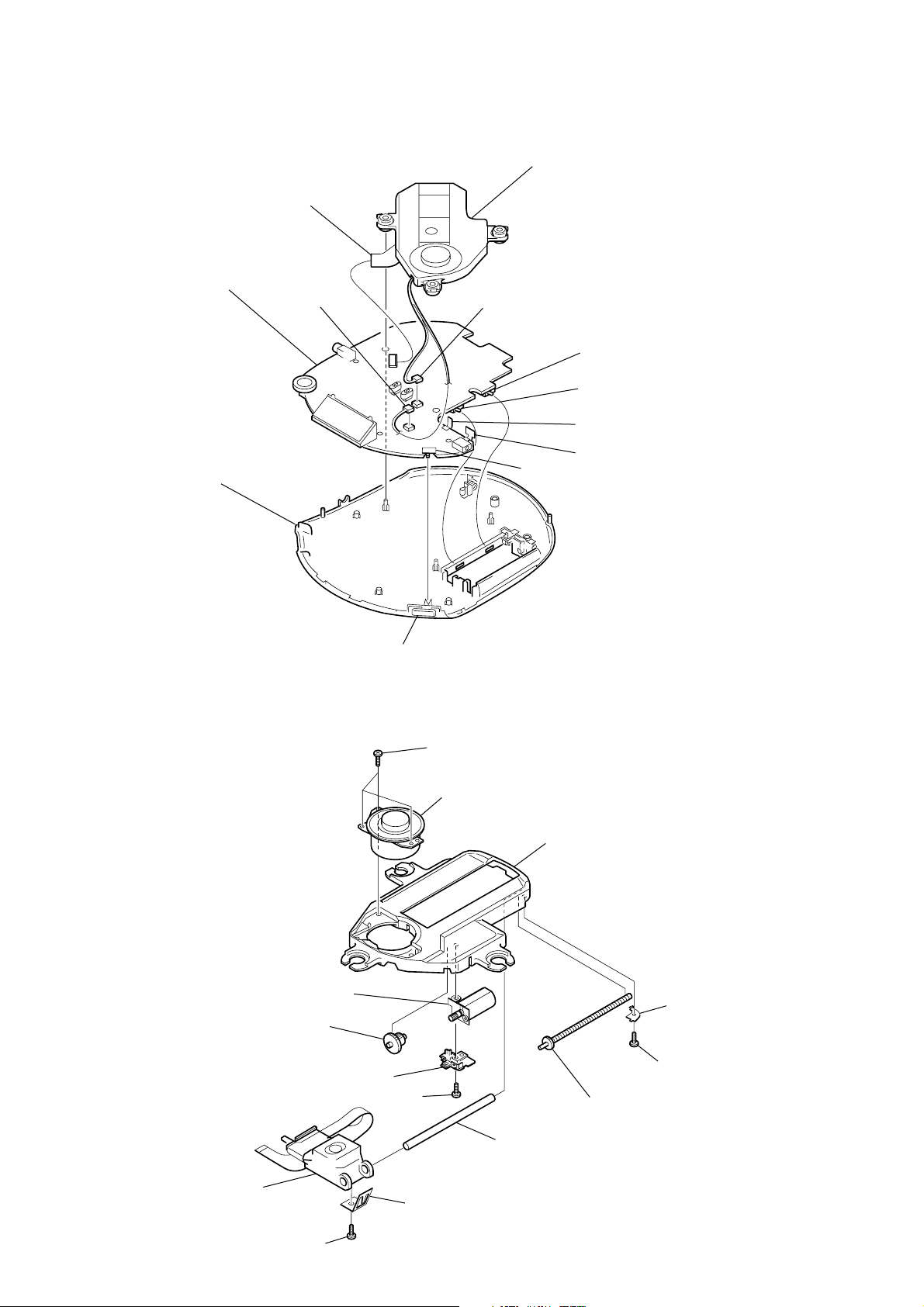
SECTION 3
y
y
DISASSEMBLY
Note : Follow the disassembly procedure in the numerical order given.
3-1. “LID, BATTERY CASE”, CABINET (FRONT) ASSY
8
1
B 2x10
D-F21/F22ST
0
cabinet (upper) ass
3-2. LID ASSY, UPPER
6
claws
7
claws
9
3
B 2x10
2
lid, battery case
2
lid assy, upper
4
claws
boss
5
claws
1
claws
cabinet (front) ass
5
Page 6
D-F21/F22ST
)
t
3-3. MAIN BOARD, MD ASSY
Note: When installing, fit the knob (HOLD) and S803.
1
CN501
7
MAIN board
cabinet (lower) sub assy
3
CN503
2
CN502
4
MD assy
S803
5
S812
6
S813
terminal (–), battery (BT402)
terminal (+.–), battery (BT400
3-4. OPTICAL PICK-UP, MOTOR
5
motor assy, sled (M501)
6
gear (B)
4
cover, gear
knob (HOLD)
3
B 1.7x5
1
B 1.7x5
2
motor assy, turntable (M502)
chassis
8
7
qa
screw (feed) assy
retainer, shaf
P 1.4x3.5
qd
shaft, standard
qs
pick-up block, optical
0
rack
9
B 1.4x2.3
6
Page 7
)
SECTION 4
ELECTRICAL ADJUSTMENTS
D-F21/F22ST
TUNER SECTION 0 dB = 1 µV
• FM Section
Setting:
RADIO ON•BAND/MEMORY button : FM
STEP switch : 10k
FM RF signal
generator
0.01
µ
F
75 kHz frequency
deviation by 1 kHz signal
output level : as low as possible
• AM Section
Setting:
RADIO ON•BAND/MEMORY button : AM
STEP switch : 10k
AM RF signal
generator
Put the lead-wire
antenna close to
the set.
TP3 (RF-IN)
set
FM FREQUENCY COVERAGE
CHECK
Frequency Display 87.5 MHz 108 MHz
Reading on Digital voltmeter 2.5 ± 1.5 V 7.0 ± 4.0 V
Adjustment Part <confirmation> <confirmation>
FM TRACKING ADJUSTMENT
Adjust for a maximum reading on level meter.
L2 CT1
87.5 MHz 108 MHz
AM IF ADJUSTMENT
Adjust for a maximum reading on level meter.
T1
450 kHz
AM FREQUENCY COVERAGE
CHECK
Frequency Display 530 kHz 1,710 kHz
Reading on Digital voltmeter 1.0 ± 0.5 V 5.2 ± 0.7 V
Adjustment Part <confirmation> <confirmation>
30% amplitude
modulation by
400 Hz signal
• Connecting Level Meter (FM and AM)
level meter
(range: 0.5–5 V ac
Ω
16
set
i
jack (J302)
• Connecting Digital Voltmeter (FM and AM)
digital
voltmeter
Ω
100 k
TP81 (VT)
AM TRACKING ADJUSTMENT
Adjust for a maximum reading on level meter.
L4 CT3
620 kHz 1,400 kHz
Adjustment Location: See page 8.
• Repeat the procedures in each adjustment several times, and the
frequency coverage and tracking adjustments should be finally
done by the trimmer capacitors.
• For FM adjustment, fix the FM RF coil (L1) as shown next page
and then perform tracking adjustment at L2 and CT1.
Lastly check the voltage value.
• For AM adjustment, fix the ferrite-rod antenna (L3) as shown
next page and then perform tracking adjustment at L4 and CT3.
Lastly check the voltage value.
7
Page 8
D-F21/F22ST
Adjustment Location:
– MAIN BOARD (SIDE A) –
CN501
AM IF ADJ
TP3
RF-IN
L3
L1
T1
CT1
FM TRACKING ADJ
L2
CT3 L4
AM TRACKING
ADJ
CD SECTION
CD section adjustments are done automatically in this set.
In case of operation check, confirm that focus bias.
FOCUS BIAS CHECK
1. Connect the oscilloscope between TP629 (RF) and GND on
main board.
2. Insert the disc (YEDS-18). (Part No. : 3-702-101-01)
3. Press the N X button.
4. Confirm that the oscilloscope waveform is as shown in the
figure below. (eye pattern)
A good eye pattern means that the diamond shape ( ) in the
center of the waveform can be clearly distinguished.
TP81
VT
IC61
Test Point:
– MAIN BOARD (SIDE B) –
• RF signal reference waveform (eye pattern)
VOLT/DIV : 20 mV (10 : 1 probe in use)
TIME/DIV : 500 nS
RF level :
±
0.1 Vp-p
0.45
When observing the eye pattern, set the oscilloscope for AC range
and raise vertical sensitivity.
8
TP629
RF
Page 9

SECTION 5
DIAGRAMS
5-1. IC PIN DESCRIPTIONS
• IC61 TC9327AF-631 (TUNER PLL, LCD DRIVER)
Pin No. Pin Name I/O Pin Description
1 – 4 COM1 – 4 O LCD driver signal output
5 – 20 S1 – 16 O LCD driver signal output
21 AM STEP-I I AM 9K/10K tuning step select signal input (initialization)
22 DEST2-I I Bit2 tuner destination setting signal input (Fixed at “L” in this set)
23 DEST1-I I Bit1 tuner destination setting signal input (Fixed at “L” in this set)
24 DEST0-I I Bit0 tuner destination setting signal input (Fixed at “L” in this set)
25 XLOCAL/XMONO-DET-I I LOCAL/DX or MONO/STEREO ON-OFF switch detect signal input
26, 27 NC — Not used. (Open)
28 LCDREQ-I I LCD display request signal input
29 LID OPEN I CD door open detect signal input
30 EEP D0/D1-IO I/O Data signal input/output for EEPROM IC.
31 EEP SK-O O Clock signal output for EEPROM IC.
32 EEP CS-O O Chip select signal output for EEPROM IC.
33 XL/O-I I Line out signal input
34, 35 NC — Not used. (Open)
36 MEM-KEY (3-BIT) I Memory key signal input (Fixed at “H” in this set)
37 PRESET KEY I Not used in this set. (Open)
38 CD ACK-I O CD acknowledge signal output
39 CDON-IWP-CDU I CD ON request signal input (Wake-up tuner in sleep mode)
40 I/O (RESERVED) — Not used. (Open)
41 NC — Not used. (Open)
42 AD1 KEY I Set keys signal input
43 AD2 RMKEY I Remote key signal input (Fixed at “L” in this set)
44 AD3 BATT HIDC I Battery/HiDC level detect signal input
45 AD DC REF I Reference DC signal input of A/D.
46 SDI-I-CDU I Serial data signal input from system control IC.
47 SDO-O-CDU (RESERVED) O Serial data signal output to system control IC.
48 SCK-I-CDU I Serial clock signal input from system control IC.
49 TUBEEP-O O Beep sound control signal output
50 NC (I/O) — Not used. (Open)
51 XHOLD-I-SW I HOLD detect signal input
52 XAVLS-I-SW I AVLS detect signal input
53 XDC IN DET-I I DC-in detect signal input
54 TU ON-O O Tuner ON request signal output
55 ST OR DX-O-CTR O LOCAL/DX or MONO/STEREO ON-OFF control signal output
56 TUBASS2-O O MEGA BASS 2 sound mode signal output (Not used in this set)
57 TU TEST MODE I Tuner test mode detect signal input
58 TUBASS1-O O MEGA BASS 1 sound mode signal output (Not used in this set)
59 AM/XFM-O O Band control FM/AM signal output to tuner IC.
60 +B ON/OFF O Radio power ON/OFF signal output
61 IFREQ-O O IF request signal output
62 TUMUTE-O O Mute HP control signal output
63 TEST — Not used. (Open)
64 IFIN I FM/AM IF signal input
65 EO (DO1) O PLL error signal output
66 NC (DO2) — Not used. (Open)
67 HOLD I Not used. (Connect to ground in this set)
68 NC — Not used. (Open)
69 GND — Ground
70 FM IN I FM oscillation signal input
D-F21/F22ST
9
Page 10

D-F21/F22ST
Pin No. Pin Name I/O Pin Description
71 AM IN I AM oscillation signal input
72 VDD (1.8-2.2V) — Power supply pin
73 RESET I Power reset signal input
74 XOUT O Crystal oscillation signal output (75 kHz)
75 XIN I Crystal oscillation signal input (75 kHz)
76 VXT — Crystal oscillation signal pin
77 VLCD — LCD voltage doubler
78, 79 C1, 2 — LCD voltage doubler
80 VEE — Constant voltage output to LCD.
10
Page 11

D-F21/F22ST
• IC801 TMP88CM22AF-3H31 (SYSTEM CONTROL)
Pin No. Pin Name I/O Pin Description
1 VSS — Ground
2 PWRSW O Headphone AMP IC power switch signal output
3 FOK I I Focus OK signal input from DSP IC. (“L”: NG, “H”: OK)
4 AGCPWM O O AGC control pulse signal output (Not used in this set)
5 CDON O O CD ON request signal output
6 SWEN2 O O CD/tuner select signal output
7 AMUTE O O Analog audio mute ON/OFF control signal output
8 VCC2ON O — Power supply pin (Not used in this set)
9 XRST O O Reset signal output to DSP IC.
10 SCK O O Serial data transfer clock signal output to DSP IC.
11 (SENS) SDTI I I Serial data signal input from DSP IC.
12 SDTO O O Serial data signal output to DSP IC.
13 SLPOUT O O WAKE-UP control signal output
14 AD CDTEST I CD test signal input (“L”: CD test) (Fixed at “H” in this set)
15 AD CHGMNT I Not used in this set. (Open)
16 AD RMKEY I Not used in this set. (Fixed at “L”)
17 AD BATMNT I Battery voltage detect signal input
18 AD CDKEY I Key signal input
19 AD RM INT I Not used in this set. (Open)
20 AD DCINMNT I DC-in voltage detect signal input (A/D input) and DC-in jack use/no use detect signal input.
21 WP OPEN I CD door open switch signal input
22 VREFL I Reference voltage signal input (0 V) for A/D converter.
23 VREFH I Reference voltage signal input (+2 V) for A/D converter.
24 VDD — Power supply pin (+2 V)
25 SCOR I I Sub-code sync (S0+S1) detect signal input from DSP IC.
26 GRSCOR I I GRSCOR signal input from DSP IC.
27 WFCK I I WFCK signal input from DSP IC.
28 BEEP O O Beep sound signal output to headphone AMP IC.
29 XCDRESET TU O O Reset signal output to DSP IC.
30 TUSCK O O Communication clock signal output to DSP IC.
31 (CD) SDI I I Communication data bus signal input from DSP IC.
32 (CD) SDO O O Communication data bus signal output to DSP IC.
33 RESERVE — Not used. (Open)
34 ACK CD I I CD acknowledge signal input
35 TUON I I Tuner ON request signal input
36 ESP I ESP switch signal input
37 L/O I I Line out signal input
38 AVLS I I AVLS switch signal input
39 HOLD I I HOLD switch signal input
40 CD-RW I Not used in this set. (Open)
41 ——Not used. (Open)
42 XHGON O O Not used in this set. (Open)
43 XTL O O Serial data latch pulse signal output
44 XSOE O O Serial data output enable signal output
45 TUVCPU O O Not used in this set. (Open)
46 POWLT O O Latch signal output to power control IC.
47 TUAUDIO O O Not used in this set. (Open)
48 XAPC OFF O O APC mute signal output (“L”: mute)
49 CDAUDIO O O Not used in this set. (Open)
50 RESERVE — Not used. (Open)
11
Page 12

D-F21/F22ST
Pin No. Pin Name I/O Pin Description
51 BASS1 O O Not used. (Fixed at “H” in this set)
52 BASS2 O O Not used. (Fixed at “H” in this set)
53 LCDREQ O O LCD display request signal output
54 – 64 SEG10 – 0 O Not used in this set. (Open)
65 – 68 COM3 – 0 O Not used in this set. (Open)
69 – 71 V3 – 1 O Not used in this set. (Open)
72, 73 C1, 0 O Not used in this set. (Open)
74 CDWP I I WAKE-UP control signal input
75 ICTEST I Test pin for IC. (Fixed at “L” in this set)
76 ——Not used. (Open)
77 ——Not used. (Fixed at “L” in this set)
78 RESET I I System reset signal input from power control IC. (“L”: reset)
79 XIN I I System clock signal input
80 XOUT O Not used in this set. (Open)
12
Page 13

5-2. BLOCK DIAGRAM — CD SECTION —
D-F21/F22ST
DETECTOR
A
B
RF
E
F
VCC
OPTICAL PICK-UP
BLOCK (DAX-23E)
FOCUS
COIL
TRACKING
COIL
LD
PD
M501
SLED
MOTOR
M502
SPINDLE
MOTOR
• Signal path
A
B
RF
E
M
M
: CD PLAY
MAIN BOARD (1/3)
CN501
13
12
11
7
F
F+
F–
T+
T–
LD
PD
8
6
4
1
2
3
10
Q403,405
9
CN503
1
S+
2
S–
1
C+
2
C–
CN502
LD
DRIVER
VCC1 +2V
FOCUS/TRACKING COIL DRIVER,
SPINDLE/SLED MOTOR DRIVE
IC401 (1/3)
FO2
28
DRIVER
RO2
26
FO3
23
DRIVER
RO3
21
RF2
63
INM2
64
RF21
59
PAPC
60
32
30
19
17
PD AMP
FO1
DRIVER
RO1
FO4
DRIVER
RO4
LEVEL
SHIFTER
CONTROLLER
LD AMP
RI1
RI2
RI3
PWM/FI4
PDL/RI4
VINDET
APCREF
FI1
33
34
FI2
35
36
FI3
13
14
SAW TOOTH
MDP
(Page 15)
12
11
COMPARATOR
IC401 (2/3)
COMP OUT
10
15
16
62
61
B+ +3V
+
(Page 15)
A
SYNC
62
61
58
71
59
60
46
47
50
51
42
43
44
B
48
A
B
RFDC
RFAC
E
F
SFDR
SRDR
FFDR
FRDR
TFDR
48
TRDR
49
C176
MDP
MDS
SDTO
XAPC_OFF_O
SCOR
17
SCOR_I
C
(Page 15)
SCK
DIGITAL SIGNAL PROCESSOR,
DIGITAL SERVO PROCESSOR
WDCK
WFCK
MDS
XTAO
XTAI
RFAC
SIGNAL
PROCESSOR
BLOCK
MDP
XSOE
SENS
R4M
XLAT
CLOK
SCOR
SDTO
RFDC
E
F
B
A
SDTO
SENS
CLOK
SDTI_I
SCK_O
(SENS)
SDTO_O
IC601
MEMORY
CONTROLLER,
BUS BOOST
BLOCK
SERVO
BLOCK
R4M
XSOE
WDCK
XLAT
242523
XLAT_O
WFCK
30 35
2826
78
83
26114443101225
79
27
XIN_I
WFCK_I
XSOE_O
GRSCOR_I
10
2
LPF
FOK
FFDR
FRDR
TFDR
TRDR
SFDR
SRDR
SYSTEM CONTROL
IC801 (1/3)
4
FOK
3
FOK_I
D0-D3
A0-A9
XRAS
XWE
XCAS
XOE
XTAI
XTAO
LOUT
ROUT
AMUTE
XRST
115 – 118
1-3, 5-7, 106-109
113
114
119
120
93
94
97
104
13
21
9
XRST_O
X601
16.9MHz
CD-L
CD-R
D
(Page
14)
A MUTE
13 13
Page 14

D-F21/F22ST
5-3. BLOCK DIAGRAM — TUNER SECTION —
MAIN BOARD (2/3
CT3
CT3,L4
AM
TRACKING
Q3
EXCEPT
)
(
F21:E13
)
D3
L3
AM
FERRITE-ROD
ANTENNA
VCPU+2V
D80
L4
TU VCC
22 4 6
2
TU VCC
AM OSC
AM
RF-IN
FM
RF-IN
FM
RF-OUT
20
AM
OSC
AM
MIX
D1 D2
CT1,L2
FM
TRACKING
FM
MIX
FM
OSC
21 1924
FM OSC
TU VCC
FM/AM FRONT-END,
MIX-OUT
OSC-OUT
T1
IF OSC
AMP
Q60
AM IF
L2L1 CT1
T81
IF DET,MPX
IC1
T1
TU VCC
TU VCC
CF1
7
CF3
DC/DC
CONVERTER
Q86
AM
IF-IN
FM
IF-IN
Q6
IF
BUFFER
IF-OUT
17
AM
DET
FM
DET
10
TU VCC
TU VCC
IF CUT
X1
10.7MHz
(Page 13)
DET-OUT
AF
BUFFER
16 15
LPF2(MAX/FM)
13 14
Q2
MPX-IN
Q1
(F21:E13)
D
FM
MPX
A MUTE
MUTE
IF CUT
LPF1(MONO/ST)
TU VCC
CD-L
CD-R
L-OUT
R-OUT
R-CH
12
11
R-CH
SIGNAL SELECT
8
11
TUNER/CD
IC303
12 6
D304
VDD+2V
D302
D601
9
10
RV301
VOLUME
14
19
20
17
LIN
MUTE
PWRSW
BEEP
HEADPHONE AMP
IC302
MT SW
PW SW
BEEP
LOUT
R-CH
12
ALCDET
8
R-CH
J302
i
LPF
Q84,85
55 65 53 71 70 61 64 59 6 7 2 28
EO(DO1)
ST OR DX-O-CTR
|
S1
COM1|COM4
5 – 201 – 4
LIQUID CRYSTAL
DISPLAY PANEL
LCD1
Signal path
: FM
: AM
: CD PLAY
S16
BUFFER
Q61
XDC IN
DEST2-I
DEST1-I
22 23 24
(EXCEPT F21:E13)
DET-I
XDCDT
DEST0-I
VCPU
(F21:E13)
(Page 15)
E
TUNER PLL,
LCD DRIVER
IC61
XOUT
74 75 45 32 31 30
Abbreviation
E13 : AC220-230V area in E model
X61
75kHz
XIN
AD DC REF
FM IN
AM IN
EEP CS-O
EEP SK-O
1 2 3
CS
SK
EEPROM
IC62
+1.6V REG.
IC81
B+ SWITCH
Q4,5
60
+B ON/OFF-O
EEP DO/D1-IO
DI
MONO ST
LOCAL DX
XLOCAL/XMONO-DET-I
25
S813
B+ +3V
IFREQ-O
(F21:E13)
(EXCEPT F21:E13)
IF IN
AM STEP-I
21
S812
STEP
9k 10k
(Page 15)
VCPU+2V
F
HIGH/BATT
AM/XFM-O
44
AD3_BATT_HIDC
OPEN
AVLS
HOLD
62 49 29
LID OPEN
TUBEEP-O
TUMUTE-O
73
RESET XCDRESET_TU-O
54
TU ON-O
33
XL/O-I
38
CD ACK-I
SDI-I-CDU
SCK-I-CDU
AD1_KEY
39
46
47
48
51
52
42
CDON-IWP-CDU
SDO-O-CDU
XHOLD-I-SW
XAVLS-I-SW
29
74
CDWP_I
L/O_I
37
ACK_CD_I
34
CDON_O
5
32
(CD)SDO_O
31
(CD)SDI_I
30
TUSCK_I
39
HOLD_I
38
AVLS_I
18
AD_CDKEY
SWEN2_O
KEY MATRIX
AMUTE_O
S805 - 811
PWRSW
SYSTEM CONTROL
IC801 (2/3)
BEEP_O
WP_OPEN
ESP
OPEN
21
AVLS
HOLD
36
VCPU+2V
S801
(CD DOOR OPEN)
S802
AVLS
NORM
LIMIT
S803
HOLD
OFF
ON
S804
ESP
OFF
ON
1414
Page 15

5-4. BLOCK DIAGRAM — POWER SUPPLY SECTION —
MAIN BOARD (3/3)
POWER CONTROL
IC401 (3/3)
D-F21/F22ST
VCC1+2V
VCPU +2V
VDD +2V
(Page 13)
(Page 13)
(Page 13)
B+
SWITCH
Q412
B+ SWITCH
Q406
B+ SWITCH
Q410
Q411
SYNC
A
SDTO
B
SCK
C
STNG
54
INP1
48
DTC1D
45
VLGO1
49
VCPU2 (2.0V)
42
VCPU1 (2.5V)
43
VCC1(2.5V)
44
SYNC
5
WAKEUP
6
DATA
8
CLOCK
7
LATCH
9
RSTB
4
VREF
58
VCPU2 (2.0V)
VCPU1 (2.5V)
VCC1
SWITCHING
POWER
CIRCUIT 2
CHARGE
CONTROL
CHG ON/OFF
CHARGE
SWITCH
CLK
OR OSC
INTERFACE
AMP
SAWTOOTH
GENERATOR
SWITCHING
POWER
CIRCUIT 5
STANDBY
REFERENCE
BANDGAP
REFERENCE
(VREF)
DC IN
VIN
CHGSW
RF4
DCIN
VG
BIAS
(Page 14)
HIGH/BATT
F
(Page 14)
XDCDT
E
53
FOCUS/TRACKING COIL DRIVER
SPINDLE/SLED MOTOR DRIVER
D407
DC IN
Q407
COMPARATOR
Q413
GATE
Q402
D405
SWITCH
Q401
D401
37
RS
38
40
L408
41
L4
1
VG
2
D406
DETECT
B+ +3V
(IC401) +3V,
HEADPHONE AMP
(IC302) +3V
L412
B+
B–
DRY BATTERY
SIZE "AA"
(IEC DESIGNATION LR6)
2PCS,3V
J401
DC IN 4.5V
!
13
SLPOUT_O
46
POWLT_O
SYSTEM CONTROL
WAKE-UP RESET
Q408,409
IC801 (3/3)
SWITCH
D801
17 20
78
RESET_I
AD_BATMNT
AD_DCINMNT
15 15
Page 16

D-F21/F22ST
5-5. PRINTED WIRING BOARD — MAIN SECTION —
• Semiconductor
Location (Side A)
Ref. No. Location
D1 G-4
D80 H-8
D82 H-8
D301 G-3
D302 G-2
D303 F-2
D304 F-2
D408 H-6
D461 H-6
D801 H-6
IC61 I-6
Q84 H-4
Q85 I-4
Q401 G-9
Q402 G-9
Q403 F-2
Q405 E-2
Q412 I-8
Common Note on Schematic Diagram:
• All capacitors are in µF unless otherwise noted. pF: µµF
50 WV or less are not indicated except for electrolytics
and tantalums.
• All resistors are in Ω and 1/
specified.
4
W or less unless otherwise
• % : indicates tolerance.
f
•
: internal component.
• C : panel designation.
Note: The components identified by mark 0 or dotted line
with mark 0 are critical for safety.
Replace only with part number specified.
• A : B+ Line.
• Total current is measured with CD installed.
• Power voltage is dc 4.5 V and fed with regulated dc power
supply from external power voltage jack.
• Voltages and waveforms are dc with respect to ground in
playback mode.
no mark : FM
( ) : AM
< > : CD
: Impossible to measure
∗
• Voltages are taken with a VOM (Input impedance 10 MΩ).
Voltage variations may be noted due to normal production tolerances.
• Waveforms are taken with a oscilloscope.
Voltage variations may be noted due to normal production tolerances.
• Circled numbers refer to wavefor ms.
• Signal path.
F : FM
f : AM
J : CD
• Abbreviation
E13 : AC 220 - 230V area in E model.
Common Note on Printed Wiring Boards:
• X : parts extracted from the component side.
• Y : parts extracted from the conductor side.
a
•
•
: Through hole.
f
: internal component.
• : Pattern from the side which enables seeing.
Caution:
Pattern face side: Parts on the pattern face side seen from the
(Side B) pattern face are indicated.
Parts face side: Parts on the parts face side seen from the
(Side A) parts face are indicated.
• Abbreviation
E13 : AC 220 - 230V area in E model.
A
B
C
D
E
F
G
H
I
J
1
2345678910
TAP801
R462
D801
C419
TP807
CN502
R461
R463
D461
R401
R402
C403
R410
D408
C423
(EXCEPT F21:E13)
R55
R56
R54
C461
C462
TP446
CN503
C411
R406
C401
TP401
R431
C412
R411
C401
R419
Q412
OPTICAL
PICK-UP
(DAX-23E)
1 WHT
2 BLK
1 BLK
2 RED
R407
R415
TP419
BLOCK
C451
C413
C430
C414
R854
SPINDLE
MOTOR
MOTOR
VDR402
R421
D80
C86
D82
R418
M502
M501
SLED
C85
Q402
R806
L412
Q401
R87
TP85
R88
T81
S803
R417
C450
VDR401
C87
R852
OFF ON
R857
S803
HOLD
R210
R110
TP630
C101
R500
R432
C500
R107
R429
D304
C421
C201
R404
R305
R207
Q405
R430
R405
Q403
R308
C360
R617
D303
D302
R645
R615
L312
R613
D301
C104
13
C204
R353
CN501
1
TAP1
C352
C318
TAP802
CT3
RF-IN
C42
TP3
C353
TP416
C13
TP620
TP502
TP504
TP503
C45
L6
C83
C33
R18
C68
R81
C24
C81
C63
TP30
FB12
R19
R80
C28
R82
C67
C82
TP501
TP31
C29
C47
TP81
R805
IC61
TP4
JC1
CT1
D1
R4
FB11
C71
Q84
R85
R5
R84
Q85
C64
1-681-838-12(12)
1616
Page 17

• Refer to page 16 for Common note on Printed Wiring Board.
D-F21/F22ST
J401
DC IN 4.5V
!
DRY BATTERY
SIZE "AA"
(IEC DESIGNATION LR6)
2PCS,3V
J401
S807
x
RADIO OFF
S808
>
TUNE +
S805
NX
C436
S807
TP806
TP810
R851
BT400
S808
S809
.
TUNE –
L411
TP424
R853
Q86
R91
C437
D404
C92
C90
TP82
TP422
C88
D401
C428
TP84
TP58
C452
C93
R86
L80
TP821
EXCEPT
F21 : E13
S805
R850
LOCAL
DX
TP421
TP410
TP811
R801
BT402
C405
R468
MONO
(F21 : E13)
R469
Q411
C409
C410
S809
S812
STEP
9k
10k
S813
ST
C408
R459
R409
C416
L402
C415
R483
C407
C417
R416
R482
R481
C406
33
48
C427
S813
S812
C418
R51
R53
D405
IC401
R423
TP814
R813
C805
R52
Q406
TP413
R440
R50
Q413
TP420
Q407
C95
L413
R424
R811
R820
C807
C810
TP809
TP71
C811
R802
R814
R458
R453
R454
R452
R455
R451
C453
R470
C420
R425
R450
TP820
LIMIT
NORM
C422
16
1
R408
R467
L408
Q408
IC62
D415
R422
Q410
TP406
R89
R25
S802
AVLS
TP19
TP59
R486
C432
C404
D406
Q61
(F21:E13)
D402
R449
1732
6449
C402
R63
TP411
LIQUID CRYSTAL DISPLAY PANEL
C804
IC801
R466
R442
TP21
Q4
R842
(F21:E13)
Q1
Q2
C39
Q6
C424
R412
R403
TP402
R48
C54
R57
LCD1
R804
R816
R464
L410
R47
C52
X1
R46
R803
Q5
D407
R12
R11
Q409
R42
R810
R822
C813
ON
OFF
C21
D409
C59
C58
C94
TP817
TP50
L409
R860
R845
C20
C16
IC81
TP803
S804
TP819
C19
C17
R60
R61
L61
R49
TP808
TP636
ESP
L2
C66
R41
R17
C18
R10
R9
C25
C27
C60
Q60
C61
C89
R15
TP13
R2
C2
C65
R640
C619
R643
R628
R639
C601
TP22
TP89
R831
R830
R829
R824
D602
VDR601
R16
R13
CF3
C26
IC1
C9
R3
TP10
C12
TP75
R62
C62
TP66
C97
1-681-838-
TP606
D601
TP603
TP604
R623
R624
R626
R627
TP616
R625
R630
L5
(EXCEPT F21:E13)
Q3
C36
R26
T1
CF1
TP18
C40
C38
C34
R1
D2
C46
C43
L4
C4
C15
C10
R64
TP23
X61
C620
R629
C621
R634
R636
C622
TP618
L601
TP5
C35
C44
C51
C57
TP805
R637
TP617
C23
TP20
C50
TP74
C69
C640
R638
L1
R7
C636
TP619
FL1
C5
12
12
R209
R202
R203
C202
IC601
C623
R641
C624
R646
TP33
TP32
L3
AM
FERRITE-
ROD
ANTENNA
L62
S806
BAND/MEMORY
VDR602
C635
C203
R204
TP627
C625
R632
TP623
TP624
TP626
TP628
TP625
TP1
TP816
R841
C76
S806
RADIO ON
C103
R104
C102
R650
C618
C637
CD DOOR
C841
S810
R859
R102
R103
R642
TP505
TP506
S801
OPEN
S801
D3
R858
R616
R614
R484
R621
R109
C612
C611
R485
TP812
MENU/
PRESET
C632
C613
C313
R855
S810
+
C631
FB602
R610
R603
R618
C319
TP639
C605
R606
C615
R612
R317
X601
C629
R605
R611
R856
C607
R609
C603
C614
C602
C354
C628
TP640
R620
R619
C351
FB603
C606
R608
TP311
C359
R607
R604
C626
TP111
IC303
IC302
TP635
C609
C604
C627
TP813
RV301
R651
TP407
FB111
VDR101
FB311
VDR303
S811
234567891011
C634
VDR201
C300
C350
R254
C254
RV301
VOLUME
TP629
TP211
R154
C154
C502
FB211
S811
SOUND/
PRESET
J302
–
1
A
B
C
D
E
J302
F
G
H
I
J
• Semiconductor Location (Side B)
Ref. No. Location Ref. No. Location
D2 H-5
D3 H-3
IC601 C-4
IC801 B-6
D401 G-9
D402 E-7
D404 G-9
D405 E-7
D406 H-6
D407 E-6
D409 H-6
D415 E-6
D601 C-5
D602 C-5
Q1 G-6
Q2 G-6
Q3 E-5
Q4 E-6
Q5 D-6
Q6 G-6
Q60 I-5
Q61 I-6
Q86 H-9
Q406 D-7
IC1 G-5
IC62 I-7
IC81 I-6
IC302 G-2
IC303 G-2
IC401 H-7
Q407 E-7
Q408 H-6
Q409 H-6
Q410 E-6
Q411 G-8
Q413 E-7
17 17
Page 18

D-F21/F22ST
5-6. SCHEMATIC DIAGRAM — MAIN SECTION (1/3) —• Refer to page 21 for IC Block Diagrams.
• Refer to page 16 for Common Note on Schematic Diagram.
R81
TP10
L3
TP20
D3
R5
C10
C15
C13
CT3
R7
C44
C43
L6
C71
L4
C4
C51
R19
C5
R4 R3
D1
CT1L1
C45
R18
C40
FB11
IC B/D
IC1
TAP1
TP3
TP1
C50
FL1
C23C42
Q3
C36
(F21:E13)
R26
C38
Q1
R11
TP5
TP4
(EXCEPT F21:E13)
R16
C9
C2
D2
R1
C46
C34
C33
FB12
TP18
C26
C12
R9
R2
L2
C35
T1
JC1R13
CF1
TP81
C39
R10
C19
C17
C47
C18
C24
C27
TP22
CF3
Q6
C20
R12
C21
C25
X1
C28 C29
TP59
C16
TP19
Q2
TP13
TP31 TP33
TP30 TP32
R15
C81
R82
TP21
L5
TP2
TP89
C89
C82
Q85
Q5
IC81
R17
R87
Q4
TP82
R89
Q61
R25
C95
L80
R91
Q86
D80
C87
T81
R88
C86
C52
R48
(Page 19)
(Page 20)
R62
C83
TP66
R49
C59
L61
R60
C60
R61
TP74
L62
Q60
C58
C69
C76
C57
R80
TP23
C61
C62
R64
C97
C63
C64
C65
X61
C66
C68
C67
R42
R41
IC61
C94
R46
(EXCEPT F21:E13)
R47
R55
R56
R54
R57
(F21:E13)
TP50
TP71
R63
R50
R53
R51
R52
IC62
S812
TP58
C54
S813
(F21:E13)
(EXCEPT F21:E13)
R84
R85
Q84
• Waveforms (CD play mode)
200mV/div 5µsec/div
1
IC61
75kHz
LCD1
(XOUT)
uf
D82
C85
0.7Vp-p
C90
C92
2
R86
C93C88
TP84TP85
1V/div 0.2µsec/div
34nsec
Q86
C
3.6Vp-p
TP75
1818
Page 19

5-7. SCHEMATIC DIAGRAM — MAIN SECTION (2/3) — • Refer to page 21, 22 for IC Block Diagrams.
• Refer to page 16 for Common Note on Schematic Diagram.
D-F21/F22ST
C500
CN501
CN503
CN502
TP504
C502
R429
TP506
TP505
TP503
Q403
TP502
TP501
R430
Q405
C421
R405
D301
D601
R637
R628
R639
R643
R627
R603
C603
C604
R604
R606
R605
R607
R626
R625
C619
R640
VDR601
R624
C620
R608
C607
C606
R609
R610
C605
R623
IC601
TP604 TP603
TP636
D602
C628
IC B/D
TP639
TP640
R629
TP617
TP618
TP619
R638
R641
C621
C622
R632
TP635
R612
C627
L601
C601
C626
TP616
C602
R630
TP620
C625
C623
R646
C624
TP623
TP625
TP627
R642
TP629
R645
R613
R615
TP406TP407
R500
R404
R485
R484
R617
R619
R651
C609
C615
R611
R620
C614
TP630
R618
TP624
TP626
TP628
C613
R616
C618
C612
R614
C637
C611
TP606
R650
C636
C102
C629
FB602
R621
R204
R636
C202
R203
R103
C631
R102
X601
R104
R202
R210
C203
R209
C103
R109
FB603
C635
R634
C634
VDR602
C632
C640
D302
R308
C201
R207
C204
C104
R317
C353
C352
C360
C351
RV301
R110
IC303
IC B/D
IC302
VDR201
C101
R107
VDR101
D303
D304
R305
VDR303
C350
FB211
FB111
L312
R353
(Page 18)
TP211
TP111
J302
FB311
TP311
C313
C154R154
C300
C254R254
C354
C359
R432
• Waveforms (CD play mode)
100mV/div 0.5µsec/div
3
0.45Vp-p
TP629 (RF)
500mV/div 5µsec/div
4
ih
IC601
2.0Vp-p
22.5µsec
(LRCK)
500mV/div 0.02µsec/div
5
16.9MHz
(XTAO)
of
IC601
(Page 20)
2.0Vp-p
19 19
Page 20

D-F21/F22ST
5-8. SCHEMATIC DIAGRAM — MAIN SECTION (3/3) —• Refer to page 23 for IC Block Diagrams.
• Refer to page 16 for Common Note on Schematic Diagram.
(Page 19)
TP410
TP419
TP416
TP411
R468
C430
R411
Q402
R417
Q406
Q410
R450R440
R449
Q411
C405
R469
R407
C407
C410
C409
C408 R409
D401
Q401
D405
C412
TP401
Q412
C413
R415
R459
R416
R418
R431
C414
R421
R419
L402
C416C415
C428
C420
C417
Q413
D415
R422
D402
L410 L409
L401
C411
R406
C418
C401
R453
IC401
TP446
R425
TP417
R424
R442
Q407
D407
R423
C427
TP420
L413
C406
IC B/D
R401
R402
C403
C402
R470
R464
R466R454
R467
L408
D406
TP402
C404
C451
C422
R408
D408
TP421
R461
D461
Q408
C419
C423
R410
VDR402
R462
R486
TP413
D801
R463
Q409
C462
C432
C453
R451
R452
R458
C461
R412
D409
R805
R403
R455
R481
R482
R483
C424
C318
C319
R802
R814
R822
R816
C811
R824
R829
R830
R831
TP812
R856 R855 R853 R857 R851
TP813
S811
R858
S810
R859
TP811
S809
R854
TP810
R810
IC801
S808
R804
R803
C804
TP806
R852
S807 S806 S805
C810
R813
TP809
TP821TP805
R850
TAP801
R811
TP814
C805
C807
R820
TP803
R860
TP807
C452
TAP802
L411
R842
TP817
R801
L412
C436
D404
TP820
TP808
TP819
TP422
TP424
R841
TP816
C841
R845
C813
R806
TP818
C450
C437
VDR401
(Page 18)
S801
S802
S803
S804
BT400
BT401
BT402
J401
• Waveforms (CD play mode)
1V/div 0.2µsec/div
6
3.6Vp-p
0.235µsec
IC801
(XIN_1)
ul
2020
Page 21

5-9. IC BLOCK DIAGRAMS
IC1 TA2149BFN
D-F21/F22ST
RF GND
FM IN
AM L/CUT
MIX OUT
VCC
AF IF
FM IF
GND
AGC
QUAD
R-OUT
L-OUT
24
1
FM RF
2
3
4
5
6
FM IF
7
8
AGC
9
10
11
MUTE
12
AM IF
FM
MIX
MIX
AM
LEVEL
DET
AM
DET
FM
DET
ST/MO
FM/AM
FM
OSC
AM
OSC
BUFF
BUFF
IF BUFF
1/8
AF BUFF
VCO
DIVIDE
DECODE
ST
SW
IF REQ
1/1 OR
1/16
AF
FM RF
23
RF VCC
AM RF
22
FM OSC
21
AM OSC
20
19
OSC OUT
XST DET
18
XIFREQ
17
16
DET OUT
MPX IN
15
14
LPF1 XMO/ST
13
LPF2 XAM/FM
IC302 TA2120FN
BB
BST
SW
OUT
24
23
ADDB
BST
+
–
2
1
BSTNFADD
OUT
ADD
BIAS
IN
BIAS
22
BIAS
A
PWC
3
RF IN OCL
SW
SW
PWR
SW
20
21
4
19
PWSWMT
SW
+
–
PW
B
5
6
VCC
ROUT VREF LOUT PGND MIX
18
ROUT
PW
C
7
BEEPMUTE MUTE_γ
17
BEEP
+
PW
15
16
ALC ALC
LOUT
–
A
8
10
9
OUT
ATT
LINRINGND
SW
14
ATT
SW
ALC
DET
11
ALCINALC
DET
13
12
21
Page 22

D-F21/F22ST
IC601 CXD3037R
XOE
XCASD2D3D0D1
120 119 118 117 116 115 114 113 112 111 110 109 108 107 106 105 104 103 102 101 100 99 98 97 96 95 94 93 92 91
D2D3D0
XOE
XCAS
XWE
XRAS
A11
A10
DVDD(2.5V)A0A1A2A3
A11
A10
DVDD
A0A1A2
D1
XWE
XRAS
AVDD2(2.5V)
A3
AVDD2
ROUT
AIN2
LOUT2
AIN2
AOUT2
AVSS2
AOUT2
AVSS2
AVSS1
AVSS1
AOUT1
AOUT1
AIN1
AIN1
LOUT
AVDD1(2.5V)
LOUT1
AVDD1
XVSS
XVSS
XTAO
XTAO
XTAI
XTAI
XVDD
XVDD
BCKI
BCKI
DVSS
XWRE
XRDE
XEMP
XWIH
XQOK
AMUTE
SDTI
XQCK
SCSY
SCOR
VSS0
SBSO
EXCK
XRST
SYSM
SDTO
XLAT
CLOK
SENS
SCLK
XSOE
ATSK
R4M
VPCO
WFCK
DEMODULATOR
CONVERTER
GFS
MDS
XUGF
EFM
SUB CODE
PROCESSOR
SERVO
AUTO
SEQUENCER
A/D
ERROR
CORRECTOR
32K
RAM
PROCESSOR
C2PO
D/A
INTERFACE
SIGNAL
BLOCK
SERVO
INTERFACE
MIRR
DFCT
FOK
SERVO DSP
FOCUS SERVO
TRACKING
SERVO
SLED SERVO
WDCK
VIBRATION
MEMORY
CONTROLLER
+
COMPRESSION
EXPANDER
DAC
MEMORY CONTROLLER,
BUS BOOST BLOCK
LPF
LPF
PWM GENERATOR
FOCUS PWM
GENERATOR
TRACKING PWM
GENERATOR
SLED PWM
GENERATOR
SELECTOR
DIGITAL
OUT
XOE
XCAS
XWE
XRAS
XQOK
XWIH
XEMP
XRDE
XWRE
D0 – D4
A0 – A11
SYSM
AMUTE
HPL/HP
HPM
HPR
PCMDI
LRCKI
BCKI
AOUT1
AIN1
LOUT1
LOUT2
AIN2
AOUT2
ATSK
SCLK
SSTP
COUT
DFCT
MIRR
SRDR
FOK
FRDR
FFDR
TRDR
TFDR
SFDR
BCK
PCMD
LRCK
DOUT
BCK
PCMDI
PCMD
LRCKI
LRCK
DOUT
VDD2
WFCK
C2PO
GFS
XPCK
XUGF
WDCK
VSS2
XTSL
AVDD3
ASYO
ASYI
BIAS
RFAC
AVSS3
CLTV
PCO
FILI
FILO
VCTL
VPCO
VC
A
B
90
BCK
89
PCMDI
88
PCMD
87
LRCKI
86
LRCK
85
DOUT
84
VDD2(2.0V)
83
WFCK
82
C2PO
81
GFS
80
XPCK
79
XUGF
78
WDCK
77
VSS2
76
XTSL
75
AVDD3(2.0V)
74
ASYO
73
ASYI
72
BIAS
71
RFAC
70
AVSS3
69
CLTV
68
PCO
67
FILI
66
FILO
65
VCTL
64
VPCO
63
VC
62
A
61
B
XTAI
XTSL
VCTL
XTAO
CLOCK
GENERATOR
RFAC
BIAS
ASYMMETRY
ASYI
CORRECTOR
ASYO
FILO
FILI
DIGITAL
PCO
CLTV
XPCK
A9
1
A9
A8
2
A8
A7
3
A7
DVSS
4
A6
5
A6
A5
6
A5
A4
7
A4
XWRE
8
XRDE
9
XEMP
10
XWIH
11
XQOK
12
AMUTE
13
SDTI
14
15
SCSY
16
SCOR
17
VSS0
18
SBSO
19
EXCK
20
21
SYSM
22
SDTO
23
XLAT
24
CLOK
25
SENS
26
SCLK
27
XSOE
28
ATSK
29
R4M
30
PWMI
MDP
SDTI
SCSY
SCOR
SBSO
EXCK
SDTO
XLAT
CLOK
SENS
XSOE
R4M
IGEN
RFDC
VC
D GND
SERVO BLOCK
E
F
B
A
PLL
DIGITAL
CLV
CPU
INTERFACE
OP AMP
ANALOG SWITCH
22
D VDD
FOK
HPR
PWMI
FOK
LOCK/HPL
PWMI/HPVSS
HPR
HPM
HPM
DFCT
MIRR
VDD0
COUT
31 32 33 34 35 36 37 38 39 40 41 42 43 44 45 46 47 48 49 50 51 52 53 54 55 56 57 58 59 60
DFCT
MIRR
VDD0
COUT
MDP
VDD1
HPL/HP
MDP
C176
VDD1(2.0V)
HPL/HPVDD(2.5V)
MDS
MDS
SSTP
SSTP
SFDR
SFDR
SRDR
SRDR
TFDR
TFDR
TRDR
TRDR
FFDR
FFDR
FRDR
FRDR
VSS1
VSS1
TEST
A VDD
IGEN
AVDD0
TES1
AVDD0(2.5V)
IGEN
A GND
AVSS0
AVSS0
RFDC
RFDC
E
E
F
F
Page 23

IC401 TB2125F
49
VLGO1
50
L1L
51
PGND1
52
L1H
53
VIN
54
STNG
55
BATM1
56
BATM2
57
CHGMNT
58
VREF
59
RF21
60
PAPC
61
APCREF
62
VINDET
63
RF2
64
INM2
VCPU
VCPU
VCPU
VG
VG
VG
VG
R-2
VCPU
VCPU
R-4
VREF VIN
VREF
INP1
48
47
SAW TOOTH
VCPU2
R-5
RF1
VCPU
VCPU
46
VIN
SUB VREF
VIN
VCPU
STANDBY
REFERENCE
VCPU
1/2 VREF
BANDGAP
REFERENCE
(VREF)
VG
VCPU
INM1
VREF
VCPU
VCPU
VG
VCPU
DTC1D
45
VCC1
S-2
CLK
VCC1(2.5V)
44
VG
VREF
VCPU1(2.5V)
43
VCPU
R-6
DCIN
VCPU2(2.0V)
42
VCPU
SUB VREF
SAW GEN
OR OSC
S-1
INTERFACE
DCIN
VREF
VCPUCLK
S-3
VCPU
CLK
VCPU
BIAS
VCPU
D-F21/F22ST
DCIN
RF4
INM4
RS
41
40
39
38
DCIN
VCPU2
R-1
DCIN
VCPU2
VREF
SAW TOOTH
VCPU2
VCPU
D-5
VREF
CHGSW
37
CONTROL
CHARGE
CHGON/OFF
OEB
CONTROLLER
DCIN
RI2
FI2
36
35
34
VG
LEVEL
SHIFTER
D-1 to 4
RI1
FI1
33
FO1
32
H BRIDGE
DRIVER 1
H BRIDGE
DRIVER 2
H BRIDGE
DRIVER 3
H BRIDGE
DRIVER 4
31
30
29
28
27
26
25
24
23
22
21
20
19
18
17
MGND1
RO1
VD12
FO2
MGND2
RO2
VD23B
VD23A
FO3
MGND3
RO3
VD34
FO4
MGND4
RO4
1
2
3
L4
VG
GND
4
RSTB
5
SYNC
6
WAKEUP
7
CLOCK
8
DATA
9
LATCH
10
COMP OUT
11 12
MDP
13
14
FI3
RI3
SAW TOOTH
15
16
PWM/FI4
PDL/RI4
23
Page 24

D-F21/F22ST
NOTE:
• The mechanical parts with no reference
number in the exploded views are not supplied.
• Items marked “*” are not stocked since
they are seldom required for routine service.
Some delay should be anticipated
when ordering these items.
6-1. CABINET (FRONT) SECTION
SECTION 6
EXPLODED VIEWS
• Color Indication of Appearance Parts
Example :
KNOB, BALANCE (WHITE) ... (RED)
RR
Parts Color Cabinet’s Color
• Accessories are given in the last of this parts list.
• Abbreviation
E13 : AC 220 - 230V area in E model
1
The components identified by
mark 0 or dotted line with mark
0 are critical for safety.
Replace only with part number
specified.
2
3
5
4
2
6
Ref. No. Part No. Description Remark
1 X-3380-752-1 LID ASSY, UPPER (F22ST)
1 X-3381-520-2 LID ASSY, UPPER (F21)
2 3-336-395-01 SCREW (B2X10) (G), TAPPING
3 X-3380-754-1 CABINET (FRONT) SUB ASSY
24
Ref. No. Part No. Description Remark
4 3-231-897-01 BUTTON (OPEN)
5 3-232-612-01 KNOB (JOGGABLE)
6 3-231-037-02 LID, BATTERY CASE (EXCEPT F21:E13)
6 3-231-037-11 LID, BATTERY CASE (F21:E13)
Page 25

6-2. CABINET (LOWER) SECTION
D-F21/F22ST
CDM-3123EBA
64
59
LCD1
53
51
51
62
54
63
55
58
51
52
56
57
61
Ref. No. Part No. Description Remark Ref. No. Part No. Description Remark
51 4-222-765-11 INSULATOR
* 52 A-3021-498-A MAIN BOARD, COMPLETE (EXCEPT F21:E13)
* 52 A-3021-691-A MAIN BOARD, COMPLETE (F21:E13)
53 3-231-036-01 HOLDER, LCD
54 3-231-411-01 TERMINAL (–), BATTERY (BT402)
55 3-222-860-01 TERMINAL (+.–), BATTERY (BT400)
56 4-218-592-01 CUSHION
57 3-231-676-01 TERMINAL (LINK 4), BATTERY (BT401)
58 3-222-862-01 SPRING (TORSION)
59 X-3380-753-1 CABINET (LOWER) SUB ASSY
60 3-222-857-01 KNOB (HOLD)
61 4-974-607-11 FOOT, RUBBER
* 62 3-232-351-03 PAPER, SHIELD
63 3-234-025-01 SHEET, INSULATING
64 3-234-026-01 PAPER (CABINET), SHIELD
LCD1 1-804-462-11 DISPLAY PANEL, LIQUID CRYSTAL
60
25
Page 26

D-F21/F22ST
6-3. CD MECHANISM DECK SECTION
(CDM-3123EBA)
109
M502
101
108
112
107
111
110
109
106
M501
105
102
104
103
The components identified by
mark 0 or dotted line with mark
0 are critical for safety.
Replace only with part number
specified.
Ref. No. Part No. Description Remark Ref. No. Part No. Description Remark
101 4-218-820-01 CHASSIS
102 4-218-827-02 RETAINER, SHAFT
103 3-686-458-03 SCREW (P1.4X3.5), TAPPING
104 A-3328-628-A SCREW (FEED) ASSY
105 4-220-645-02 SHAFT, STANDARD
106 4-223-600-01 RACK
107 3-895-823-61 SCREW (B1.4X2.3), TAPPING
0 108 X-4952-506-1 PICK-UP BLOCK, OPTICAL (DAX-23E)
109 3-318-203-71 SCREW (B1.7X5), TAPPING
110 4-218-821-01 COVER, GEAR
111 4-218-823-01 GEAR (B)
112 4-218-825-01 SPRING, SLED
M501 A-3328-627-A MOTOR ASSY, SLED (SLED)
M502 A-3328-759-A MOTOR ASSY, TURNTABLE (SPINDLE)
26
Page 27

D-F21/F22ST
SECTION 7
ELECTRICAL PARTS LIST
NOTE:
• Due to standardization, replacements in
the parts list may be different from the
parts specified in the diagrams or the
components used on the set.
• RESISTORS
All resistors are in ohms.
METAL:Metal-film resistor.
METAL OXIDE: Metal oxide-film resistor.
F:nonflammable
• Items marked “*” are not stocked since
they are seldom required for routine service.
Some delay should be anticipated
when ordering these items.
Ref. No. Part No. Description Remark Ref. No. Part No. Description Remark
* A-3021-498-A MAIN BOARD, COMPLETE (EXCEPT F21:E13)
* A-3021-691-A MAIN BOARD, COMPLETE (F21:E13)
*********************
3-231-036-01 HOLDER, LCD
* 3-232-351-03 PAPER, SHIELD
3-234-025-01 SHEET, INSULATING
3-222-860-01 TERMINAL (+.–), BATTERY (BT400)
3-231-411-01 TERMINAL (–), BATTERY (BT402)
< CAPACITOR >
• SEMICONDUCTORS
In each case, u : µ, for example:
uA.. : µA.. uPA.. : µPA..
uPB.. : µPB.. uPC.. : µPC.. uPD.. : µPD..
• CAPACITORS
uF : µF
• COILS
uH : µH
• Abbreviation
E13 : AC 220 - 230V area in E model
E92 : AC 120V area in E model
MX : Mexican model
C50 1-115-416-11 CERAMIC CHIP 0.001uF 5% 25V
C51 1-164-156-11 CERAMIC CHIP 0.1uF 25V
C52 1-164-156-11 CERAMIC CHIP 0.1uF 25V
C54 1-115-156-11 CERAMIC CHIP 1uF 10V
C57 1-126-154-11 ELECT 47uF 20% 6.3V
C58 1-162-970-11 CERAMIC CHIP 0.01uF 10% 25V
C59 1-162-970-11 CERAMIC CHIP 0.01uF 10% 25V
C60 1-162-927-11 CERAMIC CHIP 100PF 5% 50V
C61 1-162-927-11 CERAMIC CHIP 100PF 5% 50V
C62 1-115-416-11 CERAMIC CHIP 0.001uF 5% 25V
The components identified by
mark 0 or dotted line with mark
0 are critical for safety.
Replace only with part number
specified.
When indicating parts by reference
number, please include the board.
MAIN
C2 1-162-917-11 CERAMIC CHIP 15PF 5% 50V
C4 1-162-917-11 CERAMIC CHIP 15PF 5% 50V
C5 1-115-416-11 CERAMIC CHIP 0.001uF 5% 25V
C9 1-162-970-11 CERAMIC CHIP 0.01uF 10% 25V
C10 1-162-959-11 CERAMIC CHIP 330PF 5% 50V
C12 1-162-927-11 CERAMIC CHIP 100PF 5% 50V
C13 1-164-227-11 CERAMIC CHIP 0.022uF 10% 25V
C15 1-162-923-11 CERAMIC CHIP 47PF 5% 50V
C16 1-162-970-11 CERAMIC CHIP 0.01uF 10% 25V
C17 1-115-156-11 CERAMIC CHIP 1uF 10V
C18 1-162-964-11 CERAMIC CHIP 0.001uF 10% 50V
C19 1-107-826-11 CERAMIC CHIP 0.1uF 10% 16V
C20 1-109-982-11 CERAMIC CHIP 1uF 10% 10V
C21 1-164-156-11 CERAMIC CHIP 0.1uF 25V
C23 1-162-962-11 CERAMIC CHIP 470PF 10% 50V
C24 1-162-970-11 CERAMIC CHIP 0.01uF 10% 25V
C25 1-124-635-00 ELECT 220uF 20% 6.3V
C26 1-125-837-11 CERAMIC CHIP 1uF 10% 6.3V
C27 1-117-720-11 CERAMIC CHIP 4.7uF 10V
C28 1-164-227-11 CERAMIC CHIP 0.022uF 10% 25V
C29 1-164-227-11 CERAMIC CHIP 0.022uF 10% 25V
C33 1-162-970-11 CERAMIC CHIP 0.01uF 10% 25V
C34 1-162-964-11 CERAMIC CHIP 0.001uF 10% 50V
C35 1-104-852-11 TANTAL. CHIP 22uF 20% 10V
C36 1-162-970-11 CERAMIC CHIP 0.01uF 10% 25V
(EXCEPT F21:E13)
C38 1-162-970-11 CERAMIC CHIP 0.01uF 10% 25V
C39 1-162-970-11 CERAMIC CHIP 0.01uF 10% 25V
C40 1-162-970-11 CERAMIC CHIP 0.01uF 10% 25V
C42 1-216-864-11 METAL CHIP 0 5% 1/16W
C43 1-164-227-11 CERAMIC CHIP 0.022uF 10% 25V
C44 1-164-227-11 CERAMIC CHIP 0.022uF 10% 25V
C45 1-162-970-11 CERAMIC CHIP 0.01uF 10% 25V
C46 1-162-964-11 CERAMIC CHIP 0.001uF 10% 50V
C47 1-162-970-11 CERAMIC CHIP 0.01uF 10% 25V
C63 1-162-919-11 CERAMIC CHIP 22PF 5% 50V
C64 1-162-917-11 CERAMIC CHIP 15PF 5% 50V
C65 1-113-619-11 CERAMIC CHIP 0.47uF 10V
C66 1-107-826-11 CERAMIC CHIP 0.1uF 10% 16V
C67 1-107-826-11 CERAMIC CHIP 0.1uF 10% 16V
C68 1-113-619-11 CERAMIC CHIP 0.47uF 10V
C69 1-124-584-00 ELECT 100uF 20% 10V
C71 1-162-964-11 CERAMIC CHIP 0.001uF 10% 50V
C76 1-162-970-11 CERAMIC CHIP 0.01uF 10% 25V
C81 1-115-416-11 CERAMIC CHIP 0.001uF 5% 25V
C82 1-164-489-11 CERAMIC CHIP 0.22uF 10% 16V
C83 1-162-927-11 CERAMIC CHIP 100PF 5% 50V
C85 1-164-505-11 CERAMIC CHIP 2.2uF 16V
C86 1-162-915-11 CERAMIC CHIP 10PF 0.5PF 50V
C87 1-162-915-11 CERAMIC CHIP 10PF 0.5PF 50V
C88 1-162-970-11 CERAMIC CHIP 0.01uF 10% 25V
C89 1-164-505-11 CERAMIC CHIP 2.2uF 16V
C90 1-104-852-11 TANTAL. CHIP 22uF 20% 10V
C92 1-162-970-11 CERAMIC CHIP 0.01uF 10% 25V
C93 1-162-964-11 CERAMIC CHIP 0.001uF 10% 50V
C94 1-164-156-11 CERAMIC CHIP 0.1uF 25V
C95 1-126-153-11 ELECT 22uF 20% 6.3V
C97 1-107-826-11 CERAMIC CHIP 0.1uF 10% 16V
C101 1-109-982-11 CERAMIC CHIP 1uF 10% 10V
C102 1-164-217-11 CERAMIC CHIP 150PF 5% 50V
C103 1-162-963-11 CERAMIC CHIP 680PF 10% 50V
C104 1-162-962-11 CERAMIC CHIP 470PF 10% 50V
C154 1-107-826-11 CERAMIC CHIP 0.1uF 10% 16V
C201 1-109-982-11 CERAMIC CHIP 1uF 10% 10V
C202 1-164-217-11 CERAMIC CHIP 150PF 5% 50V
C203 1-162-963-11 CERAMIC CHIP 680PF 10% 50V
C204 1-162-962-11 CERAMIC CHIP 470PF 10% 50V
C254 1-107-826-11 CERAMIC CHIP 0.1uF 10% 16V
C300 1-125-838-11 CERAMIC CHIP 2.2uF 10% 6.3V
C313 1-104-852-11 TANTAL. CHIP 22uF 20% 10V
27
Page 28

D-F21/F22ST
MAIN
Ref. No. Part No. Description Remark Ref. No. Part No. Description Remark
C318 1-164-156-11 CERAMIC CHIP 0.1uF 25V
C319 1-164-156-11 CERAMIC CHIP 0.1uF 25V
C350 1-115-156-11 CERAMIC CHIP 1uF 10V
C351 1-162-970-11 CERAMIC CHIP 0.01uF 10% 25V
C352 1-135-854-21 ELECT CHIP 10uF 20% 16V
C607 1-125-891-11 CERAMIC CHIP 0.47uF 10% 10V
C609 1-162-967-11 CERAMIC CHIP 0.0033uF 10% 50V
C611 1-162-917-11 CERAMIC CHIP 15PF 5% 50V
C612 1-162-962-11 CERAMIC CHIP 470PF 10% 50V
C613 1-162-962-11 CERAMIC CHIP 470PF 10% 50V
C353 1-135-854-21 ELECT CHIP 10uF 20% 16V
C354 1-137-934-11 TANTAL. CHIP 47uF 20% 10V
C359 1-109-982-11 CERAMIC CHIP 1uF 10% 10V
C360 1-162-970-11 CERAMIC CHIP 0.01uF 10% 25V
C401 1-162-970-11 CERAMIC CHIP 0.01uF 10% 25V
C402 1-164-505-11 CERAMIC CHIP 2.2uF 16V
C403 1-162-927-11 CERAMIC CHIP 100PF 5% 50V
C404 1-104-913-11 TANTAL. CHIP 10uF 20% 16V
C405 1-115-156-11 CERAMIC CHIP 1uF 10V
C406 1-128-057-11 ELECT 330uF 20% 6.3V
C407 1-162-964-11 CERAMIC CHIP 0.001uF 10% 50V
C408 1-162-919-11 CERAMIC CHIP 22PF 5% 50V
C409 1-124-584-00 ELECT 100uF 20% 10V
C410 1-124-584-00 ELECT 100uF 20% 10V
C411 1-801-862-11 VARISTOR (CHIP TYPE)
C412 1-164-156-11 CERAMIC CHIP 0.1uF 25V
C413 1-162-970-11 CERAMIC CHIP 0.01uF 10% 25V
C414 1-162-966-11 CERAMIC CHIP 0.0022uF 10% 50V
C415 1-164-156-11 CERAMIC CHIP 0.1uF 25V
C416 1-164-156-11 CERAMIC CHIP 0.1uF 25V
C417 1-110-569-11 TANTAL. CHIP 47uF 20% 6.3V
C418 1-124-584-00 ELECT 100uF 20% 10V
C419 1-127-760-11 CERAMIC CHIP 4.7uF 10% 6.3V
C420 1-109-982-11 CERAMIC CHIP 1uF 10% 10V
C421 1-127-760-11 CERAMIC CHIP 4.7uF 10% 6.3V
C614 1-162-962-11 CERAMIC CHIP 470PF 10% 50V
C615 1-162-962-11 CERAMIC CHIP 470PF 10% 50V
C618 1-125-837-11 CERAMIC CHIP 1uF 10% 6.3V
C619 1-162-927-11 CERAMIC CHIP 100PF 5% 50V
C620 1-162-970-11 CERAMIC CHIP 0.01uF 10% 25V
C621 1-164-230-11 CERAMIC CHIP 220PF 5% 50V
C622 1-107-826-11 CERAMIC CHIP 0.1uF 10% 16V
C623 1-115-156-11 CERAMIC CHIP 1uF 10V
C624 1-162-964-11 CERAMIC CHIP 0.001uF 10% 50V
C625 1-104-847-11 TANTAL. CHIP 22uF 20% 4V
C626 1-104-847-11 TANTAL. CHIP 22uF 20% 4V
C627 1-164-156-11 CERAMIC CHIP 0.1uF 25V
C628 1-801-862-11 VARISTOR (CHIP TYPE)
C629 1-164-505-11 CERAMIC CHIP 2.2uF 16V
C631 1-162-923-11 CERAMIC CHIP 47PF 5% 50V
C632 1-164-156-11 CERAMIC CHIP 0.1uF 25V
C634 1-124-635-00 ELECT 220uF 20% 6.3V
C635 1-115-156-11 CERAMIC CHIP 1uF 10V
C636 1-164-156-11 CERAMIC CHIP 0.1uF 25V
C637 1-104-847-11 TANTAL. CHIP 22uF 20% 4V
C640 1-109-982-11 CERAMIC CHIP 1uF 10% 10V
C804 1-109-982-11 CERAMIC CHIP 1uF 10% 10V
C805 1-164-156-11 CERAMIC CHIP 0.1uF 25V
C807 1-164-156-11 CERAMIC CHIP 0.1uF 25V
C810 1-164-156-11 CERAMIC CHIP 0.1uF 25V
C422 1-162-959-11 CERAMIC CHIP 330PF 5% 50V
C423 1-109-982-11 CERAMIC CHIP 1uF 10% 10V
C424 1-115-467-11 CERAMIC CHIP 0.22uF 10% 10V
C427 1-110-569-21 TANTAL. CHIP 47uF 20% 4V
C428 1-124-233-11 ELECT 10uF 20% 16V
C430 1-164-156-11 CERAMIC CHIP 0.1uF 25V
C432 1-162-964-11 CERAMIC CHIP 0.001uF 10% 50V
C436 1-107-826-11 CERAMIC CHIP 0.1uF 10% 16V
C437 1-115-156-11 CERAMIC CHIP 1uF 10V
C450 1-115-156-11 CERAMIC CHIP 1uF 10V
C451 1-162-964-11 CERAMIC CHIP 0.001uF 10% 50V
C452 1-115-156-11 CERAMIC CHIP 1uF 10V
C453 1-115-467-11 CERAMIC CHIP 0.22uF 10% 10V
C461 1-125-891-11 CERAMIC CHIP 0.47uF 10% 10V
C462 1-162-925-11 CERAMIC CHIP 68PF 5% 50V
C500 1-109-982-11 CERAMIC CHIP 1uF 10% 10V
C502 1-126-153-11 ELECT 22uF 20% 6.3V
C601 1-162-927-11 CERAMIC CHIP 100PF 5% 50V
C602 1-125-891-11 CERAMIC CHIP 0.47uF 10% 10V
C603 1-107-826-11 CERAMIC CHIP 0.1uF 10% 16V
C604 1-162-965-11 CERAMIC CHIP 0.0015uF 10% 50V
C605 1-164-156-11 CERAMIC CHIP 0.1uF 25V
C606 1-162-927-11 CERAMIC CHIP 100PF 5% 50V
C811 1-117-720-11 CERAMIC CHIP 4.7uF 10V
C813 1-162-964-11 CERAMIC CHIP 0.001uF 10% 50V
C841 1-162-964-11 CERAMIC CHIP 0.001uF 10% 50V
< FILTER >
CF1 1-781-271-11 FILTER, CERAMIC (450kHz)
CF3 1-795-035-11 FILTER, CERAMIC (10.7MHz)
< CONNECTOR >
* CN501 1-815-223-21 CONNECTOR, FFC/FPC (ZIF) 13P
CN502 1-784-342-11 HOUSING, CONNECTOR 2P
CN503 1-784-342-21 HOUSING, CONNECTOR 2P
< TRIMMER >
CT1 1-141-646-11 CAP, TRIMMER 10PF
CT3 1-141-646-11 CAP, TRIMMER 10PF
< DIODE >
D1 8-719-080-77 DIODE MA2S357(E)-(TX).SO
D2 8-719-080-77 DIODE MA2S357(E)-(TX).SO
D3 8-719-076-70 DIODE KV1520TL
D80 8-719-404-50 DIODE MA111-TX
D82 8-719-420-87 DIODE MA8130
28
Page 29

D-F21/F22ST
MAIN
Ref. No. Part No. Description Remark Ref. No. Part No. Description Remark
D301 8-719-404-50 DIODE MA111-TX
D302 8-719-404-50 DIODE MA111-TX
D303 8-719-404-50 DIODE MA111-TX
D304 8-719-404-50 DIODE MA111-TX
D401 8-719-081-83 DIODE CRG01(TE85L)
L3 1-424-851-11 COIL, FERRITE-ROD ANTENNA (AM)
L4 1-424-883-11 COIL (AM OSC)
L5 1-469-570-21 INDUCTOR 10uH
L6 1-216-295-11 SHORT 0
L61 1-216-815-11 METAL CHIP 330 5% 1/16W
D402 8-719-404-50 DIODE MA111-TX
D404 8-719-081-83 DIODE CRG01(TE85L)
D405 8-719-072-70 DIODE MA2ZD14001S0
D406 8-719-058-24 DIODE RB501V-40TE-17
D407 8-719-421-27 DIODE MA728
D408 8-719-072-70 DIODE MA2ZD14001S0
D409 8-719-404-50 DIODE MA111-TX
D415 8-719-976-96 DIODE DTZ4.7C
D461 8-719-072-70 DIODE MA2ZD14001S0
D601 8-719-044-74 DIODE MA792WK-TX
D602 8-719-071-87 DIODE MA785-(TX).SO
D801 8-719-404-50 DIODE MA111-TX
< FERRITE BEAD >
FB11 1-216-864-11 METAL CHIP 0 5% 1/16W
FB12 1-216-864-11 METAL CHIP 0 5% 1/16W
FB111 1-414-813-11 FERRITE, EMI (SMD)
FB211 1-414-813-11 FERRITE, EMI (SMD)
FB311 1-414-813-11 FERRITE, EMI (SMD)
FB602 1-216-803-11 METAL CHIP 33 5% 1/16W
FB603 1-469-570-21 INDUCTOR 10uH
< BPF >
FL1 1-236-711-21 FILTER, BAND PASS
< IC >
IC1 6-700-436-01 IC TA2149BFN
IC61 6-800-309-01 IC TC9327AF-631
IC62 8-759-449-23 IC AK93C55AV-L
IC81 8-759-457-70 IC XC62RP1602MR
IC302 8-759-681-65 IC AN7531SA
IC303 8-759-523-03 IC TC74HC4066AFT(EL)
IC401 8-759-714-74 IC TB2125F
IC601 8-752-401-56 IC CXD3037R
IC801 6-800-308-01 IC TMP88CM22AF-3H31
< JACK >
L62 1-469-570-21 INDUCTOR 10uH
L80 1-469-570-21 INDUCTOR 10uH
L312 1-410-389-31 INDUCTOR CHIP 47uH
L401 1-419-387-21 COIL, CHOKE 100uH
L402 1-414-398-11 INDUCTOR 10uH
L408 1-410-389-31 INDUCTOR CHIP 47uH
L409 1-410-389-31 INDUCTOR CHIP 47uH
L410 1-410-389-31 INDUCTOR CHIP 47uH
L411 1-216-295-11 SHORT 0
L412 1-412-054-21 INDUCTOR 2.2uH
L413 1-410-389-31 INDUCTOR CHIP 47uH
L601 1-412-987-31 INDUCTOR 4.7uH
< LIQUID CRYSTAL DISPLAY >
LCD1 1-804-462-11 DISPLAY PANEL, LIQUID CRYSTAL
< TRANSISTOR >
Q1 8-729-028-97 TRANSISTOR DTC114TUA-T106 (F21:E13)
Q2 8-729-028-97 TRANSISTOR DTC114TUA-T106
Q3 8-729-602-21 TRANSISTOR 2SC4154-F (EXCEPT F21:E13)
Q4 8-729-800-71 TRANSISTOR 2SB815B7-TB
Q5 8-729-028-97 TRANSISTOR DTC114TUA-T106
Q6 8-729-028-97 TRANSISTOR DTC114TUA-T106
Q60 8-729-423-52 TRANSISTOR 2SC3931-C
Q61 8-729-028-97 TRANSISTOR DTC114TUA-T106
Q84 8-729-602-21 TRANSISTOR 2SC4154-F
Q85 8-729-053-44 FET 2SK880-Y-TE85R
Q86 8-729-602-21 TRANSISTOR 2SC4154-F
Q401 8-729-807-34 TRANSISTOR 2SB1123-S
Q402 8-729-028-97 TRANSISTOR DTC114TUA-T106
Q403 8-729-026-53 TRANSISTOR 2SA1576A-T106-QR
Q405 8-729-905-40 TRANSISTOR 2SC4081T106
Q406 8-729-026-53 TRANSISTOR 2SA1576A-T106-QR
Q407 8-729-427-74 TRANSISTOR XP4601
Q408 8-729-029-10 TRANSISTOR DTC143TUA-T106
Q409 8-729-905-40 TRANSISTOR 2SC4081T106
Q410 8-729-922-10 TRANSISTOR 2SA1577-QR
J302 1-565-287-41 JACK (i)
J401 1-778-153-21 JACK, DC (POLARITY UNIFIED TYPE)
(DC IN 4.5V)
< JUMPER RESISTOR >
JC1 1-216-864-11 METAL CHIP 0 5% 1/16W
< COIL >
L1 1-416-036-11 COIL, AIR-CORE
L2 1-416-623-11 COIL (WITH CORE)
Q411 8-729-905-40 TRANSISTOR 2SC4081T106
Q412 8-729-026-53 TRANSISTOR 2SA1576A-T106-QR
Q413 8-729-047-36 FET CPH3303-TL
< RESISTOR >
R1 1-216-849-11 METAL CHIP 220K 5% 1/16W
R2 1-216-825-11 METAL CHIP 2.2K 5% 1/16W
R3 1-216-835-11 METAL CHIP 15K 5% 1/16W
R4 1-216-845-11 METAL CHIP 100K 5% 1/16W
R5 1-216-833-11 METAL CHIP 10K 5% 1/16W
29
Page 30

D-F21/F22ST
MAIN
Ref. No. Part No. Description Remark
R7 1-216-849-11 METAL CHIP 220K 5% 1/16W
R9 1-216-811-11 METAL CHIP 150 5% 1/16W
R10 1-216-821-11 METAL CHIP 1K 5% 1/16W
R11 1-216-864-11 METAL CHIP 0 5% 1/16W
(F21:E13)
R12 1-216-827-11 METAL CHIP 3.3K 5% 1/16W
R13 1-216-817-11 METAL CHIP 470 5% 1/16W
R15 1-216-789-11 METAL CHIP 2.2 5% 1/16W
R16 1-216-825-11 METAL CHIP 2.2K 5% 1/16W
(EXCEPT F21:E13)
R17 1-216-829-11 METAL CHIP 4.7K 5% 1/16W
R18 1-216-849-11 METAL CHIP 220K 5% 1/16W
R19 1-216-837-11 METAL CHIP 22K 5% 1/16W
R25 1-216-864-11 METAL CHIP 0 5% 1/16W
R26 1-162-964-11 CERAMIC CHIP 0.001uF 10% 50V
(EXCEPT F21:E13)
R41 1-216-817-11 METAL CHIP 470 5% 1/16W
R42 1-216-864-11 METAL CHIP 0 5% 1/16W
R46 1-216-833-11 METAL CHIP 10K 5% 1/16W
R47 1-216-833-11 METAL CHIP 10K 5% 1/16W
R48 1-216-845-11 METAL CHIP 100K 5% 1/16W
R49 1-216-845-11 METAL CHIP 100K 5% 1/16W
R50 1-216-817-11 METAL CHIP 470 5% 1/16W
R51 1-216-817-11 METAL CHIP 470 5% 1/16W
R52 1-216-841-11 METAL CHIP 47K 5% 1/16W
R53 1-216-841-11 METAL CHIP 47K 5% 1/16W
R54 1-216-845-11 METAL CHIP 100K 5% 1/16W
(EXCEPT F21:E13)
R55 1-216-845-11 METAL CHIP 100K 5% 1/16W
R56 1-216-845-11 METAL CHIP 100K 5% 1/16W
R57 1-216-845-11 METAL CHIP 100K 5% 1/16W
(F21:E13)
R60 1-216-841-11 METAL CHIP 47K 5% 1/16W
R61 1-216-797-11 METAL CHIP 10 5% 1/16W
R62 1-216-825-11 METAL CHIP 2.2K 5% 1/16W
R63 1-216-845-11 METAL CHIP 100K 5% 1/16W
R64 1-216-829-11 METAL CHIP 4.7K 5% 1/16W
R80 1-216-833-11 METAL CHIP 10K 5% 1/16W
R81 1-216-864-11 METAL CHIP 0 5% 1/16W
R82 1-216-835-11 METAL CHIP 15K 5% 1/16W
R84 1-216-827-11 METAL CHIP 3.3K 5% 1/16W
R85 1-216-843-11 METAL CHIP 68K 5% 1/16W
R86 1-216-813-11 METAL CHIP 220 5% 1/16W
R87 1-216-845-11 METAL CHIP 100K 5% 1/16W
R88 1-216-821-11 METAL CHIP 1K 5% 1/16W
R89 1-216-295-11 SHORT 0
R91 1-216-845-11 METAL CHIP 100K 5% 1/16W
R102 1-216-835-11 METAL CHIP 15K 5% 1/16W
R103 1-216-833-11 METAL CHIP 10K 5% 1/16W
R104 1-216-833-11 METAL CHIP 10K 5% 1/16W
R107 1-216-835-11 METAL CHIP 15K 5% 1/16W
R109 1-216-841-11 METAL CHIP 47K 5% 1/16W
R110 1-216-839-11 METAL CHIP 33K 5% 1/16W
R154 1-216-793-11 RES-CHIP 4.7 5% 1/16W
Ref. No. Part No. Description Remark
R202 1-216-835-11 METAL CHIP 15K 5% 1/16W
R203 1-216-833-11 METAL CHIP 10K 5% 1/16W
R204 1-216-833-11 METAL CHIP 10K 5% 1/16W
R207 1-216-835-11 METAL CHIP 15K 5% 1/16W
R209 1-216-841-11 METAL CHIP 47K 5% 1/16W
R210 1-216-839-11 METAL CHIP 33K 5% 1/16W
R254 1-216-793-11 RES-CHIP 4.7 5% 1/16W
R305 1-216-845-11 METAL CHIP 100K 5% 1/16W
R308 1-216-845-11 METAL CHIP 100K 5% 1/16W
R317 1-216-857-11 METAL CHIP 1M 5% 1/16W
R353 1-216-295-11 SHORT 0
R401 1-216-857-11 METAL CHIP 1M 5% 1/16W
R402 1-216-839-11 METAL CHIP 33K 5% 1/16W
R403 1-216-853-11 METAL CHIP 470K 5% 1/16W
R404 1-216-839-11 METAL CHIP 33K 5% 1/16W
R405 1-216-789-11 METAL CHIP 2.2 5% 1/16W
R406 1-216-837-11 METAL CHIP 22K 5% 1/16W
R407 1-216-295-11 SHORT 0
R408 1-216-857-11 METAL CHIP 1M 5% 1/16W
R409 1-216-849-11 METAL CHIP 220K 5% 1/16W
R410 1-216-843-11 METAL CHIP 68K 5% 1/16W
R411 1-216-843-11 METAL CHIP 68K 5% 1/16W
R412 1-216-845-11 METAL CHIP 100K 5% 1/16W
R415 1-216-833-11 METAL CHIP 10K 5% 1/16W
R416 1-216-857-11 METAL CHIP 1M 5% 1/16W
R417 1-216-811-11 METAL CHIP 150 5% 1/16W
R418 1-218-891-11 METAL CHIP 68K 0.5% 1/10W
R419 1-218-903-11 METAL CHIP 220K 0.5% 1/10W
R421 1-216-833-11 METAL CHIP 10K 5% 1/16W
R422 1-216-821-11 METAL CHIP 1K 5% 1/16W
R423 1-216-841-11 METAL CHIP 47K 5% 1/16W
R424 1-216-839-11 METAL CHIP 33K 5% 1/16W
R425 1-216-821-11 METAL CHIP 1K 5% 1/16W
R429 1-216-821-11 METAL CHIP 1K 5% 1/16W
R430 1-216-833-11 METAL CHIP 10K 5% 1/16W
R431 1-216-829-11 METAL CHIP 4.7K 5% 1/16W
R432 1-216-295-11 SHORT 0
R440 1-216-825-11 METAL CHIP 2.2K 5% 1/16W
R442 1-218-883-11 METAL CHIP 33K 0.5% 1/10W
R449 1-216-845-11 METAL CHIP 100K 5% 1/16W
R450 1-216-819-11 METAL CHIP 680 5% 1/16W
R451 1-218-903-11 METAL CHIP 220K 0.5% 1/10W
R452 1-218-887-11 METAL CHIP 47K 0.5% 1/10W
R453 1-218-887-11 METAL CHIP 47K 0.5% 1/10W
R454 1-218-887-11 METAL CHIP 47K 0.5% 1/10W
R455 1-216-839-11 METAL CHIP 33K 5% 1/16W
R458 1-216-833-11 METAL CHIP 10K 5% 1/16W
R459 1-216-864-11 METAL CHIP 0 5% 1/16W
R461 1-216-845-11 METAL CHIP 100K 5% 1/16W
R462 1-216-841-11 METAL CHIP 47K 5% 1/16W
R463 1-216-857-11 METAL CHIP 1M 5% 1/16W
R464 1-216-853-11 METAL CHIP 470K 5% 1/16W
R466 1-216-841-11 METAL CHIP 47K 5% 1/16W
30
Page 31

D-F21/F22ST
MAIN
Ref. No. Part No. Description Remark
R467 1-216-864-11 METAL CHIP 0 5% 1/16W
R468 1-216-843-11 METAL CHIP 68K 5% 1/16W
R469 1-216-845-11 METAL CHIP 100K 5% 1/16W
R470 1-216-853-11 METAL CHIP 470K 5% 1/16W
R481 1-414-813-11 FERRITE, EMI (SMD)
R482 1-216-295-11 SHORT 0
R483 1-216-295-11 SHORT 0
R484 1-216-295-11 SHORT 0
R485 1-216-295-11 SHORT 0
R486 1-216-864-11 METAL CHIP 0 5% 1/16W
R500 1-216-864-11 METAL CHIP 0 5% 1/16W
R603 1-216-851-11 METAL CHIP 330K 5% 1/16W
R604 1-216-857-11 METAL CHIP 1M 5% 1/16W
R605 1-216-827-11 METAL CHIP 3.3K 5% 1/16W
R606 1-216-827-11 METAL CHIP 3.3K 5% 1/16W
R607 1-216-833-11 METAL CHIP 10K 5% 1/16W
R608 1-216-853-11 METAL CHIP 470K 5% 1/16W
R609 1-216-833-11 METAL CHIP 10K 5% 1/16W
R610 1-216-864-11 METAL CHIP 0 5% 1/16W
R611 1-216-837-11 METAL CHIP 22K 5% 1/16W
R612 1-216-841-11 METAL CHIP 47K 5% 1/16W
R613 1-216-837-11 METAL CHIP 22K 5% 1/16W
R614 1-216-843-11 METAL CHIP 68K 5% 1/16W
R615 1-216-837-11 METAL CHIP 22K 5% 1/16W
R616 1-216-843-11 METAL CHIP 68K 5% 1/16W
Ref. No. Part No. Description Remark
R802 1-216-819-11 METAL CHIP 680 5% 1/16W
R803 1-216-819-11 METAL CHIP 680 5% 1/16W
R804 1-216-819-11 METAL CHIP 680 5% 1/16W
R805 1-216-821-11 METAL CHIP 1K 5% 1/16W
R806 1-216-821-11 METAL CHIP 1K 5% 1/16W
R810 1-216-845-11 METAL CHIP 100K 5% 1/16W
R811 1-216-864-11 METAL CHIP 0 5% 1/16W
R813 1-216-845-11 METAL CHIP 100K 5% 1/16W
R814 1-216-833-11 METAL CHIP 10K 5% 1/16W
R816 1-216-829-11 METAL CHIP 4.7K 5% 1/16W
R820 1-216-833-11 METAL CHIP 10K 5% 1/16W
R822 1-216-829-11 METAL CHIP 4.7K 5% 1/16W
R824 1-216-845-11 METAL CHIP 100K 5% 1/16W
R829 1-216-845-11 METAL CHIP 100K 5% 1/16W
R830 1-216-845-11 METAL CHIP 100K 5% 1/16W
R831 1-216-845-11 METAL CHIP 100K 5% 1/16W
R841 1-216-857-11 METAL CHIP 1M 5% 1/16W
R842 1-216-864-11 METAL CHIP 0 5% 1/16W
R845 1-216-845-11 METAL CHIP 100K 5% 1/16W
R850 1-218-871-11 METAL CHIP 10K 0.5% 1/10W
R851 1-218-847-11 METAL CHIP 1K 0.5% 1/10W
R852 1-216-823-11 METAL CHIP 1.5K 5% 1/16W
R853 1-218-859-11 METAL CHIP 3.3K 0.5% 1/10W
R854 1-216-829-11 METAL CHIP 4.7K 5% 1/16W
R855 1-218-879-11 METAL CHIP 22K 0.5% 1/10W
R617 1-216-837-11 METAL CHIP 22K 5% 1/16W
R618 1-216-847-11 METAL CHIP 150K 5% 1/16W
R619 1-216-837-11 METAL CHIP 22K 5% 1/16W
R620 1-216-847-11 METAL CHIP 150K 5% 1/16W
R621 1-216-864-11 METAL CHIP 0 5% 1/16W
R623 1-216-819-11 METAL CHIP 680 5% 1/16W
R624 1-216-845-11 METAL CHIP 100K 5% 1/16W
R625 1-216-833-11 METAL CHIP 10K 5% 1/16W
R626 1-216-817-11 METAL CHIP 470 5% 1/16W
R627 1-216-817-11 METAL CHIP 470 5% 1/16W
R628 1-216-817-11 METAL CHIP 470 5% 1/16W
R629 1-216-833-11 METAL CHIP 10K 5% 1/16W
R630 1-216-864-11 METAL CHIP 0 5% 1/16W
R632 1-216-839-11 METAL CHIP 33K 5% 1/16W
R634 1-216-807-11 METAL CHIP 68 5% 1/16W
R636 1-216-864-11 METAL CHIP 0 5% 1/16W
R637 1-216-839-11 METAL CHIP 33K 5% 1/16W
R638 1-216-864-11 METAL CHIP 0 5% 1/16W
R639 1-216-819-11 METAL CHIP 680 5% 1/16W
R640 1-216-819-11 METAL CHIP 680 5% 1/16W
R641 1-216-864-11 METAL CHIP 0 5% 1/16W
R642 1-216-864-11 METAL CHIP 0 5% 1/16W
R643 1-216-819-11 METAL CHIP 680 5% 1/16W
R645 1-216-864-11 METAL CHIP 0 5% 1/16W
R646 1-216-849-11 METAL CHIP 220K 5% 1/16W
R856 1-218-887-11 METAL CHIP 47K 0.5% 1/10W
R857 1-218-855-11 METAL CHIP 2.2K 0.5% 1/10W
R858 1-216-833-11 METAL CHIP 10K 5% 1/16W
R859 1-216-831-11 METAL CHIP 6.8K 5% 1/16W
R860 1-216-864-11 METAL CHIP 0 5% 1/16W
< VARIABLE RESISTOR >
RV301 1-225-953-11 RES, VAR, CARBON 10KX2 (VOLUME)
< SWITCH >
S801 1-692-440-11 SWITCH, PUSH (CD DOOR OPEN)
S802 1-553-977-00 SWITCH, SLIDE (AVLS)
S803 1-762-078-11 SWITCH, SLIDE (HOLD)
S804 1-553-977-00 SWITCH, SLIDE (ESP)
S805 1-692-014-11 SWITCH, KEYBOARD (B X)
S806 1-692-014-11 SWITCH, KEYBOARD (RADIO ON•
BAND/MEMORY)
S807 1-692-014-11 SWITCH, KEYBOARD (x•RADIO OFF)
S808 1-692-014-11 SWITCH, KEYBOARD (>,TUNE +)
S809 1-692-014-11 SWITCH, KEYBOARD (.,TUNE –)
S810 1-692-014-11 SWITCH, KEYBOARD (MENU/PRESET +)
S811 1-692-014-11 SWITCH, KEYBOARD (SOUND/PRESET –)
S812 1-762-078-11 SWITCH, SLIDE (STEP)
S813 1-762-078-11 SWITCH, SLIDE (LOCAL/DX) (EXCEPT F21:E13)
S813 1-762-078-11 SWITCH, SLIDE (MONO/ST) (F21:E13)
R650 1-414-760-21 FERRITE, EMI (SMD)
R651 1-216-809-11 METAL CHIP 100 5% 1/16W
R801 1-216-845-11 METAL CHIP 100K 5% 1/16W
< TRANSFORMER >
T1 1-416-594-11 TRANSFORMER, IF
31
Page 32

D-F21/F22ST
MAIN
Ref. No. Part No. Description Remark
T81 1-449-021-21 TRANSFORMER, DC/DC CONVERTER
< VARISTOR >
VDR101 1-801-862-11 VARISTOR (CHIP TYPE)
VDR201 1-801-862-11 VARISTOR (CHIP TYPE)
VDR303 1-801-862-11 VARISTOR (CHIP TYPE)
VDR401 1-801-862-11 VARISTOR (CHIP TYPE)
VDR402 1-801-862-11 VARISTOR (CHIP TYPE)
VDR601 1-801-862-11 VARISTOR (CHIP TYPE)
VDR602 1-801-862-11 VARISTOR (CHIP TYPE)
< VIBRATOR >
X1 1-781-142-11 FILTER, CERAMIC (10.7MHz)
X61 1-760-130-11 VIBRATOR, CRYSTAL (75kHz)
X601 1-795-218-21 VIBRATOR, CERAMIC (16.9MHz)
*************************************************************
MISCELLANEOUS
***************
0108 X-4952-506-1 PICK-UP BLOCK, OPTICAL (DAX-23E)
M501 A-3328-627-A MOTOR ASSY, SLED (SLED)
M502 A-3328-759-A MOTOR ASSY, TURNTABLE (SPINDLE)
*************************************************************
ACCESSORIES
************
0 1-418-261-12 ADAPTOR, AC (AC-E455F) (F21:E13)
0 1-467-009-21 ADAPTOR, AC (AC-E455D) (F21:E92,MX)
3-232-538-11 MANUAL, INSTRUCTION (ENGLISH) (F22ST)
3-237-161-11 MANUAL, INSTRUCTION (SPANISH) (F21)
3-237-161-21 MANUAL, INSTRUCTION (ENGLISH) (F21)
3-237-161-31 MANUAL, INSTRUCTION (PORTUGUESE)
(F21:E92)
8-953-130-90 HEADPHONE MDR-E805LP (F21)
8-953-273-83 RECEIVER, EAR MDR-G051LP (F22ST)
32
The components identified by
mark 0 or dotted line with mark
0 are critical for safety.
Replace only with part number
specified.
Page 33

MEMO
D-F21/F22ST
33
Page 34

D-F21/F22ST
REVISION HISTORY
Clicking the version allows you to jump to the revised page.
Also, clicking the version at the upper right on the revised page allows you to jump to the next revised
page.
Ver. Date Description of Revision
1.0 2001. 10 New
34
 Loading...