

Page 1
DCR-PC100/PC100E
RMT-811
Ver 1.2 2001. 12
SERVICE MANUAL
SERVICE MANUAL
Level 2
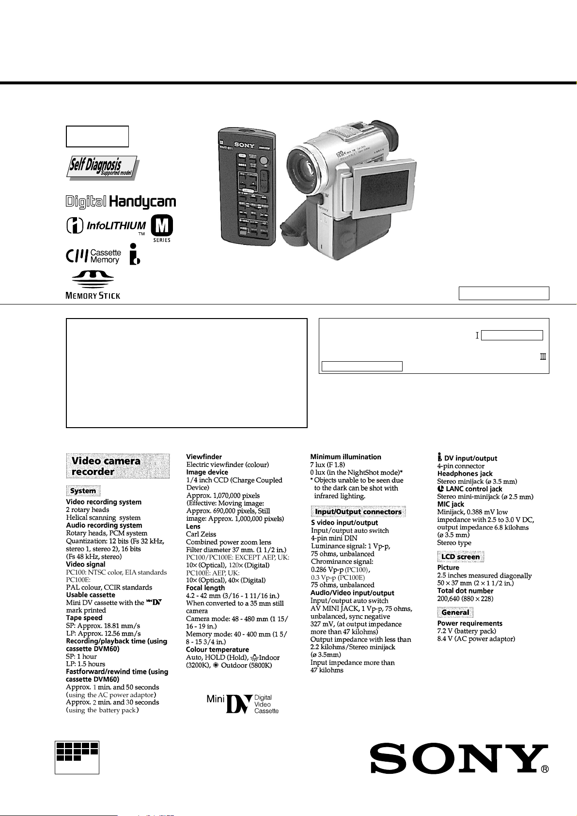
Photo : DCR-PC100
On the VC-227 board
This service manual provides the information that is premised
the circuit board replacement service and not intended repair
inside the VC-227 board.
Therefore, schematic diagram, printed wiring board and
electriacal parts list of the VC-227 board are not shown.
The following pages are not shown.
Schematic diagram .......................... Pages 4-13 to 4-42
Printed wiring board......................... Pages 4-43 to 4-46
Electrical parts list............................ Pages 6-18 to 6-25
US Model
Canadian Model
Korea Model
DCR-PC100
AEP Model
UK Model
Australian Model
Chinese Model
DCR-PC100E
E Model
Hong Kong Model
Tourist Model
DCR-PC100/PC100E
D300 MECHANISM
For MECHANISM ADJUSTMENTS, refer to the “DV
MECHANICAL ADJUSTMENT MANUAL
(original: 9-973-815-11, supplement: 9-973-815-81)
and “DV MECHANICAL ADJUSTMENT MANUAL
D200 MECHANISM ” (original: 9-973-981-11).
DCR-PC100 : NTSC model
DCR-PC100E : PAL model
D MECHANISM”
SPECIFICATIONS
— Continued on next page —
DIGITAL VIDEO CAMERA RECORDER
MICROFILM
Page 2
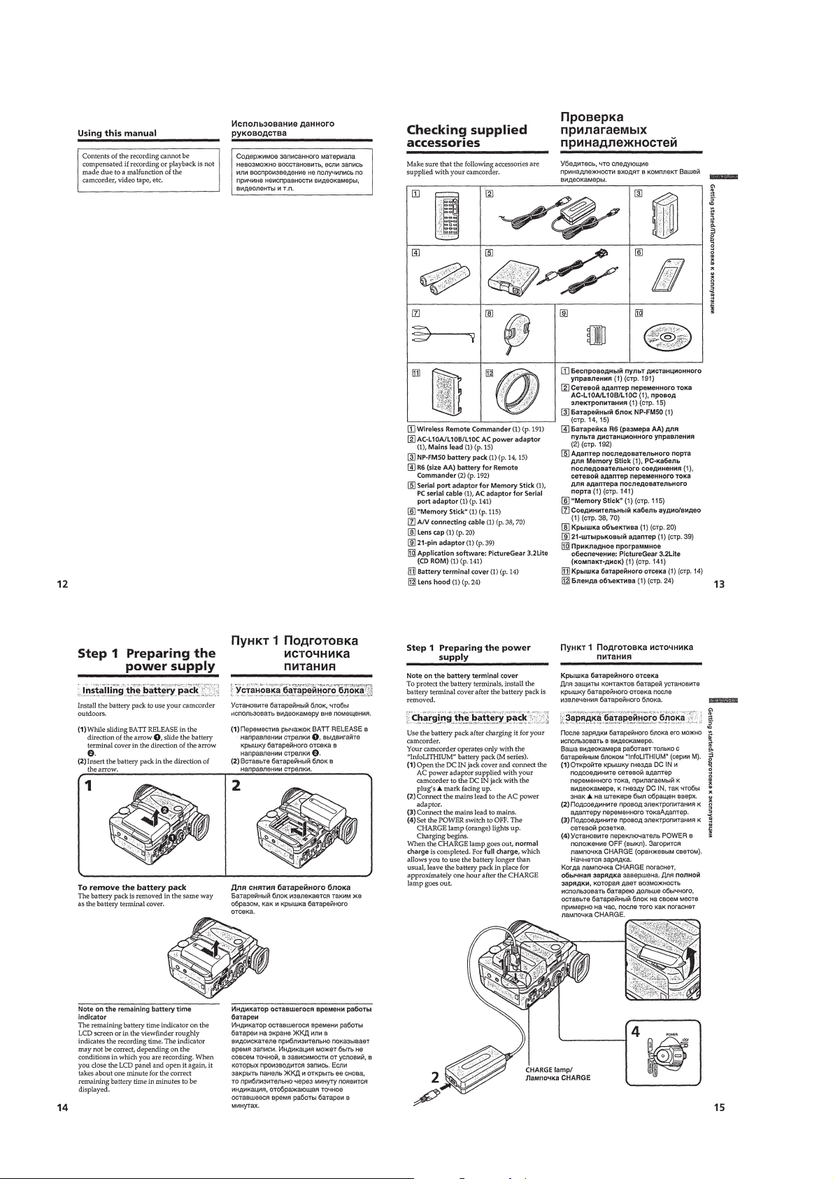
• SUPPLIED ACCESSORIES
Check that the following accessories are supplied with your
camcorder.
• DIFFERENCE TABLE
Model
Color System
Lens
COMPONENTS IDENTIFIED BY MARK ! OR DO TTED LINE WITH
MARK ! ON THE SCHEMATIC DIAGRAMS AND IN THE PARTS
LIST ARE CRITICAL TO SAFE OPERATION. REPLACE THESE
COMPONENTS WITH SONY PARTS WHOSE PART NUMBERS
APPEAR AS SHOWN IN THIS MANUAL OR IN SUPPLEMENTS
PUBLISHED BY SONY.
Optical
Digital
SAFETY-RELATED COMPONENT WARNING!!
DCR-PC100
NTSC
10 ×
120 ×
DCR-PC100E
PAL
10 ×
120 ×, 40 × *
*: AEP, UK model
SAFETY CHECK-OUT
After correcting the original service problem, perform the following
safety checks before releasing the set to the customer.
1. Check the area of your repair for unsoldered or poorly-soldered
connections. Check the entire board surface for solder splashes
and bridges.
2. Check the interboard wiring to ensure that no wires are
"pinched" or contact high-wattage resistors.
3. Look for unauthorized replacement parts, particularly
transistors, that were installed during a previous repair . Point
them out to the customer and recommend their replacement.
• Abbreviation
AUS: Australian model
JE: Tourist model
CND: Canadian model
CN: Chinese model
HK: Hong Kong model
KR: Korea model
ATTENTION AU COMPOSANT AYANT RAPPORT
À LA SÉCURITÉ!
LES COMPOSANTS IDENTIFÉS P AR UNE MARQUE ! SUR LES
DIAGRAMMES SCHÉMA TIQUES ET LA LISTE DES PIÈCES SONT
CRITIQUES POUR LA SÉCURITÉ DE FONCTIONNEMENT. NE
REMPLACER CES COMPOSANTS QUE PAR DES PIÈSES SONY
DONT LES NUMÉROS SONT DONNÉS DANS CE MANUEL OU
DANS LES SUPPÉMENTS PUBLIÉS PAR SONY.
4. Look for parts which, through functioning, show obvious signs
of deterioration. Point them out to the customer and
recommend their replacement.
5. Check the B+ voltage to see it is at the values specified.
6. Flexible Circuit Board Repairing
• Keep the temperature of the soldering iron around 270˚C
during repairing.
• Do not touch the soldering iron on the same conductor of the
circuit board (within 3 times).
• Be careful not to apply force on the conductor when soldering
or unsoldering.
— 2 —
Page 3

TABLE OF CONTENTS
SERVICE NOTE
1. POWER SUPPLY DURING REPAIRS ····························· 6
2. TO TAKE OUT A CASSETTE WHEN NOT EJECT
(FORCE EJECT) ································································6
SELF-DIAGNOSIS FUNCTION
1. SELF-DIAGNOSIS FUNCTION······································· 7
2. SELF-DIAGNOSIS DISPLAY ·········································· 7
3. SERVICE MODE DISPLAY ············································· 7
3-1. Display Method ··································································7
3-2. Switching of Backup No. ··················································· 7
3-3. End of Display···································································· 7
4. SELF-DIAGNOSIS CODE TABLE··································· 8
1. GENERAL
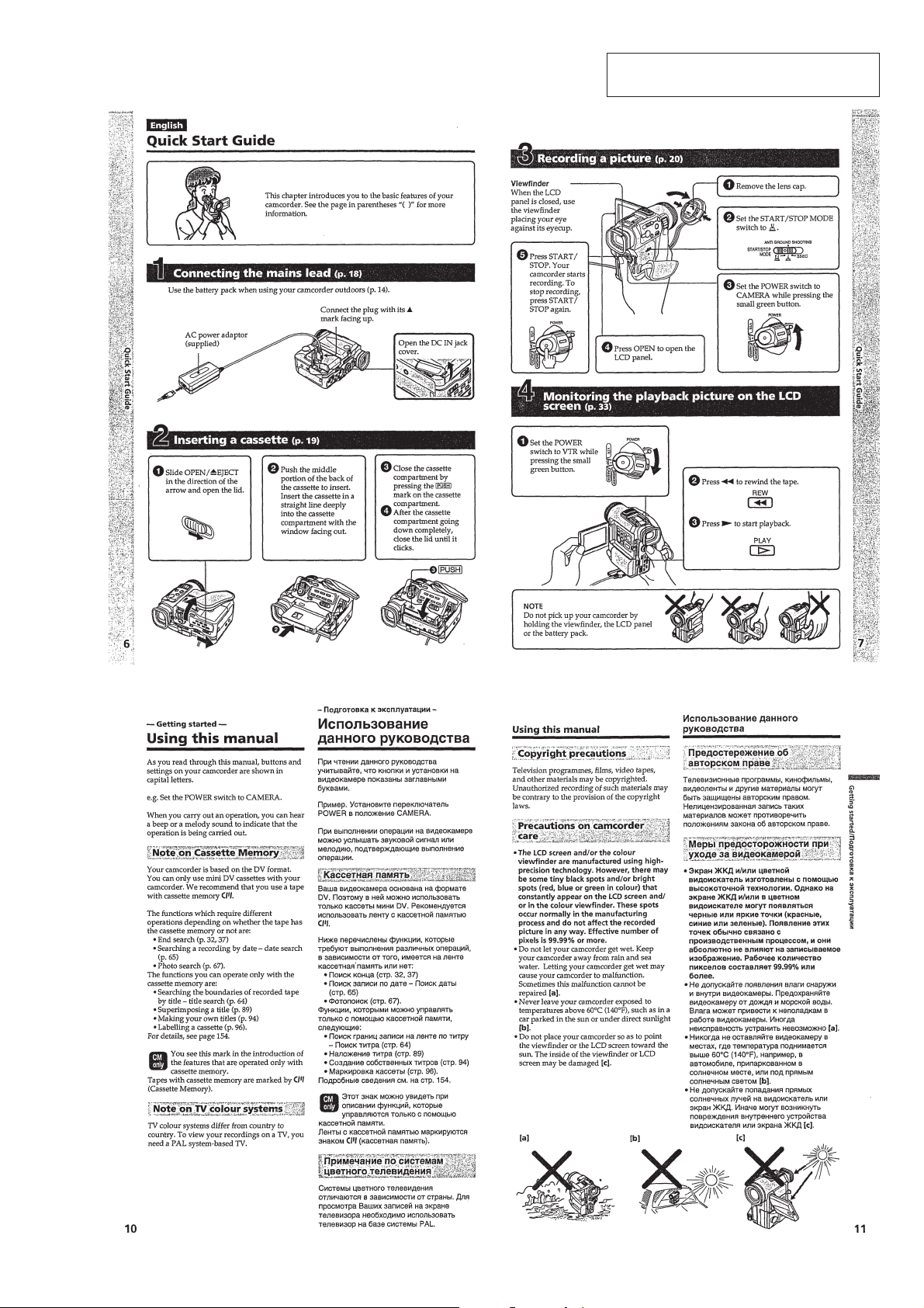
Quick Start Guide ······································································1-1
Getting started ···········································································1-1
Using this manual ··································································1-1
Checking supplied accessories ··············································1-2
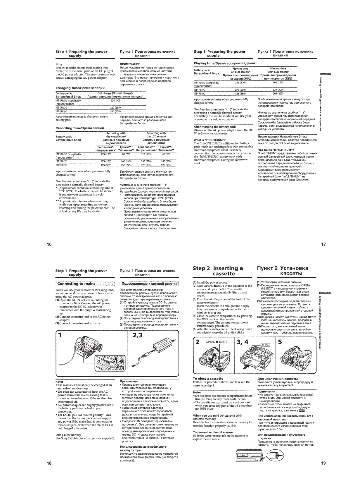
Step 1 Preparing the power supply ········································1-2
Installing the battery pack····················································1-2
Charging the battery pack ····················································1-2
Connecting to mains ····························································1-3
Step 2 Inserting a cassette······················································1-3
Recording –Basics ·····································································1-4
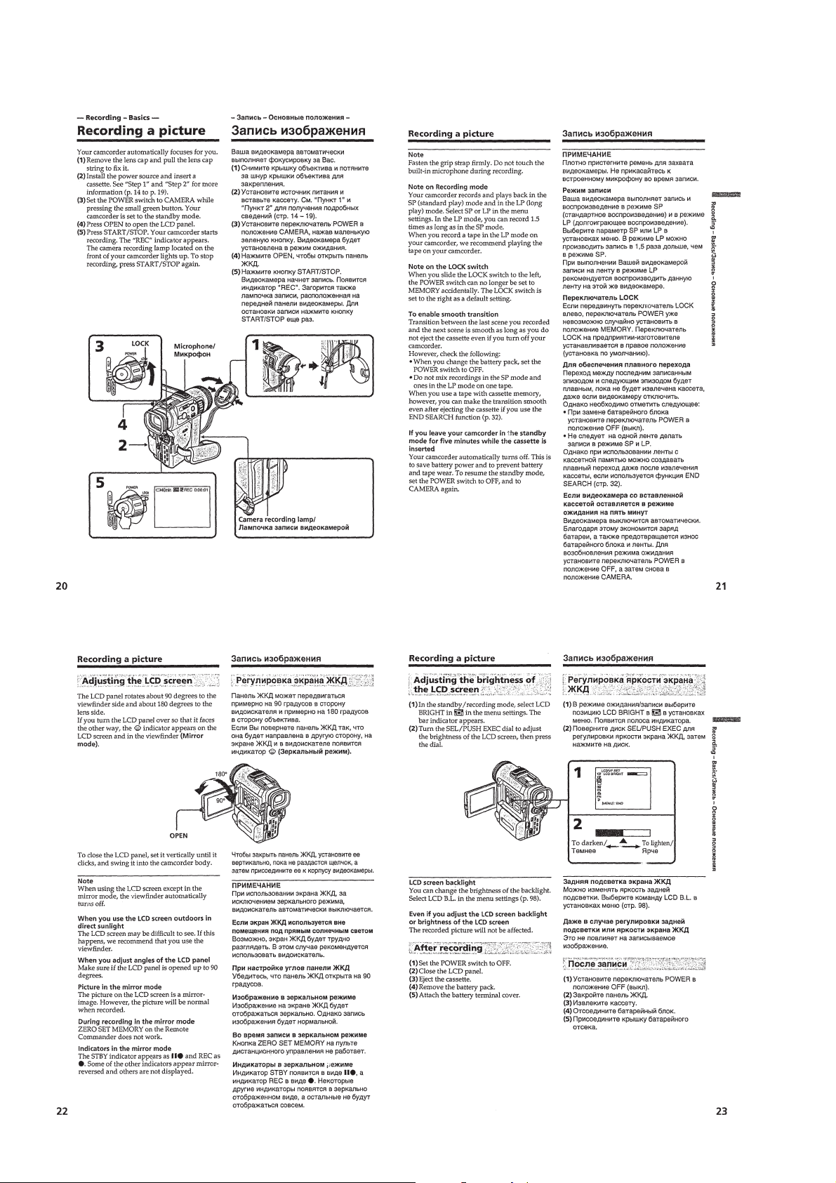
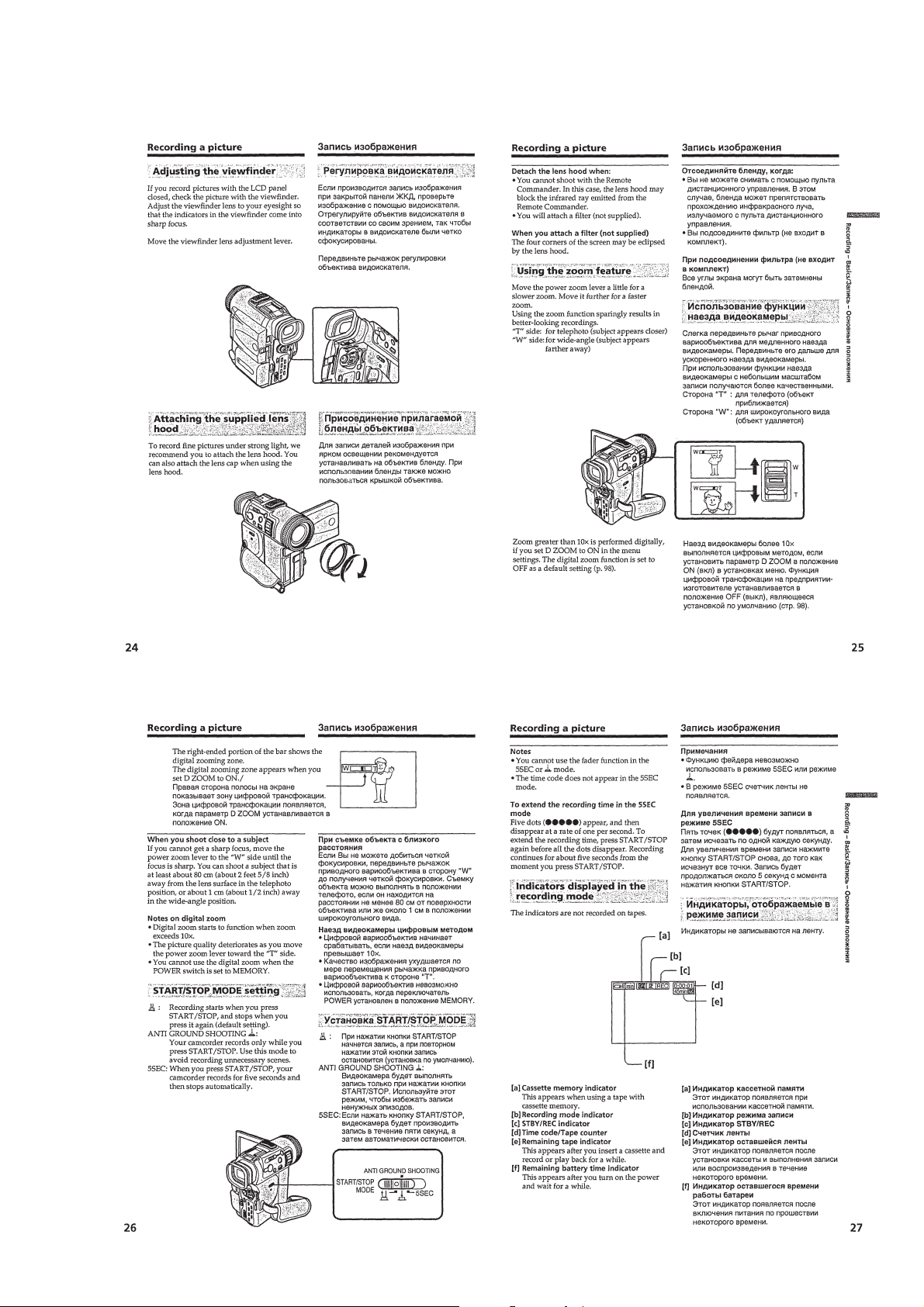
Recording a picture································································ 1-4
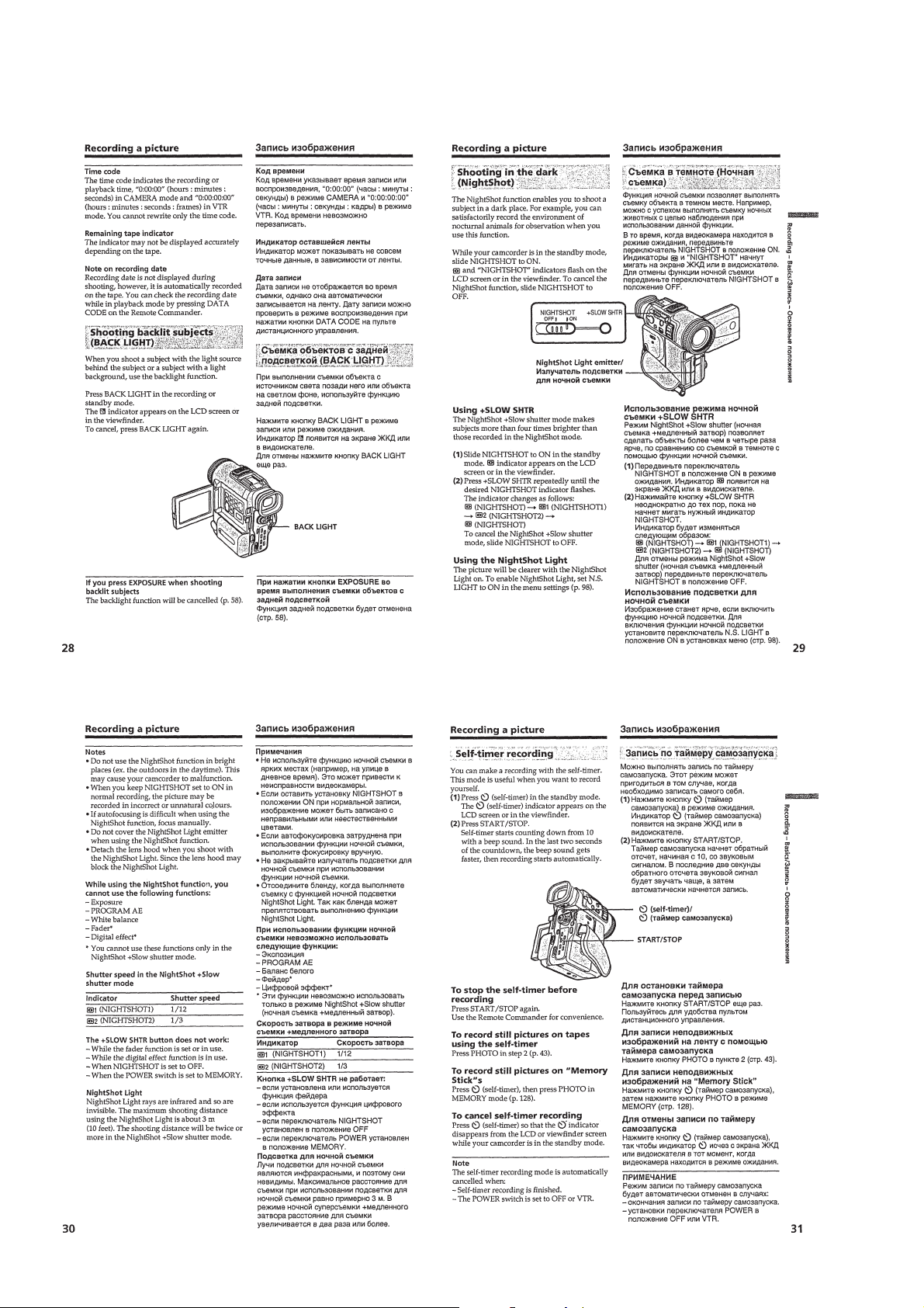
Shooting backlit subjects (BACK LIGHT)··························1-6
Shooting in the dark (NightShot)·········································1-6
Self-timer recording····························································· 1-6
END SEARCH ····································································1-7
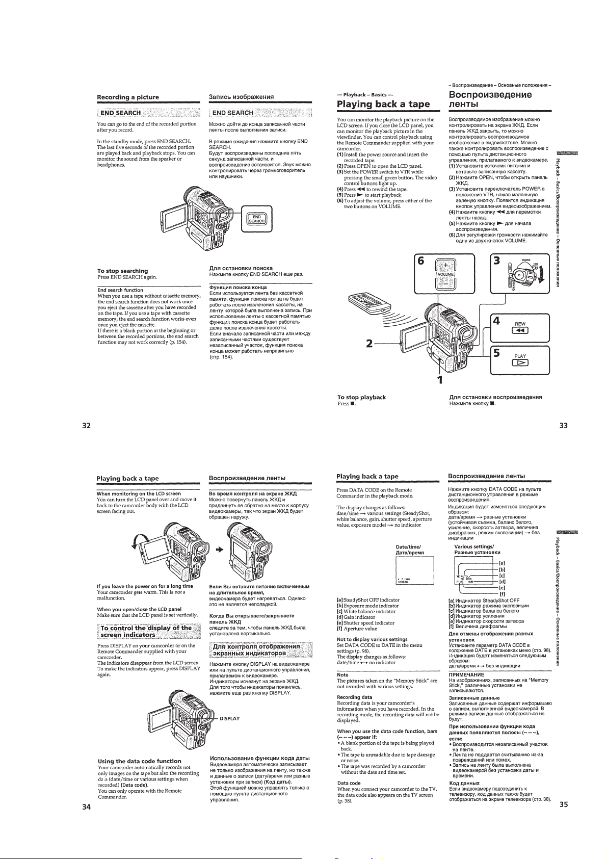
Playback –Basics ·······································································1-7
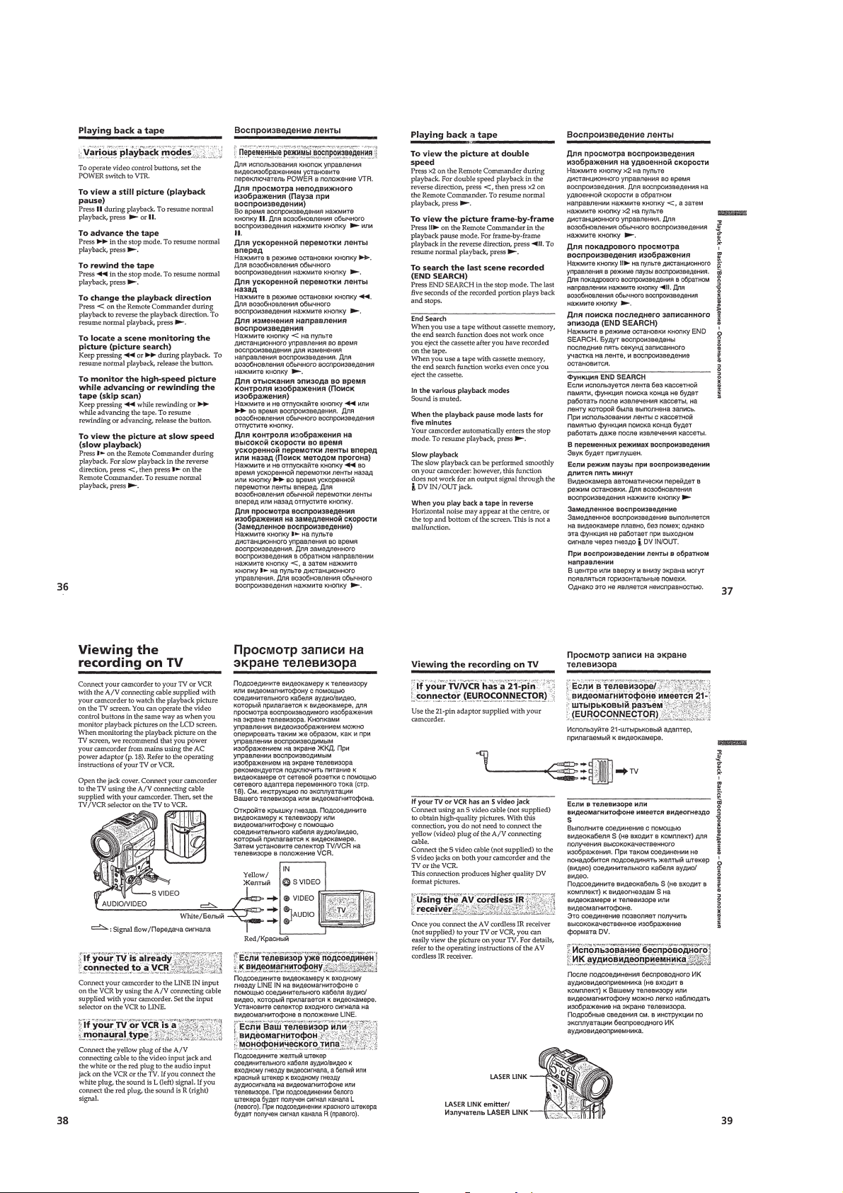
Playing back a tape ································································1-7
Viewing the recording on TV ················································1-8
Advanced Recording Operations···············································1-9
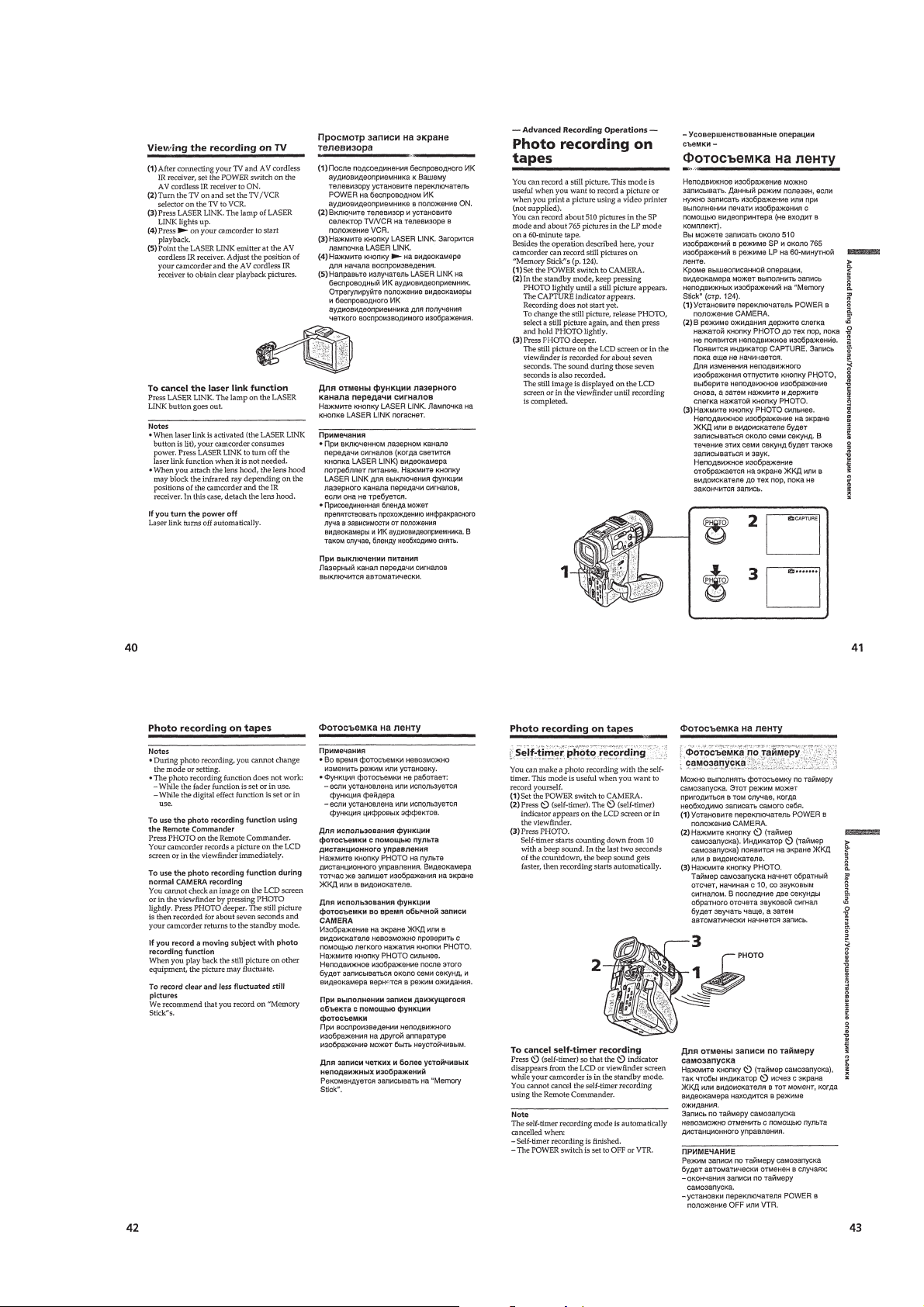
Photo recording on tapes ·······················································1-9
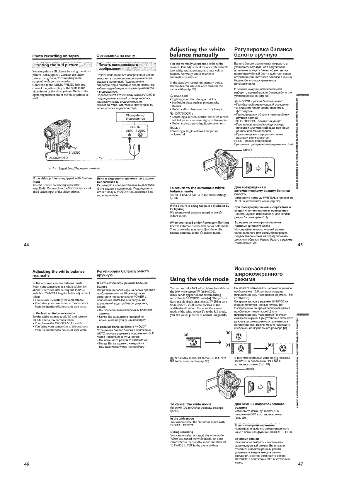
Adjusting the white balance manually·································1-10
Using the wide mode ···························································1-10
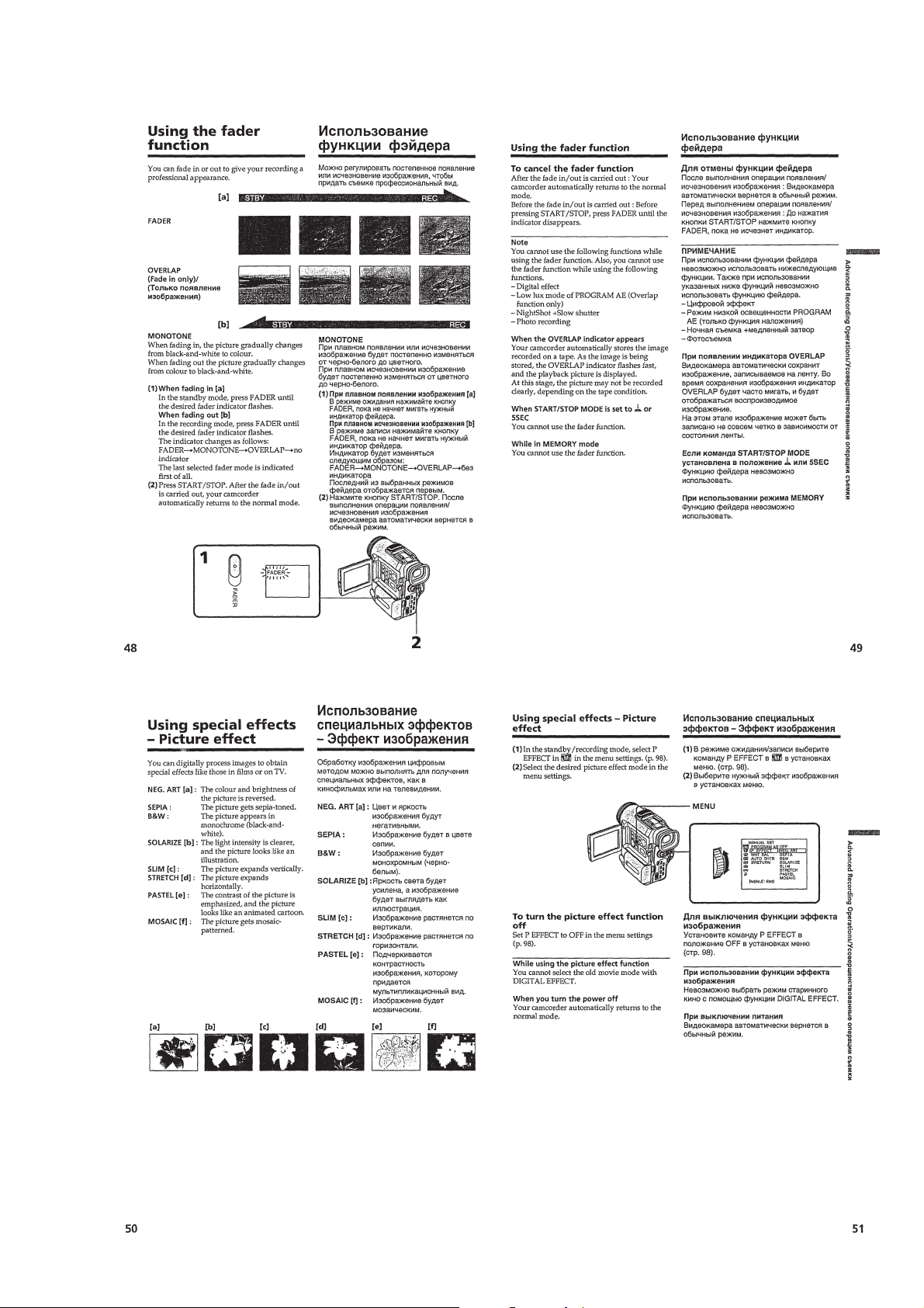
Using the fader function ······················································ 1-11
Using special effects –Picture effect····································1-11
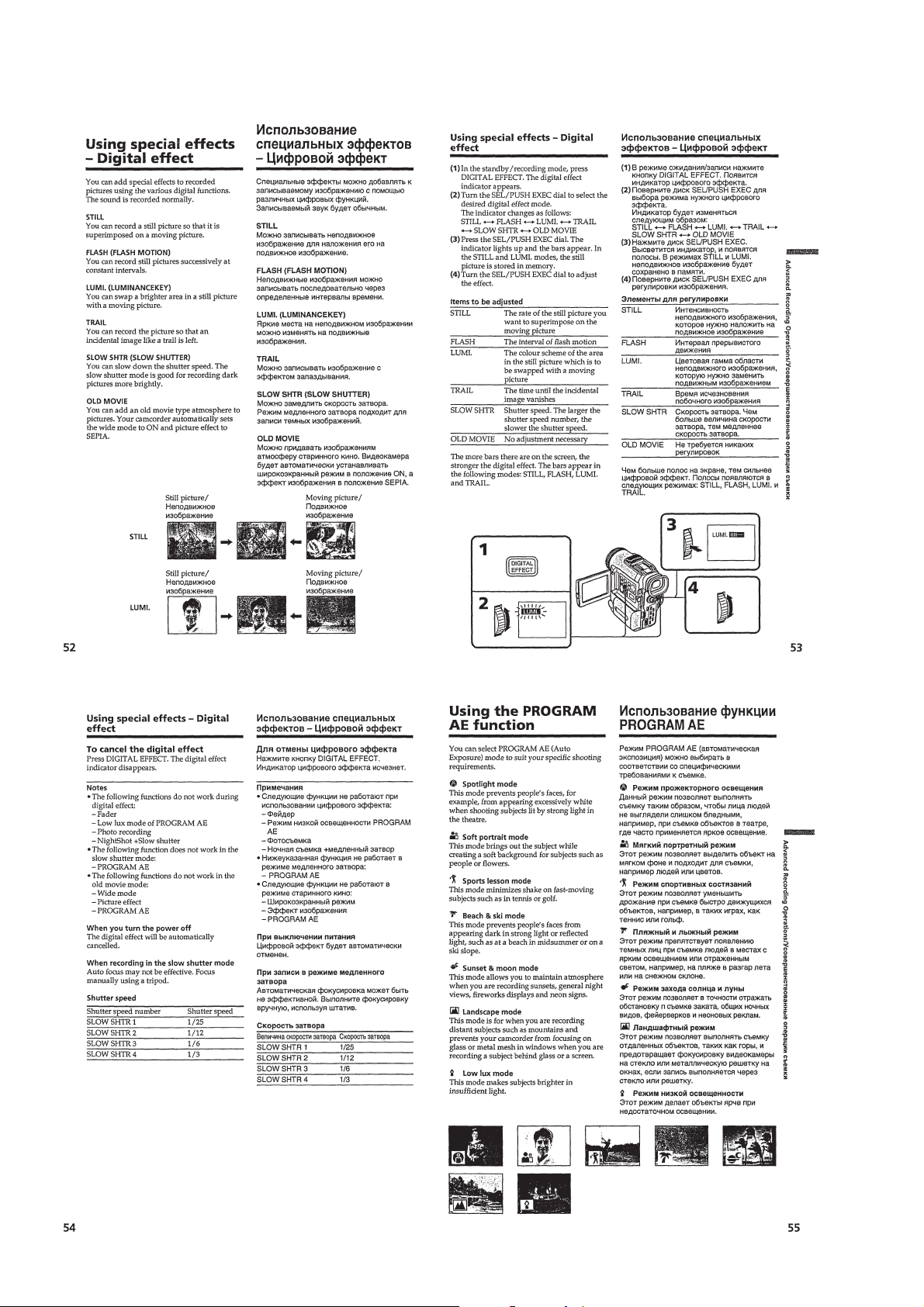
Using special effects –Digital effect····································1-12
Using the PROGRAM AE function ·····································1-12
Adjusting the exposure manually ········································ 1-13
Focusing manually······························································· 1-13
Advanced Playback Operations···············································1-14
Playing back a tape with picture effects ······························1-14
Playing back a tape with digital effects ·······························1-14
Quickly locating a scene using the zero set memory
function ················································································1-14
Searching the boundaries of recorded tape by title
–Title search·········································································1-15
Searching a recording by date –Date search························1-15
Searching for a photo-Photo search/Photo scan ··················1-15
Editing ·····················································································1-16
Dubbing a tape ·····································································1-16
Editing partially on a DV tape –DV synchro-editing ··········1-17
Recording video or TV programmes ···································1-18
Inserting a scene from a VCR –Insert editing······················1-19
Audio dubbing ·····································································1-20
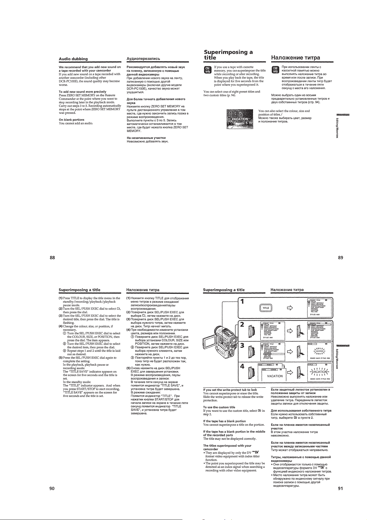
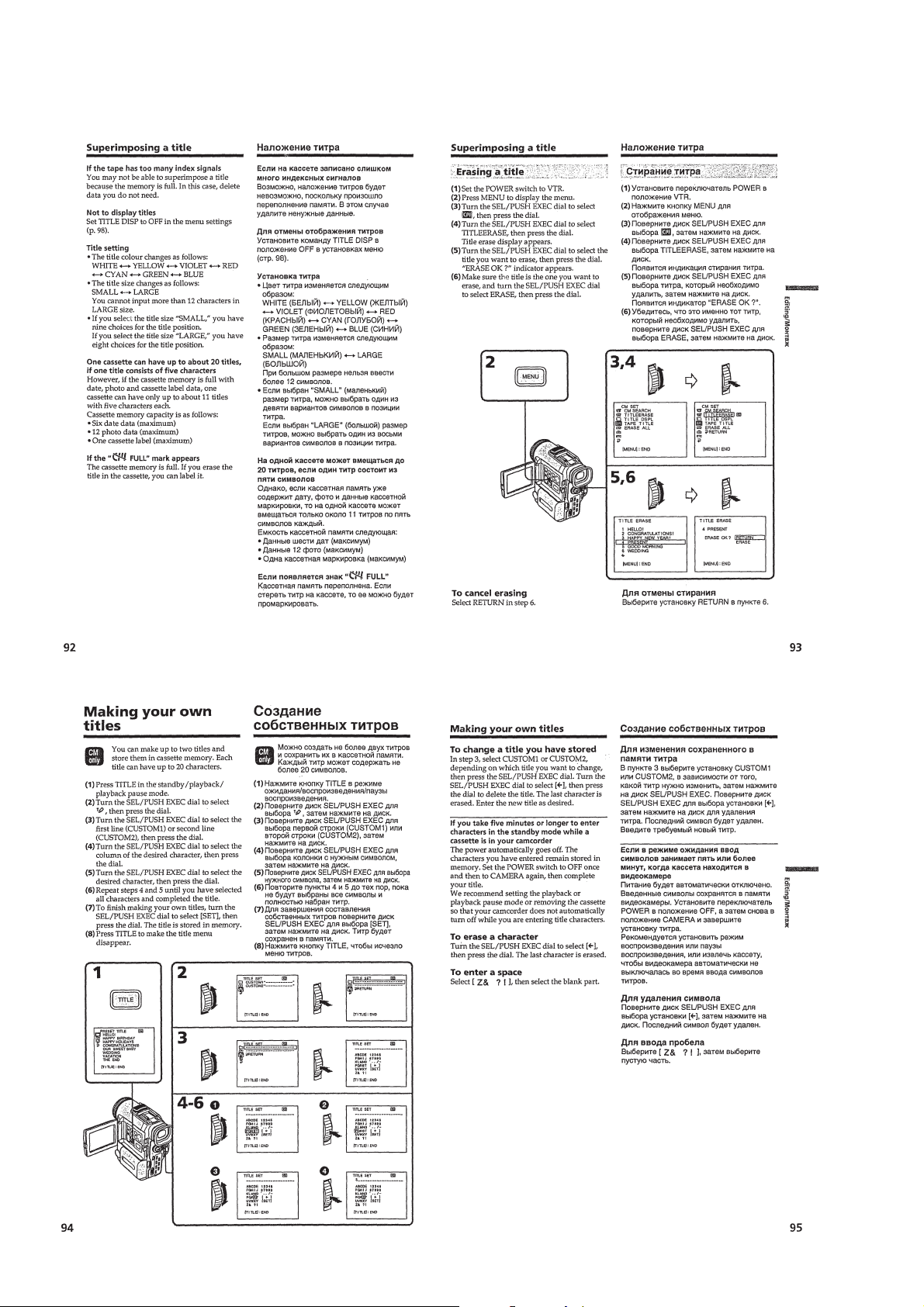
Superimposing a title ··························································· 1-21
Making your own titles ························································1-22
Labeling a cassette ·······························································1-23
Customizing Y our Camcorder ·················································1-23
Changing the menu settings················································· 1-23
Resetting the date and time·················································· 1-25
“Memory Stick” Operations ····················································1-26
Using a “Memory Stick” –introduction ·······························1-26
Recording still images on “Memory Stick”s
–Memory photo recording ···················································1-28
Superimposing a still picture in a “Memory Stick”
on a moving picture –MEMORY MIX································1-29
Recording an image from a mini DV tape as a still image ··1-30
Copying still images from a mini DV tape –Photo save ······1-31
Viewing a still picture –Memory photo playback················1-31
Copying the image recorded on “Memory Stick”s to
mini DV tapes ······································································1-32
Playing back images continuously –SLIDE SHOW·············· 1-33
Preventing accidental erasure –Image protection ················1-33
Deleting images ···································································1-34
Writing a print mark –PRINT MARK·································1-35
Additional Information ····························································1-35
Usable cassettes ···································································1-35
Troubleshooting ···································································1-36
Self-diagnosis display ··························································1-38
Warning indicators and messages ········································1-38
Using your camcorder abroad··············································1-38
Maintenance information and precautions···························1-39
Quick Reference ······································································1-40
Identifying the parts and controls ········································1-40
Quick Function Guide ·························································1-43
2. DISASSEMBLY
2-1. LCD UNIT, PD-125 BOARD ·········································2-2
2-2. MD BLOCK-1·································································2-3
2-3. MR-44 BOARD, MD BLOCK-2 ····································2-4
2-4. LENS ASSEMBLY, EVF BLOCK ASSEMBLY,
CONTROL SWITCH BLOCK (ME-4950) ····················2-5
2-5. VC-227 (VC-227P) BOARD, SPEAKER, MEMORY
STICK CONNECTOR, MICROPHONE UNIT,
MA-367 BOARD ····························································2-5
2-6. HINGE ASSEMBL Y·······················································2-6
2-7. DC-IN CONNECTOR, BATTERY TERMINAL BOARD,
FJ-25 BOARD ·································································2-6
2-8. CCD/CD BLOCK ASSEMBLY, MF RING BLOCK
ASSEMBLY ···································································· 2-8
2-9. VF-138 BOARD, VF HOLDER ASSEMBLY,
EYE CUP ASSEMBLY···················································2-8
2-10. CONTROL SWITCH BLOCK (FK-4950) ····················· 2-9
2-11. CIRCUIT BOARDS LOCATION ································· 2-10
2-12. FLEXIBLE BOARDS LOCATION ······························2-11
3. BLOCK DIAGRAMS
3-1. OVERALL BLOCK DIAGRAM-1·································3-1
OVERALL BLOCK DIAGRAM-2·································3-3
OVERALL BLOCK DIAGRAM-3·································3-5
3-2. POWER BLOCK DIAGRAM-1 ·····································3-7
POWER BLOCK DIAGRAM-2 ·····································3-9
4. PRINTED WIRING BOARDS AND
SCHEMATIC DIAGRAMS
4-1. FRAME SCHEMATIC DIAGRAM-1 ···························· 4-1
FRAME SCHEMATIC DIAGRAM-2 ····························4-3
4-2. PRINTED WIRING BOARDS AND
SCHEMATIC DIAGRAMS ············································4-5
• CD-234 (CCD IMAGER)
PRINTED WIRING BOARD ·························4-7
• CD-234 (CCD IMAGER)
SCHEMATIC DIAGRAM ····························4-11
Shematic diagram and printed wiring board of the
VC-227 board are not shown.
Pages from 4-13 to 4-46 are not shown.
— 3 —
Page 4

• MR-44 (CONNECTOR, DRUM/CAPSTAN MOTOR
DRIVE, TIMING GENERATOR, REC/PB HEAD AMP,
LASER LINK)
PRINTED WIRING BOARD ·······················4-47
• FP-91 (MODE), FP-92 (TOP/END SENSOR,
TAPE LED), FP-242 (S/T REEL SENSOR)
PRINTED WIRING BOARDS ·····················4-49
• MR-44 (CONNECTOR)(1/5)
SCHEMATIC DIAGRAM ····························4-51
• MR-44 (DRUM/CAPSTAN MOTOR DRIVE)(2/5)
SCHEMATIC DIAGRAM ····························4-53
• MR-44 (ID DETECT, TIMING GENERATOR)(3/5)
SCHEMATIC DIAGRAM ····························4-55
• MR-44 (REC/PB HEAD AMP)(4/5)
SCHEMATIC DIAGRAM ····························4-57
• MR-44 (LASER LINK)(5/5)
SCHEMATIC DIAGRAM ····························4-59
• FJ-25 (VIDEO IN/OUT, DC IN)
SCHEMATIC DIAGRAM ····························4-61
• FJ-25 (VIDEO IN/OUT, DC IN)
PRINTED WIRING BOARD ·······················4-63
• CONTROL SWITCH BLOCK (FK-4950)
SCHEMATIC DIAGRAM ····························4-67
• CONTROL SWITCH BLOCK (ME-4950)
SCHEMATIC DIAGRAM ····························4-69
• MA-367 (MIC AMP)
PRINTED WIRING BOARD ·······················4-71
• MA-367 (MIC AMP)
SCHEMATIC DIAGRAM ····························4-73
• PD-125 (RGB DRIVER, TG)
PRINTED WIRING BOARD ·······················4-75
• PD-125 (RGB DRIVER)(1/2)
SCHEMATIC DIAGRAM ····························4-77
• PD-125 (TG)(2/2)
SCHEMATIC DIAGRAM ····························4-79
• VF-138 (LCD DRIVER)(1/2)
SCHEMATIC DIAGRAM ····························4-81
• VF-138 (BACK LIGHT DRIVER)(2/2)
SCHEMATIC DIAGRAM ····························4-83
• VF-138 (LCD DRIVER, BACK LIGHT DRIVER)
PRINTED WIRING BOARD ·······················4-85
4-3. WAVEFORMS ······························································4-87
4-4. MOUNTED LOCATION ··············································4-92
5 ADJUSTMENTS
1. Before starting adjustment···············································5-1
1-1. Adjusting items when replacing main parts and boards.·5-2
5-1. CAMERA SECTION ADJUSTMENT ···························5-4
1-1. PREPARATIONS BEFORE ADJUSTMENT
(CAMERA SECTION) ···················································5-4
1-1-1.List of Service Tools ························································5-4
1-1-2.Preparations ·····································································5-5
1-1-3.Precaution ········································································5-7
1. Setting the Switch····························································5-7
2. Order of Adjustments ······················································5-7
3. Subjects ···········································································5-7
1-2. INITIALIZATION OF B, C, D, E, F, 7 PAGE DATA·····5-8
1-2-1.INITIALIZATION OF C PAGE DATA···························5-8
1. Initializing the C Page Data·············································5-8
2. Modification of C Page Data··········································· 5-8
3. C Page Table ····································································5-8
1-2-2.INITIALIZATION OF D PAGE DATA ························5-10
1. Initializing the D Page Data ··········································5-10
2. Modification of D Page Data·········································5-10
3. D Page Table··································································5-11
1-2-3.INITIALIZATION OF B PAGE DATA·························5-12
1. Initializing the B Page Data···········································5-12
2. Modification of B Page Data·········································5-12
3. B Page Table ··································································5-13
1-2-4.INITIALIZATION OF E, F, 7 PAGE DATA ·················5-13
1. Initializing the E, F, 7 Page Data ···································5-13
2. Modification of E, F, 7 Page Data ·································5-13
3. Modification of F Page Data ·········································5-14
4. F Page Table ··································································5-14
5. E Page Table ··································································5-17
6. 7 Page Table···································································5-19
1-3. CAMERA SYSTEM ADJUSTMENTS ························5-21
1. 54MHz/66MHz Origin Oscillation Adjustment
(CD-234 board) ·····························································5-21
2. Zoom Key Center Adjustment ·······································5-21
3. HALL Adjustment ·························································5-22
4. MR Adjustment ·····························································5-22
5. Flange Back Adjustment (Using Minipattern Box)·······5-23
6. Flange Back Adjustment
(Using Flange Back Adjustment Chart and Subject
More Than 500m Away)···············································5-24
6-1. Flange Back Adjustment (1)··········································5-24
6-2. Flange Back Adjustment (2)··········································5-24
7. Flange Back Check························································5-25
8. Picture Frame Setting ····················································5-25
9. Color Reproduction Adjustment····································5-26
10. MAX GAIN Adjustment ···············································5-27
11. Auto White Balance & LV Standard Data Input ···········5-27
12. Auto White Balance Adjustment ···································5-28
13. White Balance Check ····················································5-28
14. Mechanical Shutter Data Input······································5-29
15. Angular Velocity Sensor Sensitivity Adjustment ··········5-29
1-4. COLOR ELECTRONIC VIEWFINDER
SYSTEM ADJUSTMENT ············································5-30
1. VCO Adjustment (VF-138 board)·································5-30
2. Bright Adjustment (VF-138 board) ·······························5-31
3. Contrast Adjustment (VF-138 board)····························5-31
4. White Balance Adjustment (VF-138 board)··················5-32
1-5. LCD SYSTEM ADJUSTMENT ···································5-33
1. VCO Adjustment (PD-125 board)·································5-33
2. Black Limit Adjustment (PD-125 board) ······················5-34
3. Bright Adjustment (PD-125 board) ·······························5-34
4. Gamma-1 Adjustment (PD-125 board) ·························5-35
5. Contrast Adjustment (PD-125 board)····························5-35
6. Center Level Adjustment (PD-125 board) ·····················5-36
7. White Balance Adjustment (PD-125 board)··················5-36
5-2. MECHANISM SECTION ADJUSTMENT··················5-37
2-1. HOW TO ENTER RECORD MODE WITHOUT
CASSETTE ···································································5-37
2-2. HOW TO ENTER PLAYBACK MODE
WITHOUT CASSETTE················································5-37
2-3. TAPE PATH ADJUSTMENT········································5-37
1. Preparation for Adjustment ···········································5-37
2. Processing after Completing Operations:······················5-37
5-3. VIDEO SECTION ADJUSTMENT······························5-38
3-1. PREPARATIONS BEFORE ADJUSTMENTS ············5-38
3-1-1.Equipment to Required··················································5-38
3-1-2.Precautions on Adjusting···············································5-39
3-1-3.Adjusting Connectors ····················································5-40
3-1-4.Connecting the Equipment ············································5-40
3-1-5.Checking the Input Signals············································5-40
3-1-6.Alignment Ta pes····························································5-41
3-1-7.Input/Output Level and Impedance ·······························5-41
3-2. SYSTEM CONTROL SYSTEM ADJUSTMENT········5-42
1. Initialization of B, C, D, E, F, 7 Page Data ···················5-42
2. Serial No. Input ·····························································5-42
2-1. Company ID Input·························································5-42
2-2. Serial No. Input ·····························································5-42
3. Battery End Check (VC-227 board) ······························5-44
— 4 —
Page 5

3-3. SERVO AND RF SYSTEM ADJUSTMENT ··············· 5-45
1. Cap FG Duty Adjustment (VC-227 board) ···················5-45
2. T reel FG Duty Adjustment (VC-227 board) ·············· -5-45
3. PLL f0 & LPF f0 Adjustment (VC-227 board)···············5-45
4. Switching Position Adjustment (VC-227 board)··········· 5-46
5. AGC Center Level and APC & AEQ Adjustment ·········5-46
5-1. Preparations before adjustments····································5-46
5-2. AGC Center Level Adjustment (VC-227 board) ···········5-46
5-3. APC & AEQ Adjustment (VC-227 board) ····················5-47
5-4. Processing after Completing Adjustments ····················5-47
6. PLL f0 & LPF f0 Final Adjustment (VC-227 board)······5-47
3-4. VIDEO SYSTEM ADJUSTMENTS·····························5-48
3-4-1.Base Band Block Adjustments ······································ 5-48
1. Chroma BPF f0 Adjustment (VC-227 Board)················5-48
2. S VIDEO OUT Y Level Adjustment (VC-227 Board) ·· 5-48
3. S VIDEO OUT Chroma Level Adjustment
(VC-227 Board)·····························································5-49
4. AV OUT Y, Chroma Level Check (VC-227 Board) ······5-49
5. PLL Adjustment (VC-227 Board) ·································5-50
3-4-2.BIST Check ···································································5-51
1. Playback System Check ················································ 5-51
1-1. Preparation for Playback ··············································· 5-51
1-2. IC1900(TRX) BIST(PB) Check····································5-51
1-3. IC1601(TFD) BIST(PB) Check ····································5-51
1-4. IC1600(SFD) BIST(PB) Check····································· 5-51
1-5. IC1501(VFD) BIST(PB) Check····································5-52
2. Recording System Check ·············································· 5-53
2-1. Preparations for recording·············································5-53
2-2. IC1501(VFD) BIST(REC) Check·································5-53
2-3. IC1600(SFD) BIST(REC) Check··································5-53
2-4. IC1601(TFD) BIST(REC) Check ·································5-54
2-5. IC1900(TRX) BIST(REC) Check·································5-54
3-5. IR TRANSMITTER ADJUSTMENTS ·························5-55
1. IR Video Carrier Frequency Adjustment
(MR-44 board)·······························································5-55
2. IR Video Deviation Adjustment (MR-44 board) ··········· 5-55
3. IR Audio Deviation Adjustment (MR-44 board)···········5-56
3-6. AUDIO SYSTEM ADJUSTMENTS ····························5-57
1. Playback Level Check ··················································· 5-58
2. Overall Level Characteristics Check ·····························5-58
3. Overall Distortion Check···············································5-58
4. Overall Noise Level Check············································5-58
5. Overall Separation Check·············································· 5-58
5-4. SERVICE MODE··························································5-59
4-1. ADJUSTMENT REMOTE COMMANDER ················5-59
1. Using the adjustment remote commander ····················· 5-59
2. Precautions upon using the adjustment
remote commander ························································ 5-59
4-2. DATA PROCESS··························································· 5-60
4-3. SERVICE MODE··························································5-61
1. Setting the Test Mode ···················································· 5-61
2. Emergence Memory Address ········································5-61
2-1. EMG Code (Emergency Code) ·····································5-61
2-2. MSW Code····································································5-62
3. Bit value discrimination ················································ 5-63
4. Switch check (1) ····························································5-63
5. Switch check (2) ····························································5-64
6. Record of Use check······················································5-64
6-1-6.CASSETTE COMPARTMENT AND DRUM ASSY
SECTION ········································································ 6-6
6-1-7.LS CHASSIS SECTION ·················································6-7
6-1-8.MECHANISM CHASSIS BLOCK SECTION-1 ··········· 6-8
6-1-9.MECHANISM CHASSIS BLOCK SECTION-2 ··········· 6-9
6-2. ELECTRICAL PARTS LIST ········································ 6-10
Parts list of the VC-227 board is not shown.
Pages from 6-18 to 6-25 are not shown.
* Parts reference sheet and color reproduction frame are
shown on page 226 and 227.
6. REPAIR PARTS LIST
6-1. EXPLODED VIEWS ······················································6-1
6-1-1.CABINET (R) SECTION-1 ············································6-1
6-1-2.CABINET (R) SECTION-2 ············································6-2
6-1-3.CABINET (R) SECTION-3 ············································6-3
6-1-4.CABINET (L) BLOCK ASSEMBLY ·····························6-4
6-1-5.LENS ASSEMBLY, EVF BLOCK ASSEMBLY ············ 6-5
— 5 —
Page 6
SERVICE NOTE
1. POWER SUPPLY DURING REPAIRS
In this unit, about 10 seconds after power is supplied to the battery
terminal using the regulated power supply (8.4 V), the power is
shut off so that the unit cannot operate.
This following two methods are av ailable to prev ent this. Take note
of which to use during repairs.
Method 1.
Connect the servicing remote commander RM-95 (J-6082-053-B)
to the LANC jack, and set the commander switch to the “ADJ”
side.
Method 2.
Use the DC IN terminal. (Use the A C po wer adaptor (A C-L10, A CVQ800 etc. ))
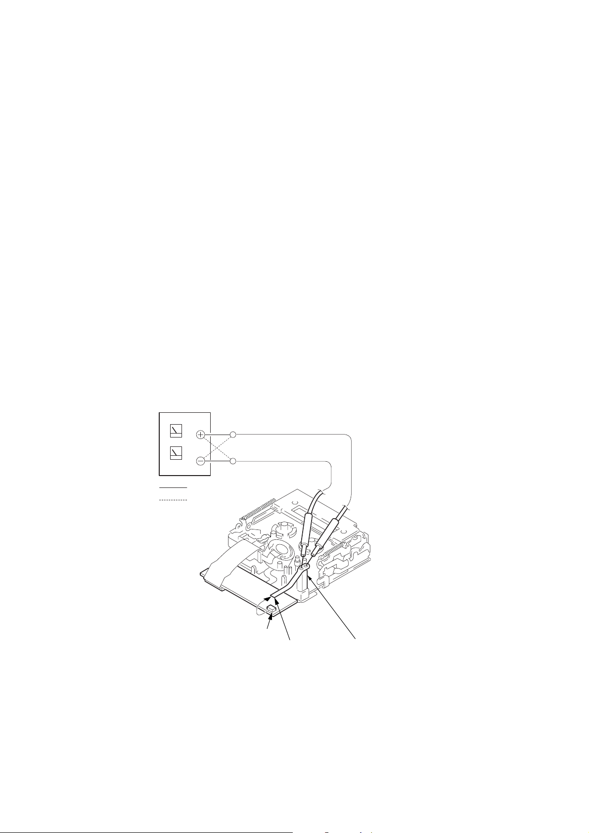
2. TO TAKE OUT A CASSETTE WHEN
NOT EJECT (FORCE EJECT)
1 Refer to 2-2 to remove the shoe cover.
2 Refer to 2-3. to remove the cabinet (L) assembly.
3 Refer to 2-3. to remove the mechanism deck.
4 Disconnect from CN2303 (4P, 0.8mm) of MR-44 board.
5 Add +4.5 V from the DC PO WER SUPPLY and unload with a
pressing the cassette compartment.
DC power supply
(+4.5Vdc)
: Unloading
: Loading
MR-44
BOARD
CN2303
Disconnect from CN2303 (4P)
of MR-44 board.
Loading motor
— 6 —
Page 7
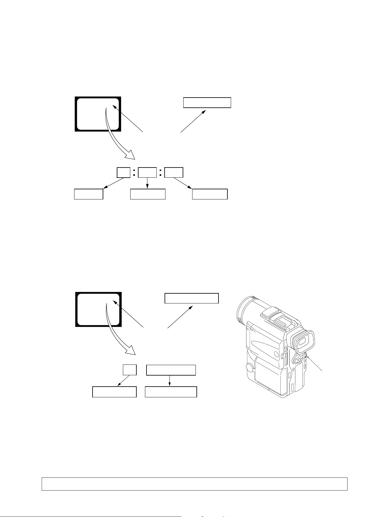
SELF-DIAGNOSIS FUNCTION
1. SELF-DIAGNOSIS FUNCTION
When problems occur while the unit is operating, the self-diagnosis
function starts working, and displays on the viewf inder, LCD screen
or LCD window what to do. This function consists of two display;
self-diagnosis display and service mode display.
Details of the self-diagnosis functions are provided in the Instruction
manual.
Viewfinder or LCD screen LCD window
C : 3 1 : 1 1
Blinks at 3.2Hz
1 1
Repaired by:
C : Corrected by customer
H : Corrected by dealer
E : Corrected by service
engineer
C
Indicates the appropriate
step to be taken.
E.g.
31 ....Reload the tape.
32 ....Tu r n o n power again.
3 1
Block
2. SELF-DIAGNOSIS DISPLAY
When problems occur while the unit is operating, the counter of the
viewfinder, LCD screen or LCD window consists of an alphabet
and 4-digit numbers, which blinks at 3.2 Hz. This 5-character display
indicates the “repaired by:”, “block” in which the problem occurred,
and “detailed code” of the problem.
C : 3 1 : 11
Detailed Code
Refer to page 8.
Self-diagnosis Code Table.
3. SERVICE MODE DISPLAY
The service mode display shows up to six self-diagnosis codes shown in the past.
3-1. Display Method
While pressing the “STOP” key, set the switch from OFF to “VTR”, and continue pressing the “STOP” key for 5 seconds continuously. The
service mode will be displayed, and the counter will show the backup No. and the 5-character self-diagnosis codes.
Viewfinder or LCD screen
[3] C : 3 1 : 1 1
Lights up
[3]
Backup No.
Order of previous errors
C : 3 1 : 1 1
Self-diagnosis Codes
3-2. Switching of Backup No.
By rotating the control dial, past self-diagnosis codes will be shown in order. The backup No. in the [] indicates the order in which the
problem occurred. (If the number of problems which occurred is less than 6, only the number of problems which occurred will be shown.)
[1] : Occurred first time [4] : Occurred fourth time
[2] : Occurred second time [5] : Occurred fifth time
[3] : Occurred third time [6] : Occurred the last time
LCD window
3 C : 3 1 : 11
Control dial
3-3. End of Display
Turning OFF the power supply will end the service mode display.
Note: The “self-diagnosis display” data will be backed up by the coin-type lithium battery (BT1050) of the control switch block (FK-4950). When the
control switch block is removed, the “self-diagnosis display” data will be lost by initialization.
— 7 —
Page 8

4. SELF-DIAGNOSIS CODE TABLE
Self-diagnosis Code
Function
Repaired by:
C
C
C
C
C
C
C
C
C
C
C
C
C
C
C
C
C
C
C
C
C
C
C
E
E
E
E
Block
04
21
22
31
31
31
31
31
31
31
31
31
31
31
31
32
32
32
32
32
32
32
32
61
61
62
62
Detailed
Code
00
00
00
10
11
20
21
22
23
24
30
40
42
10
11
20
21
22
23
24
30
40
42
00
10
00
01
Symptom/State
Non-standard battery is used.
Condensation.
Video head is dirty.
LOAD direction. Loading does not
complete within specified time
UNLOAD direction. Loading does not
complete within specified time
T reel side tape slacking when unloading
Winding S reel fault when counting the
rest of tape.
T reel fault.
S reel fault.
T reel fault.
FG fault when starting capstan.
FG fault when starting drum.
FG fault during normal drum operations.
LOAD direction loading motor time-
out.
UNLOAD direction loading motor
time-out.
T reel side tape slacking when
unloading.
Winding S reel fault when counting the
rest of tape.
T reel fault.
S reel fault.
T reel fault.
FG fault when starting capstan.
FG fault when starting drum
FG fault during normal drum
operations
Difficult to adjust focus
(Cannot initialize focus.)
Zoom operations fault
(Cannot initialize zoom lens.)
Steadyshot function does not work well.
(With pitch angular velocity sensor output
stopped.)
Steadyshot function does not work well.
(With yaw angular v elocity sensor output
stopped.)
Correction
Use the info LITHIUM battery.
Remove the cassette, and insert it again after one hour.
Clean with the optional cleaning cassette.
Load the tape again, and perform operations from the beginning.
Load the tape again, and perform operations from the beginning.
.
Load the tape again, and perform operations from the beginning.
Load the tape again, and perform operations from the beginning.
Load the tape again, and perform operations from the beginning.
Load the tape again, and perform operations from the beginning.
Load the tape again, and perform operations from the beginning.
Load the tape again, and perform operations from the beginning.
Load the tape again, and perform operations from the beginning.
Load the tape again, and perform operations from the beginning.
Remove the battery or power cable, connect, and perform
operations from the beginning.
Remove the battery or power cable, connect, and perform
operations from the beginning.
Remove the battery or power cable, connect, and perform
operations from the beginning.
Remove the battery or power cable, connect, and perform
operations from the beginning.
Remove the battery or power cable, connect, and perform
operations from the beginning.
Remove the battery or power cable, connect, and perform
operations from the beginning.
Remove the battery or power cable, connect, and perform
operations from the beginning.
Remove the battery or power cable, connect, and perform
operations from the beginning.
Remove the battery or power cable, connect, and perform
operations from the beginning.
Remove the battery or power cable, connect, and perform
operations from the beginning.
Inspect the lens block focus MR sensor (Pin wf,wg of CN171 of
CD-234 board) when focusing is performed when the control dial
is rotated in the focus manual mode, and the focus motor drive circuit
(IC401 of VC-227 board) when the focusing is not performed.
Inspect the lens block zoom MR sensor (Pin 2,3 of CN171 of
CD-234 board) when zooming is performed when the zoom lens is
operated and the zoom motor drive circuit (IC401 of VC-227 board)
when zooming is not performed.
Inspect pitch angular velocity sensor (SE451 of MA-367 board)
peripheral circuits.
Inspect yaw angular velocity sensor (SE450 of MA-367 board)
peripheral circuits.
— 8 —
Page 9
SECTION 1
GENERAL
DCR-PC100/PC100E
This section is extracted from instruction
manual. (DCR-PC100E model)
1-1
Page 10
1-2
Page 11
1-3
Page 12
1-4
Page 13
1-5
Page 14
1-6
Page 15
1-7
Page 16
1-8
Page 17
1-9
Page 18
1-10
Page 19
1-11
Page 20
1-12
Page 21
1-13
Page 22
1-14
Page 23
1-15
Page 24
1-16
Page 25
1-17
Page 26
1-18
Page 27
1-19
Page 28
1-20
Page 29
1-21
Page 30
1-22
Page 31

1-23
Page 32

1-24
Page 33

1-25
Page 34

1-26
Page 35

1-27
Page 36

1-28
Page 37

1-29
Page 38

1-30
Page 39

1-31
Page 40

1-32
Page 41

1-33
Page 42

1-34
Page 43

1-35
Page 44

1-36
Page 45

1-37
Page 46

1-38
Page 47

1-39
Page 48

1-40
Page 49

1-41
Page 50

1-42
Page 51

1-43E
Page 52

SECTION 2
DISASSEMBLY
The following flow chart shows the disassembly procedure.
DCR-PC100/PC100E
2-1. LCD unit, PD-125 board
2-2. MD block-1
2-3. MR-44 board, MD block-2
2-4. Lens assembly, EVF block assembly,
Control switch block (ME-4950)
DCR-PC100/PC100E
2-5. VC-227 (VC-227P) board, Speaker,
Memory stick connector,
Microphone unit, MA-367 board
2-6. Hinge assembly
(Perform the disassembling after steps
LCD service position
MD block service position-1
Note : Use the parts only which can be
removed easily from outside of
the MD block.
2-10. Control switch block (FK-4950)
MR-44 board,
MD block service position-2
2-8. CCD/CD block assembly,
MF ring block assembly
2-9. VF-138 board, VF holder assembly,
Eye cup assembly
1-6
of 2-1 is complete. )
2-7. DC-IN connector, Battery terminal board, FJ-25 board
Service position
(Mainly for voltage measurement and check)
2-1
Page 53

NOTE: F ollo w the disassembly procedure in the numerical order given.
2-1. LCD UNIT, PD-125 BOARD
2
LCD cabinet (R)
assembly
1
Two screws (M1.7 × 2.5),
lock ace, p2
4
Screw (M1.7 × 2.5),
lock ace, p2
REMOVING THE PD-125 BOARD
3
Back light
Cold cathode
fluorescent tube
7
Inverter
transformer unit
1
LCD unit
(24P)
4
PCB clip
2
Remove the
three solderings
6
Remove the
six solderings
8
PD-125 board
PD-125
Board
5
PCB clip
PD-125
Board
9
Screw (M1.7 × 2.5),
lock ace, p2
6
PT-125 harness
(4P)
5
PT-126 harness
(13P)
qs
PD-125 board/
Inverter transformer unit
7
Two screws (M1.7 × 2.5),
lock ace, p2
qa
Back light
Cold cathode
fluorescent tube
q;
LCD unit
3
Screw (M1.7 × 2.5),
lock ace, p2
A
[LCD SERVICE POSITION]
Base (Use box or the like.)
LCD unit
A
Adjustment remote
commander (RM-95)
PT-126 harness (13P)
PT-125 harness (4P)
PD-125
8
LCD cabinet (L) assembly
Board
LANC
jack
Back light
Cold cathode
fluorescent tube
PD-125 board
Inverter transformer unit
2-2
AC adaptor
(8.4Vdc)
(AC-VQ800)
(AC-L10)
AC IN
Page 54

2-2. MD BLOCK-1
5
Screw (M1.7 × 4),
lock ace, p2
3
Two screws (M1.7 × 4),
lock ace, p2
4
Shoe cover
9
Cabinet (L) block assembly
8
Screw (M1.7 × 4),
lock ace, p2
7
Push the eject knob in
the direction of the arrow,
and open the cassette lid.
q;
Cabinet (R) block assembly
6
Two screws (M1.7 × 4),
lock ace, p2
[MD BLOCK SERVICE POSITION-1]
Note: Use the parts only which can be removed easily from outside of the MD block.
CPC-8 jig
AC adaptor
AC IN
Adjustment remote
commander (RM-95)
(8.4Vdc)
(AC-VQ800)
(AC-L10)
DC IN
MD block
2
CPC lid
1
Screw (+K M1.7)
CPC-8 jig
(J-6082-388-A)
Cabinet (R) block assembly
Cabinet (L) block assembly
2-3
Page 55

2-3. MR-44 BOARD, MD BLOCK-2
)
1
Three screws (M1.7 × 2.5),
lock ace, p2
6
MD block
MD frame,
Cover assembly
MR-44 Board
VC-227
Board
3
IR window
When re-assembling, attach it to the
cabinet (R) block assembly before
installing the MD block.
2
MR-44 board (100P)
5
MR-44 board
[MR-44 BOARD, MD BLOCK SERVICE POSITION-2]
M
R-44 Board
VC-227
AC IN
Adjustment remote
commander (RM-95)
MR-44 board
AC adaptor
(8.4Vdc)
(AC-VQ800)
(AC-L10)
4
Two screws (M1.7 × 2.5),
lock ace, p2
MD block
MD frame,
Cover assembly
Insert an insulation sheet between the
MD block and the VC-227 (VC-227P) board.
MR-44 board (100P)
CPC-8 jig
(J-6082-388-A
Cabinet (R) block assembly
Cabinet (L) block assembly
2-4
CPC-8 jig
DC IN
Page 56

2-4. LENS ASSEMBLY, EVF BLOCK ASSEMBLY, CONTROL SWITCH BLOCK (ME-4950)
VC-227
Board
[REMOVING THE CONTROL
SWITCH BLOCK (ME-4950)]
1
Control switch block
(ME-4950) (5P)
3
Control switch block
(ME-4950)
2
Peel off the adhering portion.
3
Lens assembly
2
CCD/CD block assembly
(CD-234 board) (60P)
1
T wo screws
(M1.7
×
2.5),
lock ace, p2
4
Screw (M1.7 × 2.5),
lock ace, p2
5
VF-138 board
(20P)
6
EVF block assembly
A
C
D
E
B
A
C
B
D
E
VC-227
Board
3
qf
[REMOVING THE MEMORY STICK CONNECTOR]
[REMOVING THE MICROPHONE UNIT]
[REMOVING THE MA-367 BOARD]
3
Remove the
eleven solderings
5
Memory stick
connector
4
FP-128
flexible board
2
FP-130
flexible board
(9P)
8
FP-128
flexible board
(33P)
qa
FP-129
flexible board
(5P)
1
T wo tapping
screws (M1.7
×
4)
1
T apping
screw (M1.7
×
5)
2
Microphone
holder assembly
3
Microphone
fixed plate
4
Microphone sheet
5
Microphone sheet (2)
6
Microphone unit
1
Microphone unit (4P)
2
MS holder assembly
3
Three screws
(M1.7
×
2.5),
lock ace, p2
qd
Four screws
(M1.7
×
2.5),
lock ace, p2
qs
VC-227 board (PC100)
VC-227P board (PC100E)
5
Three screws (M1.7 × 2.5),
lock ace, p2
6
Control switch block
(ME-4950) (5P)
2
T wo screws
(M1.7
×
2.5),
lock ace, p2
4
Speaker (2P)
4
MA-367
board
1
MA-367 board
(20P)
7
FJ-25 board (50P)
q;
PT-126 harness
(13P)
9
PT-125 harness
(4P)
2-5. VC-227 (VC-227P) BOARD, SPEAKER, MEMORY STICK CONNECTOR,
MICROPHONE UNIT, MA-367 BOARD
2-5
Page 57

2-6. HINGE ASSEMBLY
f
Perform the disassembling after steps 1 – 6 of 2-1 is complete.
[REMOVING THE HINGE ASSEMBLY]
4
Blind plate assembly
1
3
Remove
the two claws
7
Hinge assembly
5
Peel off the adhering portion.
6
FP-129 flexible board
PT-125
harness
(4P)
2
PT-126
harness
(13P)
8
7
T wo screws
(M1.7
lock ace, p2
6
Two spring bolts
×
(M1.7
2.5)
×
4),
1
Release the claw (a) in the
direction of the arrow
then release the two claws (b).
claw (b)
B
claw (a)
claw (b)
2
Hinge cover (front)
C
3
Change the direction
of the hinge assembly
to the direction shown
by the arrow (C).
5
Hinge cover (rear)
B
first
4
Screw
×
(M1.7
lock ace, p2
2.5),
2-7. DC-IN CONNECTOR, BATTERY TERMINAL BOARD, FJ-25 BOARD
7
5
Remove
the two claws
6
T erminal
fixed plate
4
Screw
(M1.7 × 2.5),
lock ace, p2
Battery terminal board
2
DC fixed plate
1
Screw
(M1.7 × 2.5),
lock ace, p2
3
DC-IN connector
8
T wo screws
(M1.7 × 2.5),
lock ace, p2
9
Screw
(M1.7 × 2.5),
lock ace, p2
qa
(M1.7 × 2.5),
lock ace, p2
qs
FJ-25 board
q;
S terminal cover
in the direction o
the arrow A
A
T wo screws
Open the
2-6
Page 58

[SERVICE POSITION (Mainly for voltage measurement and check)]
MD block
MD frame,
Cover assembly
AC adaptor
AC IN
(8.4Vdc)
(AC-VQ800)
(AC-L10)
Adjustment remote
commander (RM-95)
FJ-25 board
Memory stick connector/
MS holder assembly
Cabinet (L) assembly/
Cabinet (G) assembly/
Control switch block
(FK-4950)
Base (Use box or the like.)
Base (Use box or the like.)
MR-44 board
DC-IN connector
FJ-25 board (50P)
FJ-25
FJ-25
FP-128
flexible board
(33P)
-125
D
P
oard
B
Battery
terminal board
LCD unit
PD-125 board
MR-44 Board
MR-44 board
(100P)
VC-227 board (PC100)
VC-227P board (PC100E)
VC-227
Board
Blind plate assembly
Hinge assembly
Insert an insulation sheet
between the MD block and
the VC-227 (VC-227P) board.
CPC-8 jig
(J-6082-388-A)
MA-367 board
(20P)
VF-138 board
(20P)
Base
(Use box or
the like.)
EVF block assembly
CCD/CD block assembly
(CD-234 board) (60P)
Lens assembly
PT-126 harness (13P)
PT-125 harness (4P)
FP-129 flexible board (5P)
2-7
Page 59

2-8. CCD/CD BLOCK ASSEMBLY, MF RING BLOCK ASSEMBLY
3
Flexible board
2
CD heat sink/
1
T apping screw
(M1.7
×
CD insulating sheet/
CD heat transfer sheet
4)
[REMOVING THE
MF RING BLOCK ASSEMBLY]
1
Tapping screw (M1.7 × 4)
3
Remove the claw
2
Remove the two claws
4
MF ring block
assembly
Be careful not to damage the
flexible board to be removed
3
at step
.
(from lens device) (33P)
qa
Lens device
(LSV-660A)
4
T apping screw
(M1.7
×
q;
Lens frame
4)
7
8
Optical filter block
9
T wo tapping
screws (M1.7
6
CCD/CD block assembly
Never remove the CCD imager
(IC101) from the CD-234 board
because position alignment
between the CCD imager and
the CD-234 board is difficult.
5
T wo tapping
screws (B1.7
Seal rubber (W)
×
4)
×
6)
2-9. VF-138 BOARD, VF HOLDER ASSEMBLY, EYE CUP ASSEMBLY
[REMOVING THE EYE CUP ASSEMBLY]
5
Eye cup assembly
qf
VF holder assembly
qd
LCD cushion (1)
6
qs
LCD (LCX027AK-J)
q;
VF holder lid
8
Cushion (3)
5
Light guide plate
block (6P)
2
Remove the
three claws
LCD (LCX027AK-J)
(16P)
qa
Cushion (2)
9
Remove the
four claws
4
Remove the
two claws
7
VF-138 board
1
T wo tapping
screws (B1.7)
2
4
3
VF window
VF spacer
1
VF blind sheet
3
Remove the
four claws
2-8
Page 60

2-10.CONTROL SWITCH BLOCK (FK-4950)
A
B
A
4
Six screws
(M1.7 × 2.5),
lock ace, p2
2
Three screws
(M1.7
×
2.5),
lock ace, p2
7
Cabinet (L) assembly
9
Cabinet (G) assembly
4
T wo screws
(M1.7
×
2.5),
lock ace, p2
8
Two tapping screws
(M1.7 × 4)
qs
Control switch block
(FK-4950)
q;
Remove the
two solderings
1
Remove the
two claws
qa
V/L rechargeable
battery
1
Screw (M1.7 × 2.5),
lock ace, p2
3
Screw
(M1.7 × 2.5),
lock ace, p2
5
Screw
(M1.7
×
2.5),
lock ace, p2
3
FK flexible clamp
6
Remove the control switch
block that is attached to the
cabinet (L) assembly, from
the cabinet (L) assembly.
Be careful that the flexible
must not be caught.
Be careful not to damage the control
switch block's (FK-4950) flexible.
5
Slide the cabinet (G) assembly in
the direction of the arrow
B
and
release the three claws.
6
Remove an end of
the grip belt from
the bracket cap.
2
FP-128
flexible board (30P)
2-9
Page 61

2-11.CIRCUIT BOARDS LOCATION
T
CD-234
(CCD IMAGER)
MR-44
CONNECTOR,
DRUM/CAPSTAN MOTOR
DRIVE, TIMING GENERA TOR,
REC/PB HEAD AMP,
LASER LINK
MA-367
(MIC AMP)
VF-138
(LCD DRIVER, BACK LIGHT DRIVER)
PD-125
(RGB DRIVER, TG)
INVERTER
TRANSFORMER UNI
VC-227
A/D, CAMERA CONTROL, JPEG
DIGITAL STILL CONTROL,
MEMORY STICK I/F, AGC, AFC,
LINE OUT AMP, VFD, SFD, LIP/TFD,
ZOOM MOTOR CONTROL,
MODE CONTROL, HI CONTROL,
AUDIO, DC/DC CONVERTER
FJ-25
(VIDEO IN/OUT, DC IN)
2-10
Page 62

2-12.FLEXIBLE BOARDS LOCATION
FP-242
(S/T REEL SENSOR)
FP-129
(PANEL OPEN)
(From LENS BLOCK)
FP-130
From INTELLIGENT
ACCESSORY SHOE
CONTROL SWITCH BLOCK
(ME-4950)
FP-128
From CONTROL SWITCH
BLOCK (FK-4950)
CONTROL SWITCH BLOCK
(FK-4950)
FP-586
(From LOADING MOTOR)
(From DRUM MOTOR)
(From VIDEO HEAD)
FP-91
(MODE)
FP-92
TOP/END SENSOR,
TAPE LED
2-11E
Page 63

SECTION 3
BLOCK DIAGRAMS
DCR-PC100/PC100E
3-1. OVERALL BLOCK DIAGRAM-1
IRIS
METER
ND FILTER
METER
FOCUS
MOTOR
ZOOM
MOTOR
MIC 901
MIC
L
MIC
R
J7301
MIC
INTTELIGENT
ACCESSORY
SHOE
LENS ASSY
IRIS
(SHUTTER)
M
H
H
M
MR
M
M
MR
NIGHT SHOT
FOCUS
RING
MA-367 BOARD
CN7300
3
1
R
L
2
73
7
46
3
5
44
SHOE MIC L
LANC SIG
CN7306
IC7301
CN171
(4-73)
MIC AMP
20
19
15
16
29
31
28
33
24
25
22
21
12
11
2
3
27
9
6
SE450
YAW SENSOR
SE451
PITCH SENSOR
CD-234 BOARD
(4-11) (4-11)
IC101
CCD
IMAGER
1-4,10-12,14
V1-V4
RG,H1,H2
40-42,44,45,
9,12,13
(4-11)
IC102
TIMING
GENERATOR
IRIS DRIVE
+,-
39
39
37
37
IRIS HALL
+,-
35
35
38
38
ND HALL
+,-
47
47
48
48
ND DRIVE
+,-
57
57
56
56
44
F MR A,B
44
43
43
58
58
FOCUS +,-
55
55
60
60
ZOON +,-
59
59
33
33
Z MR A,B
34
34
46
46
53
53
F0,F1
54
54
CN101
CN201
9
9
12
12
L
32
2
2
R
17
1
1
2
•
47
18
18
CN7305
CN2924
8
12
8
16,17,22
CCD
OUT
IC501
6
21
8
19
3
25
5
23
IC104
11
33
34
35
25
29
30
1
•
2
•
47
IC412
IC413
IRIS DRIVE
IRIS HALL AMP
ND FILTER
DRIVE
SHUTTER
DRIVE
FOCUS MOTOR
DRIVE
ZOOM MOTOR
DRIVE
IC401
(4-33)
YAW/PITCH
SENSOR
AMP
(SEE PAGE 3-6)
CDS,
AGC
1,13,14
X101
66MHz
X301
20MHz
TO
OVERALL
BLOCK DIAGRAM
(3/3)
CLPDM,
XSHP,XSHD
18
2
( ) : Page No. shown in ( ) indicates the page to refer on the schematic diagram.
CCD OUT(+)
CCD OUT(-)
5
•
4
HD,VD,FLD
MCK
CN101
(4-31)
IRIS PWM
I HALL AD
IC411
14
16
PWMO
EN0
10
33
11
12
13
YAW AD
PITCH AD
IC404
34
PWM1
EN1
31
32
(4-31)
1
46
12
15
14 43
(4-34)
30
IC302
18
CAMERA CONTROL
40
41
73
74
DATA FROM HI,DATA TO HI,XHI SCK
ZOOM SW AD
OSD CS,SO,SCK
Y,CR,CB,HD,VD
IR V,IR L,IR R
LANC SIG
VC-227 BOARD(1/3)
24
24
36
26
26
32
13
13
16
16
15
15
7
7
10
10
CAM SO,SI,SCK
11
11
12
12
CN201
(4-32)
ND HALL
AMP
ND FILTER
PRE DRIVE
(4-31)
FOCUS/
ZOOM
MOTOR
CONTROL
IRIS PWM
ND PWM
46
ND HALL AD
83
I HALL AD
84
33
34
CAM SO,SI,SCK
35
64
AD SO,AD SCK
65
ZOOM SW AD
80
60
|
62
IC201
16
ND HALL AD
ND PWM
IRIS COM
SHUTTER ON
23
28
27
26
(4-13)
A/D
CONVERTER
47 48
•
AD SO,SI,SCK
IC251
(CARILLON)
2
|
11
AD0-AD9
(4-13)
IC203
16Mbit
SDRAM
SPCKO(IC251)
(4-34)
IC303
14
13 EVR
(4-33)
IC301
4
3
EEPROM
2
(4-19)
18
|
31
1
|
13
•
38
|
48
IC763
64Mbit
SDRAM
78
|
65
60
61
CAMERA
SIGNAL
62
PROCESS
57
109
A0-A11
|
122
89
DQ0-DQ15
|
107
42
43
45
15
14
20
|
35
2
|
13
•
42
|
53
A0-A13
D0-D15
165
|
181
193
|
212
(4-15)
13
PLL
RC
PROCESS
9
10
247
|
238
251
|
248
253
|
256
33
|
25
24
|
DRAM
20
16
17
18
223
222
|
213
233
|
224
237
236
234
37
36
143
138
|
130
161
|
155
154
|
145
SPCKO
(IC251)
Y0-Y7
C0-C8
HD,VD,OE
JID0-JID7
A0-A10
SPCK1
SPCK0
AFCK
SYSCLK(IC761)
46
48
51
|
58
61
|
68
72
73
71
Y0-Y7
C0-C3
HD,VD OE
Y0-Y7
C0-C3
HD,VD,OE
AFCK(IC1200)
SPCKO(IC251)
(4-26)
IC1502
(4-22)
IC1200
(BBI)
AGC,AFC,
A/D CONV.
74-76
8
CHARACTER
GENERATOR
13
JID0-JID7
OSD CS
OSD SO
OSD SCK
SYSCLK
43
44
33
25
34
HD
20
VD
•
19
18
•
|
17
COL3
•
16
•
14
X1200
40.5MHz
Y
C
V
DATA FROM HI,XHI SCK
34
IC756
41
18
17
12
9
(4-25)
8
7
IC1501
4
(VFD)
105
BLOCKING
104
SHUFFLING
100
STILL FILTER
MEMORY FEATURE
38
DIGITAL EFFECT
TEST SIG.
ENCODER
45
109
106
46
47
51
101
50
36
•
37
26COL0
•
27
•
28
•
33
DATA FROM MS VSP,XMS SCK VSP
X750
6,875MHz
27
(4-18)
JPEG
2,9-16
58-64
(4-29)
IC1602
(LIP)
DV INTERFACE
47
HD,VD
53
56
V BUS
•
58
61
TRCK
FRRV
TRRV
Y
CR
CB
Y
18
20
102
104
90
83
96
•
97
22
•
23
115
117
52
•
53
72
74
76
61
68
49-51
72
(4-17)
74
IC761
83
DIGITAL
STILL
CONTROL
84
79
LCKO
11
IC1600
(SFD)
DCT/IDCT
ESTIMATION
QUANTIZE
VLC/VLD
FRAMING
ADSP
INTERLEAVE/
DEINTERLEAVE
86
39
SFD BCK
2
IC764
4
45
90
44
DATA TO SFD
DATA FROM SFD
DATA TO SFD
SFD BCK
(4-18)
EEPROM
DI,CI
(4-18)
L BUS
(4-28)
45
DATA FROM SFD
42
93
25
29
51
TRCK
TPA+,-
6
TPB+,-
9
29
MC BUS
37
71
74
T BUS
•
77
80
13
14
X1600
24.576MHz
IC1402
(AOI)
LINE OUT
AMP
15
12
11
•
1 2
IC2002
1
2
5
12
(4-23)
(4-40)
(ADC&DAC)
D/A CONV.
A/D CONV.
SPCK1(IC251)
IC760
SHUTTER
SOUND
6
(4-29)
IC1601
(TFD)
ECC/PTG
DESHUFFLING
ENCODE/DECODE
CONCEAL
TBC
38
31
32
48
•
26
FRRV
TRRT
TRCK
DATA FROM MS VSP,DATA TO MS VSP,XMS SCK VSP
Y
16
CC
12
V
7
9
15
16
L
19
24
R
20
20
L
6
28
R
3
26
(4-20)
4
14
15
19
23
•
24
21
MC BUS
(4-39)
IC2001
(ABC)
AUDIO
I/O
TXDT 0-4
XTDT 0,1
TXDT 0-4
XTDT 0,1
MC BUS
FRRV,TRRT,TRRV
44
45
L
37
R
38
34
36
L
46
R
48
2
4
8
30
32
SPCK1
HP CKHP CK
L
R
A OUT
L
R
CN1601
DV IN/OUT
CRCKCRCK
TO
OVERALL
BLOCK DIAGRAM
(2/3)
(SEE PAGE
3-3)
FJ-25 BOARD
(1/2)
CN900
CN2904
IR V
IR L
IR R
CN2905
Y
50
50
C
46
46
V
47
47
40
40
36
36
37
37
41
41
1
SP +,-
2
(4-61)
YC
J990
G
L
V
R
R
L
SP-158
SPEAKER
S VIDEO
G
J950
AUDIO/VIDEO
J951
IC766
16Mbit DRAM
4-14 70-52
A0-A10
D0-D15
(4-20)
IC765
XTAL OSC
20-31
FAST PAGE
1-13
38-48
X751
20MHz
2
4
SYSCLK(IC761)
28
36
(4-20)
|
38
IC758
10
|
1
•
48
|
40
SCK
13
MEMORY
STICK
I/F
15
|
17
CN2918
29
|
33
FP-128
(FLEXIBLE)
(1/2)
CN002
MEMORY
STICK
(4-69)
16
3-1 3-2
Page 64

DCR-PC100/PC100E
OVERALL BLOCK DIAGRAM-2
VC-227 BOARD(2/3)
TO
OVERALL
BLOCK DIAGRAM
(1/3)
(SEE PAGE
3-2)
TO
OVERALL
BLOCK DIAGRAM
(3/3)
(SEE PAGE
3-6)
16
SPCK1
CRCK
TXDT 0-4
XTDT 0,1
HP CK
MC BUS
FRRV TRRT,TRRV
DATA FROM MS VSP,DATA TO MS VSP,XHS SCK VSP
(4-36)
IC2404
EEPROM
DATA FROM HI1,DATA TO HI1,XHI SCK
LCD PWM
CHIME SDA,CHIME SCK,CHIME VDD
XCC DOWN
( ) : Page No. shown in ( ) indicates the page to refer on the schematic diagram.
CN2903
FOR ADJUSTMENTS
17 20
SWP
ATF ERR
95
60
78
|
(4-35)
IC2401
MECHA
CONTROL
26
|
37
FRRV
106
TRRT
2-4
TRRV
X2400
20MHz
|
108
74
|DATA FROM MS VSP,XMS SCK VSP
76
1
2
83
•
82
•
81
104
80
CAP FG
115
45
CAP ON,CAP FWD
•
46
CAP PWM
69
DRUM PWM
68
47
•
DRUM ON,DRUM MASTER CLK,DRUM FWD
48
•
63
DRUM FG
116
DRUM PG
117
49
LM+
•
LM-
50
TREEL FG
114
SREEL FG
113
TAPE END
54
TAPE TOP
53
DEW DET
96
TAPE LED ON
55
REC PROOF SW
44
39
MODE SW A - MODE SW D
|
42
CN2902
CN2902 CN2902
49
49
51
51
CN2301
|
10
7
11
38
32
|
36
37
40
12
64
55
27
60
63
61
IC2504
IC2503
SPCK1
TXDT 0-4
XTDT 0,1
SWP
11
38
32
36
37
40
12
64
55
27
60
63
61
CN2301
MR-44 BOARD
CRCK
HP CK
(4-54)
LPF
(4-53)
LPF
41
27
26
22
30
32
61
(1/2)
(1/2)
(4-55)
IC1900
(TRX)
CLOCK CONV.
IC1814 CONT.
VITERVI
TIMING GEN
SYNC DETECT
ID DETECT
47
50
DATA FROM MS DRP,DATA TO MS DRP,XMS SCK DRP
CN2301
36
939293
16
13
11
AD DT
6
6
1
PB CK
7
51
•29•
CAP VSC
18
IC3200
DRUM VSC
92
22
(4-41)
15
20
13
PWM
DRIVE
(4-57)
IC1814
(TRF)
EQ
A/D CONV.
PLL
22 24
34
(2/2)
PB Y OUT
42
•
31
SWP
50
50
73
73
•
•
70
70
Q3210
SWITCHING
61
Q3211
SWITCHING
58
95
95
97
97
94
94
96
96
71
71
26
26
68
68
52
52
53
53
75
75
72
72
45
45
48
48
80
80
76
76
17
17
79
79
78
78
85
85
|
|
88
88
43
43
44
44
46
46
16
16
CN2902 CN2301
40
42
27
CAP VS
DRUM VS
53,54,55
(4-58)
IC1816
(TRW)
REC/PB
AMP
17
13,15
35
5,20
(4-53)
60
4
41
42
45
48
50
52
IC2504
(4-54)
IC2505
(4-54)
IC2503
DRUM MOTOR DRIVE
LOADING MOTOR
TAPE END DETECT
TAPE TOP DETECT
6
•
7
2
•
1
CAPSTAN
FG AMP
CAPSTAN
MOTOR
DRIVE
DRUM
MOTOR
DRIVE
DRUM FG AMP
DRUM PG AMP
PRE DRIVE
REEL FG AMP
CN1810
ODD
EVEN
(2/2)
(1/2)
1,4,6,19,21,24
5
•
6
3
•
2
MR-44 BOARD(1/2)
18,19
31,33,34
2,23,18
19,20,21
(2/2)
63
1
30,32
31,33
12,13
43,44
46,47
49
51
(4-54)
8,17
IC2505
LOADING MOTOR
DRIVE
D-300MECHA DECK
CN2302
28
•
30
32
|
39
•
48
|
51
5
|
10
2
1
CN2303
9,16
4
11,14
(2/2)
CN2302
XCC DOWN
CN2304
3
1
20
21
22
23
24
27
18
25
12
|
15
11
4
|
1
DRUM
M902
CAPSTAN
M
M901
M
DRUM FG
DRUM PG
M
DEW
SENSOR
T REEL
SENSOR
S REEL
SENSOR
Q902
TAPE END SENSOR
Q901
TAPE TOP SENSOR
D901
TAPE LED
REC PROOF
4PIN
CONNECTOR
C IN
MODE
SWITCH
S902
FG
CAPSTAN
MOTOR
DRUM
MOTOR
M903
LOADING
MOTOR
S901
S903
(4-52)
CN901
3-3 3-4
Page 65

DCR-PC100/PC100E
OVERALL BLOCK DIAGRAM-3
CONTROL SWITCH BLOCK(ME-4950)
S1101-1112
MEMORY FUNCTION SW,
MENU SW,TITLE SW,
VOLUME SW,
DIGITAL EFECT SW,
END SEARCH SW,
DISPLAY SW
CONTROL SWITCH
BLOCK
(FK-4950)
S1001-1006,1009-1014,
S1050,1051,1054-1058
VTR FUNCTION SW
CAMERA FUNCTION SW
S1054
PHOTO FREEZE SW
S1059
EJECT SW
S1008
START/STOP SW
S1007
POWER SW
S1052
RESET
CONTROL
S1053
RV1001 ZOOM VR
BT1050
LITHIUM BATTERY
J952
LANC
J901
BATTERY
TERMINAL
S
DC IN 2
(4-67)
DIAL
CN1051
FJ-25 BOARD(2/2)
CN911
1
2
3
CN910
1
3
16
FP-128
(FLEXIBLE)
(2/2)
1
1
23
23
3
3
18
18
16
16
20
20
15
15
7
7
9
9
11
11
25
25
19
19
21
21
26
26
17
17
CN001
Q911
F915
F914
F913
F912
F911
PHOTO FREEZE
EJECT
S S SW
VTR,CAM,PHOTO
HI RESET
ZOOM
LI
F910
Q914-916
REG
Q918
(4-70)
CN1001
(4-69)
(4-61)
CN900
( ) : Page No. shown in ( ) indicates the page to refer on the schematic diagram.
VC-227 BOARD(3/3)
CN2917
4
4
2
2
CN2918
12
23
13
18
7
9
19
15
16
17
24
22
21
11
20
23,24
21,22
10-12
29,30
LANC SIG
25
BATT SIG
26
BATT/EXT
34
BATT UNREG
28
A UNREG
B UNREG
4-6
C UNREG
1-3
D UNREG
7-9
42
39
CN2904
10-12
29,30
23,24
21,22
25
26
34
28
4-6
1-3
7-9
42
39
(4-41)
IC3200
DC/DC
CONVERTER
BATT FET ON
3
7
VTR DD ON
SHOE ON
(2/2)
(4-37)
IC2201
VDD SWITCH
RESET
UNREG
MT 4.8V
A 3.1V
D 3.1V
1.9V
LCD 2.8V
EVF 2.8V
A 2.8V
AU 2.8V
2.8V
-7.5V
15V
LCD 15.5V
LCD EVF 12V
3.3V
RP 4.6V
LCD 4.6V
4.6V
AU 4.6V
SHOE UNREG
(4-38)
IC2204
CN2902
LANC SIG
EVF VG
EVF VCO
VD
HD
Y
CR
CB
HD
CN2911
8
7
1
2
30
21
20
CN2301
8
IR V
7
IR L
1
IR R
2
SIRCS PWM
30
21
20
DATA FROM MS VSP,XMS SCK VSP
DATA FROM HI,DATA TO HI,XHI SCK
DATA FROM HI,DATA TO HI,XHI SCK
CN2916
2
4
1
4
CN2903
FOR
5
ADJUSTMENTS
10
VF-138 BOARD
CN5001CN2923
13
13
15
15
9
9
8
8
7
7
6
6
5
5
2
2
33
CN8002CN2915
22
CN8001
1
1
2
2
9
9
10
10
5
5
6
6
7
VG
VCO
KEY AD4
KEY AD5
KEY AD0
|
KEY AD3
XPHOTO FREEZE
XEJECT SW
XS/S SW
XVTR MODE SW
XCAM+STBY SW
XPHOTO STBY SW
DIAL A
DIAL B
VDD
XRESET
LANC IN
LANC OUT
IB SI
IB SO
BATT/EXT
HI CONTROL
XSIRCS IN
SIRCS CARRIER
SIRCS EN V
CHIME AD0
CHIME AD3
XCC DOWN
XCS OSD
OSD SO
XOSD SCK
KEY AD6
KEY AD7
VTR DD ON
SHOE ON
BATT FET ON
HI SCK
HI SO
4
Q2200,2203
36
MOD
59
40
X2200
20MHz
41
52
X2201
32KHz
53
71
|
|
73
18
44
|
46
33
HI SI
|
35
99
100
29
81
50
Y,CR,CB
HD,VD
LCD PWM
97
98
93
|
96
19
17
16
14
15
20
67
68
31
42
6
5
(4-37)
IC2203
11
LANC I/O
Q2206
51
62
63
65
87
38
10
1
12
2
48
I/F
49
66
1
41
46
48
18
14
13
(4-51)
IC2301
REMOTE COMMANDER
RECEIVER
(4-60)
IC7501
IR TRANSMITTER
(4-59)
IC7500
EVR
XCC DOWN
LCD PWM
200M SWAD
OSD CS,SO,SCK
LANC SIG
Y,CR,CB,HD,VD
IR V,IR L,IR R
S001
PANEL REVERSE SW
S002
PANEL OPEN SW
IC5001
20
19
(4-79)
19
IC8200
20
21
PD-125 BOARD
EVR
(4-82)
EVR
MR-44 BOARD
(2/2)
Q7500-7505
LED
22
DRIVE
TO
OVERALL BLOCK
DIAGRAM(2/3)
(SEE PAGE 3-3)
TO
OVERALL BLOCK
DIAGRAM(1/3)
(SEE PAGE 3-1)
FP-129
(FLEXIBLE)
9
45,27
20
21
8
•
9
•
10
13
14
8
•
9
•
107
D7501,7502
(IR LED)
(4-38)
INV CURRENT
(4-80)
IC5000
(4-82)
IC5002
TIMING
GENERATOR
VCO
34,35
IC8201
TIMING
GENERATOR
(4-78)
IC8001
RGB
DRIVE
DRIVE
44,42
VCO
LED
DRIVE
ND901
BACK LIGHT
Q8010
VG
CN5501
DET 23
BACK
2
LIGHT
|
5
CN5502
3
2
4
1
5
10
11
14
6
7
8
12
13
CN8200
COM
VG
COM
PSIG
VCO CENT
22
|
19
13
|
8
6
4
5
3
1
2
4
5
LCD902
LCD
PANEL
CN8201
FOR
ADJUSTMENTS
LCD901
LCD
PANEL
Q5500-5505
20
•
VR,VG,VB
22
RGB
(4-79)
•
20
16
12,16,17,18
20-24
INVERTER
BLOCK
1-3,39-45
37
20
•
22
•
24
COM
PSIG
VR,VG,VB
3-5 3-6
Page 66

DCR-PC100/PC100E
3-2. POWER BLOCK DIAGRAM-1
FJ-25 BOARD
(4-61)
Q917,
SHOE ON
Q912,
913
CHARGE
SWITCH
CONTROL
SWITCH
BLOCK
(ME-4950)
(4-70)
SWITCH
918
INIT CHARGE ON
J901
BATTERY
TERMINAL
S
J902
DC IN
1
2
3
1
2
3
CN911
BATT UNREG
BATT SIG
ACV UNREG
BATT/XEXT
CN910
LF910
Q910,
911
J952
LANC
BATT FET ON
F910
F911
F915
F914
F912
F913
CN900 CN2904
35
35
42
42
39
39
26
26
34
34
27
27
11
CN1001
( ) : Page No. shown in ( ) indicates the page to refer on the schematic diagram.
VC-227 BOARD(1/2)
4
1
Q3206
SWITCHING
2.8V
CN2917
Q914-916
4.8V
REG
T3200
INIT CHARGE ON
SHOE ON
BATT FET ON
BATT SIG
BATT/EXT
LANC DC
CN900 CN2904
29,30
•
21
22
29,30 29,30
10-12 10-12
4-6
7-9
1-3
Q3207
3252
5
D3206
RECT
6
8
D3207
RECT
2
D3205
RECT
3
VTR DD ON
(4-19) (4-18) (4-18)(4-18) (4-17) (4-20)
IC763
64M
SDRAM
2.8V
D3.1V
29,30
21•22
4-6
7-9
1-3
EMERGENCY
DETECT
VREF
SHOE UNREG
MT 4.8V
A 3.1V
3232
BATT UNREG
2828
UNREG
A UNREG
B UNREG
D UNREG
C UNREG
D3221
55
28
46
57
49
60
8
7
3
27
33
34
35
29
30
IC756
JPEG
VCC(0)1234
VCC(0)5678
VCC
VSS(0)1234
VSS(0)567
VDD(0)123
VDD(0)567
+IN8
-IN8
OUT8
VREF
VB
RT
CT
CTL1-6,8
CTL7
IC3200
DC/DC CONVERTER
(4-41)
OUT7-1
OUT7-2
OUT3-1
OUT3-2
OUT2-1
OUT2-2
IN4(C)
OUT1-1
OUT1-2
OUT6-1
OUT6-2
+IN6(C)
OUT5-1
OUT5-2
+IN5(C)
-IN7
-IN3
-IN2
OUT4
-IN4
-IN1
+IN6
+IN5
IC766 IC764
16M DRAM
FAST PAGE
64
12
13
53
54
40
50
51
43
56
37
11
47
48
44
61
62
18
17
58
59
22
21
EEPROM
Q3208
SWITCHING
SWITCHING
SWITCHING
SWITCHING
SWITCHING
SWITCHING
SWITCHING
FB755
Q3212
Q3213
Q3214
T3201 D3217
4
1
Q3209
Q3210
Q3211
IC761
DIGITAL
STILL
CONTROL
L3207
Q3222
SWITCHING
L3208
Q3223
SWITCHING
L3209
Q3224
SWITCHING
5
6
8
2
3
L3206
Q3218
SWITCHING
L3204
Q3220
SWITCHING
L3205
Q3221
SWITCHING
110
3V ON
L3210
CAP VS
CAP VSC
DRUM VS
DRUM VSC
RECT
D3215
D3213
RECT
RECT
L3212
L3213
L3218
L3211
L3217
L3216
L3215
L3214
IC760
SHUTTER
SOUND
FB752
EMERGENCY
DETECT
Q3229
L3219
L3221
Q3244,3233
-15.5V REG
Q3201,3203
12V REG
Q3202,3205
-7.5V REG
2
5
IC758
IC765
MEMORY
STICK I/F
(4-42)
IC3250
3.3V REG
(4-20)
(4-20)
Q3228,3230
15V REG
3
Q755,756
VCC
AU 2.8V
LCD 2.8V
EVF 2.8V
LCD 15.5V
LCD EVF 12V
LCD EVF 12V
LCD 4.6V
RP 4.6V
AU 4.6V
A 3.1V
D 3.1V
A 2.8V
SHOE ON
BATT SIG
INIT CHARGE ON
VTR DD ON
BATT FET ON
BATT/XEXT
BUTT UNREG
MT 4.8V
UNREG
LANC DC
LCD 4.6V
LCD 2.8V
LCD EVF 12V
LCD 15.5V
LCD EVF 12V
EVF 2.8V
1.9V
2.8V
15V
-7.5V
4.6V
3.3V
1.9V
A 2.8V
AU 4.6V
AU 2.8V
2.8V
D 3.1V
4.6V
RP 4.6V
CAP VS
CAP VSC
DRUM VS
DRUM VSC
3.3V
15V
-7.5V
A 3.6V
VCC
SHOE UNREG
TO
POWER
BLOCK
DIAGRAM
(2/2)
(SEE PAGE
3-9)
3-7 3-8
Page 67

DCR-PC100/PC100E
POWER BLOCK DIAGRAM-2
VC-227 BOARD
(2/2)
SHOE ON
BATT SIG
INIT CHARGE ON
VTR DD ON
BATT FET ON
16
(SEE PAGE
3-8)
BATT XEXT
BATT UNREG
MT 4.8V
UNREG
LANC DC
LCD 4.6V
LCD 2.8V
LCD EVF 12V
LCD 15.5V
LCD EVF 12V
EVF 2.8V
1.9V
A 2.8V
AU 4.6V
AU 2.8V
2.8V
TO
POWER
BLOCK
DIAGRAM
(1/2)
D 3.1V
4.6V
RP 4.6V
CAP VS
CSP VSC
DRUM VS
DRUM VSC
3.3V
15V
-7.5V
A 3.1V A 3.1V
VCC
SHOE UNREG
FB501
AU 2.8V
SE VCC
D2201
D2200
Q2014
REG
(4-39) (4-40)
IC2001
(ABC)
AUDIO I/O
A 2.8V
AU 4.6V
FB2001
AU 2.8V
IC1200
(BBI)
AGC,AFC
A/D CONV.
(4-22) (4-23) (4-28) (4-29) (4-29) (4-25) (4-26)
1.9V
2.8V
A 2.8V
IC303
EVR
(4-34)
MT 4.8V
FB401
2.8V
A 2.8V
IC501
PITCH,YAW
SENSOR
AMP
(4-33) (4-31) (4-31) (4-32) (4-31)
IC7301
4
4
8
8
19
19
2020
CN7305CN2924
MIC AMP
( ) : Page No. shown in ( ) indicates the page to refer on the schematic diagram.
1
14
2
UNREG
LANC DC
L301
IC302
IC404
FOCUS/ZOOM
(4-73)
(4-37)
IC2200
REG
IC2203
LANC I/O
2.8V
UNREG
IC2002
AUDIO
ADC&DAC
IC1402
(AOI)
VIDEO
LINE OUT
AMP
CAMERA
CONTROL
(4-34)
MOTOR
CONTROL
MA-367 BOARD
YAW,PITCH
SENSOR
POWER
IC2204
HI CONTROL
BATT SENS
90
ACV SENS
91
IC2201
3
(4-37)
VCC
FB1606
MF LED
17
D2208
4
8
FB1605
IC1600
IC301
EEPROM
IC401
FOCUS/ZOOM
MOTOR DRIVE
SHUTTER DRIVE
ND FILTER DRIVE
AU 2.8V
2.8V
L 1.9V
L 2.8V
(SFD)
DCT/IDCT
ESTIMATION
QUANTIZE
VLC/VLD
FLAMING
DEFRAMING
(4-33)
3
7
CN7306
REG
L403
IC252
IC411
ND FILTER
PRE DRIVE,
ND HALL AMP
1
2
BACK UP LI
IC1601
(TFD)
ECC/PTG
DESHUFFLING
ENCOD/DECODE
CONCEAL
TBC
2.5V
REG
INTELLIGENT
8
ACCESSORY
SHOE
(4-37)
BATTER IN
DETECT
RESET
Q2211
5
6
4
8
IC1602
(LIP)
DV
INTERFACE
D 3.1V
4.6V
RP 4.6V
MT 4.8V
IC251
2.5V
CAMERA
SIGNAL
PROCESS
RC
IC412
IC413
IRIS DRIVE
IRIS HALL AMP
PROCESS
(4-16) (4-15) (4-13) (4-13)
XRESET
38
•
•
31 42 51
•
62 63 65
•
87
61
BATT IN
12
XLANC ON
92
2.8V
IC2404
EEPROM
IC1501
(VFD)
BLOCKING
SHUFFLING
STILL FILTER
MEMORY FEATURE
DIGITAL EFFECT
TEST SIG
ENCODER
IC203
16M
SDRAM
VDD
(4-36) (4-35)
INIT CHARGE ON
XVTR MODE SW
XCAM+STBY SW
XPHOTO STBY SW
CHIME PWR CONT
IC1502
IC201
A/D
CONV.
(4-38)
SHOE ON
EVF DD ON
VTR DD ON
CAM DD ON
BATT FET ON
LCD DD ON
BATT/XEXT
IC2401
MECHA
CONTROL
EVER 3.0V
CHARACTER
GENERATER
IB SO
IB SI
L2400
FP-128
(FLEXIBLE)
UNREG
(4-69)
CN2918
VCC
32
CN001
4
2.8V
10
18
24
15
16
17
20
CN1051
10
10
24
24
13
13
25
25
7
7
9
9
11
11
17
17
81
Q2206
BATT SIG
49
I/F
48
10
25
29
28
50
11
66
14
15
20
D2204
7
LCD PWM
104
Q301
R2908
MT 4.8V
CHARGE LED
ZOOM VR
IR LED
KEY
ILLUMINATION
LED
BT1050
LITHIUM BATTERY
LCD EVF 12V
EVF 2.8V
EVF DD ON
CN002
3
9
CONTROL SWITCH
BLOCK(FK-4950)
(4-67)
S1052
RESET
10
10
11
11
12
12
2.8V
4
4
17
17
RP 4.6V
19
19
CN2923
41
89-91
18,19
95,97
93
94,96
92
5,6
24
25
20
20
30
30
27
27
31
31
32
32
29
29
51
51
42
42
CN201
89-91
18,19
95,97
94,96
CN5001
41
93
92
5,6
24
25
2323
CN101
Q5051,
Q5052
(2/2)
Q5053
CN2301CN2902
CAM DD ON
15V
-7.5V
A 2.8V
3.3V
MF VCC
MR VCC
MEMORY
STICK
LCD DD ON
LCD 4.6V
LCD 2.8V
LCD EVF 12V
LCD 15.5V
UNREG
PWM
Q5050
Q5052(1/2)
CHIME PWR CONT
MT 4.8V
CAP VS
CAP VSC
DRUM VS
DRUM VSC
4.6V
1.9V
2.8V
IC7500
RP 4.6V
PD-125 BOARD
S1007
POWER
VTR
OFF
CAMERA
MEMORY
8
8
11
11
12
12
13
13
CN8001
CN2911
1
1
3
3
2
2
CN8002
CN2915
L5001
L5000
IC5000 IC5001
LCD DRIVE
IC7501
EVR
Q102,103
TRANS
MITTER
(4-11)
IC103
AMP
IC104
CDS,AGC
(4-11)
Q8003
Q8001
Q8000
INVERTER
BACK LIGHT
DRIVE
VF-138 BOARD
EVF 12V
EVF 2.8V
EVR
IR
CD-234 BOARD
IC101
CCD IMAGER
IC102
TIMING
GENERATOR
PANEL 12V
P 12V
UNREGUNREG
IC2301
COMMANDER
(4-11)
(4-11)
Q8007
IR LED
D7501,7502
REMOTE
RECEIVER
VCC1,VCC2
L8202
3.0V
P
3.0V
IC5002
L1803,FB1801
MF VCC
F MR VCC
Z MR VCC
LCD901
2.5INCH
HVDD
VVDD
CN8200
LCD
UNIT
18
16
(4-79)
IC8200
EVR
IC8201
TIMING
GENERATOR
(4-79)
IC8001
RGB DRIVE
(4-78)
LCD902
CN5502
VV DD
RGT
TIMING
GENERATOR
(4-82)(4-82)(4-80)
IC1816
(TRW) (TRF) (TRX)
REC/PB
AMP
CN171
8
7
23
1
16
9
1
•
6
Q2304
LENS ASSY
35
36
CN5501
FOCUS
FOCUS
MR
ZOOM
MR
CAPSTAN
MOTOR
DRIVE
RING
LCD
UNIT
LED902
BACK LIGHT
(4-54) (4-53)(4-54)
IC1814
EQ,
A/D CONV.
PLL
IC2505IC2504
DRUM
MOTOR
DRIVE
5
MR-44 BOARD
•
20
IC1900
CLOCK CONV.
IC1814 CONT.
VITERVI
TIMING GEN.
SYNC.DETECT
ID DETECT
(4-55)(4-57)(4-58)(4-51)(4-60)(4-59)
CHIME VDD
TAPE LED(A)
R2586
IC2503
DRUM/
LOADING
MOTOR
PREDRIVE
HE VCC
FG VCC
16
CN2302
14
17
45
29
FP-92
(FLEXIBLE)
4PIN
CONNECTOR
FP-242
(FLEXIBLE)
TREEL/
SREEL
SENSOR
M902
CAPSTAN
MOTOR
D MECHA DECK
(D-300)
(4-52)
3-9 3-10E
Page 68

PRINTED WIRING BOARDS AND SCHEMATIC DIAGRAMS
4-1. FRAME SCHEMATIC DIAGRAM-1
SECTION 4
DCR-PC100/PC100E
1
25
47
8
9
A
LENS-ASSY
B
NIGHT SHOT
CD-234 BOARD
INTELLGENT
ACCESSORY
SHOE
CN001
8P
FP-130
FLEXIBLE
CN002
9P
9PCN7306
SHOE_UNREG
SHOE_UNREG
LANC_SIG
SHO_ID1
SHO_ID2
MIC_GND
SHOE_MIC_L
SHOE_GND
SHOE_GND
1
2
3
4
5
6
7
8
9
C
XXCN171
D
MF_GND
MF_VCC
Z_MR_GND
Z_MR_B
Z_MR_A
Z_MR_VCC
123456789
MF_VCC
F1
TEMP
TEMP
ZOOM-
ZOOM+
IRIS_HALL+
MF_GND
F0
1011121314151617181920212223242526272829303132
IRIS_HALL-
IRIS_BIAS-
IRIS_BIAS+
IRIS_DRIVE-
IRIS_DRIVE+
FOCUS(-)
FOCUS(+)
F_MR_VCC
F_MR_A
F_MR_B
IR_SW,F_MR_GND
IR_SW_OUT
ND_DRIVE+
ND_HALL+
ND_BIAS+
ND_HALL-
ND_BIAS-
ND_DRIVE-
33
SP-158
SPEAKER
E
GND
CAM_DD_ON
CCDout (-)
CCDout (+)
CN101 60P
GND
1
60
15V
A_2.8V
Z MR B
IRIS_BIAS-
IRIS BIAS+
IRIS HALL-
MR VCC
F MR A
ND HALL-
IR SW OUT
ND BIAS-
MF GND
F1
FCS+
ZOOM+
ND DRIVE-
2
SP+
SP-
2P
246
8
10121416182022242628303234363840424446485052545658
GND
RCSUB
CS_CAM
F
CAM_RST
CAM_SO
CAM_SCK
TG_ID
TG_VD
ZSG1
13
MA-367 BOARD
4P
CN7300
2 INT MIC GND
3 INT MIC L
4 INT MIC GND
MIC L
MIC R
MIC901
(MIC UNIT)
1 INT MIC R
J7301
MIC
(PLUG IN POWER)
146
J7301
246
AU_2.8V/4.6V
GND
MIC_R MIC_L
13579
CN7305 20P
8
2.8V
XMIC_MONO
EXT_MIC_DET
ZOOM_MIC_CONT
CN2924 20P
1
SE451
ENC-03L
2
PITCH SENSOR
1
SE450
ENC-03L
2
YAW SENSOR
1012141618
YS_REF
PS_OUT
SHO_ID1
SHOE_GND
PS_REF
SE_GND
SHOE_GND
YS_OUT
1113151719
LANC_SIG
SHO_ID2
34
34
20
SHOE_UNREG
SHOE_UNREG
16
TO
F/H(2/2)
(SEE PAGE 4-3)
1910 113 181512 17
KEY_AD4
CN2905
1
XCS_EVF_D/A
3
HI_SCK
EVF_XVD
5
EVF_B-Y
7
CN2923
EVF_Y
9
20P
EVF_2.8V
11
EVF_VG
13
VCO
15
EVF_BL_4.75V
17
19
KEY_AD5
GND
2.8V
12345
S1105
S1106
S1107
S1108
MEMORY INDEX
DIGITAL EFFECT
MENU
TITLE
S1109
S1110
S1111
S1112
MEMORY DELETE
DISPLAY
MEMORY +
MEMORY -
EVF_DD_ON
EVF_BL_GND
EVF_BL_GNDEVF_BL_4.75V
LED 902
LCD BACK
LIGHT
LCD 902
COLOR
LCD
UNIT
2.8V(D3.1)
EVF_XHD
EVF_R-Y
EVF_12.0V
EVF_GND
EVF_GND
HI_SO
2
4
6
8
CN5001
10
20P
12
14
16
18
20
VF-138 BOARD
1 VCC1
2 LED1
3 LED2
4 LED3
5 LED4
6 VCC2
16P
CN5502
1 COM2G3R4B5 BLK
1/2 VF BLOCK
2/2 VFIED BLOCK
6PCN5501
6 HCK1
7 HCK2
8 HST
9 RGT
10 CLR
11 EN
12 VCK1
13 VCK2
14 VST
15 VSS
16 VVDD
VC-227 BOARD(1/2)
G
1/15 CH BLOCK
2/15 CA BLOCK
3/15 SF1-1 BLOCK
4/15 SF1-2 BLOCK
5/15 IN BLOCK
6/15 AOI BLOCK
7/15 VFD BLOCK
8/15 JC-1 BLOCK
9/15 JC-2 BLOCK
10/15 ID BLOCK
H
I
4P
CN1601
NTPB
123
J
DV IN/OUT
K
BATTERY
S
L
TERMINAL
J952
LANC
11/15 MC BLOCK
12/15 MD1 BLOCK
13/15 HI BLOCK
14/15 AU BLOCK
TPB
TPA
NTPA
4
15/15 DD BLOCK
S_Y
GND
AV_JACK_IN
V_IO
49
S_C
AV_GND
SHOE_ON
XS_JACK_IN
HP_L
HP_JACK_IN
L_IO
BATT_FET_ON
R_IO
HP_GND
HP_R
INIT_CHARGE_ON
CN2904 50P
1.9V
BATT/XEXT
LANC_JACK_IN
LANC_GND
SHOE_UNREG
LANC_DC SHOE_UNREG
SHOE_UNREG
CN900 50P
BATT_SIG
LANC_SIG
UNREG
UNREG
PBLK
13579
MT_4.8V
MT_GND
MT_GND
MT_4.8V
CAM_SI
ZV1
TG_HD
8
D_UNREG
D_UNREG
TG_FLD
B_UNREG
B_UNREG
B_UNREG
C_UNREG
FRQ
246
C_UNREG
C_UNREG
13579
GND
MCK
GND
GND
XMCK
11131517192123252729313335373941434547495153555759
101214161820222426283032343638404244464850
GND
GND
GND
A_UNREG
A_UNREG
GND
D_UNREG
GND
GND
A_UNREG
11131517192123252729313335373941434547
A_2.8V
GND
GND
-7.5V
CN201 60P
IRIS HALL+
Z MR A
IRIS DRIVE+
IRIS DRIVE-
3.3V
ND BIAS+
F MR B
MR GND
ND HALL+
TEMP
MF VCC
ZOOM-
FCS-
F0
ND DRIVE+
5P
CN2917
NC
CONTROL SWITCH BLOCK(ME-4950)
S1101
MEMEORY PLAY
S1102
END SEARCH
S1103
VOLUME +
S1104
VOLUME -
J990
(ID-2)
S VIDEO
DC IN
BATT_GND
BATT_SIG
3P
CN911
BATT_UNREG
123
J951
J950
AUDIO/VIDEO
(ID-2)
FJ-25 BOARD
BATT_XEXT
ACV_GND
3P
CN910
ACV_UNREG
123
M
16
FRAME SCHEMATIC DIAGRAM (1/2)
4-1 4-2
Page 69

DCR-PC100/PC100E
FRAME SCHEMATIC DIAGRAM-2
1
25
47G9
8
13
146
16
1910 20113 181512 17
A
PAUSE
(SELF TIMER)
STOP
REW
PLAY
FF
VTR
OFF
ND901
BACK-LIGHT
LCD901
COLOR
LCD
UNIT
(CHARGE)
(KEY BACK LIGHT)
S1006
S1052
S1051
S1050
S1053
S1056
S1054
S1055
S1057
S1058
S1059
RV1001
LASER LINK
PRESET
START/STOP
5SEC
SEL/PUSH
EXEC
+ SLOW SHUTTER
PHOTO
PHOTO FREEZE
PHOTO REC
FOCUS
AUTO/MANUAL
INFINITY
OPEN/ EJECT
ZOOM
WT
D-300 MECHANISM
10
4
3
2
1
9
8
7
6
5
4
3
2
1
LM_UNLOAD
LM_LOAD
DEW-
DEW+
GND
YSDL
XSDL
GND
YODD
XODD
GND
YEVEN
XEVEN
GND
CN2303
M903
LOADING
M
B
MOTOR
DEW
SENSOR
C
VIDEO
HEAD
LM_UNLOAD
LM_LOAD
YEVEN
XEVEN
DEW-
DEW+
YSDL
XSDL
YODD
XODD
4
3
FP-586
2
FLEXIBLE
1
GND
10
9
8
GND
7
6
5
GND
4
3
2
GND
1
D
GND
6
GND
5
XMODE_SW_A
4
S902
MODE
SWITCH
E
PG
FG
FP-242
FLEXIBLE
M
M901
DRUM
MOTOR
F
H
H002 T REEL
H001 S REEL
XMODE_SW_B
XMODE_SW_C
XMODE_SW_D
HALL_VCC
TAPE_LED_A
TAPE_LED_K
HALL_GND
TREEL +
TREEL -
SREEL +
SREEL -
FP-91
3
FLEXIBLE
2
1
1PG
2FG
3SENSER_VCC
4GND
S903
5DRUM_U
CC DOWN
6DRUM_U
7DRUM_V
8DRUM_V
9DRUM_W
10DRUM_W
FP-92
FLEXIBLE
(MIC)
CN901
4P
I
18PCN903
1FG2
2FG_VCC
S901
3FG1
REC PROOF
4FG_GND
J
M902
CAPSTAN
MOTOR
M
K
L
16
FG
5CAP_U
6CAP_U
Q901
7CAP_V
TAPE TOP
8CAP_V
9UHE -
10HE_GND
11UHE +
12VHE +
Q902
TAPE END
13WHE +
14HE_VCC
15WHE -
16VHE -
17CAP_W
18CAP_W
6
GND
5
GND
4
XMODE_SW_A
3
XMODE_SW_B
2
XMODE_SW_C
1
XMODE_SW_D
CN2302
PG
1
2
FG
3
SENSER_VCC
4
GND
DRUM_U
5
6
DRUM_U
7
DRUM_V
8
DRUM_V
9
DRUM_W
DRUM_W
10
11
XCCDOWN_SW
12
CHIME_SCK
13
CHIME_GND
14
CHIME_VDD
15
CHIME_SDA
16
HALL_VCC
17
TAPE_LED_A
18
TAPE_LED_K
HALL_GND
19
20
TREEL+
21
TREEL-
SREEL+
22
SREEL-
23
24
TAPE_END
25
XREC_PROOF
26
TOP/END_GND
27
TAPE_TOP
28
FG2
29
FG_VCC
30
FG1
31
FG_GND
32
CAP_U
33
CAP_U
34
CAP_U
35
CAP_U
36
CAP_V
CAP_V
37
CAP_V
38
39
CAP_V
40
UHE-
HE_GND
41
42
UHE+ KEY_AD1
43
VHE+
44
WHE+ GND HI_RESET
HE_VCC
45
46
WHE-
47
VHE-
48
CAP_W
CAP_W
49
50
CAP_W
51
CAP_W
IC2301
4P
REMOTE
COMMANDER
RECEIVER
2
4
6
8
CN2902
100P
CN2903
LANC_SIG
1
NC
3
5
EVF_VCO
PD_VG
7
H_START
9
PANEL_COM
11
TCK
13
TDO
15
SWP
17
19
VC-227 BOARD(2/2)
CPC
20P
RF_IN/LANC_JACK_IN
EVF_VG
PD_VCO
XHD/PSIG
RF_MON
13PCN2911
1XHI_SCK1
2DATA_FROM_HI
PT-126
3XCS_LCD_DAC
HARNESS
4GND
5PANEL_Y
6PANEL_CR
7PANEL_CB
8LCD_DD_ON
9XVD
10XHD
11LCD_4.6V
12LCD_3.0V
13ORG_12V
4P
CN2915
ORG_15.5V
5P
CN2916
PANEL_REV
PANEL OPEN
33PCN2918
CHAGE_LED
ZOOM_GND
PHOTO_FREEZE
SW_LED_ON
NC
2
4
GND
6
8
10
TMS
12
TDI
14
GND
16
18
20
HI_RESET
IR_LED_ON
UNREG
UNREG
KEY_AD3
KEY_AD0
KEY_AD2
PHOTO
MT_4.8V
S_S_SW
DIAL_B
DIAL_A
KEY_AD1
PT-125
1
HARNESS
2
PWM
3
4
GND
1
GND
2
3
N.C
4
5
GND
GND
1
2
3
4
5
NC
6
NC
7
8
EJECT
9
10
2.8V
ZOOM
11
12
13
14
VTR
15
16
CAM
17
18
19
LI
20
21
22
23
24
25
GND
GND
26
27
VSS
28
SCLK
29
30
INS
DIO
31
VCC
32
BS
33
D2302
(TALLY)
10PCN1810
D7501
D7502
6PCN2304
51P
LASER AV LINK
(NIGHT SHOT LIGHT)
MR-44 BOARD
1/5 CN1 BLOCK
2/5 MD2 BLOCK
3/5 RF2 BLOCK
4/5 RF1 BLOCK
5/5 IR BLOCK
CN2301
IR_L
1
3
F_TALLY_LED
5
4.6V
7
IR_V
ZOOM_MIC_CONT
9
SPCK1
11
13
GND
15
GND
17
DEW_DET
UNREG
19
21
DATA_FROM_MS_VSP
23
RP_4.6V
25
2.8V
27
SWP
29
D_SWP
31
XTSY
TXDT1
33
35
TXDT3
XTDT0
37
BBI_FRQ
39
41
CHIME_PWR_CONT
43
CHIME_VDD
45
TREEL_FG
47
REEL_PWSV
49
CAP_PWM
51
DRUM_PWM
100P
53
DRUM_PG
RF_MON
55
57
XCS_TRF
59
REC_CRRT1
XMS_SCK_DRP
61
DATA_TO_MS_DRP
63
TD04
65
67
TMS
69
TCK
DRUM_ON
71
73
CAP_ON
LM+
75
77
LM_LIM_ON
79
TAP_LED_ON
GND
81
83
GND
85
MODE_SW_A
MODE_SW_C
87
89
MT_4.8V
91
MT_4.8V
93
CAP_VSC
95
CAP_VS
97
CAP_VS
MT_GND
99
TO
F/H(1/2)
XSIRCS_IN
XCC_DOWN
XMS_SCK_VSP
XCS_DAC
DRUM_MASTER_CLK
SIRCS_PWM
CHIME_SCK
CHIME_SDA
SREEL_FG
DRUM_FG
RF-IN/LANCJKIN
REC_CRRT0
XCS_TRX
DATA_FROM_MS_DRP
XRST_VSP
ATF_ERA
DRUM_FWD
CAP_FWD
LM_LIM_DET
TAP_TOP
REC_PROOF
TAP_END
MODE_SW_B
MODE_SW_D
DRUM_VSC
DRUM_VS
DRUM_VS
UNREG
CAP_FG
MT_4.8V
MT_GND
MT_GND
IR_ON
TXDT0
TXDT2
TXDT4
XTDT1
IR_R
4.6V
10
FSC
12
HPCK
14
GND
16
18
20
22
24
1.9V
26
28
DRP
30
32
34
36
CRCK
38
40
42
TXST
44
46
48
50
52
54
56
58
60
62
64
TD05
66
68
70
72
LM-
74
76
78
80
82
GND
84
GND
86
88
90
92
94
96
98
100
(SEE PAGE 4-2)
INVERTER BLOCK
(BACK LIGHT DRIVER)
1 XHI_SCK1
2 DATA_FROM_HI
3 XCS_LCD_DAC
4GND
5 PANEL_Y
6 PANEL_CR
7 PANEL_CB
8 LCD_DD_ON
9 XVD
10 XHD
11 LCD_4.6V
12 LCD_3.0V
13 ORG_12V
CN8002
1
ORG_15.5V
2
PWM
3
UNREG
4
GND
FP-129
FLEXIBLE
FP-128
VSS
1
VCC
2
SCLK
3
N.C
4
INS
5
N.C
6
DIO
7
VCC
8
BS
9
VSS
10
10PCN002
BL_HIGH
13PCN8001
4P
BL_LOW
PD-125
BOARD
1/2 PD-1 BLOCK
2/2 PD-2 BLOCK
FLEXIBLE
MEMORY
STICK
CONNECTOR
BL_GND
CN8200
CN8201
S001
S002
24P
COM /SMON2
DWN /HCK2
HVDD /HVDD
VVDD /VVDD
WIDE /VCK2
HCK1 /DWN
N.C. /SMON1
5P
PANEL_REV
PANEL_OPEN
30PCN1051
KEY_AD0
KEY_AD2
SW_LED_ON
CHARGE_LED
ZOOM_GND
ZOOM_GND
MT_4.8V
ZOOM_GND
S_S_SW
PHOTO_FREEZE
KEY_AD3
ZOOM_GND
IR_LED_ON
N.C. /COM
VST /HST
VCK /XHST
EN /HCK1
VSS /VSS
VSS /XVST
CS /VST
HST /VCK1
REF /XEN
SOUT /EN
CR /XPCG
HCK2 /PCG
PSIG /PSIG
VG /VG
VR /VR
VB /VB
RGT /RGT
VCO_CENT
GND
VTR
CAM
UNREG
PHOTO
DIAL_A
EJECT
DIAL_B
2.8V
ZOOM
GND
GND
24
23
22
21
20
19
18
17
16
15
14
13
12
11
10
9
8
7
6
5
4
3
2
1
1
VG
COM
2
3
GND
CPC
4
PSIG
5
CONTROL SWITCH BLOCK(FK-4950)
1
S1001
2
S1002
3
NC
4
5
6
7
8
9
10
11
12
13
14
15
16
LI
17
18
19
20
21
22
23
24
25
26
27
28
NC
29
30
EXPOSURE
S1003
FADER
S1004
BACK LIGHT
S1005
S1009
S1010
S1011
S1012
S1013
REC
S1014
S1008
START/STOP
POWER
S1007
CAMERA
MEMORY
D1002
D1004-1010
D1003 (LASER AV LINK)
FRAME SCHEMATIC DIAGRAM (2/2)
4-3 4-4
Page 70

4-2. PRINTED WIRING BOARDS AND SCHEMATIC DIAGRAMS
THIS NOTE IS COMMON FOR WIRING BOARDS AND SCHEMATIC DIAGRAMS
(In addition to this, the necessary note is printed in each block)
DCR-PC100/PC100E
DCR-PC100/PC100E
(For printed wiring boards)
• b: Pattern from the side which enables seeing.
(The other layers' patterns are not indicated.)
• Through hole is omitted.
• Circled numbers refer to waveforms.
• There are few cases that the part printed on diagram
isn’t mounted in this model.
• Chip parts.
Transistor Diode
C
5
BE
64
2
13
5
46
2
31
45
2
31
12
4
53
3
21321321
(For schematic diagrams)
• All capacitors are in mF unless otherwise noted. pF : m mF. 50V
or less are not indicated except for electrolytics and tantalums.
• Chip resistors are 1/10W unless otherwise noted.
kW=1000W, MW=1000kW.
• Caution when replacing chip parts.
New parts must be attached after removal of chip.
Be careful not to heat the minus side of tantalum capacitor, Because it is damaged by the heat.
• Some chip part will be indicated as follows.
Example C541 L452
22U 10UH
TA A 2520
Kinds of capacitor
Temperature characteristics
External dimensions (mm)
• Constants of resistors, capacitors, ICs and etc with XX indicate
that they are not used.
In such cases, the unused circuits may be indicated.
• All variable and adjustable resistors have characteristic curve B,
unless otherwise noted.
• Signal name
XEDIT→ EDIT PB/XREC → PB/REC
• 2 : non flammable resistor
• 1 : fusible resistor
• C : panel designation
• A : B+ Line *
• B : B– Line *
• J : IN/OUT direction of (+,–) B LINE. *
• C : adjustment for repair. *
• Circled numbers refer to waveforms. *
*Indicated by the color red.
Note :
The components identified by
mark ! or dotted line with mark
! are critical for safety.
Replace only with part number
specified.
Note :
Les composants identifiés par
une marque ! sont critiques
pour la sécurité.
Ne les remplacer que par une
pièce portant le numéro spécifié.
(Measuring conditions voltage and waveform)
• Voltages and waveforms are measured between the measurement points and ground when camera shoots color bar chart of
pattern box. They are reference values and reference waveforms. *
(VOM of DC 10 MΩ input impedance is used.).
• Voltage values change depending upon input impedance of V OM
used.) *
1. Connection
Pattern box
1.5 m
Front of the lens
2. Adjust the distance so that the output waveform of Fig. a and
the Fig. b can be obtain.
H
Yellow
Cyan
White
Magenta
Green
AABBA=B
Fig. a (Video output terminal output waveform)
Cyan
White
Green
Yellow
Magenta
Red
Blue
Red
Blue
Electron beam
scanned frame
CRT picture frame
Fig.b (Picture on monitor TV)
When indicating parts by reference number, pleas include
the board name.
4-5
Page 71

DCR-PC100/PC100E
T
CD-234 (CCD IMAGER) PRINTED WIRING BOARD
— Ref. No. CD-234 Board; 4,000 Series —
CCD IMAGER
CD-234
Do not remove the CCD imager become position
alignment between the CCD imager and the CD-234
board is extremely difficult.
These two parts are supplied together .
For printed wiring board
• Refer to page 4-92 for location.
• This board is six-layer print board. However, the patterns of layers two to five have not been included in
the diagram.
• Chip parts
Transistor
C
BE
CD-234
(CCD IMAGER)
MR-44
CONNECTOR,
DRUM/CAPSTAN MOTOR
DRIVE, TIMING GENERATOR,
REC/PB HEAD AMP,
LASER LINK
MA-367
(MIC AMP)
VF-138
(LCD DRIVER, BACK LIGHT DRIVER)
PD-125
(RGB DRIVER, TG)
INVERTER
TRANSFORMER UNI
There are few cases that the part printed on this
diagram isn’t mounted in this model.
4-7 4-8
Page 72

DCR-PC100/PC100E
4-9 4-10
CCD IMAGER
CD-234
Page 73

DCR-PC100/PC100E
For Schematic Diagram
• Refer to page 4-7 for printed wiring board.
• Refer to page 4-87 for waveforms.
1
47G9
8
10 113 151225
13
146
CD-234 BOARD
A
CCD IMAGER
-REF.NO.:4000 SERIES-
NO MARK:REC/PB MODE
XX MARK:NO MOUNT
Q103
UN9213J-(K8).SO
SWITCH
2.9
IC104 AD80017JRURL
8
BYP
0.9
9
BYP
0.4
BYP
10
CCD_IN
11
1.4
GND
12
SHD
13
2.2
SHP
14
2.2
IC104
CDS AGC
15V
FB105
L104
10uH
0uH
A_2.8V
CAM_SI
TG_HD
TG_FLD
ZV1
Z_MR_A
I_HALL+
I_DRIVE-
I_DRIVE+
TEMP
F_MR_B
ND_HALL+
ND_BIAS+
FOCUS_A
FOCUS-
ND_DRIVE+
ZOOM-
1
3
5
7
9
11
13
15
17
19
21
23
25
27
29
31
33
35
37
39
41
43
45
47
49
51
53
55
57
59
PBLK
XMCK
GND
MCK
GND
CAM_SI
TG_HD
TG_FLD
ZV1
FRQ
GND
GND
GND
-7.5V
3.3V
A_2.8V
Z MR A
IRIS HALL+
IRIS DRIVE-
IRIS DRIVE+
TEMP
F MR B
MR GND
ND HALL+
ND BIAS+
MF VCC
F0
FCS-
ND DRIVE+
ZOOM-
CN101 60P
TO VC-227 BOARD(1/15)
CN201
(SEE PAGE 4-14)
RCSUB
CAM_RST
CS_CAM
CAM_SO
CAM_SCK
TG_VD
CAM_DD_ON
CCDout (+)
CCDout (-)
A_2.8V
Z MR B
IRIS_BIAS-
IRIS HALL-
IRIS BIAS+
MR VCC
F MR A
IR SW OUT
ND HALL-
ND BIAS-
MF GND
ND DRIVE-
ZOOM+
TG_ID
ZSG1
FCS+
2
GND
4
6
8
10
12
14
16
18
20
22
GND
24
26
28
GND
30
15V
32
34
36
38
40
42
44
46
48
50
52
54
F1
56
58
60
8
C125
22u 4V
2.8
2.7
OUT2
OUT1
CLPDM
(47uF A OK)
C130
33u
C131
TA
4V
C128
7
6
5
4
3
2
1
-7.5V
FB103
C129
0.1u
0.1u
1.6
0
0.6
R125
R132
XX
0uH
10uH
L103
B
BYP
GND
VDD
GND
P
C126
0.1u
B
C127
22u
6.3V
A
A
CAM_DD_ON
B
CLPDM
L105
10uH
0
XXR126
PBLK
FRQ
3.3V
FB104
0.1u
B
GND
CCD+
CCD-
PBLK
MCK
2.8V
0uH
Precautions Upon Replacing CCD imager
If the CCD imager has been replaced, carry out all the•
adjustments for the camera section.
As the CCD imager may be damaged by static electricity from
•
its structure, handle it carefully like for the MOS IC.
In addition, ensure that the receiver is not covered with dusts
nor exposed to strong light.
Schematic diagrams and printed wiring boards
are not shown because the lens unit is serviced
under the block replacement policy.
ND_DRIVE-
ND_BIAS-
TG_ID
ZSG1
ND_HALL-
ND_BIAS+
ND_HALL+
ND_DRIVE+
NT_SHOT
F_MR_B
F_MR_A
FOCUS+
FOCUS-
I_DRIVE+
I_DRIVE-
I_BIAS+
I_BIAS-
I_HALL-
I_HALL+
TEMP
ZOOM+
ZOOM-
FOCUS_A
FOCUS_B
Z_MR_B
Z_MR_A
01ZA8.2(TPL3)
R171
XX
L171
10uH
D171
C171
10u
6.3V
P
Z_MR_B
I_BIAS-
I_HALL-
I_BIAS+
F_MR_A
NT_SHOT
ND_HALL-
ND_BIAS-
FOCUS_B
ND_DRIVE-
FOCUS+
ZOOM+
CAM_RST
CS_CAM
CAM_SO
CAM_SCK
TG_VD
CAM_DD_ON
SIGNAL PATH
VIDEO SIGNAL
CHROMA Y
REC
PB
C172
1u
B
1608
Y/CHROMA
33
ND_DRIVE-
32
ND_BIAS-
31
ND_HALL-
30
ND_BIAS+
29
ND_HALL+
28
ND_DRIVE+
27
IR_SW_OUT
26
IR_SW,F_MR_GND
25
F_MR_B
24
F_MR_A
23
F_MR_VCC
22
FOCUS(+)
21
FOCUS(-)
20
IRIS_DRIVE+
19
IRIS_DRIVE-
18
IRIS_BIAS+
17
IRIS_BIAS-
16
IRIS_HALL-
15
IRIS_HALL+
14
TEMP
13
TEMP
12
ZOOM+
11
ZOOM-
10
MF_GND
9
F0
8
MF_VCC
7
MF_VCC
6
F1
5
MF_GND
4
Z_MR_GND
3
Z_MR_B
2
Z_MR_A
1
Z_MR_VCC
33PCN171
LENS
BLOCK
C102
R101
0.1u
H1
RG
0
C101
0.1u
B
B
C
D
H2
B
8.6
14
GND
VSUB
IC101 ICX237AKF-13
1V42V33V24V15VL6
-7.1
-0.3
-0.4
V4V3V2
R129
0
IC101
CCD IMAGER
1.1
1.5
10RG11H112H213
13.1
-7.1
-7.6
R102
V1
0
0
Q101
UN9213J-(TX).SO
INV.
9
8.5
GND
8
CCD_OUT
11.2
RCSUB7VDD
15.0
8.5
C105
XX
B
0
R103
11.2
C138
XX
R130
4700
B
Q104
15.0
10.5
C137
2SC4250(T5LSONY1)
C111
BUFFER
10u
10V
IC103
VCO
TA75S01F(TE85R)
4.7u
25V
TA
A
7
IC103
L101
100uH
C113
0.1u
B
B
C114
0.1u
B
FB106
0uH
-7.5V
0.6
IN+
123
VCC
VSS
0.6
IN-
OUT
R113
R110
15k
5600
E
D101
1T379-01-T8A
C107
0.001u
F
C136
3.3u
20V
FB101
TA
0uH
V2
V4
V1
V3
H
C104
10u
10V
A
ZV1
A
CAM_SI
ZV1
37
CSUB
38
VM
39
-0.4
V2
40
-7.1
V4
41
-7.1
V1
42
15.1
VH
43
-0.3
V3
44
-7.0
SHT
45
-7.6
VL
46
SSO
47
VSS1
48
I
C139
1u
ZSG1
36
2.8
2.6
ZSG1
TG_FLD
35
TGFLD
1.6
TG_VD
34
2.7
TGVD
TG_HD
2.4
TGHD
TG_ID
1.4
5
IC102
TIMING GENERATOR
6
CXD2477R-T4
5
2.5
SSK2SSI3SEN4RST5VDD16DSGAT7TESTEN8AVDD09RG10VSS211VSS312H1
1
2.6
0.1
2.5
2.8
CAM_SCK
CAM_SO
CS_CAM
CAM_RST
R112
470k
B
32ID33
2.8
30
31
*
VDD3
2.8
IC102
2.9
CAM_DD_ON
OSCI
C109
5p
CH
X101
R131
29
*
*
VSS5
OSCO
1
3.3
0.5
RG
Q102
NDS356AP
SWITCH
15.1
15.1
C103
0.022u
B
0
FB102
0uH
10.0
5
R114
XX
4
C115
0.1u
B
1608
2.2
X101
:PC100 MODEL
66MHz
:PC100E MODEL
54MHz
C112
0.001u
B
R131
0
:PC100 MODEL
150
:PC100E MODEL
25
26
27CK28
TEST
CHCK
1.1
2.2
2.2
1.1
C116
XX
F
4
R104
220k
R116
10k
XCHCK
VDD2
CLPDM
PBLK
VSS4
XSHD
XSHP
AVDD2
AVDD1
C118
3.3u
XRS
R105
1M
C122
0.1u
B
B
20V
A
24
23
22
21
NC
20
19
18
17
16
15
14
H2
13
2
1.5
R115
C117
0
H1
XX
C123
0.1u
C119
R128
XSHD
XSHP
0.1u
C132
XX
1.3
2.8
2.7
2.4
2.8
3.3
0
B
XSHD
XSHP
0.1u
B
R120
33
XX
R133
R121
XX
CLPDM
PBLK
3
H2
R117
0
C121
XX
J
16
CCD IMAGER
CD-234
4-11 4-12
Page 74

Schematic diagram and printed wiring board of the VC-227 board are not sho wn.
Pages from 4-13 to 4-46 are not shown.
Page 75

DCR-PC100/PC100E
T
MR-44 (CONNECTOR, DRUM/CAPSTAN MOTOR DRIVE, TIMING GENERATOR, REC/PB HEAD AMP, LASER LINK) PRINTED WIRING BOARD
— Ref. No. MR-44 Board; 10,000 Series —
For printed wiring board
• Refer to page 4-94 for location.
• This board is six-layer print board. However, the patterns of layers two to five have not been included in
the diagram.
• Chip parts
Transistor
C
5
64
BE
2
13
There are few cases that the part printed on this
diagram isn’t mounted in this model.
VF-138
(LCD DRIVER, BACK LIGHT DRIVER)
PD-125
(RGB DRIVER, TG)
INVERTER
TRANSFORMER UNI
CD-234
(CCD IMAGER)
MR-44
CONNECTOR,
DRUM/CAPSTAN MOTOR
DRIVE, TIMING GENERATOR,
REC/PB HEAD AMP,
LASER LINK
MA-367
(MIC AMP)
CONNECTOR, DRUM/CAPSTAN MOTOR DRIVE, TIMING GENERATOR, REC/PB HEAD AMP, LASER LINK
MR-44
4-48
Page 76

FP-91 (MODE), FP-92 (TOP/END SENSOR, TAPE LED), FP-242 (S/T REEL SENSOR) PRINTED WIRING BOARDS
FP-242
(S/T REEL SENSOR)
FP-129
(PANEL OPEN)
(From LENS BLOCK)
FP-586
(From LOADING MOTOR)
FP-91
(MODE)
(From VIDEO HEAD)
(From DRUM MOTOR)
FP-92
TOP/END SENSOR,
TAPE LED
— Ref. No. FP-91, 92, 242 Flexible Boards; 10,000 Series —
DCR-PC100/PC100E
FP-91 FLEXIBLE
BOARD
S902
MODE
SWITCH
FP-92 FLEXIBLE BOARD
CN902
10 1
1
181
Q901
T APE T OP
CN903
51
1-673-244-
11
FP-242 FLEXIBLE BOARD
5
R901
T
C
S
A
1-656-247-
H902
R904 R903
H901
R902
FP242
D901
16
1-656-247-14
S903
Q902
TAPE END
CN901
(4P)
S901
REC PROOF
16 1
1
16
CC DOWN
1-673-245-11
16
4-49
MODE, TOP/END SENSOR, TAPE LED, S/T REEL SENSOR
FP-91, FP-92, FP-242
Page 77

DCR-PC100/PC100E
For Schematic Diagram
• Refer to page 4-47 for printed wiring board.
1
MR-44 BOARD(1/5)
CONNECTOR(CN1 BLOCK)
-REF.NO.:10000 SERIES-
A
XX MARK:NO MOUNT
NO MARK:REC/PB MODE
R :REC MODE
P :PB MODE
B
44
TO(2/5,3/5,4/5,5/5)
C
D
E
F
H
I
40
TO(2/5,3/5,4/5,5/5)
J
K
16
L
45
TO(5/5)
TO(2/5)
42
43
TO(2/5,5/5)
46
TO(4/5,5/5)
47
TO(3/5,4/5)
42
TO(2/5)
TO(4/5)
41
22
TO(5/5)
24
TO(5/5)
33
TO(3/5)
17
TO(5/5)
18
TO(4/5)
26
TO(3/5)
TO(3/5)
30
29
TO(3/5)
28
TO(3/5)
25
TO(5/5)
3
TO(2/5)
15
TO(4/5)
38
TO(4/5)
14
TO(4/5)
37
TO(3/5,4/5)
16
TO(3/5)
34
TO(3/5)
3
TO(2/5)
1
TO(2/5)
25
IR_GND
MT_GND
UNREG
2.8V
4.6V
1.9V
MT_4.8V
RP_4.6V
IR_L
IR_V
ZOOM_MIC_CONT
SPCK1
DATA_FROM_MS_VSP
SWP
D_SWP
XTSY
TXDT1
TXDT3
XTDT0
BBI_FRQ
TREEL_FG
REEL_PWSV
CAP_PWM
DRUM_PWM
DRUM_PG
RF_MON
XCS_TRF
REC_CRRT1
XMS_SCK_DRP
DATA_TO_MS_DRP
TDO4
TMS
TCK
DRUM_ON
CAP_ON
LM+
LM_LIM_ON
TAPE_LED_ON
CAP_VSC
CAP_VS
GND
47G9
TO VC-227 BOARD
CN2902
(SEE PAGE 4-36)
100P
CN2301
1
IR_L IR_R
3
F_TALLY_LED
5
4.6V 4.6V
7
IR_V
9
ZOOM_MIC_CONT
SPCK1
11
13
GND GND
15
GND
17
DEW_DET
19
UNREG
21
DATA_FROM_MS_VSP
23
RP_4.6V
25
2.8V
27
SWP
29
D_SWP
31
XTSY
33
TXDT1 TXDT2
35
TXDT3 TXDT4
37
XTDT0
39
BBI_FRQ
41
CHIME_PWR_CONT
43
CHIME_VDD
45
TREEL_FG
47
REEL_PWSV
49
CAP_PWM CAP_FG
51
DRUM_PWM DRUM_FG
53
DRUM_PG
55
RF_MON
57
XCS_TRF
59
REC_CRRT1
61
XMS_SCK_DRP XRST_VSP
63
DATA_TO_MS_DRP
65
67
TMS
69
TCK
71
DRUM_ON
73
CAP_ON
75
LM+
77
LM_LIM_ON
79
TAP_LED_ON
81
GND
83
GND
85
MODE_SW_A MODE_SW_B
87
MODE_SW_C MODE_SW_D
89
MT_4.8V
91
MT_4.8V
93
CAP_VSC
95
CAP_VS
97
CAP_VS
99
MT_GND
2.8
2
Q2303
UN9113J-(K8).SO
R2306
5600
R2307
2200
2.1
R2309
1500
1
2.4
6
3
2.2 2.1
2.2
2
5
Q2302
XP4401-TXE
3
2.8
1
2.8
4
2.8
R2310
3.3
1608
2
2.1
2SB624-T1BV4
DATA_FROM_MS_DRP
4700
R2311
2.8
3
1
2.8
Q2304
XMS_SCK_VSP
DRUM_MASTER_CLK
RF-IN/LANCJKIN
R2312
3300
XSIRCS_IN
XCC_DOWN
XCS_DAC
SIRCS_PWM
CHIME_SCK
CHIME_SDA
SREEL_FG
REC_CRRT0
XCS_TRX
ATF_ERR
DRUM_FWD
CAP_FWD
LM_LIM_DET
TAP_TOP
REC_PROOF
TAP_END
MT_4.8V
DRUM_VSC
DRUM_VS
DRUM_VS
MT_GND
MT_GND
IR_ON
UNREG
TXDT0
XTDT1
2
4
6
8
10
FSC
12
HPCK
14
16
18
20
22
24
1.9V
26
28
DRP
30
32
34
36
38
CRCK
40
42
TXST
44
46
48
50
52
54
56
58
60
62
64
66
TD05TD04
68
70
72
LM-
74
76
78
80
82
GND
84
GND
86
88
90
92
94
96
98
100
R2315
R2316
R2303
R2304
8
XX
XX
XX
XX
LN2301
A
LN2302
A
LN2304
A
LN2303
A
IR_R
IR_ON
FSC
HPCK
XMS_SCK_VSP
XCS_DAC
DRP
SIRCS_PWM
TXDT0
TXDT2
TXDT4
CRCK
XTDT1
TXST
SREEL_FG
CAP_FG
DRUM_FG
RF_IN/LANCJKIN
REC_CRRT0
XCS_TRX
DATA_FROM_MS_DRP
XRST_VSP
ATF_ERR
TDO5
DRUM_FWD
CAP_FWD
LM-
LM_LIM_DET
TAPE_TOP
DRUM_MASTER_CLK
TAPE_END
DRUM_VSC
DRUM_VS
IC2301
REMOTE COMMANDER
RECIVER
MA2S111-(K8).SO
D2301
22
23
32
19
20
21
29
28
31
3
15
14
39
13
36
11
35
3
2
4.5
4.5
TO(5/5)
TO(5/5)
TO(3/5)
TO(5/5)
TO(3/5)
TO(5/5)
TO(3/5)
TO(3/5)
TO(3/5)
TO(2/5)
TO(4/5)
TO(4/5)
TO(3/5)
TO(3/5,4/5)
TO(3/5)
TO(3/5)
TO(3/5)
TO(2/5)
TO(2/5)
R2305
47
34
12
IC2301
RS-70-TU
C2301
R2313
13
1
PG
2
FG
3
SENSER_VCC
4
GND
5
DRUM_U
6
DRUM_U
7
DRUM_V
8
DRUM_V
9
DRUM_W
10
DRUM_W
11
XCCDOWN_SW
12
CHIME_SCK
13
CHIME_GND
14
CHIME_VDD
15
CHIME_SDA
16
HALL_VCC
17
TAPE_LED_A
18
TAPE_LED_K
19
HALL_GND
20
TREEL+
21
TREEL-
22
SREEL+
23
SREEL-
24
TAPE_END
25
XREC_PROOF
26
TOP/END_GND
27
TAPE_TOP
28
FG2
29
FG_VCC
30
FG1
31
FG_GND
32
CAP_U
33
CAP_U
34
CAP_U
35
CAP_U
36
CAP_V
37
CAP_V
38
CAP_V
39
CAP_V
40
UHE-
41
HE_GND
42
UHE+
43
VHE+
44
WHE+
45
HE_VCC
46
WHE-
47
VHE-
48
CAP_W
49
CAP_W
50
CAP_W
51
CAP_W
4
LM_UNLOAD
3
LM_LOAD
2
DEW-
1
DEW+
6
GND
5
GND
4
XMODE_SW_A
3
XMODE_SW_B
2
XMODE_SW_C
1
XMODE_SW_D
VIDEO SIGNAL
CN2302
CN2303
CN2304
SENSER_VCC
DRUM_U
DRUM_V
DRUM_W
L2301
4.7uH
HALL_VCC
TAPE_LED_A
TAPE_LED_K
TREEL+
SREEL+
SREEL-
HE_GND
CAP_W
LM_UNLOAD
LM_LOAD
TREEL-
T_END
T_TOP
CAP_U
CAP_V
UHE+
VHE+
WHE+
WHE-
PG
FG
FG2
FG1
UHE-
VHE-
REC
SIGNAL PATH
CHROMA
PB
6
TO(2/5)
4
TO(2/5)
7
TO(2/5)
8
TO(2/5)
R2314
3300
3300
9
TO(2/5)
5
TO(2/5)
R2308
680
10u
6.3V
P
2.6/P0
D2302
TLSU1008(T05,SOY)
(TALLY)
R0.1/P3.3
Q2301
UN9211J-(K8).SO
LED
DRIVER
51P
4P
6P
Y/CHROMA
146
10PCN902
10 PG
9FG
8 SENSER_VCC
7 GND
6 DRUM_U
5 DRUM_U
4 DRUM_V
3 DRUM_V
2 DRUM_W
1 DRUM_W
18 FG2
17 FG_VCC
16 FG1
15 FG_GND
14 CAP_U
13 CAP_U
12 CAP_V
11 CAP_V
10 UHE-
9 HE_GND
8 UHE+
7 VHE+
6 WHE+
5 HE_VCC
4 WHE-
3 VHE-
2 CAP_W
1 CAP_W
M903
M
DEW SENSOR
LOADING
MOTOR
S902
MODE
SW
FP-586
FLEXIBLE
FP-91
FLEXIBLE
SIGNAL PATH
AUDIO
SIGNAL
Drum speed servoY
Drum phase servo
Drum servo (speed and phase)
Capstan speed servo
Capstan phase servo
16
1910 113 181512 17
D MECHA DECK(2/2)
DRUM
PG/FG
(D300)
FP-92 FLEXIBLE
CC DOWN SWITCH
M901
DRUM
MOTOR
2
1
H002
T REEL
4
3
DETECT
1
2
H001
S REEL
4
3
DETECT
18PCN903
CAPSTAN
FG
M902
CAPSTAN
MOTOR
HALL
-REF.NO.:10000 SERIES-
S903
(CC DOWN)
R903
68
FP-242
R904
68
FLEXIBLE
R902
68
REEL SENSOR
R901
-REF.NO.:10000 SERIES-
68
Q902
PN166.SO
S901
TAPE END
REC
SENSOR
PROOF
REC
REC/PB
D901
LN57.SO
TAPE LED
CN901
4P
Q901
PN166.SO
TAPE TOP
SENSOR
PB
Capstan servo (speed and phase)
Ref.signal
CONNECTOR
MR-44 (1/5)
4-51 4-52
Page 78

For Schematic Diagram
• Refer to page 4-47 for printed wiring board.
• Refer to page 4-89 for waveforms.
1
25
47
8
DCR-PC100/PC100E
9
13
146
16
1910 20113 181512 17
A
MR-44 BOARD(2/5)
DRUM/CAPSTAN MOTOR
DRIVE(MD2 BLOCK)
-REF.NO.:10000 SERIESXX MARK:NO MOUNT
NO MARK:REC/PB MODE
B
C
D
E
F
L2511
10uH
G
C2590
100p
CAP_ON
CAP_FWD
CAP_PWM
H
3
TO(1/5)
I
J
DRUM_ON
DRUM_FWD
DRUM_PWM
DRUM_FG
DRUM_PG
DRUM_MASTER_CLK
LM_LIM_ON
LM_LIM_DET
TAPE_LED_ON
TAPE_TOP
TAPE_END
SREEL_FG
TREEL_FG
REEL_PWSV
CAP_FG
LM+
LM-
CAP_ON
CAP_FWD
CAP_PWM
CAP_FG
LM_LIM_ON
LM_LIM_DET
LM+
LM-
C2546
0.01u
C2591
100p
CH
B
CH
C2551
0.1u
R2549
B
6800
R2550
6800
C2550
560p
CH
1608
1.3
END_IN
49
0
END_OUT
50
C2552
0.1u
B
1.3
TOP_IN
51
2.7
TOP_OUT
52
2.8
DRUM_ON
53
1.4
DRUM_CLK
54
2.8
DRUM_F/R
55
SU
56
SV
57
SW
58
2.8
Vdd
59
1.4
FGO
60
2.8
Vcc2
61
1.3
FGC
62
1.3
FG_IN
63
Vref
64
1.3
K
R2546
R2547
150k
10k
L
R2582
4700
Q2507
2SD2216J-QR(K8).SO
1
0.1
2
R2583
10k
3.8
3
44
TO(1/5)
43
TO(1/5)
42
TO(1/5)
1
TO(1/5)
2
TO(1/5)
UNREG
MT_GND
MT_4.8V
CAP_VS
CAP_VSC
DRUM_VS
DRUM_VSC
2.8V
SIGNAL PATH
LM_LIM_ON
LM_LIM_DET
2.702.8
39
LM_LIMOUT
LM_LIMEN
REC
R2556
120k
±
5%
R2557
560k
±
5%
0.1
37RS38
Vcc1
Drum speed servo
Drum phase servo
Drum servo (speed and phase)
Capstan speed servo
Capstan phase servo
Capstan servo (speed and phase)
1.4-2.0
0.3
0.3
0.9-1.5
0.3
0.300
43
44
45
46
47
48
TREEL_-
SREEL_FG
SREEL_-
SREEL_+
TREEL_FG
TREEL_+
LM-
LM+
40
41
DEC142DEC2
54
6
IC2503
DRUM/LOADING
MOTOR PREDRIVE
IC2503
CXA8062R-EB
7
8
1
1.3
1.0
0.2
5.0
0.7
0.7
0.7
0.2
1.3
0.7
PG_IN2GND23PGC4PGO5PGO26VB27B_IN8B_OUT9EC_IN10EC_OUT11YPCI12YPCV13YCS14GND315Vsc_FB16Vsc
1
R2553
R2552
10k
R2551
±
10k
C2553
1u
1608
470
0.5%
B
C2554
4700p
C2555
0.1u
R2554
B
10k
C2556
0.001u
B
B
C2557
0.1uBC2558
0.1u
B
R2558
REC/PB PB
R2559
22k
±
5%
5%
22k
±
R2560
0.5
35
36
REFR
GND1
0
1k
34
C2559
R2569
2200
C2566
0.1u
B
C2500
4700p
B
R2505
10k
CAP_PWM
CAP_FWD
CAP_ON
CAP_FG
0
0
33
LL2
LM_RF
LL1
32
0
LU2
31
5.0
LU1
30
5.0
VB1
29
5.0
VB3
28
5.0
YUW
27
1.8
YUV
R2509
R2510
1.3
3300
DRUM_Vs
XX
26
1.8
YUU
25
1.8
YLW
24
0.7
YLV
23
0.7
YLU
22
0.7
YMW
21
1.2
YMV
20
1.2
YMU
19
1.2
SOUT
18
17
2.4
3
2
0.2
0.1u
B
C2561
R2564
1
1/10W
2012
4.7u
10V
R2565
1
1/10W
2012
C2562
0.01u
C2564
C2563
0.01u
0.01u
B
B
C2565
330p
CH
1608
R2507
10k
R2508
10k
0.5
PWM_IN
C2507
0.001u
B
R2506
10k
±
0.5%
R2511
100k
±
0.5%
R2517
1M
R2566
R2567
R2568
B
10
0.1
CLIM-
11
0.3
CLIM+
12
2.8
FRC
13
GND
14
2.8
STBY
15
NC
16
1.4
FG_OUT
17
FG_IN+
18
1.4
100
100
100
R2530
33k
0.5
0.5
7
8
9
VCTL
ERROR
SHORT_O
IC2504
9
FG_IN-20VH-21W_IN222W_IN123V_IN224V_IN125U_IN226U_IN127Vcc
19
1.4
1.8
2.6
R2572
10k
1608
C2570
0.047u
B
0.1
5
6
AMP1_I
CAPSTAN
MOTOR DRIVE
IC2504
CXA8053Q-TE-B
2.6
2.3
0.2
AMP1_O
C2572
0.1u
4
AMP2_I
2.3
C2573
4.7u
16V
TA
12
B
0.2
2.0
A
AMP2_O
R2579
10k
R2587
22k
C2575
0.1u
0.4
6.7
0.4
B
2VB3
1
GC
Vsc
36
1.1
Vs
35
1.0
U_OUT
34
0.6
V_OUT
W_OUT
0.1
0.1
1.2
0.7
2.4
1.8
1.2
0.7
33
0.6
RF
32
0.1
31
0.6
NC
30
RB
29
0.1
AGC
28
1.2
0
UL2
13
UNLOAD
14
0
LM_Cs
15
LOAD
16
0
L2
17
W
18
W2
19
11
DRUM_Vs
20
V1
21
0
DRUM_Cs
22
V
23
V2
24
10
2.0
2.8
C2574
0.047u
B
1608
IC2505
C2582
0.1u
B
R2585
3300
C2583
4.7u
16V
A
TA
C2585
0.1u
B
0.1u
BC2586
R2599
1
1/10W
2012
L1
U1
U2
R2534
U
C2587
0.1u B
C2588
C2589
0.01u
L2512
DRUM
MOTOR
DRIVE
R2531
1/10W
1
2012
R2533
1/10W1
2012
82
0.1u
B
B
10uH
12
5.0
11
0.1
10
5.0
9
0.1
8
5.0
7
0
6
1.8
5
2.4
4
1.8
3
0
2
1.2
1
0.7
R2532
1/10W
1
2012
TA8486F(EL)IC2505
UL1
UNLOAD
LM_VB
LOAD
DRUM_Cs
W1
DRUM_Vs
DRUM_Cs
11
0.5
Q2505
UN9213J-(K8).SO
R2578
47k
2.8
2.6
Q2506
R2573
2SB624-T1BV4
470
0.6
2.3
FG2
FG1
CAP_U
CAP_V
UHE-
R2577
1
R2574
1
2012
2012
C2569
0.1u
C2577
HE_GND
UHE+
VHE+
WHE+
VHE-
WHE-
CAP_W
R2571
22k
REEL_EVR
R2570
100k
CAP_EVR
HALL_VCC
R2586
100
C2567
1/10W
R2575
1/10W1
2012
R2576
1/10W1
2012
1/10W
C2579
0.1u
B
B
C2576
0.1u
B
4.7u
16V
TA
A
TAPE_LED_A
TAPE_LED_K
TREEL+
TREEL-
SREEL+
SREEL-
T_END
T_TOP
DRUM_U
DRUM_W
DRUM_V
LM_LOAD
LM_UNLOAD
SENSER_VCC
FG
PG
9
TO(1/5)
10
TO(4/5)
7
TO(1/5)
8
TO(1/5)
4
TO(1/5)
5
TO(1/5)
6
TO(1/5)
M
16
DRUM/CAPSTAN MOTOR DRIVE
4-53 4-54
MR-44 (2/5)
Page 79

DCR-PC100/PC100E
For Schematic Diagram
• Refer to page 4-47 for printed wiring board.
• Refer to page 4-89 for waveforms.
1
MR-44 BOARD(3/5)
A
B
C
D
E
F
ID DETECT. TIMING GENERATOR
(RF2 BLOCK)
-REF.NO.: SERIESXX MARK:NO MOUNT
NO MARK:REC/PB MODE
R :REC MODE
P :PB MODE
TO(1/5)
39
TO(1/5)
16
13
TO(1/5,4/5)
TO(1/5,4/5)
37
TO(1/5)
36
TO(1/5)
26
TO(1/5)
20
TO(1/5)
11
TO(4/5)
12
XCS_TRX
DATA_TO_MS_DRP
DATA_FROM_MS_DRP
XMS_SCK_DRP
XRST_VSP
D_SWP
DRP
ATF_ERR
SW_PS
ALL_PS
CTRL1
CTRL0
RECA2
RECA1
RECCK
RECDT
PLLSW
PLLMSK
XMSCS
XMSCK
XRST
D_SWP
CLK150
SW_PS
ALL_PS
CTRL1
CTRL0
RECA2
RECA1
RECCK
RECDT
PLLSW
PLLMSK
MSO
47G9
C1902
MSI
R1938
100k
2.8
48
VDDS
1.9
VDD
MSO
XMSCK
XMSCS
XRST
D_SWP
CLK150
C1901
0.01u
B
49
0
MSO
50
2.7
XMSCK
51
2.7
XMSCS
52
2.8
XRST
53
1.4
SWP
54
1.4
CLK150
55
SC_WD
56
VSS
57
TEST
58
CHECK
59
GNDA2
60
1.4
61
62
2.8
63
2.8
64
AOUT
VRB
VRT
VCCA2
15
6
FB1901
0uH
C1903
4.7u
6.3V
P
XX
B
TCK
TMS
TDO5
TDO4
MSI
2.7
2.802.8
0.6
42
43
44
45
46
47
TDI
TCK
MSI
TMS
TDO
SCAN
41
1.3
40
CLK135
39
VSS
C1910
0.01u
B
38
CHRGPUMP
OSC_I
37
36
OSC_O
VDDS
C1909
0.1u
B
C1908
XX
B
2.8
2.8
1.1
34
35
33
PLLTC
VCCA1
GNDA1
R1.9/P0.9
0
R0/P0.7
R0/P0.7
IC1900
CLOCK CONV/ID DETECT
TIMING GENERATOR
IC1900
F712504DPM-TEB
13
12
ADDT52ADDT43ADDT34ADDT25ADDT16ADDT07PBCK8VSS9PLLMSK10PLLSW11RECDT12VDD13RECCK14RECA115RECA216CTRL0
1
1.1
1.1
1.1
1.1
1.1
0
0
1.1
1.1
0
0
0
0
1.9
0R1939
0.9
R1909
C1933
HPCK
XTDT0
XTDT1
CRCK
TXDT0
TXDT1
TXDT2
TXDT3
TXDT4
SW_PS
ALL_PS
CTRL1
3.3u
6.3V
XTSY
VDD
TXST
8
15
P
14
R1941
0
32
31
30
29
28
R1940
1.9
27
0.7
26
R0.9/P0
25
R0.9/P0
24
R0.9/P0
23
R0.9/P0
22
R0.9/P0
21
0
VSS
20
19
R1.9/P0
18
0
17
1.9
HPCK
XTSY
XTDT0
C1914
XTDT1
0.01u
0
SW_PS
ALL_PS
CTRL1
B
CRCK
TXDT0
TXDT1
TXDT2
TXDT3
TXDT4
TXST
C1915
4.7u
6.3V
10 113 1225
TO(1/5)
44
2.8V
TO(1/5)
47
1.9V
TO(1/5)
40
TMS
TCK
TDO4
TDO5
HPCK
XTSY
XTDT0
XTDT1
CRCK
TXDT0
TXDT1
TXDT2
TXDT3
TXDT4
TXST
P
SIGNAL PATH
GND
TMS
TCK
TDO4
TDO5
HPCK
XTSY
XTDT0
XTDT1
SPCK1
CRCK
TXDT0
TXDT1
TXDT2
TXDT3
TXDT4
TXST
TO(1/5)
34
TO(1/5)
35
TO(1/5)
32
TO(1/5)
30
TO(1/5)
28
TO(1/5)
33
TO(1/5)
29
TO(1/5)
31
VIDEO SIGNAL
Y/CHROMA
CHROMA
Y
REC
PB
SIGNAL PATH
13
AUDIO
SIGNAL
REC
REC/PB
14
PB
Ref.signal
H
ADDT5
ADDT4
ADDT3
ADDT2
ADDT1
ADDT0
PBCK3
I
16
ID DETECT, TIMING GENERATOR
MR-44 (3/5)
ADDT5
ADDT4
ADDT3
ADDT2
ADDT1
ADDT0
PBCK
ADDT5
ADDT4
ADDT3
ADDT2
ADDT1
ADDT0
PBCK
PLLMSK
C1904
0.01u
B
PLLSW
RECDT
RECA1
RECA2
CTRL0
FB1902
0uH
RECCK
4-55 4-56
Page 80

For Schematic Diagram
• Refer to page 4-47 for printed wiring board.
• Refer to page 4-90 for waveforms.
1
47G9
8
13
DCR-PC100/PC100E
146
16
1910 113 181512 1725
MR-44 BOARD(4/5)
A
B
REC/PB HEAD AMP
(RF1 BLOCK)
-REF.NO.: SERIESXX MARK:NO MOUNT
NO MARK:REC/PB MODE
R :REC MODE
P :PB MODE
13
TO(1/5,3/5)
38
TO(1/5)
37
TO(1/5,3/5)
14
TO(1/5)
18
TO(1/5)
DATA_FROM_MS_DRP
XCS_TRF
XMS_SCK_DRP
REC_CRRT0
REC_CRRT1
SI
XCS
XSCK
CONT_E
CONT_0
SWP
C1834
0.01u
B
C
R1872
R0/
P1.0
XSCK
SI
XCS
REEL_EVR
CAP_EVR
0
4.6
R0/P1.1
R0/P1.1
R0/P1.1
R0/P1.1
R0/P1.1
R0/P1.1
2.7
1.9
C1833
0.1u
B
10
TO(2/5)
D
CAP_EVR
REEL_EVR
CAP_EVR
REEL_EVR
PBCK
DATA0
DATA1
DATA2
DATA3
DATA4
DATA5
E
F
15
TO(1/5)
RF_MON
RF_IN/LANCJKIN
R1875
10k
R1876
6800
C1837
0.01u
B
C1891
0.01u
B
13
14
15
16
17
18
19
20
21
22
23
24
0
Q1810
2SB1462J-QR(K8).SO
R0/P2.5
1.9
C1846
0.01u
C1838
0.01u
B
R0/
P2.5
10
11
12
VRT
VRB
AD A GND
CLK(PB_41.85MHz)
AD D VCC
DATA0
DATA1
DATA2
DATA3
DATA4
DATA5
AD D GND
XSCK
VDD
SI
IC1814
16
2.7
XCS26S IO GND27ATF328ATF229ATF130I/O VCC31JSWP32ATF OUT33BUF VCC34BUF OUT35AGC VCC36AGCTC1
25
B
2.8
9
LOCK MON
CXA2071R-T4
1.4
C1840
0.1u
B
PLLSW
4.602.8
7
8
AD A VCC
EQ,
A/D CONV.
PLL
IC1814
1.2
R2.6/P1.4
RF_RCDT
R0.9/P00R2.2/P2.0
5
6
REC XP
PLL VCC
REC DATA
2.8
1.4
PLLMSK
4
PD HOLD
C1844
0.1u
3
PLL GND
R2.2/P1.8
4.604.6
B
1
2
FAST ACCESS
R0/P1.2
R0/P0.6
R0/P2.6
CP TC2
2.8
2.8
R3.3/P2.2
C1890
470p
B
CP TC1
R REF2
R REF3
DECUP
TESTIN
DC_TC2
DC_TC1
AGC GND
AGCTC2
F GND
F VCC
C1850
R1826
SIGNAL PATH
VIDEO SIGNAL
Y/CHROMA
CONT_E
CONT_0
C1884
RECA2
RECA1
SW_PS
CONT0
CONT1
C1860
0.1u
ALLPS
RF_RECCK
RF_RCDT
0.01u
B
R1852
4700
C1885
B
0.1u
C1886
0.1u
B
C1804
0.01u
B
B
C1875
10u
6.3V
P
47p
CH
B
CH
47p
1608
C1852
C1854
0.033u
R1828
470
150k
C1889
0.1u
R2.2/P2.0
R1879
C1888
0.01u
R3.3/P2.2
R1874
B
C1856
R1871
17
470p
0.01u
12k
B
10k
B0.1uC1878
B
C1847
C1845
68
10u
10u
6.3V
6.3V
P
P
12k
R1869
R1870
B
C1881
1M
48
47
46
45
44
43
IN
42
41
40
39
38
37
R0/P2.2
R0/P2.1
R4.0/P2.3
R1.8/P0
R1.8/P0
R1.9/P0
R1848
C1866
10k
XX
B
CO
25
CE
26
PBYOUT
27
4.5
VCC2
28
PB X OUT
29
GND
30
RECA2
31
2.8
VCC3
32
RECA1
33
PBSW_PS
34
0.9
CONT0
35
1.9
CONT1
36
22k
22kR1838
9100
9100
R1834
R1837
R1836
0
2.8
2.8
1.3
1.8
17
18
19
20
21
22
23
24
CL
PB_IR
FBDP_R
RECI_IR
PEAKI_IR
PEAKT_IR
RECCONT_E
RECCONT_O
R2.2/P1.3
R2.8/P2.6
19
R2.8/P2.6
IC1816
REC/PB
HEAD AMP
IC1816
CXA2072R-T4
20
21
22
ALL_PS38TEST39VDD40CLK41GND42DATA43VCC144NC45GND46GND47GND48D1E
37
0
1.9
4.5
R0.8/P0
R0.9/P0
C1887
C1869
0.01u
0.1u
B
B
R1846
XX
±
0.5%
1005
1.2
13
14
D2L
GND15GND16GND
YL
12
R3.2/P1.7
XL
11
18
18
R3.4/P1.7
R3.2/P1.7
D1L
10
1.2
9
GND
R3.4/P1.7
8
D2O
7
YO
R3.2/P1.7
6
XO
R3.2/P1.7
5
DIO
R3.4/P1.7
4
GND
3
D2E
R3.4/P1.7
2
YE
R3.2/P1.7
1
XE
R3.2/P1.7
LND1800
A
LND1801
A
R1843
± 0.5%
R1853
±
XX
0.5%
1005
R1855
±
220
0.5%
1005
R1857
±
220
0.5%
1005
R1859
±
0.5%220
1005
220
1005
CHROMA
REC
PB
SIGNAL PATH
Ref.signal
GND
10
YSDL
9
XSDL
8
GND
7
YODD
6
XODD
5
GND
4
YEVEN
3
XEVEN
2
GND
1
Y
10PCN1810
YEVEN
XEVEN
GND
10
YSDL
9
XSDL
8
GND
7
YODD
6
XODD
5
GND
4
3
2
GND
1
AUDIO
SIGNAL
MECHANISM DECK
BLOCK (2/2)
(D300 MECHA)
VIDEO HEAD
ODD
EVEN
SW_PS
CTRL0
H
12
TO(3/5)
I
16
J
CTRL1
ALL_PS
PLLMSK
RECA2
PLLSW
RECCK
RECDT
RECA1
PBCK3
ADDT5
ADDT4
ADDT3
ADDT2
ADDT1
ADDT0
SW_PS
CONT0
CONT1
ALLPS
PLLMSK
RECA2
PLLSW
DATA5
DATA4
DATA3
DATA2
DATA1
DATA0
PBCK
RF_RECCK
RF_RCDT
RECA1
L1803
FB1801
0uH
1608
L1808
10uH
10uH
FB1802
0uH
1608
L1811
10uH
RP_4.6V
GND
4.6V
2.8V
1.9V
41
TO(1/5)
40
TO(1/5)
46
TO(1/5)
TO(1/5)
44
TO(1/5)
47
4-57 4-58
REC/PB HEAD AMP
MR-44 (4/5)
Page 81

DCR-PC100/PC100E
For Schematic Diagram
• Refer to page 4-47 for printed wiring board.
• Refer to page 4-90 for waveforms.
1
MR-44 BOARD(5/5)
LASER LINK(IR BLOCK)
A
-REF.NO.:10000 SERIESXX MARK:NO MOUNT
NO MARK:REC/PB MODE
R :REC MODE
P :PB MODE
B
25
TO(1/5)
24
TO(1/5)
C
19
TO(5/5)
17
TO(1/5)
D
E
22
TO(1/5)
F
21
TO(1/5)
23
TO(1/5)
SIGNAL PATH
H
REC
PB
BBI_FRQ
ZOOM_MIC_CONT
XCS_DAC
XMS_SCK_VSP
DATA_FROM_MS_VSP
SIRCS_PWM
CHROMA
IR_V
IR_L
IR_R
IR_ON
FSC
VIDEO SIGNAL
Y
Y/CHROMA
47G9
R7506
R7508
15k
XX
C7506
0.47u
0.47u
6.3V
1u
B
C7505
1u
B
B
B
B
10u
P
R7509
1M
R7502
18k
R7503
R7500
R7501
47k
47k
R7505
10k
4700
R7504
4700
C7502
6.3V
C7501
1u
B
6.3V
C7507
C7503
0.01u
10u
P
C7508
C7509
R7507
10k
C7504
10u
P
IC7500
IC7500
2.8
2.7
1.0
2.8
M62367GP-75ED
VDD
9
VCC
10
AO8
11
DO
0
12
LD
13
CLK
14
DI
15
AO1
16
GND
AUDIO
SIGNAL
8
2.8
AO7
7
1.5
AO6
6
AO5
5
AO4
4
1.5
AO3
3
0.5
AO2
2
0.9
VSS
1
C7534
6.3V
R7531
100
IR CAR
IR V DEV
IR A DEV
C7500
10u
0.01u
B
P
C7510
8
L7500
10uH
±
10%
R7514
C7513
10u
6.3V
P
C7514
510p
CH
1608
R7511
6.3V
10u
C7511
P
CLAMP C1
37
0.4
NC
38
V DEV ADJ
39
0.5
NC
40
V IN
41
3.4
REG
42
0
NC
43
A VREF
44
3.5
A DEV ADJ
45
0.9
Lch IN
46
3.5
ALC C
47
0
Rch IN
48
3.5
1u
B
330
R7512
1k
0.2
0.7
2.4
2.4
4.6
4.6
30NC31
33
34
35
36
PRE EM IN
IC7501
R7510
22k
±
0.5%
VCC32VCC
PRE EM OUT
IC7501
LA9511W-TBM
C7515
0.01u
B
4.6
CAR ADJ
CLAMP C2
25
BAND SEL2REF R3[ALC OUT Lch]4X‘tal SEL5[ALC OUT Rch]6NC[OSC OUT]7X’tal IN8A GND9A GND10LPF L11LPF R12OSC VCC
1
0
L7501
33uH
C7516
23
C7517
0.47u
10 113 151225
470
L7502
33uH
C7519
39p
CH
B
33p
CH
C7520
C7521
0.1u
4p
B
CH
L7503
5.6uH
2520
3.3
3.3
3.3
26
27
28
25
V REF
V GND29V GND
VRF IN
HPF OUT
R2.8/P2.6
R2.8/P2.6
C7518
1u
24
3.2
R7516
150k
B
(LASER LINK)
(LASER LINK)
DRV CL OUT
DRV EM OUT
3.2
4.6
C7522
0.47u
B
D7501
DCR2810
D7502
CL-310IRS-X-TU
DRV SW
MIX OUT
MIX IN
VRF OUT
ARF OUT
CHUP C
R7517
150k
C7523
1u
STBY
B
24
4.6
NC
23
22
0
21
0.5
20
0
NC
19
18
0
NC
17
16
15
14
0
13
0
C7524
0.1u
R7520
470
C7526
R7518
0.01u
560
B
6800R7519
C7525
0.47u
B
B
2SD999-T1-CLCK
C7531
0.1u
B
R7529
18
1/16W
Q7504
R7530
1/10W
2012
C7528
C7527
0.01u
R7521
10
R7522
330
22u
4V
P
B
33k
0.4
C7532
6.8u
16V
A
0
0
R7523
1500
4.6
4.6
2SB1462J-QR(K8).SO
0
0
C7530
C7529
0.01u
0.01u
B
Q7502
2SB624-T1BV4
1.0 6.6
R7527
6.6
R7528
13
B
47k
1k
6.6
Q7500
R7524
470
0
Q7501
2SA1226-T1E3E4
R7526
6.8
1608
6.6
Q7505
UN9211J-(TX).SO
0
R7525
33
2.8V
6.6
6.6
Q7503
2SB1462J-QR(TX).SO
C7533
0.1u
B
146
4.6V
UNREG
IR_GND
2.8V
L7504
22uH
C7512
6.8u
16V
A
16
46
TO(1/5)
43
TO(1/5)
45
TO(1/5)
44
TO(1/5)
16
I
LASER LINK
MR-44 (5/5)
4-59 4-60
Page 82

For Schematic Diagram
• Refer to page 4-63 for printed wiring board.
1
47G9
8
DCR-PC100/PC100E
10 113 1512 1725
13
146
16
A
B
C
D
E
F
FJ-25 BOARD
VIDEO IN/OUT,DC IN
-REF.NO.:4000 SERIESXX MARK:NO MOUNT
NO MARK:REC/PB MODE
DC IN
BT901
BATTERY
TERMINAL
S
CN910
ACV_UNREG
ACV_GND
BATT_XEXT
CN911
BATT_UNREG
BATT_SIG
BATT_GND
Q914
2SB1581-T1
6.0 5.0
R916
5.3
47k
Q916
XP4501-TXE
2
3.1
C917
XX
B
2012
0
Q910
D912
MA8082-(K8).S0
Q911
SI4963DY-T1
0
6.5
6.5
0
C910
0.022u
2.7
BATT/XEXT_SW
F915
C914
6.8u
16V
TA
A
D916
MA8120-TX
1.4A
C918
R917
1u
10k
B
2012
R918
C916
TA
22u
16V
1M
6.4
B
UN9213J-(K8).SO
R925
1k
Q917
Q917,918
SHOE POWER
SWITCH
C915
22u
16V
TA B
F914
1.4A
Q912
2SB1122-ST-TD
R913
10
R914
1/8W
1k
3216
6.40.8
6.4
6.56.5
R915
4700
6.4
D913
1SS388(TPL3)
B
R912
1M
FB990
0uH
0
Q913
UN9213J-(K8).SO
MA8120-TX
F910
1.4A
C911
XX
B
2012
D915
F911
1.4A
F912
1.4A
Q912,913
BATTERY
CHARG
SWITCH
F913
1.4A
C913
C912
6.8u
6.8u
16V
16V
TA
A
TA
A
D911
MA8082-(K8).S0
R910
1k
3P
3P
LND910
1
2
3
1
2
3
A
Q910,911
BATTERY FET
SWITCH
LF910
D910
MA8120-TX
R923
0
1608
R911
470k
2SK1830-TE85L
4.8
6
1
2.6
R919
10k
6.4
0
Q915
2SB1462J-QR(K8).SO
5.0
3
5
3.2
4
0
Q918
5.8
MGSF3455VT1
MA2S111-(K8).SO
MA2S111-(K8).SO
5.0V
R920
33k
±0.5%
C919
Q914-916
10u
10V
MT4.6V
TA
SWITCH/REG.
A
R921
56k
±0.5%
R924
1200
±0.5%
D917
D914
R922
0
1005
J990
C
Y
S VIDEO
(ID-2)
LND990
H
LND991
S
G
R990
1608
GND
GND
S
G
0
D990
01ZA8.2(TPL3)
D991
01ZA8.2(TPL3)
SIGNAL PATH
I
REC
PB
CHROMA
VIDEO SIGNAL
Y
Y/CHROMA
AUDIO
SIGNAL
J
Note :
The components identified by
K
16
mark ! or dotted line with mark
! are critical for safety.
Replace only with part number
specified.
Note :
Les composants identifiés par
une marque ! sont critiques
pour la sécurité.
Ne les remplacer que par une
pièce portant le numéro spécifié.
R992
1608
FB992
0uH
R991
1608
D992
015AZ8.2-TPL3
0
0uH
FB951
JL910
0
VDR951
XX
01ZA8.2(TPL3)
0uH
VDR952
XX
1000p1000p
C920
4.7u/10v
FB957
0uH
D955
01ZA8.2(TPL3)
R954
8200
VDR953
XX
JL911
R950
0
1608
R952
0
1608
JL912
R953
0
1608
JL913
R951
0
1608
LND950
LND951
AUDIO/VIDEO
(ID-2)
GND
GND
LANC
J950
FB955
0uH
VDR950
XX
FB953
0uH
FB954
D950
01ZA8.2(TPL3)
0uH
D953
01ZA8.2(TPL3)
D954
FB956
D951
01ZA8.2(TPL3)
D952
01ZA8.2(TPL3)
J951
J952
FB950
FB952
0uH
JL905
JL909
JL906
JL900
AV_JACK_IN
49
V_IO
47
AV_GND
45
HP_JACK_IN
43
HP_L
41
BATT_FET_ON
39
37
INIT_CHARGE_ON
35
LANC_JACK_IN
33
LANC_GND
31
SHOE_UNREG
29
LANC_DC
27
LANC_SIG
25
UNREG
23
MT_4.8V
21
MT_GND
19
GND
17
GND
15
GND
13
A_UNREG
11
D_UNREG
9
D_UNREG
7
B_UNREG
5
C_UNREG
3
C_UNREG
1
(SEE PAGE 4-42)
50PCN900
TO VC-227 BOARD
CN2904
XS_JACK_IN
SHOE_ON
HP_GNDHP_R
BATT/XEXT
A_3.1V
SHOE_UNREG
BATT_UNREG
BATT_SIG
UNREG
MT_4.8V
MT_GND
A_UNREG
A_UNREG
D_UNREG
B_UNREG
B_UNREG
C_UNREG
S_Y
50
JL907
GND
48
S_C
46
44
42
L_IO
40
JL908
38
R_IO
36
34
32
30
28
26
24
22
20
GND
18
GND
16
GND
14
12
10
8
6
4
2
4-61 4-62
VIDEO IN/OUT, DC IN
FJ-25
Page 83

DCR-PC100/PC100E
FJ-25 (VIDEO IN/OUT, DC IN) PRINTED WIRING BOARD
— Ref. No. FJ-25 Board; 4,000 Series —
VIDEO IN/OUT, DC IN
FJ-25
AUDIO VIDEO
For printed wiring board
• Refer to page 4-94 for location.
• This board is six-layer print board. However, the patterns of layers two to five have not been included in
the diagram.
• Chip parts
Transistor
C
BE
There are few cases that the part printed on this
diagram isn’t mounted in this model.
4-63 4-64
VC-227
A/D, CAMERA CONTROL, JPEG
DIGITAL STILL CONTROL,
MEMORY STICK I/F, AGC, AFC,
LINE OUT AMP, VFD, SFD, LIP/TFD,
ZOOM MOTOR CONTROL,
MODE CONTROL, HI CONTROL,
AUDIO, DC/DC CONVERTER
FJ-25
(VIDEO IN/OUT, DC IN)
Page 84

DCR-PC100/PC100E
4-65 4-66
VIDEO
VIDEO IN/OUT, DC IN
FJ-25
Page 85

DCR-PC100/PC100E
1
25
CONTROL SWITCH BLOCK (FK-4950)
-REF.NO.:10000 SERIES-
A
XX MARK:NO MOUNT
B
C
D
S1013 S1014
E
JP004
VTR
OFF
CAM
0
S1007
POWER
F
VTR
OFF
CAMARA
MEMORY
H
47G9
S1009
STOP
KEY_AD0
R1010
S1007
1200
R1012
1500
R1013
R1014
3300
6800
S1008
START/STOP
JP009
0
LND001
SHASSIS GND
S1010
REW
S1011
PLAY
S1012
FF
REC
→
MEMORY
JP008
0
JP003
JP002
S1053/S1050
SEL/PUSH EXEC
DIAL B
DIAL A
S1050
JP010
0
JP005
0
0
0
D1011
D1012
MA8062-M-TX
MA8062-M-TX
8
7
S1051
START/STOP MODE
(ANTIGROUND SHOOTING)
D1013
D1014
MA8062-M-TX
MA8062-M-TX
34
S1051
2
D1015
MA8062-M-TX
6
5
1
5SEC
S1052
PRESET
D1016
MA8062-M-TX
JP001
R1054
R1051
4700
R1053
8200
22k
KEY_AD1
0
BT1050
8
+ SLOW SHUTTER
R1003
560
TLSU1008(T05,SOY)
(LASER AV LINK)
UN9211J-(K8).SO
D1017
D1018
MA8062-M-TX
LND002
SHASSIS GND
D1019
MA8062-M-TX
MA8062-M-TX
10 113 1512
S1056
D1003
Q1001
LED DRIVER
LASER LINK
D1020
MA8062-M-TX
S1006
12
S1059
OPEN/ EJECT
JP015
0
JP013
0
PHOTO FREEZE
PHOTO REC
FOCUS
(AUTO/MANUAL)
(INFINITY)
PHOTO
S1057
S1058
JP014
13
JP006
0
KEY_AD3
R1056
1200
R1058
4700
R1060
6800
R1057
22k
JP007
0
0
TO
FP-128 FLEXIBLE
(CONTROL SWITCH BLOCK(MA-4950))
CN001
JP011
146
3
1
2
W
T
RV1001
ZOOM
20k
0
(SEE PAGE 4-69)
EJECT
KEY_AD3
ZOOM
2.8V
30
28
26
24
22
GND
20
18
16
14
12
10
8
6
4
GND
2
IR_LED_ON
29
GND
27
HI-RESET
25
KEY_AD1
23
DIAL_A
21
DIAL_B
19
LI
17
S_S_SW
15
MT_4.8V
13
PHOTO
11
CAM UNREG
9
VTR
7
5
3
1
CN1051
SW_LED_ON
KEY_AD2
KEY_AD0
CHARGE_LED_on
PHOTO_FREEZE
CONTROL SWITCH BLOCK
FK-4950
S1001
KEY_AD2
I
J
K
L
16
PAUSE
S1002
EXPOSURE
S1003
FADER
S1004
BACK LIGHT
S1005
(SELF TIMER)
R1005
1200
R1006
1500
R1007
3300
R1008
R1066
Q1002
2SK2009(TE85L)
LED DRIVER
D1005
D1007
TLAU1008(T05,SOY)
D1006
TLAU1008(T05,SOY)
150
R1063
D1004-1010
KEY BACK LIGHT
D1009
TLAU1008(T05,SOY)
D1008
R1064
TLAU1008(T05,SOY)
150
TLAU1008(T05,SOY)
D1004
TLAU1008(T05,SOY)
150
6800
R1062
100k
D1010
TLAU1008(T05,SOY)
470
R1065
MT4.8V UNREG
JP012
0
Q1003
UN9211J-(K8).SO
LED DRIVER
TLAU1008(T05,SOY)
D1002
(CHARGE)
CONTROL SWITCH BLOCK(FK-4950) is replaced as a block.
So that this PRINTED WIRING BOARD is omitted.
4-67 4-68
Page 86

DCR-PC100/PC100E
1
A
FP-128 FLEXIBLE
-REF.NO.:4000 SERIESXX MARK:NO MOUNT
TO CONTROL SWITCH BLOCK(FK-4950)
CN1051
47G9
(SEE PAGE 4-68)
30P
NC
30
NC
B
C
28
ZOOM
26
2.8V KEY_AD1
24
ZOOM_GND
22
EJECT
20
KEY_AD3
18
PHOTO_FREEZE
16
ZOOM_GND
14
ZOOM_GND
12
UNREG
10
ZOOM_GND
8
CHARGE_LED
6
NC
4
GND
2
CN001
IR_LED_ON
HI_RESET
DIAL_A
DIAL_B
S_S_SW
MT_4.8V
PHOTO
SW_LED_ON
KEY_AD2
KEY_AD0
CAM
GND
VTR
29
27
25
23
21
19
LI
17
15
13
11
9
7
5
3
1
6
CONTROL SWITCH BLOCK(ME-4950)
-REF.NO.:10000 SERIESXX MARK:NO MOUNT
CONTROL SWITCH BLOCK(ME-4950) is replaced as a block.
So that this PRINTED WIRING BOARD is omitted.
MEMORY PLAY MEMORY INDEX MEMORY DELETE MEMORY +
S1101
END SEARCH DIGITAL EFFECT DISPLAY MEMORY -
S1102
VOLUME + MENU
S1103
VOLUME - TITLE
S1104
S1105
S1106
S1107
S1108
8
S1109
S1110
S1111
S1112
10 11325
R1111
220k
R1112
68k
R1113
33k
R1114
15k
R1115
12k
R1116
100k
D
33P
GND
UNREG
KEY_AD3
EJECT
ZOOM
KEY_AD0
KEY_AD2
PHOTO
MT_4.8V
S_S_SW
DIAL_B
DIAL_A
KEY_AD1
SCLK
2.8V
VTR
CAM
GND
GND
VSS
VCC
1
2
3
4
NC
5
NC
6
7
8
9
10
11
12
13
14
15
16
17
18
19
LI
20
21
22
23
24
25
26
27
28
29
INS
30
DIO
31
32
BS
33
E
CHARGE_LED
ZOOM_GND
PHOTO_FREEZE
F
TO
VC-227
BOARD
CN2918
(SEE PAGE
4-38)
H
SW_LED_ON
HI_RESET
IR_LED_ON
R1105
100k
R1106
12k
R1107
15k
R1108
33k
R1109
68k
R1110
220k
1 2.8V
2 KEY_AD5
3 GND
4 KEY_AD4
5 N.C
(SEE PAGE 4-38)
VSS
10
VCC
9
SCLK
8
N.C
7
INS
6
N.C
5
DIO
4
VCC
3
BS
2
VSS
1
5PCN1001
TO
VC-227
BOARD
CN2917
10PCN002
MEMORY
STICK
CONNECTOR
I
16
4-69 4-70
CONTROL SWITCH BLOCK
ME-4950
Page 87

DCR-PC100/PC100E
T
MA-367 (MIC AMP) PRINTED WIRING BOARD
— Ref. No. MA-367 Board; 10,000 Series —
MIC
PLUG IN POWER
For printed wiring board
• Refer to page 4-95 for location.
• This board is six-layer print board. However, the patterns of layers two to four have not been included in
the diagram.
There are few cases that the part printed on this
diagram isn’t mounted in this model.
CD-234
(CCD IMAGER)
MR-44
CONNECTOR,
DRUM/CAPSTAN MOTOR
DRIVE, TIMING GENERATOR,
REC/PB HEAD AMP,
LASER LINK
MA-367
(MIC AMP)
VF-138
(LCD DRIVER, BACK LIGHT DRIVER)
PD-125
(RGB DRIVER, TG)
INVERTER
TRANSFORMER UNI
MIC AMP
MA-367
4-71 4-72
Page 88

DCR-PC100/PC100E
1
A
MA-367 BOARD
MIC AMP
-REF.NO.:10000 SERIESXX MARK:NO MOUNT
NO MARK:REC/PB MODE
B
MIC901
C
D
E
(MIC UNIT)
(R)
(L)
MIC
(PLUG IN POWER)
CN7300
J7301
4P
D7306
01ZA8.2(TPL3)
1INT MIC R
2INT MIC GND
3INT MIC L
4INT MIC GND
FB7303
FB7302
01ZA8.2(TPL3)
FB7301
D7309
0uH
0uH
0uH
C7334
0.001u
B
C7303
XX
B
F
D7304
XX
D7310
01ZA8.2(TPL3)
D7311
01ZA8.2(TPL3)
D7305
XX
LN7301
SHA_GND
H
I
47G9
B0.001u
C7335
C7310
0.022u
C7308
C7315
6.3V
10u
0.001u
P
C7306
100p
CH
1.2
1.4
47
48
BG
49
GND_L
50
MIX1_IN_L
51
R7309
15k
C7305
0.01u
R7310
15k
R7312
R7311
33k
18k
B
GZ_CONT
1.4
52
SUB_INV2_OUT
1.4
53
SUB_INV2_IN
54
B
SUV_BUF2_OUT
55
SUB_VCA_OUT
56
SUB_VCA_IN
1.4
57
MIX2_OUT
58
SUB_BUF2_IN
59
SUB_INV1_OUT
60
SUB_BUF1_OUT
61
SUB_BUF1_IN
62
MIX1_OUT
63
MIX1_IN_R
64
GND_R
RIPL2SUB_IN_R3INT_IN_R4VREG_R5EXT_IN_R6MODE_67PRE_OUT_R8OUT_AMP_IN_R9INV_OUT_R10GC_OUT_R11MTX_IN_R12MTX_OUT_R13BL_OUT_R14HPF_IN_R15BIAS_R16EXTC_R
C7309
1
1.4
1.4
R7314
2200
C7316
10u
0.001u
6.3V
P
C7307
100p
CH
B
R7313
0.01u
C7313
SUB_IN_L
0.01uC7314
B
2200
1608
B
1.4
46
INT_IN_L
1.4
B
1608
2.2
45
2.2
C7312
VREG_L
XX
B
BXXC7317 1608
6800
R7315
1608
B
0.1u
1.401.4
C7318
44
EXT_IN_L
1.4
B
0.1uC7319
R7316
6800
C7320
C7321
100p
CH
43
MODE_43
2.1
100p
CH
R7319
XX
C7324
1k
0.1u
B
1608
R7317
42
PRE_OUT_L
IC7301
1.4
1kR7318
C7325
0.1u
B
1608
R7322
XX
C7326
XX
1608
B
MIC AMP
1.4
J
16
C7322
XX
1608
B
R7320
XX
R7321
10k
1.4
1.4
40
41
INV_OUT_L
OUT_AMP_IN_L
IC7301
AN2901
1.4
R7327
10k
R7326
XX
±
5%
R7324
1.4
39
GC_OUT_L
1.4
R7331
8
XX
XX
C7330
1.4
38
MTX_IN_L
1.4
C7332
R7332
3.3k
BXX
R7328
C7328
0.01u
1608
C7331
0.01u
BXX
3.3k
B
1.4
37
MTX_OUT_L
1.4
B
1608
C7333
XX
1608
C7329
XX
1608
B
B
C7338
0.022u
36
BL_OUT_L
C7339
B
0.022u
35
B
HPF_IN_L
0
34
0
BIAS_L
0
33
EXTC_L
0
C7340
0.015u
B
1608
MIC_MONO
Z_SENCE
Z_POINT
GAIN_CONT
EX_VCC_OUT
IN_MONI
HPF_CONT
BIAS_SUB
C7341
0.015u
B
1608
OUT_L
EX_VCC
OUT_R
10 113 1512 1725
SE450
ENC-03L
1
2
(YAW SENSOR)
C7343
470p
B
C7304
B
0.47u
32
1.4
31
2.7
30
Z_B
2.7
29
Z_A
2.7
28
2.2
27
1.5
26
0
25
24
23
VCC
2.8
22
Z_AC
0
21
Z_BC
2.6
20
0
19
2.8
18
0
17
1.4
R7342
4700
C7342
1uC7345
470p
F1uC7346 1608
B
R7344
33k
R7345
12k
F
1608
B0.1uC7347
C7311
B
0.47u
R7348
R7347
R7303
1
2
(PITCH SENSOR)
560
C7348
B
XX
L7301
10uH
2012
33k
C7350
22u
4V
P
0
SE451
ENC-03L
±
±
R7349
R7351
5600
1608
C7351
1608
11k
0.5%
0.5%
34
34
0.1u
B
C7353
0.1u
B
1608
R7352
13
C451
L450
10u
C450
0.1u
XX
C7352
1608
10uH
6.3V
2520
P
0.1u
B
R7350
11k
±0.5%
C7354
0.1u
B
1608
YS_OUT
YS_REF
PS_OUT
PS_REF
146
01ZA8.2(TPL3)
CN002
SHOE_GND
SHOE_GND
MIC_GND
SHOE_ID2
SHOE_ID1
LANC_SIG
SHOE_UNREG
SHOE_UNREG
YS_OUT
YS_REF
PS_OUT
PS_REF
9P
D7307
SIGNAL PATH
AUDIO
SIGNAL
REC
PB
1
MIC_R
2
MIC_L
3
GND
4
AU_2.8/4.6V
5
EXT_MIC_DET
6
XMIC_MONO
7
ZOOM_MIC_CONT
8
2.8V
9
YS_OUT
10
YS_REF
11
SE_GND
12
PS_OUT
13
PS_REF
14
SHOE_GND
15
SHOE_GND
16
SHO_ID1
17
SHO_ID2
18
LANC_SIG
19
SHOE_UNREG
20
SHOE_UNREG
(SEE PAGE 4-40)
1
SHOE_UNREG
2
SHOE_UNREG
3
LANC_SIG
4
SHO_ID1
5
SHO_ID2
6
MIC_GND
7
SHOE_MIC_L
8
SHOE_GND
9
SHOE_GND
D7308
01ZA8.2(TPL3)
9
8
7
6
5
4
3
2
1
FP-130
LN7302
SHA_GND
1
2
3
4
5
6
7
8
20PCN7305
16
9PCN7306
SHOE_GND
SHOE_MIC_LSHOE_MIC_L
MIC_GND
SHOE_MIC_R
SHOE_ID2
SHOE_ID1
LANC_SIG
SHOE_UNREG
TO
VC-227
BOARD
CN2924
8PCN001
INTELLEGENT
ACCESSORY
SHOE
FLEXIBLE
4-73 4-74
MIC AMP
MA-367
Page 89

DCR-PC100/PC100E
T
PD-125 (RGB DRIVER, TG) PRINTED WIRING BOARD
— Ref. No. PD-125 Board; 10,000 Series —
For printed wiring board
• Refer to page 4-95 for location.
• This board is four-layer print board. How e ver, the patterns of layers two to four have not been included in
the diagram.
• Chip parts
Transistor
C
BE
There are few cases that the part printed on this
diagram isn’t mounted in this model.
VF-138
(LCD DRIVER, BACK LIGHT DRIVER)
PD-125
(RGB DRIVER, TG)
INVERTER
TRANSFORMER UNI
CD-234
(CCD IMAGER)
MR-44
CONNECTOR,
DRUM/CAPSTAN MOTOR
DRIVE, TIMING GENERATOR,
REC/PB HEAD AMP,
LASER LINK
MA-367
(MIC AMP)
RGB DRIVER, TG
PD-125
4-75 4-76
Page 90

For Schematic Diagram
• Refer to page 4-90 for waveforms.
1
25
PD-125 BOARD(1/2)
A
RGB DRIVER(PD-1 BLOCK)
-REF.NO.:10000 SERIESXX MARK:NO MOUNT
NO MARK:REC/PB MODE
SIGNAL PATH
B
CHROMA
REC
PB
C
8
TO(2/2)
10
TO(2/2)
9
TO(2/2)
P_3.0V_Y
PANEL_15.5V_Y
PANEL_12V_Y
3.0V_Y
D
E
F
CN8001
13P
TO
VC-227
BOARD
CN2911
H
1XHI_SCK1
2DATA_FROM_HI
3XCS_LCD_DAC
4GND
5PANEL_Y
6PANEL_CR
7PANEL_CB
8LCD_DD_ON
9XVD
10XHD
11LCD_4.6V
12LCD_3.0V
13ORG_12V
(SEE PAGE 4-26)
I
TO
VC-227
BOARD
CN2915
CN8002
4P
1ORG_15.5V
2PWM
3UNREG
4GND
(SEE PAGE 4-26)
J
LND810
LND811
A
A
K
VIDEO SIGNAL
Y Y/CHROMA
R8047
0
Q8000
UN9213J-(K8).SO
INV.
C8028
68u
4V
TA
47G9
Note :
The components identified by
mark ! or dotted line with mark
! are critical for safety.
Replace only with part number
specified.
R8046
XX
0
2.5
B
C8027
XX
CH
Q8001
XP4113-TXE
PANEL ON/OFF
SWITCH
0
15.5
R8000
100k
XHI_XSCK_Y
DATA_FROM_HI_Y
XCS_LCD_D/A_Y
4.6V_Y
2
TO(2/2)
Q8002
15.515.5
R8001
XX
15.5
R8002
0
XX
R8003
1M
R8004
R8005
R8006
7
TO(2/2)
12
TO(2/2)
BL_LEV_Y
Note :
Les composants identifiés par
une marque ! sont critiques
pour la sécurité.
Ne les remplacer que par une
pièce portant le numéro spécifié.
Q8003
NDS356AP
SWITCH
12.2
12.2
0
XX
R8045
C8001
10k
XX
0
0
0
C8003
XX
CH
C8100
22u
6.3V
TA B
case case
C8005
C8006
XX
XX
CH
CH
C8101
0.01u
L8100
4.7uH
L8101
100uH
C8026
0.01u
C8104
22u
6.3V
TA B
SI2301DS-T1
SWICH
C8105
0.01u
Q8007
0
R8012
8
2.82.8
C8008
2200p
1M
C8102
10u
C8103
6.3V
0.1u
TA P
2SB1462J-QR(K8).SO
R8101
4700
2.4
L8001
10uH
XVD
XHD
Q8101
C8009
47uH
4V
TA
4.54.5
3.8
R8102
1k
0
Q8102
UN9214J-(K8).SO
Q8101,8102
BACK LIGHT
SWITCH
DCR-PC100/PC100E
R8039
3300
SH1
SH2
SH3
SH4
PRG
XCLP
FRP
RGBBLK
XHD
XVD
6.1
4.8
12.2
5.5
4.9
R8038
22k
BRIGHT
COLOR
BRT_R
BRT_B
CONTRAST
B.LIMIT
GAMMA1
PSIGGRAY
PICTURE
VREF
XTEST
16
12.2
5.4
Q8010
XP4601-TXE
BUFFER
C8025
4.7u
16V
TA
10 113 1512 17
PRG
GAMMA1
PSIGGRAY
R8017
33k
R8018
39k
5.4
37
PSIG.OUT
38
XTEST
39
BRIGHT
40
CONTRAST
41
PSIG.DET
42
SUB.CONT.B
43
SUB.CONT.R
44
VCC1
45
SHA
46
SHB
47
SHG
48
SHR
0.01uC8013
0.01uC8014
0.01u
R8020
R8021
36
PRG
7
PICTURE2XRGB3AGC.FILTER4AGC.OUT5AGC.LEVEL6COLOR7H.FILTER.IN8G/Y9R/R-Y/CR10B/B-Y/CB11H.FILTER.OUT12REG.OUT
1
R8050
XX
R8051
XX
R8019
470k
INVERTER BLOCK
(BACK LIGHT DRIVER)
22k
47k
2.8
35
PSIGGRAY
1.2
R8022
4700
1.2
1.5
33
34
GAMMA1
GAMMA2
IC8001
0.701.3
C8016
2.2u
2012
BRT_B
BRT_R
1.6
1.7
31
32
SUB.BRT.B
SUB.BRT.R
RGB DRIVER
IC8001
CXA8116R-T4
COLOR
R8023
4700
R8025
C8017
0.1u
R8043
47k
1.6
30
10k
R8024
22k
1.5
1.401.3
29
FRP
WHITE.LIMIT
1
1.7
28
RGBBLK
R8026
R8027
27
BLACK.LIMIT
1.8
BL_HI
BL_GND
BL_LOW
A
BRIGHT
R8014
18k
C8010
0.1u
CONTRAST
C8012
2.2u
SH4
SH3
SH2
SH1
B
C8011
0.1u
R8015
10k
R8016
100k
2012
R8041
XX
R8042
0
LND813
PANEL_UNREG
LND815
LND814
LND812
VDD
UNREG_GND
BL_PWM
XTEST
R8044
C8015
10k
2.8
1.2
2.0
1.7
2.8
0.9
2.8
0.9
0.9
13
FRP
33k
39k
5.5
26
25
VREF
VCC2
RGBBLK
12.2
B.LIMIT
R8029
VREF
R8040
33k
XX
R8030*
56k
6
5.4
24
B.OUT
1.7
23
B.DC.DET
5
G.DC.DET
4
R.DC.DET
SYNC.OUT
EXT.BGP
SYNC.SEP
1.8
1.2
3
G.OUT
ROUT
GND2
GND1
SYNC.IN
5.4
22
1.7
21
5.4
20
1.7
19
18
17
16
2.8
15
2.7
14
13
R8052
0
2
R8028
100k
DUMY_LND
LND818
LED_ON/OFF
L8002
10uH
C8018
TA
4.5
2.2u
20V
C8019
2.2u
C8020
2.2u
C8021
2.2u B
PICTURE
146
A
B
B
BACK
LIGHT
Q8100
UN9112J-(K8).SO
LED DRIVER
3
2
ND901
4.5
0.01u
1
C8022
R8031
R8032
R8033
100
100
100
1.0
R8049
R8034
27k
±0.5%
XX
XCLP
R8100
5.4
5.4
12.2
5.4
Q8009
XP4601-TXE
C8023
2012
R8035
270k
±
0.5%
PG1111R-TR
100
12
BUFFER
2.2u
D8100
4.8
R8036
3300
R8037
220k
F
5.5
5.0
C8024
2.2u
F
2012
6.1
Q8011
XP4601-TXE
BUFFER
A
SH1_Y
SH2_Y
SH3_Y
SH4_Y
PRG_Y
XCLP_Y
FRP_Y
RGBBLK_Y
XHD_Y
XVD_Y
P_12V_Y
PSIG_Y
REG_GND_Y
B_Y
G_Y
R_Y
COM_Y
BRIGHT_Y
COLOR_Y
BRT_R_Y
BRT_B_Y
CONTRAST_Y
B.LIMIT_Y
GAMMA1_Y
PSIGGRAY_Y
PICTURE_Y
VREF_Y
XTEST_Y
4
TO(2/2)
5
TO(2/2)
11
TO(2/2)
6
TO(2/2)
1
TO(2/2)
3
TO(2/2)
L
16
4-77 4-78
RGB DRIVER
PD-125 (1/2)
Page 91

DCR-PC100/PC100E
For Schematic Diagram
• Refer to page 4-75 for printed wiring board.
• Refer to page 4-90 for waveforms.
1
PD-125 BOARD(2/2)
TG(PD-2 BLOCK)
A
-REF.NO.:10000 SERIESXX MARK:NO MOUNT
NO MARK:REC/PB MODE
RGBBLK_Y
XHI_XSCK_Y
XCS_LCD_D/A_Y
DATA_FROM_HI_Y
P_12V_Y
REG_GND_Y
P_3.0V_Y
BRIGHT_Y
COLOR_Y
BRT_R_Y
BRT_B_Y
CONTRAST_Y
B.LIMIT_Y
CAMMA1_Y
PSIGGRAY_Y
PICTURE_Y
XTEST_Y
BL_LEV_Y
SH1_Y
SH2_Y
SH3_Y
SH4_Y
XHD_Y
XVD_Y
XCLP_Y
PRG_Y
FRP_Y
IC8202
R8250
47k
4.6V_Y
3.0V_Y
VREF_Y
R8242
470k
1.2
1.2
R8219
BRIGHT
COLOR
BRT_R
BRT_B
CONTRAST
B.LIMIT
GAMMA1
PSIGGRAY
PICTURE
VREF
XTEST
BL_LEV
NJM2130F(TE2)
XX
VCO
B
4
TO(1/2)
C
7
TO(1/2)
5
TO(1/2)
D
E
12
TO(1/2)
6
TO(1/2)
F
8
TO(1/2)
H
3
TO(1/2)
2
TO(1/2)
I
RGBBLK
IC8202
123
R8220
R8243
470k
XCLP
SH1
SH2
SH3
SH4
XHD
XVD
PRG
FRP
0
DATA_FROM_HI
12.5
45
2.5
XSCK
XCS
XSCK
DATA_FROM_HI
DAC_SO
XCS
47G9
FRP
SH4
SH3
SH2
C8201
6800p
C8202
10u
6.3V
TA P
R8201
1M
IC8200
M62376GP-65AD
R8205
4700
R8200
100k
R8206
33k
C8200
0.01u
R8202
D8200
18k
1T369-01-T8A
L8200
10uH
2520
2.8
2.9
0.1
1.7
24
1.6
20SI21SO22EN23
VSS
VDDA
BRIGHT2COLOR3BRT_R4BRT_B5CONTRAST6B.LIMIT7GAMMA18VCO9VREF10BL_LEV11PICTURE12PSIGGRAY
1
1.3
1.6
1.4
2.0
COLOR
BRIGHT
BRT_B
CONTRAST
BRT_R
VCO_CENT
SCK
1.3
B.LIMIT
SB:C4889
2.6
1.6
GAMMA1
R8207
L8201
3.3uH
2520
C8206
0.001u
1.2
470
C8205
SH1
100
100
100
100
R8217
R8216
R8215
R8218
1.4
25
26
0.9
39p
CH
C8203
C8204
0.1u
16171819
10u
6.3V
TA P
13
14
15
VCC
XTEST
2.8
2.8
C8207
0.1u
C8208
0.1u
VDD
27
0.9
28
2.8
29
0.9
30
31
1.8
32
2.8
33
1.4
34
1.4
35
36
IC8200
EVR
1.2
2.4
1.2
1.2
PICTURE
PSIGGRAY
BL_LEV
VREF
XTEST
C8215
XX
FRP/FRP
VSS/VSS
SHR/SHR
SHG/SHG
SHB/SHB
SHA/SHA
VSS/VSS
RPD/RPD
VDD/VDD
CKO/CKO
VSS/VSS
PRG
XCLP
2.8
2.7
22
23
24
BLK/PRG
XCLP/XCLP
9
CKI/CKI
XDWN/HCK138XRGT/RGT39PCG/HCK240XPCG/NC41EN/NC42XEN/NC43VDD/VDD44VCK1/HST45VCK2/WIDE46VST1/NC47XVST1/NC48HCK2/DWN
37
1.401.4
*
R8223
XVD
XHD
0R8246
2.6
2.8
19
20
21
XVD/XVD
XHD/XHD
CSYNC/CSYNC
8
IC8201
TG
IC8201
CXD2471AR-T4
0.2
1.3
10.9
0
2.8
18
VDD/MON1
2.8
C8210
XX
R8247
8
QVD/QVD
XX
Q8200
Q8201
17
0
XX
XX
XCS
2.8
2.9
15
16
XCS/XCS
WRIT/WRIT
0
4.9
DAC_SO
14
SO/SO
-1.9
XSCK
0.4
2.6
13
SI/SI
XCLK/XCLK
COMTEST/HDO
0
R8209
XX
R8210
XX
TST4/SBLK
NC/MON2
NC/NC
NC/NC
NC/NC
XCLR/XCLR
VSS/VSS
TSTEN/VDO
VST/HST
VCK/XHST
EN/HCK1
(IN SIDE)/
SHARP TG(OUT SIDE)
R8221
R8222
16
TESTL24
COM23
VST22
VCK21
EN20
DWN19
HVDD18
VSS17
VVDD16
VSS15
CS14
WIDE13
HST12
REF11
SOUT10
CR9
HCK28
HCK17
PSIG6
VG5
VR4
VB3
RGT2
TESTR1
1VG
2 COM
3 GND
4 PSIG
5 VCO_CENT
CN8200
CN8201
24P
LCD901
2.5INCH
COLOR LCD
UNIT
5P
CPC
(FOR CHECK)
L8202
100uH
C8211
TA
13
2520
C8212
2.2u
20V
A
PSIG_Y
COM_Y
0.01u
G_Y
R_Y
B_Y
RGT
10 113 1512 1725
RGBBLK
R8249
XX
Q8202
R8225
0
R8224
0
12
0
11
2.8
10
9
8
7
2.8
6
5
4
0
3
0
2
1.4
1
2.2
R8248
XX
0
R8208
D8201
XX
C8209
100k
0.1u
HST
XHST
HCK1
HCK2
VST
XVST
VCK2
VCK1
XEN
XPCG
PCG
XX
EN
R8226
XX
Q8203
XX
R8245
0
R8244
XX
11
TO(1/2)
1
TO(1/2)
VST
VCK2
VCK1
XEN
EN
XPCG
PCG
R8239
560k
R8240
33k
VCO_CENT
146
R8232
0
HST
XHST
HCK1
HCK2
C8213
R8238
150k
XVST
R8233
1608
R8235
1608
R8241
0.7
Q8204
2SB1462J-QR(K8).SO
PANEL_12V_Y
PANEL_15.5V_Y
XX
R8229
R8230
0
R8211
R8213
1608
0
R8212
R8214
1608
16080.1u
C8214
1u
B
RD2.7UM-T1B
D8202
0
0
R8234
0
0
R8236
56k
1.4
9
TO(1/2)
10
TO(1/2)
R8228
XX
0
0
0
R8237
XX
SIGNAL PATH
VIDEO SIGNAL
Y/CHROMA
CHROMA
DWN
REC
PB
0
Y
16
J
TG
PD-125 (2/2)
4-79 4-80
Page 92

For Schematic Diagram
• Refer to page 4-85 for printed wiring board.
• Refer to page 4-91 for waveforms.
1
VF-138 BOARD(1/2)
LCD DRIVER(VF BLOCK)
A
-REF.NO.:10000 SERIESXX MARK:NO MOUNT
NO MARK:REC/PB MODE
B
C
D
SHA
SHB
SHG
SHR
E
CN5001
20P
20
EVF_BL_GND
19
EVF_BL_4.75V
18
F
TO
VC-227
BOARD
CN2923
H
EVF_BL_GND
EVF_BL_4.75V
EVF_GND
EVF_GND
EVF_VG
EVF_DD_ON
EVF_2.8V
EVF_12.0V
EVF_R-Y
EVF_B-Y
EVF_XHD
EVF_XVD
2.8V(D3.1)
HI_SCK
XCS_EVF_D/A
(SEE PAGE 4-26)
EVF_Y
HI_SO
17
16
15
VCO
14
13
12
11
10
9
8
7
6
5
4
3
2
1
XHD
XVD
XSCK
XCS
CONT
DCR-PC100/PC100E
47G9
L5001
22uH
(2016)
BRT
R5002
22k
R5001
33k
C5001
47u
4V
C5002
0.1u
B
NDS356APQ5050
12.2
3
680k
C5050
R5050
XX
R5051
1M
Q5050
SWITCH
DI
PIC
C5000
0.1u
B
R5003
XX
L5000
10uH
(2016)
12.2
1
1MR5052
2
6.9
C5051
4700p
B
1.1
1.8
2.8
0.8
0.8
2.8
0.8
C5052
6.3V
R5005
R5006
10u
33k
68k
EVF_2.8V
P
37
38
39
40
41
42
43
44
45
46
47
48
GAM
N.C.
N.C.
BRIGHT
CONTRAST
N.C.
SUB CONT B
SUB CONT R
VCC1
SHA
SHB
SHG
SHR
R5007
470k
R5053
560k
XP4213-TXE
R5008
R5009
PICTURE
1
0
2.8 2.8
Q5052
SBB
SBR
R5010
0
XX
XX
1.1
33
35
N.C.36N.C.
GAMMA134GAMMA2
R5012
R5011
0
XX
R5013
XX
1.0
2.1
2.0
1.5
1.400.7
28
29
30
31
32
FRP
SUB BRT B
SUB BRT R
WHITE LIMIT
5
IC5000
LCD DRIVER
IC5000
CXA8115AR-T4
21
XRGB3AGC FILTER4AGC OUT5AGC LEVEL6COLOR7N.C.8G/Y9R/R-Y/Cr10B/B-Y/Cb11N.C.12N.C.
2
C5053
XX
2.5
1.8
1.1
1.9
1.3
C5003
C5004
2.2u
0.01u
6.3V
B
P
SI2301DS-T1Q5051
3
1
2
0.047u
C5054
0
100kR5054
2
Q5051,5052
SWITCH
0
2.8
0
B
3
6
1
4
FRP
CLIP
SBLK
R5014
47k
R5015
39k
12.2
26
27
25
6
VREF
VCC2
6.1
B OUT
RGB BLK
B DC DET
BLACK LIMIT
G OUT
G DC DET
R OUT
4
R DC DET
GND1
GND2
BUF OUT
BUF IN
EXT BGP
1.8
N.C.
1.8
C5006
0.01u
3
B
C5005
0.01u
B
Q5053
DTC144TE-TL
BUFFER EVR
1
2.5
2
5
3
R5055
2.0
47k
R5020
R5035
XX
XX
±0.5%
± 0.5%
R5021
XX
±0.5%
C5013
0.01u
B
C5029
2.2u
A
20V
R5019
100
24
6.0
23
1.7
22
6.0
21
1.7
20
6.0
19
1.7
18
17
16
5.9
15
5.9
14
2.7
13
R5018
1M
1608
R5016
R5017
C5007
4.7u
3216
R5038
C5009
100
TA
C5010
100
TA
C5011
TA
B
XX
8
HD
4.7u
6.3V
A
4.7u
6.3V
A
C5014
4.7u
2.2u
6.3V
F
A
2012
R5023 15k
R5039
COLOR
XX
BRT
COLOR
SBR
SBB
CONT
CLIP
GAM
PIC
BRT
1
1.7
COLOR
2
1.3
SUB_BRT_R
3
2.1
SUB_BRT_B
4
1.9
CONTRAST
5
1.7
D_CLIP
6
0.7
GAMMA_1
7
1.0
VCO
8
1.4
INV_CURRENT
9
1.9
LOOK_LEVEL
10
0
PICTURE
11
0
AGC_LEVEL
12
1.9
IC5001
M62376GP-65AD
IC5001
Q5001
XX
1
2
3
R5042
0
VDD_A
XLOOK_ON
XNTSC
VCC_D
10 113 181512 1725
R5037
0
B
ADJ
WIDE
XNTSC
G
R
COM
L5003
XX
C5015
(2016)
0.1u
GND
24
23
2.8
XCS
22
2.9
SO
21
SI
20
0.2
XSCK
19
2.6
18
ADJ
17
0
16
2.8
WIDE
15
0
14
2.8
VDD
13
2.8
B
XCS
C5016
XX
DI
XSCK
C5030
0.1u
B
C5017
4.7u 6.3V
R5026
R5025
C5018
0.01u
R5040
470k
(2016)
1.4
1.4
C5019
3300p
1M
B
P
100k
L5004
22uH
B
R5027
10k
R5028
33k
1T369-01-T8A
123
NJM2130F(TE2)
IC5003
R5041
IC5003
D5000
R5024
470k
C5020
56p
15k
C5022
10u
6.3V
P
R5029
R5030
1k
CH
L5006
3.3uH
C5021
0.001u
B
12.2
45
2.8
13
ADJ
XVD
0
1.7
1.2
1.3
2.8
2.8
R5031
XX
R5033
XX
R5032
47k
0
Q5002
UN9213J-(K8).SO
C5023
0.1u
B
VCO
0
0
0
0
0
Q5002
SWITCH
37
38
39
40
41
42
43
44
45
46
47
48
2.8
TST3(SLYT)
HP4
RPD
VSS
CKO
CKI
VDD
TST4
XVD
HP1
HP2
HP3
146
XHD
HD
SHA
SHR
2.7
0.8
35
36
HD
XCLP
FRP
SHB
SHG
0.8
0.8
2.8
1.4
27
28
29
30
31
32
FRP
SH4
SH133SH234SH3
VSS
XHD
FLDO
7
IC5002
C5024
3300p
2.8
NTSC(16.52MHz)
CXD2458AR-T4
0
0
WIDE
SBLK
TG
IC5002
8
9
005<H>/009<L>2PAL<H>/NTSC<L>3XCLR416:9<H>/4:3<L>5SBLK6VSS7TST08TST19TST210RGT11009DRV_NEW<H>/OLD<L>
1
2.8
R5036
XX
XNTSC
SIGNAL PATH
REC
PB
2.6
2.8
26
25
VD
LCX024<H>/005<L>
BLK
12
0
2.8
16
VIDEO SIGNAL
CHROMA
0
HCK1
24
1.4
HCK2
23
0
HST1
22
1.4
VCK1
21
1.4
VCK2
20
2.8
VDD
19
0
VST1
18
2.4
EN
17
0.2
CLR
16
C5025
STBY
HST2
SLFR
XX
15
B
14
13
Y/CHROMA
Y
E_12V
EVF_GND
VST
VCK2
VCK1
EN
CLR
HST
HCK2
HCK1
BLK
B
VB
R
VR
G
VG
COM
COM
EVF_BL_GND
INV_CURRENT
EVF_BL
1
TO(2/2)
I
16
LCD DRIVER
4-81 4-82
VF-138 (1/2)
Page 93

DCR-PC100/PC100E
1
VF-138 BOARD(2/2)
325
47
6
NO MARK:REC/PB MODE
8
BACK LIGHT DRIVER(VFIED BLOCK)
A
B
C
D
E
F
-REF.NO.:10000 SERIESXX MARK:NO MOUNT
C5500
10u
6.3V
C5501
P
0.1u
Q5506
XX
EVF_BL
INV_CURRENT
EVF_BL_GND
COM
VG
VR
VB
1
TO(1/2)
BLK
HCK1
HCK2
HST
CLR
EN
VCK1
VCK2
VST
EVF_GND
E_12V
R5512
XX
Q5507
XX
R5513
R5500
8200
0R5511
C5502
XX
XX
R5502
33k
R5501
8200
TH5500
2SD2216J-QR(K8).SO
2.2
Q5500
R5503
8200
R5514
1.7
1.6
1.6
R5504
1500
R5505
5600
2SD2216J-QR(K8).SO
XX
4.6
2SD2216J-QR(K8).SO
Q5501
1.0
R5506
2200
Q5502
1.5 1.5 1.5
1.0 1.0 1.0
0.4 0.4 0.4 0.4
R550747R5508
47
2SD2216J-QR(K8).SO
Q5503
2SD2216J-QR(K8).SO
C5503
1u
B
3216
Q5504
C5504
XX
1005
B
R550947R5510
47
2SD2216J-QR(K8).SO
Q5505
1 VCC1
2 LED1
3 LED2
4 LED3
5 LED4
6 VCC2
1.5
1 COM
2G
3R
4B
5 BLK
6 HCK1
7 HCK2
8 HST
9 RGT
10 CLR
11 EN
12 VCK1
13 VCK2
14 VST
15 VSS
16 VVDD
Q5500-5505
LED DRIVER
6PCN5501
16PCN5502
1VCC1
LED902
2LED1
BACK-LIGHT
3LED2
4LED3
5LED4
6VCC2
1COM
2G
3R
4B
5BLK
LCD902
6HCK1
COLOR
7HCK2
LCD
UNIT
8HST
9RGT
10CLR
11EN
12VCK1
13VCK2
14VST
15VSS
16VVDD
BACK LIGHT DRIVER
VF-138 (2/2)
SIGNAL PATH
VIDEO SIGNAL
G
16
CHROMA
REC
PB
4-83 4-84
Y
Y/CHROMA
Page 94

VF-138 (LCD DRIVER, BACK LIGHT DRIVER) PRINTED WIRING BOARD
T
— Ref. No. VF-138 Board; 1,000 Series —
DCR-PC100/PC100E
For printed wiring board
• Refer to page 4-96 for location.
• This board is six-layer print board. However, the patterns of
layers two to five have not been included in the diagram.
• Chip parts
Transistor
C
BE
There are few cases that the part printed on this diagram
isn’t mounted in this model.
VF-138
(LCD DRIVER, BACK LIGHT DRIVER)
PD-125
(RGB DRIVER, TG)
INVERTER
TRANSFORMER UNI
CD-234
(CCD IMAGER)
MR-44
CONNECTOR,
DRUM/CAPSTAN MOTOR
DRIVE, TIMING GENERATOR,
REC/PB HEAD AMP,
LASER LINK
MA-367
(MIC AMP)
4-85 4-86
LCD DRIVER, BACK LIGHT DRIVER
VF-138
Page 95

DCR-PC100/PC100E
4-3. WAVEFORMS
CD-234
1
CAMERA REC
2
CAMERA REC
3
CAMERA REC
4
CAMERA REC/PB
BOARD
IC102 9
37nsec
IC102 qd
37nsec
IC102 qh,qj
37nsec
IC102 wg
4.1Vp-p
3.4Vp-p
3.5Vp-p
33MHz (NTSC)
27MHz (PAL)
5
IC102 r;,rf
CAMERA REC
53µsec
6
IC102 ra,rs
CAMERA REC
53µsec
7
Q104 E
CAMERA REC
H
8
IC104 5
CAMERA REC
2.8Vp-p
7.5Vp-p
7.5Vp-p
0.44Vp-p
H
WAVEFORMS
0.3Vp-p
4-87 4-88
Page 96

DCR-PC100/PC100E
MR-44
CAMERA REC/PB
1
2
3
4
BOARD (2/5)
IC2503 4
6.7msec
IC2503 ws,wd,wf
1.1msec
IC2503 wg,wh,wj
1.1msec
IC2503 rg
2.6Vp-p
0.1Vp-p
2.1Vp-p
9
IC2504 qj
0.92msec
0
IC2504 ea,ed,ef
82msec
qa
IC2505 2,qk,wd
1.1msec
2.7Vp-p
0.6Vp-p
2.1Vp-p
MR-44
qs
CAMERA REC
25nsec
qd
CAMERA REC
120nsec
qf
PB
50nsec
qg
PB
BOARD (3/5)
IC1900 qa
IC1900 ws – wh
IC1900 wl,e;
IC1900 ya
2.0Vp-p
2.0Vp-p
2.0Vp-p
5
6
3µsec
7
1.1msec
1sec
IC2503 rk
1sec
IC2503 tf
IC2503 y;
900kHz
2.8Vp-p
2.8Vp-p
2.7Vp-p
2.7Vp-p
13.5msec
1.5Vp-p
8
1.1msec
IC2503 yd
0.2Vp-p
900kHz
WAVEFORMS
4-89
Page 97

DCR-PC100/PC100E
MR-44
qh
PB
25nsec
qj
qk
CAMERA REC
ql
BOARD (4/5)
IC1814 qg – w;
IC1814 rs PB
6.8msec
IC1816 1,2,6,7
6.8msec
IC1816 wj PB
2.0Vp-p
0.4Vp-p
3.5Vp-p
0.4Vp-p
MR-44
CAMERA REC/PB
wd
wf
0.09µsec
wg
BOARD (5/5)
IC7501 7 (IR ON)
0.3µsec
IC7501 ws (IR ON)
IC7501 ra (IR ON)
H
0.25Vp-p
1Vp-p
0.55Vp-p
PD-125
CAMERA REC/PB
1
2
3
4
BOARD (1/2)
IC8001 8
H
IC8001 9
H
IC8001 0
H
IC8001 w;
0.4Vp-p
0.2Vp-p
0.22Vp-p
7.5Vp-p
PD-125
CAMERA REC/PB
8
9
BOARD (2/2)
IC8201 w;
H
IC8201 ef
18kHz
2.8Vp-p
2.2Vp-p
6.8msec
w;
IC1816 eg
CAMERA REC/PB
6.8msec
wa
IC1816 r;
CAMERA REC
40.84MHz
ws
IC1816 rs
CAMERA REC
25nsec
1.9Vp-p
2.3Vp-p
2.0Vp-p
5
6
7
IC8001 ws
IC8001 wf
IC8001 ej
H
2H
7.5Vp-p
2H
7.5Vp-p
2H
5Vp-p
WAVEFORMS
4-90
Page 98

DCR-PC100/PC100E
VF-138
CAMERA REC/PB
1
2
3
4
BOARD (1/2)
IC5000 8
H
IC5000 9
H
IC5000 0
H
IC5000 w;
0.4Vp-p
0.2Vp-p
0.2Vp-p
9
IC5002 rg
V
2.8Vp-p
5
6
7
8
2H
IC5000 ws
2H
IC5000 wf
2H
IC5002 wj
H
IC5002 ra
7Vp-p
7Vp-p
7Vp-p
2.8Vp-p
16.5MHz
2.8Vp-p
WAVEFORMS
4-91
Page 99

DCR-PC100/PC100E
4-4. MOUNTED LOCATION
CD-234 BOARD (SIDE A)
IC101 C-4
CD-234 BOARD (SIDE B)
C101 B-10
C102 C-10
C103 B-11
C104 D-9
C105 C-11
C107 C-11
C109 C-11
C111 C-9
C112 C-11
C113 D-10
C114 C-9
C115 C-11
C116 D-11
C118 C-11
C119 B-11
C121 C-10
C122 B-10
C123 B-10
C125 C-10
C126 C-10
C127 C-10
C128 C-10
C129 C-10
C130 B-10
C131 C-10
C132 C-11
C136 D-10
C137 C-10
C138 B-11
C139 D-10
C171 B-13
C172 B-13
C174 C-10
CN101 A-8
CN171 B-13
D101 C-11
D171 B-13
FB101 D-9
FB102 D-10
FB103 C-10
FB104 B-9
FB105 B-10
FB106 C-9
IC102 C-10
IC103 D-11
IC104 C-10
L101 C-9
L103 B-10
L104 B-10
L105 C-10
L171 B-13
Q101 C-11
Q102 B-11
Q103 C-11
Q104 B-11
R101 C-10
R102 C-11
R103 B-11
R104 C-11
R105 C-11
R110 D-11
R112 D-11
R113 D-11
R114 C-11
R115 C-10
R116 C-11
R120 C-11
R121 C-11
R125 C-11
R126 C-11
R128 C-11
R129 C-11
R130 B-11
R131 C-11
R132 C-11
R133 C-11
R171 B-13
X101 C-11
LOCATION
4-92
Page 100

DCR-PC100/PC100E
4-93
LOCATION
 Loading...