

Page 1
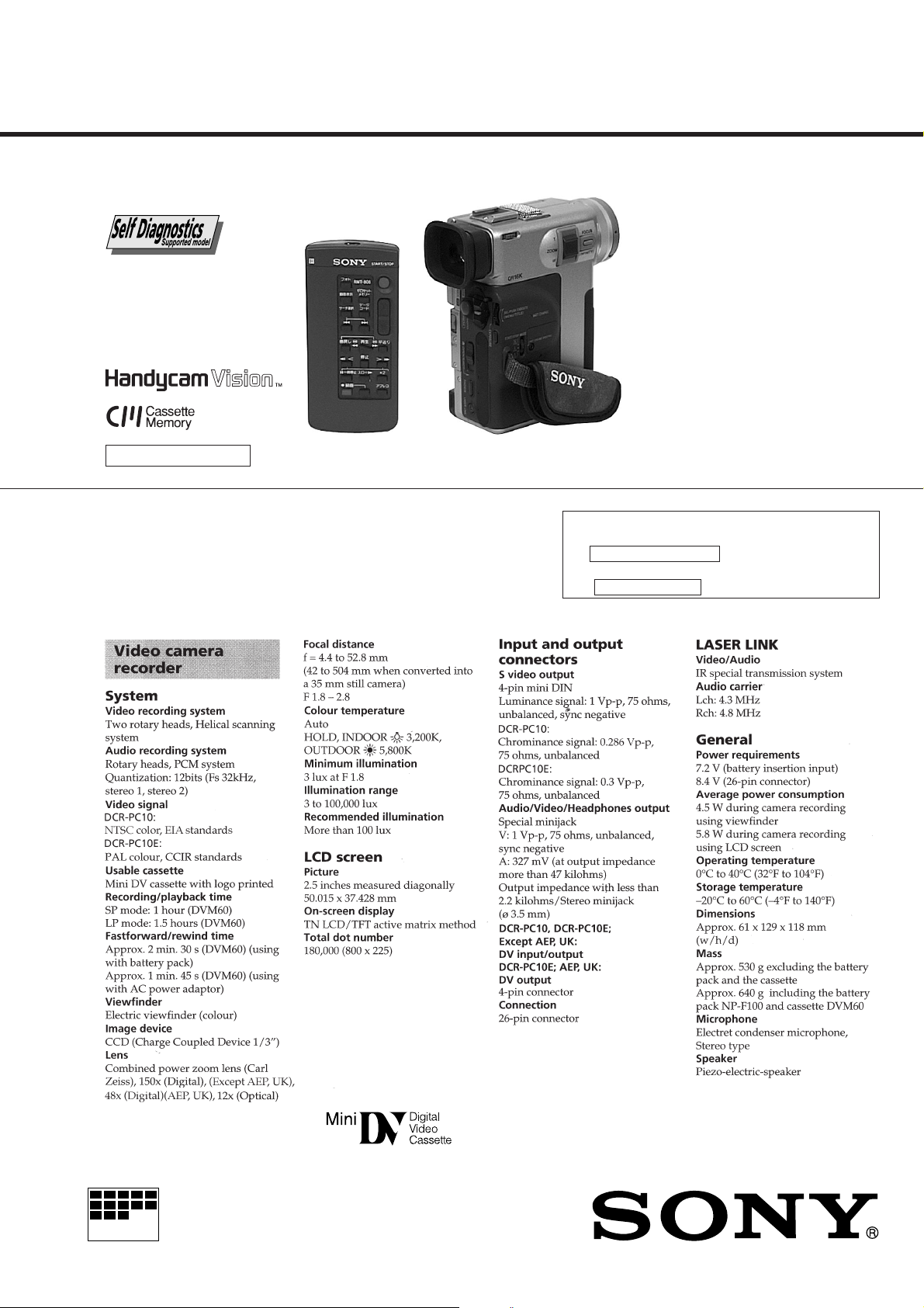
DCR-PC10/PC10E
RMT-808/809
SERVICE MANUAL
D200 MECHANISM
NTSC model: DCR-PC10
PAL model: DCR-PC10E
Photo : DCR-PC10E
: RMT-808
SPECIFICATIONS
US Model
Canadian Model
DCR-PC10
AEP Model
UK Model
Australian Model
Chinese Model
DCR-PC10E
E Model
Hong Kong Model
Tourist Model
DCR-PC10/PC10E
For MECHANISM ADJUSTMENTS, refer to the
“DV MECHANICAL ADJUSTMENT MANUAL
33
3 D200 MECHANISM ” (9-973-981-11),
33
“DV MECHANICAL ADJUSTMENT MANUAL
11
1 D MECHANISM ” (9-973-815-11).
11
MICROFILM
— Continued on next page —
DIGITAL VIDEO CAMERA RECORDER
Page 2
SAFETY-RELATED COMPONENT WARNING!!
COMPONENTS IDENTIFIED BY MARK ! OR DOTTED LINE WITH
MARK ! ON THE SCHEMATIC DIAGRAMS AND IN THE PARTS
LIST ARE CRITICAL TO SAFE OPERATION. REPLACE THESE
COMPONENTS WITH SONY PARTS WHOSE PART NUMBERS
APPEAR AS SHOWN IN THIS MANUAL OR IN SUPPLEMENTS
PUBLISHED BY SONY.
SAFETY CHECK-OUT
After correcting the original service problem, perform the following
safety checks before releasing the set to the customer.
ATTENTION AU COMPOSANT AYANT RAPPORT
À LA SÉCURITÉ!
LES COMPOSANTS IDENTIFÉS P AR UNE MARQ UE ! SUR LES
DIAGRAMMES SCHÉMA TIQUES ET LA LISTE DES PIÈCES SONT
CRITIQUES POUR LA SÉCURITÉ DE FONCTIONNEMENT. NE
REMPLACER CES COMPOSANTS QUE PAR DES PIÈSES SONY
DONT LES NUMÉROS SONT DONNÉS DANS CE MANUEL OU
DANS LES SUPPÉMENTS PUBLIÉS PAR SONY.
1. Check the area of your repair for unsoldered or poorly-soldered
connections. Check the entire board surface for solder splashes
and bridges.
2. Check the interboard wiring to ensure that no wires are
"pinched" or contact high-wattage resistors.
3. Look for unauthorized replacement parts, particularly
transistors, that were installed during a previous repair. Point
them out to the customer and recommend their replacement.
4. Look for parts which, through functioning, show obvious signs
of deterioration. Point them out to the customer and
recommend their replacement.
5. Check the B+ voltage to see it is at the values specified.
6. Flexible Circuit Board Repairing
• Keep the temperature of the soldering iron around 270˚C
during repairing.
• Do not touch the soldering iron on the same conductor of the
circuit board (within 3 times).
• Be careful not to apply force on the conductor when soldering
or unsoldering.
— 2 —
Page 3

TABLE OF CONTENTS
SERVICE NOTE
1. CABINET (L) ASSEMBLY REMOVAL WHEN THE
CASSETTE HOLDER STOPS HALFWAY DURING
LOADING OR UNLOADING ·········································· 6
2. HANDLING THE VC, MR BOARDS ······························ 6
3. SPECIAL PRECAUTIONS ON DISCONNECTION OF
CONNECTOR A TTACHED TO
THE FLEXIBLE BOARD ················································· 6
SELF-DIAGNOSIS FUNCTION
1. Self-diagnosis Function ······················································ 7
2. Self-diagnosis display························································· 7
3. Service Mode Display ························································ 7
3-1. Display Method ·································································· 7
3-2. Switching of Backup No. ··················································· 7
3-3. End of Display···································································· 7
4. Self-diagnosis Code Table ·················································· 8
1. GENERAL
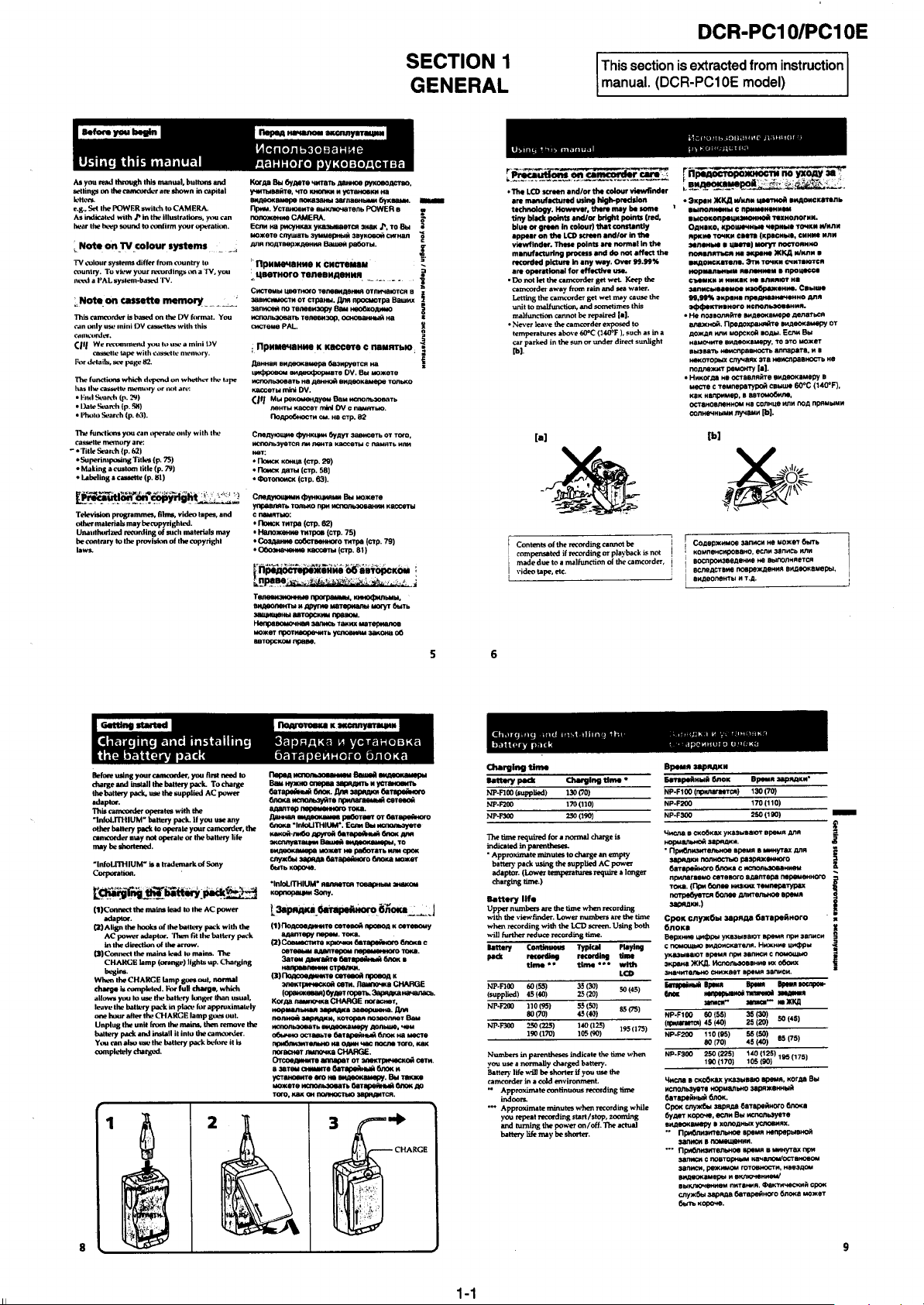
Before you begin
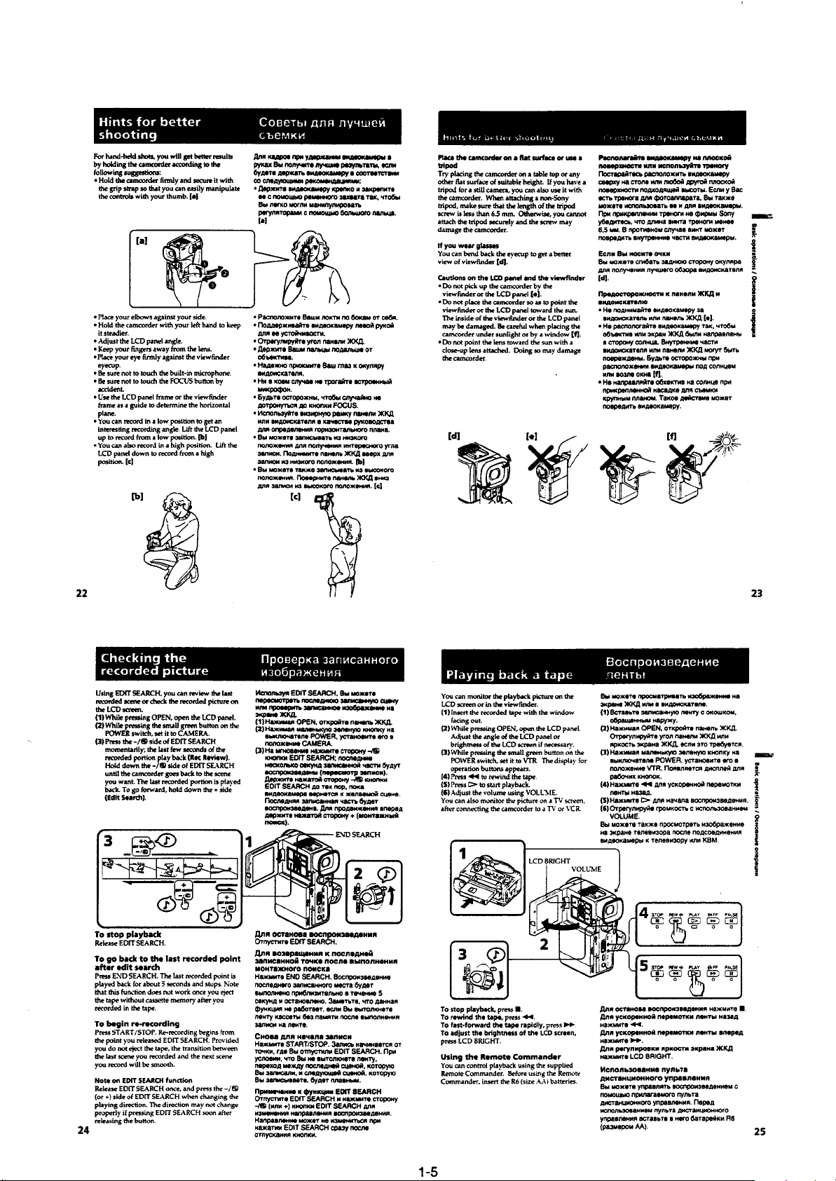
Using this manual ··································································1-1
Getting started
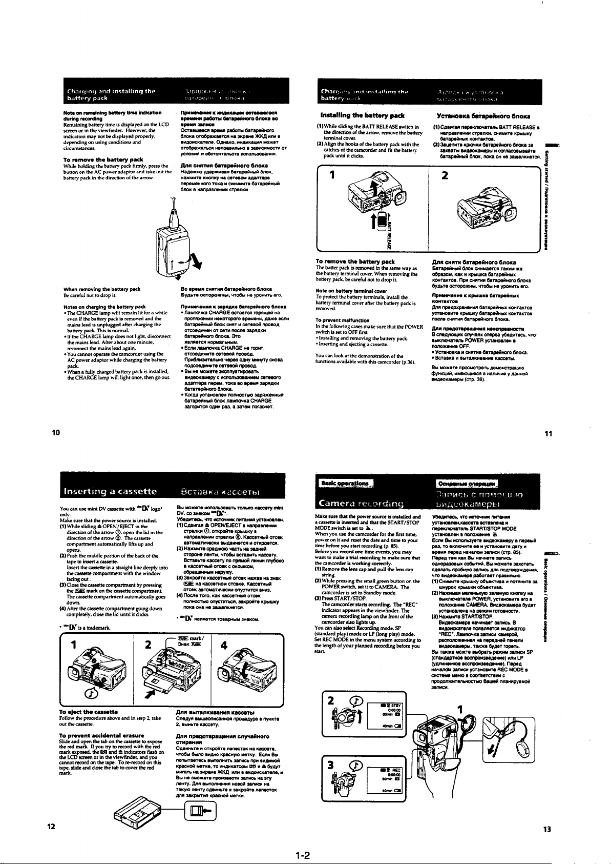
Charging and installing the battery pack ·······························1-1
Inserting a cassette ·································································1-2
Basic operations
Camera recording···································································1-2
Hints for better shooting ························································1-5
Checking the recorded picture ···············································1-5
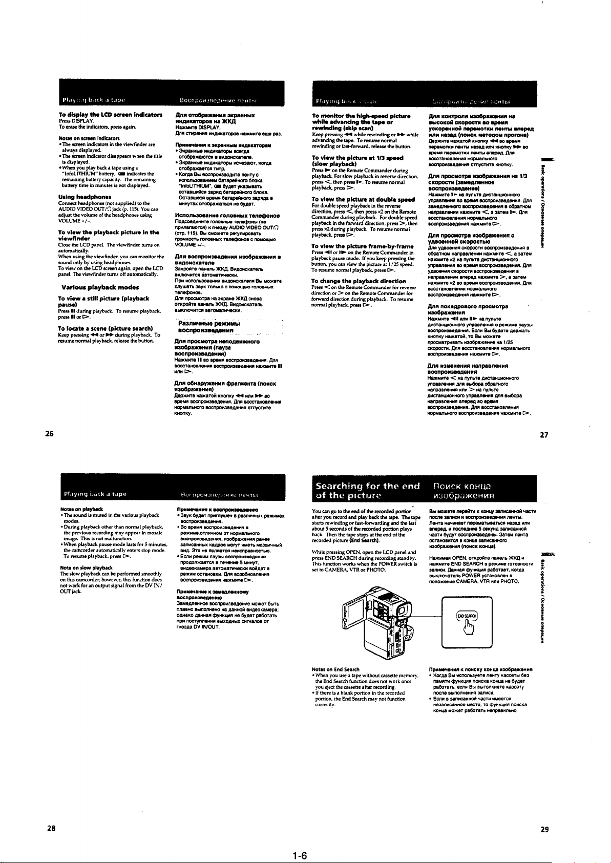
Playing back a tape ································································1-5
Searching for the end of the picture·······································1-6
Advanced operations
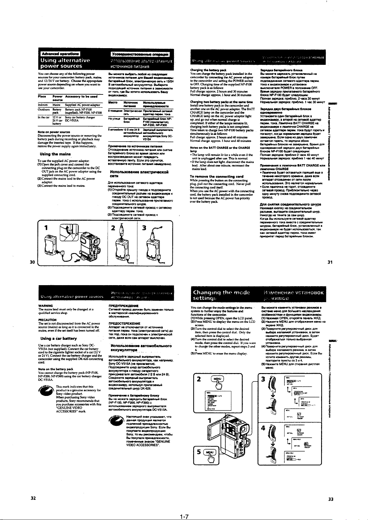
Using alternative power sources ············································1-7
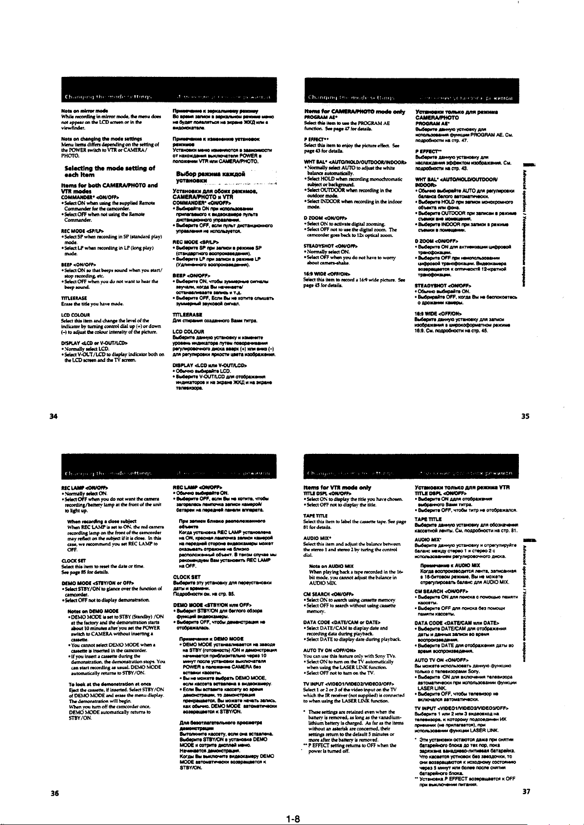
Changing the mode settings···················································1-7
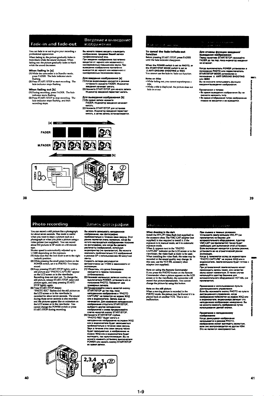
Fade-in and fade-out ······························································1-9
Photo recording······································································1-9
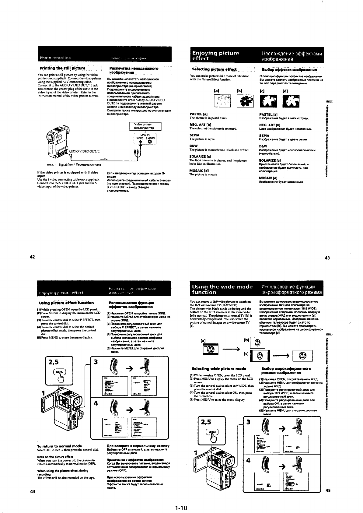
Enjoying picture effect ························································1-10
Using the wide mode function ·············································1-10
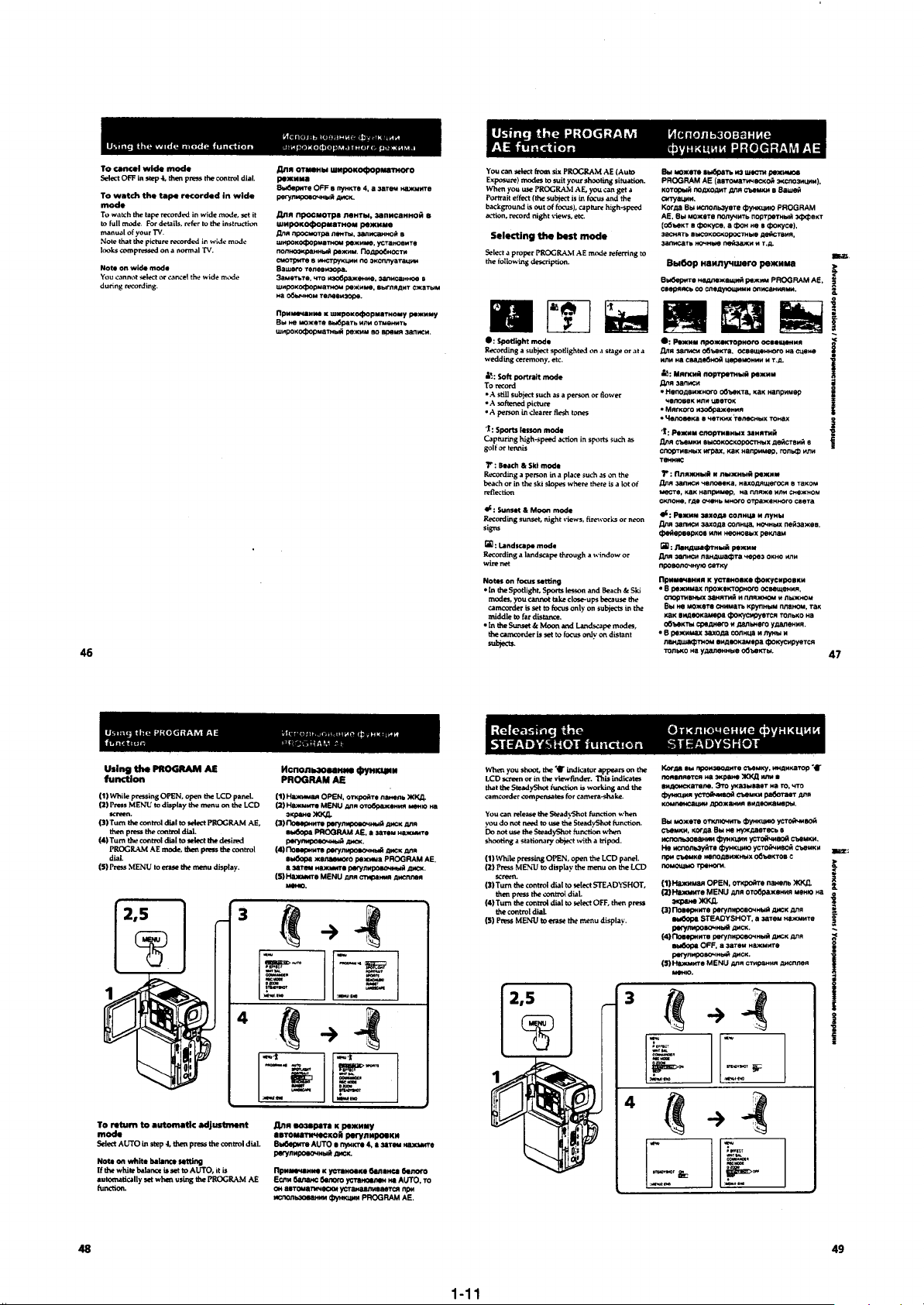
Using the PROGRAM AE function·····································1-11
Releasing the STEADYSHOT function ······························ 1-11
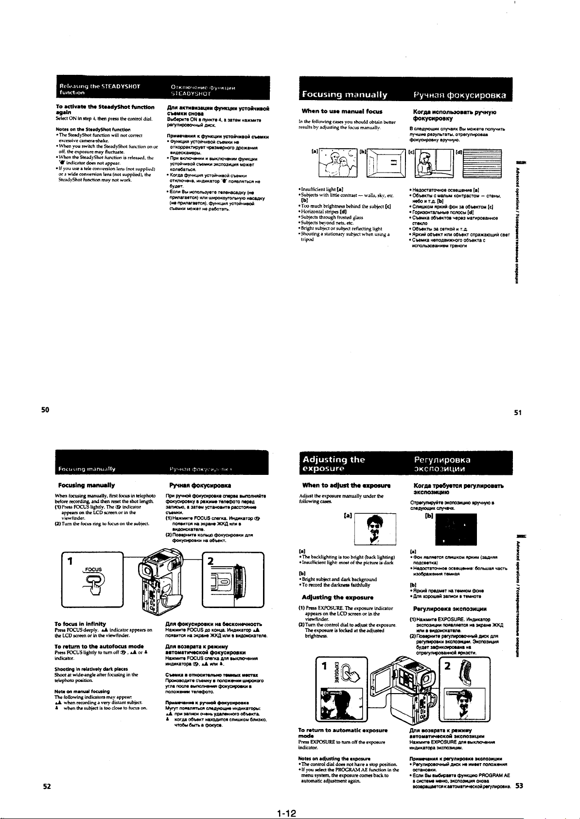
Focusing manually·······························································1-12
Adjusting the exposure ························································1-12
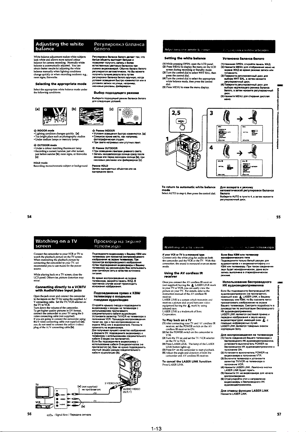
Adjusting the white balance·················································1-13
Watching on a TV screen ·····················································1-13
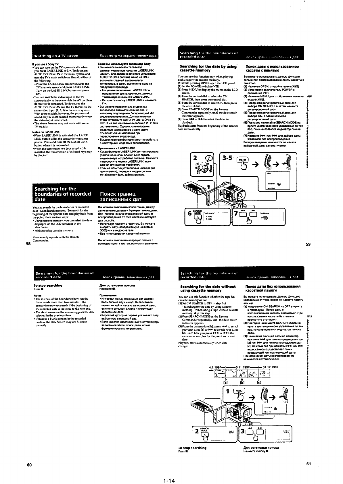
Searching for the boundaries of recorded data ····················1-14
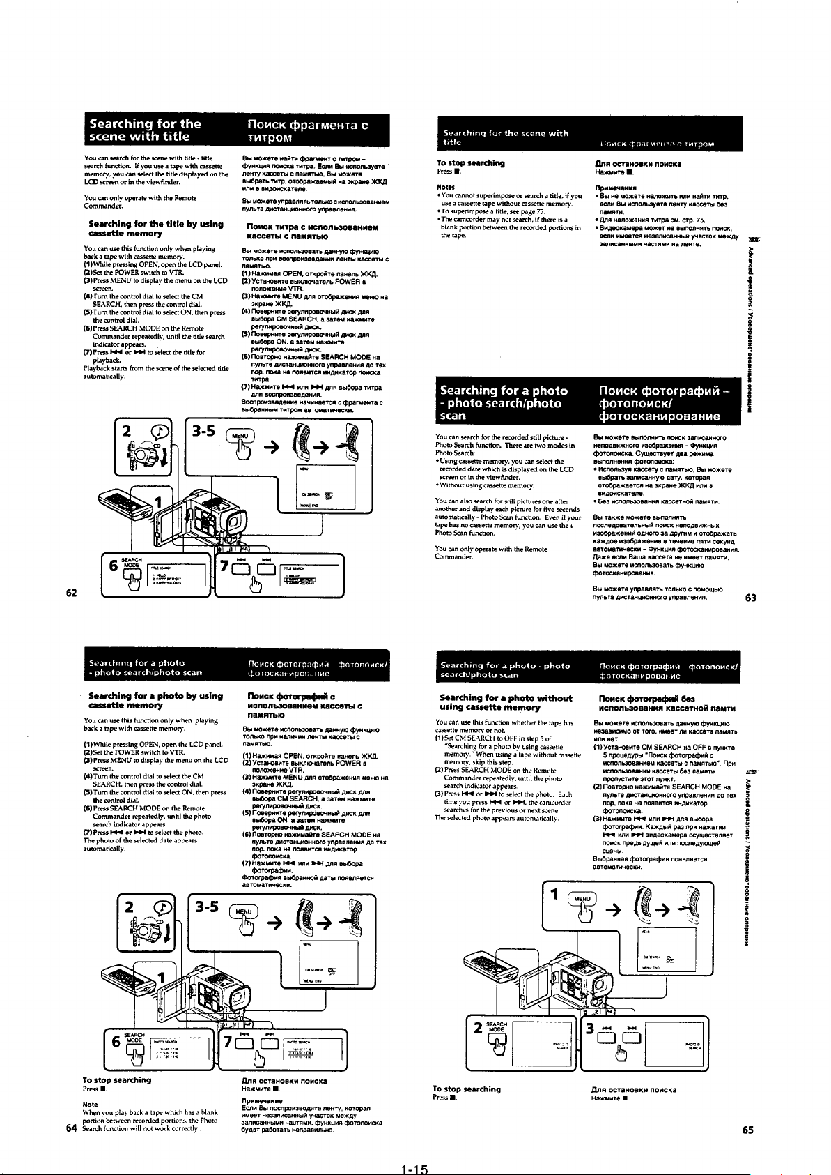
Searching for the scene with title·········································1-15
Searching for a photo-photo search/photo scan···················1-15
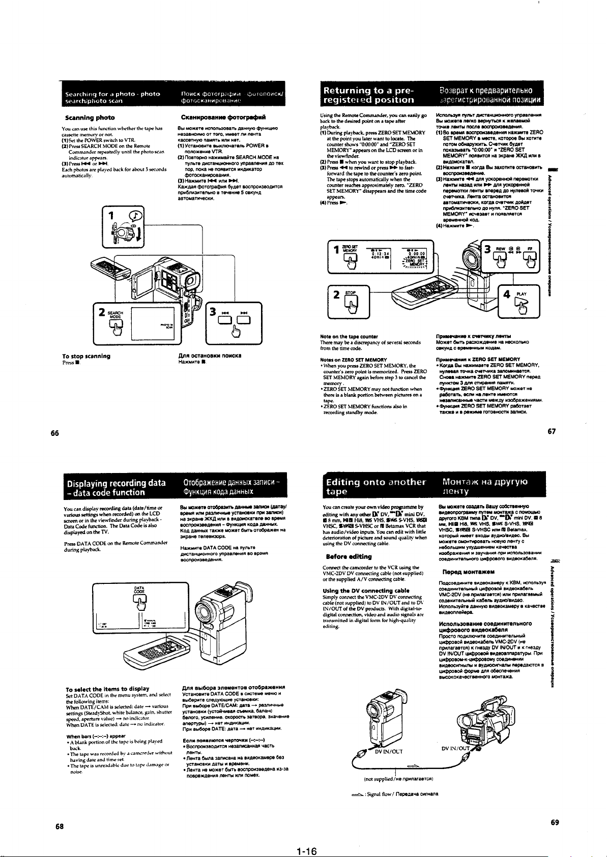
Returning to a preregistered position···································1-16
Displaying recording data-data code function ·····················1-16
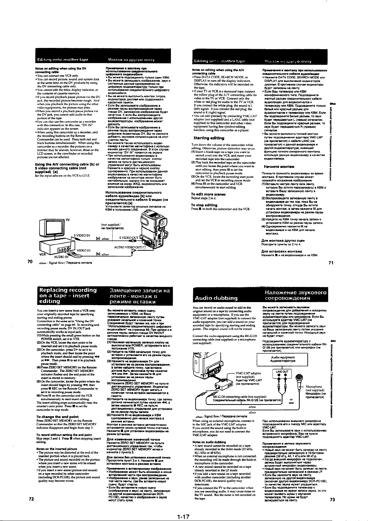
Editing onto another tape·····················································1-16
Replacing recording on a tape-insert editing ·······················1-17
Audio dubbing ·····································································1-17
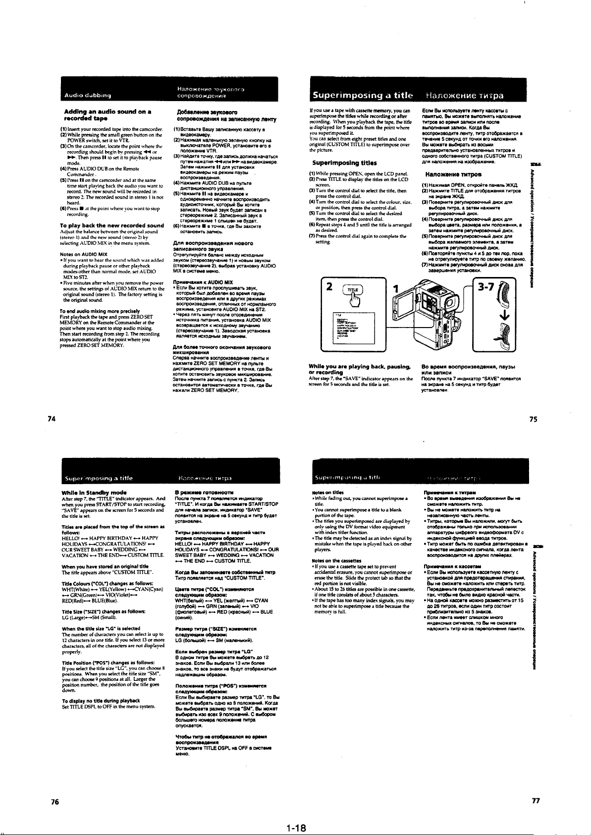
Superimposing a title ···························································1-18
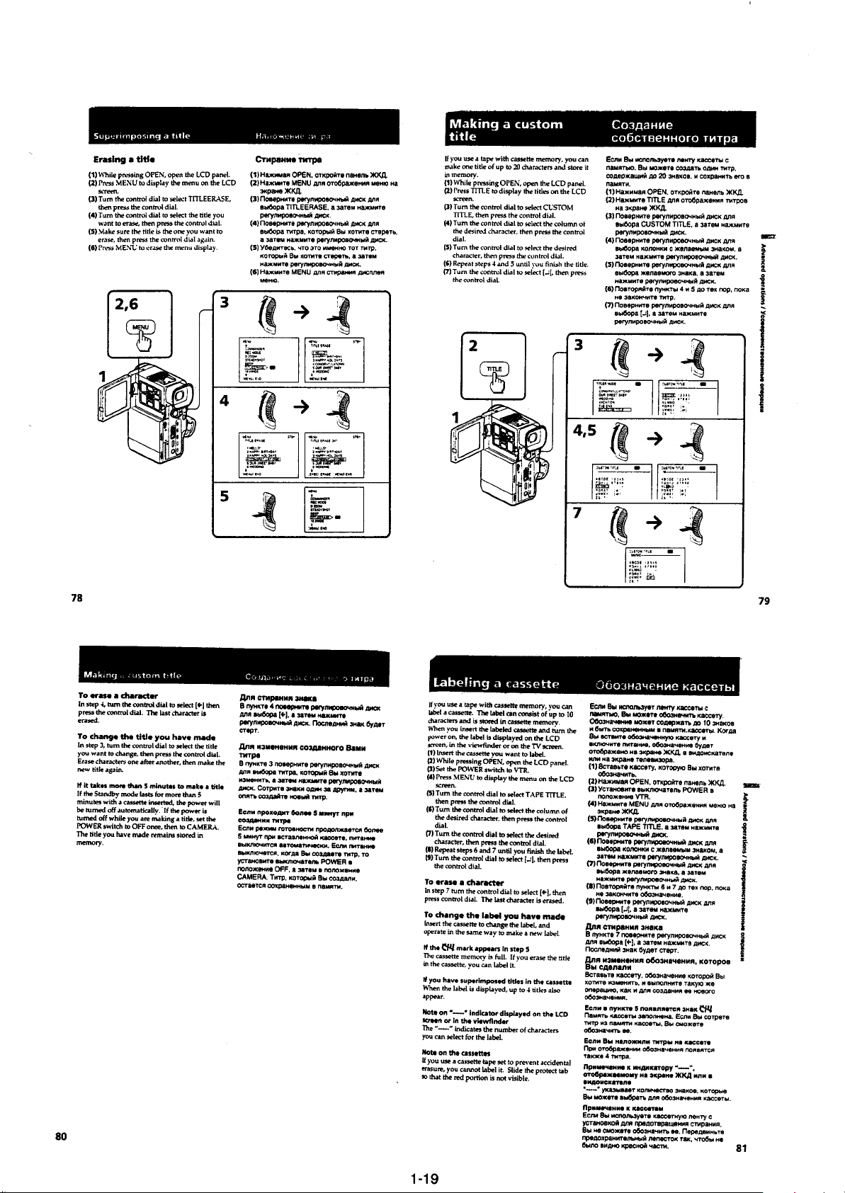
Making a custom title ··························································1-19
Labeling a cassette ·······························································1-19
Additional information
Usable cassettes and playback modes··································1-20
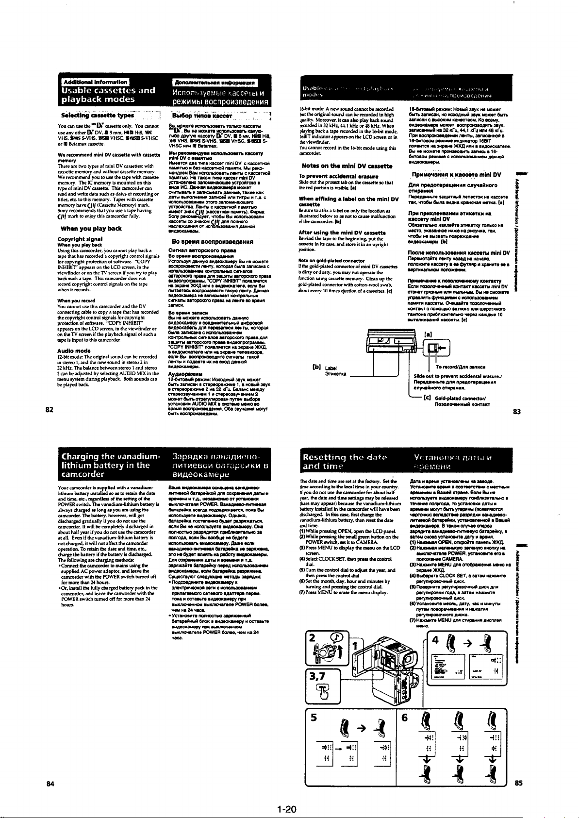
Charging the vanadium-lithium battery in the camcorder ···1-20
Resetting the data and time··················································1-20
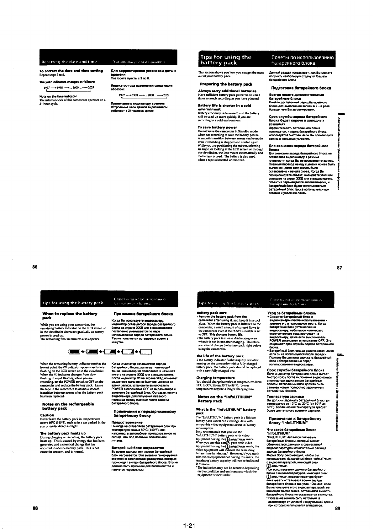
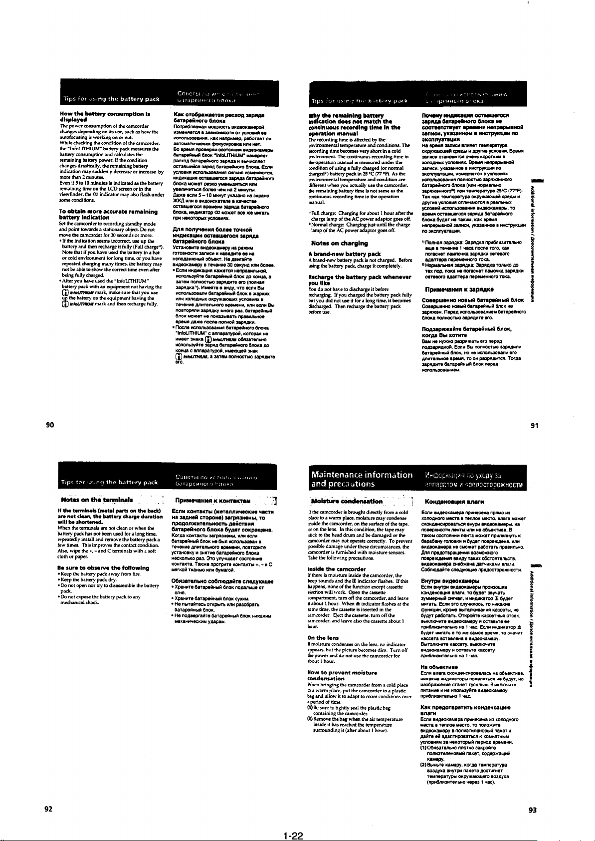
Tips for using the battery pack ············································1-21
Maintenance information and precautions···························1-22
Using your camcorder abroad··············································1-24
Trouble check ······································································1-24
Self-diagnosis function ························································1-25
Identifying the parts ·····························································1-25
Warning indicators ·······························································1-28
2 DISASSEMBLY
2-1. CASSETTE (L) ASSEMBLY ·········································2-1
2-2. CONTROL SWITCH BLOCK (FK-4850) (1)················2-2
2-3. CONTROL SWITCH BLOCK (FK-4850) (2)················2-2
2-4. NOTES ON REPLACING CONTROL
SWITCH BLOCK (FK-4850) ·········································2-3
2-5. MECHANISM DECK BLOCK ······································2-4
2-6. LENS DEVICE (LSV-590A),
EVF BLOCK ASSEMBLY ·············································2-4
2-7. VC-199 BOARD ·····························································2-4
2-8. DD-103 BOARD ·····························································2-5
2-9. PD-97 BOARD, ND5500, LCD901································2-5
2-10. SERVICE POSITION-1
(MAINLY FOR VIDEO/AUDIO SYSTEM CHECKS OR
ADJUSTMENTS) ···························································2-6
2-11. SERVICE POSITION-2
(MAINLY FOR CAMERA SYSTEM CHECKS OR
ADJUSTMENTS) ···························································2-7
2-12. CIRCUIT BOARDS LOCATION···································2-8
3. BLOCK DIAGRAMS
3-1. OVERALL BLOCK DIAGRAM ····································3-1
3-2. POWER SUPPLY BLOCK DIAGRAM ·························3-6
4. PRINTED WIRING BOARDS AND
SCHEMATIC DIAGRAMS
4-1. FRAME SCHEMATIC DIAGRAM ······························· 4-1
4-2. PRINTED WIRING BOARDS AND
SCHEMATIC DIAGRAMS ············································4-4
• CD-175 (CCD IMAGER)
PRINTED WIRING BOARD ·························4-5
• CD-175 (CCD IMAGER)
SCHEMATIC DIAGRAM ······························4-7
• VC-199 (MAIN) PRINTED WIRING BOARD ·······4-12
• VC-199 (CAMERA) SCHEMATIC DIAGRAM ······4-17
• VC-199 (LENS DRIVE)
SCHEMATIC DIAGRAM ····························4-21
• VC-199 (I/O) SCHEMATIC DIAGRAM·················· 4-23
• VC-199 (BLOCKING) SCHEMATIC DIAGRAM ··4-26
• VC-199 (ECC, TBC, CHCD)
SCHEMATIC DIAGRAM ····························4-29
• VC-199 (AUDIO SIGNAL PROCESS)
SCHEMATIC DIAGRAM ····························4-32
• VC-199 (DV I/O) SCHEMATIC DIAGRAM ···········4-35
• VC-199 (IR TRANSMITTER)
SCHEMATIC DIAGRAM ····························4-38
• VC-199 (RGB DECODER)
SCHEMATIC DIAGRAM ····························4-41
• VC-199 (MODE CONTROL),
FK-4850, ME-4850 (FUNCTION SWITCH BLOCK)
SCHEMATIC DIAGRAM ····························4-45
• VC-199 (AUDIO CONTROL)
SCHEMATIC DIAGRAM ····························4-49
• VC-199 (AUDIO) SCHEMATIC DIAGRAM ·········· 4-53
• MR-39 (REC/PB AMP, SERVO)
PRINTED WIRING BOARD -11·················4-57
• MR-39 (REC/PB AMP, SERVO)
PRINTED WIRING BOARD -12·················4-60
• CC-100 (TRANSLATION),
MR-39 (REC/PB AMP (1))
SCHEMATIC DIAGRAMS··························4-63
• CC-100 (TRANSLATION)
PRINTED WIRING BOARD ·······················4-66
• MR-39 (REC/PB AMP (2))
SCHEMATIC DIAGRAM ····························4-67
— 3 —
Page 4

• MR-39 (SERVO),
FP-242/FP-584 (TAPE SENSOR)
SCHEMATIC DIAGRAM ····························4-71
• FP-242/FP-584 (TAPE SENSORS)
PRINTED WIRING BOARDS·····················4-75
• PD-97 (LCD DRIVER)
PRINTED WIRING BOARD ·······················4-77
• PD-97 (LCD RGB DRIVER)
SCHEMATIC DIAGRAM ····························4-81
• PD-97 (TIMING GENERATOR)
SCHEMATIC DIAGRAM ····························4-84
• PD-97 (LCD, POWER SUPPLY FOR LCD BACK
LIGHT) SCHEMATIC DIAGRAM ·························· 4-87
• VF-117 (EVF) PRINTED WIRING BOARD ···········4-90
• VF-117 (EVF, POWER SUPPLY FOR EVF BACK
LIGHT) SCHEMATIC DIAGRAM ·························· 4-93
• VF-117 (EVF RGB DRIVER)
SCHEMATIC DIAGRAM ····························4-96
• DD-103 (POWER SUPPLY)
SCHEMATIC DIAGRAM ····························4-99
• DD-103 (I/O) SCHEMATIC DIAGRAM ··············· 4-102
• DD-103 (POWER SUPPLY, I/O)
PRINTED WIRING DIAGRAM ················4-105
5. ADJUSTMENTS
5-1. CAMERA SECTION ADJUSTMENT ···························5-1
1-1. PREPARATIONS BEFORE ADJUSTMENT·················5-1
1-1-1.List of Service Tools ························································5-1
1-1-2.Preparations ·····································································5-3
1-1-3. Power Supply Procedure·················································5-3
1-1-4.Precautions ······································································5-4
1. Setting the Switches ························································5-4
2. Adjustment Sequence ······················································5-4
3. Subject ·············································································5-4
1-2. CAMERA SYSTEM ADJUSTMENTS ··························5-5
1-2-1.Adjustment Points When Major Parts
Have Been Replaced ······················································· 5-5
1-2-2.Initialization of Page F data·············································5-5
1-2-3.Modification of Page F data ············································5-6
1-2-4.PLL Adjustment (VC-199 Board)[Procedure-1]·············5-6
1-2-5.PLL Adjustment (VC-199 Board)[Procedure-2]·············5-7
1-2-6.Original Oscillation Adjustment (VC-199 Board) ·········· 5-7
1-2-7.HALL Adjustment ···························································5-8
1-2-8.Flange Back Adjustment (1)··········································5-10
1-2-9.Flange Back Adjustment (2)·········································· 5-11
1-2-10. Flange Back Check ·····················································5-12
1-2-11. Picture Frame Setting··················································5-13
1-2-12. Color Reproduction Adjustment·································5-14
1-2-13. Color Reproduction Check ·········································5-15
1-2-14. IRIS IN/OUT Adjustment ···········································5-16
1-2-15. MAX GAIN Adjustment·············································5-17
1-2-16. Auto White Balance Reference Data Input ·················5-18
1-2-17. Auto White Balance Adjustment································· 5-19
1-2-18. White Balance Check··················································5-20
1-2-19. Velocity Sensor Sensitivity Adjustment ······················5-21
1-3. COLOR ELECTRONIC VIEWFINDER SYSTEM
ADJUSTMENTS···························································5-22
1-3-1.EVR Initial Data Input ··················································5-22
1-3-2.VCO Adjustment (VF-117 Board) ································5-23
1-3-3.BRIGHT Adjustment (VF-117 Board) ··························5-23
1-3-4.CONTRAST Adjustment (VF-117 Board) ····················5-24
1-3-5.Backlight Current Consumption Adjustment
(VF-117 Board) ·····························································5-25
1-3-6.White Balance Adjustment············································5-26
1-4. LCD SYSTEM ADJUSTMENTS·································5-27
1-4-1.LCD Initial Data Input ··················································5-27
1-4-2.15.5 V Adjustment (PD-97 Board)································5-28
1-4-3.VCO Adjustment (PD-97 Board) ··································5-28
1-4-4.BRIGHT Adjustment (PD-97 Board)····························5-29
1-4-5.CONTRAST Adjustment (PD-97 Board)······················5-29
1-4-6.White Balance Adjustment············································5-30
1-5. ARRANGEMENT DIAGRAM FOR
ADJUSTMENT PARTS················································5-32
5-2. MECHANISM SECTION ADJUSTMENTS ···············5-37
2-1. OPERATING WITHOUT CASSETTE ························5-37
2-2. TAPE PATH ADJUSTMENT········································5-37
1. Preparations for Adjustment··········································5-37
2. Procedure after operation ··············································5-37
5-3. VIDEO SECTION ADJUSTMENTS ···························5-38
3-1. PREPARATIONS BEFORE ADJUSTMENT···············5-38
3-1-1.Equipments to be Used ··················································5-38
3-1-2.Power Supply Procedure ···············································5-38
3-1-3.Precautions in Adjustment·············································5-39
3-1-4.Adjusting Connectors ····················································5-39
3-1-5.Connection of Equipment··············································5-40
3-1-6.Output Level and Impedance ········································5-40
3-2. POWER SUPPLY SYSTEM ADJUSTMENTS············5-41
1. Power Supply Voltage Check (DD-103 Board)·············5-41
3-3. SYSTEM CONTROLLER SYSTEM
ADJUSTMENTS···························································5-42
3-3-1. Initializing the Page D Data··········································5-42
3-3-2.Modification of Page D Data·········································5-42
3-3-3.Initializing the Page C Data···········································5-43
3-3-4.Modification of Page C Data ·········································5-43
3-3-5.Battery Down Adjustment ·············································5-44
3-4. SERVO SYSTEM ADJUSTMENTS ····························5-45
1. T Reel FG Duty Adjustment and CSerr Adjustment
(MR-39 Board) ······························································5-45
2. Switching Position Adjustment (MR-39 Board) ···········5-46
3-5. VIDEO SYSTEM ADJUSTMENTS·····························5-47
3-5-1.RF Block Adjustment (MR-39 Board) ··························5-47
1. Record Current Adjustment/
Frequency Response Check···········································5-47
2. PLL fo Adjustment (MR-39 Board) ······························5-48
3. CLK DELAY Adjustment (MR-39 Board) ···················5-49
4. AGC Center Level Adjustment (VC-199 Board)··········5-50
5. PLL Capture Range Adjustment (VC-199 Board) ········5-51
6. AEQ Adjustment (VC-199 Board)································5-52
3-5-2.Base Band Block Adjustment········································5-53
1. Composite Output Y Level Adjustment
(VC-199 Board)·····························································5-53
2. Composite Output Chroma Level Adjustment
(VC-199 Board)·····························································5-53
3. S-Y Output Level Adjustment (VC-199 Board)············5-54
4. S-C Output Chroma Level Adjustment
(VC-199 Board)·····························································5-54
3-5-3.Clock Adjustment ··························································5-55
1. IC1900 27MHz XTAL fo adjustment
(VC-199 Board)·····························································5-55
3-5-4.BIST Check ···································································5-56
4-1. Playback System Check ················································5-56
1. IC1701 (D1) playback system check·····························5-56
2. IC1901(A1) playback system check······························5-57
3. IC1500 (U1) playback system check·····························5-57
4-2. Recording System Check ··············································5-58
3-6. IR TRANSMITTER ADJUSTMENTS·························5-60
3-6-1.Preparations ···································································5-60
1. Equipment Connection ··················································5-60
3-6-2.IR Video Carrier Frequency Adjustment ·······················5-60
3-6-3.IR Video Deviation Adjustment ····································5-61
3-6-4.IR Audio Deviation Adjustment ····································5-61
3-7. AUDIO SYSTEM ADJUSTMENTS ····························5-62
3-7-1.Preparations ···································································5-62
3-7-2.Playback Level Check ···················································5-63
— 4 —
Page 5

3-7-3.EXT MIC Input Gain and L/R Balance Check ·············5-63
3-7-4.EXT MIC Input Separation Check ································5-63
3-7-5.EXT MIC Input Distortion Factor Check······················5-63
3-7-6.EXT MIC Input Noise Level Check······························5-64
3-8. ARRANGEMENT DIAGRAM FOR
ADJUSTMENT PARTS ················································5-65
5-4. SERVICE MODE··························································5-71
4-1. ADJUSTMENT REMOTE COMMANDER
(RM-95 UPGRADED) ··················································5-71
1. Using the Adjustment Remote Commander·················· 5-71
2. Precautions When Using the Adjustment
Remote Commander······················································5-72
4-2. SERVICE MODE··························································5-74
4-2-1.Setting the Test Mode····················································5-74
4-2-2.Use History Check·························································5-74
4-2-3.Emergency Memory Address ········································5-75
4-2-4.EMG Code (Emergency Code) ····································· 5-76
4-2-5.MSW Code ····································································5-76
4-2-6.Key Input Check (A/D Port) ·········································5-77
4-2-7.Page F Address List·······················································5-78
4-2-8.Page D Address List ······················································5-81
4-2-9.Page C Address List ······················································5-83
6. REPAIR PARTS LIST
6-1. EXPLODED VIEWS ······················································6-1
6-1-1.CABINET (L) ASSEMBLY SECTION ··························6-1
6-1-2.MAIN BOARDS SECTION ···········································6-2
6-1-3.CABINET (R) ASSEMBLY, LCD PANEL SECTION···6-3
6-1-4.EVF, ZOOM LENS SECTION ·······································6-4
6-1-5.CASSETTE COMPARTMENT BLOCK SECTION······6-5
6-1-6.LS CHASSIS BLOCK SECTION ··································6-6
6-1-7.MECHANISM CHASSIS BLOCK SECTION-1 ···········6-7
6-1-8.MECHANISM CHASSIS BLOCK SECTION-2 ···········6-8
6-2. ELECTRICAL PARTS LIST ··········································6-9
* There is the color reproduction standard frame at the back of
the book.
— 5 —
Page 6
SER VICE NOTE
1. CABINET (L) ASSEMBLY REMOVAL WHEN THE CASSETTE HOLDER STOPS
HALFWAY DURING LOADING OR UNLOADING
(Do not remove cabinet (L) assembly in the state that the cassette holder stops halfway.)
Note 1: Unloading operation in the state that the tape is in the set causes tape damage. So do not perform the unloading operation.
Note 2: Do not perform the following operation in the state that the unregulated power supply is connected.
(Disconnect battery or AC adapter)
1) Remove screws securing cabinet (L) assembly referring the “SECTION 2. DISASSEMBLY”.
2) Put cabinet (L) assembly up and apply power supply to loading motor with tester leads or the like from gaps.
+
–
Regulated Power Supply
4.0V
±
0.2V
Cabinet (L) Assembly
2. HANDLING THE VC, MR BOARDS
Never heat the VC and MR boards with hot air . (Malfunctions may
result.)
Also remove after dehumidifying.
: Loading
Loading Motor
3. SPECIAL PRECAUTIONS ON
DISCONNECTION OF CONNECTOR
A TT ACHED TO THE FLEXIBLE
BOARD
Connector
*
*
• Apply force in the arrow (÷) direction and disconnect.
• Do not apply force in the * direction as this will cause the solder
(of the pin) to float easily.
• When touching the pins with the solder iron, do not touch other
parts. (Deformation may occur.)
• Ensure no folding lines are formed on the flexible board. (This
will cause the internal copper film to cut easily.)
— 6 —
Flexible board
Page 7
SELF-DIAGNOSIS FUNCTION
r
1. Self-diagnosis Function
When problems occur while the unit is operating, the self-diagnosis
function starts working, and displays on the LCD window what to
do. This function consists of two display; self-diagnosis display and
service mode display.
Details of the self-diagnosis functions are provided in the Instruction
manual.
Blinks at 3.2Hz
3 1C
Repaired by:
C : Corrected by customer
H : Corrected by dealer
E : Corrected by service
engineer
Block
Indicates the appropriate
step to be taken.
E.g.
31 ....Reload the tape.
32 ....Turn on power again.
2. Self-diagnosis display
When problems occur while the unit is operating, the counter of the
LCD window shows a 4-digit display consisting of an alphabet and
numbers, which blinks at 3.2 Hz. This 5-character display indicates
the “repaired by:”, “block” in which the problem occurred, and
“detailed code” of the problem.
LCD screen/viewfinde
1 1
Detailed Code
Refer to page 8
Self-diagnosis Code Table.
3. Service Mode Display
The service mode display shows up to six self-diagnosis codes shown in the past.
3-1. Display Method
While pressing the “STOP” key , set the power switch from OFF to “VTR or PLAYER”, and continue pressing the “STOP” key for 5 seconds
continuously. The service mode will be displayed, and the counter will show the backup No. and the 5-character self-diagnosis codes.
LCD screen/viewfinder
C : 3 1 : 1 1[3]
Backup No.
Order of previous errors
3-2. Switching of Backup No.
By rotating the control dial, past self-diagnosis codes will be shown in order. The backup No. in the [] indicates the order in which the
problem occurred. (If the number of problems which occurred is less than 6, only the number of problems which occurred will be shown.)
[1] : Occurred first time [4] : Occurred fourth time
[2] : Occurred second time [5] : Occurred fifth time
[3] : Occurred third time [6] : Occurred the last time
self-diagnosis codes
Control dial
3-3. End of Display
Turning OFF the power supply will end the service mode display.
Note: The self-diagnosis display data will be backed up by the coin-type lithium battery. When this coin-type lithium battery
(FK-4850 flexible board) is disconnected, the self-diagnosis data will be lost by initialization.
— 7 —
Page 8

4. Self-diagnosis Code Table
Self-diagnosis Code
Function
Repaired by:
C
C
C
C
C
C
C
C
C
C
C
C
C
C
C
C
C
C
C
C
C
C
C
E
E
E
E
Block
21
22
23
31
31
31
31
31
31
31
31
31
31
32
32
32
32
32
32
32
32
32
32
61
61
62
62
Detailed
Code
00
00
00
10
11
20
21
22
23
24
30
40
42
10
11
20
21
22
23
24
30
40
42
00
10
00
01
Symptom/State
Condensation.
Video head is dirty.
Non-standard battery is used.
LOAD direction. Loading does not
complete within specified time
UNLOAD direction. Loading does not
complete within specified time
T reel side tape slacking when unloading
S reel side tape slacking when unloading.
T reel fault
S reel fault
T reel fault
FG fault when starting capstan
FG fault when starting drum
FG fault during normal drum operations
LOAD direction loading motor time-
out
UNLOAD direction loading motor
time-out
T reel side tape slacking when
unloading.
S reel side tape slacking when
unloading.
T reel fault
S reel fault
T reel fault
FG fault during normal capstan
operations
FG fault when starting drum
FG fault during normal drum
operations
Difficult to adjust focus
(Cannot initialize focus.)
Zoom operations fault
(Cannot initialize zoom lens.)
Steadyshot function does not work
well. (With pitch angular velocity
sensor output stopped.)
Steadyshot function does not work
well. (With yaw angular velocity sensor
output stopped.)
.
Correction
Remove the cassette, and insert it again after one hour.
Clean with the optional cleaning cassette.
Use the info LITHIUM battery.
Load the tape again, and perform operations from the beginning.
Load the tape again, and perform operations from the beginning.
Load the tape again, and perform operations from the beginning.
Load the tape again, and perform operations from the beginning.
Load the tape again, and perform operations from the beginning.
Load the tape again, and perform operations from the beginning.
Load the tape again, and perform operations from the beginning.
Load the tape again, and perform operations from the beginning.
Load the tape again, and perform operations from the beginning.
Load the tape again, and perform operations from the beginning.
Remove the battery or power cable, connect, and perform
operations from the beginning.
Remove the battery or power cable, connect, and perform
operations from the beginning.
Remove the battery or power cable, connect, and perform
operations from the beginning.
Remove the battery or power cable, connect, and perform
operations from the beginning.
Remove the battery or power cable, connect, and perform
operations from the beginning.
Remove the battery or power cable, connect, and perform
operations from the beginning.
Remove the battery or power cable, connect, and perform
operations from the beginning.
Remove the battery or power cable, connect, and perform
operations from the beginning.
Remove the battery or power cable, connect, and perform
operations from the beginning.
Remove the battery or power cable, connect, and perform
operations from the beginning.
Inspect the lens block focus reset sensor (Pin @¡ of CN100 of
CD-175 board) when focusing is performed when the focus
button of the remote control (e.g. RM-95) is pressed in the focus
fixing mode, and the focus motor drive circuit (IC204, IC404 of
VC-199 board) when the focusing is not performed.
Inspect the lens block zoom reset sensor (Pin !¡ of CN100 of
CD-175 board) when zooming is performed when the zoom lens
is operated and the zoom motor drive circuit (IC204, 404 of VC199 board) when zooming is not performed.
Inspect pitch angular velocity sensor (SE501 of FP-615 flexible
board) peripheral circuits.
Inspect yaw angular velocity sensor (SE500 of CD-175 board)
peripheral circuits.
— 8 —
Page 9
Page 10
Page 11
Page 12
Page 13
Page 14
Page 15
Page 16
Page 17
Page 18
Page 19
Page 20
Page 21
Page 22
Page 23
Page 24
Page 25
Page 26
Page 27
Page 28
Page 29
Page 30
Page 31

Page 32

Page 33

Page 34

Page 35

Page 36

Page 37

SECTION 2
DISASSEMBLY
NOTE : Follow the disassembly procedure in the numerical order given.
2-1. CASSETTE (L) ASSEMBLY
1
Two screws (K2 × 4)
2
Accessory shoe
3
Accessory plate (2)
!º
4
Screw (M1.7 × 2.5)
DCR-PC10/PC10E
!£
Cabinet (L) assembly
Open the cabinet (L)
assembly halfway.
!¡
retainer plate in the
arrow
a
Turn FK flexible
a
direction.
!™
FP-605 flexible board
5
Two screws (M1.7 × 2.5)
6
7
Screw (M1.7 × 2.5)
2-1
8
9
Screw
(M1.7
×
2.5)
Page 38

2-2. CONTROL SWITCH BLOCK (FK-4850) (1)
1
Three screws (M1.7 × 2.5)
6
2
Focus/zoom section of
control switch block
(FK-4850)
Cabinet (L)
Both sided adhesive tape (Peel off it
not to break the flexible cable.)
Screw (M1.7 × 2.5)
7
G lock frame
6
Screw
(M1.7
3
Screw
(M1.7
9
×
2.5)
4
Door open/close detect
switch section of control
switch block (FK-4850)
×
2.5)
8
Two screws
(M1.7
8
Screw
(M1.7
×
2.5)
5
Open the cassette lid by sliding
the cassette door open button in
the arrow
claws on two position.
×
2.5)
!º
a
direction to put off
a
To be continued to the item 2-3.
CONTROL SWITCH BLOCK
(FK-4850) (2).
2-3. CONTROL SWITCH BLOCK (FK-4850) (2)
!£
Two screws (TPM1.7 × 4)
!£
Screw
(see page 2-3)
!£
Screw (M2)
Grip arm assembly
Claw
a
!∞
Remove three claws and
pull off in the arrow
Claw
Claw
a
direction.
Claw
b
Claw
!§
Control switch block
Grip cabinet
assembly
Claw
!¢
Screw (M1.7 × 2.5)
!¢
Three screws
(M1.7
×
2.5)
!¶
Control switch block
Pull it off in the arrow
b
direction.
2-2
!™
Lithium battery case lid
!¡
Screw (BTP2 × 5)
Page 39

2-4. NOTES ON REPLACING CONTROL SWITCH BLOCK (FK-4850)
There are two types of the control switch block (FK-4850), parts
code suffix -11 and -12 (The supplied part for service is the suf fix 12 part only).
When replacing it -11 to -12, also it is necessary to replace the grip
arm assembly suffix -1 to -2 and screws suffix -11 to -31.
Discrimination between the suffix -11 and -12 of the
control switch block (FK-4850).
TYPE A : Combination with the control switch block parts
code suffix -11.
TYPE B : Combination with the control switch block parts
code suffix -12.
Power supply
Start/Stop
Grip cabinet assembly
TYPE A-1 TYPE A-2
Grip arm assembly
X-3947-792-2
Screw (M1.7
3-713-791-01
TYPE A
×
4)
Grip arm assembly
X-3947-792-1
Screw (M1.7
3-713-791-01
×
4)
Control switch
block
Grip arm assembly
Control switch block (FK-4850)
1-475-331-11
TYPE B
Grip arm assembly
X-3947-792-2
Control switch block (FK-4850)
1-475-331-12
Note: A screw used on TYPE B is longer than it used on TYPE A
to secure the grip arm assembly and the control switch
block (FK-4850) together. Be sure to use a long screw
(M1.7 × 6).
Screw (M1.7
3-713-791-31
×
6)
2-3
Page 40

2-5. MECHANISM DECK BLOCK
4
Mechanism deck block
1
Two step screws (M2)
1
Two step screws
2
DD-103 board
CN3900
@
3
CC-100 board
CN6250
(M2)
4
Remote control
window (I)
2-6. LENS DEVICE (LSV-590A), EVF
BLOCK ASSEMBLY
7
6
Screw
(M1.7
Lens device
(LSV-590A)
×
2.5)
3
VF-117 board
CN4400
1
Screw
(M1.7
5
plate
×
2.5)
2
EVF section
4
Screw
(M1.7
VC shield
×
2.5)
Note on mechanism deck attaching:
First attach the remote control window (I). or check the
remote control window (I) is already attached.
2-7. VC-199 BOARD
6
Connector
5
Connector
(From MIC1)
CN4700
9
Four screws
(M1.7
×
2.5)
(From PD-97 board)
VC-199 BOARD
!¡
CN2301
CN200
4
!º
DD-103 board
CN3700
(Note)
!™
Open the DV terminal cover
in the arrow
a
CN1000
VC-199 board
Battery plate assembly
3
Two screws
(M1.7
a
×
direction.
2.5)
CN1002
CN1001
CN4701
!£
VC-199 board
Note: Be sure to connect first CN3700 before attaching the
battery plate assembly.
b
7
(ME-4850)
8
From SP901
2-4
2
Shift the cabinet (bottom)
assembly in the arrow
direction.
1
Two screws (M1.7 × 2.5)
From control switch block
b
Page 41

2-8. DD-103 BOARD
1
Screw
(M1.7
3
Two screws
(M1.7
4
(M2
×
Three screws
×
6)
2
Battery terminal board
×
3)
3)
6
DD-103 board
Cabinet (bottom) assembly
2-9. PD-97 BOARD, ND5500, LCD901
8
Connector
!¡
Two screws (M1.7 × 2.5)
1
(From VC-199 board CN1001)
PD-97
BOARD
!™
PD-97 board
6
Plate (3), PD ground
!£
ND5500
Cold cathode fluorescent tube
7
Connector
(From VC-199 board CN1002)
9
LCD901 flexible board
!º
LCD901 LCD module
5
FP-484 flexible board
4
LCD case (L) assembly
3
Screw (M1.7 × 2.5)
2-5
2
Three screws
(M1.7
×
2.5)
Page 42

2-10.SERVICE POSITION-1
(MAINLY FOR VIDEO/AUDIO SYSTEM CHECKS OR ADJUSTMENTS)
1
Remove each board in the disassembly procedure.
2
Connect the specified jigs as shown in the figure.
(Some connectors can be connected reversely b y its shape .
So, note that its connection on removal.)
I/O board-1 jig
(J-6082-372-C)
DD-103: 26-pin MULTI connector
DD-103 board
Note: Do not apply excessive force to the flexible portion of DD-
103 board because of its shortness.
MR-39: CN3100↔Capstan motor flexible board
extension cable (18P)
(J-6082-374-A)
VIDEO AUDIO OUT/
HEADPHONES jack
Regulated dc power supply
(8.4V)
FK-4850
(Control switch block)
VC-199 board
MR-39 board
CPC terminal extension flexible board
(CPC-6 jig) (J-6082-370-A)
VC-199: CN6202
CPC-6 terminal board jig
(J-6082-371-A)
2-6
Page 43

2-11.SERVICE POSITION-2
l
(MAINLY FOR CAMERA SYSTEM CHECKS OR ADJUSTMENTS)
1
Remove each board in the disassembly procedure.
2
Connect the specified jigs as shown in the figure.
(Some connectors can be connected reversely b y its shape .
So, note that its connection on removal.)
CPC-6 terminal board jig
(J-6082-371-A)
CPC terminal extension flexible board
(CPC-6 jig) (J-6082-370-A)
VC-199: CN6202
MR-39 board
VC-199 board
Note: Do not apply excessive force to the flexible portion of DD-
103 board because of its shortness.
Mechanism deck block
Zoom lens
DD-103 board
FK-4850
(Control switch block)
Battery terminal
‘
Battery terminal
board
’
Regulated power supply
Box or pedesta
(8.4 V)
2-7
Page 44

2-12.CIRCUIT BOARDS LOCATION
CD-175 (CCD IMAGER)
PD-97 LCD RGB DRIVER,
TIMING GENERATOR,
LCD BACKLIGHT
MR-39
(REC/PB AMP, SERVO)
DD-103
(POWER SUPPLY, I/O)
VF-117 (EVF)
VC-199 CAMERA, LENS DRIVE,
I/O, BLOCKING, ECC, TBC,
CHCD, AUDIO, DV I/O,
IR TRANSMITTER,
RGB DECODER,
MODE CONTROL
CC-100
(TRANSLATION)
2-8E
Page 45

3-1. OVERALL BLOCK DIAGRAM
DCR-PC10/PC10E
SECTION 3
BLOCK DIAGRAMS
3-1 3-2 3-3 3-4
Page 46

DCR-PC10/PC10E
3-2. POWER SUPPLY BLOCK DIAGRAM
3-6 3-7 3-8 3-9 3-10E
Page 47

PRINTED WIRING BOARDS AND SCHEMATIC DIAGRAMS
4-1. FRAME SCHEMATIC DIAGRAM
DCR-PC10/PC10E
SECTION 4
4-1 4-2 4-3
FRAME SCHEMATIC DIAGRAM
Page 48

DCR-PC10/PC10E
4-2. PRINTED WIRING BOARDS AND SCHEMATIC DIAGRAMS
THIS NOTE IS COMMON FOR WIRING BOARDS AND SCHEMATIC DIAGRAMS
(In addition to this, the necessary note is printed in each block)
(For printed wiring boards)
• b: Pattern from the side which enables seeing.
(The other layers' patterns are not indicated.)
• Through hole is omitted.
• Circled numbers refer to waveforms.
• There are few cases that the part printed on diagram
isn’t mounted in this model.
• Chip parts.
C
BE
56
123
Transistor
4
321
6
5
54
4
321
1
543
2
Diode
3
1
2
132
2
(For schematic diagrams)
• All capacitors are in µF unless otherwise noted. pF : µ
µF . 50V or less are not indicated except for electrolytics
and tantalums.
• Chip resistors are 1/10W unless otherwise noted.
kΩ=1000Ω, MΩ=1000kΩ.
• Caution when replacing chip parts.
New parts must be attached after removal of chip.
Be careful not to heat the minus side of tantalum
capacitor, Because it is damaged by the heat.
• Some chip part will be indicated as follows.
Example C541 L452
22U 10UH
TA A 2520
3
1
(Measuring conditions voltage and waveform)
• Voltages and waveforms are measured between the
measurement points and ground when camera shoots
color bar chart of pattern box. They are reference values
* and reference waveforms.
(VOM of DC 10 MΩ input impedance is used.).
• Voltage values change depending upon input impedance
of VOM used.)
1. Connection
Pattern box
1.5m
Front side of the lens
CD-175 (CCD IMAGER) PRINTED WIRING BOARD
— Ref. No.: CD-175 board; 1,000 series —
CD-175 BOARD
CN6250 A-4
CN6251 D-4
C102 A-2
C103 A-2
C104 A-2
C105 A-2
C106 A-2
C108 A-2
C109 A-2
C500 E-1
C501 E-1
C502 D-1
C503 E-1
C504 D-1
C505 E-1
C506 D-1
C507 D-1
C508 E-1
C509 E-1
CN100 E-4
CN101 D-2
CN102 D-3
FB100 A-3
FB101 B-1
IC100 A-2
Q100 B-2
There are few cases that the part printed on this diagram isn’t mounted in this model.
Kinds of capacitor
Temperature characteristics
External dimensions (mm)
• Constants of resistors, capacitors, ICs and etc with XX
indicate that they are not used.
In such cases, the unused circuits may be indicated.
• Parts with ★ differ according to the model/destination.
Refer to the mount table for each function.
• All variable and adjustable resistors have characteristic
curve B, unless otherwise noted.
• Signal name
XEDIT → EDIT PB/XREC → PB/REC
• 2: non flammable resistor
• 1: fusible resistor
• C : panel designation
• A : B+ Line ✽
• B : B– Line ✽
• J : IN/OUT direction of (+,–) B LINE. ✽
• C : adjustment for repair. ✽
• Circled numbers refer to waveforms. ✽
✽ Indicated by the color red.
Note : Les composants identifiés par une marque
! sont critiques pour la sécurité.
Ne les remplacer que par une pièce portant
le numéro spécifie.
Note : The components identified by mark ! or
dotted line with mark ! are critical for safety .
Replace only with part number specified.
2. Adjust the distance so that the output waveform of Fig.
a and the Fig. b can be obtain.
H
Yellow
Cyan
White
Magenta
Green
AABBA=B
Fig. a (Video output terminal output waveform)
Cyan
White
Green
Yellow
Fig.b (Picture on monitor TV)
Magenta
Red
Blue
Red
Blue
Electron beam
scanned frame
CRT picture frame
When indicating parts by reference number, pleas
include the board name.
R101 A-3
R103 A-2
R104 B-1
R500 E-1
R501 D-1
R502 E-1
SE500 B-1
CD-175 (CCD IMAGER)
PD-97 LCD RGB DRIVER,
TIMING GENERATOR,
LCD BACKLIGHT
MR-39
(REC/PB AMP, SERVO)
DD-103
(POWER SUPPLY, I/O)
CCD IMAGER
CD-175
4-4 4-5 4-6
Page 49

DCR-PC10/PC10E
CD-175 (CCD IMAGER) SCHEMATIC DIAGRAM
— Ref. No.: CD-175 board; 1,000 series —
Precautions Upon Replacing CCD Imager
• The CD-175 board mounted as a repair part is not equipped
with a CCD imager.
When replacing this board, remove the CCD imager from the
old one and mount it onto the new one.
• If the CCD imager has been replaced, carry out all the
adjustments for the camera section.
• As the CCD imager may be damaged by static electricity from
its structure, handle it carefully like for the MOS IC.
In addition, ensure that the receiver is not covered with dusts
nor exposed to strong light.
CD-175
BOARD
(CAMERA REC)
1
IC100 5,6
H
2
IC100 7,9
V
3
IC100 8,!º
H
4
IC101 1,2
H
5
IC101 3,4
H
6
IC101 8
H
7
IC101 !∞,!§
3.1Vp-p
3.1Vp-p
3.1Vp-p
6.5Vp-p
0.9Vp-p
6.9Vp-p
3.5Vp-p
VC-199 BOARD
C208 C-17
C209 C-17
C212 C-18
C215 C-18
C216 B-18
C222 C-19
C223 C-19
C229 A-17
C230 A-17
C231 B-10
C233 B-10
C234 B-10
C236 A-9
C237 A-9
C238 A-10
C241 B-9
C243 B-19
C257 D-19
C267 A-19
C268 A-18
C288 B-10
C293 B-12
C294 B-12
C295 B-12
C296 B-12
C297 B-12
C298 A-12
C300 A-12
C301 A-10
C302 A-11
C303 A-11
C304 A-10
C305 A-10
C307 B-11
C308 C-11
C309 B-7
C310 B-11
C311 A-12
C312 B-17
C313 C-17
C316 A-9
C317 C-19
C318 C-18
C401 C-14
C402 B-14
C403 B-14
C404 A-13
C405 A-13
C406 C-16
C407 C-16
C408 B-13
C409 C-15
C410 B-12
C411 B-15
C412 A-12
C413 A-13
C415 B-12
C416 A-12
C417 A-12
C418 A-12
C419 A-15
C420 A-16
C424 B-10
C425 D-10
C426 C-10
C427 C-10
C428 B-10
C429 D-10
C430 D-10
C1000 B-21
C1001 B-22
C1002 B-22
C1003 B-22
C1004 B-22
C1005 A-22
C1009 A-21
C1010 B-22
C1011 A-22
C1013 A-21
C1100 A-6
C1101 C-6
C1102 A-5
C1103 B-5
C1104 B-5
C1105 B-5
C1106 C-5
C1107 C-6
C1108 B-5
C1109 C-6
C1110 C-6
C1112 C-5
C1114 C-5
C1115 D-5
C1116 D-4
C1117 D-4
C1118 C-4
C1119 D-4
C1120 C-4
C1121 D-3
C1122 C-4
C1123 C-3
C1124 C-4
C1125 D-3
C1126 C-3
C1127 D-3
C1128 D-3
C1129 C-3
C1130 D-2
C1131 D-3
C1132 C-3
C1133 E-3
C1134 E-2
C1135 D-3
C1136 F-2
C1137 E-3
C1139 D-3
C1140 B-2
C1141 C-3
C1143 E-2
C1500 C-7
C1501 B-21
C1502 D-22
C1503 C-21
C1504 F-22
C1506 D-20
C1700 D-21
C1703 F-22
C1704 F-22
C1705 D-20
C1900 C-8
C1901 E-9
C1902 E-9
C1903 D-9
C1904 D-9
C1905 C-9
C1906 C-9
C1907 D-7
C1908 D-8
C1909 D-7
C1910 D-8
C1911 C-8
C1912 C-8
C1913 C-8
C1914 C-9
C1915 C-9
C1916 C-9
C1917 F-18
C2111 F-18
C2112 E-19
C2304 C-26
C2305 C-26
C2306 B-27
C2307 B-27
C2308 B-27
C2309 D-4
C2310 D-25
C2311 D-25
C2312 D-23
C2313 D-4
C2314 E-4
C2317 E-27
C2320 D-25
C2321 D-25
C2322 D-25
C2329 D-29
C2330 A-27
C2332 B-27
C2334 B-26
C2335 B-26
C2336 C-26
C2341 D-25
C2342 D-25
C2343 E-23
C2344 C-23
C2346 E-3
C2348 B-4
C2349 E-25
C2350 E-25
C2351 D-25
C2353 B-3
C2354 B-3
C2355 C-25
C2356 C-25
C2357 C-25
C3500 F-25
C3501 E-23
C3504 F-25
C3506 F-27
C3512 G-26
C3514 H-1
C3520 F-27
C3521 F-27
C3527 G-1
C3528 E-27
C3529 G-1
C3530 F-27
C3531 B-27
C4700 C-6
C4701 F-10
C4702 F-9
C4703 F-10
C4704 F-10
C4705 F-9
C4706 G-9
C4707 G-9
C4708 G-9
C4709 G-9
C4710 G-11
C4711 H-11
C4725 F-8
C4727 F-7
C4729 E-8
C4730 E-8
C4731 E-7
C4736 F-8
C4740 F-7
C4741 F-7
C4743 F-7
C4746 F-7
C4747 G-7
C4748 F-7
C4749 G-7
C4750 G-8
C4751 F-7
C4752 G-7
C4753 F-7
C4754 G-7
C4761 F-6
C4762 E-6
C4763 H-4
C4764 H-6
C4765 H-6
C4766 H-5
C4767 D-6
C4768 D-6
C4771 D-7
C4772 E-7
C4773 D-7
C4774 E-7
C4775 D-7
C4776 D-7
C4788 C-15
C4789 A-13
C4790 A-14
C4791 C-15
C4792 C-15
C4793 A-15
C4794 C-15
C4795 A-15
C4796 C-15
C4797 A-15
C4798 A-15
C4799 C-15
C4800 A-15
C4802 H-18
C4803 G-20
C4806 G-18
C4808 G-20
C4809 H-20
C4811 H-20
C4812 G-21
C4813 H-21
C4814 H-21
C4815 F-6
C4816 F-6
C4817 F-6
C4818 F-6
C4821 E-6
C4822 D-10
C4823 F-10
C4824 E-10
C4825 H-7
C4826 H-7
C4827 G-7
C4828 G-7
C4829 G-8
C4830 G-7
C4831 F-7
C4832 E-7
C4833 E-7
C4834 F-6
C4835 F-7
C4836 E-7
C4837 F-18
C4838 F-18
C4839 G-8
C4840 H-20
C4843 G-21
C4844 G-9
C4845 F-9
C4846 F-8
C4847 F-8
C4848 F-9
C4849 F-9
C4850 F-9
C4851 F-9
C4852 F-8
C8401 A-24
C8402 A-26
C8403 B-25
C8404 C-25
C8405 B-25
C8406 C-25
C8407 A-3
C8408 B-24
C8409 B-25
C8410 B-25
C8411 B-25
C8412 B-25
C8413 B-24
C8414 B-24
C8415 B-23
C8416 B-24
C8417 A-23
C8418 A-25
C8419 A-25
C8420 A-24
C8421 A-25
C8422 A-23
C8424 A-25
C8425 A-4
C8426 B-25
C8427 A-25
C8428 A-25
C8429 A-5
C8430 A-23
C8431 B-23
C8432 A-23
C8435 A-3
C8436 A-3
CN200 C-12
CN1000 A-13
CN1001 F-11
CN1002 D-11
CN2300 B-5
CN2301 H-10
CN3500 I-27
CN4700 B-14
CN4701 H-8
CN6200 D-26
CN6201 H-24
CN6202 H-21
D200 C-17
D202 A-10
D203 A-9
D1900 D-9
D1901 D-9
D1902 D-7
D1903 C-8
D1904 C-8
D2301 C-26
D2303 E-23
D2304 D-26
D2305 E-23
D2306 C-23
D2307 E-3
D2309 A-19
D4700 F-9
D4702 F-11
D4706 H-4
D4707 H-5
D4708 G-20
D4710 G-5
D4711 E-10
D4712 G-8
D4713 E-9
D4714 E-9
D4715 E-9
FB200 C-17
FB203 A-17
FB204 B-19
FB205 A-7
FB206 B-18
FB207 B-19
FB401 A-16
FB1100 C-6
FB1101 C-4
FB1500 C-7
FB1501 C-21
FB1900 D-7
FB2100 G-18
FB3501 E-27
FB3502 E-27
FB4702 H-9
FL1100 C-5
FL1101 D-5
IC200 B-17
IC202 D-18
IC205 D-19
IC206 A-19
IC207 A-10
IC208 A-17
IC211 B-20
IC214 B-8
IC216 B-11
IC401 B-13
IC402 B-16
IC403 B-12
IC404 A-16
IC405 C-10
IC406 B-10
IC407 C-10
IC1000 A-22
IC1001 B-22
IC1100 B-6
IC1101 B-2
IC1102 C-3
IC1103 C-2
IC1104 C-3
IC1105 E-2
IC1106 E-2
IC1500 E-22
IC1501 C-22
IC1502 D-20
IC1700 F-20
IC1701 F-22
IC1900 D-8
IC1901 G-19
IC2100 E-18
IC2300 E-3
IC2301 C-26
IC2302 D-24
IC2304 A-26
IC2305 B-26
IC3500 F-24
IC3501 F-26
IC3502 G-27
IC4700 G-10
IC4701 H-8
IC4703 E-10
IC4704 G-7
IC4705 H-6
IC4706 E-7
IC4707 E-6
IC4709 B-15
IC4710 H-19
IC4711 H-20
IC4712 H-21
IC4714 H-7
IC4715 G-7
IC4716 G-8
IC4717 G-8
IC4718 E-9
IC8401 B-24
IC8403 A-3
L203 C-19
L207 B-10
L209 B-18
L218 B-11
L401 A-12
L402 A-15
L403 D-10
L1000 B-21
L1100 C-6
L1101 C-6
L1102 C-4
L1103 D-4
L1104 F-2
L1500 C-7
L1501 C-21
L1900 C-7
L1901 D-9
L1902 C-8
L2100 G-18
L2301 B-3
L3504 D-27
L3505 F-2
L3506 D-27
L4700 D-6
L4701 D-6
L4702 D-7
L4703 H-9
L4705 H-9
L4706 H-7
L8402 A-23
L8403 B-23
L8404 B-23
Q203 C-11
Q204 C-11
Q205 C-11
Q207 C-11
Q209 C-16
Q401 C-14
Q402 B-13
Q403 C-19
Q1000 B-21
Q1001 A-21
Q1002 A-21
Q1007 A-21
Q1008 B-22
Q1009 B-21
Q1010 B-22
Q1100 C-5
Q1101 C-5
Q1102 C-4
Q1103 D-4
Q1104 F-2
Q1105 F-2
Q1107 E-3
Q1108 F-3
Q1109 C-5
Q1110 E-3
Q1111 E-3
Q2301 D-27
Q2302 C-27
Q2303 B-27
Q2305 C-4
Q2306 D-23
Q2307 E-23
Q2308 B-4
Q2309 C-3
Q2310 B-3
Q4701 H-5
Q4702 H-4
Q4703 H-4
Q4704 H-7
Q4711 G-6
Q4712 G-6
Q4713 G-5
Q4714 G-5
Q4715 G-6
Q4716 F-5
Q4717 F-6
Q4718 F-6
Q4719 G-6
Q4720 E-10
Q4721 E-10
Q4722 E-11
Q4723 E-11
Q4726 H-8
Q4727 F-5
Q4728 E-5
Q4729 F-10
Q8401 A-23
Q8402 A-4
Q8403 A-4
Q8404 A-4
R205 C-18
R210 E-18
R213 E-18
R223 C-18
R224 B-10
R225 A-10
R226 D-18
R227 D-18
R228 D-18
R234 B-9
R235 B-10
R236 B-10
R238 B-10
R240 A-9
R244 C-18
R245 C-18
R257 C-11
R283 C-7
R286 D-19
R295 A-10
R298 C-18
R299 D-18
R304 C-17
R305 B-17
R308 C-19
R309 C-19
R313 B-18
R314 B-19
R319 C-19
R321 D-19
R323 C-11
R324 C-11
R327 B-11
R328 C-15
R329 D-18
R330 E-18
R331 B-10
R332 D-10
R333 D-20
R401 C-13
R402 C-14
R403 B-13
R404 B-14
R405 B-14
R406 A-13
R407 B-13
R408 B-13
R409 B-13
R410 B-12
R411 B-12
R412 B-13
R413 B-13
R414 A-12
R415 B-13
R416 A-12
R417 B-12
R418 B-12
R419 A-19
R420 A-12
R421 A-16
R422 A-16
R423 C-19
R424 C-10
R425 C-11
R426 C-10
R427 C-10
R428 D-10
R429 C-10
R431 B-10
R432 C-11
R433 B-10
R434 C-10
R435 D-10
R436 D-10
R437 B-10
R438 D-10
R439 B-10
R440 C-15
R1000 B-22
R1001 A-22
R1002 A-22
R1003 A-21
R1004 A-21
R1005 A-21
R1006 B-21
R1007 A-21
R1008 A-21
R1029 B-21
R1030 B-21
R1031 B-22
R1032 B-21
R1033 A-21
R1034 A-21
R1035 A-21
R1036 D-10
R1100 B-5
R1101 B-5
R1102 B-7
R1103 B-7
R1104 B-5
R1105 C-7
R1106 B-5
R1107 C-7
R1108 B-7
R1109 C-7
R1110 C-7
R1111 B-5
R1112 C-5
R1113 C-5
R1115 C-7
R1116 A-7
R1117 C-5
R1118 C-5
R1119 D-5
R1122 C-4
R1123 C-4
R1125 C-4
R1126 C-4
R1127 C-4
R1128 C-4
R1129 C-3
R1130 B-3
R1132 D-4
R1133 F-2
R1134 F-2
R1135 F-2
R1136 E-2
R1137 F-2
R1138 D-2
R1139 D-2
R1140 D-2
R1141 E-2
R1142 E-2
R1143 E-2
R1144 D-3
R1145 E-3
R1149 D-3
R1150 D-3
R1152 D-3
R1153 C-3
R1154 C-7
R1155 C-5
R1157 A-6
R1158 D-3
R1159 B-5
R1160 B-5
R1161 C-4
R1162 C-4
R1163 D-3
R1502 E-23
R1900 E-8
R1901 E-8
R1903 D-9
R1904 C-9
R1905 D-9
R1906 D-9
R1907 D-9
R1908 D-7
R1909 D-7
R1911 D-7
R1912 D-7
R1914 C-8
R1916 C-9
R1917 C-7
R1918 C-9
R1919 C-8
R1920 D-9
R1921 C-9
R1922 C-9
R1924 F-18
R1925 F-18
R1926 E-8
R1927 D-9
R1928 E-9
R2119 E-18
R2120 E-18
R2121 E-19
R2122 E-19
R2123 E-19
R2124 E-19
R2125 F-19
R2126 F-19
R2127 F-18
R2128 F-18
R2129 F-19
R2130 E-19
R2131 E-18
R2132 E-18
R2133 E-19
R2172 F-18
R2180 F-18
R2184 F-18
R2185 E-19
R2304 E-24
R2305 C-24
R2306 C-24
R2307 C-23
R2308 D-27
R2309 D-23
R2311 B-23
R2312 B-23
R2313 B-23
R2314 B-23
R2315 D-23
R2316 B-23
R2317 B-23
R2318 D-26
R2319 C-25
R2320 C-25
R2321 C-25
R2322 C-23
R2324 C-24
R2325 C-24
R2326 C-23
R2327 C-24
R2328 C-23
R2329 C-24
R2330 B-26
R2331 C-26
R2332 E-25
R2333 D-5
R2334 E-23
R2335 E-5
R2337 D-26
R2338 D-27
R2339 C-27
R2340 B-26
R2341 C-27
R2342 D-27
R2343 B-26
R2345 E-5
R2346 C-25
R2347 C-24
R2348 E-24
R2349 E-25
R2350 A-26
R2351 C-27
R2352 C-27
R2353 C-26
R2354 D-25
R2355 E-23
R2356 D-23
R2357 E-23
R2358 D-23
R2359 D-23
R2360 C-23
R2361 C-23
R2362 C-23
R2363 D-26
R2364 D-26
R2365 D-26
R2366 D-27
R2367 D-27
R2368 E-24
R2369 D-27
R2370 D-27
R2371 D-26
R2372 D-26
R2373 D-26
R2374 D-27
R2375 D-27
R2376 E-25
R2377 E-25
R2378 D-26
R2379 D-27
R2380 E-24
R2381 D-27
R2383 A-5
R2384 B-3
R2387 B-5
R2388 A-10
R2389 A-5
R2390 C-23
R2391 E-25
R2392 E-25
R2393 E-25
R2394 B-3
R2395 B-3
R2396 A-3
R2397 D-26
R2398 D-26
R2399 H-9
R2401 F-23
R2402 F-23
R2403 A-5
R2404 A-5
R2405 A-4
R2406 D-5
R3500 G-1
R3501 E-25
R3528 F-25
R3529 F-25
R3530 G-25
R3531 G-26
R3532 G-26
R3533 G-26
R3534 F-27
R3535 F-27
R3538 H-1
R3539 H-1
R3540 H-1
R3541 H-2
R3542 G-1
R3543 H-1
R3544 H-1
R3545 H-1
R3546 H-1
R3556 F-27
R3557 E-23
R3560 G-26
R3561 F-27
R3562 F-27
R4700 F-10
R4701 F-10
R4702 G-9
R4704 G-9
R4705 G-9
R4706 G-9
R4707 G-9
R4708 G-11
R4709 G-11
R4711 G-11
R4712 F-11
R4724 E-9
R4730 E-8
R4738 F-7
R4739 F-7
R4740 F-8
R4741 F-8
R4742 G-8
R4743 F-8
R4744 F-7
R4745 F-7
R4746 G-8
R4747 F-7
R4748 F-7
R4749 F-7
R4750 G-8
R4751 G-8
R4760 H-4
R4761 G-6
R4762 G-6
R4763 H-6
R4764 G-6
R4765 H-6
R4766 H-6
R4767 H-4
R4777 A-14
R4790 E-6
R4798 B-15
R4799 B-15
R4800 C-15
R4801 A-14
R4802 A-14
R4803 C-15
R4804 B-15
R4805 B-15
R4806 C-15
R4808 G-18
R4809 G-20
R4810 G-20
R4811 H-21
R4812 H-21
R4813 H-21
R4814 G-20
R4815 H-20
R4816 G-21
R4817 H-21
R4818 H-21
R4819 H-6
R4820 G-5
R4821 G-6
R4822 G-6
R4823 H-6
R4824 F-6
R4825 F-6
R4826 F-6
R4827 F-6
R4828 F-6
R4829 F-6
R4830 F-6
R4831 F-6
R4832 F-5
R4833 F-5
R4834 F-5
R4835 F-5
R4836 G-5
R4837 G-5
R4838 F-6
R4839 F-5
R4840 G-6
R4841 G-6
R4843 E-10
R4844 E-10
R4845 E-10
R4846 E-10
R4847 E-10
R4848 E-10
R4852 F-10
R4853 E-10
R4854 F-10
R4855 E-10
R4856 G-8
R4857 G-8
R4858 G-8
R4859 H-7
R4860 H-7
R4861 H-7
R4862 H-7
R4863 H-7
R4864 G-8
R4865 E-5
R4867 E-9
R4868 E-7
R4869 E-7
R4870 E-6
R4871 F-6
R4872 E-7
R4873 F-7
R4874 E-7
R4875 E-6
R4876 E-7
R4877 E-7
R4878 F-10
R4879 G-8
R4880 G-8
R4887 G-21
R4890 H-20
R4891 G-8
R4892 F-8
R4893 G-9
R4894 E-10
R4895 E-10
R4896 F-10
R4897 G-9
R4898 F-9
R4899 G-9
R4900 G-9
R4901 F-9
R4902 F-9
R4903 F-9
R4904 F-9
R4905 F-9
R4906 F-9
R4907 E-9
R4908 E-9
R4910 D-6
R6200 D-26
R8401 B-25
R8402 B-25
R8403 B-25
R8405 B-25
R8406 B-25
R8407 B-25
R8408 A-3
R8409 B-25
R8410 B-23
R8411 B-24
R8413 A-23
R8415 A-24
R8416 A-24
R8417 A-24
R8418 A-5
R8421 E-5
R8423 A-25
R8424 A-25
R8429 B-23
R8430 B-24
R8431 B-25
R8432 B-23
R8435 A-24
R8438 B-25
R8441 A-3
R8442 A-4
R8443 A-4
R8445 B-25
R8447 A-4
R8448 A-4
S2300 A-19
X200 C-18
X201 D-10
X1900 D-8
X2100 E-19
X2300 D-5
X2301 E-5
X3500 G-2
X4700 H-9
X8400 A-3
4-7 4-8
4-9 4-10 4-11
CCD IMAGER
CD-175
LOCATION
/
VC-199
Page 50

DCR-PC10/PC10E
CC-100
(TRANSLATION)
VF-117 (EVF)
VC-199 CAMERA, LENS DRIVE,
I/O, BLOCKING, ECC, TBC,
CHCD, AUDIO, DV I/O,
IR TRANSMITTER,
RGB DECODER,
MODE CONTROL
C
BE
123
4
56
321
6
54
321
5
4
543
2
1
2
1
3
2
132
1
3
VC-199 (MAIN) PRINTED WIRING BOARD
— Ref. No.: VC-199 board; 20,000 series —
There are few cases that the part printed on this diagram isn’t mounted in this model.
• See page 4-11for VC-199 BOARD printed wiring board.
• Chip parts.
Transistor
Diode
MAIN
VC-199
4-12 4-13 4-14 4-15 4-16
Page 51

VC-199 (CAMERA) SCHEMATIC DIAGRAM
— Ref. No.: VC-199 board; 20,000 series —
VC-199
BOARD (1/12)
(CAMERA REC)
1
IC216 @§,@¶
DCR-PC10/PC10E
5
IC207 1
H
2
IC216 2 - !¡
40nsec
3
IC211 %§ (CL215)
H
4
IC211 %¶ (CL214)
V
0.9Vp-p
3Vp-p
2.8Vp-p
2.8Vp-p
26MHz
6
IC200 @™
7
IC200 @•
18MHz
8
IC205 $º (R332)
36MHz
20MHz
4Vp-p
3.4Vp-p
4Vp-p
2.8Vp-p
4-17 4-18 4-19
CAMERA
VC-199 (1/12)
Page 52

DCR-PC10/PC10E
DCR-PC10/PC10E
VC-199 (LENS DRIVE) SCHEMATIC DIAGRAM
— Ref. No.: VC-199 board; 20,000 series —
• See page 4-12 for VC-199 BOARD printed wiring board.
LENS DRIVE
VC-199 (2/12)
4-21 4-22
VC-199
BOARD (2/12)
(CAMERA REC)
9
IC404 8
13.5MHz
2.8Vp-p
Page 53

DCR-PC10/PC10E
VC-199 (I/O) SCHEMATIC DIAGRAM
— Ref. No.: VC-199 board; 20,000 series —
• See page 4-12 for VC-199 BOARD printed wiring board.
VC-199 BOARD (3/12)
!º IC1102 !ª (C1132)
CAMERA REC
H
1.2Vp-p
!º IC1102 !ª (C1132) PB
H
(NTSC)
1.1Vp-p
!¡ IC1102 @¢ (C1130)
CAMERA REC
H
2Vp-p
!™ IC1103 8 CAMERA
REC/PB
6.75MHz
!£ IC1102 $¡ (C1117)
CAMERA REC/PB
H
0.38Vp-p
!¢ IC1102 $£ (C1118)
CAMERA REC/PB
H
0.26Vp-p
3Vp-p
!¡ IC1102 @¢ (C1130) PB
H
(NTSC)
1.7Vp-p
4-23 4-24 4-25
I/O
VC-199 (3/12)
Page 54

DCR-PC10/PC10E
VC-199 (BLOCKING) SCHEMATIC DIAGRAM
— Ref. No.: VC-199 board; 20,000 series —
• See page 4-12 for VC-199 BOARD printed wiring board.
BLOCKING
VC-199 (4/12)
4-26 4-27 4-28
Page 55

DCR-PC10/PC10E
VC-199 (ECC, TBC, CHCD) SCHEMATIC DIAGRAM
— Ref. No.: VC-199 board; 20,000 series —
• See page 4-12 for VC-199 BOARD printed wiring board.
4-29 4-30 4-31
ECC, TBC, CHCD
VC-199 (5/12)
Page 56

DCR-PC10/PC10E
VC-199 (AUDIO SIGNAL PROCESS) SCHEMATIC DIAGRAM
— Ref. No.: VC-199 board; 20,000 series —
VC-199
BOARD (6/12)
(CAMERA REC/PB)
!∞
IC1900 2,3 (R1901)
13.5MHz
!§
IC1900 !™ (C1908)
27MHz
!¶
IC1900 @∞ (C1913)
3.3Vp-p
NTSC : 3.1Vp-p
PAL : 2.9 Vp-p
• See page 4-12 for VC-199 BOARD printed wiring board.
13.5MHz
!•
IC1900 @ª (R1914)
13.5MHz
!ª
IC1900 %∞ (C1902)
36.2MHz
3Vp-p
3.2Vp-p
NTSC : 2.2Vp-p
PAL : 1.2Vp-p
AUDIO SIGNAL PROCESS
VC-199 (6/12)
4-32 4-33 4-34
Page 57

DCR-PC10/PC10E
VC-199 (DV I/O) SCHEMATIC DIAGRAM
— Ref. No.: VC-199 board; 20,000 series —
• See page 4-12 for VC-199 BOARD printed wiring board.
VC-199 BOARD (7/12)
(CAMERA REC/PB)
@º IC3500 7
6MHz
2.1Vp-p
@¡ IC3502 #•
24.575MHz
0.72Vp-p
4-35 4-36 4-37
DV I/O
VC-199 (7/12)
Page 58

DCR-PC10/PC10E
VC-199 (IR TRANSMITTER) SCHEMATIC DIAGRAM
— Ref. No.: VC-199 board; 20,000 series —
VC-199
BOARD (8/12)
(CAMERA REC/PB)
@™
IC8401 7
REC/PB, IR ON
3.58MHz
@£
IC8401 @™
REC/PB, IR ON
80nsec
@¢
IC8401 @∞
REC/PB, IR ON
0.6Vp-p
0.8Vp-p
• See page 4-12 for VC-199 BOARD printed wiring board.
H
@∞
IC8401 $¡
REC/PB, IR ON
H
0.25Vp-p
0.45Vp-p
IR TRANSMITTER
VC-199 (8/12)
4-38 4-39 4-40
Page 59

DCR-PC10/PC10EDCR-PC10/PC10E
VC-199 (RGB DECODER) SCHEMATIC DIAGRAM
— Ref. No.: VC-199 board; 20,000 series —
• See page 4-12 for VC-199 BOARD printed wiring board.
VC-199
@§
@¶
@•
BOARD (9/12)
Q1000 B CAMERA REC
H
Q1001 B CAMERA REC
H
Q1002 B CAMERA REC
H
1.1Vp-p
0.8Vp-p
0.8Vp-p
4-41 4-42 4-43
RGB DECODER
VC-199 (9/12)
Page 60

DCR-PC10/PC10E
VC-199 (MODE CONTROL), FK-4850, ME-4850 (FUNCTION SWITCH BLOCK) SCHEMATIC DIAGRAM
— Ref. No.: VC-199 board; 20,000 series —
VC-199
@ª
#º
BOARD (10/12)
IC2302 $º
20MHz
IC2302 %£
32.768kHz
3.2Vp-p
3Vp-p
• See page 4-12 for VC-199 BOARD printed wiring board.
MODE CONTROL
VC-199 (10/12)
FUNCTION SWITCH BLOCK
/
FK-4850, ME-4850
4-45 4-46 4-47 4-48
Page 61

DCR-PC10/PC10EDCR-PC10/PC10E
VC-199 (AUDIO CONTROL) SCHEMATIC DIAGRAM
— Ref. No.: VC-199 board; 20,000 series —
• See page 4-12 for VC-199 BOARD printed wiring board.
VC-199
#§
IC2100 $º (X2100)
BOARD (11/12)
20MHz
2.8Vp-p
4-49 4-50 4-51
AUDIO CONTROL
VC-199 (11/12)
Page 62

DCR-PC10/PC10E
VC-199 (AUDIO) SCHEMATIC DIAGRAM
— Ref. No.: VC-199 board; 20,000 series —
VC-199
#¡
CAMERA REC/PB
0.5µsec
#™
CAMERA REC/PB
#£
CAMERA REC/PB
BOARD (12/12)
IC4707 !•
IC4711 @¢ (R4809)
24.5MHz
IC4711 #§ (L4705)
27.4MHz (REC)
24.5MHz (PB)
2.8Vp-p
2.6Vp-p
2.4Vp-p
• See page 4-12 for VC-199 BOARDprinted wiring board.
#¢
IC4701 !¢
CAMERA REC
0.5µsec
#∞
IC4701 !•
CAMERA REC/PB
0.5µsec
2.8Vp-p
2.8Vp-p
AUDIO
VC-199 (12/12)
4-53 4-54 4-55 4-56
Page 63

DCR-PC10/PC10E
MR-39 BOARD
C2700 E-3
C2701 E-2
C2702 E-3
C2703 E-3
C2704 E-3
C2708 A-1
C2709 A-1
C2712 E-1
C2713 A-1
C2714 A-1
C2715 A-1
C2718 A-1
C2720 A-1
C2721 E-1
C2724 A-1
C2725 E-1
C2726 E-1
C2727 A-2
C2728 A-2
C2731 A-1
C2732 A-1
C2733 D-1
C2735 B-2
C2736 A-3
C2737 A-2
C2738 A-3
C2744 A-2
C2745 A-2
C2747 A-3
C2749 A-3
C2750 A-3
C2751 A-3
C2752 D-1
C2753 A-2
C2754 A-3
C2755 A-4
C2757 A-3
C2758 A-4
C2759 A-2
C2763 A-3
C2769 A-1
C2770 A-1
C2771 A-1
C2772 A-1
C2773 D-2
C2774 E-2
C2799 E-2
C3100 E-6
C3101 A-5
C3102 E-6
C3103 B-3
C3104 B-3
C3105 B-3
C3106 A-5
C3107 B-3
C3108 B-3
C3109 B-3
C3110 B-5
C3111 B-5
C3112 B-5
C3113 B-5
C3114 B-5
C3115 B-5
C3116 A-4
C3117 A-4
C3118 A-4
C3119 A-4
C3120 A-4
C3121 A-4
C3123 B-4
C3124 B-4
C3125 B-4
C3126 B-5
C3127 A-5
C3128 B-4
C3129 B-4
C3130 A-6
C3131 A-5
C3132 A-6
C3133 D-6
C3134 A-6
C3135 D-6
C3136 D-6
C3137 D-6
C3138 B-4
C3139 E-4
C3140 D-3
C3141 E-6
C3142 D-6
C3143 D-6
C3144 A-7
C3145 A-7
C3146 D-6
C3147 A-7
C3148 B-5
C3149 D-3
C3150 E-4
C3151 E-4
C3152 D-3
C3153 A-6
C3154 A-6
C3155 B-3
C3157 B-5
C3158 B-5
C6100 A-4
C6101 A-4
C6102 D-5
C6103 A-5
C6104 E-5
C6105 A-4
C6106 A-5
C6107 B-5
C6108 E-5
C8601 B-1
C8603 B-2
C8605 D-1
CN2708 D-3
CN3100 A-7
CN3101 D-7
CN3102 D-5
CN3103 D-4
CN3104 B-1
CN6101 E-5
CN6102 E-7
D2700 E-1
D2701 A-3
D2702 D-3
D2703 D-3
D3100 E-5
D3101 D-5
D6100 D-5
D6101 A-5
D6102 E-1
D6103 E-4
D8602 E-2
D8603 D-2
FB3100 E-7
FB6100 E-6
FB6101 A-4
FL2700 A-1
FL2701 A-2
IC2700 B-2
IC2701 A-3
IC2702 A-2
IC2703 E-3
IC2704 A-1
IC3100 A-5
IC3101 B-3
IC3102 B-4
IC3103 B-6
IC3104 D-4
IC6101 A-5
IC6102 D-6
IC6103 E-4
L2700 E-1
L2703 D-1
L2704 D-1
L2705 B-2
L2707 A-3
L2708 D-1
L2709 A-3
L2710 A-3
L2711 B-2
L3100 A-7
L3101 A-7
L3102 A-7
L3103 B-7
L3104 B-5
L6100 A-4
L6101 D-5
PS8601 B-2
Q2701 B-1
Q2702 B-1
Q2703 A-1
Q2704 D-1
Q2705 D-1
Q2706 E-1
Q2707 E-1
Q2708 A-3
Q2709 A-3
Q2710 A-1
Q2711 D-1
Q3100 D-5
Q6100 E-4
Q8603 B-2
Q8604 B-2
R2701 A-1
R2703 A-1
R2704 D-1
R2705 A-1
R2706 B-1
R2707 A-1
R2709 A-1
R2711 A-1
R2712 A-1
R2713 D-1
R2714 D-1
R2717 D-1
R2718 A-1
R2719 A-1
R2720 D-1
R2721 C-1
R2727 B-1
R2735 E-1
R2737 E-1
R2738 A-2
R2740 A-2
R2741 A-3
R2743 A-3
R2744 A-3
R2747 A-3
R2748 A-2
R2749 A-2
R2750 A-3
R2751 A-3
R2752 D-2
R2753 D-3
R2754 D-3
R2755 D-3
R2756 D-2
R2757 E-2
R2758 E-2
R2759 E-2
R2760 E-2
R2761 E-2
R2765 A-2
R2766 A-1
R2767 B-1
R2768 A-2
R2769 A-1
R2770 A-1
R2817 A-2
R2818 A-2
R2819 A-2
R2820 A-1
R2821 A-1
R2822 D-1
R2823 D-1
R2824 D-1
R3100 D-7
R3101 D-7
R3102 D-7
R3103 D-7
R3104 D-7
R3105 D-7
R3106 D-7
R3107 D-7
R3108 E-6
R3109 E-6
R3110 E-6
R3111 E-6
R3112 E-6
R3113 A-6
R3114 E-4
R3115 E-4
R3116 A-5
R3117 A-5
R3118 A-5
R3119 A-5
R3120 B-3
R3122 B-3
R3123 B-3
R3124 B-3
R3125 E-4
R3126 E-4
R3127 A-4
R3128 A-4
R3129 A-4
R3130 B-5
R3131 A-5
R3132 A-4
R3133 B-5
R3134 A-5
R3138 A-5
R3139 A-5
R3140 B-5
R3141 A-4
R3142 A-4
R3143 A-5
R3144 B-5
R3145 B-5
R3146 B-4
R3147 B-4
R3148 B-4
R3149 A-6
R3150 A-6
R3151 A-6
R3152 D-6
R3153 D-6
R3154 B-3
R3155 B-3
R3156 B-3
R3157 B-3
R3158 D-6
R3159 B-7
R3160 B-7
R3161 B-7
R3162 B-7
R3163 D-6
R3164 E-5
R3165 D-5
R3166 D-6
R3167 B-3
R3168 A-6
R3169 A-6
R3173 B-4
R3174 B-5
R3175 B-5
R3176 A-4
R3177 A-5
R3178 B-3
R3181 A-5
R6100 D-5
R6101 E-5
R6102 A-5
R6103 A-5
R6104 A-5
R6105 A-5
R6106 E-1
R6107 E-6
R6111 A-4
R6112 A-4
R6113 A-4
R6114 A-4
R6115 A-4
R6116 A-4
R6117 A-4
R6118 E-4
R6119 E-3
R6120 E-4
R8607 B-2
R8608 B-2
R8609 B-2
R8610 B-2
X3100 A-6
MR-39 (REC/PB AMP, SERVO) PRINTED WIRING BOARD -11
— Ref. No.: MR-39 board; 10,000 series —
• See page 4-60 for the printed wiring board part number suffix -12.
• See page 4-63 for MR-39 BOARD schematic diagram.
• Chip parts.
C
BE
123
CD-175 (CCD IMAGER)
4
56
Transistor
6
54
4
321
321
5
2
1
543
PD-97 LCD RGB DRIVER,
TIMING GENERATOR,
LCD BACKLIGHT
3
1
2
MR-39
(REC/PB AMP, SERVO)
DD-103
(POWER SUPPLY, I/O)
Diode
2
132
3
1
4-57 4-58
4-59
REC/PB AMP, SERVO
MR-39
Page 64

DCR-PC10/PC10E
MR-39 BOARD
C2700 E-3
C2701 E-2
C2702 E-3
C2703 E-3
C2704 E-3
C2708 A-1
C2709 A-1
C2712 E-1
C2713 A-1
C2714 A-1
C2715 A-1
C2718 A-1
C2720 A-1
C2721 E-1
C2724 A-1
C2725 E-1
C2726 E-1
C2727 A-2
C2728 A-2
C2731 A-1
C2732 A-1
C2733 D-1
C2735 B-2
C2736 A-3
C2737 A-2
C2738 A-3
C2744 A-2
C2745 A-2
C2747 A-3
C2749 A-3
C2750 A-3
C2751 A-3
C2752 D-1
C2753 A-2
C2754 A-3
C2755 A-4
C2757 A-3
C2758 A-4
C2759 A-2
C2763 A-3
C2769 A-1
C2770 A-1
C2771 A-1
C2772 A-1
C2773 D-2
C2774 E-2
C2799 E-2
C3100 E-6
C3101 A-5
C3102 E-6
C3103 B-3
C3104 B-3
C3105 B-3
C3106 A-5
C3107 B-3
C3108 B-3
C3109 B-3
C3110 B-5
C3111 B-5
C3112 B-5
C3113 B-5
C3114 B-5
C3115 B-5
C3116 A-4
C3117 A-4
C3118 A-4
C3119 A-4
C3120 A-4
C3121 A-4
C3123 B-4
C3124 B-4
C3125 B-4
C3126 B-5
C3127 A-5
C3128 B-4
C3129 B-4
C3130 A-6
C3131 A-5
C3132 A-6
C3133 D-6
C3134 A-6
C3135 D-6
C3136 D-6
C3137 D-6
C3138 B-4
C3139 E-4
C3140 D-3
C3141 E-6
C3142 D-6
C3143 D-6
C3144 A-7
C3145 A-7
C3146 D-6
C3147 A-7
C3148 B-5
C3149 D-3
C3150 E-4
C3151 E-4
C3152 D-3
C3153 A-6
C3154 A-6
C3155 B-3
C3157 B-5
C3158 B-5
C6100 A-4
C6101 A-4
C6102 D-5
C6103 A-5
C6104 E-5
C6105 A-4
C6106 A-5
C6107 B-5
C6108 E-5
C8601 B-1
C8603 B-2
C8605 D-1
CN2708 D-3
CN3100 A-7
CN3101 D-7
CN3102 D-5
CN3103 D-4
CN3104 B-1
CN6101 E-5
CN6102 E-7
D2700 E-1
D2701 A-3
D2702 D-3
D2703 D-3
D3100 E-5
D3101 D-5
D6100 D-5
D6101 A-5
D6102 E-1
D6103 E-4
D8602 E-2
D8603 D-2
FB3100 E-7
FB6100 E-6
FB6101 A-4
FL2700 A-1
FL2701 A-2
IC2700 B-2
IC2701 A-3
IC2702 A-2
IC2703 E-3
IC2704 A-1
IC3100 A-5
IC3101 B-3
IC3102 B-4
IC3103 B-6
IC3104 D-4
IC6101 A-5
IC6102 D-6
IC6103 E-4
L2700 E-1
L2703 D-1
L2704 D-1
L2705 B-2
L2707 A-3
L2708 D-1
L2709 A-3
L2710 A-3
L2711 B-2
L3100 A-7
L3101 A-7
L3102 A-7
L3103 B-7
L3104 B-5
L6100 A-4
L6101 D-5
PS8601 B-2
Q2701 B-1
Q2702 B-1
Q2703 A-1
Q2704 D-1
Q2705 D-1
Q2706 E-1
Q2707 E-1
Q2708 A-3
Q2709 A-3
Q2710 A-1
Q2711 D-1
Q3100 D-5
Q6100 E-4
Q8603 B-2
Q8604 B-2
R2701 A-1
R2703 A-1
R2704 D-1
R2705 A-1
R2706 B-1
R2707 A-1
R2709 A-1
R2711 A-1
R2712 A-1
R2713 D-1
R2714 D-1
R2717 D-1
R2718 A-1
R2719 A-1
R2720 D-1
R2721 C-1
R2727 B-1
R2735 E-1
R2737 E-1
R2738 A-2
R2740 A-2
R2741 A-3
R2743 A-3
R2744 A-3
R2747 A-3
R2748 A-2
R2749 A-2
R2750 A-3
R2751 A-3
R2752 D-2
R2753 D-3
R2754 D-3
R2755 D-3
R2756 D-2
R2757 E-2
R2758 E-2
R2759 E-2
R2760 E-2
R2761 E-2
R2765 A-2
R2766 A-1
R2767 B-1
R2768 A-2
R2769 A-1
R2770 A-1
R2817 A-2
R2818 A-2
R2819 A-2
R2820 A-1
R2821 A-1
R2822 D-1
R2823 D-1
R2824 D-1
R3100 D-7
R3101 D-7
R3102 D-7
R3103 D-7
R3104 D-7
R3105 D-7
R3106 D-7
R3107 D-7
R3108 E-6
R3109 E-6
R3110 E-6
R3111 E-6
R3112 E-6
R3113 A-6
R3114 E-4
R3115 E-4
R3116 A-5
R3117 A-5
R3118 A-5
R3119 A-5
R3120 B-3
R3122 B-3
R3123 B-3
R3124 B-3
R3125 E-4
R3126 E-4
R3127 A-4
R3128 A-4
R3129 A-4
R3130 B-5
R3131 A-5
R3132 A-4
R3133 B-5
R3134 A-5
R3138 A-5
R3139 A-5
R3140 B-5
R3141 A-4
R3142 A-4
R3143 A-5
R3144 B-5
R3145 B-5
R3146 B-4
R3147 B-4
R3148 B-4
R3149 A-6
R3150 A-6
R3151 A-6
R3152 D-6
R3153 D-6
R3154 B-3
R3155 B-3
R3156 B-3
R3157 B-3
R3158 D-6
R3159 B-7
R3160 B-7
R3161 B-7
R3162 B-7
R3163 D-6
R3164 E-5
R3165 D-5
R3166 D-6
R3167 B-3
R3168 A-6
R3169 A-6
R3173 B-4
R3174 B-5
R3175 B-5
R3176 A-4
R3177 A-5
R3178 B-3
R3181 A-5
R6100 D-5
R6101 E-5
R6102 A-5
R6103 A-5
R6104 A-5
R6105 A-5
R6106 E-1
R6107 E-6
R6111 A-4
R6112 A-4
R6113 A-4
R6114 A-4
R6115 A-4
R6116 A-4
R6117 A-4
R6118 E-4
R6119 E-3
R6120 E-4
R8607 B-2
R8608 B-2
R8609 B-2
R8610 B-2
X3100 A-6
MR-39 (REC/PB AMP, SERVO) PRINTED WIRING BOARD -12
— Ref. No.: MR-39 board; 10,000 series —
There are few cases that the part printed on this diagram isn’t mounted in this model.
• See page 4-57 for the printed wiring board part number suffix -1 1.
• See page 4-63 for MR-39 BOARD schematic diagram.
• Chip parts.
Transistor
4
6
5
C
BE
56
54
4
123
321
321
CD-175 (CCD IMAGER)
2
1
543
PD-97 LCD RGB DRIVER,
TIMING GENERATOR,
LCD BACKLIGHT
MR-39
(REC/PB AMP, SERVO)
DD-103
(POWER SUPPLY, I/O)
Diode
3
1
2
2
132
3
1
REC/PB AMP, SERVO
MR-39
4-60
4-61 4-62
Page 65

DCR-PC10/PC10E
CC-100 (TRANSLATION), MR-39 (REC/PB AMP (1)) SCHEMATIC DIAGRAMS
— Ref. No.: CC-100 board; 20,000 series, MR-39 board; 10,000 series —
CC-100 (TRANSLATION) PRINTED WIRING BOARD
— Ref. No.: CC-100 board; 20,000 series —
4-63 4-64 4-65
MR-39
!º
BOARD (1/3)
IC6101 !ª (L6101)
CAMERA REC/PB
41.85MHz
NTSC : 2.6Vp-p
PAL : 1Vp-p
4-66
• Chip parts.
C
BE
123
VF-117 (EVF)
Transistor
4
6
56
54
321
5
4
1
321
543
VC-199 CAMERA, LENS DRIVE,
I/O, BLOCKING, ECC, TBC,
CHCD, AUDIO, DV I/O,
IR TRANSMITTER,
RGB DECODER,
MODE CONTROL
TRANSLATION
CC-100
2
3
1
2
CC-100
(TRANSLATION)
REC/PB AMP (1)
/
MR-39 (1/3)
Diode
2
132
3
1
Page 66

DCR-PC10/PC10E
MR-39 (REC/PB AMP (2)) SCHEMATIC DIAGRAM
— Ref. No.: MR-39 board; 10,000 series —
MR-39
1
20µsec
2
3
CAMERA REC
BOARD (2/3)
IC2701 2 - 8 PB
3.3Vp-p
IC2702 @£ PB
41.85MHz
IC2703 2,3,6,7
6.6msec
1.6Vp-p
3.6Vp-p
6
IC2703 @¶
CAMERA REC
3.3msec
7
IC2703 #¡
CAMERA REC
3.3msec
8
IC2704 2 PB
3.3msec
• See page 4-57 or 4-60 for MR-39 BOARD printed wiring board.
3.4Vp-p
3.4Vp-p
0.3Vp-p
4
IC2703 !ª PB
6.6msec
5
IC2703 @™
CAMERA REC/PB
6.6msec
0.4Vp-p
2.8Vp-p
9
IC2704 @º PB
3.3msec
1.7Vp-p
REC/PB AMP (2)
MR-39 (2/3)
4-67 4-68 4-69 4-70
Page 67

DCR-PC10/PC10E
1-656-247-
S-
C
A
T5
FP242
FP-584
1-666-100-
FP-242 BOARD
16 1
D901
H902
R904 R903
H901
R902
R901
1-656-247-14
FP-584 BOARD
Q901
S901
REC
PROOF
S903
CC DOWN
Q902
1
2
3
4
CN901
1-666-100-
12
16
16
17
1
1
16
MR-39 (SERVO), FP-242/FP-584 (TAPE SENSOR) SCHEMATIC DIAGRAM
— Ref. No.: MR-39 board; 10,000 series, FP-242 and FP-586 boards; 1,000 series —
• See page 4-62 for MR-39 BOARD printed wiring board.
MR-39
!¡
BOARD (3/3)
IC3100 $º (C3153)
CAMERA REC/PB
20MHz
!™
IC3101 !¢ PB
NTSC : 1.3Vp-p
13.4msec
!£
IC3101 !• PB
13.5MHz
PAL : 1.0Vp-p
2.6Vp-p
0.3Vp-p
!¶
IC3102 @∞,@¶,@¶
CAMERA REC/PB
1.1msec
!•
IC3102 $∞
CAMERA REC/PB
0.9sec
!ª
IC3102 $•
CAMERA REC/PB
1.5sec
2.3Vp-p
2.7Vp-p
2.7Vp-p
@£
IC3103 !¶
CAMERA REC/PB
0.92msec
@¢
IC3103 !•,!ª
CAMERA REC/PB
0.92msec
@∞
IC3103 @¡ - @§
CAMERA REC/PB
80msec
FP-242 and FP-584 (TAPE SENSORS) PRINTED WIRING BOARDS
— Ref. No.: FP-242 and FP-584 boards; 1,000 series —
There are few cases that the part printed on this diagram isn’t mounted in this model.
2.8Vp-p
30mVp-p
30mVp-p
@º
!¢
IC3102 1 REC/PB
IC3102 %¢
CAMERA REC/PB
6.6msec
!∞
IC3102 4
CAMERA REC/PB
6.7msec
!§
IC3102 @™,@£,@¢
CAMERA REC/PB
1.1msec
20mVp-p
2.8Vp-p
0.1Vp-p
3µsec
@¡
IC3102 ^º
CAMERA REC/PB
1.1msec
@™
IC3102 ^£
CAMERA REC/PB
1.1msec
2.8Vp-p
2.8Vp-p
0.23Vp-p
@§
IC3103 #¡,#£,#¢
CAMERA REC/PB
80msec
@¶
IC3104 2,!•,@£
CAMERA REC/PB
1.1msec
0.6Vp-p
2.4Vp-p
4-71 4-72 4-73 4-74 4-75
SERVO
MR-39 (3/3)
TAPE SENSOR
/
FP-242/FP-584
Page 68

DCR-PC10/PC10E
DCR-PC10/PC10E
PD-97 (LCD DRIVER) PRINTED WIRING BOARD
— Ref. No.: PD-97 board; 30,000 series —
PD-97 BOARD
C5501 D-4
C5502 D-4
C5600 C-2
C5601 C-2
C5602 C-2
C5603 C-2
C5604 C-2
C5605 A-3
C5614 C-1
C5615 C-1
C5616 C-1
C5617 C-1
C5618 D-2
C5619 D-2
C5620 D-2
C5621 D-1
C5622 D-1
C5623 D-1
C5624 D-1
C5625 D-1
C5626 C-1
C5800 C-1
C5801 C-1
C5802 C-1
C5803 C-2
C5804 B-2
C5805 C-1
C5806 C-1
C5807 C-2
C5808 B-2
C5811 D-4
C5812 D-4
C6001 D-3
C6003 D-4
C6005 D-5
C6006 C-2
C6008 B-3
C6009 D-2
C6010 C-2
C6011 D-3
C6012 B-3
C6013 B-3
C6014 D-3
C6015 B-2
C6016 C-3
C6018 C-2
C6019 B-3
C6020 B-3
C6021 C-2
C6022 D-3
C6023 D-2
C6024(-12) D-3
CN5600 C-5
CN5601 C-6
CN5602 D-4
CN5801 B-6
D5502 A-4
D5600 C-5
D5800 C-1
D6001 B-3
D6002 D-3
FB5601 D-4
FB5602 D-3
IC5600 D-2
IC5601 A-3
IC5800 B-2
IC5801 B-1
IC6000 D-3
IC6001 B-3
L5500 D-5
L5600 C-2
L5800 B-2
L5801 C-1
L6000 D-5
L6001 C-3
L6002 B-3
L6003 C-3
ND5500 A-4
Q5513 A-4
Q5600 D-1
Q5601 C-1
Q5602 D-1
Q5603 C-2
Q5604 C-2
Q5605 C-2
Q5800 B-1
Q5801 B-1
Q5802 C-5
Q5803 C-1
Q6000 D-3
Q6001 D-3
Q6002 D-3
Q6004 D-3
Q6005 D-2
Q6006 B-3
Q6007 B-3
Q6008 C-3
R5501 A-4
R5502 D-4
R5601 A-2
R5602 A-2
R5603 A-2
R5604 A-2
R5605 A-2
R5606 A-2
R5607 A-2
R5623 D-1
R5624 D-1
R5625 D-1
R5626 D-1
R5628 D-1
R5629 D-1
R5630 C-1
R5631 D-1
R5632 D-1
R5633 D-1
R5634 C-1
R5635 C-1
R5636 D-1
There are few cases that the part printed on this diagram isn’t mounted in this model.
R5637 C-2
R5638 C-2
R5639 C-2
R5641 D-4
R5800 C-1
R5801 C-1
R5802 C-1
R5803 C-1
R5804 C-1
R5805 C-1
R5807 A-1
R5808 A-1
R5809 C-1
R5810 B-2
R5811 B-2
R5812 B-2
R5813 B-2
R5814 C-5
R5815 C-1
R6000 D-3
R6001 D-3
R6002 D-3
R6003 C-3
R6004 B-3
R6005 C-3
R6006 B-3
R6007 C-3
R6008 D-3
R6009 B-3
R6010 D-3
R6011 B-3
R6012 C-2
R6013 C-2
R6014 C-2
R6015 B-2
R6016 B-2
R6017 B-2
R6019(-12) D-3
RV6000 D-2
T6000 B-4
• Chip parts.
4
C
BE
CD-175 (CCD IMAGER)
56
123
LCD DRIVER
PD-97
Transistor
6
54
321
5
4
1
321
543
PD-97 LCD RGB DRIVER,
TIMING GENERATOR,
LCD BACKLIGHT
MR-39
(REC/PB AMP, SERVO)
2
DD-103
(POWER SUPPLY, I/O)
Diode
3
1
2
2
3
1
132
4-77 4-78 4-79 4-80
Page 69

PD-97 (LCD RGB DRIVER) SCHEMATIC DIAGRAM
— Ref. No.: PD-97 board; 30,000 series —
DCR-PC10/PC10E
PD-97
BOARD (1/3)
(CAMERA REC/PB)
1
IC5600 $¡
H
2
IC5600 $º
H
3
IC5600 #ª
H
4
IC5600 !∞
1.1Vp-p
0.8Vp-p
0.8Vp-p
5
6
2H
IC5600 !¡
2H
IC5600 9
2H
8Vp-p
8Vp-p
8Vp-p
4-81 4-82 4-83
LCD RGB DRIVER
PD-97 (1/3)
Page 70

DCR-PC10/PC10E
PD-97 (TIMING GENERATOR) SCHEMATIC DIAGRAM
— Ref. No.: PD-97 board; 30,000 series —
PD-97
BOARD (2/3)
(CAMERA REC/PB)
7
IC5801 #∞
16.36MHz
2.8Vp-p
• See page 4-77 for PD-97 BOARD printed wiring board.
TIMING GENERATOR
PD-97 (2/3)
4-84 4-85 4-86
Page 71

DCR-PC10/PC10E
PD-97 (LCD, POWER SUPPLY FOR LCD BACK LIGHT) SCHEMATIC DIAGRAM
—Ref. No.: PD-97 board; 30,000 series —
• See page 4-77 for PD-97 BOARD printed wiring board.
PD-97 BOARD (3/3)
(CAMERA REC/PB)
8 IC6000 1
NTSC : 394kHz
PAL : 384kHz
NTSC : 6.4Vp-p
PAL : 6.1Vp-p
4-87 4-88 4-89
LCD, POWER SUPPLY FOR LCD BACK LIGHT
PD-97 (3/3)
Page 72

DCR-PC10/PC10E
CC-100
(TRANSLATION)
VF-117 (EVF)
VC-199 CAMERA, LENS DRIVE,
I/O, BLOCKING, ECC, TBC,
CHCD, AUDIO, DV I/O,
IR TRANSMITTER,
RGB DECODER,
MODE CONTROL
VF-117 (EVF) PRINTED WIRING BOARD
— Ref. No.: VF-117 board; 30,000 series —
VF-117 BOARD
C4400 F-6
C4401 F-6
C4402 F-6
C4403 E-7
C4404 E-6
C4405 E-6
C4406 F-6
C4407 E-6
C4408 F-7
C4409 F-6
C4410 E-7
C4411 F-7
C4412 E-6
C4413 D-6
C4500 C-6
C4501 C-6
C4502 C-6
C4503 C-4
C4504 D-4
C4505 D-4
C4506 D-4
C4507 D-6
C4508 C-6
C4509 D-6
C4510 D-6
C4511 E-3
C4512 E-3
C4513 F-4
C4514 F-4
C4515 F-4
C4516 F-4
C4517 F-4
C4519 E-3
C4523 D-4
C4524 D-4
C4525 D-4
C4527 F-3
C4528 D-5
C4531 C-6
C4533 F-4
C4535 C-6
C4536 C-4
C4600 E-7
C4601 F-8
C4602 E-8
C4603 E-8
C4604 F-8
C4605 E-8
CN4400 A-3
CN4500 F-9
D4400 F-7
D4500 F-4
D4501 C-6
D4600 F-3
D4601 E-1
IC4400 F-6
IC4500 D-4
IC4501 D-6
IC4502 D-4
IC4504 F-3
L4402 E-4
L4403 D-5
L4500 C-5
L4503 F-4
L4506 E-4
L4600 F-8
Q4400 E-7
Q4401 F-7
Q4402 D-6
Q4501 C-6
Q4502 D-6
Q4503 D-6
Q4504 C-6
Q4505 D-6
Q4506 D-6
Q4507 E-3
Q4508 E-3
Q4600 F-7
R4400 E-7
R4401 E-7
R4402 F-6
R4403 F-6
R4404 F-6
R4405 F-6
R4406 F-6
R4407 F-6
R4408 F-6
R4410 F-6
R4412 E-6
R4414 F-6
R4415 F-6
R4416 E-6
R4417 F-6
R4418 F-7
R4419 F-7
R4420 E-7
R4421 E-7
R4422 E-7
R4423 D-6
R4424 E-4
R4425 E-6
R4426 D-6
R4500 D-6
R4503 D-6
R4504 D-6
R4505 D-6
R4506 D-6
R4507 F-4
R4508 F-4
R4509 F-4
R4510 F-4
R4511 F-4
R4512 F-4
R4513 F-4
R4515 E-4
R4517 E-3
R4518 E-3
R4519 E-3
R4520 F-3
R4522 D-4
R4523 E-4
R4524 E-4
R4525 E-4
R4536 F-4
R4541 D-6
R4542 D-6
R4543 D-6
R4544 C-4
R4545 D-6
R4546 C-4
R4547 E-3
R4548 E-3
R4549 D-4
R4550 D-4
R4551 C-6
R4552 C-6
R4553 D-6
R4554 F-6
R4600 F-8
R4601 F-7
T4600 F-9
There are few cases that the part printed on this diagram isn’t mounted in this model.
• Chip parts.
C
BE
123
4
56
Transistor
6
54
4
321
321
5
2
1
543
Diode
3
1
2
2
132
3
1
EVF
VF-117
4-90 4-91 4-92
Page 73

VF-117 (EVF, POWER SUPPLY FOR EVF BACK LIGHT) SCHEMATIC DIAGRAM
— Ref. No.: VF-117 board; 30,000 series —
DCR-PC10/PC10E
4-93 4-94 4-95
EVF, POWER SUPPLY FOR EVF BACK LIGHT
VF-117 (1/2)
Page 74

DCR-PC10/PC10E
VF-117 (EVF RGB DRIVER) SCHEMATIC DIAGRAM
— Ref. No.: VF-117 board; 30,000 series —
VF-117
BOARD
(CAMERA REC/PB)
1
IC4502 6
7.4Vp-p
7.4Vp-p
2
3
2H
IC4502 8
2H
IC4502 !º
• See page 4-90 for VF-117 BOARD printed wiring board.
4
5
6
2H
IC4502 @∞
H
IC4502 @§
H
IC4502 @¶
H
6.7Vp-p
0.8Vp-p
0.8Vp-p
1.1Vp-p
7
IC4504 $¡
11MHz
EVF RGB DRIVER
VF-117 (2/2)
2.2Vp-p
4-96 4-97 4-98
Page 75

DCR-PC10/PC10E
DD-103 (POWER SUPPLY) SCHEMATIC DIAGRAM
— Ref. No.: DD-103 board; 30,000 series —
• See page 4-105 for DD-103 BOARD printed wiring board .
DD-103
1
IC3900 4 REC/PB
2
IC3900 ^¢ REC/PB
BOARD
440kHz
440kHz
1.2Vp-p
1.2Vp-p
4-99 4-100 4-101
POWER SUPPLY
DD-103 (1/2)
Page 76

DCR-PC10/PC10E
DD-103 (I/O) SCHEMATIC DIAGRAM
— Ref. No.: DD-103 board; 30,000 series —
I/O
DD-103 (2/2)
4-102 4-103 4-104
Page 77

DCR-PC10/PC10E
DD-103 (POWER SUPPLY, I/O) PRINTED WIRING DIAGRAM
— Ref. No.: DD-103 board; 30,000 series —
MULTI
CONNECTOR
There are few cases that the part printed on this diagram isn’t mounted in this model.
S-VIDEO
OUT
DD-103 BOARD
C3700 G-2
C3701 G-10
C3702 G-11
C3703 G-11
C3704 G-2
C3900 H-2
C3901 G-2
C3902 G-2
C3903 G-2
C3904 G-2
C3905 G-3
C3906 H-3
C3907 G-3
C3908 H-3
C3909 H-3
C3910 G-3
C3911 H-3
C3912 H-3
C3913 H-3
C3914 G-3
C3915 H-3
C3916 G-9
C3917 G-3
C3918 H-3
C3919 G-4
C3920 H-12
C3921 G-4
C3922 G-4
C3923 G-4
C3924 H-4
C3925 G-11
C3926 H-10
C3927 G-9
C3928 G-9
C3929 G-10
C3930 H-10
C3931 G-10
C3932 G-9
C3933 G-11
C3934 G-11
C3935 H-9
C3936 G-11
C3937 G-11
C3938 G-9
C3939 G-3
C3940 G-11
C3941 H-6
C3942 G-12
C3943 H-6
C3945 H-9
C3946 H-10
C3955 G-8
C3956 H-8
C3957 H-9
C3959 G-8
CN3700 A-11
CN3701 C-4
CN3900 G-1
D3700 B-10
D3701 B-9
D3702 C-5
D3704 C-10
D3706 I-9
D3707 C-11
D3708 C-6
D3710 C-11
D3711 C-4
D3713 B-5
D3714 B-5
D3717 C-12
D3718 C-12
D3719 B-6
D3723 B-10
D3900 G-12
D3901 G-12
D3902 G-13
D3905 G-10
D3906 G-6
D3907 H-7
D3909 H-12
D3910 H-6
D3911 H-12
D3912 H-12
IC3900 G-3
IC3901 G-13
IC3902 G-10
IC3904 H-8
J3700 I-7
J3701 C-5
JS3701 B-11
JS3712 C-11
JS3713 C-11
JS3714 C-10
JS3715 C-10
L3900 G-4
L3901 G-6
L3902 G-5
L3904 G-7
L3905 G-5
L3906 G-4
L3907 G-5
L3908 G-5
L3909 H-9
L3910 G-7
L3911 G-10
L3912 G-4
L3913 H-6
L3914 H-10
L3915 G-6
L3916 G-10
PS3700 B-12
PS3701 B-12
PS3702 B-12
PS3703 B-12
PS3900 G-2
Q3700 B-6
Q3901 H-13
Q3902 H-13
Q3903 H-12
Q3904 H-11
Q3905 G-12
Q3906 B-13
Q3907 G-11
Q3910 H-10
Q3911 G-10
Q3912 G-9
Q3913 G-11
Q3914 H-12
Q3915 H-11
Q3916 G-9
Q3917 G-13
Q3918 H-8
Q3919 C-12
Q3920 H-12
Q3921 G-12
Q3922 H-12
Q3923 H-12
R3900 H-2
R3902 H-2
R3903 G-2
R3904 G-10
R3905 G-2
R3906 G-2
R3907 H-2
R3908 H-2
R3909 H-3
R3910 H-3
R3911 G-3
R3912 H-3
R3913 H-3
R3914 G-10
R3915 H-12
R3916 G-3
R3917 H-3
R3918 H-3
R3919 H-13
R3920 H-13
R3921 H-3
R3922 H-13
R3923 H-13
R3924 G-13
R3925 H-13
R3926 G-12
R3927 G-12
R3928 G-4
R3929 H-4
R3930 H-4
R3931 G-4
R3932 H-4
R3933 G-4
R3934 H-4
R3935 G-4
R3936 H-4
R3937 H-4
R3938 H-4
R3939 H-4
R3940 H-4
R3941 G-12
R3942 G-4
R3943 G-4
R3944 H-4
R3945 H-4
R3946 G-12
R3947 G-13
R3948 G-13
R3949 C-13
R3950 B-12
R3951 C-12
R3952 G-8
R3953 G-8
R3954 G-8
R3955 H-8
R3956 H-8
R3957 H-8
R3959 G-9
R3960 H-9
R3961 G-9
R3962 H-9
R3963 G-9
R3964 G-9
R3965 G-9
R3966 H-8
R3967 H-8
R3969 H-2
R3970 G-14
R3971 G-8
R3973 H-13
R3975 G-12
R3979 G-10
T3900 H-6
AUDIO
VIDEO
OUT
4-105 4-106 4-107E
• Chip parts.
C
BE
123
CD-175 (CCD IMAGER)
4
56
Transistor
6
54
4
321
321
5
2
1
543
PD-97 LCD RGB DRIVER,
TIMING GENERATOR,
LCD BACKLIGHT
3
1
2
MR-39
(REC/PB AMP, SERVO)
DD-103
(POWER SUPPLY, I/O)
POWER SUPPLY, I/O
DD-103
Diode
2
132
3
1
Page 78

DCR-PC10/PC10E
SECTION 5
ADJUSTMENTS
5-1. CAMERA SECTION ADJUSTMENT
When performing adjustments, refer to the layout diagrams
for adjustment related parts beginning from page 5-32.
NTSC model : DCR-PC10
PAL model : DCR-PC10E
1-1. PREPARATIONS BEFORE ADJUSTMENT
1-1-1. List of Service Tools
• Oscilloscope • Regulated power supply • Vectorscope • Pattern generator
• Adjustment screw driver • Color monitor • Digital voltmeter
Ref. No.
J-1
J-2
J-3
J-4
J-5
J-6
J-7
J-8
J-9
J-10
J-11
J-12
Name
Filter for color temperature correction (C14)
ND filter 1.0
ND filter 0.3
Pattern box PTB-450
Color chart for pattern box
Siemens star chart
Adjustment remote commander (RM-95 upgraded). Note
Clear chart
CPC-6 jig
CPC-6 terminal board jig
I/O board-1 jig
Extension cable (18P, 0.5 mm)
IR receiver jig
Parts Code
J-6080-058-A
J-6080-808-A
J-6080-818-A
J-6082-200-A
J-6020-250-A
J-6080-875-A
J-6082-053-B
J-6080-621-A
J-6082-370-A
J-6082-371-A
J-6082-372-C
J-6082-374-A
J-6082-383-A
Usage
Auto white balance adjustment/check
White balance adjustment/check
White balance check
White balance check
Camera adjustment in general
Camera adjustment in general
For checking the flange back
Camera recorder adjustment in general
GAIN, AUTO and white balance adjustments
For adjusting the video section
For adjusting the viewfinder
For adjusting the video section
For adjusting the viewfinder
For connecting the adjustment remote commander
For extension between the MR-39 board (CN3100) and
the capstan motor
For adjusting the IR transmitter
Note: If the microprocessor IC in the adjustment remote
commander is not the new microprocessor (UPD7503GC56-12), the pages cannot be switched.
In this case, replace with the new microprocessor (8-759148-35).
J-1 J-2
J-6
J-11 J-12
J-7 J-8
J-3
J-4 J-5
J-9 J-10
Fig. 5-1-1.
5-1
Page 79

LCD block
Lens block
MIC
ME-4850 block
Speaker
Cabinet (R)
MR-39 board
CPC-6 terminal board jig
(J-6082-371-A)
CPC-6 jig
CN3104
CN2708 CN3103 CN3102
Extension cable (18P)
(J-6082-374-A)
CN3101
CN6101
CN6102
DV
connector
26-pin
MULTI connector
LANC
terminal
I/O board-1 jig
(J-6082-372-C)
Must be connected when
performing adjustments.
Adjustment remote commander
DD-103 board
View finder
FK-4850 operation switch block
Battery terminal
Zoom/
Focus
Color monitor
Vector scope
Terminated
75
Ω
Regulation power supply
(8.4
±
0.1Vdc)
AUDIO VIDEO OUT/
HEADPHONES jack
CN6251
CN6201
CN6202
CN1001
CN4701
CN1002
VC-199 board
CN200
CN4700
CN2300
FP-605
CN6200
CN1000
CN2301
CN6250
CC-100 board
CN3100
CN3500
AUDIO L
VIDEO
AUDIO R
(J-6082-370-A)
Must be connected
when changing the
mode settings in the
menu system.
B to B
B to B
+
–
3
11
10
19
Short (pin
!¢
to pin
!§
)
Fig. 5-1-2
5-2
Page 80

1-1-2. Preparations
y
Note 1: For details of how to remove the cabinet and boards, refer
to “2. Removal”.
Note 2: When performing only the adjustments, the lens block
and boards need not be disassembled. (Except for the
GUM PLL adjustment and the original oscillation
adjustment)
1) Connect the equipment for adjustments according to Fig. 5-1-
2.
2) By setting the “Forced Camera Power ON” mode, the camera
power can be turned on with the FK-4850 operation switch
block (power switch, start/stop switch, VTR function switch)
removed.
If removing the FK-4850 operation switch block, remove the
following connector.
1. VC-199 board CN2300 (20P, 0.5 mm)
After completing adjustments, be sure to exit the “Forced
Camera Power ON” mode.
Note 1: Setting the “Forced Camera Power ON” Mode
1)Set page: 0, address: 01, data: 01.
2)Set page: D, address: 10, data: 01 and press the PAUSE
button of the remote commander.
To use the “Forced Camera Power ON” Mode and
“DDS’ display of EVF and LCD” Mode together, set
page: D, address: 11, data: 02 .
To release the mode by setting page: D, address: 1 1, data:
00 and pressing the PAUSE button.
Pattern box
1.5m
Front of the lens
Fig. 5-1-3
Note 2: Exiting the “Forced Camera Power ON” Mode
1)Set page: 0, address: 01, data: 01.
2)Set page: D, address: 10, data: 00 and press the PAUSE
button of the remote commander.
3)Set page: 0, address: 01, data: 00.
1-1-3. Power Supply Procedure
Apply power voltage via I/O board-1 jig (J-6082-372-C) to 26-pin
MULTI connector on the set as shown in Fig. 5-1-4.
Short-circuit between pins !¢ and !§.
This unit
26-pin MULTI
connector
LANC
terminal
I/O board-1 jig
(J-6082-372-C)
19
10
3
11
+
–
Short (pin !¢ to pin !§)
Regulation power suppl
(8.4 ± 0.1Vdc)
Adjustment remote commander
Fig. 5-1-4
5-3
Page 81

1-1-4. Precautions
1. Setting the Switches
Unless otherwise specified, set the switches as follows and perform
adjustments without loading the cassette.
1. Camera/VTR (or Player) Power Switch
(FK-4850 block) ........................................................... Camera
2. Digital Zoom (Menu Screen) .............................................. Off
3. STEADY SHOT Switch (Menu Screen) ............................. Off
2. Adjustment Sequence
Adjust in the given order.
3. Subject
1) Color bar chart (Standard picture frame)
• Adjust the picture frame as shown in Fig. 5-1-5.
• Adjust camera zooming and direction until the camera output
waveform on the oscilloscope shown in Fig. 5-1-5 (a) and the
color picture on the monitor TV shown in Fig. 5-1-5 (b) have
been acquired.
• Maintain this setup until adjustment is complete.
4. Focus Switch (FK-4850 block) .....................................Manual
5. White balance Switch (Menu Screen) ............................... Auto
6. Program AE Switch (Menu Screen) .................................. Auto
7. 16 : 9 WIDE Switch (Menu Screen).................................... Off
2) White pattern (Standard picture frame)
Remove the color bar chart from the pattern box and adjust the
camera setup until the white pattern picture frame is the same
size and same position as the color bar chart (the standard
picture frame).
Color bar chart standard picture frame
H
Cyan
White
Yellow
A
B
Fig. a (Video I/O terminal
output waveform)
Green
A=B
Magenta
Red
Blue
BA
Enlargement
B
A
Fig. 5-1-5
3) Chart for flange back adjustment
Join together a piece of white A0 size paper (1189 mm × 841
mm) and a piece of black paper to make the chart shown in
Fig. 5-1-6.
Note: Use a non-reflecting and non-glazing vellum paper. The
size must be A0 or larger and the joint between the white
and black paper must not have any undulations.
0 ± 0.1msec
V
Difference in level
Electron beam scanning frame
ellow
Cyan
Green
Y
Fig. b (Picture on monitor TV)
Adjust camera zooming and direction to
obtain the output wavef orm shown in Fig. “a”
and the TV monitor displa y shown in Fig. “b”.
Black
White
Magenta
Red
CRT picture frame
Blue
White
841mm
5-4
1189mm
Fig. 5-1-6
Page 82

1-2. CAMERA SYSTEM ADJUSTMENTS
1-2-1. Adjustment Points When Major Parts Have
Been Replaced
When the CCD imager or lens block is replaced, adjust the items
indicated by ® in the following table.
When the CCD
imager is replaced
HALL adjustment
Flange back adjustment
IRIS IN/OUT adjustment
MAX GAIN adjustment
Color reproduction
adjustment
Auto white balance
reference data input
Auto white balance
adjustment
1-2-2. Initialization of Page F data
Note 1: Execute the initialization of page F only when the non-
volatile memory (VC-199 board IC202 EEPROM) is
replaced.
Note 2: If the page F data has been initialized, all adjustment items
of the camera section must be executed again.
®
®
®
®
®
®
When the lens
block is replaced
®
®
®
Note: Check that the following adjustment has been completed
before performing “Camera Check Adjustments”.
1. “Initializing the Page D Data” and “Changing the Page
D Data” of “System Control System Adjustments” of
“Video Section Adjustments”.
2. “Base Band Block Adjustment” and “Clock Adjustment”
of “Video System Adjustments” of “Video Section
Adjustments”.
Initializing procedure:
Order Page Address Data Procedure
1 Turn OFF and ON the main power supply. (Preparation)
2 6 00 01 Set the data.
3 6 01 2D:NTSC After setting the data, press the PAUSE button.
2F:PAL
4 6 03 01 After setting the data, press the PAUSE button.
5 6 02 Confirm that the data is 01.
Works required after initialization
Order Page Address Data Procedure
1 6 00 00 Set the data.
2 Turn off the main power supply. (End)
3 Perform the next item “1-2-3. Page F Data Modifications”, then execute all adjustment
items of the camera section.
5-5
Page 83

1-2-3. Modification of Page F data
If the F page data has been initialized, change the data as shown in
the following table by manual input.
Note 1: The fixed values in the table are not shown because they
are different in destination. When changing the data of
page F, copy the data built in the same model.
Note 2: Before changing the data, set page : 6, address: 00, data :
01.
Note 3: To write in the non-volatile memory (EEPROM) after
changing the data, press the PAUSE button of the
adjustment remote commander each time to set the new
data.
Note 4: After changing the data, set page : 6, address : 00, data :
00. Also perform Camera System Adjustments , Servo
System Adjustments, Video System Adjustments, and
Audio System Adjustments.
1-2-4. PLL Adjustment (VC-199 Board)[Procedure-1]
Address
00
18
50
51
53
56
5B
63
71
72
73
76
7E
80
81
82
83
84
85
86
87
88
89
Data
Fixed
7C
Fixed
39
Fixed
47
A9
03
Fixed
Fixed
Fixed
25
00
07
0A
0C
12
17
22
25
28
2B
34
Address
8A
8F
90
91
92
A4
A6
CA
CB
CC
CD
CE
D0
D1
D2
D3
D4
D5
D6
D7
FC
FD
No mark: Common
( ): NTSC model
[ ]: PAL model
(F0)[EE]
Data
3B
FF
Fixed
Fixed
C2
A0
F2
EE
CE
E8
14
E4
40
ED
52
10
74
20
F9
26
A3
Subject Arbitrary
Measurement Point DDS display of EVF or LCD, or
Measuring Instrument page: A display data of adjustment
remote commander
Adjustment Page F
Adjustment Address 4D
Specification 87–(8F)–97
( ) : Center value
Adjustment procedure:
Order Page Address Data Procedure
1 0 01 01 Set the data. (Preparation)
2 D 11 02 After setting the data, press the PAUSE button.
3 6 00 01 Set the data.
4 6 04 17 Set the data.
5 F 4D Change the data until of DDS display on page: A display data to the specified value.
6 6 04 00 Set the data.
7 6 00 00 Set the data.
8 D 11 00 After setting the data, press the PAUSE button.
9 0 01 00 Set the data. (End)
5-6
Page 84

1-2-5. PLL Adjustment (VC-199 Board)[Procedure-2]
Subject Arbitrary
Measurement Point R244 (CL207), GND (CL211)
Measuring Instrument Digital voltmeter
Adjustment Page F
Adjustment Address 4D
Specification 1.6 ± 0.1V
Adjustment procedure:
Order Page Address Data Procedure
1 6 00 01 Set the data. (Preparation)
2 F 4D Change the data of page: F, address: 4D, and set the DC voltage to the specified value.
3 Press the PAUSE button.
4 6 00 00 Set the data. (End)
1-2-6. Original Oscillation Adjustment (VC-199 Board)
Purpose: Adjusts 36 MHz crystal controlled oscilloscope
for synchronizing clock.
Adjustment error: Loss of synchronization or loss of color.
Subject Arbitrary
Measurement Point Pin @• of IC200 (CL200)
Measuring Instrument Frequency counter
Adjustment Page F
Adjustment Address 1C
Specified Value f = 18000000 ± 90Hz (NTSC)
f = 18000000 ± 90Hz (PAL)
Note: “PLL adjustment” has already been done.
Adjusting method:
Order Page Address Data Procedure
1 6 00 01 Set the data. (Preparation)
2 8 1C Change the data of page: F, address: 1C, and set the clock frequency (f) to the specified
value.
3 Press the PAUSE button.
4 6 00 00 Set the data. (End)
5-7
Page 85

1-2-7. HALL Adjustment
Purpose: Variation of the HALL element outputs is
removed by adjusting amplifier gain and offset.
The HALL elements detect the lens iris
position.
Adjustment error: Oscillation of lens iris, or incorrect white
balance indoor and outdoor.
Subject Not required
Measurement Point DDS display of EVF or LCD, or
Measuring Instrument page: A display data of adjustment
remote commander
Adjustment Page F
Adjustment Address 1E, 1F
Specification
Note 1: Set page : 6, address : 01, data : 01, and press the PAUSE
button of the adjustment remote commander.
Note 2: Set page : 6, address : 01, data : 03 and press the PAUSE
button of the adjustment remote commander.
Adjustment procedure:
Order Page Address Data Procedure
1 0 01 01 Set the data. (Preparation 1)
2 D 11 02 After setting the data, press the PAUSE button.
3 6 00 01 Set the data. (Preparation 2)
4 6 04 03 Set the data.
5 6 01 03 After setting the data, press the PAUSE button.
6 F 1E 40 After setting the data, press the PAUSE button. Read the data appearing on the DDS
7 F 1E 30 After setting the data, press the PAUSE button. Read the data appearing on the DDS
8 6 01 01 After setting the data, press the PAUSE button.
9 F 1E 30 After setting the data, press the PAUSE button. Read the data appearing on the DDS
10 F 1E 40 After setting the data, press the PAUSE button. Read the data appearing on the DDS
11 Convert the data W1, W2, K1 and K2 into the decimal numbers. The result decimal numbers
12 A' = W2' + K1' – W1' –K2' ........................................... equation 1
13 Convert the decimal number X1' to the hexadecimal number to obtain X1. (Round the
14 F 1E Set the data X1 (obtained at step 13).
15 Press the PAUSE button.
16 F 1F Change the data until 17 appears on the DDS display.
17 Press the PAUSE button.
18 6 01 03 After setting the data, press the PAUSE button.
19 If the DDS display shows the data in the range from 88 to 8C, it indicates the end of
15 to 19h when iris is opened. (Note 1)
88 to 8Ch when iris is closed. (Note 2)
display (Note 3). The read-out data is W2.
display (Note 3). The read-out data is W1.
display (Note 3). The read-out data is K1.
display (Note 3). The read-out data is K2.
are W1', W2', K1' and K2'. (Use page 5-73 “Hexadecimal-Decimal Conversion Table”.)
B' = W1' –K1' ..................................................... equation 2
1840 + (48×A' )–(16×B' )..................................
'
=
X1
number X1 to count fractions of 0.5 and over as a unit and cut away the rest.)
adjustment, and proceed to the item “Processing after Adjustments”. If it is not, use the
DDS display data as W0 and proceed to step 20 and followings.
A'
equation 3
Note 3: Lower two digits of the data which is displayed at the
right bottom of he EVF or TV monitor, or the lower 2
digits of the 4 digit display data of page A of the
adjustment remote commander.
A : XX : XX
W1, W2, ......
5-8
Page 86

Order Page Address Data Procedure
20 Convert the value W0 to a decimal value to obtain the value W0'.
21 Calculate the value X2' from the following equation (decimal calculation).
C' = W0'–B' .................................................. equation 4
(115–B' ) × (X
2' =
X
1'–48) + 48 × (C'–21) .................
(C'–23)
equation 5
(The values X1' and B' are obtained from the equations 2 and 3 in step 12.)
22 Convert the value X2' to a hexadecimal number to obtain X2. (Round the number X2 to count
fractions of 0.5 and over as a unit and cut away the rest.)
23 F 1E Set the data X2 (which is the result of calculation in step 22).
24 Press the PAUSE button.
25 F 1F Change data until 8A appears on the DDS display.
26 Press the PAUSE button.
27 6 01 01 After setting the data, press the PAUSE button.
28 Confirm that the DDS display shows the data in the range from 15 to 19.
Processing after Adjustments:
Order Page Address Data Procedure
1 6 01 00 After setting the data, press the PAUSE button.
2 6 04 00 After setting the data, press the PAUSE button.
3 6 00 00 Set the data (End 2)
4 D 11 00 After setting the data, press the PAUSE button.
5 0 01 00 Set the data (End 1)
Related adjustments:
“IRIS IN/OUT adjustment”
5-9
Page 87

1-2-8. Flange Back Adjustment (1)
Purpose: Automatic flange back adjustment of inner
focus lens.
Adjustment error: Loss of focus when switched between auto
focus and manual focus.
Chart for flange back adjustment
Subject (Placed 2000 mm in front of the lens
with illumination of 300 ± 50 lux.)
Measurement Point
Measuring Instrument
Confirm the focus on monitor TV
Adjustment Page F
Adjustment Address 24 to 29, 38 to 3C
Note 1: Set the STEADY SHOT switch (MENU display) to OFF
and the D ZOOM (MENU display) to OFF.
Note 2: Perform the “temperature data reading” immediately after
(Chart for flange back adjustment)
(See page 5-4)
Fig. 5-1-7
completion of flange back adjustment without elapse of
time.
Adjustment procedure:
Order Page Address Data Procedure
1 Check that the center of the flange back adjustment chart coincides with that of the display
on the monitor at both ends : TELE end and the WIDE end of the zoom lens.
2 6 00 01 Set the data. (Preparation)
3242C
25 17
26 78
27 1D
28 FB
F 29 12 Confirm data of each address.
38 23
39 00
3A 19
3B 00
3C 27
4 6 02 Confirm that the data is 00.
5 6 01 13 After setting the data, press the PAUSE button.
6 6 01 15 After setting the data, press the PAUSE button.
The adjustment data is automatically input to page : F, addresses : 24 to 29, 38 to 3C.
7 6 02 Confirm that the data is 01.
Processing after Adjustments:
Order Page Address Data Procedure
1 6 00 00 Set the data.
2 Turn the main power supply (8.4 V) OFF, then ON.
(If this step is not performed, the camera will be out of focus.)
3 Perform “1-2-9. Flange Back Adjustment (2)”.
5-10
Page 88

1-2-9. Flange Back Adjustment (2)
Perform this adjustment after performing “Flange Back Adjustment
(1)”.
Subject Subject more than 500 m away
(In case of a subject less than 500 m
away, that should be subjects with
clear contrast such as most distant
buildings, etc.)
Adjustment Page F
Adjustment Address 24 to 29, 38 to 3C
Adjusting Method:
Order Page Address Data Procedure
1 Set the IRIS to open. (Use a ND filter)
2 Set the zoom lens to the TELE end and expose a subject that is more than 500 m away
(Subject s with clear contrast such as buildings, etc.). (Nearby subjects less than 500 m
away should not be in the screen.)
3 6 00 01 Set the data.
4 6 02 Confirm the data is 00.
5 6 01 13 After setting the data, press the PAUSE button.
6 6 01 29 After setting the data, press the PAUSE button.
(Adjustment data will automatically be input to page: F, address: 24 to 29, , 38 to 3C.)
7 6 02 Confirm that the data is 01.
Processing after Adjustments:
Order Page Address Data Procedure
1 6 00 00 Set the data.
2 Turn the main power supply (8.4 V) OFF, then ON.
(If this step is not performed, the camera will be out of focus.)
3 Perform “1-2-10. Flange Back Check”.
5-11
Page 89

1-2-10. Flange Back Check
Siemens star
Subject
Measurement Point
Measuring Instrument
Specification Value Picture must have good focus at both
Note 1: Set the STEADY SHOT switch (MENU display) to OFF
and the D ZOOM (MENU display) to OFF.
Note 2: When the auto focus is ON, the lens can be checked if it
is focused or not by observing the data on page A of the
adjustment remote commander.
1)Set page: 6, address: 04, data: 0F.
2)Page A shows the state of the focus.
Adjustment procedure:
Order Page Address Data Procedure
1 Place a Siemens star at 2 m in front of lens.
2 Set the AUTO FOCUS to OFF.
3 To open the IRIS, decrease the luminous intensity to the Siemens star up to a point before
4 6 40 02 After setting the data, press the PAUSE button.
5 6 41 01 After setting the data, press the PAUSE button.
6 Shoot the Siemens star at TELE end.
7 Set the AUTO FOCUS to ON.
8 Confirm that the image is in focus.
9 6 21 10 Set the data.
10 Shoot the Siemens star at WIDE end.
11 Confirm that the image is in focus.
12 6 21 00 After setting the data, press the PAUSE button.
13 6 04 00 After setting the data, press the PAUSE button.
14 6 40 00 After setting the data, press the PAUSE button.
15 6 41 00 After setting the data, press the PAUSE button.
(Placed 2000 mm in front of the lens
with illumination of about 200 lux.)
Confirm focus on monitor TV
TELE and WIDE ends.
A : 00 : XX
01 : Focused
00 : Unfocused
noise appears on the image.
5-12
Page 90

1-2-11. Picture Frame Setting
c
e
Subject Color bar chart standard picture frame
(1.5 m from the front of the lens)
Measurement Point VIDEO output terminal
(Terminated in 75 )
Measuring Instrument Oscilloscope and monitor TV
Specification Value A=B, C=D, t=0 ± 0.1msec
Note: Set the STEADY SHOT switch (MENU display) to OFF
and the D ZOOM (MENU display) to OFF.
Setting procedure:
Order Procedure
1 Turn OFF the auto focus.
2 Adjust the focus using the focus knob.
3 Adjust direction and ZOOM of camera so that the
picture frame is adjusted as specified by Fig. 5-1-8,
Fig. 5-1-9 and Fig. 5-1-10.
4 Write down markings on the picture frame on
the monitor screen. If the “color bar chart standard
picture frame” or “white pattern standard picture
frame” is specified in the following adjustment items,
obtain this picture frame.
Confirm with an oscilloscope
1. Horizontal rate
A=B C=D
B
A
Fig. 5-1-8
2. V ertical rate
C
D
t=0±0.1mse
Confirm on TV monitor (underscanned display)
Color bar chart picture frame
TV monitor picture fram
Fig. 5-1-10
V
Fig. 5-1-9
5-13
Page 91

1-2-12. Color Reproduction Adjustment
Y
Purpose: Adjust the three primary color matrix
coefficients for correct color reproduction.
Adjustment error: Poor color reproduction.
Subject Color bar chart standard picture frame
Measurement Point VIDEO output terminal
(Terminated in 75Ω)
Measuring Instrument Vectorscope
Adjustment Page F
Adjustment Address 2E, 30, 8F, 90
Specification Value Each spot must be located within the
specified color reproduction zone on a
vectorscope display.
Note: Set the STEADY SHOT switch (MENU display) to OFF
and the D ZOOM (MENU display) to OFF.
Adjustment procedure:
Order Page Address Data Procedure
1 6 00 01 Set the data. (Preparation)
2 6 01 3D After setting the data, press the PAUSE button.
3 F 16 3F After setting the data, press the PAUSE button. (Setting)
F 2E, 30 Change the data so that red, yellow, spot must be located within the specified color
4 8F, 90 reproduction zone on a vectorscope display. Press the PAUSE button for each address.
Burst position
YL
R-Y
R
MG
B-Y
B
CY
G
Burst position
YL
R-Y
R
MG
G
Fig. 5-1-11 (a) PAL MODEL Fig. 5-1-11 (b) NTSC MODEL
Processing after Adjustments:
Order Page Address Data Procedure
1 6 01 00 After setting the data, press the PAUSE button.
2 6 00 00 Set the data. (End)
Related Adjustments:
“Auto White Balance Reference Data Input”
“Auto White Balance Adjustment”
B-
B
CY
5-14
Page 92

1-2-13. Color Reproduction Check
Y
Purpose:
Adjustment error: Poor color reproduction.
Subject Color bar chart standard picture frame
Measurement Point VIDEO output terminal
(Terminated in 75Ω)
Measuring Instrument V ectorscope
Specification Value Each spot must be located within the
specified color reproduction zone on a
vectorscope display.
Note: Set the STEADY SHOT switch (MENU display) to OFF
and the D ZOOM (MENU display) to OFF.
Adjustment procedure:
Order Page Address Data Procedure
1 6 01 3D After setting the data, press the PAUSE button.
2 Each spot must be located within the specified color reproduction zone on a vectorscope
display.
3 6 01 00 After setting the data, press the PAUSE button.
Burst position
R
YL
G
Fig. 5-1-12 (a) PAL MODEL
R-Y
MG
CY
Burst position
YL
B-Y
B
R-Y
R
MG
B-
B
CY
G
Fig. 5-1-12 (b) NTSC MODEL
5-15
Page 93

1-2-14. IRIS IN/OUT Adjustment
Purpose: Measure the light level and write into
EEPROM for indoor/outdoor identification in
auto white balance.
Adjustment error: Incorrect white balance.
Subject Clear chart
(Color bar standard picture frame)
Measurement Point DDS display on the EVF or monitor
Measuring Instrument TV, or the page A data display on the
adjustment remote commander.
Adjustment Page F
Adjustment Address 36, 37
Adjustment procedure:
Order Page Address Data Procedure
1 0 01 01 Set the data. (Preparation 1)
2 D 11 02 After setting the data, press the PAUSE button.
3 6 00 01 Set the data. (Preparation 2)
4 6 04 06 Set the data.
5 6 40 02 After setting the data, press the PAUSE button.
6 6 01 0B After setting the data, press the PAUSE button. Read the data appearing on the DDS
display (Note 2), or the display data of page A on the adjustment remote commander
(Note 3). The upper 2 digits are D1 data while the lower 2 digits are D2.
7 Convert the data D1 into the decimal numbers. The result decimal number is D1'
(Use page 5-73 “Hexadecimal-Decimal Conversion Table”.)
8 Calculate the following equation (decimal number calculation) to obtain D3'.
When D2 D0h,
D3' = D1' – 21 ·····························equation 1.
When D2 < D0h,
D3' = D1' – 22 ·····························equation 2.
9 Convert the decimal number D3' to the hexadecimal number to obtain D3.
10 F 36 Set the data D3 (obtained at step 9), and press the PAUSE button.
11 6 01 09 After setting the data, press the PAUSE button. Read the data appearing on the DDS
display (Note 2), or the display data of page A on the adjustment remote commander
(Note 3). The uppers 2 digits are D4 data while the lower 2 digits are D5.
12 Convert the data D4 into the decimal numbers. The result decimal number is D4'
(Use page 5-73 “Hexadecimal-Decimal Conversion Table”.)
13 Calculate the following equation (decimal number calculation) to obtain D6'
When D5 F0h,
D6' = D4' – 13 ·····························equation 3.
When D5 < F0h,
D6' = D4' – 14 ·····························equation 4.
14 Convert the decimal number D6' to the hexadecimal number to obtain D6.
15 F 37 Set data D6 (obtained at step 14), and press the PAUSE button.
Note 1: Set the STEADY SHOT switch (MENU display) to OFF
and the D ZOOM (MENU display) to OFF.
Note 2: The lower 4 digit data shown on the right bottom of EVF
or monitor display. If the values in the lower digit change
rapidly and cannot read it, record the data on tape once.
Play it back in STILL mode and take an average value.
Processing after Adjustments:
Order Page Address Data Procedure
1 6 01 00 After setting the data, press the PAUSE button.
2 6 40 00 After setting the data, press the PAUSE button.
3 6 04 00 Set the data.
4 6 00 00 Set the data. (End 2)
5 D 11 00 After setting the data, press the PAUSE button.
6 0 01 00 Set the data. (End 1)
Note 3: The 4 digit data display on page : A of adjustment remote
commander.
A : XX : XX
5-16
Lower 2 digits
Upper 2 digits
Page 94

1-2-15. MAX GAIN Adjustment
Purpose: Sets the minimum illumination level.
Adjustment error: Normal video level cannot be obtained at low
illumination (dark).
Subject Clear chart
(Color bar standard picture frame)
Measurement Point DDS display of EVF or LCD, or
Measuring Instrument page: A display data of adjustment
remote commander
Adjustment Page F
Adjustment Address 2C
Specification Value 70 to 78 (NTSC)
6C to 74 (PAL)
Note: Set the STEADY SHOT switch (MENU display) to OFF
and the D ZOOM (MENU display) to OFF.
Adjustment procedure:
Order Page Address Data Procedure
1 0 01 01 Set the data. (Preparation 1)
2 D 11 02 After setting the data, press the PAUSE button.
3 6 00 01 Set the data. (Preparation 2)
4 6 04 01 After setting the data, press the PAUSE button.
5 6 40 02 After setting the data, press the PAUSE button.
6 6 56 40 After setting the data, press the PAUSE button.
7 6 01 19 After setting the data, press the PAUSE button.
8 F 2C Change the data of page: F, address :2C and adjust so that the DDS display data lies within
the specified value.
9 Press the PAUSE button.
Processing after Adjustments:
Order Page Address Data Procedure
1 6 01 00 After setting the data, press the PAUSE button.
2 6 56 00 After setting the data, press the PAUSE button.
3 6 40 00 After setting the data, press the PAUSE button.
4 6 04 00 Set the data.
5 6 00 00 Set the data. (End 2)
6 D 11 00 After setting the data, press the PAUSE button.
7 0 01 00 Set the data. (End 1)
5-17
Page 95

1-2-16. Auto White Balance Reference Data Input
Purpose: Adjust the reference white balance at 3200K,
and calibrate the camera from white balance
variations.
Adjustment error: The pre-set white balance will become poor.
Subject Clear chart
(Color bar standard picture frame)
Adjustment Page F
Adjustment Address 20 to 23
Note 1: Perform “Color Reproduction Adjustment” before this
adjustment.
Note 2: Check that the of page: 6, address: 02 is 00. If not, turn
the power of the unit OFF/ON.
Adjustment procedure:
Order Page Address Data Procedure
1 Turn OFF the main power of the unit then back ON.
2 Shoot a Clear chart with the standard picture frame.
3 6 00 01 Set the data. (Preparation)
4 Wait for 2 seconds.
5 6 01 11 After setting the data, press the PAUSE button.
6 6 01 0D After setting the data, press the PAUSE button. (When the standard data is taken in, the
data will be automatically input to addresses 20 to 23 of page F.)
7 6 02 Confirm that the data is 01.
8 Perform “Auto White Balance Adjustment”.
Processing after Adjustments:
Order Page Address Data Procedure
1 6 01 00 After setting the data, press the PAUSE button.
2 6 00 00 Set the data. (End)
5-18
Page 96

1-2-17. Auto White Balance Adjustment
Purpose: Adjust the outdoor auto white balance output
data for the correct value.
Adjustment error: Poor white balance at outdoor.
Subject Clear chart
(Color bar standard picture frame)
Filter
Measurement Point DDS display on the EVF or monitor
Measuring Instrument TV, or the page A data display on the
Adjustment Page F
Adjustment Address 34, 35
Specification Value R ratio = 2C40 h to 2CC0 h
Note 1: Make this adjustment after “Auto White Balance
Reference Data Input” is completed.
Note 2: Use the pattern box adjusted correctly.
Adjustment procedure:
Order Page Address Data Procedure
1 Put on the color temperature correction filter C14 on the lens.
2 0 01 01 Set the data. (Preparation 1)
3 D 11 02 After setting the data, press the PAUSE button.
4 6 00 01 Set the data. (Preparation 2)
5 6 01 3F After setting the data, press the PAUSE button.
6 6 04 04 Set the data.
7 F 34 Change data until the R ratio data on the DDS display becomes the specification value.
8 Press the PAUSE button.
9 6 04 05 Set the data.
10 F 35 Change data until the B ratio data on the DDS display becomes the specification value.
11 Press the PAUSE button.
Color temperature correction filter C14
adjustment remote commander.
B ratio = 6040 h to 60C0 h
Processing after Adjustments:
Order Page Address Data Procedure
1 6 01 00 After setting the data, press the PAUSE button.
2 6 04 00 Set the data.
3 6 00 00 Set the data. (End 2)
4 D 11 00 After setting the data, press the PAUSE button.
5 0 01 00 Set the data. (End 1)
5-19
Page 97

1-2-18. White Balance Check
Subject White pattern standard picture frame
Filter Color temperature correction filter
C14 ND filter 1.0 and 0.3
Measurement Point VIDEO output terminal
(Terminated in 75Ω)
Measuring Instrument Vectorscope
Specification Value Fig. 5-1-13. A ~ C
Check procedure:
Order Page Address Data Procedure Condition
1 Check that the lens is not covered by either filter.
2 6 01 0F After setting the data, press the PAUSE button.
3 Check that the white luminance point is located within the circle Without filter
shown in Fig. 5-1-13 (A).
4 6 01 23 After setting the data, press the PAUSE button.
5 Put the C14 filter on the lens.
6 Check that the white luminance point is located within the circle C14 filter
shown in Fig. 5-1-13 (B).
7 Remove the C14 filter and put ND filter 1.3 (1.0+0.3) on the lens. ND Filter 1.3
8 Check that the white luminance point stopped moving, and then Without filter
remove the ND filter 1.3.
9 Check that the white luminance point is located within the circle
shown in Fig. 5-1-13 (C).
∅
2mm less
2mm
R-Y
2mm
B-Y
3mm
∅
3mm less
1mm
3mm
R-Y
1mm
B-Y
∅
3mm less
3mm
1mm
Fig. 5-1-13 (A) Fig. 5-1-13 (B) Fig. 5-1-13 (C)
Processing after Adjustments:
Order Page Address Data Procedure
1 6 01 00 After setting the data, press the PAUSE button.
R-Y
3mm
2mm
B-Y
5-20
Page 98

1-2-19. Velocity Sensor Sensitivity Adjustment
The “Velocity Sensor Sensitivity Adjustment” is necessary only
when the gyro sensor is replaced. If microprocessors or circuit board
is not replaced, this adjustment is not necessary. Make operation
check only.
Subject CAMERA standby
Adjustment page F
Adjustment address 41, 42
Specified value Shoot an arbitrary object at TELE
end, and confirm that the STEADY
Note 1: Record the sensitivity data which is indicated on the
replacement gyro sensor before installing it. Record not
only the sensitivity data but also where (horizontal
correction must be installed to the horizontal correction
circuit and the vertical correction sensor must be installed
to the vertical correction circuit) the replacement sensor
is attached. If different type of sensor is used, picture
can vibrate vertically or horizontally during camera-shake
correction. After replacement, make adjustment as
described below.
SHOT function works correctly.
Note 2: Caution on gyro sensor
Setting the Switches:
STEADY SHOT swtich (MENU display)................................ ON
D ZOOM switch (MENU display) ..........................................OFF
The gyro sensor has the high precision vibrator inside. If
the sensor is dropped, balance of the vibrator is lost
resulting in faulty operation. Handle the sensor carefully.
Adjustment procedure:
Order Page Address Data Procedure
1 6 00 01 Set the data. (Preparation)
2 Read the sensor sensitivity written on SE500 of the CD-175 board, and take this as S500.
3
Read the sensor sensitivity written on SE501 of the FP-615 flexible board, and take this as S
4 Calculate D41' and D42' using the following equation (decimal calculation).
NTSC model
D41' =
D42' =
PAL model
D41' =
D42' =
99
S501
110
S500
23
S501
130
S500
501
.
5 Convert D41' and D42' into hexadecimal digits, to obtain D41 and D42. (Round off decimal
points)
6 F 41 Set page: F, address: 41, data: D41, and press the PAUSE button of the adjustment remote
commander.
7 F 42 Set page: F, address: 42, data: D42, and press the PAUSE button of the adjustment remote
commander.
Processing after Adjustments:
Order Page Address Data Procedure
1 6 00 00 After setting the data, press the PAUSE button. (End)
2 Shoot an arbitrary object at TELE end, and confirm that the steady shot function works
correctly.
5-21
Page 99

1-3. COLOR ELECTRONIC VIEWFINDER
SYSTEM ADJUSTMENTS
Note 1: The backlight (fluorescent tube) is driven by a high
voltage AC power supply.
Therefore, be careful not to touch the backlight holder as
you will receive an electric shock.
Note 2: When replacing the LCD unit, ensure there will be no
damages by static electricity.
Switch setting:
PANEL OPEN switch
(S2300 on VC-199 board) ..................................Pressed condition
Power Supply Voltag e
Adjust the power supply so that the battery terminal voltage becomes
8.4 ± 0.1 Vdc, unless specified otherwise.
1-3-1. EVR Initial Data Input
Adjusting connector:
Some measuring points for adjusting the viewfinder are concentrated
at CN6202 of the VC-199 board. Connect the measuring equipments
via CPC-6 jig (J-6082-370-A) and CPC-6 terminal board jig (J6082-371-A). The following table lists the pin numbers and signal
names of CN6202.
CN6202 of VC-199 board
Pin No.
1
3
5
7
9
11
13
15
17
19
Signal Name
GND
ENV OUT
JSWP
EQ IN
AGC IN
GND
TRACK ID
FLTD
TMS
EVF VG
Pin No.
2
4
6
8
10
12
14
16
18
20
Signal Name
RF MONITOR
REF OUT
LOCK
VCC1
VCC2
C1ERP
TDOB
EVF CHECK1
TCK
TDI
Mode VTR stop
Signal Any video signal
Adjustment page D
Adjustment address 70 to 7E, 87 to 8F, 99
Input procedure:
Order Page Address Data Procedure
1 0 01 01 Set the data.
270A8
71 BD
72 61
73 93
74 93
75 BB
76 6F
77 70
78 70
79 77
7A 8A
D 7B 00 To write in the non-volatile memory (EEPROM), press the PAUSE button of the
7C 00 adjustment remote commander each time to set the data.
7D 00
7E 88
7F 00
87 Fixed
88 2B
89 00
8A 25
8B 1A
8C 00
8D 00
8E 12
8F 00
99 3A
3 0 01 00 Set the data.
Note: The fixed values in the table are not shown because they
are different in destination. When inputting the EVR initial
data, copy the data built in the same model.
5-22
Page 100

1-3-2. VCO Adjustment (VF-117 Board)
l
A
2H
Pedestal level
Pedestal level
Purpose: To make the TG frequency constant
(amplitude).
Adjustment error: VF picture will lose sync when error is large.
Mode VTR stop
Signal No signal
Measurement Point VC-199 board CN6202 pin !§
(EVF CHECK1)
A
Measuring Equipment Oscilloscope (DC range)
Adjustment Page D
Adjustment Address 76
Specification Value A=1.80 ± 0.05V
Fig. 5-1-14
Adjustment procedure:
Order Page Address Data Procedure
1 0 01 01 Set the data. (Preparation)
2 Check the GND level on an oscilloscope in DC mode.
3 D 76 Change the data until the VCO voltage (A) becomes the specification value.
4 Press the PAUSE button.
5 0 01 00 Set the data. (End)
VCO
GND leve
(0Vdc)
1-3-3. BRIGHT Adjustment (VF-117 Board)
Purpose: Adjust brightness of EVF screen (appearance).
Adjustment error: The EVF picture will be close to saturated
picture (white washing) or black compression.
Mode VTR stop
Signal Absolutely black signal
Measurement Point CN6202 pin !ª (EVF VG) on
VC-199 board
Measuring Equipment Oscilloscope
Adjustment Page D
Adjustment Address 7A
Specification A=7.1 ± 0.1Vp-p
Connection:
1) Connect CN6202 pin !ª and pin 1 (EVF GND) using a 680Ω
resistor (1-249-415-11).
Fig. 5-1-15
Adjustment Procedure:
Order Page Address Data Procedure
1 2 11 04 Set the data.
2 2 10 03 Set the data.
3 0 01 01 Set the data. (Preparation)
4 D 7A Change the data until the voltage difference (A) between the inverted waveform's pedestal
and the non-inverted waveform's pedestal satisfies the specification.
5 Press the PAUSE button.
6 2 10 00 Set the data.
7 2 11 00 Set the data.
8 0 01 00 Set the data. (End)
9 Check that the specified value of “CONTRAST Adjustment” is satisfied, if not, perform
“CONTRAST Adjustment”.
Related adjustment items:
“CONTRAST Adjustment”
5-23
 Loading...