

Page 1
DCR-DVD201/DVD201E
RMT-835
SERVICE MANUAL
Ver 1.0 2004. 02
Revision History
Revision History
How to use
How to use
Acrobat Reader
Acrobat Reader
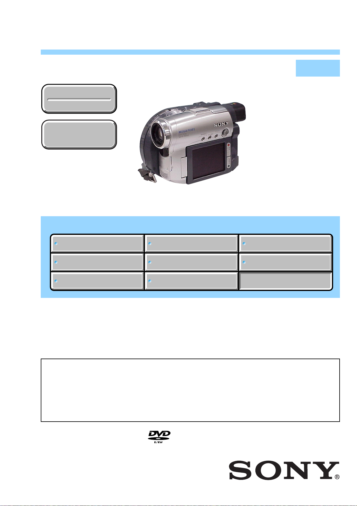
Photo : DCR-DVD201
Link
Link
SPECIFICATIONS
SPECIFICATIONS
BLOCK DIAGRAMS
BLOCK DIAGRAMS
LEVEL 2
DCR-DVD201
US Model
Canadian Model
Korea Model
Japanese Model
DCR-DVD201E
AEP Model
UK Model
East European Model
Australian Model
Chinese Model
Hong Kong Model
DCR-DVD201
DVD201E
E Model
Tourist Model
PRINTED WIRING BOARDS
PRINTED WIRING BOARDS
SERVICE NOTE
SERVICE NOTE
DISASSEMBLY
DISASSEMBLY
• For ADJUSTMENTS (SECTION 6), refer to SERVICE MANUAL, ADJ (987671551.pdf).
• For INSTRUCTION MANUAL, refer to SERVICE MANUAL, LEVEL 1 (987671541.pdf). (EXCEPT J MODEL)
• Since a service is provided only for the MD BLOCK ASSY (A-7113-371-A) and not for the single MD-104
board, complete.
• TO TAKE OUT A CASSETTE WHEN NOT EJECT (FORCE EJECT)
• Reference number search on printed wiring boards is available.
On the MD-104 board and VC-354 board
This service manual provides the information that is premised the circuit board replacement service and not intended repair
inside the MD-104 board and VC-354 board.
Therefore, schematic diagram, printed wiring board, wavef orms, mounted parts location and electrical parts list of the
board and VC-354
The following pages are not shown.
Disassembly...................................... Page 2-10
Schematic diagram ........................... Pages 4-31 to 4-82
Printed wiring board.......................... Pages 4-97 to 4-104
board are not shown.
FRAME SCHEMATIC DIAGRAMS
FRAME SCHEMATIC DIAGRAMS
SCHEMATIC DIAGRAMS
SCHEMATIC DIAGRAMS
Mounted parts location .........................
Exploded views....................................Pages 5-10 to 5-11
Electrical parts list................................Pages 5-17 to 5-30
REPAIR PARTS LIST
REPAIR PARTS LIST
Pages 4-106 to 4-108
MD-104
DIGITAL VIDEO CAMERA RECORDER
Page 2

Video camera
recorder
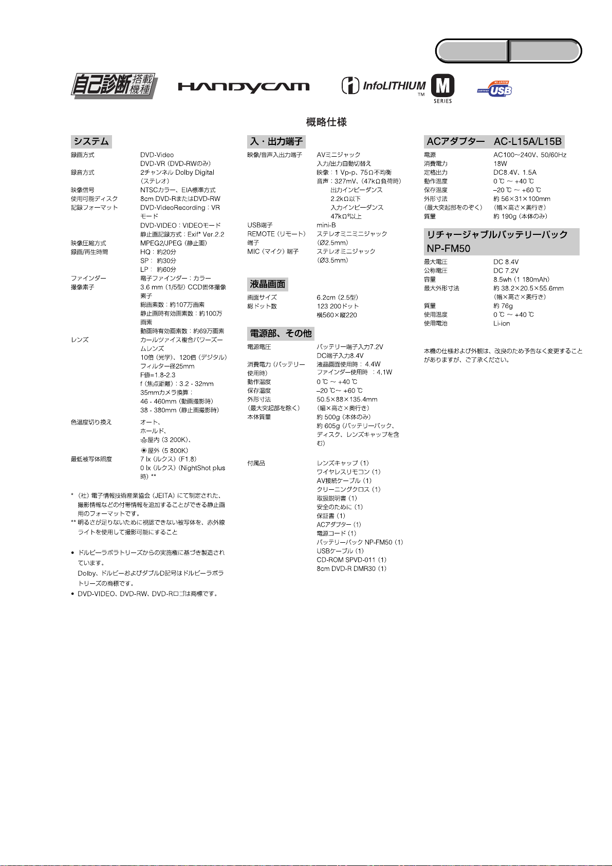
System
Video recording format
DVD-Video
DVD-VR (DVD-RW only)
Audio recording system
2ch Dolby* Digital
Video signal
DCR-DVD201:
NTSC color, EIA standards
DCR-DVD201E:
PAL color, CCIR standards
Usable discs
8 cm DVD-R and DVD-RW
Video compression format
MPEG2/JPEG (Still images)
Recording/playback time
HQ: Approx. 20 minutes
SP: Approx. 30 minutes
LP: Approx. 60 minutes
Viewfinder
Electric viewfinder (color)
Image device
3.6 mm (1/5 type) CCD (Charge
Coupled Device)
Number of Pixels
Gross: Approx. 1 070 000 pixels
Effective (for still images ):
Approx. 1 000 000 pixels
Effective (for movies):
Approx. 690 000 pixels
Lens
Carl Zeiss
Combined power zoom lens
Filter diameter:
25 mm (1 in.)
10× (Optical), 120× (Digital)
F = 1.8 – 2.3
* Manufactured under license
from Dolby Laboratories.
“Dolby” and the double-D
symbol are trademarks of Dolby
Laboratories.
SPECIFICATIONS
Focal length
3.2 – 32 mm (5/32 – 1 5/16 in.)
When converted to a 35 mm still
camera
For movies:
46 – 460 mm (1 7/8 – 18 1/8 in.)
For still images:
38 – 380 mm (1 1/2 – 15 in.)
Color temperature
Auto, HOLD (Hold), nIndoor
(3 200 K),
Minimum illumination
7 lx (lux) (F 1.8)
0 lx (lux) (in the NightShot Plus
mode)*
* Objects unable to be seen due to
the dark can be shot with
infrared lighting.
Input/Output connectors
AUDIO/VIDEO input/output
AV MINI JACK,
input/output autoswitch
Video : 1 Vp-p, 75 Ω (ohms),
unbalanced
Audio : 327 mV, (at output
impedance of more than 47 kΩ
(kilohms))
Output impedance of less than
2.2 kΩ (kilohms)
Input impedance of more than
47 kΩ (kilohms)
USB jack
mini-B
REMOTE jack
Stereo mini-minijack (ø 2.5 mm)
MIC jack
Stereo minijack (ø 3.5 mm)
LCD display
Picture
6.2 cm (2.5 type)
Total number of pixels
123 200 (560 × 220)
Outdoor (5 800 K)
General
Power requirements
7.2 V (battery pack)
8.4 V (AC adaptor)
Average power consumption
(when using the battery pack)
During camera recording using
LCD : 4.4 W
Viewfinder : 4.1 W
Operating temperature
0°C to 40°C (32°F to 104°F)
Storage temperature
–20°C to + 60°C
(–4°F to + 140°F)
Dimensions (Approx.)
DCR-DVD201:
50.5 × 88 × 135.4 mm
(2 1/4 × 3 1/2 × 5 3/8 in.)
(w/h/d)
DCR-DVD201E:
50.5 × 88 × 136 mm
(w/h/d)
Mass (approx.)
500 g
main unit only
605 g (15 oz)
including the battery pack,
disc and lens cap
Supplied accessories
See page 4.
DCR-DVD201/DVD201E
ENGLISH JAPANESE
ENGLISH JAPANESE
AC adaptor
AC-L15A/L15B
Power requirements
100 – 240 V AC, 50/60 Hz
Current consumption
0.35 – 0.18 A
Power consumption
18 W
Output voltage
DC OUT: 8.4 V, 1.5 A in the
operating mode
Operating temperature
0°C to 40°C (32°F to 104°F)
Storage temperature
–20°C to + 60°C (–4°F to + 140°F)
Dimensions (approx.)
56 × 31 × 100 mm
(2 1/4 × 1 1/4 ×
4 in.) (w/h/d)
excluding projecting parts
Mass (approx.)
190 g (6.7 oz)
excluding power cord
Rechargeable
battery pack
NP-FM50
Maximum output voltage
DC 8.4 V
Output voltage
DC 7.2 V
Capacity
8.5 Wh (1 180 mAh)
Dimensions (approx.)
38.2 × 20.5 × 55.6 mm
(1 9/16 × 13/16 × 2 1/4 in.)
(w/h/d)
Mass (approx.)
76 g (2.7 oz)
Operating temperature
0°C to 40°C (32°F to 104°F)
Type
Lithium ion
Design and specifications are
subject to change without notice.
— 2 —
Page 3
DCR-DVD201/DVD201E
ENGLISH JAPANESE
ENGLISH JAPANESE
— 3 —
Page 4
SAFETY CHECK-OUT
After correcting the original service problem, perform the following
safety checks before releasing the set to the customer.
DCR-DVD201/DVD201E
ENGLISH JAPANESE
ENGLISH JAPANESE
1. Check the area of your repair for unsoldered or poorly-soldered
connections. Check the entire board surface for solder splashes
and bridges.
2. Check the interboard wiring to ensure that no wires are
"pinched" or contact high-wattage resistors.
3. Look for unauthorized replacement parts, particularly
transistors, that were installed during a previous repair . Point
them out to the customer and recommend their replacement.
4. Look for parts which, through functioning, show obvious signs
of deterioration. Point them out to the customer and
recommend their replacement.
5. Check the B+ voltage to see it is at the values specified.
6. Flexible Circuit Board Repairing
• Keep the temperature of the soldering iron around 270˚C
during repairing.
• Do not touch the soldering iron on the same conductor of the
circuit board (within 3 times).
• Be careful not to apply force on the conductor when soldering
or unsoldering.
SAFETY-RELATED COMPONENT WARNING!!
COMPONENTS IDENTIFIED BY MARK 0 OR DOTTED LINE WITH
MARK 0 ON THE SCHEMATIC DIAGRAMS AND IN THE PARTS
LIST ARE CRITICAL TO SAFE OPERATION. REPLACE THESE
COMPONENTS WITH SONY PARTS WHOSE PART NUMBERS
APPEAR AS SHOWN IN THIS MANUAL OR IN SUPPLEMENTS
PUBLISHED BY SONY .
Unleaded solder
Boards requiring use of unleaded solder are printed with the leadfree mark (LF) indicating the solder contains no lead.
(Caution: Some printed circuit boards may not come printed with
the lead free mark due to their particular size.)
: LEAD FREE MARK
Unleaded solder has the following characteristics.
• Unleaded solder melts at a temperature about 40°C higher than
ordinary solder.
Ordinary soldering irons can be used but the iron tip has to be
applied to the solder joint for a slightly longer time.
Soldering irons using a temperature regulator should be set to
about 350°C.
Caution: The printed pattern (copper foil) may peel away if the
heated tip is applied for too long, so be careful!
• Strong viscosity
Unleaded solder is more viscous (sticky , less pr one to flo w) than
ordinary solder so use caution not to let solder bridges occur such
as on IC pins, etc.
• Usable with ordinary solder
It is best to use only unleaded solder but unleaded solder may
also be added to ordinary solder.
ATTENTION AU COMPOSANT AYANT RAPPORT
À LA SÉCURITÉ!
LES COMPOSANTS IDENTIFÉS P AR UNE MARQUE 0 SUR LES
DIAGRAMMES SCHÉMA TIQUES ET LA LISTE DES PIÈCES SONT
CRITIQUES POUR LA SÉCURITÉ DE FONCTIONNEMENT. NE
REMPLACER CES COMPOSANTS QUE PAR DES PIÈSES SONY
DONT LES NUMÉROS SONT DONNÉS DANS CE MANUEL OU
DANS LES SUPPÉMENTS PUBLIÉS PAR SONY.
CAUTION :
Danger of explosion if battery is incorrectly replaced.
Replace only with the same or equivalent type.
WARNING!!
WHEN SERVICING, DO NOT APPRO ACH THE LASER
EXIT WITH THE EYE TOO CLOSELY. IN CASE IT IS
NECESSARY TO CONFIRM LASER BEAM EMISSION,
BE SURE TO OBSER VE FR OM A DIST ANCE OF MORE
THAN 30 cm FROM THE SURFACE OF THE
OBJECTIVE LENS ON THE OPTICAL PICK-UP BLOCK.
CAUTION:
The use of optical instrument with this product will increase eye
hazard.
CAUTION
Use of controls or adjustments or performance
procedures other than those specified herein may
result in hazardous radiation exposure.
— 4 —
Page 5
DCR-DVD201/DVD201E
ENGLISH JAPANESE
ENGLISH JAPANESE
— 5 —
Page 6

DCR-DVD201/DVD201E
TABLE OF CONTENTS
1. SERVICE NOTE
1-1. SER VICE NOTE ·····························································1-1
1. NOTE FOR REPAIR ·······················································1-1
2. POWER SUPPLY DURING REPAIRS ·························· 1-2
3. TO TAKE OUT A CASSETTE WHEN NOT EJECT
(FORCE EJECT) ·····························································1-2
4. NOTES ON HANDLING THE OPTICAL PICK-UP ····1-2
5. PRECAUTION FOR CHECKING EMISSION
OF LASER DIODE·························································1-2
1-2. SELF-DIAGNOSIS FUNCTION····································1-3
1. SELF-DIAGNOSIS FUNCTION····································1-3
2. SELF-DIAGNOSIS DISPLAY ······································· 1-3
3. SELF-DIAGNOSIS CODE TABLE································1-3
2. DISASSEMBLY
2-1. DISASSEMBLY······························································ 2-1
2-2. SERVICE POSITION ····················································· 2-5
2-3. CIRCUIT BOARDS LOCATION ···································2-8
2-4. FLEXIBLE BOARDS LOCATION ································2-9
Disassembling procedure of MD block assembly is
not shown. Page 2-10 is not shown.
HELP (List of caution points is shown here.)
3. BLOCK DIAGRAMS
3-1. OVERALL BLOCK DIAGRAM (1/4) ··························· 3-1
3-2. OVERALL BLOCK DIAGRAM (2/4) ··························· 3-3
3-3. OVERALL BLOCK DIAGRAM (3/4) ··························· 3-5
3-4. OVERALL BLOCK DIAGRAM (4/4) ··························· 3-7
3-5. POWER BLOCK DIAGRAM (1/3)································3-9
3-6. POWER BLOCK DIAGRAM (2/3)······························3-11
3-7. POWER BLOCK DIAGRAM (3/3)······························3-13
4. PRINTED WIRING BOARDS AND
SCHEMATIC DIAGRAMS
4-1. FRAME SCHEMATIC DIAGRAM (1/3)······················· 4-1
FRAME SCHEMATIC DIAGRAM (2/3)······················· 4-3
FRAME SCHEMATIC DIAGRAM (3/3)······················· 4-5
4-2. SCHEMATIC DIAGRAMS
• CD-504 (CCD IMAGER)
SCHEMATIC DIAGRAM ····························4-11
• FP-884 (LITHIUM BATTERY, SW)
SCHEMATIC DIAGRAM ····························4-13
• FP-887 (USB JACK) FLEXIBLE
SCHEMATIC DIAGRAM ····························4-15
• FP-890 (PANEL REV SW) FLEXIBLE
SCHEMATIC DIAGRAM ····························4-15
• FP-891 (EJECT MOTOR, SW) FLEXIBLE
SCHEMATIC DIAGRAM ····························4-17
• LB-107 (EVF I/F, BACK LIGHT)
SCHEMATIC DIAGRAM ····························4-17
• JS-030 (KEY I/F)
SCHEMATIC DIAGRAM ····························4-19
• MA-429 (MIC, REMOTE SENSOR, MULTI AV JACK)
SCHEMATIC DIAGRAM ····························4-21
• SE-143 (PITCH/YAW SENSOR)
SCHEMATIC DIAGRAM ····························4-23
• PD-220 (LCD DRIVE)
SCHEMATIC DIAGRAM ····························4-25
• CONTROL SWITCH BLOCK (BL8700, PS8700)
SCHEMATIC DIAGRAM ····························4-27
• CONTROL SWITCH BLOCK (SH8700)
SCHEMATIC DIAGRAM ····························4-29
4-3. PRINTED WIRING BOARDS
• CD-504 (CCD IMAGER)
PRINTED WIRING BOARD ·······················4-85
• FP-890 (PANEL REV SW)
PRINTED WIRING BOARD ·······················4-87
• FP-884 (LITHIUM BATTERY, SW) FLEXIBLE
PRINTED WIRING BOARD ·······················4-88
• JS-030 (KEY I/F)
PRINTED WIRING BOARD ·······················4-89
• MA-429 (MIC, REMOTE SENSOR, MULTI AV JACK)
PRINTED WIRING BOARD ·······················4-91
• PD-220 (LCD DRIVE)
PRINTED WIRING BOARD ·······················4-93
• LB-107 (EVF I/F, BACK LIGHT)
PRINTED WIRING BOARD ·······················4-95
• SE-143 (PITCH/YAW SENSOR)
PRINTED WIRING BOARD ·······················4-95
Printed wiring board of the MD-104 board and VC-354
are not shown.
Pages from 4-97 to 4-104 are not shown.
4-4. MOUNTED PARTS LOCATION ······························· 4-105
Mounted parts location of the MD-104 board and
VC-354 are not shown.
Pages from 4-106 to 4-108 are not shown.
5. REPAIR PARTS LIST
5-1. EXPLODED VIEWS ······················································5-3
5-1-1.OVERALL SECTION·····················································5-3
5-1-2.CABINET (R) SECTION ···············································5-4
5-1-3.LCD SECTION ·······························································5-5
5-1-4.EVF SECTION································································5-6
5-1-5.LENS SECTION ·····························································5-7
5-1-6.CABINET (L) SECTION················································5-8
5-1-7.D LID SECTION·····························································5-9
Exploded view and parts list of MD BLOCK are not
shown. Pages 5-10 and 5-11 are not shown.
Checking supplied accessories. ····································· 5-12
5-2. ELECTRICAL PARTS LIST ········································5-14
Electrical parts list of the MD-104 board and
VC-354 board are not shown.
Pages from 5-17 to 5-30 are not shown.
Shematic diagram of the MD-104 board and VC-354
are not shown.
Pages from 4-31 to 4-82 are not shown.
— 6 —
Page 7
DCR-DVD201/DVD201E
SECTION 1
SERVICE NOTE
1-1. SERVICE NOTE
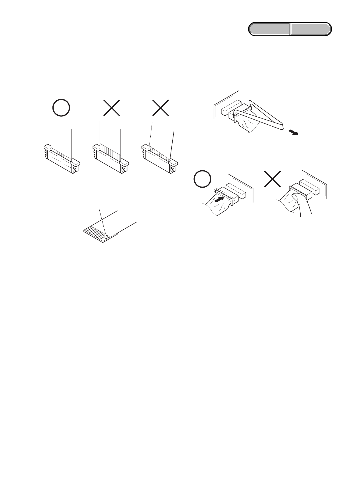
1. NOTE FOR REPAIR
Make sure that the flat cable and flexible board are not cracked of
bent at the terminal.
Do not insert the cable insufficiently nor crookedly.
Cut and remove the part of gilt
which comes off at the point.
(Take care that there are
some pieces of gilt left inside)
ENGLISH JAPANESE
ENGLISH JAPANESE
When remove a connector, don't pull at wire of connector.
Be in danger of the snapping of a wire.
When installing a connector, don't press down at wire of connector.
Be in danger of the snapping of a wire.
1-1
Page 8
DCR-DVD201/DVD201E
ENGLISH JAPANESE
ENGLISH JAPANESE
2. POWER SUPPLY DURING REPAIRS
In this unit, about 10 seconds after power is supplied to the battery terminal using the regulated power supply (8.4V), the po wer is shut of f so
that the unit cannot operate.
This following two methods are available to prevent this. Take note of which to use during repairs.
Method 1.
Use the AC power adaptor.
Method 2.
Connect the servicing remote commander RM-95 (J-6082-053-B) to the LANC jack, and set the commander switch to the “ADJ” side.
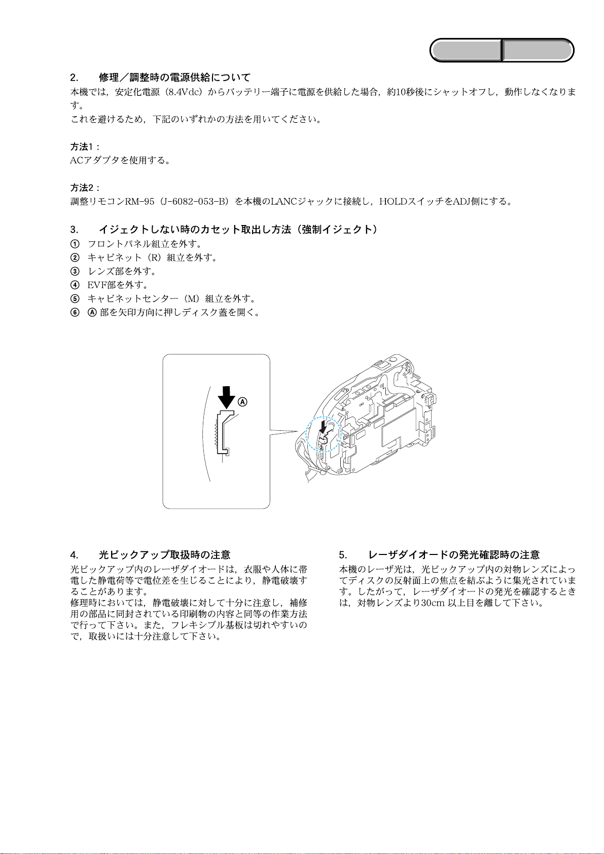
3. TO TAKE OUT A CASSETTE WHEN NOT EJECT (FORCE EJECT)
1 Remove the front panel assembly.
2 Remove the cabinet (R) assembly.
3 Remove the lens block.
4 Remove the EVF block.
5 Remove the cabinet center (M) assembly.
6 Push the portion A in the direction of the arrow and open the disc cover.
A
4.
NOTES ON HANDLING THE OPTICAL PICK-UP
The laser diode may suffer electrostatic breakdown because of the
potential difference generated by the charged electrostatic load, etc.
on clothing and the human body.
During repair, pay attention to electrostatic breakdown and also use
the procedure in the printed matter which is included in the repair
parts.
The flexible board is easily damaged and should be handled with
care.
5. PRECAUTION FOR CHECKING EMISSION OF
LASER DIODE
Laser light of the equipment is focused by the object lens in the
optical pick-up so that the light focuses on the reflection surface of
the disc. Therefore, be sure to keep your eyes more then 30 cm
apart from the object lens when you check the emission of laser
diode.
1-2
Page 9
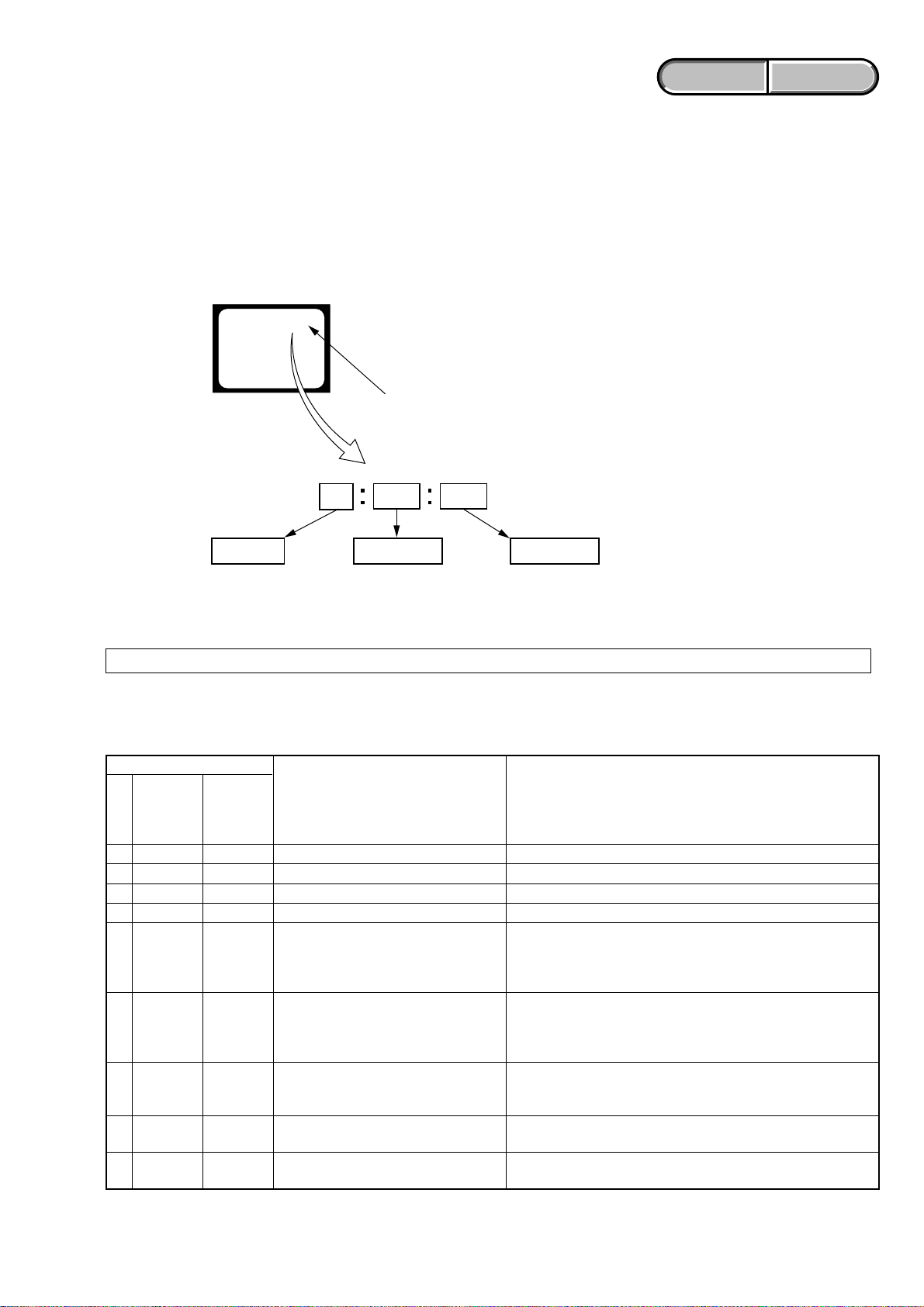
1-2. SELF-DIAGNOSIS FUNCTION
1. SELF-DIAGNOSIS FUNCTION
When problems occur while the unit is operating, the self-diagnosis
function starts working, and displays on the viewfinder, or LCD
screen what to do. This function consists of two display; selfdiagnosis display and service mode display.
Details of the self-diagnosis functions are provided in the Instruction
manual.
Viewfinder or LCD screen
C : 1 3 : 0 0
Blinks at 3.2Hz
DCR-DVD201/DVD201E
ENGLISH JAPANESE
ENGLISH JAPANESE
2. SELF-DIAGNOSIS DISPLAY
When problems occur while the unit is operating, the counter of the
viewfinder or LCD screen consists of an alphabet and 4-digit number ,
which blinks at 3.2Hz. This 5-character display indicates the
“repaired by:”, “block” in which the problem occurred, and “detailed
code” of the problem.
1 3C
Repaired by:
C : Corrected by customer
H : Corrected by dealer
E : Corrected by service
engineer
Note: The “self-diagnosis display” data will be kept even if the lithium battery (FP-884 flexible board BT5201 of the cabinet (R) assembly) is removed.
Indicates the appropriate
step to be taken.
E.g.
13....Faulty disc is used.
Block
0 0
Detailed Code
Self-diagnosis Code Table.
3. SELF-DIAGNOSIS CODE TABLE
Self-diagnosis Code
Repaired by:
C
C
C
E
E
E
E
E
E
Block
Function
04
13
21
20
61
61
62
93
94
Detailed
Code
00
00
00
00
00
10
00
00
01
Symptom/State
Non-standard battery is used.
Faulty disc is used.
Condensation.
EEPROM data are rewritten.
Difficult to adjust focus
(Cannot initialize focus.)
Zoom operations fault
(Cannot initialize zoom lens.)
Handshake correction function does not
work well. (With pitch angular velocity
sensor output stopped.)
USB bridge IC fault
Fault of writing to or erasing the flash
memory
Correction
Use the InfoLITHIUM battery.
Use a compatible disc with the camcorder.
Remove the disc, and insert it again after one hour.
Make EEPROM data correct value. (Note)
Inspect the lens block focus MR sensor (Pin 1, 2 of CN1501 of
VC-354 board) when focusing is performed when the control button
is pressed in the focus manual mode and inspect the focus motor drive
circuit (IC1501 of VC-354 board) when the focusing is not perf ormed.
Inspect the lens block zoom reset sensor (Pin wh of CN1501 of
VC-354 board) when zooming is performed when the zoom switch
is pressed and inspect the zoom motor drive circuit (IC1501 of
VC-354 board) when the zooming is not performed.
Inspect angular velocity sensors (SE5501, 5502 of SE-143
board) peripheral circuits.
Inspect the USB bridge IC (MD-104 board IC4201) and EEPROM
(MD-104 board IC4200)
Inspect the flash memory (VC-354 board IC3401) (Note)
Note: Refer to “9. Record of Self-diagnosis check” of “6-3. SERVICE
MODE”, ADJ (987671551.pdf).
1-3
Page 10
DCR-DVD201/DVD201E
SECTION 1
SERVICE NOTE
ENGLISH JAPANESE
ENGLISH JAPANESE
1-4
Page 11
DCR-DVD201/DVD201E
ENGLISH JAPANESE
ENGLISH JAPANESE
1-5
Page 12
DCR-DVD201/DVD201E
ENGLISH JAPANESE
ENGLISH JAPANESE
1-6E
Page 13
SECTION 2
DISASSEMBLY
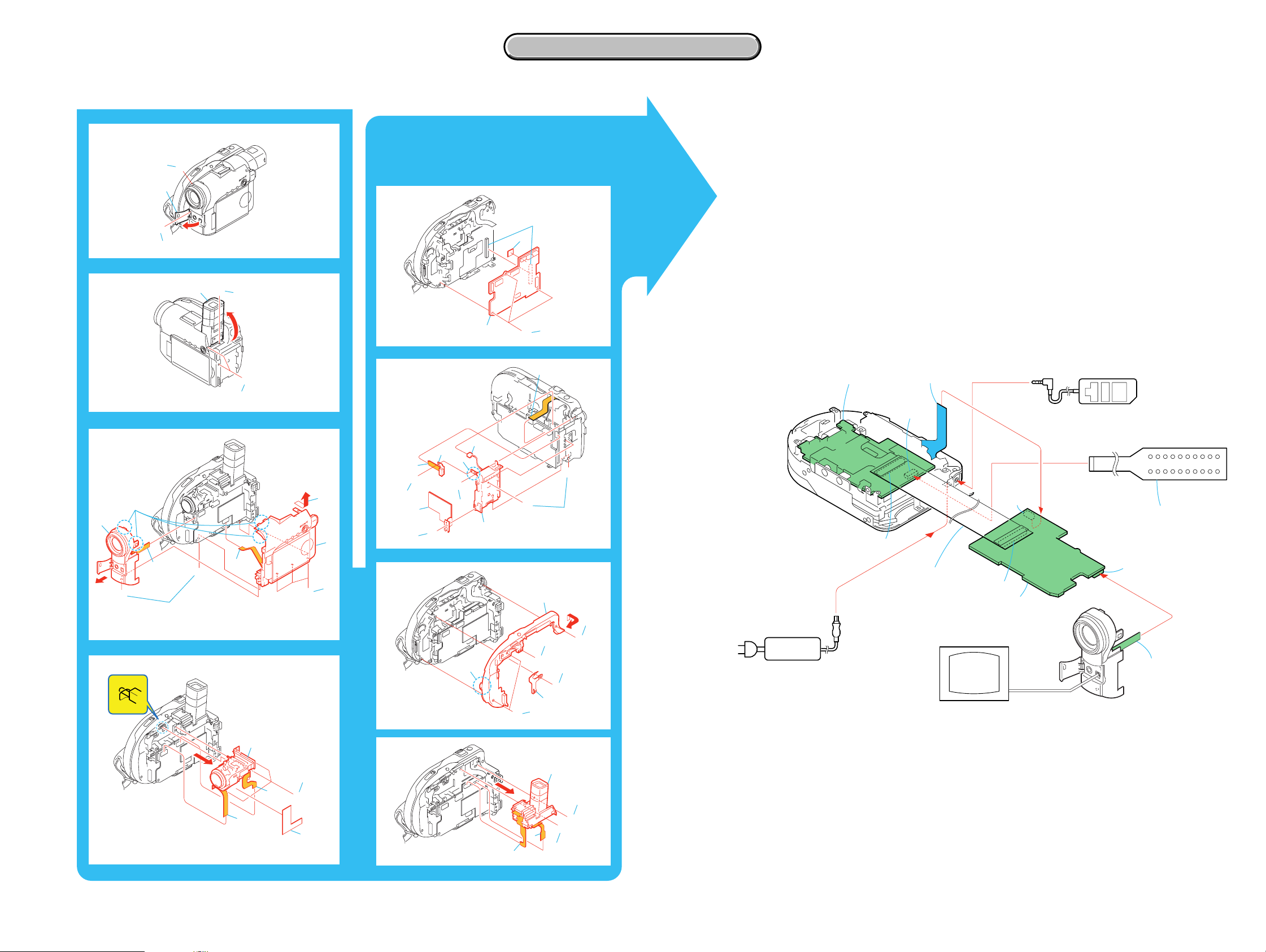
The following flow chart shows the disassembly procedure.
2-1. DISASSEMBLY
3
B
DCR-DVD201/DVD201E
4
B
5
HELP 01
5
7
3
1
A
1
Two grip screws (M1.7x3) black
2
Two grip screws (M1.7x3) black
3
Six claws
4
P cabinet (C) assembly
5
Sheet (MY)
C
1
1
B
2
1
Open the jack cover
2
EG grip Screw (M1.7x4) black
3
EG grip Screw (M1.7x4) black
9
4
qs
4
Turn over the EVF section in the
direction of the arrow.
5
EG grip Screw (M1.7x4) black
6
Two EG grip Screws (M1.7x4) black
A
2
5
qa
qd
B
6
1
Screw (M1.7x2.5) silver
2
EG grip screw (M1.7x4) black
3
FP-883 flexible board (10P)
4
FP-889 flexible board (20P)
5
EVF section
0
qf
4
3
5
B
7
B
8
7
Three EG grip Screws (M1.7x4) black
8
Two EG grip Screws (M1.7x4) black
9
Five claws
7
4
5
2
0
Remove the cabinet (R) section
in the direction of the arrow.
qa
MA-429 board (27P)
qs
F panel section
qd
FP-884 flexible board (33P)
qf
Cabinet (R) section
B
B
C
3
6
B
4
1
T ape (0915)
2
Three screws (M1.7x2.5) silver
3
FP-892 flexible board (39P)
4
From lens flexible board (29P)
5
Lens section
qa
qs
9
0
7
2
A
5
6
A
E
8
1
4
3
2
B
D
1
2
3
D
1
4
5
6
6
2
a
b
1
VC-354
D
1
4
5
3
A
2
HELP 02
7
D
3
2
1
4
D
2
5
E
1
Screw (M1.7x2.5) silver
2
VC heat sink, VC radiation sheet,
VC insulating sheet
3
Three screws (M1.7x2.5) silver
4
Control switch block (PS8700) (20P)
5
Board to board (CN1007, CN4901) (100P)
6
Radiation sheet (135)
7
VC-354 board
3
B
1
See page
2-3.
D
1
Screw (M1.7x2.5) silver
2
Front fixed plate
3
EG grip screw (M1.7x4) black
4
Screw (M1.7x2.5) silver
5
Two tapping screws (M1.7x5) black
6
Claw
7
Remove the cabinet center (M)
assembly in the direction of the arrow.
1
Push this portion with a finger
in the direction of the arrow a.
2
Open the D lid assembly
in the direction of the arrow b.
A
Screw
M1.7x3
3-084-817-21
C
B
Screw
M1.7x4
3-087-376-01
D
1
Two tapping screws (M1.7x3.5) silver
2
Speaker retainer plate assembly
3
Three tapping screws (M1.7x3.5) silver
4
FP-890 board (20P)
5
FP-884 flexible board (8P)
6
Three EG grip screws (M1.7x4) black
7
LCD section
2-1 2-2
1
Two grip screws (M1.7x3) black
2
Two grip screws (M1.7x3) black
3
Six claws
4
P cabinet (C) assembly
5
FP-890 board (22P)
6
Hinge (87) assembly, Hinge cover (O),
Hinge cover (U), FP-890 board
7
Sheet (MY)
8
Screw (M1.7x5) black
9
Control switch block (BL8700) (6P)
0
T wo claws
qa
P cabinet (M) assembly
qs
PD-220 board, Insulating sheet,
Light guide plate block
1
Grip screw (M1.7x3) black
2
Four claws
3
Hinge cover (O)
4
Hinge cover (U)
5
Hinge (87) assembly, FP-890 board
Tapping screw
M1.7x3.5
3-078-890-01
E
Tapping screw
M1.7x5
3-081-204-21
Screw
M1.7x2.5
3-078-889-11
Silver
Black
Page 14
DCR-DVD201/DVD201E
VC-354
8
qa
D
D
4
5
9
B
0
D
3
2
1
1
Screw (M1.7x2.5) silver
2
VC heat sink, VC radiation sheet,
VC insulating sheet
3
Screw (M1.7x2.5) silver
4
Claw
5
Screw (M1.7x2.5) silver
7
B
6
6
Two EG grip screws (M1.7x4) black
7
Control switch block (PS8700) (20P)
8
Battery terminal board (3P)
9
Battery terminal board
0
FP-887 flexible board (8P)
qa
Square type connector (USB 5P),
FP-887 flexible board
2
E
1
1
Two tapping screws (M1.7x5) black
2
Remove the D lid assembly
in the direction of the arrow.
2
3
VC-354
4
1
Three screws (M1.7x2.5) silver
2
Board to board (CN1007,CN4901) (100P)
3
Radiation sheet (135)
4
VC-354 board
1
D
3
c
b
2
a
1
1
Remove the grip belt
in the direction of the arrow a.
2
Push this portion with a finger
in the direction of the arrow b.
3
Open the D lid assembly
in the direction of the arrow c.
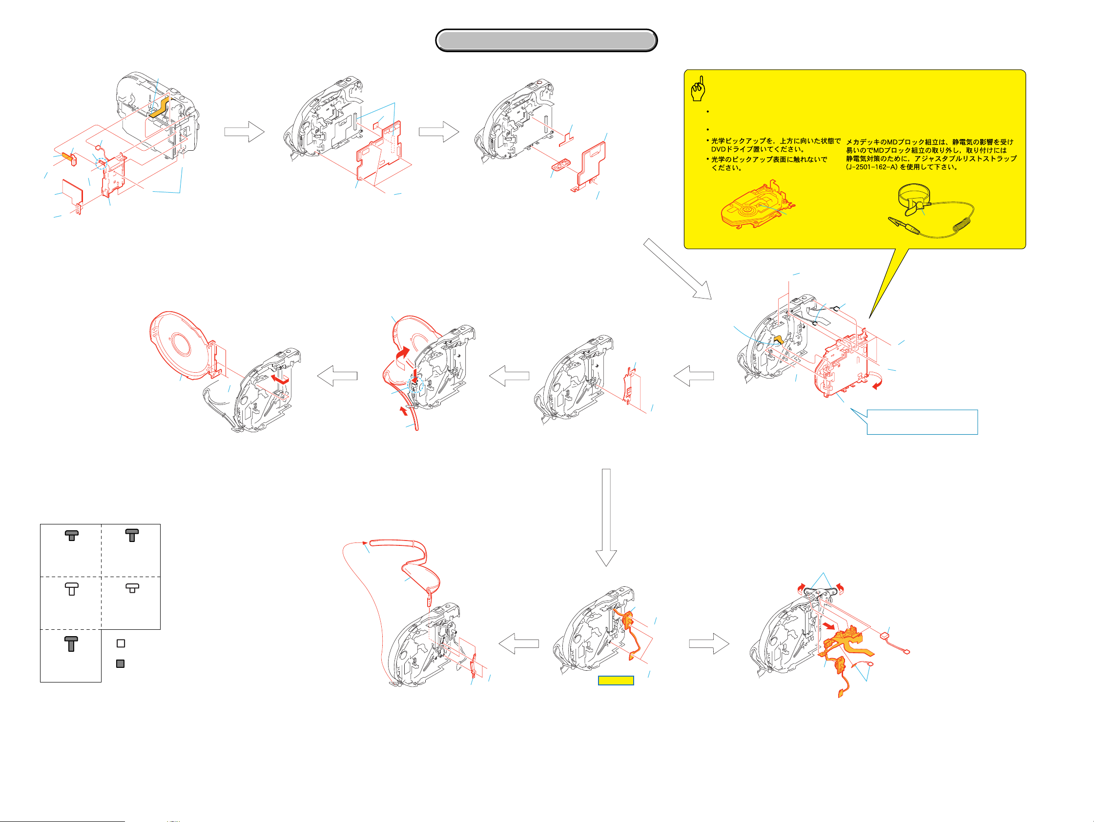
2. DISASSEMBLY
2. DISASSEMBLY
4
2
MD-104
3
1
Screw (M1.7x2.5) silver
2
VM heat sink, VM radiation sheet, VM insulating sheet
3
T ripod large
4
Sheet radiation (2345)
1
Two tapping screws (M1.7x5) black
2
D blind plate assembly
D
1
Caution
Precautions during handling
Be sure to place the DVD drive with its
optical pickup facing upward.
Do not touch the optical pickup surface.
Optical pickup
1
D
7
Use the adjustable wrist strap (J-2501-162-A) as the
preventive measure for static electricity when the
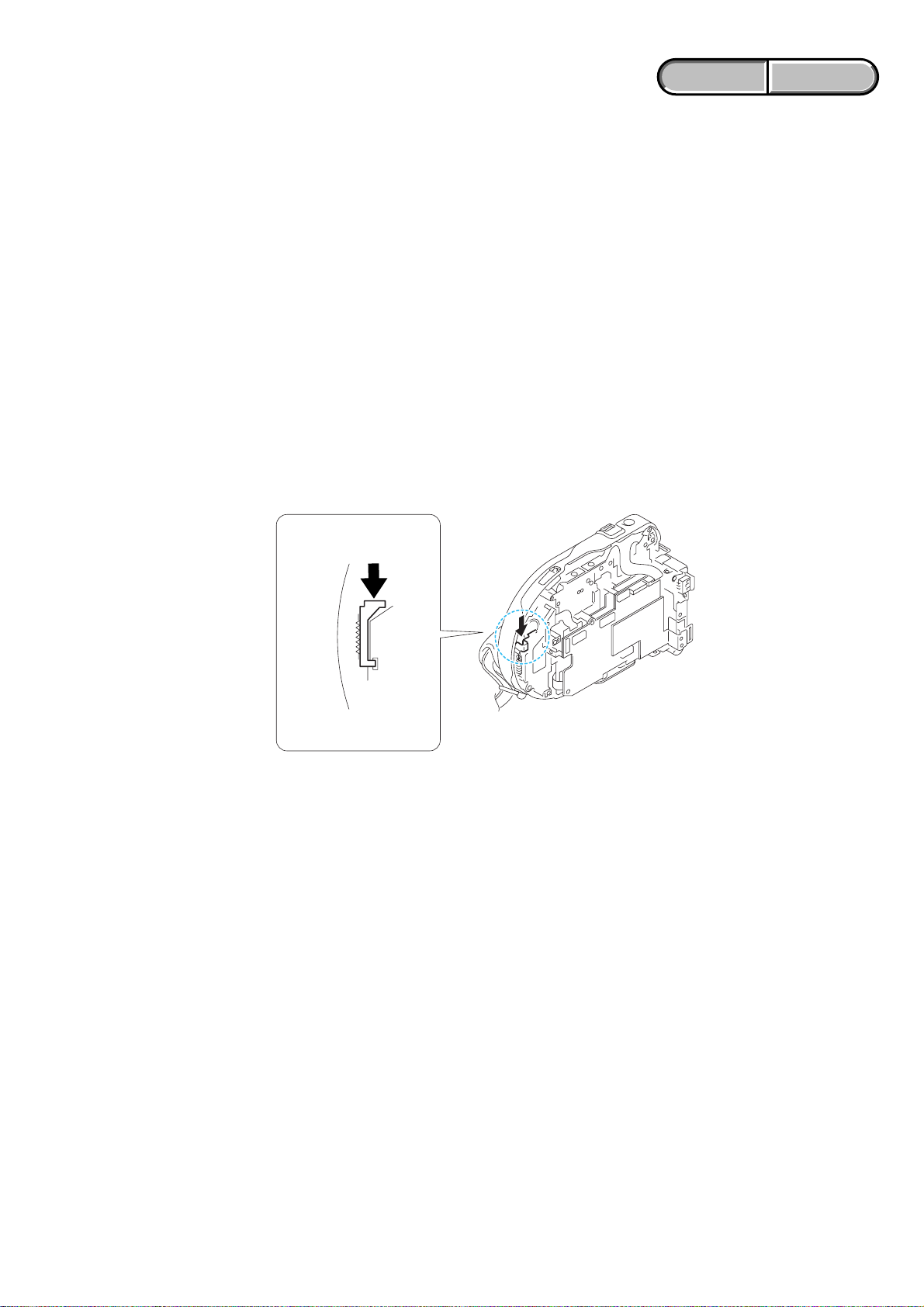
removing and installing the MD black assembly because
the MD black assembly of this mechanism beck is easily
affected by the static electricity.
(J-2501-162-A)
56
3
E
2
C
4
Refer to level 3
Disassembling procedure of
MD block assembly.
5
DC-IN connector inlet (3P)
6
Harness (DM-144) (2P) (Dew sensor)
7
FP-891 flexible board (10P)
8
Remove the MD block assembly in the
direction of the arrow.
E
D
2
1
1
Two screws (M1.7x2.5) silver
2
Screw (M1.7x2.5) silver
3
Three tapping screws (M1.7x5) black
4
Tapping screw (M1.7x3.5) silver
MD-104
8
A
Screw
M1.7x3
3-084-817-21
C
Tapping screw
M1.7x3.5
3-078-890-01
E
Tapping screw
M1.7x5
3-081-204-21
B
Screw
M1.7x4
3-087-376-01
D
Screw
M1.7x2.5
3-078-889-11
Silver
Black
1
4
3
2
C
3
1
Remove the grip belt
in the direction of the arrow.
2
Two tapping screw (M1.7x3.5) silver
3
Grip belt sheet metal (Rear)
4
Grip belt
2
C
HELP 03
1
Two tapping screws (M1.7x5) black
2
Tapping screw (M1.7x3.5) silver
3
Control switch block (PS8700)
1
E
1
Open the jack cover (DC) in the directions of the arrows a and b.
2
DC-IN connector inlet
3
Harness (DM-144), FP-228 flexible board (Dew senser)
4
Control switch block (PS8700)
2-3 2-4
1
ab
2
4
3
Page 15
2-2. SERVICE POSITION
3
B
1
B
2
4
B
DCR-DVD201/DVD201E
2. DISASSEMBLY
2. DISASSEMBLY
[SERVICE POSITION TO CHECK THE DVD DRIVE SECTION]
Connection to Check the DVD drive section
To check the DVD drive section, set the DVD drive to PLAY mode. (Set the mode dial to PLAY position,
or set forced PLAY mode by using the adjustment remote commander.)
Operate the DVD drive using the adjustment remote commander (with the HOLD switch set in the OFF position).
2
3
5
VC-354
Note: Removing the control switch block (PS8700) means removing the LID OPEN switch. Therefore the DVD
drive section will not move even if the forced PLAY mode is set up.
Setting the forced PLAY mode
1) Select page: 0, address: 01, and set data: 01.
2) Select page: 0, address: 10, and set data: 00.
3) Select page: D, address: 10, set data: 02, and press the
PAUSE button of the adjustment remote commander.
Exiting the forced PLAY mode
1) Select page: 0, address: 01, and set data: 01.
2) Select page: 0, address: 10, and set data: 00.
3)
Select page: D, address: 10, set data: 00, and press the
PAUSE button of the adjustment remote commander.
4) Select page: 0, address: 01, and set data: 00.
4
B
6
8
qa
D
4
D
5
9
0
D
9
qs
qa
qd
0
qf
3
2
1
B
7
B
8
B
6
D
VC-354
B
7
D
1
Adjustment remote
commander (RM-95)
MD-104 board
Control switch block
(PS8700) (20P)
CN4902
LANC
MD-104
B
6
CN4901
Extension cable (100P)
(J-6082-352-A)
7
3
B
4
1
AC IN
AC power
adaptor
DC-IN
CN1001
CPC-8 jig
(J-6082-388-A)
VC-354
CN1006
CN1007
VC-354 board
MA-429 board
D
AUDIO/
VIDEO jack
E
2
5
Monitor TV
5
2
3
D
4
1
3
5
2
B
D
4
1
2-5 2-6
Page 16
DCR-DVD201/DVD201E
N
2. DISASSEMBLY
2. DISASSEMBLY
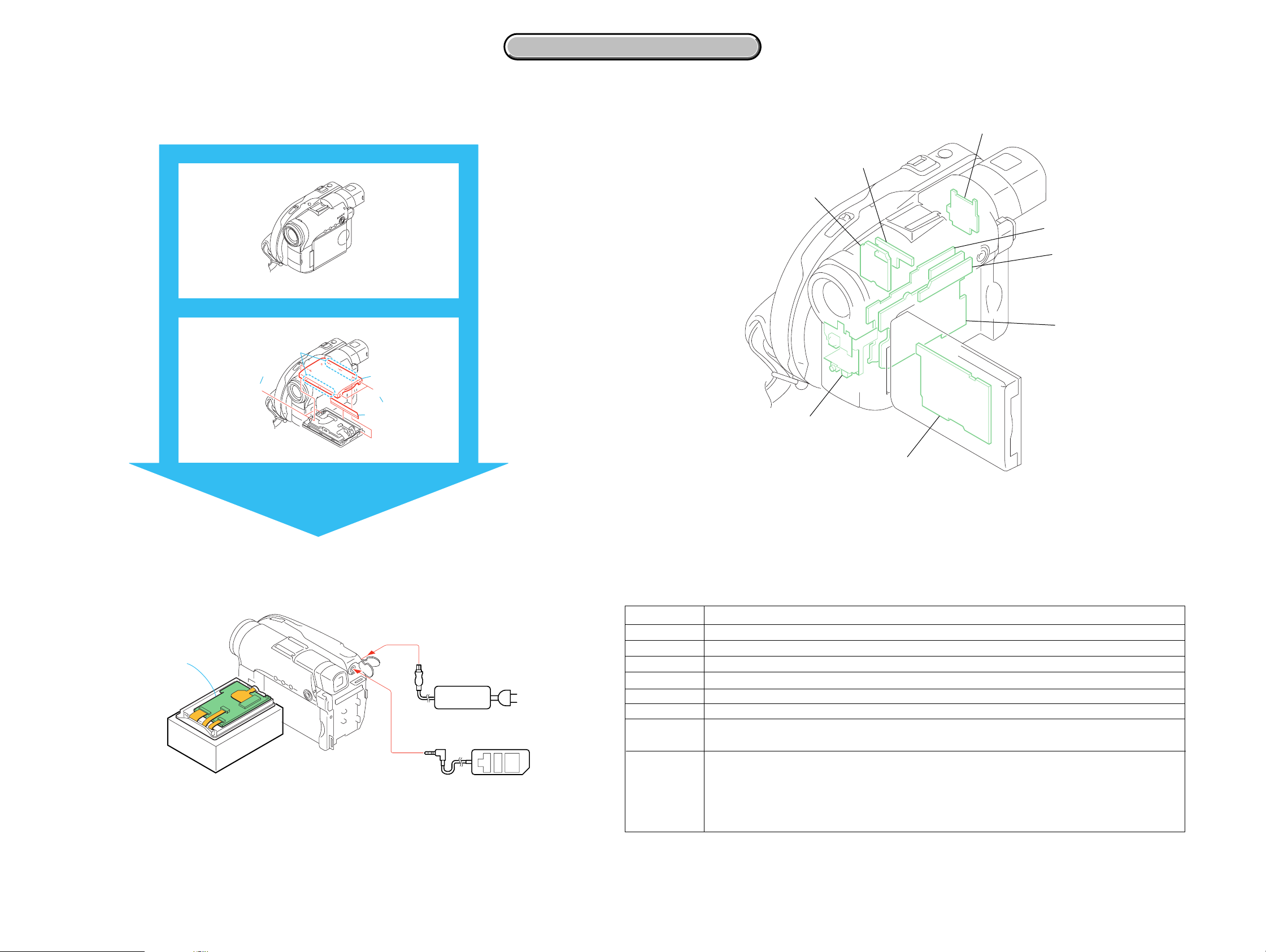
2-3. CIRCUIT BOARDS LOCATION
[PD-220 BOARD SERVICE POSITION]
A
LB-107
SE-143
CD-504
MD-104
JS-030
VC-354
3
1
4
A
2
5
MA-429
PD-220 board
PD-220
LANC
AC power
adaptor
Adjustment remote
commander (RM-95)
AC I
NAME
CD-504
JS-030
PD-220
LB-107
MA-429
SE-143
MD-104
VC-354
PD-220
FUNCTION
CCD IMAGER
KEY I/F
LCD DRIVE
EVF I/F, BACKLIGHT
MIC, REMOTE SENSOR, MULTI AV JACK
PITCH/YAW SENSOR
RF PROCESS, DVD DSP, MECHA DRIVE, MICRO COMPUTER, FLASH, LATCH, USB I/F,
SHOCK SENSOR, CONNECTOR, DC/DC CONVERTER
A/D CONV., TIMING GENERATOR, CAMERA PROCESS, LENS DRIVE,
DVD SYSTEM CONTROL, 128M SDRAM, 16M FCRAM, DVD CODEC,
64M SDRAM, VIDEO IN/OUT, VIDEO A/D CONVERTER, EVF DRIVE, CAMERA CONTROL,
HI CONTROL, HI/ DIGITAL STILL CONTROL, 32M FLASH MEMORY, AUDIO I/O, MIC AMP,
PITCH/YAW SENSOR AMP, CONNECTOR, DD CONNECTOR
2-7 2-8
Page 17
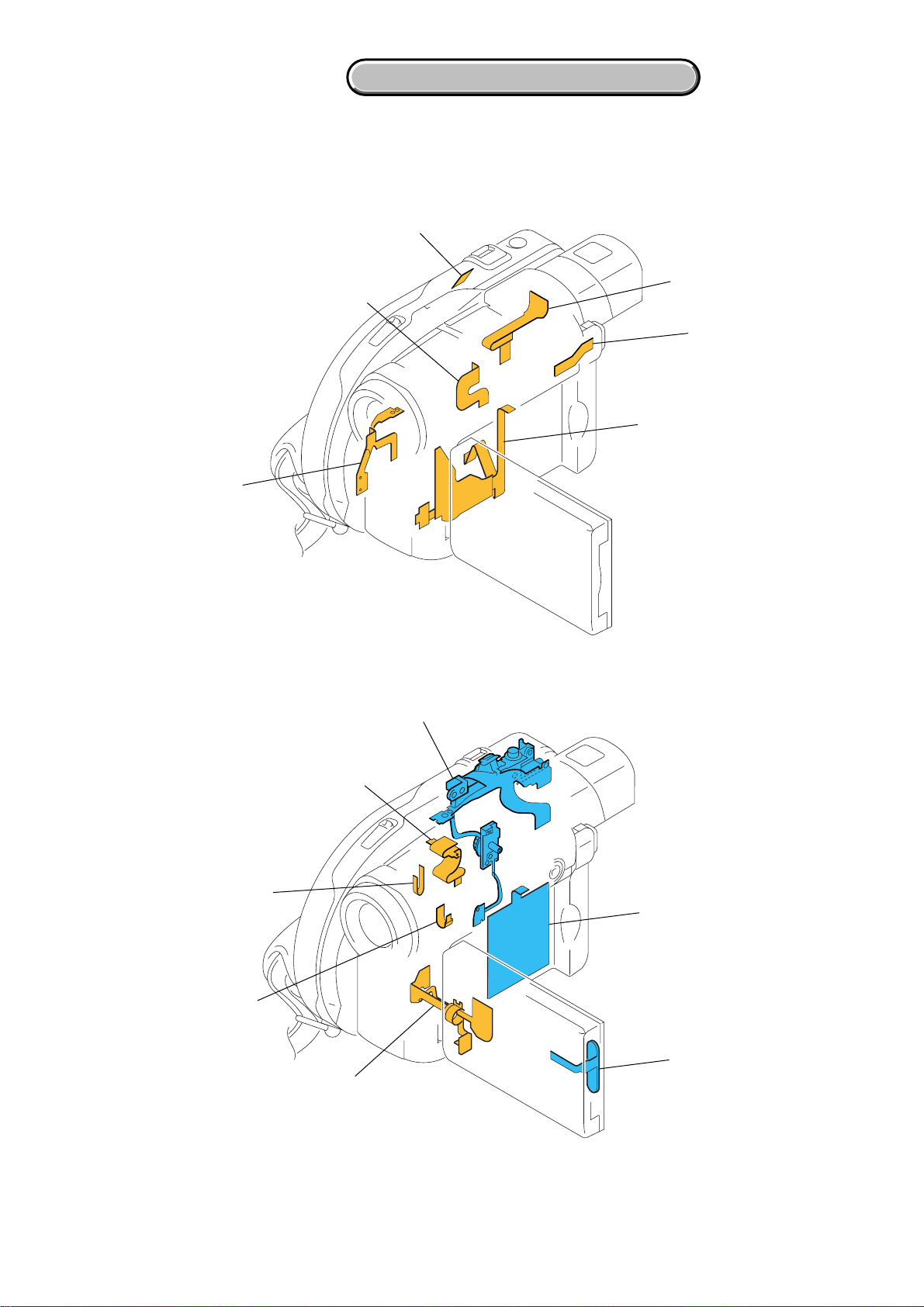
2-4. FLEXIBLE BOARDS LOCATION
The flexible boards contained in the lens block is not shown.
FP-228
2. DISASSEMBLY
2. DISASSEMBLY
DCR-DVD201/DV201E
FP-891
FP-892
FP-889
FP-887
FP-884
CONTROL SWTICH BLOCK (PS8700)
FP-888
FP-629
FP-883
FP-890
CONTROL SWTICH
BLOCK (SH8700)
CONTROL SWTICH
BLOCK (BL8700)
2-9E
Page 18

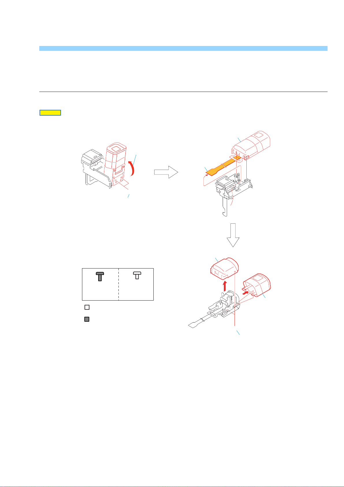
Disassembling procedure of MD bloc k
assembly are not shown.
Page 2-10 is not shown.
Page 19
DCR-DVD201/DVD201E
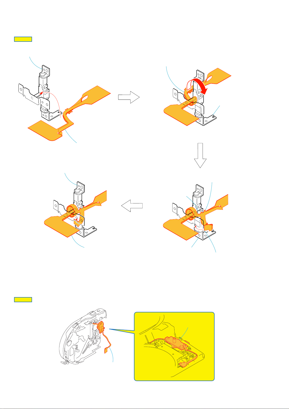
HELP
Sheet attachment positions and procedures of processing the flexible boards/harnesses are shown.
HELP 01
3
1
E
2
Turn over the EVF seiction
1
in the direction of the arrow
2
Two screws (M1.7x5) black
E
Tapping screw
M1.7x5
3-081-204-21
Silver
Black
F
Screw
M1.4x2.5
3-084-681-01
A
A
.
4
B
3
EVF seiction
4
Remove the FP-889 flexible board
in the direction of the arrow
7
D
C
6
B
.
F
5
5
Two screws (M1.7x5) black
6
Remove the VF lens assembly in the direction of the arrow C.
7
Remove the VF cabinet (Upper) in the direction of the arrow D.
HELP
Page 20
DCR-DVD201/DVD201E
HELP 02
2
Hinge (87) assembly
FP-890 board
1
3
Twist the FP-890
flexible board.
Hinge (87) assembly
HELP 03
Hinge (87) assembly
FP-890 board
Adhesive surface
Hinge (87) assembly
5
Attach the adhesive surface.
4
When installing FP-890
flexible board insert it in
the groove.
HELP
Control switch block
(PS8700)
Control switch block
(PS8700)
Page 21

Link
Link
DCR-DVD201/DVD201E
3. BLOCK DIAGRAMS
OVERALL BLOCK DIAGRAM (1/4)
OVERALL BLOCK DIAGRAM (1/4)
OVERALL BLOCK DIAGRAM (2/4)
OVERALL BLOCK DIAGRAM (2/4)
OVERALL BLOCK DIAGRAM (3/4)
OVERALL BLOCK DIAGRAM (3/4)
OVERALL BLOCK DIAGRAM (4/4)
OVERALL BLOCK DIAGRAM (4/4)
POWER BLOCK DIAGRAM (1/3)
POWER BLOCK DIAGRAM (1/3)
POWER BLOCK DIAGRAM (2/3)
POWER BLOCK DIAGRAM (2/3)
POWER BLOCK DIAGRAM (3/3)
POWER BLOCK DIAGRAM (3/3)
Page 22
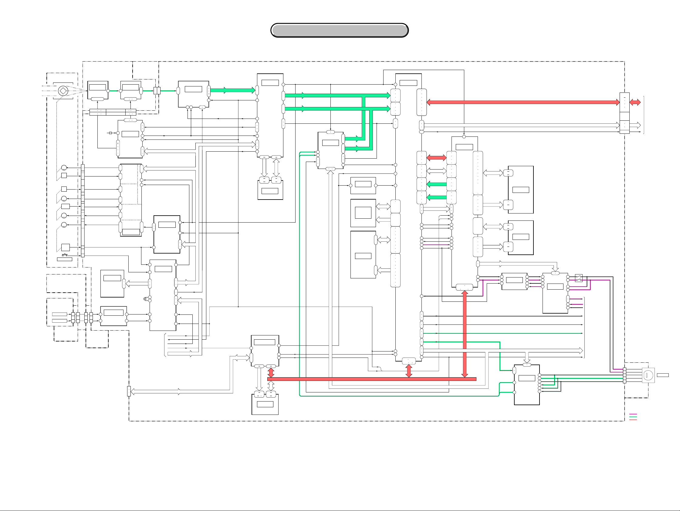
DCR-DVD201/DVD201E
BLOCK DIAGRAMS
3-1. OVERALL BLOCK DIAGRAM (1/4)
LENS ASSY
IRIS
(SHUTTER)
M
H
H
ND FILTER
METER
M
MR
FOCUS
M
MOTOR
M
ZOOM
MOTOR
ZOOM
RESET
SENSOR
NIGHT SHOT
CD-504
BOARD(2/2)
SE-143
BOARD
SE5501
YAW SENSOR
SE5502
PITCH SENSOR
FP-888
FLEXIBLE
CD-504 BOARD(1/2) FP-892
IC5100
11
CCD
IMAGER
1-4 14 • 18
•
V1-V4
RG,H2
CN5101
16-19 29 21
24-21 11 19 32 31 25
CN1601
X1601
66MHz(DVD201)
54MHz(DVD201E)
I DRIVE
23
+,-
22
I HALL
21
+,-
25
ND HALL
17
+,-
15
ND DRIVE
12
+,-
13
2
FMR A,B
1
10
FOCUS +,-
11
ZOOM A,XA
ZOOM B,XB
6
ZOOM +,-
|
9
ZMRST SENS
26
XNS SW
18
CN1501
(11/18)
IC3004
EEPROM
(16/18)
CN5100
352
4
3
2
CN5101
IC1101
12
38
37
YAW/PITCH
SENSOR
8
CN1601CN5206
AMP
FP-892
FLEXIBLE
(2/2)
CN1008
FOR
ADJUSTMENTS
47
72
67
32
17
25
11
H1
J1
C5
B6
C10
B11
K2
L2
B1
C4
F3
E3
K6
L4
G3
F1
IC5101
S/H
IMAGER
13 14 1
8 9 15
38 33 64
(1/18)
IC1601
TIMING
GENERATOR
IRIS DRIVE
ND
FILTER
DRIVE
FOCUS MOTOR
DRIVE
ZOOM MOTOR
DRIVE
IC1501
(3/18)
3
4
2
18
2
13
12
15
16
FLEXIBLE
(1/2)
5
•
4
XSHD,XSHP,CLPDM
J11
K11
H12
K12
H11
K9
L9
M9
J9
SO, SI, SCK
X3002
20MHz
YAW AD
PITCH AD
9
10
12
53
66
5
2
1
1
MS BS
MS DIO
MS SCLK
CCD OUT
EN1
DIR1A
DIR1B
VC-354 BOARD(1/3)
37363
+,-
••
4
CN1601CN5101
HD,VD,FLD HD,VD,FLD
CHCK CHCK
XSYS RST
CAM SO,SI,SCK
(3/18)
17
IC1502
15
16
ZOOM
MOTOR
PRE
DRIVE
18
(11/18)
54
IC3001
187
CAMERA CONTROL
69
70
67
1
3
130
129
TO
OVERALL
BLOCK DIAGRAM
(4/4)
(PAGE 3-8)
XSYS RST
EXT STROBO
ZOOM VR AD
XLK RST
HI SO,SI,SCK
SECTION 3
3. BLOCK DIAGRAMS
3. BLOCK DIAGRAMS
( ) : Number in parenthesis ( ) indicates the division number of schematic diagram where the component is located.
183
77
78
75
73
71
66
65
63
135
30
31
9
•
8
9
5
6
4
XRST
CAM SO,SI,SCK
CH SO,SCK
(1/18)
IC1603
AGC
A/D CONV.
16
20
47
48
AD0-AD13
AD0-AD13
1
12
43 109
44 45
CH SO,SCK
XSYS RST
XLK RST
MS BS
MS DIO
MS SCLK
AD0-AD13
EXT STROBO
56
|
71
CLPOBCLPOB
77
92
91
90
137
22
23
20
102
IC3203(1/2)
140
215
|
213
A1-A22
62 92 60 39
25 163829 36
10
IC1803
161 148
20 26
29
IC1804
(13/18)
DIGITAL
STILL
CONTROL
1 48
(14/18)
IC3401
FLASH MEMORY
32M bit
(2/18)
CAMERA
PROCESS
35
(2/18)
64Mbit
SDRAM
SPCK
115
208
IFI Y0-IFI Y7
|
199
9
IFI C0-C3
|
6
IFI HD
IFI VD
11
IFI OE
12
13
Y OUT
C OUT
XRST VTR
SPCK
SCLK27
S XRST S XRST
C XRST
D0-D15
D0-D15A0-A13
195 174
213
42
45
53
187
128
7
31 68
59
(9/18)
|
IFI Y0-IFI Y7
IC2001
2
6
21
41
76
DO LK-D15 LK DO LK-D15 LK
52
49
VIDEO
|
IFI C0-IFI C7
A/D
42
CONV.
IFI HD
38
IFI VD
IFI OE
37
36
34
64 6366
(4/18)
IC3502
AUDIO
PLL
(5/18)
IC3601
IC3602
128Mbit
SDRAM
(5/18)
IC3603
16Mbit
FCRAM
D0
|
D15
A0
|
A19
IFI Y0-IFI Y7
IFI C0-IFI C7
D0
|
D15
A0
|
A11
SPCK
IFI HD
IFI VD
IFI OE
AFCK
SCLK27
CLK24
107
27
|
42
1
|
20
XSYS RST
B27
AF5 AG3
AD5 AF3
AG4 AD6
AF4 AD7
AG5
AD9
AD8
AC12
AD10
AG8
AG9
AF8
D23
B22
AC13 AC14
AD11-AD18
AF9-AF19
AG10-AG20
AD19-AD21
AD23
AF20-AF23
AG21-AG24
W4 V4
Y1 U4
Y2 W5
W1 T2
W2 T4
V1 U5
V2 R2
U1 V5
T5 U2
R4 T1
R1 R5
P2 P1
N2 P4
N1 N4
M1 M2
L2 L1
K1 M5
K2 M4
B24
B26
AG6
AF6
AG7
AF7
VD SO,SI,SCK
(4/18)
IC3501
DVD
SYSTEM
CONTROL
SDATA0
|
SDATA31
SADRS0
|
SADRS11
SED0
|
SED15
SEA1
|
SEA20
A3-A7
D6-D9
P24
P24
V27
V27
T23
T23
W26
W26
R24
R24
W27
W27
U23
U23
Y26
Y26
HD0-HD15
AA26
AA26
Y27
Y27
AA27
AA27
T24
T24
V23
V23
AB26
AB26
U24
U24
AB27
AB27
V24
HA0-HA2
AD26
W24
XATA REST
AE27
J27
L26
K27
K24
L27
M23
M27
M26
F27
G24
G26
P26
VDIO0-VDIO7
G27
H24
K26
H26
D27
B25
E27
F24
VDIN0-VDIN7
E24
F26
E26
P27
T26
N23
M24
T27
P23
U26
R26
U27
E1
H4
SO 0, SI 0, XSCK 0
G4
HD
N26
ADCK
B23
S VDCK0
H27
C VDCK0
J24
SAD0
B21
BCK
A21
C ADIO
D19
PANEL R
AD1
PANEL G
PANEL B
AC2
AD2
PANEL XHD
J5
PANEL XVD
G2
EVF R
AB1
EVF G
EVF B
AB2
AA2
YOUT
AF2
COUT
AE2
D1
F4
VD SO,SI,SCK VD SO,SI,SCK
E4
XRST VTR XRST VTR
E13
B5-B9
E10 E9
SD0-SD7
VC0-VC7
XSYS RST
C XRST
CN1007
73
75 82
84 86
HD0-HD15
HA0-HA2
XATA REST
B2
90
88
94
92
96
95
97
98
61
2
TO
OVERALL
BLOCK DIAGRAM
(3/4)
(MD-104)
(PAGE 3-5)
(6/18)
IC3701
DVD
CODEC
DATA0 0
DATA0 31
ADRSO 0
ADRSO 10
DATA1 0
DATA1 31
ADRS1 0
ADRS1 10
B23-B26
D21-D27 F24
W4
W1
Y2
Y1
AA1
Y4
AA4
AA2
AB2
AB1
AC2
AC1
|
AD1
AC4
AD4
AD2
AD7
AD5
AE1
AD9
AF1-AF6
AG2-AG4
AG7
AG6
AG5
AD6
AD10
AG8
AC8
AF7
|
AF8
AG9
AG10
AD11
AF9
AF13
AD13-AD21
AF12-AF23
|
AG14-AG23
AG26
AF24
AG24
AD22
AF25
AD23
AG25
|
AB24
AF26
AE26
AF27
AA23
J24
G26
C ADO
A5
C ADIO
D8
BCK
9
8
12
Y OUT
C OUT
C OUT
Y OUT
129
62
90
34
33
37 44
51
129
62
90
34
33
37 44
51
VSP SO X,XVSP SCK X
(15/18)
IC2302
D/A CONV.
A/D CONV.
D0
|
D31
(7/18)
IC3801
64Mbit
SDRAM(0)
A0
|
A10
D0
|
D31
(7/18)
IC3803
64Mbit
SFRAM(1)
A0
|
A10
46
7
34
36
15
16
910
(8/18)
IC2101
VIDEO
IN/OUT
AGC
ACC
L
R
L
3
R
2
15 14
19
17
(15/18)
25
23
IC2301
Y
18
C
14
V
22
Y
39
C
48
V
42
L
54
R
55
L
51
R
53
AUDIO
I/O
SP+
8
SP-
10
MIC L
46
MIC R
49
PANEL R
PANEL G
PANEL B
PANEL XHD
PANEL XVD
TO
OVERALL
3
BLOCK DIAGRAM
(2/4)
(PAGE 3-3)
EVF R
EVF G
EVF B
1
15
CN1006
18
9
11
13
MA-429
6
10
5
9
CN5501
VIDEO/AUDIO
BOARD(1/3)
AUDIO SIGNAL
VIDEO SIGNAL
VIDEO/AUDIO SIGNAL
J2
M2
M1
N4
N1
N2
P2
P4
J4
F1
L4
G1
K2
H1
M4
J1
D1
H4
E1
G2
K4
F2
H2
E2
R2
T1
T2
T4
U1
U4
V1
U2
H24
G27
F26
E4
D4
R5
A4
K1
L2
A2
D7
D0 LK-D15 LK
A23-A26
C27
3-1 3-2
Page 23

DCR-DVD201/DVD201E
3. BLOCK DIAGRAMS
3. BLOCK DIAGRAMS
3-2. OVERALL BLOCK DIAGRAM (2/4)
VC-354 BOARD (2/3)
TO OVERALL
3
BLOCK DIAGRAM (1/4)
(PAGE 3-2)
MA-429 BOARD
(2/3)
MIC901
(MIC UNIT)
MIC
MIC
CN5502
4
L
1
R
J5501
MIC
INT MIC L
INT MIC R
EXT MIC L
EXT MIC R
22
20
26
24
CN1006
(16/18)
35
IC2401
MIC AMP
1
33
3
( ) : Number in parenthesis ( ) indicates the division number of schematic diagram where the component is located.
FP-890
PD-220 BOARD(1/2)
BOARD(1/2)
PANEL R
PANEL G
PANEL B
PANEL XHD
PANEL XVD
SP+
SP-
EVF R
EVF G
EVF B
XRST VTR
MIC L
MIC R
VD SO,SI,SCK
PANEL R,G,B
CN1004 CN001 CN601
6
7
8
PANEL R,G,B
4
20
5
19
6
18
FP-884
FLEXIBLE
(1/2)
HD
17
VD
18
25
22
24
27
26
HD
VD
VD SO,SCK
9
8
1
4
2
CN5303 CN5302
7
8
15
16
22
19
21
34
33
IC602
32
DRIVE
45
42
44
TIMING
GENERATOR
48
1
1
2
SP901
(SPEAKER)
RGB
20
21
22
24
26
17
5
18
31
VR,VG,VB
VP
BL ON
EXT DA
JS-030
MIC L
22
14
36
48
MIC R
SHOE MIC L
BOARD(1/2)
8
CN1002
FP-883
FLEXIBLE
INTELLIGENT
ACCESSORY
SHOE (1/2)
(1/2)
LB-107 BOARD
6
7
8
4
5
9
18
2
CN301
R,G,B
COM
PSIG
EN,VST,REF,PCG,VCK,STB,BLK,HCK2,HCK1
EVF R,G,B
VD SO,SCK
VD SO,SCK
HD
VD
XRST VTR
8
(10/18)
IC2202
Q2203
BACK
LIGHT
DRIVE
CN2201
15
14
13
17
16
12
3
19
(10/18)
34
33
IC2201
32
RGB
DRIVE
45
42
44
48
TIMING
GENERATOR
1
3
20
21
22
26
24
28
17
6
BL ON
18
EXT DA
31
IC601
Q604_607
BACK
LIGHT
DRIVE
BL -15.5V
CN302
D303
BACK
LIGHT
BL H
CN605
PSIG
COM
CN606
LCD901
4
5
COLOR LCD
3
UNIT
6
24
23
22
|
19
14
|
11
9
|
7
2
1
3
LED901
BACK
LIGHT
AUDIO SIGNAL
VIDEO SIGNAL
LCD902
17
COLOR
EVF
18
UNIT
16
21
19
20
15
9
7
5
FP-889
FLEXIBLE
3-3 3-4
Page 24

3. BLOCK DIAGRAMS
3. BLOCK DIAGRAMS
DCR-DVD201/DVD201E
3-3. OVERALL BLOCK DIAGRAM (3/4)
MD-104 BOARD (1/2) BASE UNIT
CN4901
73
82
75
86
84
HD0-HD15
88
TO
OVER ALL
2
BLOCK DIAGRAM
(1/4)
(VC-354)
(PAGE 3-2)
J902
USB
FP-887 FLEXIBLE
TO
OVER ALL
5
BLOCK DIAGRAM
(4/4)
(VC-354)
(PAGE 3-8)
FP-891
FLEXIBLE
M
M901
EJECT
MOTOR
S892
OPEN
S891
(LID OPEN)
S893
(EJECT DET)
D891
(ACCESS)
90
94
92
96
95
98
97
61
CN4201
7
6
CN4901
70
72
66
68
64
67
29
CN4907
3
9
10
7
1
5
HA0-HA2
XATA RESET
XRST BRIDGE
IC4701 RESET
SO,SI,SCK
EJECT SW
LID OPEN
Q4903
LED
DRIVE
Q4906,4907,4909
MOTOR
DRIVE
D4202
USB D+,D-
(4/8)
IC4707
1
4
2
LID OPEN R
EJECT DET
ACCESS LED
PLG
EJECT STOP
22
39
76
103
105
4
82
114
133
132
134
16
24
123
125
122
92
( ) : Number in parenthesis ( ) indicates the division number of schematic diagram where the component is located.
Since a service is provided only for the MD BLOCK ASSY (A-7113-371-A) and not for the single MD-104 board, complete.
HD0-HD15
85
67
(2/8)
IC4601
DVD
DSP
56 62
89 91
84 749
14 21
(5/8)
IC4201
USB 2.0
BRIDGE
(4/8)
HA0-HA2
3
X4201
30MHz
46
73
SDA,SCL
36
27
MD0-MD7,AD0-AD19
47
MA MA
55 57
5
6
(5/8)
IC4200
EEPROM
(2/8)
IC4607
64Mbit
SDRAN
213
42 53
20 26
29 35
SBD0-SBD15
SBA0-SBA13
X4601
22.5792MHz
MD0-MD7
98
96
99
126
110
148
133
208
209
49
56
IC4701
DVD
DRIVE
CONTROL
MD0-MD7,AD8-AD15
AD16-AD19
34
(4/8)
D/A CONV.
78
13 14
17 18
11
1
2
3
MD0-MD7,AD8-AD15
DSP RSTX DSP RSTX
72 65
LD ON
119
ACT EN
88
IN LIMIT X
6
FOO
17
TRO
19
110
X4701
8MHz
112
VRD
20
S VRD
21
DMO
22
S DMO
23
FG
128
SLED EN
101
SKEW1
103
SKEW2
104
SPDL EN
89
SKEW EN
102
DADATA
DACK
138
DALD
140
97
XSHK T M
107
XSHK F M
83
6
7
8
IC4706
(4/8)
IC4703
IC4704
ADDRESS
LATCH
S VRD
S DMO
SNS F COMP2
SNS F COMP
25
69
12 15
16 19
LA1-LA15
IC4801
IC4804
FOCUS SHOCK DETECTOR
29 36
39 46
16 23
25 26
48
FLGA
(6/8)
-
IC4807
18
D0
D15
A0
A18
(4/8)
IC4702
FLASH
MEMORY
SVRD
IC4852
VRD
5
3
TEST FEO
FLGA
(3/8)
20
(3/3)
IDLE
XSHK T M
XSHK F M
165
VRD
(3/8)
IC4855
4
BUFFER
9
7
(6/8)
IC4803
MMV
CN4902
FOR
ADJUSTMENTS
17 12 14 18
CN4501
LD ON
6
FDPD IC OUT
11
12
5
6
48
VO4+,VO4-
47
VO3+,VO344
43
34
41
29
24
1
2
15
16
SE4802
SHOCK
SENSOR
EFM PK
EFM WP
RF +
RF -
FCS+
FCS-
TRK+
TRK-
CN4851
CN4852
IN LIMIT X
H1+,H1H2+,H2H3+,H3-
CN4801
VO3 (+)
VO3 (-)
VO4 (+)
VO4 (-)
7
16
35
34
23
A-K
30
40
1
4
3
2
4
6
5
3
1
A1
A2
9
A3
8
7
10
11
14
17
13
12
9
8
15
14
11
10
42
41
169
170
185
186
3
17
18
19
187
173
FOO
192
TRO
193
FMO
196
FMOS
197
DMO
198
FG
205
41
11
5
S VRD
S DMO
VRD2
RFOP
RFON
FEO
TEO
VRCK
SCL
SCB
SCD
LVL
WOB
IC4852
FOO
12
S VRD
13
FMO
2
FMOS
12
VRD2
1
13
IC4854
IC4852
DMO
2
S DMO
1
35
34
25
29
21
19
18
17
24
7
(3/8)
(1/8)
IC4502
RF
PROCESS
44
72
71
61
69
55
(1/3)
FOCUS
DRIVE
TRACKING
DRIVE
(3/8)
IC4853(1/2)
SLED
MOTOR
DRIVE
(3/8)
IC4853(2/2)
SPINDLE
MOTOR
DRIVE
SKEW
MOTOR
DRIVE
(6/8)
SHOCK
SENSOR
AMP
1
2
15
16
(3/8)
(3/8)
IDLE
IDLE
IDLE
14
ACTEN
VRD2
15
FMOS O
14
(2/3)
DMO O
15
SPDL EN
SKEW1
SKEW2
SKEW EN
7
FOO
TRO
FMO O
FG
57
56
17
49
60
61
62
31
64
58
59
19
IC4808
LD
DRIVE
PD IC
FPD IC
FOCUS
COIL
TRACKING
COIL
M
IN LIMIT
PD
M
H
M
SLED MOTOR
SPINDLE MOTOR
SKEW MOTOR
LASER
DIODE
VIDEO/AUDIO SIGNAL
3-5 3-6
Page 25

DCR-DVD201/DVD201E
3. BLOCK DIAGRAMS
3. BLOCK DIAGRAMS
3-4. OVERALL BLOCK DIAGRAM (4/4)
1
4
PD-220
BOARD
(2/2)
Q4001,
4002
JS-030 BOARD (2/2)CONTROL SWITCH
S5301, 5303, 5304
JOY STICK,
VISUAL INDEX, BACK LIGHT
DISPLAY BATT INFO
CN601
2
9
Q4005,
4006
S5302
FP-890
BOARD (2/2)
K2
D2
D1
CONTROL SWITCH
BLOCK (BL8700)
BT901
BATTERY
TERMINAL
J901
DC IN
BLOCK (SH8700)
S108-114
STOP, PAUSE, PLAY,
NEXT, EDIT, FINALIZE
S100-107
REC, SETUP, EXPOSURE,
FOCUS, FADER, VOL+, VOL-
S002
LCD
BACK LIGHT
S001
REC
START/STOP
MD-104 BOARD (2/2)
Since a service is provided only for the MD BLOCK ASSY (A-7113-371-A)
and not for the single MD-104 board, complete.
CN4002
1
S
2
3
1
2
3
CN4001
CN602
6
1
VTR DD ON
SHOE ON
BATT/XEXT SW
FAST CHARGE
BATT SIG
( ) : Number in parenthesis ( ) indicates the division number of schematic diagram where the component is located.
FP-884
FLEXIBLE
CN5303CN5301
S001
PANEL
REVERSE
LANC SIG
FAST CHARGE
3V REGC1 C2
(8/8)
(2/2)
2
4
3
S002
5
PANEL
OPEN/
CLOSE
(SECONDARY)
S001
RESET
CN001
15
RESET
IC4001
DC/DC
CONVERTER,
RESET,
LANC I/O
BT5201
LITHIUM
BATTERY
L3
K3
A3
D3
E2
E3
G1
LANC OUT
LANC IN
XRESET
VOUT
CAM DD ON
VC-354 BOARD (3/3)
CN1004
32
30
31
5
4
3
11
CN1007
4741 4313
4741 4313
CN4901
EVER 3.0V
A 1.2V
D 1.2V
A 1.5V
D 1.5V
D 2.5V
WG1 A 2.5V
WG1 D 2.5V
A 2.8V
D 2.8V
AU 2.8V
EP 2.8V
D 3.1V
A 4.6V
AU 4.6V
EP 4.6V
DRV A 4.6V
DRV MT 4.6V
MT 4.6V
EP 8.5V
CAM 15V
CAM -7.5V
A 2.5V
BATT UNREG
VTR UNREG
SHOE UNREG
CN4901
VTR DD ON
FAST CHARGE
SHOE ON
BATT/XEXT SW
BATT SIG
61 KEY AD2
(12/18)
66 KEY AD4
65 KEY AD3
20
21
3 XBATT VIEW29
73 HI XRESET
69 KEY AD7
CN1007
55
55
53
53
71
71
35
35
31
31
10
10
25
25
27
27
18
18
57
57
40
39
14
53
62
35 VTR DO ON
37 FAST CHARGE
75 SHOE ON
74 BATT/XEXT SW
HI EVER SO
HI EVER SCK
LANC OUT
LANC IN
VCC
IC3103
HI CONTROL
F TALLY LED
4XEJECT SW
TXD
23
RXD TXD, RXD, SCK
24
SCK
25
52
X 0A
SIRCS SIG
IB SO
IB SI
SHOE ID2
SHOE ID1
32.768KHz
51X 1A
29X TAL
10MHz
28X TAL
47XSYS RST
44XLK RST
7XPOWER ON
1MODE 0
2MODE 1
59KEY AD0
6XPHOTO FREEZE
60KEY AD1
67KEY AD5
9POWER LED
12CHARGE LED ON
15IR ON
41
10
42
43
58
57
X3102
X3101
Q3103
LED
DRIVE
Q1001
LED
DRIVE
I/F
Q3102
IC3203 (2/2)
TXD
190
RXD
191
SCK
185
140
XLK RST
168
CAM DD ON
(13/18)
HI CONTROL
SHOE UNREG
EEP TXD
EEP RXD
EEP SCK
HI SO
HI SI
H1 EVER SCK
CN1001
CN1006
CN1002
8
6
5
4
3
16
15
13
2
12
11
19
6
2
4
6
5
4
3
2
1
16
202
203
204
207
206
205
200
201
HI, SO, SI, SCK
199
ZOOM VR AD
EXT STROBO
EXT STROBO
SHOE ID 1, 2
LANC SIG
SHOE UNREG
FP883
FLEXIBLE
(2/2)
XSYS RST
XLK RST
(LID OPEN)
IC4701 RESET
XRST BRIDGE
(POWER)
(CHARGE)
EJECT SW
67
72
70
66
68
SO, SI, SCK
69
LID OPEN
29
CN1007
IC3302
TO
1
OVERALL
BLOCK DIAGRAM(1/4)
(13/18)
EEPROM
5
2
6
(PAGE 3-1)
CONTROL SWITCH
D5503
D5502
(TALLY)
BLOCK (PS8700)
START/STOP SW
SUPER NS PLUS/
D 2.8V
PHOTO FREEZE
PHOTO REC
ZOOM AD
(INFRARED RAY EMITTER)
MA-429 BOARD (3/3)
INTELLIGENT
ACCESSORY
SHOE
(2/2)
5
POWER SW
MODE SW
PHOTO SW
ZOOM SW
COLOR SLOW S
IC5501
REMOTE
4
COMMANDER
RECEIVER
TO
OVERALL
BLOCK DIAGRAM
(3/4)
(MD-104)
(PAGE 3-5)
REMOTE
3-7 3-8
Page 26

3. BLOCK DIAGRAMS
3. BLOCK DIAGRAMS
DCR-DVD201/DVD201E
3-5. POWER BLOCK DIAGRAM (1/3)
MD-104 BOARD (1/2)
Since a service is provided only for the MD
BLOCK ASSY (A-7113-371-A) and not for the
single MD-104 board, complete.
CN4002
BATT UNREG
1
2
3
1
2
3
BATT SIG
CN4001
ACV UNREG
BATT/XEXT
4
3
14
5
4
6
10
9
7
17
CN1004
CN1001
D 2.8V
R1002
R1001
LF4001
Q4001,
4002
26 28
26
CHARGE
SWITCH
FAST CHARGE
31 3325 27
31 3325 27
VC-354 BOARD (1/2)
Q3102
I/F
BATT SIG
CN1007
28
CN4901
REMOTE
BT901
BATTERY
TERMINAL
S
J901
DC IN
FP-884
FLEXIBLE
CONTROL
SWITCH
BLOCK
(PS8700)
MODE
BT5201
LITHIUM
BATTERY
(SECONDALY)
POWER
LID OPEN SW
(1/2)
S001
RESET
ZOOM VR
CHARGE LED
POWER LED
( ) : Number in parenthesis ( ) indicates the division number of schematic diagram where the component is located.
D4004
EVER 3.0V
D4001
VOUT
HI XRESET
5
16
CAM 15V
CN4902
FOR
ADJUSTMENTS
C1
C2
B2
D2
D3
A3
A2
E2
E3
E4
D1
L2
H1
J2
J11
K1
DIN
CLK
LD
CTL1
LANC I/O
V VTR
LANC DC
3V REG
RESET
(8/8)
IC4001
DC/DC CONVERTER
RESET,LANC I/O
BATTERY
IN
DETECT
5.6V
REG
13.5V
REG
15V
REG
CAM DD ON
PVCC1
VBATP
PVCCH
SSO 1V
PVCCL2
SWV09
DRV9
SSDO
CDET
SHOE UNREG
(8/8)
IC4002
(1/2)
Q4007
Q4015
SWITCHING
SWITCHING
A9
HO1
A10
LO1
B8
VO1
B11
HO2
C10
LO2
A8
VO2
C9
HO3
D10
LO3
D7
VO3
E10
HO5
E8
LO5
A5
VO5
A4
C8
D9
HO4
E11
LO4
D5
VO4
K10
F11
E1
F10
HO6
F8
LO6
K4
VO6
K11
J11
H9
H8
VO9
G2
H2
G1
Q4008
SWITCHING
Q4009
SWITCHING
Q4011
SWITCHING
Q4010
SWITCHING
Q4012
SWITCHING
L4001
Q4014
SWITCHING
Q4016
SWITCHING
Q4017
SWITCHING
Q4019
SWITCHING
Q4018
SWITCHING
Q4023
SWITCHING
Q4020
SWITCHING
L4007
L4002
L4003
L4004
L4006
L4008
L4005
C4063
C4052
1.5V
1.2V
2.5V
4.6V
2.8V
D4008
RECT
PVCCH
5V
D4007
RECT
15V
Q4003,
4004
BATT LI 3V
HI XRESET
54
55
75
74
38
37
42
43
56
1
2
7
INIT CHARGE ON
BATT SENS
ACV SENS
SHOE ON
BATT/XEXT
INIT CHARGE ON
FAST CHARGE
IB SO
IB SI
VTR DD SENS
MODE 0
MODE 1
XPOWER ON
IC3103
F4003
BATT
VTR UNREG
HI CONTROL
F4005
F4002
F4004
F4001
UNREG
XLANC PWR ON
SHOE ON
XRESET
BATT IN
HI EVER SO
HI EVER SCK
XCS DD
VTR DD ON
(12/18)
Q4005, 4006
10
10
14
VCC
53
62
73
31
20
21
49
35
BATT UNREG
MT UNREG
CN4901
CN1007
8
CN1007
VTR UNREG2
VTR UNREG
23
74
13
71
47
45
41
43
39
35
51
JIG UNREG
23
2121
74
13
71
47
45
41
43
39
35
51
5959
CN4901
(8/8)
IC4003
8.5V
REG
4
SS0
SS0
Q4024
3.1V REG
7
VCC
5 6
L4016
L4013
L4017
L4014
L4027
L4023
L4019
L4015
L4010
L4028
L4026
L4024
L4021
Q4022
2.5V REG
1
3
L4018
L4011
8
A 1.5V
D 1.5V
A 1.2V
D 1.2V
D 2.5V
EP 4.6V
A 4.6V
AU 4.6V
DRV A 4.6V
A 2.8V
AU 2.8V
D 2.8V
EP 2.8V
2
MT 4.6V
DRV MT 4.6V
BL -15.5V
D 3.1V
EP 8.5V
L4025
L4022
L4020
IC4002
(2/2)
CN4901
A 2.5V
WG1 D 2.5V
WG1 A 2.5V
(8/8)
12 14
30 32
50 52
20 22
26 28
17 19
44 46
SHOE UNREG
9 11
EP 4.6V
40
EP 8.5V
15
EP 2.8V
38
BL -15.5V
16
CAM DD ON
18
A 1.2V
34
D 1.2V
1
TO
POWER
BLOCK
AU 4.6V
42
AU 2.8V
36
A 2.8V
A 1.5V
48
D 1.5V
54
D 3.1V
24
D 2.5V
D 2.8V
MT 4.6V
A 4.6V
CAM 15V
56
CAM -7.5V
58
DRV MT 4.6V
DRV A 4.6V
WG1 D 2.5V
WG1 A 2.5V
A 2.5V
D 2.5V
A 2.8V
D 1.5V
D 2.8V
D 3.1V
DIAGRAM(2/3)
(VC-354)
(PAGE 3-11)
2
TO
POWER
BLOCK
DIAGRAM(3/3)
(PAGE 3-13)
(8/8)
-15V
2
SSDO (1V)
IC4004
-7.5V
REG
3
CAM -7.5V
1
5
CAM DD ON
FP-891
FLEXIBLE
ACCESS LED
9
CN4907
R4945
D 2.8V
Q4906,4907,4909
EJECT
MOTOR
DRIVE
DRV MT 4.6V
DRV MT 4.6V
D 2.8V
EP 2.8V
EP 8.5V
CAM 15V
3-9 3-10
Page 27

DCR-DVD201/DVD201E
3. BLOCK DIAGRAMS
3. BLOCK DIAGRAMS
3-6. POWER BLOCK DIAGRAM (2/3)
FP-883
FLEXIBLE
SHOE UNREG
CN1002CN1007
1 2
1
TO
POWER BLOCK
DIAGRAM
(1/3)(MD-104)
(PAGE 3-10)
SHOE UNREG
EP 4.6V
EP 8.5V
EP 2.8V
BL -15.5V
CAN DD ON
A 1.2V
D 1.2V
AU 4.6V
AU 2.8V
A 2.8V
A 1.5V
D 1.5V
D 3.1V
D 2.5V
D 2.8V
MT 4.6V
A 4.6V
9 11
40
15
38
16
18
34
12 14
42
36
30 32
48
50 52
54
24
20 22
26 28
17 19
44 46
( ) : Number in parenthesis ( ) indicates the division number of schematic diagram where the component is located.
INTELLIGENT
ACCESSORY
SHOE
Q2307
MT 4.6V
AU 4.6V
AU 2.8V
D 2.8V
D 1.5V
A 2.8V
A 1.5V
D 1.5V
D 3.1V
D 2.5V
D 2.8V
MT 4.6V
SP VCC
REGREG
L1101
(7/18)
IC3801
IC3803
64Mbit
SDRAM
(15/18)
IC2301
AUDIO
I/O
SE 2.8V
EP 2.8V
EP 8.5V
EP 4.6V
L2202
(4/18)
IC3501
DVD
SYSTEM
CONTROL
L2203
(15/18)
IC2302
AUDIO
D/A CONV.
A/D CONV.
(10/18)
IC2201
RGB
DRIVE
TIMING
GENERATOR
(6/18)
IC3701
DVD
CODEC
BL ON
18
EXTDA
31
(16/18)
IC2401
MIC
AMP
IC2202
Q2203
BACK
LIGHT
DRIVE
IC3601
IC3602
(5/18)
128Mbit
SDRAM
19
20
(11/18)
IC3004
EEPROM
FP-889
FLEXIBLE
1
IC3603
(5/18)
16Mbit
FCRAM
LB-107 BOARD
CN301CN2201
20
LED K
2
1
(11/18)
IC3001
CAMERA
CONTROL
(BACK LIGHT)
ZS RST LED
55
(4/18)
IC3502
AUDIO
PLL
EP 8.5V
14
CN302
VDD
LCD902
COLOR
2
EVF
UNIT
EP 2.8V
EP 4.6V
12
13
FP-884
FLEXIBLE
(2/2)
D303
BL -15.5V
15
NS 2.8V
D 2.8V
CAM DD ON
16
28
D 1.5V
A 1.5V
168
IC3203
AU 2.8V
A 4.6V
L001
CN001CN1004
12
14
13
11
10
(13/18) (13/18)
IC3302
CONTROL
DIGITAL
CONTROL
D2.8V
D 3.1V
HI
STILL
EEPROM
FB3202
A 1.2V
D 1.2V
FP-890
BOARD
JS-030 BOARD
CN5303
6
(2/18)
IC1803
CAMERA
PROCESS
D 2.8V
MT 4.6V
SE 2.8V
PD-220 BOARD
CN601
12
10
11
L602
13
14
CN5301
2
3
(2/18)
IC1804
R1007,1008
IC602
(14/18)
IC3401
64Mbit
SDRAM
RGB
DRIVE
TIMING
GENERATOR
FUNCTION
SWITCH
32Mbit
FLASH
MEMORY
Q608,609
XSTBY
10
BL ON
18
EXT DA
31
CONTROL
SWITCH
BLOCK
(SH8700)
NS LED A
CN1006
IC601
BACK LIGHT
DRIVE
5
3
7
1
Q604-607
D5502
TALLY LED
D5503
INFRAED REY
EMITTER
LED
DRIVE
LCD901
2.5 INCH
CN605
COLOR
VDD
BACK
BL H
LIGHT
BL L
CN606
LCD
18
UNIT
LED901
BACK
LIGHT
1
3
6
IC5501
REMOTE
COMMANDER
RECEIVER
CAM 15V
CAM -7.5V
CN1008
FOR
ADJUSTMENTS
56
58
D 2.8V
17
D 3.1V
3
VC-354 BOARD
(2/2)
(3/18)
IC1503
2.8V
REG
4
MA-429 BOARD
CD-504BOARD
CN5101 CN5100 CN5206
IC5100
CCD
IMAGER
IC5101
S/H
1 6
SE-143 BOARD
ZOOM
RESET
SENSOR
FOCUS
MR
SENSOR
LENS ASSY
FP-888
FLEXIBLE
SE5501,5502
YAW
PITCH
SENSOR
A 2.8V
IMG VH
IMG VL
60
Z M VCC
MR A 2.8V
(1/18)
IC1601
TIMING
GENERATOR
35
8 32
CAM 15V
9 31
CAM -7.5V
10
28
CN1601
29
3
CN1501
FP-892
FLEXIBLE
5
30
12
A 2.8V
D 2.8V
A 4.6V
51
(16/18)
IC1101
PITCH/
YAW
SENSOR
AMP
MR A 2.8V
(9/18) (8/18) (3/18) (3/18)
IC2001
VIDEO
A/D CONV.
IC2101
VIDEO
IN/OUT
AGC
ACC
L1502
IC1501
FOCUS/Z OOM/
IRIS/ND
DRIVE
IC1502
ZOOM
MOTOR
PRE DRIVE
(1/18)
IC1603
AGC
A/D CONV.
ZS RST LED
D 2.8V
CAM DD ON
A 4.6V
IC1604
5 4
Q1501
(1/18)
3.1V REG
5
(1/18)
IC1602
3.4V REG
3.4V
4
3.1V
3-11 3-12
Page 28

3. BLOCK DIAGRAMS
3. BLOCK DIAGRAMS
DCR-DVD201/DVD201E
3-7. POWER BLOCK DIAGRAM (3/3)
MD-104 BOARD (2/2)
Since a service is provided only for the MD
BLOCK ASSY (A-7113-371-A) and not for the
single MD-104 board, complete.
TO
POWER BLOCK
2
DIAGRAM
(1/3)
(PAGE 3-10)
D 2.8V
A 2.5V
D 2.5V
D 3.1V
D 1.5V
WG1 A 2.5V
WG1 D 2.5V
A 2.8V
DRV A 4.6V
DRV MT 4.6V
D 2.8V
A 2.8V
DRV A 4.6V
DRV MT 4.6V
(5/8)
IC4201
USB 2.0
BRIDGE
IC4200
EEPROM
L4200
(5/8)
( ) : Number in parenthesis ( ) indicates the division number of schematic diagram where the component is located.
(4/8)
(2/8)
IC4601
DVD
DSP
(4/8)
IC4703
IC4704
ADDRESS
LATCH
FB4603
FB4701
(2/8)
IC4603
IC4606
PERIPHERAL IC
(4/8)
IC4702
FLASH
MEMORY
(2/8)
IC4607
64Mbit
SDRAM
(4/8)
IC4707
AND
GATE
IC4502
(1/8)
DVD
PROCESS
IC4701
RF
(4/8)
DVD
DRIVE
CONTOROL
A 2.8V
121
INSW X
84
(1/8)
IC4503
GATE
IC4706
D/A CONV.
Q4701
BUFFER
OP PWR X
INSW X
(6/8)
IC4808
AND
D 2.8V
A 2.8V
DRV A 4.6V
DRV MT 4.6V
SHOCK
SENSOR
AMP
Q4852
R4895
LDD VCC
PD VCC
FPDIC VCC
Q4501
IN SW
A 2.8V
DRV A 4.6V
CN4501
CN4852
R4949
BASE UNIT
8
9
31
39
2
6
12
LD DRIVE
PD IC
FPD IC
IN LIMIT
PD
SPINDLE
MOTOR
(3/8)
IC4853
FOCUS DRIVE
TRACKING DRIVE
SLED MOTOR DRIVE
SPINDLE MOTOR DRIVE
SKEW MOTOR DRIVE
(3/8)
IC4852
IC4854
SELECTOR
(3/8)
IC4855
VRD2
BUFFER
(6/8)
IC4803
MMV
(6/8)
IC4801
OR GATE
(6/8)
IC4804
IC4807
FOCUS
SHOCK
DETECTOR
3-13 3-14E
Page 29

SECTION 4
PRINTED WIRING BOARDS AND SCHEMATIC DIAGRAMS
4-1. FRAME SCHEMATIC DIAGRAM (1/3)
4-2. SCHEMATIC DIAGRAMS 4-3. PRINTED WIRING BOARDS
4-2. SCHEMATIC DIAGRAMS 4-3. PRINTED WIRING BOARDS
DCR-DVD201/DVD201E
1
A
B
3
SE-143
BOARD
CN5206
6P
1
PS_V
PS_LI F_TALLY_LED
YS_V
YS_LI
SE_GND
A_2.8V
1
2
3
4
5
FP-888
FLEXIBLE
6
A_2.8V
SE_GND
YS_LI
YS_V
PS_LI
PS_V
2
3
4
5
6
CD-504
BOARD
C
D
LENS
E
5
CN5101
39P
6PCN5100
CAM_-7.5V
CCD_OUT-
CCD_OUT+
YS_LI
PS_LI
SE_2.8V
SE_GND
SE_GND
XSHD
XSHP
A_2.8V
VSUB
RCSUB
CLPDM
CAM_15V
CAM_15V
PS_V
YS_V
GND
GND
GND
GND
GND
GND
GND
GND
GND
GND
GND
1
2
3
4
5
6
7
8
9
10
11
12
13
14
15
V1
16
V4
17
V2
18
V3
19
20
H2
21
H1
22
H4
23
H3
24
LH
25
26
27
28
RG
29
30
31
32
33
34
35
36
37
38
39
CN1601
39
38
37
36
35
34
33
32
31
30
29
28
27
26
25
24
23
22
21
20
19
18
17
16
FP-892 FLEXIBLE
15
14
13
12
11
10
9
8
7
6
5
4
3
2
1
39P
PS_V
YS_LI
PS_LI
YS_V
SE_2.8V
SE_GND
SE_GND
XSHD
XSHP
GND
GND
A_2.8V
VSUB
RCSUB
CLPDM
V1
V4
V2
V3
GND
H2
H1
H4
H3
LH
GND
GND
GND
RG
CAM_-7.5V
CAM_15V
CAM_15V
GND
GND
GND
CCD_OUT-
CCD_OUT+
GND
GND
911126842
107
27P
CN1006
AV_MULTI_DET
SIRCS_SIG
A_4.6V INT_MIC_R
AU_2.8V
NS_LED_K
NS_LED_A
REG_GND
S_Y_I/O
REG_GND
S_C_I/O
REG_GND
VIDEO_I/O
REG_GND
AUDIO_L_I/O
REG_GND
MIC_GND
AUDIO_R_I/O
MIC_GND
INT_MIC_R
MIC_GND
INT_MIC_L
MIC_GND
EXT_MIC_R
MIC_GND
EXT_MIC_L
MIC_GND
1
2
3
4
5
6
7
8
9
10
11
12
13
14
15
16
17
18
19
20
21
22
23
24
25
26
27
MA-429
BOARD
6PCN5502
MIC_GND
MIC_GND
INT_MIC_L
MIC_GND
MIC_GND
13
MIC901
MIC UNIT
1
R
2
3
4
L
5
6
F
123456789
F_MR_B
G
H
SHOE_UNREG
SHOE_UNREG
LANC_SIG
INTELIGENT
ACCESSORY
SHOE
I
16
SHOE_ID1
SHOE_ID2
EXT_STROBO
SHOE_MIC_GND
SHOE_MIC_L
SHOE_GND
SHOE_GND
FP-883
FLEXIBLE
1
2
3
4
5
6
7
8
9
10
F_MR_A
29P
CN1501
CN1002
10P
SHOE_UNREG
SHOE_UNREG
LANC_SIG
SHOE_ID1
SHOE_ID2
EXT_STROBO
SHOE_MIC_GND
SHOE_MIC_L
SHOE_UNREG_GND
SHOE_UNREG_GND
F_MR_VCC
MR/TEMP_GND
ZOOM_A
LENS_TEMP_OUT
4-1 4-2
10111213141516171819202122232425262728
ZOOM_XB
ZOOM_XA
ZOOM_B
FOCUS+
FOCUS-
N_DRIVE-
N_DRIVE+
ND_BIAS-
ND_HALL-
ND_BIAS+
ND_HALL+
IR_SW_OUT
I_BIAS+
IR_SW_GND
I_HALL+
I_DRIVE-
I_BIAS-
I_DRIVE+
I_HALL-
ZM_OUT
ZM_GND
MAKER_SELECT
29
ZM_VCC
VC-354 BOARD(1/3)
TO
VC-354 BOARD
(2/3)
FRAME SCHEMATIC DIAGRAM (1/3)
Page 30

DCR-DVD201/DVD201E
FRAME SCHEMATIC DIAGRAM (2/3)
4-2. SCHEMATIC DIAGRAMS 4-3. PRINTED WIRING BOARDS
4-2. SCHEMATIC DIAGRAMS 4-3. PRINTED WIRING BOARDS
1
3
A
LB-107 BOARD
B
C
20P
EVF_HCK2
LED_K
EVF_VR
EVF_PSIG
EVF_BL_GND
EP_4.6V
EVF_COM_CS
CN301
123456789
EVF_EN
EVF_VST
EVF_VG
EVF_VB
1011121314151617181920
EVF_REF
EVF_PCG
EVF_VCK
EVF_STB
EVF_BLK
EVF_HCK1
EVF_HST
REG_GND
EVF_VDD
CN302
5
21P
COM
21
PSIG
20
CS
19
VG
18
VR
17
VB
16
PCG
15
EN
14
VCK
13
VST
12
STB
11
REF
10
BLK
9
RGT
8
HCK1
7
HCK2
6
HST
5
VSSG
4
VSS
3
2
VDD
1
N.C.
684 17 182
LCD902
COLOR
EVF UNIT
7
CONTROL SWITCH BLOCK
(PS8700)
D
FP-889 FLEXIBLE
EVF_HCK1
EVF_HCK2
EVF_HST
REG_GND
123456789
EVF_VDD
1011121314151617181920
LED_K
EP_4.6V
E
20P
CN2201
EVF_COM_CS
EVF_BL_GND
EVF_PSIG
EVF_VR
EVF_VG
EVF_VB
EVF_EN
EVF_VST
EVF_REF
EVF_PCG
EVF_VCK
EVF_STB
EVF_BLK
123456789
MODE1
MODE0
KEY_AD5
XS/S_SW
REG_GND
20P
CN1001
XPOWER_ON
1011121314151617181920
D_2.8V
RID_OPEN
VTR_UNREG
POWER_VCC
CHARGE_LED_ON
F
91411 12 16
13
1510
2PCN5302
JB-030 BOARD
33PCN1004
REG_GND
33
KEY_AD2
ZOOM_AD
POWER_LED
D_2.8V
KEY_AD1
XPHOTO_FREEZE
LANC_DC
XLANC_JACK_IN
LANC_SIG
REG_GND
KEY_AD3
KEY_AD4
XBATT_VIEW
D_2.8V
VD_SO
VD_SCK
XCS_LCD
REG_GND
BL_GND
BL_GND
PANEL_VD
PANEL_HD
NS_2.8V
BL_-15.5V
EP_8.5V
EP_4.6V
EP_2.8V
KEY_AD7
REG_GND
REG_GND
PANEL_B
PANEL_G
PANEL_R
KEY_AD6
BATT_LI_3V
HI_XRESET
REG_GND
REG_GND
VD_SI
32
31
30
29
28
SP+
27
SP-
26
25
24
23
22
21
20
19
18
17
16
15
14
13
12
11
10
9
8
7
6
5
4
3
2
1
20P
CN001
8P
REG_GND
KEY_AD2
KEY_AD3
CN5303
1234567
FP-884 FLEXIBLE
BL_GND
VD_SCK
XCS_LCD
SE_GND(REG_GND)
PANEL_VD
VD_SI
BL_GND
VD_SO
123456789
FP-890 BOARD
SP+
D_2.8V
SP-
KEY_AD4
XBATT_VIEW
8
KEY_AD7
BL_-15.5V
PANEL_HD
NS_2.8V
EP_8.5V
1011121314151617181920
EP_4.6V
EP_2.8V
REG_GND
REG_GND
PANEL_B
PANEL_G
6PCN5301
PANEL_R
KEY_AD2
D_2.8V
D_2.8V
KEY_AD3
REG_GND
REG_GND
SP(+)
SP(-)
BT5201
LITHIUM BATTERY
(SECONDARY)
1
2
1
2
3
4
5
6
CONTROL SWITCH
BLOCK
(SH8700)
SP901
SPEAKER
PANEL_G
PANEL_R
N.C.
PANEL_RVS_SW
123456789
REG_GND
CN602
CN606
CN605
24P
6P
BL_2.8V
6P
REG_GND
REG_GND
BL_ON/OFF_SW
N.C.
VSSG
XSTBY
TEST1
WIDE
HCK2
HCK1
PSIG
TEST2
BL_FB
BL_L
BL_H
2nd S/S
24
COM
23
CS
22
VST
21
VCK
20
EN
19
DWN
18
VDD
17
VSS
16
15
14
13
PCG
12
HST
11
REF
10
9
8
7
6
5
G
4
R
3
B
2
RGT
1
6
5
NC
4
3
2
NC
1
1
2
N.C.
3
4
N.C.
5
6
LCD901
2.5INCH
COLOR LCD
UNIT
LED901
BACK LIGHT
CONTROL SWITCH
BLOCK
(BL8700)
10111213141516171819202122
G
TO
VC-354 BOARD
(1/3)
VC-354 BOARD(2/3)
H
I
CPC (FOR CHECK)
CN1008
20P
XCS_MC_FLASH
MC_FLASH_SI
MC_FLASH_SO
MC_FLASH_SCK
REC_CRRT1
REC_CRRT0
MS_XIN
MS_VCC_ON
MS_SCLK
ACCESS_LED
D_2.8V
D_3.1V
XINIT
MS_DIO
MS_BS
S_RXD
S_TXD
1
GND
2
MD2
3
4
5
6
7
8
9
10
11
12
13
14
15
16
17
18
19
GND
20
22P
CN601
VD_SO
VD_SCK
XCS_LCD
VD_SI
BL_GND
NS_2.8V
PANEL_VD
PANEL_HD
SE_GND(REG_GND)
PD-220 BOARD
BL_-15.5V
EP_8.5V
EP_4.6V
EP_2.8V
KEY_AD7
REG_GND
REG_GND
PANEL_B
J
K
TO VC-354 BOARD (3/3)
L
16
FRAME SCHEMATIC DIAGRAM (2/3)
4-3 4-4
Page 31

FRAME SCHEMATIC DIAGRAM (3/3)
4-2. SCHEMATIC DIAGRAMS 4-3. PRINTED WIRING BOARDS
4-2. SCHEMATIC DIAGRAMS 4-3. PRINTED WIRING BOARDS
DCR-DVD201/DVD201E
1
3
42
5
68
7
TO VC-354 BOARD (2/3)
91411 12 16
13
1510
A
B
VC-354 BOARD(3/3)
CN1007
246
8
C
REG_GND
B TO B
D
E
FP-891
FLEXIBLE
F
1
2
3
4
5
6
7
8
9
10
CN4907
ACCS_LED
D_2.8V
EJECT_SW
REG_GND
EJECT DRIVE
REG_GND
EJECT_DET
REG_GND
RID_OPEN
RID_OPEN_R
10P
100P
REG_GND
13579
CN4901
101214161820222426283032343638404244464850525456586062646668707274767880828486889092949698
HD8
HD6
HD9
HD7
REG_GND
REG_GND
REG_GND
REG_GND
D_1.2V
SHOE_ON
REG_GND
REG_GND
SHOE_UNREG
SHOE_UNREG
111315171921232527293133353739414345474951535557596163656769717375777981838587899193959799
D_1.2V
BL_-15.5V
EP_8.5V
BATT_LI_3V
D_2.5V
CAM_DD_ON
MT_4.6V
MT_4.6V
D_2.5V
VTR_UNREG
D_2.8V
D_3.1V
BATT_UNREG
BATT/XEXT_SW
D_2.8V
BATT_SIG
A_2.8V
FAST_CHARGE
RID_OPEN
EP_2.8V
AU_2.8V
VTR_DD_ON
VC_IN
INIT_CHARGE_ON
EP_4.6V
XCS_DD
A_1.2V
A_2.8V
A_4.6V
AU_4.6V
HI_EVER_SCK
HI_EVER_SO
A_4.6V
BATT_IN
A_1.5V
D_1.5V
XLANC_ON
HI_XRESET
D_1.5V
D_1.5V
CAM_15V
LANC_OUT
LANC_IN
XLANC_PWR_ON
CAM_-7.5V
USB_IC4701
LANC_SIG
LANC_DC
XCS_IC4701
IC4701_SCK
XATA_RESET
USB_XSTBY
IC4701_SI
IC4701_SO
EJECT_SW
USB_DET_OUT
XRST_BRIDGE
IC4701_RESET
VOUT
HD5
EVER_3.0V
HD4
HD3
HD0
DHDRQ
HD1
HD2
HD10
HWR_X
HD11
HRD_X
HD12
IORDY
HD13
HDAK_X
HD14
INTRQ
HD15
HA1
100
HA2
HCS3_X
HA0
HCS1_X
CN4201
8P
G
FP-887
FLEXIBLE
H
DEW
1 REG_GND
2 N.C.
3 USB_VCC
4 N.C.
5 USB_GND
6 USB_D-
7 USB_D+
8 USB_GND
CN4908
1
DEW_AD
GND
2
2P
MD-104 BOARD
CN4902
MON9
1
3
Vrd
PLCK
5
REG_GND
7
XCS_DD
9
HI_EVER_SO
11
HI_EVER_SCK
13
15
P97
17
TEST_TE0
19
REG_GND BATT_UNREG
XHELIO_RESET
TEST_RFOP
TEST_RFON
VTR_CAM_DD_ON
DSU/RXD3
TEST_FE0
JIG_UNREG
TXD3
RXD0
TXD0
2
4
6
8
10
12
14
16
18
20
CN4001
CN4002
3P
ACV_UNREG
ACV_GND
BATT_XEXT
3P
BATT_SIG
BATT_GND
J901
1
2
3
1
2
3
DC IN
BT901
BATTERY TERMINAL
CPC (FOR CHECK)
20P
I
(PD-A)
(PD-C)
40P
T-
T+
F+
CN4501
J
123456789
LDD-XOUTEN3
F-GND
F-
LDD-LDEN1
LDD-GND
LDD-VCC
LDD-GND
LDD-VCC
10111213141516171819202122232425262728293031323334353637383940
LDD-IIN3
LDD-OSCEN
LDD-IIN2
LDD-IIN1
LDD-XOUTEN2
MOD-C
TILT-LEDK
TILT-PDK
TILT-LEDA
TILT-PD2
TILT-PD1
G (PD-F)
D (PD-B)
C (PD-A)
E (PD-H)
F (PD-G)
B (PD-D)
A (PD-C)
H (PD-E)
PD-VCC
PD-VC
PD-GND
PD-RF-
PD-RF+
PD-MODE
FPD-GND
FPDIC-VC
FPD-VCC
20PCN4852
FPDIC-OUT
INLIMIT_X
INSW
123456789
REG_GND
REG_GND
(V)
(W)
A2
NC
A3
A_2.8V
(H+)
(U)
(HU+)
(HU-) USB_DET20
H1-
H1+
A1
DRV_A_4.6V
1011121314151617181920
RF SPINDLE SLED SKEW
K
BASE UNIT
(HW+)
(H-)
(HV-)
(HV+)
(HW-)
6PCN4851
GND
GND
VH
H2-
H2+
TEMP
H3-
REG_GND
NC
H3+
VO4- (FMO2)
VO3+ (FMOS1)
12345
VO4+ (FMO1)
VO3- (FMOS2)
6
15P
N.C.
CN4801
123456789
N.C.
N.C.
N.C.
N.C.
N.C.
N.C.
VO4(-) (SKW2-)
VO3(-) (SKW1-)
VO3(-) (SKW1-)
1011121314
VO3(+) (SKW1+)
VO4(-) (SKW2-)
VO3(+) (SKW1+)
VO4(+) (SKW2+)
VO4(+) (SKW2+)
15
16
4-5 4-6
FRAME SCHEMATIC DIAGRAM (3/3)
Page 32

Link
Link
CD-504 BOARD
CD-504 BOARD
4-2. SCHEMATIC DIAGRAMS
MA-429 BOARD
(CCD IMAGER)
(CCD IMAGER)
MA-429 BOARD
(MIC, REMOTE SENSOR, MULTI AV JACK)
(MIC, REMOTE SENSOR, MULTI AV JACK)
DCR-DVD201/DVD201E
FP-884 FLEXIBLE BOARD
FP-884 FLEXIBLE BOARD
FP-887 FLEXIBLE BOARD
FP-887 FLEXIBLE BOARD
FP-890 BOARD
FP-890 BOARD
FP-891 FLEXIBLE BOARD
FP-891 FLEXIBLE BOARD
LB-107 BOARD
LB-107 BOARD
JS-030 BOARD
JS-030 BOARD
COMMON NOTE FOR SCHEMATIC DIAGRAMS
COMMON NOTE FOR SCHEMATIC DIAGRAMS
(PANEL REV SW)
(PANEL REV SW)
(EVF I/F, BACKLIGHT)
(EVF I/F, BACKLIGHT)
(KEY I/F)
(KEY I/F)
(LITHIUM BATTERY, SW)
(LITHIUM BATTERY, SW)
(USB JACK)
(USB JACK)
(EJECT MOTOR, SW)
(EJECT MOTOR, SW)
SE-143 BOARD
SE-143 BOARD
PD-220 BOARD
PD-220 BOARD
CONTROL SWITCH BLOCK
CONTROL SWITCH BLOCK
CONTROL SWITCH BLOCK
CONTROL SWITCH BLOCK
CONTROL SWITCH BLOCK
CONTROL SWITCH BLOCK
(PITCH/YAW SENSOR)
(PITCH/YAW SENSOR)
(LCD DRIVE)
(LCD DRIVE)
(BL8700)
(BL8700)
(PS8700)
(PS8700)
(SH8700)
(SH8700)
Page 33

DCR-DVD201/DVD201E
4-2. SCHEMATIC DIAGRAMS
4-2. SCHEMATIC DIAGRAMS
(ENGLISH)
THIS NOTE IS COMMON FOR SCHEMATIC DIAGRAMS
(In addition to this, the necessary note is printed in each block)
(For schematic diagrams)
• All capacitors are in µF unless otherwise noted. pF : µ
Link
µF. 50 V or less are not indicated e xcept for electrolytics
and tantalums.
• Chip resistors are 1/10 W unless otherwise noted.
kΩ=1000 Ω, MΩ=1000 kΩ.
• Caution when replacing chip parts.
New parts must be attached after removal of chip.
Be careful not to heat the minus side of tantalum
capacitor, Because it is damaged by the heat.
• Some chip part will be indicated as follows.
Example C541 L452
22U 10UH
TA A 2520
Kinds of capacitor
Temperature characteristics
External dimensions (mm)
1. Connection
Pattern box
ENGLISH JAPANESE
ENGLISH JAPANESE
Front of the lens
1.0 m
• Constants of resistors, capacitors, ICs and etc with XX
indicate that they are not used.
In such cases, the unused circuits may be indicated.
• Parts with * differ according to the model/destination.
Refer to the mount table for each function.
• All variable and adjustable resistors have characteristic
curve B, unless otherwise noted.
• Signal name
XEDIT→ EDIT PB/XREC → PB/REC
• 2: non flammable resistor
• 5: fusible resistor
• C: panel designation
• A: B+ Line
• B: B– Line
• J : IN/OUT direction of (+,–) B LINE.
• C: adjustment for repair.
• A: VIDEO SIGNAL (ANALOG)
• A: AUDIO SIGNAL (ANALOG)
• A: VIDEO/AUDIO SIGNAL (ANALOG)
• A: VIDEO/AUDIO/SER V O SIGNAL
• A: SERVO SIGNAL
• Circled numbers refer to waveforms.
(Measuring conditions voltage and waveform)
• Voltages and waveforms are measured between the
measurement points and ground when camera shoots
color bar chart of pattern box. The y are reference values
and reference waveforms.
(VOM of DC 10 MΩ input impedance is used)
• Voltage values change depending upon input
impedance of VOM used.)
Precautions Upon Replacing CCD imager
• The CD-504 board mounted as a repair part is not equipped
with a CCD imager.
When replacing this board, remove the CCD imager from
the old one and mount it onto the new one.
• If the CCD imager has been replaced, carry out all the
adjustments for the camera section.
• As the CCD imager may be damaged by static electricity
from its structure, handle it carefully like for the MOS IC.
In addition, ensure that the receiver is not covered with
dusts nor exposed to strong light.
2. Adjust the distance so that the output waveform of
Fig. a and the Fig. b can be obtain.
H
Yellow
Cyan
White
Magenta
Green
AABBA=B
Fig. a (Video output terminal output waveform)
Fig.b (Picture on monitor TV)
Red
Blue
When indicating parts by reference number, please
include the board name.
Note :
The components identified by
mark 0 or dotted line with mark
0 are critical for safety.
Replace only with part number
specified.
Note :
Les composants identifiés par
une marque 0 sont critiques
pour la sécurité.
Ne les remplacer que par une
pièce portant le numéro spécifié.
4-9
Page 34

DCR-DVD201/DVD201E
(JAPANESE)
4-2. SCHEMATIC DIAGRAMS
4-2. SCHEMATIC DIAGRAMS
ENGLISH JAPANESE
ENGLISH JAPANESE
1.0 m
CD-504
CD-504
4-10
Page 35

4-2. SCHEMATIC DIAGRAMS CD-504 PRINTED WIRING BOARD
4-2. SCHEMATIC DIAGRAMS CD-504 PRINTED WIRING BOARD
DCR-DVD201/DVD201E
4-2. SCHEMATIC DIAGRAMS
1
CD-504 BOARD
A
CCD IMAGER
XX MARK:NO MOUNT
NO MARK:REC/PB MODE
R :REC MODE
P :PB MODE
B
R5105
1k
C5102
0.1u
B
C
R5103
12k
5
IC5100 qg
(CAMERA)
D
R5100
10k
C5100
0.1u
B
C5101
4.7u
25V
TA
L5100
100uH
FB5103
0uH
IC5100 is not included in
the complete board of CD-504.
E
F
16
30.4 ns
IC5100
CCD IMAGER
2
IC5100 2, 3
43.3 µs
4.1 Vp-p
(CAMERA)
7.9 Vp-p
B
For Schematic Diagram
• Refer to page 4-85 for printed wiring board.
37
C5112
0.1u
B
C5111
0.1u
B
R1.5/P2.8
0.4
8
Q5101
2SC5096-O/R(TE85L)
CLAMP
R7.9/P0
R5104
1200
3
IC5100 qs
43.3 µs
UNR32A300LS0
R11.1/P0
V1
V2
V3
V4
1
IC5100 1, 4
R12.0/P0
R7.1/P0
(CAMERA)
1.8 Vp-p
Q5100
CSUB
0
R15.2/P0
R11.1/P0
R-7.5/P0
R-6.9/P0
R-0.5/P0
R-0.3/P0
R-7.0/P0
(CAMERA)
C5114
0.1u
C5103
A
8
B
ICX457AKF-13
VDD
N.C.
N.C.
RCSUB
GND
VL
V1
V2
V3
12345678910
V4
10u
10V
TA
BYP9BYP10BYP
IC5101 1
43.3 µs
GND
BYP
6
7
R0/P1.5
IC5100
R11.9/P0
V_OUT
7
IC5100 qk
11
1.3
(CAMERA)
CCD+
4
5
R0.5
R0.6/P1.8
N.C.
GND
RG
LH
H4
H3
H2
H1
VSUB
C5106
0.1u
B
12
CCD_IN
CCD-
3
2.8
P1.8
C5113
10u
6.3V
TA
C5104
0.1u
(CAMERA)
GND
3.1 Vp-p
VDD
A
11121314151617181920
B
0
R5101
R2.2/P0
13
SHD
GND
2
R12.7/P0
R1.6/P0
R1.7/P0
R1.5/P0
R11.1/P0
R5102
R2.2/P0
14
SHP
CLPDM
1
C5110
R2.8/P0
0.1u
0
9
AD80017AJRURL
4
IC5101
B
C5108
B0.1u
C5105
0.1u
C5109
FB5100
0uH
6
IC5100 qh
IC5101 qd, qf
30.4 ns
IC5101
S/H IMAGER
IC5100 qf
30.4 ns
C5107
XX
FB5101
0uH
B
R5106
XX
FB5102
0uH
(CAMERA)
5
(CAMERA)
3.6 Vp-p
(CAMERA)
0
1.6 Vp-p
L5101
10uH
V1
V4
V2
V3
1
2
3
4
5
6
1
2
3
4
5
6
7
8
9
10
11
12
13
14
15
16
17
18
19
20
21
22
23
24
25
26
27
28
29
30
31
32
33
34
35
36
37
38
39
A_2.8V
SE_GND
YS_LI
YS_V
PS_LI
PS_V
PS_V
YS_LI
PS_LI
YS_V
SE_2.8V
SE_GND
SE_GND
XSHD
XSHP
GND
GND
A_2.8V
VSUB
RCSUB
CLPDM
V1
V4
V2
V3
GND
H2
H1
H4
H3
LH
GND
GND
GND
RG
CAM_-7.5V
CAM_15V
CAM_15V
GND
GND
GND
CCD_OUT-
CCD_OUT+
GND
GND
96842
6PCN5100
TO
SE-143 BOARD
CN5206
THROUGH THE
FP-888
FLEXIBLE
(PAGE 4-24)
39PCN5101
TO
VC-354 BOARD(1/18)
CN1601
THROUGH THE
FP-892
FLEXIBLE
(PAGE 4-47 of LEVEL3)
SIGNAL PATH
VIDEO SIGNAL
CHROMA
REC
PB
Y Y/CHROMA
43.3 µs
8.0 Vp-p
30.4 ns
4.8 Vp-p
30.4 ns
4.8 Vp-p
4-11 4-12
CD-504
Page 36

DCR-DVD201/DVD201E
For Schematic Diagram
• Refer to page 4-87 for printed wiring board.
4-2. SCHEMATIC DIAGRAMS FP-884 FLEXIBLE BOARD
4-2. SCHEMATIC DIAGRAMS FP-884 FLEXIBLE BOARD
A
B
C
D
E
1
FP-884 FLEXIBLE
LITHIUM BATTERY,SW
XX MARK:NO MOUNT
TO
JS-030 BOARD
CN5303
(PAGE 4-20)
TO
FP-890 FLEXIBLE
(PAGE 4-15)
The components identified by mark 0 or dotted line with mark
0 are critical for safety.
16
Replace only with part number specified.
Les composants identifiés par une marque 0 sont critiques pour
la sécurité.
Ne les remplacer que par une pièce portant le numéro spécifié.
0 0
REG_GND
KEY_AD2
KEY_AD3
KEY_AD4
XBATT_VIEW
D_2.8V
20PCN001
VD_SO
VD_SCK
XCS_LCD
VD_SI
SE_GND(REG_GND)
BL_GND
BL_GND
PANEL_VD
PANEL_HD
NS_2.8V
BL_-15.5V
EP_8.5V
EP_4.6V
EP_2.8V
KEY_AD7
REG_GND
REG_GND
PANEL_B
PANEL_G
PANEL_R
SP+
SP-
3
FP-884 FLEXIBLE is replaced as a block.
So that this PRINTED WIRING BOARD is omitted.
1
2
3
4
5
6
7
8
1
2
3
4
5
6
7
8
9
10
11
12
13
14
15
16
17
18
19
20
(PANEL OPEN/CLOSE)
S002
57
BT5201
LITHIUM
BATTERY
(SECONDARY)
SIGNAL PATH
VIDEO SIGNAL
CHROMA
S001
RESET
6842
D001
UDZSTE-178.2B
Y/CHROMA
REG_GND
33
KEY_AD2
32
KEY_AD3
31
KEY_AD4
30
XBATT_VIEW
29
D_2.8V
28
SP+
27
SP-
26
VD_SO
25
VD_SCK
24
XCS_LCD
23
VD_SI
22
SE_GND(REG_GND)
21
BL_GND
20
BL_GND
19
PANEL_VD
18
PANEL_HD
17
NS_2.8V
16
BL_-15.5V
15
EP_8.5V
14
EP_4.6V
13
EP_2.8V
12
KEY_AD7
11
REG_GND
10
REG_GND
9
PANEL_B
8
PANEL_G
7
PANEL_R
6
KEY_AD6
5
BATT_LI_3V
4
HI_XRESET
3
REG_GND
2
REG_GND
1
AUDIO
SIGNALY
TO
VC-354 BOARD
(17/18)
CN1004
(PAGE 4-79
of LEVEL3)
FP-884
CAUTION :
Danger of explosion if battery is incorrectly replaced.
Replace only with the same or equivalent type.
4-13 4-14
REC
PB
Page 37

For Schematic Diagram
• Refer to page 4-87 for printed wiring board of FP-890 board.
4-2. SCHEMATIC DIAGRAMS FP-890 PRINTED WIRING BOARD
4-2. SCHEMATIC DIAGRAMS FP-890 PRINTED WIRING BOARD
DCR-DVD201/DVD201E
1
23 45
FP-887 FLEXIBLE
A
B
USB JACK
XX MARK:NO MOUNT
J902
(USB)
USB GND
FP-887 FLEXIBLE is replaced as a block.
So that this PRINTED WIRING BOARD is omitted.
5
4ID
3
D+
2
D-
1
VCC
8PCN003
1 USB_GND
2 USB_D+
3 USB_D-
4 USB_GND
5 N.C.
6 USB_VCC
7N.C
8 REG_GND
6
TO
MD-104 BOARD(5/8)
CN4201
(PAGE 4-39
of LEVEL3)
SIGNAL PATH
VIDEO SIGNAL
CHROMA
REC
PB
AUDIO
Y
SIGNALY/CHROMA
C
16
A
B
C
D
1
FP-890 BOARD
PANEL REV SW
XX MARK:NO MOUNT
TO
FP-884
FLEXIBLE
CN001
(PAGE 4-13)
2345
20P
LND001
1VD_SO
LND002
2VD_SCK
LND003
3XCS_LCD
LND004
4VD_SI
LND005
5SE_GND(REG_GND)
LND006
6BL_GND
LND007
7BL_GND
LND008
8PANEL_VD
LND009
9PANEL_HD
LND010
10NS_2.8V
LND011
11BL_-15.5V
LND012
12EP_8.5V
LND013
13EP_4.6V
LND014
14EP_2.8V
LND015
15KEY_AD7
LND016
16REG_GND
LND017
17REG_GND
LND018
18PANEL_B
LND019
19PANEL_G
LND020
20PANEL_R
(PANEL REVERSE)
LND042
LND041
LND040
LND039
LND038
LND037
LND036
LND035
LND034
LND033
LND032
LND031
LND030
LND029
LND028
LND027
LND026
LND025
LND024
LND022
LND021
S001
22P
1 VD_SO
2 VD_SCK
3 XCS_LCD
4 VD_SI
5 SE_GND(REG_GND)
6 BL_GND
7 PANEL_VD
8 PANEL_HD
9 NS_2.8V
10 BL_-15.5V
11 EP_8.5V
12 EP_4.6V
13 EP_2.8V
14 KEY_AD7
15 REG_GND
16 REG_GND
17 PANEL_B
18 PANEL_G
19 PANEL_R
20 N.C
21 PANEL_RVS_SW
22 REG_GND
TO
PD-220 BOARD
CN601
(PAGE 4-25)
6
SIGNAL PATH
VIDEO SIGNAL
Y/CHROMA
REC
PB
CHROMA
Y
16
4-15 4-16
FP-887/FP-890
Page 38

DCR-DVD201/DVD201E
For Schematic Diagram
• Refer to page 4-95 for printed wiring board.
4-2. SCHEMATIC DIAGRAMS LB-107 PRINTED WIRING BOARD
4-2. SCHEMATIC DIAGRAMS LB-107 PRINTED WIRING BOARD
B
C
D
1
23 45
76
LB-107 BOARD
R304
C301
0.1u
68k
B
R302
33k
1608
EDZ-TE61-5.6B
C302
1u
B
A
EVF I/F,BACKLIGHT
XX MARK:NO MOUNT
R303
33k
TO
VC-354
BOARD(10/18)
CN2201
THROUGH THE
FP-889
FLEXIBLE
(PAGE 4-66
of LEVEL3)
20PCN301
EP_4.6V
LED_K
EVF_BL_GND
EVF_COM_CS
EVF_PSIG
EVF_VR
EVF_VG
EVF_VB
EVF_EN
EVF_VST
EVF_REF
EVF_PCG
EVF_VCK
EVF_STB
EVF_BLK
EVF_HCK2
EVF_HCK1
EVF_HST
REG_GND
EVF_VDD
1
2
3
4
5
6
7
8
9
10
11
12
13
14
15
16
17
18
19
20
E1S35-AW0C7-01-A3
(BACK LIGHT)
D302
D303
R305
1M
C303
SIGNAL PATH
VIDEO SIGNAL
21PCN302
COM
21
PSIG
20
CS
19
VG
18
VR
17
VB
16
PCG
15
14
EN
13
VCK
12
VST
11
STB
10
REF
9
BLK
8
RGT
7
HCK1
6
HCK2
HST
5
VSSG
4
VSS
3
VDD
1u
B
2
N.C.
1
LCD902
COLOR
EVF
UNIT
REC
PB
YCHROMA
Y/CHROMA
A
B
C
16
1
FP-891 FLEXIBLE
EJECT MOTOR,SW
XX MARK:NO MOUNT
S891
(LID OPEN)
S893
(EJECT DET)
S892
OPEN
D891
SML-310VTT86
(ACCESS)
2345
S891
S893
S892
FP-891 FLEXIBLE is replaced as a block.
So that this PRINTED WIRING BOARD is omitted.
10P
1 RID_OPEN_R
2 RID_OPEN
3 REG_GND
4 EJECT_DET
5 REG_GND
6 EJECT_DRIVE
7 REG_GND
8 EJECT_SW
9 D_2.8V
10 ACCS_LED
M901 is not inlcluded in the
flexible board of FP-891.
TO
MD-104 BOARD(7/8)
CN4907
(PAGE 4-44
of LEVEL3)
(EJECT MOTOR)
M
M901
FP-891/LB-107
16
4-17 4-18
Page 39

For Schematic Diagram
• Refer to page 4-89 for printed wiring board.
4-2. SCHEMATIC DIAGRAMS JS-030 PRINTED WIRING BOARD
4-2. SCHEMATIC DIAGRAMS JS-030 PRINTED WIRING BOARD
DCR-DVD201/DVD201E
A
B
C
D
E
1
JS-030 BOARD
KEY I/F
XX MARK:NO MOUNT
LN5302
CH GND
2
S5302
DISPLAY/
BATT INFO
TO
CONTROL SWITCH
BLOCK
(SH8700)
(PAGE 4-29)
S5304
(JOY STICK)
UP
ENTER
LEFT
S5301
BACK LIGHT
S5303
VISUAL INDEX
RIGHT
DOWN
1
2
KEY_AD2
D_2.8V
D_2.8V
KEY_AD3
REG_GND
REG_GND
345
2
2
4
D5302
3
CN5301
4
3
4
3
DF5A6.8JE(TPLR3)
6P
1
2
3
4
5
6
8PCN5303
REG_GND
1
KEY_AD2
2
KEY_AD3
3
KEY_AD4
R5304
1200
R5305
1500
R5306
2200
R5307
3900
5
4
D5303
3
2
1
DF5A6.8JE(TPLR3)
R5311
XX
R5310
XX
R5308
8200
1/10W
R5309
27k
1/10W
2
3
1
D5301
MAZW068H0LS0
LN5301
CH GND
4
5
6
7
8
2
1
XBATT_VIEW
D_2.8V
SP+
SP-
CN5302
SP(-)
SP(+)
2P
SIGNAL PATH
AUDIO
3
2
SIGNAL
1
1
5
2
1
4
3
876
TO
FP-884
FLEXIBLE
(PAGE 4-13)
SP901
(SPEAKER)
16
LN5303
D5304
MAZW068H0LS0
CH GND
1
4-19 4-20
JS-030
Page 40

DCR-DVD201/DVD201E
4-2. SCHEMATIC DIAGRAMS MA-429 PRINTED WIRING BOARD
4-2. SCHEMATIC DIAGRAMS MA-429 PRINTED WIRING BOARD
For Schematic Diagram
• Refer to page 4-91 for printed wiring board.
A
B
C
D
E
1
25
MA-429 BOARD
MIC,REMOTE SENSOR,MULTI AV JACK
XX MARK:NO MOUNT
NO MARK:REC/PB MODE
IC5501
REMOTE COMMANDER
RECEIVER
CN5501
VIDEO/AUDIO
CN5501
AUDIO L
N.C.(LANC_SIG)
S GND
N.C.(LANC_DC)
S-C
AUDIO R
JACK AD
VIDEO/AUDIO GND
VIDEO IN/OUT
S-Y
J5501
MIC
J5501 is not included in the
complete board of MA-429
10P
SIGNAL PATH
VIDEO SIGNAL
CHROMA
Y
3
MA111-(K8).S0
4.7
4.7
43
OUT
VCC
GND
GND
1
2
3
4
5
6
7
8
9
10
12
C5502
0.01u
B
SH_GND
AUDIO
IC5501
SBX3055-01
Y/CHROMA SIGNAL
D5501
R5501
C5501
10u
6.3V
4
27P
AV_MULTI_DET
1
2
SIRCS_SIG
3
D5502
47
SML-310LTT86
(TALLY)
D5503
CL-330IRS-X-TU
(INFRAED REY EMITTER)
R5502
680
4
5
6
7
8
9
10
11
12
13
14
15
16
17
18
19
20
21
22
23
24
25
26
27
1
2
3
4
5
6
A_4.6V
F_TALLY_LED
AU_2.8V
NS_LED_K
NS_LED_A
REG_GND
S_Y_I/O
REG_GND
S_C_I/O
REG_GND
VIDEO_I/O
REG_GND
AUDIO_L_I/O
REG_GND
MIC_GND
AUDIO_R_I/O
MIC_GND
INT_MIC_R
MIC_GND
INT_MIC_L
MIC_GND
EXT_MIC_R
MIC_GND
EXT_MIC_L
MIC_GND
6PCN5502
INT_MIC_R
MIC_GND
MIC_GND
INT_MIC_L
MIC_GND
MIC_GND
76
TO
VC-354
BOARD(18/18)
CN1006
(PAGE 4-81
of LEVEL3)
MIC901
MIC UNIT
MIC
R
MIC
L
MA-429
REC
PB
F
16
4-21 4-22
Page 41

For Schematic Diagram
• Refer to page 4-95 for printed wiring board.
4-2. SCHEMATIC DIAGRAMS SE-143 PRINTED WIRING BOARD
4-2. SCHEMATIC DIAGRAMS SE-143 PRINTED WIRING BOARD
DCR-DVD201/DVD201E
A
B
1
SE-143 BOARD
PITCH/YAW SENSOR
XX MARK:NO MOUNT
1
SE5502
PITCH SENSOR
Vref
GND
34
Vout
Vcc
2534
FB5501
FB5504
2
C5501
XX
FB5502
C5502
XX
R5501
0
1
2
3
4
5
6
6PCN5206
PS_V
PS_LI
YS_V
YS_LI
SE_GND
A_2.8V
TO
CD-504 BOARD
CN5100
THROUGH THE
FP-888
FLEXIBLE
(PAGE 4-12)
C
D
SE5501
YAW SENSOR
16
1
2
Vout
Vref
Vcc
GND
34
FB5503
LN5502
0R5507
CH_GND
4-23 4-24
SE-143
Page 42

DCR-DVD201/DVD201E
For Schematic Diagram
• Refer to page 4-93 for printed wiring board.
4-2. SCHEMATIC DIAGRAMS PD-220 PRINTED WIRING BOARD
4-2. SCHEMATIC DIAGRAMS PD-220 PRINTED WIRING BOARD
A
B
C
D
E
F
G
H
1
TO
FP-890
BOARD
(PAGE 4-15)
TO
CONTROL
SWITCH
BLOCK
(BL8700)
(PAGE 4-27)
SIGNAL PATH
REC
PB
PD-220 BOARD
LCD DRIVE
XX MARK:NO MOUNT
NO MARK:REC/PB MODE
CN601
22P
REG_GND
PANEL_RVS_SW
N.C.
PANEL_R
PANEL_G
PANEL_B
REG_GND
REG_GND
KEY_AD7
EP_2.8V
EP_4.6V
EP_8.5V
BL_-15.5V
NS_2.8V
PANEL_HD
PANEL_VD
BL_GND
SE_GND(REG_GND)
CHROMA
CN602
BL_ON/OFF_SW
LND601
CH_GND
VIDEO SIGNAL
VD_SI
XCS_LCD
VD_SCK
VD_SO
D603
UDZSTE-178.2B
2nd S/S
N.C.
REG_GND
REG_GND
N.C.
2
6P
Y
1
2
3
4
5
6
7
8
9
10
11
12
13
14
15
16
17
18
19
20
21
22
1
2
3
4
5
6
UDZSTE-178.2B
R627
1200
D604
Y/CHROMA
R628
1500
PANEL_XHD
PANEL_XVD
VD_SI
XCS_LCD
VD_SCK
VD_SO
R603
R604
C612
560p
5
L603
10uH
C604
47u
TA
6.3V
CL607CL608CL609
550 mVp-p
R612
CH
XX
0
R640
0
R641
R610
470
R635
0
C607
0.1u
3.0 Vp-p
R607
1M
IC601
1
A_OUT
2.3
2
A_IN-
2.3
3
A_IN+
4
GND
C605
XX
C616
C615
C614
R613
91k
±0.5%
1.2
1.3
1.4
2.7
2.8
2.8
0.1
2.8
2.6
B
MA111-(K8).S0
IC601
NJM12904V(TE2)
C632
22u
6.3V
P
0.01u
0.01u
0.01u
7
Filter2
373839404142434445464748
GND1
OPOUT
OPIN
FVCC
SO
XCS
XSCK
SI
VDD
SCAN
HD
R611
100k
Q603
2SC5658T2LQ/R
CLR
D601
BACK LIGHT
DRIVE
Vcc
B_OUT
B_IN-
B_IN+
C606
1u
C
R614
10k
±0.5%
1.2
2.8
1.8
RIN
VCC1
Filter1
IC602 ed
550 mVp-p
H
1
IC602 1
V
VXD
XWRT/CLKIN
XCLR
123456789101112
2.8
2.9
2.9
C613
0
XX
4.82.2
8
7
6
5
7610
REF
1.8
C609
10u
B
1.8
0.1
2.8
BIN
GIN
EXTDA
6
IC602 es
H
XX
R618
BLDET
C611
XX
C622
4.7u
B
B
4.7u
C623
0.5
1.4
4.2
2.1
REF
XLED
COMREF
COMOUT
550 mVp-p
IC602
RGB DRIVE,
TIMING GENERATOR
IC602
CXM3006AR-T4
3
IC602 wa
VSS
3.0 Vp-p
2.8
C633
4.7u
RGT
1.4
B
HCK1
HCK2
1.400.2
2SC5658T2LQ/R
C642
47k
H
HST
PCG
XSTBY
DWN
2.8
2.8
2.8
2.2
Q604
R643
47k
81114
5
VCC2
GND2
PWM
WIDE
VST
VDD
VCK
VSS
R615
4700
0.1
VP
VB
VG
VR
IC602 wh
Q605
C618
2.2u
126 µs
4
IC602 ws
2.5
4.8
2.5
2.5
2.5
2.8
0
0
2.8
1.4
13 14 15 16 17 18 19 20 21 22 23 24
R617
1k
1.7
2SB1218A-QRS-TX
2SC5658T2LQ/R
C644
4.7u
3225
4.3 Vp-p
H
Q606
2.2
252627282930313233343536
2.5
R621
R622
0.6
C617
R620
COMDA
EN
0
0
R616
2200
XX
22k
3.2 Vp-p
912
R625
6800
0
0
DTC144EMT2L
-5.6
8.58.5
D605
Q608
SWITCH
C626
1u
B
EDZ-TE61-5.6B
C625
XX
XX
C643
0.47u
B
COM
24
CS
23
VST
22
VCK
21
EN
20
DWN
C627
19
VDD
18
VSS
17
0.1u
B
N.C.
16
VSSG
15
XSTBY
14
PCG
13
HST
12
REF
11
10
TEST1
9
WIDE
8
HCK2
7
HCK1
PSIG
6
5
G
4
R
3
B
2
RGT
1
TEST2
BL_2.8V
6
NC
5
BL_FB
4
BL_L
3
NC
2
BL_H
1
D602
R634
1M
C619
XX
R619
33
±0.5%
3.3
-1.7
3.3 Vp-p
RB601
10
1.7
Q607
2SB1218A-QRS-TX
Q604-607
BACK LIGHT DRIVE
CL603
CL604
CL605
CL606
C620
XSTBY
R623
33
±0.5%
2.3
-1.7
XX
C624
0.1u
WIDE
DWN
HCK2
HCK1
0
Q609
2SA2029T2LQ/R
SWITCH
R636
1k
C630
XX
R637
120k
Q610
2SA2029T2LQ/R
SWITCH
3.1 Vp-p
2.8
0
R624
47k
VST
VCK
EN
2
C629
XX
DWN
C631
1u
B
XSTBY
PCG
HST
REF
WIDE
HCK2
HCK1
VP
VG
VR
VB
RGT
IC602 w;
H
R633
0
R644
B
VP
VB
VG
VR
VST
VCK
EN
PCG
HST
RGT
4
L602
10uH
L601
10uH
FB601
0
R639
XX
0
CL601
R605
10k
R608
47k
±0.5%
R606
220k
±0.5%
CL602
8
R609
9
C608
68k
0.1u
B
C603
10u
IC602 ef
H
C610
0.1u
B
VD_SI
XCS_LCD
VD_SCK
VD_SO
PANEL_XHD
PANEL_XVD
IC602 rk
H
133
24PCN605
6PCN606
LCD901
2.5INCH
COLOR LCD
UNIT
LED901
BACK LIGHT
LED1
LED2
LED3
LED4
I
16
PD-220
4-25 4-26
Page 43

4-2. SCHEMATIC DIAGRAMS 4-3. PRINTED WIRING BOARDS
4-2. SCHEMATIC DIAGRAMS 4-3. PRINTED WIRING BOARDS
DCR-DVD201/DVD201E
(MOVIE)
(STILL)
3
SUPER NS PLUS/
COLOR SLOW S
1
3
CONTROL SWITCH BLOCK(BL8700)
A
B
BL S/W,2nd S/S SW
XX MARK:NO MOUNT
TO
PD-220 BOARD
CN602
(PAGE 4-25)
BL_ON/OFF_SW
REG_GND
REG_GND
2nd S/S
N.C.
N.C.
LND006
6
LND005
5
LND004
4
LND003
3
LND002
2
LND001
1
S002
LCD
BACK LIGHT
REC START/STOP
S001
42
1
CONTROL SWITCH BLOCK(PS8700)
SWITCH,LED
A
XX MARK:NO MOUNT
MODE
(PLAY/EDIT)
B
CONTROL SWITCH BLOCK(BL8700)is replaced as a block.
So that this PRINTED WIRING BOARD is omitted.
POWER
C
16
C
START/STOP
(LID OPEN)
PHOTO
TLAV1021(T15SOY,F)
(CHARGE)
TLGV1021(T15SOY2,F)
(POWER)
(FREEZE)
(REC)
D
ZOOM
W
T
5
REG_GND
1
KEY_AD5
2
3
XS/S_SW
MODE1
4
5
MODE0
6
XPOWER_ON
7
D_2.8V
8
RID_OPEN
9
POWER_VCC
10
VTR_UNREG
11
CHARGE_LED_ON
12
POWER_LED
13
ZOOM_AD
14
D_2.8V
15
KEY_AD1
16
XPHOTO_FREEZE
17
LANC_DC
18
XLANC_JACK_IN
19
LANC_SIG
20
REG_GND
6742
20PCN001
TO
VC-354 BOARD(17/18)
CN1001
(PAGE 4-79
of LEVEL3)
3
2
C001
0.001u
5
1
4
CH
REMOTE
E
16
CONTROL SWITCH BLOCK(PS8700)is replaced as a block.
CHASSIS GND
So that this PRINTED WIRING BOARD is omitted.
4-27 4-28
BL8700/PS8700
Page 44

DCR-DVD201/DVD201E
4-2. SCHEMATIC DIAGRAMS 4-3. PRINTED WIRING BOARDS
4-2. SCHEMATIC DIAGRAMS 4-3. PRINTED WIRING BOARDS
1
CONTROL SWITCH BLOCK(SH8700)
FUNCTION SWITCH
A
B
XX MARK:NO MOUNT
CONTROL SWITCH BLOCK(SH8700)
is replaced as a block.
So that this PRINTED WIRING BOARD is omitted.
C
D
2345
TO
JS-030 BOARD
CN5301
(PAGE 4-19)
6P
KEY_AD2
D_2.8V
D_2.8V
KEY_AD3
REG_GND
REG_GND
LND001
1
LND002
2
LND003
3
LND004
4
LND005
5
LND006
6
S100
S101
S102
S103
S104
S105
S106
S107
R101
1200
R102
1500
R103
2200
R104
3900
R105
8200
R106
27k
R100
10k
S100,101
S102
SETUP
S103
EXPOSURE
S104
FOCUS
S105
FADER
S106
Vol -
S107
Vol +
REC
R107
10k
S108
S109
S110
S111
S112
S113
S114
R108
1200
R109
1500
R110
2200
R111
3900
R112
8200
R113
27k
6
S108
STOP
S109
PAUSE
S110
PLAY/REVIEW
S111
PREVIEW
S112
NEXT
S113
EDIT
S114
FINALIZE
SH8700
16
Schematic diagram of the MD-104 board and VC-354
board are not shown.
Pages from 4-31 to 4-82 are not shown.
4-29 4-30
Page 45

Link
Link
DCR-DVD201/DVD201E
4-3. PRINTED WIRING BOARDS
CD-504 BOARD
CD-504 BOARD
FP-890 BOARD PD-220 BOARD
FP-890 BOARD PD-220 BOARD
FP-884 FLEXIBLE BOARD LB-107 BOARD
FP-884 FLEXIBLE BOARD LB-107 BOARD
JS-030 BOARD SE-143 BOARD
JS-030 BOARD SE-143 BOARD
COMMON NOTE FOR PRINTED WIRING BOARDS
COMMON NOTE FOR PRINTED WIRING BOARDS
CIRCUIT BOARDS LOCATION
CIRCUIT BOARDS LOCATION
NAME
CD-504
JS-030
PD-220
LB-107
MA-429
SE-143
MD-104
VC-354
CCD IMAGER
KEY I/F
LCD DRIVE
EVF I/F, BACKLIGHT
MIC, REMOTE SENSOR, MULTI AV JACK
PITCH/YAW SENSOR
RF PROCESS, DVD DSP, MECHA DRIVE, MICRO COMPUTER, FLASH, LATCH, USB I/F,
SHOCK SENSOR, CONNECTOR, DC/DC CONVERTER
A/D CONV., TIMING GENERATOR, CAMERA PROCESS, LENS DRIVE,
DVD SYSTEM CONTROL, 128M SDRAM, 16M FCRAM, DVD CODEC,
64M SDRAM, VIDEO IN/OUT, VIDEO A/D CONVERTER, EVF DRIVE, CAMERA CONTROL,
HI CONTROL, HI/ DIGITAL STILL CONTROL, 32M FLASH MEMORY, AUDIO I/O, MIC AMP,
PITCH/YAW SENSOR AMP, CONNECTOR, DD CONNECTOR
MA-429 BOARD
MA-429 BOARD
MOUNTED PARTS LOCATION
MOUNTED PARTS LOCATION
FLEXIBLE BOARDS LOCATION
FLEXIBLE BOARDS LOCATION
FUNCTION
Page 46

4-3. PRINTED WIRING BOARDS
4-3. PRINTED WIRING BOARDS
(ENGLISH)
THIS NOTE IS COMMON FOR WIRING BOARDS
(In addition to this, the necessary note is printed in each block)
(For printed wiring boards)
•
•
: Uses unleaded solder.
: P attern from the side which enables seeing.
(The other layers’ patterns are not indicated)
• Through hole is omitted.
• Circled numbers refer to waveforms.
• There are a few cases that the part printed on diagram
isn’t mounted in this model.
• C: panel designation
• Chip parts
Transistor Diode
C
5
5246
EB
(JAPANESE)
DCR-DVD201/DVD201E
43
12
64
3
43
12
3
31
4625
4
3
12
654
123
31
21
12
345
534
54
45
21321321
123
312
43
12
21
34
5
4
BOARD INFORMATION
board name
(shown on page)
CD-504
FP-890
FP-884 FLEXIBLE
JS-030
MA-429
PD-220
LB-107
SE-143
MD-104
VC-354
parts location
4-105
–
–
4-105
4-105
4-105
–
–
4-106
4-107
pattern
number of layers
8
1
1
2
2
2
8
2
8
8
layers not shown
2 to 7
–
–
–
–
–
2 to 7
–
2 to 7
2 to 7
1
3
12
3
1
4-83
Page 47

DCR-DVD201/DVD201E
4-2. SCHEMATIC DIAGRAMS 4-3. PRINTED WIRING BOARDS
4-2. SCHEMATIC DIAGRAMS 4-3. PRINTED WIRING BOARDS
4-3. PRINTED WIRING BO ARDS
• Refer to page 4-83 for common note for printed wiring board.
• : Uses unleaded solder.
CD-504 BOARD(SIDE A) CD-504 BOARD(SIDE B)
A
B
B
C5101
FB5103
+
L5100
+
C5103
A
FB5100
R5105
C5102
R5100
R5102
C5100
R5101
C5104
FB5102
Q5101
B
C
E
R5103
9
R5104
IC5101
Q5100
1
8
A
+
L5101
C5113
210 20 3038
1 5 15 25 35
C5112
C5106
C5114C5110
CN5101
C5111
814
7
R5106
C5107
16
C5105
C5109
CN5100
C5108
FB5101
39
1115
3
4
5
6
7
IC5100
1 2
20
MOUNTED PARTS LOCATION
MOUNTED PARTS LOCATION
10
15
11
1-861-874-
16
12345
IC5100 is not included in this complete board.
4-85 4-86
CD-504
Page 48

DCR-DVD201/DVD201E
CAUTION :
Danger of explosion if battery is incorrectly replaced.
Replace only with the same or equivalent type.
4-2. SCHEMATIC DIAGRAMS 4-3. PRINTED WIRING BOARDS
4-2. SCHEMATIC DIAGRAMS 4-3. PRINTED WIRING BOARDS
• Refer to page 4-83 for common note for printed wiring board.
FP-890 BOARD
LND010
LND012
LND014
LND016
A
B
FP-890
S001
(PANEL REVERSE)
12
LND018
LND020
LND015
LND017
LND019
LND011
LND013
PI
LND004
LND006
LND008
LND003
LND005
LND007
LND009
-11
LND002
LND001
• : Uses unleaded solder.
FP-884 FLEXIBLE
1
51015
CN001
S002
(PANEL OPEN/CLOSE)
20
BT5201
LITHUME BATTERY
(SECONDARY)
KA
D001
S001
RESET
18
C
16
FP-890/FP-884
12
LND022
LND024
LND026
LND027
LND028
LND029
LND030
LND031
LND032
LND033
LND034
LND035
LND036
LND037
LND038
LND039
LND040
LND041
LND042
LND021
LND023
LND025
FP-884 FLEXIBLE is replaced as a block.
BT5201 is not included in this flexible board.
11
1-861-883-
4-87 4-88
1-861-881-
133
21
Page 49

DCR-DVD201/DVD201E
• Refer to page 4-83 for common note for printed wiring board.
JS-030 BOARD(SIDE A)
DISPLAY
A
BATT INFO
2
S5302
3
4-2. SCHEMATIC DIAGRAMS 4-3. PRINTED WIRING BOARDS
4-2. SCHEMATIC DIAGRAMS 4-3. PRINTED WIRING BOARDS
• : Uses unleaded solder.
LN5302
BACK
LIGHT
2
3
S5301
VISUAL
INDEX
2
3
S5303
-
LN5303
(JOY STICK)
S5304
1
3
MOUNTED PARTS LOCATION
MOUNTED PARTS LOCATION
+
4
6
B
C
LN5301
1
4
1
JS-030 BOARD(SIDE B)
CN5303
CN5302
1
2
D5301
R5307
R5304
8
7
R5308
2
D5304
R5306
R5309
4
1
R5305
1
R5310
R5311
135
4
135
4
D5302
4
26
5
1
D5303
CN5301
1-861-878-
11
16
1234
4-89 4-90
JS-030
Page 50

DCR-DVD201/DVD201E
4-2. SCHEMATIC DIAGRAMS 4-3. PRINTED WIRING BOARDS
4-2. SCHEMATIC DIAGRAMS 4-3. PRINTED WIRING BOARDS
• Refer to page 4-83 for common note for printed wiring board.
MA-429 BOARD(SIDE A) MA-429 BOARD(SIDE B)
A
• : Uses unleaded solder.
MOUNTED PARTS LOCATION
MOUNTED PARTS LOCATION
127
B
C
16
D5502
(TALLY)
R5502
R5501
P
+
C5501
D5501
(IR EMITTER)
LN5501
3
4
12
J5501
MIC
IC5501
2
4
1
3
D5503
CN5502
10
6
9
7
8
3
5
1
4
2
CN5501
VIDEO/AUDIO
26
15
C5502
J5501 is not included in this complete board.
1-861-879-
12
3 4
11
MA-429
4-91 4-92
Page 51

DCR-DVD201/DVD201E
• Refer to page 4-83 for common note for printed wiring board.
PD-220 BOARD
A
CN605
B
15101520
24
C626
C627
Q610
D602
C625
D605
C630
R636
C631
Q609
R624
R625
4-2. SCHEMATIC DIAGRAMS 4-3. PRINTED WIRING BOARDS
4-2. SCHEMATIC DIAGRAMS 4-3. PRINTED WIRING BOARDS
• : Uses unleaded solder.
CL604
CL603
CL605 CL606
RB601
2
R637
R634
C611
A
C643
4
+
C609
L602
C624
R620
C617
C623
13
20
24
12
3
5
C622
R622
R621
IC602
6
R618
5
1
C613
9
8
C614
Q603
45
40
37
3625 30
C615
1
C616
48
R613
C605
R614
R611
R612
C610
R607
C607
R635
R610
R641
R640
C612
C603
D601
C606
R609
C632
P
+
FB601
MOUNTED PARTS LOCATION
MOUNTED PARTS LOCATION
C
CN606
16
IC601
7
B
C604
R628
R627
D603
D604
C608
58
R639
+
L601
CN601
R603
1510152022
LND601
R604
Q608
CN602
R644
C644
16
R633
C645
C620
R615
R623
C619
Q606Q607
R617
R619
C618
Q605
R616
CL602
L603
CL601
R605
C633
C642
R608
R643
1
4
Q604
R606
11
1-861-876-
16
12345
4-93 4-94
PD-220
Page 52

DCR-DVD201/DVD201E
4-2. SCHEMATIC DIAGRAMS 4-3. PRINTED WIRING BOARDS
4-2. SCHEMATIC DIAGRAMS 4-3. PRINTED WIRING BOARDS
• Refer to page 4-83 for common note for printed wiring board.
LB-107 BOARD
(SIDE A)
15 10
• : Uses unleaded solder.
CN302
15
1515
21020
20
21
CN301
LB-107 BOARD
(SIDE B)
C301
D302
C303
R305
AK
D303
(BACK LIGHT)
R304
C302
R303
R302
1-862-385-
11
SE-143 BOARD(SIDE A) SE-143 BOARD(SIDE B)
3
SE5502
(PITCH)
4
16
CN5206
1
2
FB5504
FB5501
LN5502
R5507
FB5502
1
3
(YAW)
SE5501
2
4
FB5503
A
C5502
C5501
+
R5501
1-861-877-
11
LB-107/SE-143
Printed wiring board of the MD-104 board and VC-354
board are not shown.
Pages from 4-97 to 4-104 are not shown.
4-95 4-96
Page 53

4-3. PRINTED WIRING BOARDS
4-3. PRINTED WIRING BOARDS
DCR-DVD201/DVD201E
4-4. MOUNTED PARTS LOCATION
CD-504 BOARD
C5100 A-1
C5101 A-1
C5102 A-1
C5103 B-1
C5104 A-1
C5105 B-2
C5106 A-2
C5107 A-2
C5108 A-2
C5109 B-2
C5111 A-2
C5112 A-2
C5113 B-1
C5114 B-2
CN5100 A-2
CN5101 B-2
FB5100 B-1
FB5101 B-2
FB5102 B-1
FB5103 A-1
* IC5100 A-4
IC5101 A-1
L5100 A-1
L5101 B-1
Q5100 A-1
Q5101 A-1
R5100 A-1
R5101 A-1
R5102 A-1
R5103 A-1
R5104 A-1
R5105 A-1
R5106 B-2
JS-030 BOARD
* CN5301 C-3
* CN5302 C-1
* CN5303 C-2
* D5301 C-1
* D5302 C-3
* D5303 C-3
* D5304 C-2
* R5304 C-2
* R5305 C-2
* R5306 C-2
* R5307 C-2
* R5308 C-2
* R5309 C-2
* R5310 C-3
* R5311 C-3
S5301 A-2
S5302 A-1
S5303 A-3
S5304 A-4
MA-429 BOARD
C5501 C-1
C5502 B-2
CN5501 B-2
CN5502 B-2
D5501 C-1
D5502 B-1
D5503 C-1
IC5501 C-1
J5501 B-3
R5501 B-1
R5502 B-1
no mark : side A
* mark : side B
PD-220 BOARD
C603 B-3
C604 B-3
C605 B-3
C606 A-3
C607 A-3
C608 C-3
C609 B-2
C610 B-3
C611 B-2
C612 B-3
C613 A-3
C614 B-3
C615 B-3
C616 B-3
C617 B-2
C618 C-2
C619 C-2
C620 C-2
C622 B-2
C623 B-2
C624 B-2
C625 B-1
C626 A-1
C627 A-1
C630 B-1
C631 A-1
C632 A-3
C633 C-2
C642 C-2
C643 B-2
C644 C-1
C645 C-1
CN601 C-4
CN602 B-2
CN605 B-1
CN606 C-1
D601 A-3
D602 B-1
D603 C-3
D604 C-3
D605 B-1
FB601 A-4
IC601 C-3
IC602 A-3
L601 B-3
L602 B-2
L603 C-2
Q603 A-3
Q604 C-2
Q605 C-2
Q606 C-2
Q607 C-2
Q608 B-1
Q609 B-1
Q610 B-1
R603 C-5
R604 C-3
R605 C-2
R606 C-2
R607 A-3
R608 C-2
R609 B-3
R610 A-3
R611 A-3
R612 B-3
R613 B-3
R614 B-3
R615 C-2
R616 C-2
R617 C-2
R618 B-3
R619 C-2
R620 B-2
R621 A-3
R622 A-3
R623 C-2
R624 B-1
R625 B-1
R627 C-3
R628 C-3
R633 C-1
R634 B-1
R635 A-3
R636 B-1
R637 A-1
R639 C-3
R640 A-3
R641 A-3
R643 C-2
R644 C-1
RB601 A-2
4-105E
CD-504/JS-030/MA-429/PD-220
Page 54

Mounted parts location of the MD-104 board and
VC-354 board are not shown.
Pages from 4-106 to 4-108 are not shown.
Page 55

DCR-DVD201/DVD201E
LCD SECTION
LCD SECTION
D LID SECTION
D LID SECTION
NOTE
NOTE
5. REPAIR PARTS LIST
NOTE: Characters A to Z of the electrical parts list indicate location of exploded views in which the desired part is shown.
Link
Link
LENS SECTION
LENS SECTION
Link
Link
OVERALL
OVERALL
EXPLODED VIEWS
EXPLODED VIEWS
AB
CABINET (R) SECTION
CABINET (R) SECTION
E
CABINET (L) SECTION
CABINET (L) SECTION
ELECTRICAL PARTS LIST
ELECTRICAL PARTS LIST
F
C
EVF SECTION
EVF SECTION
ACCESSORIES
ACCESSORIES
D
CD-504 BOARD
CD-504 BOARD
FP-890 BOARD
FP-890 BOARD
JS-030 BOARD
JS-030 BOARD
E
C
B
LB-107 BOARD
LB-107 BOARD
MA-429 BOARD
MA-429 BOARD
PD-220 BOARD
PD-220 BOARD
D
A
C
SE-143 BOARD
SE-143 BOARD
MD-104 BOARD
MD-104 BOARD
VC-354 BOARD
VC-354 BOARD
E
F
F
Page 56

5. REPAIR PARTS LIST
5. REPAIR PARTS LIST
(ENGLISH) (ENGLISH)
NOTE:
• -XX, -X mean standardized parts, so they may have some differences
from the original one.
•
Items marked “*” are not stocked since they are seldom required for routine
service. Some delay should be anticipated when ordering these items.
• The mechanical parts with no reference number in the exploded views
are not supplied.
•
Due to standardization, replacements in the parts list may be different from
the parts specified in the diagrams or the components used on the set.
• CAPACITORS:
uF: µF
• COILS
uH: µH
• RESISTORS
All resistors are in ohms.
METAL: metal-film resistor
METAL OXIDE: Metal Oxide-film resistor
F: nonflammable
• SEMICONDUCTORS
In each case, u: µ, for example:
uA...: µA... , uPA... , µPA... ,
uPB... , µPB... , uPC... , µPC... ,
uPD..., µPD...
When indicating parts by reference number,
please include the board name.
(JAPANESE)
(ENGLISH/FRENCH)
The components identified by mark 0 or
dotted line with mark 0 are critical for safety .
Replace only with part number specified.
Les composants identifiés par une marque
0 sont critiques pour la sécurité.
Ne les remplacer que par une pièce portant
le numéro spécifié.
(JAPANESE)
0 0
DCR-DVD201/DVD201E
(JAPANESE)
• Abbreviation
J : Japanese model
5-1
Page 57

5-1. EXPLODED VIEWS
5-1-1. OVERALL SECTION
ns : not supplied
5. REPAIR PARTS LIST
5. REPAIR PARTS LIST
DCR-DVD201/DVD201E
Cabinet (L) section
(See page 5-8)
A
B
C
13
2
14
EVF section
(See page 5-6)
2
8
2
17
C
ns
2
10
2
3
ns
6
5
7
A
4
11
8
J5501
15
D
8
B
12
Lens section
10
(See page 5-7)
D
16
8
2
Cabinet (R) section
9
(See page 5-4)
MIC901
1
Ref. No. Part No. Description Ref. No. Part No. Description
1 3-090-510-21 COVER, JACK (DVD201)
1 3-090-510-31 COVER, JACK (DVD201E)
2 3-087-376-01 0 PLATE +P2 MAIN M1.7EG GRIP
3 X-3954-378-1 PANEL (M) ASSY, FRONT (J)
3 X-3954-396-1 PANEL (M) ASSY, FRONT (EXCEPT J)
4 3-090-638-01 RING (M), NAME
5 3-090-518-01 SCREW (M)
6 3-090-517-01 CUSHION (M), LENS
7 3-055-573-21 SCREW (M1.7), LOCK ACE, P2
8 3-078-889-11 SCREW (M1.7)
9 X-3954-355-1 PLATE ASSY, FIXED, MICROPHONE
10 3-080-204-21 SCREW, TAPPING, P2
2
11 A-7112-893-A MA-429 BOARD, COMPLETE
(J5501 is not included in this complete board.)
12 3-090-513-01 PLATE, FLEXIBLE RETAINER
13 3-090-600-01 LID, CPC
14 3-090-675-11 COVER, HOT SHOE
15 3-091-672-01 SHEET, MA
16 3-091-962-01 LABEL, DIA FINALIZE CAUTION (J)
16 3-091-963-01 LABEL, DIA FINALIZE CAUTION (EXCEPT J)
17 3-092-186-01 LABEL (S), TEMPERATURE CAUTION (J)
J5501 1-691-737-41 JACK (SMALL TYPE)(MIC)
(J5501 is not included in the complete board of MA-429.)
MIC901 1-542-577-21 MIC UNIT
5-3
Page 58

DCR-DVD201/DVD201E
)
5. REPAIR PARTS LIST
5. REPAIR PARTS LIST
5-1-2. CABINET (R) SECTION
ns : not supplied
58
51
A
SP901
52
51
65
53
55
54
56
57
60
63
A
59
61
64
62
LCD section
(See page 5-5
ns
55
BT5201
: BT5201 (Lithium battery) FP-884 flexibie board on the mount position. (See page 4-88)
CAUTION :
Danger of explosion if battery is incorrectly replaced.
Replace only with the same or equivalent type.
Ref. No. Part No. Description Ref. No. Part No. Description
51 3-078-890-01 SCREW, TAPPING
52 X-3954-351-1 PLATE ASSY, SPEAKER RETAINER
53 3-090-549-01 KNOB, JS
54 1-861-881-21 FP-884 FLEXIBLE BOARD
55 3-087-376-01 0 PLATE +P2 MAIN M1.7EG GRIP
56 A-7112-890-A JS-030 BOARD, COMPLETE
57 3-091-759-01 SHEET (JS), INSULATED
58 3-090-644-01 SHEET METAL (JS), RETAINER
59 X-3954-379-1 CABINET (R) ASSY (J)
59 X-3954-398-1 CABINET (R) ASSY (EXCEPT J)
51
60 3-090-554-01 COVER (US), JACK
61 1-478-566-11 SWITCH BLOCK, CONTROL (SH8700)(J)
61 1-478-566-21 SWITCH BLOCK, CONTROL (SH8700)
62 3-090-599-01 CUSHION, PANEL
63 3-091-628-01 FOOT, RUBBER
64 4-942-636-01 EMBLEM (NO.3.5), SONY
65 3-090-643-01 SHEET (JS), MUFFLE
0 BT5201 1-756-128-11 BATTERY, LITHIUM (SECONDARY)
SP901 1-825-260-21 LOUD SPEAKER (1.6CM)
(EXCEPT J)
5-4
The components identified by mark 0 or dotted line with mark
0 are critical for safety.
Replace only with part number specified.
Les composants identifiés par une marque 0 sont critiques pour
la sécurité.
Ne les remplacer que par une pièce portant le numéro spécifié.
0 0
Page 59

5-1-3. LCD SECTION
108
107
B
109
5. REPAIR PARTS LIST
5. REPAIR PARTS LIST
101
LED901
LCD901
DCR-DVD201/DVD201E
111
B
110
106
ns
105
104
101
PD-220
103
102
Ref. No. Part No. Description Ref. No. Part No. Description
101 3-084-817-21 GRIP
102 X-3954-380-1 CABINET (C) ASSY, P
103 A-7112-894-A PD-220 BOARD, COMPLETE
104 3-091-663-01 SHEET (MY)
105 3-080-204-21 SCREW, TAPPING, P2
101
108 X-3954-339-1 HINGE (87) ASSY
109 3-090-563-01 COVER (U), HINGE
110 1-478-567-11 SWITCH BLOCK, CONTROL (BL8700)(J)
110 1-478-567-21 SWITCH BLOCK, CONTROL (BL8700)
111 X-3954-344-1 CABINET (M) ASSY, P
(EXCEPT J)
106 A-7112-895-A FP-890 BOARD, COMPLETE
107 3-090-562-11 COVER (O), HINGE
LCD901 8-753-210-98 ACX528AK-J
LED901 1-478-462-11 BLOCK, LIGHT GUIDE PLATE (2.5)
5-5
Page 60

DCR-DVD201/DVD201E
5-1-4. EVF SECTION
ns : not supplied
151
5. REPAIR PARTS LIST
5. REPAIR PARTS LIST
165
167
156
ns
152
154
155
153
153
157
A
159
160
161
ns
162
164
166
A
157
LCD902
158
163
Ref. No. Part No. Description Ref. No. Part No. Description
151 1-793-996-11 CONNECTOR, EXTERNAL
152 1-861-887-11 FP-883 FLEXIBLE BOARD
153 3-078-889-11 SCREW (M1.7)
154 3-090-603-01 FRAME, HS
155 X-3954-343-1 HINGE ASSY, VF
156 3-074-433-01 LABEL, COLOR (VF)
157 3-080-204-21 SCREW, TAPPING, P2
158 X-3954-336-1 LENS ASSY, VF
159 3-090-602-01 BASE, HS
160 1-861-886-11 FP-889 FLEXIBLE BOARD
161 A-7113-449-A LB-107 BOARD, COMPLETE
162 3-089-415-01 GUIDE, LAMP
163 X-3954-356-1 CABINET (LOWER) ASSY, VF
164 3-089-419-01 CUSHION, LCD
165 3-089-417-01 ILLUMINATOR (WHITE)
166 3-089-416-01 SHEET, PRISM (SILVER)
167 3-090-530-11 CABINET (UPPER), VF
LCD902 8-753-208-78 LCX059AKA-J
5-6
Page 61

5-1-5. LENS SECTION
203
216
206
204
204
208
217
205
209
210
212
213
207
215
202
201
212
211
214
IC5100
ns
ns
ns
ns : not supplied
5. REPAIR PARTS LIST
5. REPAIR PARTS LIST
DCR-DVD201/DVD201E
Be sure to read “Precautions upon replacing CCD imager”
on page 4-9 when changing the CCD imager.
Ref. No. Part No. Description Ref. No. Part No. Description
201 3-078-890-01 SCREW, TAPPING
202 3-090-504-01 FRAME (M), LENS
203 A-7112-105-A 841A (CZ) BLOCK ASSY
204 3-076-631-01 WOVEN (T0.25), FABRIC NON
205 3-091-650-01 SHEET (L), DS
206 1-788-061-11 FILTER BLOCK, OPTICAL
207 1-861-884-21 FP-892 FLEXIBLE BOARD
208 3-088-645-01 RUBBER (Z), SEAL
209 A-7112-892-A CD-504 BOARD, COMPLETE
(IC5100 is not included in this complete board.)
210 3-080-204-21 SCREW, TAPPING, P2
211 3-090-617-01 SPECER, HS
212 3-078-889-01 SCREW (M1.7)
213 A-7112-889-A SE-143 BOARD, COMPLETE
214 1-861-885-11 FP-888 FLEXIBLE BOARD
215 3-091-658-01 SHEET (IM)
216 2-023-031-01 NY SHEET (M)
217 1-400-711-11 FILTER, EMI
IC5100 A-7112-341-A CCD BLOCK ASSY (1M) (CCD IMAGER)
(IC5100 is not included in the complete board of CD-504.)
4-10
5-7
Page 62

DCR-DVD201/DVD201E
5-1-6. CABINET (L) SECTION
ns : not supplied
5. REPAIR PARTS LIST
5. REPAIR PARTS LIST
251
254
251
251
253
D lid section
(See page 5-9)
E
252
D
252
A
Note:
MD block assembly
(See page 5-10 of Level 3)
257
B
D
C
MD-104
259
255
256
251
253
263
253
ns
251
262
ns
261
251
260
VC-354
C
258
BT901
B
E
251
J902
264
251
ns
A
F
ns
Note:
<English>
Since a service is provide only for the
MD BLOCK ASSY (A-7113-371-A)
and not for the single MD-104 board,
complete.
<Japanese>
MD-104
MD BLOCK ASSY (A-7113-371-A)
265
251
ns
252
253
F
266
Ref. No. Part No. Description Ref. No. Part No. Description
251 3-078-889-11 SCREW (M1.7)
252 3-087-376-01 0 PLATE +P2 MAIN M1.7EG GRIP
253 3-080-204-21 SCREW, TAPPING, P2
254 X-3954-377-1 CENTER (M) ASSY, CABINET (J)
254 X-3954-394-1 CENTER (M) ASSY, CABINET (EXCEPT J)
255 3-090-548-01 LARGE, TRIPOD
256 3-090-633-01 PLATE, FIXED, FRONT
257 A-7113-371-A MD BLOCK ASSY (SERVICE)
258 X-3954-342-1 PANEL ASSY, BATTERY
259 3-091-622-01 SHEET RADIATION (2345)
260 X-3954-350-1 SHEET METAL (UPPER) ASSY, STRAP
261 3-090-687-01 SHEET (135), RADIATION
262 A-7079-027-A VC-354 BOARD, COMPLETE (SERVICE)
262 A-7079-029-A VC-354 BOARD, COMPLETE (SERVICE)
263 3-078-890-01 SCREW, TAPPING
264 1-861-880-11 FP-887 FLEXIBLE BOARD
265 3-080-198-11 SCREW (M1.7), LOCK ACE, P2
266 3-090-520-01 SHEET METAL (LOWER), STRAP
BT901 1-694-796-11 TERMINAL BOARD, BATTERY
J902 1-794-962-11 CONNECTOR, SQUARE TYPE (USB 5P)
5-8
(DVD201)
(DVD201E)
Page 63

5-1-7. D LID SECTION
ns : not supplied
5. REPAIR PARTS LIST
5. REPAIR PARTS LIST
DCR-DVD201/DVD201E
301
306
302
307
309
310
303
ns
318
309
308
304
M901
309
315
305
316
J901
317
314
311
312
313
309
302
302
Ref. No. Part No. Description Ref. No. Part No. Description
301 X-3954-376-1 LID ASSY, D
302 3-080-204-21 SCREW, TAPPING, P2
303 3-090-478-01 BELT, GRIP
304 3-090-472-01 COVER (DC), JACK
305 X-3954-375-1 CABINET (L) ASSY (J)
305 X-3954-392-1 CABINET (L) ASSY (EXCEPT J)
306 3-087-376-01 0 PLATE +P2 MAIN M1.7EG GRIP
307 3-090-616-01 SHAFT (F), STRAP
308 3-090-474-01 SHEET METAL (REAR), GRIP BELT
309 3-078-890-01 SCREW, TAPPING
310 X-3954-340-1 FRAME ASSY, EJECT
311 1-962-366-11 HARNESS (DM-144)
312 1-677-049-11 FP-228 FLEXIBLE BOARD
313 1-478-565-11 SWITCH BLOCK, CONTROL (PS8700)
314 X-3954-505-1 PLATE ASSY, BLIND, D
315 3-090-657-01 COVER, EJECT FLEXIBLE
316 3-084-817-21 GRIP
317 1-861-882-21 FP-891 FLEXIBLE BOARD
318 3-091-628-01 FOOT, RUBBER
J901 1-818-356-11 DC-IN CONNECTOR (DC IN)
M901 1-787-130-11 MOTOR ASSY (EJECT)
Exploded view and parts list of MD
BLOCK are not shown. Pages 5-10 and
5-11 are not shown.
5-9
Page 64

DCR-DVD201/DVD201E
5. REPAIR PARTS LIST
5. REPAIR PARTS LIST
• EXCEPT J MODEL
Checking supplied accessories.
Make sure that the following accessories are supplied with your camcorder.
to J MODEL
Power cord (Main lead)(1)
(AEP, EE,
E: EXCEPT Saudi Arabia
model)
0
1-769-608-11
Power cord (Main lead)(1)
(AUS model)
0
1-827-945-11
Power cord (Main lead)(1)(KR model)
0
1-776-985-11
Power cord (Main lead)(1)
(UK, HK,
E: Saudi Arabia model)
0
1-783-374-11
Power cord (Main lead)(1)
(US, CND model)
0
1-790-107-22
Power cord (Main lead)(1)
(CH model)
0
1-782-476-13
Power cord (Main lead)(1)
(JE model)
0
1-790-732-12
AC power adaptor (1)
(AC-L15A/L15B)
0
1-477-533-51
Lid Battery
Case
(3-083-973-01)
Wireless Remote Commander (1)
(RMT-835)
1-478-496-21
CD-ROM
(SPVD-011 (I) USB Driver) (1)
(US, CND model)
3-086-131-01
CD-ROM
(SPVD-011 USB Driver) (1)
(EXCEPT US, CND model)
3-086-132-01
NP-FM50 battery pack (1)
(not supplied)
USB cable (1)
1-823-930-21
Cleaning cloth (1)
3-073-861-01
21-pin conversion connector (1)
(AEP, UK, EE model)
1-770-783-21
A/V connecting cable
(1.5m) (1)
1-823-156-13
DVD-R (DMR30) (1)
(not supplied)
Lens cap (1)
X-3954-323-1
Shoulder strap (1)
2-021-016-01
• Abbreviation
CND : Canadian model
EE : East European model
HK : Hong Kong model
KR : Korea model
CH : Chinese model
JE : Tourist model
AUS : Australian model
Other accessories
3-089-913-11 MANUAL, INSTRUCTION (ENGLISH)
(DVD201:US,CND,E,JE)
3-089-913-21 MANUAL, INSTRUCTION (FRENCH)(DVD201:CND)
3-089-913-31 MANUAL, INSTRUCTION (SPANISH/PORTUGUESE)
(DVD201:E,JE)
3-089-913-41 MANUAL, INSTRUCTION (TRADITIONAL CHINESE)
3-089-913-51 MANUAL, INSTRUCTION (KOREAN)(DVD201:KR,JE)
3-089-914-11 MANUAL, INSTRUCTION (ENGLISH)
(DVD201E:AEP,UK,E,AUS,CH,JE)
3-089-914-21 MANUAL, INSTRUCTION (FRENCH)(DVD201E:AEP,E)
3-089-914-31 MANUAL, INSTRUCTION (SPANISH/PORTUGUESE)
(DVD201E:AEP)
3-089-914-41 MANUAL, INSTRUCTION (ITALIAN/GREEK)
(DVD201E:AEP)
(DVD201:E)
2-pin conversion adaptor (1)
(E, HK model)
1-569-008-12
3-089-914-51 MANUAL, INSTRUCTION (GERMAN/DUTCH)
3-089-914-61 MANUAL, INSTRUCTION (SWEDISH/RUSSIAN)
3-089-914-71 MANUAL, INSTRUCTION (ARABIC/PERSIAN)
3-089-914-81 MANUAL, INSTRUCTION (TRADITIONAL CHINESE)
3-089-914-91 MANUAL, INSTRUCTION (SIMPLIFIED CHINESE)
Note :
The components identified by
mark 0 or dotted line with mark
0 are critical for safety.
Replace only with part number
specified.
2-pin conversion adaptor (1)
(JE model)
1-569-007-12
(DVD201E:E,CH,JE)
Note :
Les composants identifiés par
une marque 0 sont critiques
pour la sécurité.
Ne les remplacer que par une
pièce portant le numéro spécifié.
(DVD201E:AEP)
(DVD201E:JE)
(DVD201E:E)
(DVD201E:HK)
5-12
Page 65

• J MODEL
5. REPAIR PARTS LIST
5. REPAIR PARTS LIST
DCR-DVD201/DVD201E
5-13
Page 66

DCR-DVD201/DVD201E
CD-504 FP-890
JS-030 LB-107
5-2. ELECTRICAL PARTS LIST
Ref. No. Part No. Description Ref. No. Part No. Description
A-7112-892-A CD-504 BOARD, COMPLETE
**********************
(IC5100 is not included in this complete board.)
< CAPACITOR >
C5100 1-107-826-11 CERAMIC CHIP 0.1uF 10% 16V
C5101 1-113-987-11 TANTAL. CHIP 4.7uF 20% 25V
C5102 1-125-777-11 CERAMIC CHIP 0.1uF 10% 10V
C5103 1-104-851-11 TANTAL. CHIP 10uF 20% 10V
C5104 1-125-777-11 CERAMIC CHIP 0.1uF 10% 10V
C5105 1-164-004-11 CERAMIC CHIP 0.1uF 10% 25V
C5106 1-107-826-11 CERAMIC CHIP 0.1uF 10% 16V
C5108 1-107-826-11 CERAMIC CHIP 0.1uF 10% 16V
C5110 1-125-777-11 CERAMIC CHIP 0.1uF 10% 10V
C5111 1-125-777-11 CERAMIC CHIP 0.1uF 10% 10V
C5112 1-125-777-11 CERAMIC CHIP 0.1uF 10% 10V
C5113 1-135-259-11 TANTAL. CHIP 10uF 20% 6.3V
C5114 1-125-777-11 CERAMIC CHIP 0.1uF 10% 10V
< CONNECTOR >
S001 1-786-179-31 SWITCH, PUSH (1KEY) (PANEL REVERSE)
************************************************************
CN5301 1-779-327-11 CONNECTOR, FFC/FPC 6P
CN5302 1-794-057-21 PIN, CONNECTOR (PC BOARD) 2P
CN5303 1-764-680-21 CONNECTOR, FFC/FPC (ZIF) 8P
D5301 6-500-776-01 DIODE MAZW068H0LS0
D5302 6-500-240-01 DIODE DF5A6.8JE (TPLR3)
D5303 6-500-240-01 DIODE DF5A6.8JE (TPLR3)
D5304 6-500-776-01 DIODE MAZW068H0LS0
A-7112-895-A FP-890 BOARD, COMPLETE
**********************
< SWITCH >
A-7112-890-A JS-030 BOARD, COMPLETE
**********************
< CONNECTOR >
< DIODE >
CN5100 1-766-336-21 CONNECTOR, FFC/FPC 6P
CN5101 1-784-423-21 FFC/CONNECTOR, FPC (ZIF) 39P
< FERRITE BEAD >
FB5100 1-414-554-21 FERRITE, EMI (SMD) (1608)
FB5101 1-414-554-21 FERRITE, EMI (SMD) (1608)
FB5102 1-469-667-21 FERRITE, EMI (SMD) (1608)
FB5103 1-469-667-21 FERRITE, EMI (SMD) (1608)
< IC >
IC5100 A-7112-341-A CCD BLOCK ASSY (1M) (CCD IMAGER)
(IC5100 is not included in the complete board of CD-504.)
IC5101 6-701-755-01 IC AD80017AJRURL
< COIL >
L5100 1-469-528-91 INDUCTOR 100uH
L5101 1-469-525-91 INDUCTOR 10uH
< TRANSISTOR >
Q5100 6-550-234-01 TRANSISTOR UNR32A300LS0
Q5101 8-729-055-21 TRANSISTOR 2SC5096-O/R (TE85L)
< RESISTOR >
R5100 1-218-965-11 RES-CHIP 10K 5% 1/16W
R5101 1-218-990-11 SHORT CHIP 0
R5102 1-218-990-11 SHORT CHIP 0
R5103 1-218-966-11 RES-CHIP 12K 5% 1/16W
R5104 1-218-954-11 RES-CHIP 1.2K 5% 1/16W
< RESISTOR >
R5304 1-216-822-11 METAL CHIP 1.2K 5% 1/10W
R5305 1-216-823-11 METAL CHIP 1.5K 5% 1/10W
R5306 1-216-825-11 METAL CHIP 2.2K 5% 1/10W
R5307 1-216-828-11 METAL CHIP 3.9K 5% 1/10W
R5308 1-216-832-11 METAL CHIP 8.2K 5% 1/10W
R5309 1-216-838-11 METAL CHIP 27K 5% 1/10W
< SWITCH >
S5301 1-771-138-82 SWITCH, KEY BOARD (BACK LIGHT)
S5302 1-771-138-82 SWITCH, KEY BOARD (DISPLAY BATT INFO)
S5303 1-771-138-82 SWITCH, KEY BOARD (VISUAL INDEX)
S5304 1-786-721-11 TACTILE SWITCH (JOY STICK)
************************************************************
A-7113-449-A LB-107 BOARD, COMPLETE
**********************
< CAPACITOR >
C301 1-125-777-11 CERAMIC CHIP 0.1uF 10% 10V
C302 1-165-908-11 CERAMIC CHIP 1uF 10% 10V
C303 1-127-573-11 CERAMIC CHIP 1uF 10% 16V
< CONNECTOR >
* CN301 1-816-648-21 FFC/FPC CONNECTOR (LIF)) 20P
CN302 1-784-420-11 CONNECTOR, FFC/FPC (ZIF) 21P
< DIODE >
R5105 1-218-953-11 RES-CHIP 1K 5% 1/16W
R5106 1-218-990-11 SHORT CHIP 0
************************************************************
Be sure to read “Precautions upon replacing CCD imager”
on page 4-9 when changing the CCD imager.
4-10
D302 8-719-074-67 DIODE EDZ-TE61-5.6B
D303 6-500-875-01 DIODE E1S35-AW0C7-01-A3 (BACK LIGHT)
< RESISTOR >
R302 1-216-839-11 METAL CHIP 33K 5% 1/10W
R303 1-218-971-11 RES-CHIP 33K 5% 1/16W
R304 1-218-975-11 RES-CHIP 68K 5% 1/16W
R305 1-218-989-11 RES-CHIP 1M 5% 1/16W
************************************************************
5-14
Page 67

DCR-DVD 201/DVD201E
Ref. No. Part No. Description Ref. No. Part No. Description
A-7112-893-A MA-429 BOARD, COMPLETE
***********************
(J5501 is not included in this complete board.)
< CAPACITOR >
C5501 1-117-919-11 TANTAL. CHIP 10uF 20% 6.3V
C5502 1-164-943-11 CERAMIC CHIP 0.01uF 10% 16V
< CONNECTOR >
CN5501 1-815-794-21 CONNECTOR (MULTIPLE) (VIDEO/AUDIO)
CN5502 1-779-327-11 CONNECTOR, FFC/FPC 6P
< DIODE >
D5501 8-719-073-01 DIODE MA111-(K8).S0
D5502 8-719-064-07 DIODE SML-310LTT86 (TALLY)
D5503 6-500-512-01 DIODE CL-330IRS-X-TU (IR EMITTER)
< IC >
IC5501 8-742-221-00 HYB IC SBX3055-01 (REMOTE SENSOR)
< JACK >
J5501 1-691-737-41 JACK (SMALL TYPE)(MIC)
(J5501 is not included in the complete board of MA-429.)
CN601 1-816-179-11 CONNECTOR, FFC/FPC (ZIF) 22P
CN602 1-766-336-21 CONNECTOR, FFC/FPC 6P
CN605 1-785-905-11 CONNECTOR, FFC/FPC (ZIF) 24P
CN606 1-691-344-11 CONNECTOR, FFC/FPC (ZIF) 6P
D601 8-719-073-01 DIODE MA111-(K8).S0
D602 8-719-074-67 DIODE EDZ-TE61-5.6B
D603 8-719-056-85 DIODE UDZ-TE-17-8.2B
D604 8-719-056-85 DIODE UDZ-TE-17-8.2B
FB601 1-414-760-21 FERRITE, EMI (SMD) (1608)
IC601 8-759-693-13 IC NJM12904V (TE2)
IC602 8-752-109-72 IC CXM3006R
L601 1-469-570-11 INDUCTOR 10uH
L602 1-469-570-11 INDUCTOR 10uH
L603 1-469-570-11 INDUCTOR 10uH
< CONNECTOR >
< DIODE >
< FERRITE BEAD >
< IC >
< COIL >
MA-429
PD-220
< RESISTOR >
R5501 1-218-937-11 RES-CHIP 47 5% 1/16W
R5502 1-218-951-11 RES-CHIP 680 5% 1/16W
************************************************************
A-7112-894-A PD-220 BOARD, COMPLETE
**********************
< CAPACITOR >
C603 1-137-710-11 CERAMIC CHIP 10uF 20% 6.3V
C604 1-125-839-91 TANTAL. CHIP 47uF 20% 6.3V
C606 1-100-506-91 CERAMIC CHIP 1uF 20% 6.3V
C607 1-125-777-11 CERAMIC CHIP 0.1uF 10% 10V
C608 1-125-777-11 CERAMIC CHIP 0.1uF 10% 10V
C609 1-137-710-11 CERAMIC CHIP 10uF 20% 6.3V
C610 1-107-826-11 CERAMIC CHIP 0.1uF 10% 16V
C612 1-164-739-11 CERAMIC CHIP 560PF 5% 50V
C614 1-164-943-11 CERAMIC CHIP 0.01uF 10% 16V
C615 1-164-943-11 CERAMIC CHIP 0.01uF 10% 16V
C616 1-164-943-11 CERAMIC CHIP 0.01uF 10% 16V
C618 1-125-889-91 CERAMIC CHIP 2.2uF 10% 10V
C622 1-127-760-11 CERAMIC CHIP 4.7uF 10% 6.3V
C623 1-127-760-11 CERAMIC CHIP 4.7uF 10% 6.3V
C624 1-125-777-11 CERAMIC CHIP 0.1uF 10% 10V
C626 1-165-908-11 CERAMIC CHIP 1uF 10% 10V
C627 1-125-777-11 CERAMIC CHIP 0.1uF 10% 10V
C631 1-165-908-11 CERAMIC CHIP 1uF 10% 10V
C632 1-100-786-91 TANTAL. CHIP 22uF 20% 6.3V
C633 1-127-760-11 CERAMIC CHIP 4.7uF 10% 6.3V
C643 1-107-823-11 CERAMIC CHIP 0.47uF 10% 16V
C645 1-100-671-11 CERAMIC CHIP 4.7uF 20% 25V
< TRANSISTOR >
Q603 6-550-237-01 TRANSISTOR 2SC5658T2LQ/R
Q604 6-550-237-01 TRANSISTOR 2SC5658T2LQ/R
Q605 6-550-237-01 TRANSISTOR 2SC5658T2LQ/R
Q606 8-729-420-24 TRANSISTOR 2SB1218A-QRS
Q607 8-729-420-24 TRANSISTOR 2SB1218A-QRS
Q608 6-550-119-01 TRANSISTOR DTC144EMT2L
Q609 6-550-232-01 TRANSISTOR 2SA2029T2LQ/R
Q610 6-550-232-01 TRANSISTOR 2SA2029T2LQ/R
< RESISTOR >
R603 1-216-864-11 SHORT CHIP 0
R604 1-216-864-11 SHORT CHIP 0
R605 1-218-965-11 RES-CHIP 10K 5% 1/16W
R606 1-208-943-11 METAL CHIP 220K 0.5% 1/16W
R607 1-218-989-11 RES-CHIP 1M 5% 1/16W
R608 1-208-927-11 METAL CHIP 47K 0.5% 1/16W
R609 1-218-975-11 RES-CHIP 68K 5% 1/16W
R610 1-218-949-11 RES-CHIP 470 5% 1/16W
R611 1-218-977-11 RES-CHIP 100K 5% 1/16W
R613 1-220-206-11 RES-CHIP 91K 5% 1/16W
R614 1-208-707-11 METAL CHIP 10K 0.5% 1/16W
R615 1-218-961-11 RES-CHIP 4.7K 5% 1/16W
R616 1-218-957-11 RES-CHIP 2.2K 5% 1/16W
R617 1-218-953-11 RES-CHIP 1K 5% 1/16W
R619 1-208-647-11 METAL CHIP 33 0.5% 1/16W
R620 1-218-969-11 RES-CHIP 22K 5% 1/16W
R621 1-218-990-11 SHORT CHIP 0
R622 1-218-990-11 SHORT CHIP 0
R623 1-208-647-11 METAL CHIP 33 0.5% 1/16W
R624 1-218-973-11 RES-CHIP 47K 5% 1/16W
5-15
Page 68

DCR-DVD201/DVD201E
PD-220 SE-143 VC-354
Ref. No. Part No. Description Ref. No. Part No. Description
R625 1-218-963-11 RES-CHIP 6.8K 5% 1/16W
R627 1-218-954-11 RES-CHIP 1.2K 5% 1/16W
R628 1-218-955-11 RES-CHIP 1.5K 5% 1/16W
R633 1-218-990-11 SHORT CHIP 0
R634 1-218-989-11 RES-CHIP 1M 5% 1/16W
R635 1-218-990-11 SHORT CHIP 0
R636 1-218-953-11 RES-CHIP 1K 5% 1/16W
R637 1-218-978-11 RES-CHIP 120K 5% 1/16W
R640 1-218-990-11 SHORT CHIP 0
R641 1-218-990-11 SHORT CHIP 0
R642 1-218-973-11 RES-CHIP 47K 5% 1/16W
R643 1-218-973-11 RES-CHIP 47K 5% 1/16W
R644 1-218-990-11 SHORT CHIP 0
MD-104
MD-104 BOARD, COMPLETE
***********************
************************************************************
VC-354 BOARD, COMPLETE
***********************
************************************************************
Electrical parts list of the MD-104 board
and VC-354 board are not shown.
< COMPOSITION CIRCUIT BLOCK >
RB601 1-234-369-21 RES, NETWORK 10X4 (1005)
************************************************************
A-7112-889-A SE-143 BOARD, COMPLETE
**********************
< CONNECTOR >
Pages from 5-17 to 5-30 are not shown.
CN5206 1-766-336-21 CONNECTOR, FFC/FPC 6P
< FERRITE BEAD >
FB5501 1-469-179-21 INDUCTOR, FERRITE BEAD
FB5502 1-469-179-21 INDUCTOR, FERRITE BEAD
FB5503 1-469-179-21 INDUCTOR, FERRITE BEAD
FB5504 1-469-179-21 INDUCTOR, FERRITE BEAD
< RESISTOR >
R5501 1-216-864-11 SHORT CHIP 0
R5507 1-216-864-11 SHORT CHIP 0
< SENSOR >
SE5501 1-476-807-31 SENSOR, ANGULAR VELOCITY (YAW)
SE5502 1-476-807-41 SENSOR, ANGULAR VELOCITY (PITCH)
************************************************************
5-16E
Page 69

DCR-DVD201/DVD201E
9-876-715-31
Sony EMCS Co.
— 100 —
2004B1600-1
©2004.2
Published by DI CS Strategy Div.
Page 70

ENGLISH JAPANESE
ENGLISH JAPANESE
[Description of main button functions on toolbar of the Adobe Acrobat Reader Ver5.0 (for Windows)]
Toolbar
Printing a text
1. Click the Print button .
2. Specify a printer , print range, number of copies, and other options, and then click [OK].
Application of printing:
To set a range to be printed within a page, select the graphic
selection tool
be printed, and then click the Print button.
and drag on the page to enclose a range to
Finding a text
1. Click the Find button .
2. Enter a character string to be found into a text box, and click
the [Find]. (Specify the find options as necessary)
Application to the Service Manual:
T o execute “f ind” from current page toward the previous pages,
select the check box “Find Backward” and then click the
“Find”.
3. Open the f ind dialog box again, and click the [Find Again] and
you can find the matched character strings displayed next.
(Character strings entered previously are displayed as they are
in the text box.)
Reversing the screens displayed once
• To reverse the previous screens (operation) one by one, click
.
the
• To advance the reversed screens (operation) one by one, click
.
the
Application to the Service Manual:
This function allows you to go and back between circuit diagram and printed circuit board diagram, and accordingly it
will be convenient for the voltage check.
Moving with link
1. Select either palm tool , zoom tool , text selection tool
, or graphic selection tool .
2. Place the pointer in the position in a text where the link e xists
(such as a button on cover and the table of contents page, or
blue characters on the removal flowchart page or drawing
page), and the pointer will change to the forefinger form .
3. Then, click the link. (You will go to the link destination.)
Moving with bookmark:
Click an item (text) on the bookmark pallet, and you can move
to the link destination. Also, clicking can display the
hidden items.
(To go back to original state, click )
Application to the Service Manual:
The parts on the drawing pages (block diagrams, circuit diagrams, printed circuit boards) and parts list pages in a text
can be found using this find function. For example, find a
Ref. No. of IC on the block diagram, and click the [Find Again]
continuously, so that you can move to the Ref. No. of IC on
the circuit diagram or printed circuit board diagram successively.
Note: The find function may not be applied to the Service
Manual depending on the date of issue.
Switching a page
• To move to the first page, click the .
• To move to the last page, click the
• To move to the previous page, click the
• To move to the next page, click the
.
.
.
Zooming or rotating the screen display
“Zoom in/out”
• Click the triangle button in the zoom control box to select the
display magnification. Or, you may click
ing in or out.
“Rotate”
• Click rotate tool , and the page then rotates 90 degrees each.
or for zoom-
Application to the Service Manual:
The printed circuit board diagram you see now can be changed
to the same direction as the set.
Page 71

ENGLISH JAPANESE
ENGLISH JAPANESE
Page 72

Reverse
987671531.pdf
Revision History
Ver.
1.0
Date
2004.02
History
Official Release
Contents
—
S.M. Rev.
issued
—
 Loading...