

Page 1
CMD-MZ5
SERVICE MANUAL
Ver 1.0 2001.07
E-Model
______________________________________________________________________________________________________________
SPECIFICATIONS
DCS power class Class 1 (1W)
SIM chip
Display High resolution full graphics display
Resolution: 96 x 72 pixels
Graphic Icons
5 lines x 12 (normal font numeric) charactors
Channel spacing 200 kHz
< ± 0,1 p.p.m
DCS : 1W
Signalling format Dual-Band
Frequency range
GSM power class Class 4 (2W)
Number of channels
DCS : 374
Frequency stability Transmit frequency drift (synchronized)
RF output power GSM: 2W
Battery life Standby : 30h - 130h
E-GSM 900 MHz, Transmit: 880 ~ 915 MHz
Receive: 925 ~ 960 MHz
DCS 1800 MHz, Transmit: 1710 ~ 1785 MHz
Receive: 1805 ~ 1880 MHz
Pluggable mini SIM card
E-GSM: 174
Talk time : 1h30 - 3h40
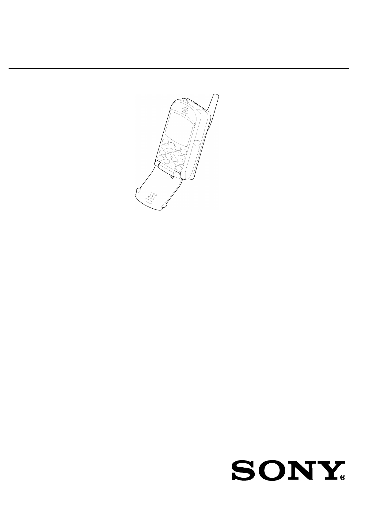
PORTABLE DIGITAL CELLULAR TELEPHONE
WITH ACCESSORIES
Page 2

Power requirements 4.0 V (nominal)
Operating temperature -10°C to +55°C
Accessories operating temperature ± 0°C to +45°C
Battery pack charging temperature ± 0°C to +40°C
Dimensions 90 x 50 x 30 mm
Weight 110 g (with Battery)
Supplied accessories AC Adapter QN-2TC
AC Cable UK
Battery Pack A-3627-234-A
Desktop Charger 1-476-508-11
Headphones 1-542-459-11
Remote with Microphone 1-476-509-11
Memory Stick A-7094-682-A
Carry Bag 3-230-059-01
Optical Audio Cable 1-757-888-11
Analog Audio Cable 1-823-050-11
Optional accessories Cigar Lighter Charger QN-2CC
Handsfree kit QN-MZ5HFK
EasyCom (SoftModem) QN-2EC
PC-Card QN-2PCM
Travel Charger QN-2TC
Design and specifications are subject to change without notice.
NOTE
This device contains electrostatically sensitive components. Damage can occur to these components
if the appropriate handling is not adhered to.
ESD Handling precautions:
A working area in which Digital Cellular Telephones may be safely handled without undue risk of
damage from electrostatic discharge must be available.
The area must be equipped as follows:
! All working surfaces must have a dissipative bench mat, safe for use with live equipment,
resistor to a common ground point.
connected via 1.2M
! A quick release skin contact device with a flexible cord, which has a built-in safety resistor of
a range between 5.2K
dissipative earth point.
! All containers and storage must be of the conductive type.
Ω
and 1.2MΩ shall be used. The flexible cord must be attached to a
Ω
2
Page 3

Batteries:
This device contains an internal battery in addition to the external battery pack. These batteries
are recyclable and should be disposed of in accordance with national legislation. They must not
be incinerated, or disposed of as ordinary rubbish.
CAUTION
Danger of explosion if battery is incorrectly replaced.
Replace only with the same or equivalent type
recommended by the manufacturer.
Discard used batteries according to the
manufacturer’s instructions.
ADVARSEL!
Lithiumbatteri-Eksplosionsfare ved fejlagtig håndtering.
Udskiftning må kun ske med batteri af samme fabrikat
og type.
Levér det brugte batteri tilbage til leverandøren.
ADVARSEL
Eksplosjonsfare ved feilaktig skifte av batteri.
Benytt samme batteritype eller en tilsvarende type
anbefalt av apparatfabrikanten.
Brukte batterier kasseres i henhold til fabrikantens
instruksjoner.
VARNING
Explosionsfara vid felaktigt batteribyte.
Använd samma batterityp eller en likvärdig typ som
rekommenderas av apparattillverkaren.
Kassera använt batteri enligt gällande föreskrifter.
VAROITUS
Paristo voi räjähtää, jos se on virheellisesti
asennettu. Vaihda paristo ainoastaan laitevalmistajan
suosittelemaan tyyppiin. Hävitä käytetty paristo
valmistajan ohjeiden mukaisesti.
3
Page 4

TABLE OF CONTENTS
SECTION 1
Specifications ……………………………………………………… (see Cover sheet)
SECTION 2
General Descriptions
2.1 Multi Band …………………………………………………….…. 06
2.2 Real Time Clock (RTC)…………………...……………...……..06
2.3 Vibra Alert Functionality ……………………………………..….06
2.4 Battery Safety ……………………………………………………06
2.5 Battery Charging ……..……………………………….…………07
2.6 Accessory Interface …………………………………….……… 07-08
2.7 RF Antenna connector / antenna switch ….……...………….. 08
2.8 Languages ..……………………………………………………...09
2.9 Memory stick ..…………………………………………………...09
SECTION 3
Available Accessories
3.1 Hands free kit QN-MZ5 HFK……………….……….. 10
3.2 Ciger Lighter Charger QN-2 CC ……………………..……… 10
3.3 AC Adapter QN-2 TC …………….………………. 10
3.4 EasyCom (SoftModem) QN-2 EC …………………….………. 10
3.5 PCMCIA Card QN-2 PCM ………………..……..….. 10
3.6 Desktop Charger (not for sale by itself) …………………….... 11
3.7 Standard Battery QN-MZ5 (not for sale by itself) ..…. 11
3.8 Magic Gate Memory Stick ………………...……………....…...11
3.9 Headphones (not for sale by itself) ………………...…….….. 11
3.10 Remote with Microphone (not for sale by itself) …………... 11
3.11 Optical Cable (not for sale by itself) ……………….………... 11
3.12 Carry Bag (not for sale by itself) ……………………..……... 11
3.13 Analog Audio Cable (not for sale by itself) …………….…… 11
4.2 The Basic Features of Your Phone …………………...……....13-15
SECTION 4
Operating Instructions
4.1 Parts and Controls ……………………………………………....12-13
4.3 Icon Glossary………………………………………..……………16
4.4 Menu Overview…………………………….…….….…………...17-18
SECTION 5
Disassembling / Testing
5.1 Disassembly ..…………………………………………………… 19-21
5.2 Interface to GSM-Tester ..…...……………………….……….. 22-23
5.3 Jigs & Tools .………………………………………..…………… 23
SECTION 6
Programming Instructions
6.1 Requirement …….……………………………………...………..24
6.2 Hardware set-up …..…………………………………...………..24
6.3 Software set-up …………………………………………….……24
6.3.1 Download Software to Mobile …...…….………………..… 24-25
6.3.2 Save Personal Data In Mobile…………..…….……...…… 25
4
Page 5

SECTION 7
Diagrams
7.1 RF Block …….…………………………………….…………….. 26
7.1.1 Block Diagram …...…….………………………………....…26
7.1.2 Operational Description…………...……..…….……...……27-28
7.2 Base Band Block ……….……………………………...………..29
7.2.1 Block Diagram (1/2) ..….………………………………....…29
7.2.2 Block Diagram (2/2)…………...……..…….…….…….……30
7.2.3 Operational Description…………...……..…….……...……31
7.3 Memory Stick Block ………....………………………...………..32
7.3.1 Block Diagram (1/2) ..….………………………………....…32
7.3.2 Block Diagram (2/2)…………...……..…….…….…….……33
7.3.3 Operational Description…………...……..…….……...……34
SECTION 8
Spare Parts and Accessories List
8.1 Spare Parts …….………………………………………….……..35
8.2 Accessories List …….…………………………………….……..36
5
Page 6

SECTION 2
GENERAL DESCRIPTIONS
2.1 Multi-band :
CMD-MZ5 support E-GSM 900 and DCS 1800 multi-band functionality.
Because the usage of multi-band depends on network capabilities, the phone is able to operate as a single band
mobile in GSM 900 as well as in DCS 1800; In addition, it supports the extra functionality required for multi-band
mobile stations: Inter-band/“seamless” hand-over, channel assignment, cell selection and re-selection, all between
both bands within a Public Land Mobile Network.
The manual and automatic PLMN selection in both bands is given.
The user does not need any special action to use the multi-band functionality of the phone.
Users are able to manually roam between PLMN’s operating in GSM 900 and DCS 1800 bands.
The CMD-MZ5 is a phase II, GSM 900 class 4, DCS 1800 class 1 mobile phone.
The nominal maximum output power for GSM 900 is 2W, for DCS 1800 1W.
2.2 Real Time Clock (RTC)
The real time clock is integrated into phone.
When the mobile is switched on the RTC is powered via the CPP.
When the phone is powered down, the RTC is powered from the main battery via its own low quiescent current
regulator.
When the main battery is low or removed, a back-up battery keeps the clock alive.
2.3 Vibra Alert Functionality
The vibrator is a 1.3V device.
A general port pin of the SC1 controls the switch mode of the vibration motor. It is powered through a regulator by
an interface control unit. If the mobile is in the phase of switching on or off the vibrator is off at all times.
2.4 Battery Safety
The battery pack contains a safety circuitry. The charging circuitry and the safety circuitry together guarantee a
double fail-safe battery pack. This means that each component can be either short or open and still all the safety
requirements will not be violated.
The safety concept protects against:
Over voltage
when Vbat falls below 4.06V - 4.15V.
Under voltage
Charging is still possible.
: The charging is stopped when Battery Voltage (Vbat) reaches 4.24V- 4.3V. The charging resumes
: When the cell voltage drops below 2.5V - 2.7V the cell is disconnected for discharging.
6
Page 7
2.5 Battery Charging
Standard Battery 620mAh typical Li-ion 1-476-508-11
The phone can be charged even during making phone calls.
However, the shortest charging time will be reached when the phone is switched off.
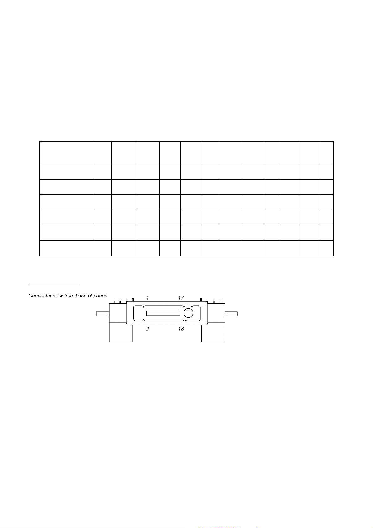
2.6 Accessory Interface
The table explains what kind of pins the phone supplies to the different accessories.
GND
Pins
AC-Adapter
(QN-2TC)
CLC
(QN-2CC)
Desktop Charger
(1-476-508-11)
HFK
(QN-MZ5HFK)
PCMCIA
(QN-2PCM)
EasyCom
(QN-2EC)
Connector layout
Charge
18
√ √
√ √
√ √
√ √ √ √ √ √ √
√
√
1/2
ACC
Power
Audio
3
√
√
Audio
IN
14
Out
13
ACC
ACC
ID
Detect
11
√ √ √ √
√ √ √ √
6
TX
(OUT)
9
RX
(IN)
10
Audio
GND
12
RF
RF
GND
19/22
√ √ √
20
7
Page 8

The Connector Comprises the following pins:
Detection
The detection of accessory is done by the charge pin and the detect pin.
Any accessory with an active charge will wake up the phone, indicating the battery icon but cannot be operated.
The insertion and removal of the charger (Cigar Lighter Charger, Desktop-Charger, AC-Charger) is detected by the
charge voltage.
The insertion and removal of other accessory is detected via an Interrupt. This detection is only possible when the
phone is powered up.
ID:
The ID pin indicates what kind of accessory is connected.
ACC power:
ACC-power has different functionality with different accessories. ACC-power supplies will be used as a signaling
pin for the Hands Free Kit.
In the car-kit environment the ext. Vbat indicates that a phone call is accepted/in progress. This information is used
by the car-kit to power up the audio section of the car-kit, mute the car stereo and keep the car-kit powered up
even when the ignition is switched off.
RX and TX:
This is the communication interface to the PCMCIA card “QN-2PCM” or the PC-link cable “QN-2EC”.
Audio In and Audio Out
These pins build the audio interface to the Head-Set and the Hands Free Kit.
Audio IN:
To limit the noise which is coupled on the Mic-line, the Mic amplifier in the Hands Free Kit “QN-MZ5HFK”.
Audio OUT:
The single ended output delivers 350mV into a 10kW load.
:
2.7 RF Antenna connector / antenna switch
To connect an external antenna for accessory use, the CMD-MZ5 contains a stable RF connector with an
integrated mechanical switch. This connector is placed on the I/O connector. The integrated mechanical switch
switches between the helix antenna and the external RF antenna connection. The switching criterion is mechanical
pressure from the RF accessory connector.
8
Page 9

2.8 Languages
The CMD-MZ5 supports the following languages:
• Dutch • German • Spanish
• English • Italian
• French • Portuguese
2.9 Memory stick
# You can record sound data onto the memory stick at the bitrate of 132kbps, 105kbps and 66kbps by Optical
input or Analog input.
# Receiving an incoming call is stopped during recording sound (to keep good sound quality).
# You can playback sound (data) recording onto the memory stick.
# The Play Settings function allows you to select how to play back such as Bass, AVLS, and Repeat (Shuffle).
# Selecting the next track, the previous track, going forward, backward and stop are available.
# When you receive an incoming call during playback, playback is stopped automatically and the Ringer is heard
from the headphones. An incoming call is received with pressing the answering / ending call button on the
remote.
# To end, keep the answering / ending call button on the remote pressed.
# Playback sound can be stopped by pressing the answer / ending call button on the remote during playback.
# Also, to start playback, press the answer / ending call button on the remote.
# When WAP is being used, you can not playback sound recorded onto the memory stick.
9
Page 10
SECTION 3
AVAILABLE ACCESSORIES
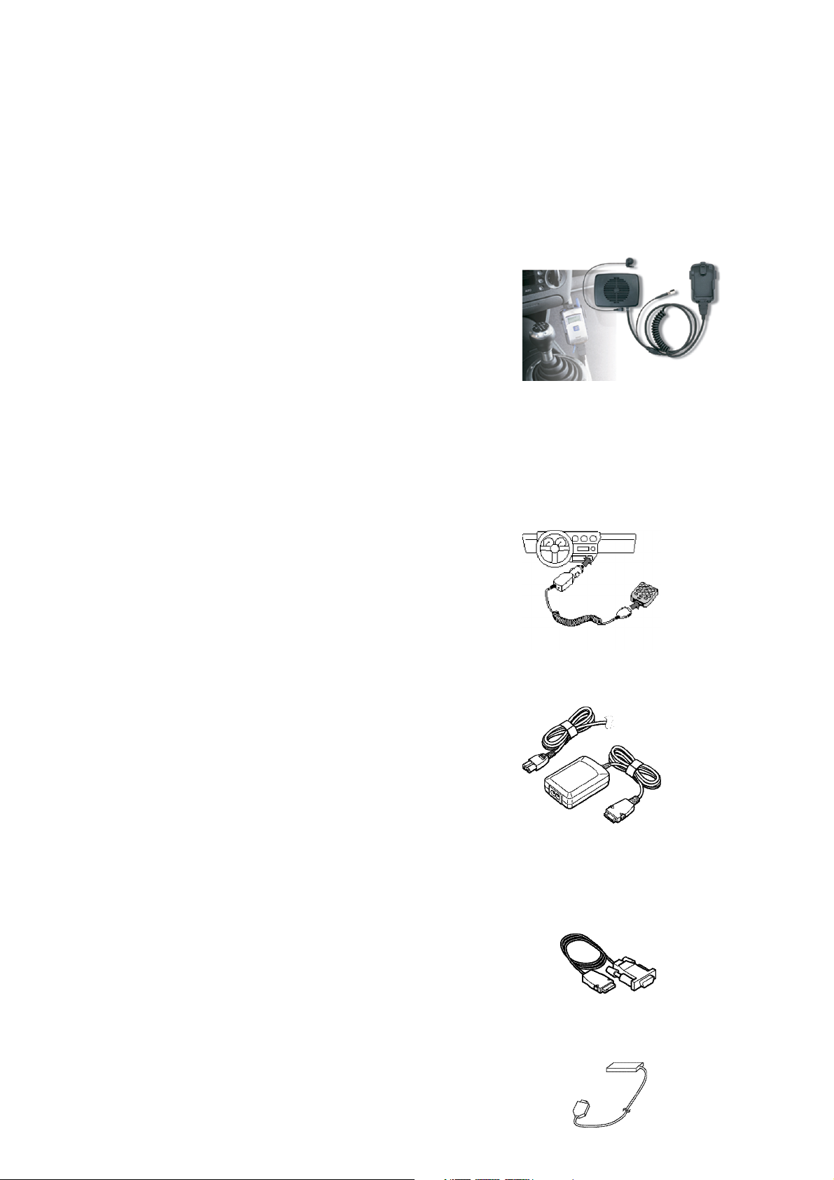
3.1 Hands Free Kit
The Hands Free Car Kit QN-MZ5HFK is designed to offer superior speech quality and Full Duplex speech transmission.
In Full Duplex operation both parties can speak simultaneously. The cradle secures a safe hold of the phone. The Car
Kit has a RF connector for the use of an external antenna to offer a high quality radio link to the base station.
Specifications:
Input voltage DC 12V, negative ground
Rated output voltage 5.0V
Rated output current 500mA
3.2 Cigar Lighter Charger
The QN-2CC Cigar Lighter Charger is an additional charging option or alternative for the standard charger and only for
use in vehicles equipped with a 12 volt negative ground electrical system. This Charger is intended for charging
purposes only and not for making/receiving phone calls in the car.
Charging Time:
Full charging can take up to ~3 hours, but will be longer if the CMD-MZ5 is switched on or if the temperature is outside
the 0°C - 45°C operating range.
Specifications:
Input voltage DC 12V, negative ground
Rated output voltage 5.0V
Rated output current 500mA
3.3 AC Adapter
The Power Adapter QN-2TC is a small and lightweight device. It has a full Input Voltage Range from 110-240Volts.
Using a standard cable makes the connection to the main socket.
Specifications:
Input voltage 110 to 240 V
Rated output voltage 5.0V
Rated output current 500mA
3.4 EasyCom (Soft Modem)
The EasyCom QN-2EC Data Cable connects the phone to a PC via a RS 232 cable. It supports SMS as well as Full
Data/Fax Capability 9.6 Kbps. The phonebook management application bundled on the CD can not be used with CMDMZ5.
This configuration is available for Windows 95/98.
3.5 PCMCIA Card
The functionality of the PC Card QN-2PCM is the same as the Data Cable QN-2EC. But it supports both GSM
connections up to 9.6 Kbps and PSTN connections up to 56 Kbps.
For Windows 95, 98, Windows NT, Mac OS.
10
Page 11
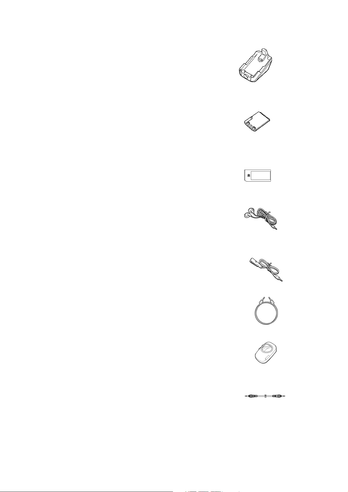
3.6 Desktop Charger
(not for sale by itself)
The desktop charger can charge either the Standard 1-476-508-11 with the phone attached. The Desk Top
Charger gets its power supply via the Power adapter QN-2TC.
Specifications:
Input voltage DC 5V
Rated output voltage 5.0V
Rated output current 500mA
3.7 Standard Battery
(not for sale by itself)
Specifications:
Lithium Ion Battery A-3627-234-A (QN-MZ5BPS)
Maximum output voltage DC 4.2V
Nominal output voltage DC 4.0V
Capacity 620mAh
3.8 Magic Gate Memory Stick
3.9 Headphones
(1-542-459-11) (not for sale by itself)
Ø 3.5 stereo mini plug
3.10 Remote with Microphone
(1-476-509-11) (not for sale by itself)
3.11 Optical Cable
3.12 Carry Bag
(1-757-888-11) (not for sale by itself)
(3-230-059-01) (not for sale by itself)
3.13 Analog Audio Cable
(1-823-050-11) (not for sale by itself)
11
Page 12
SECTION 4
OPERATING INSTRUCTIONS
This section provides a brief guide to the operation and facilities available on the CMD-MZ5.
Refer to the Operating Manual for full operational information.
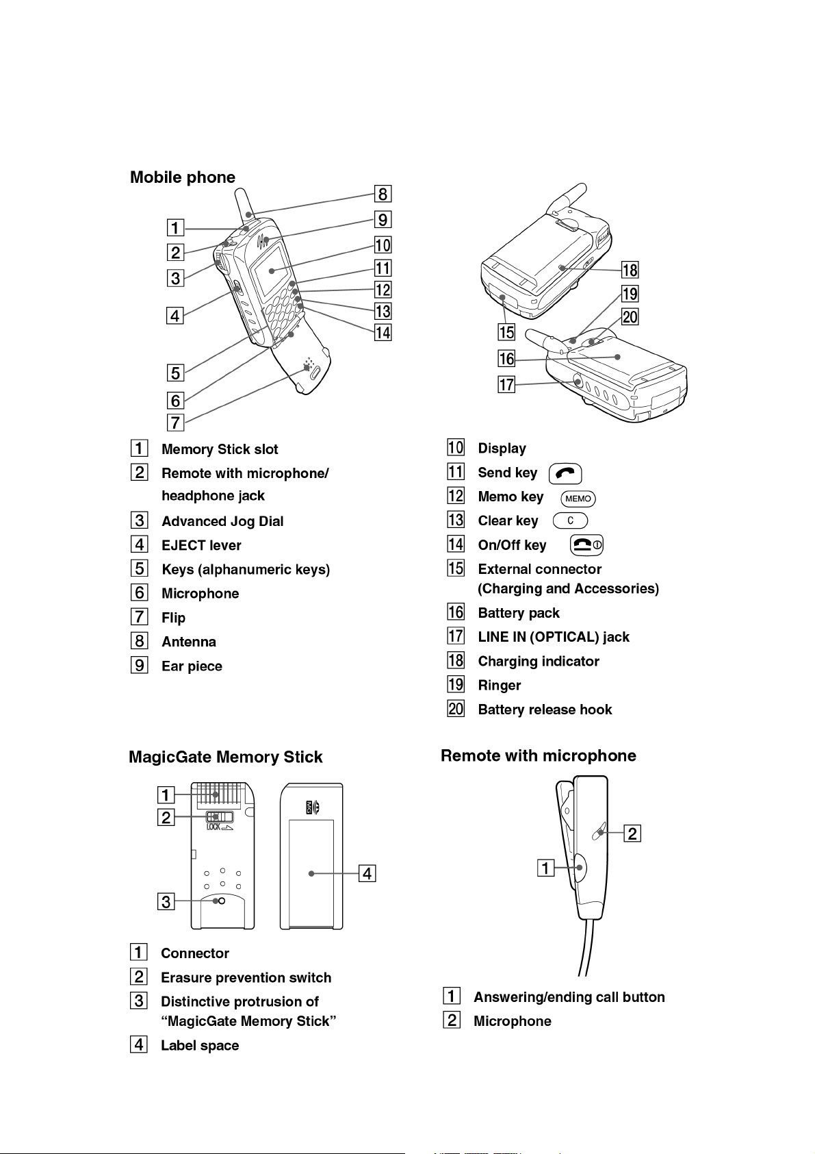
4.1 Parts and Controls
12
Page 13

4.2 The Basic Features of Your Phone
13
Page 14

14
Page 15

15
Page 16

4.3 Icon Glossary
16
Page 17

4.4 Menu Overview
17
Page 18

18
Page 19

SECTION 5
DISASSEMBLING / TESTING
5.1 Disassembly
IMPORTANT NOTE :
The IMEI Sticker mounted on the MS board (visible from the battery compartment) should not be removed at all.
The IMEI number is the electronic identification of the hardware, and it is stored electronically.
There should be no discrepancy between the number on the sticker and the number within the set logic allowed.
Follow the disassembly procedure in the numerical order given.
CABINET (FRONT) SUB ASSY
LCD
19
Page 20

MEMORY STICK CONNECTOR
BOARD ASSY
20
Page 21

SHIELD ASSY
MS BOARD, MAIN BOARD
Re-assembly procedure :
To re-assemble the unit, apply the reverse order of the above mention disassembly procedure.
21
Page 22

5.2 Interface to GSM-Tester
Test Set Up for CMD-MZ5 Level 1 Testing
Use special RF-Adapter for connection of STC-02 to your GSM –Tester !
*
CMD-MZ5
+
Battery Pack
+
Test SIM Card
Service Test Connector
RF input Connector *
RF output :
SMA plug
STC-02 Part No.
1-792-726-11
*
GSM – TESTER
This unit acts as a base station providing
all the necessary GSM signalling
requirements and provides GSM signal
measuring facilities as well.
22
Page 23

Level Test Procedure with GSM TESTER recommendation:
• Simulate GSM call processing – to check the functionality of transmitting and receive audio signals
of loudspeaker and microphone.
• Basic GSM transmission & reception parameter testing – to ensure that handset’s performance
compiles with standard GSM specification.
5.3 Jigs & Tools
Description Part No Remark
DATA TRANSFER JIG DTJ-01 1-792-172-11 Necessary For Software Update
HOOK RELEASE JIG 3-043-180-01 For Housing Opening
SERVICE TEST CONNECTOR
DATA TRANSFER JIG
STC-02
3-224-391-01
HOOK RELEASE JIG
For Connection To GSM Measure
Equipment
SERVICE TEST CONNECTOR
23
Page 24

SECTION 6
PROGRAMMING INSTRUCTIONS
6.1 Requirement
• PC (486 type or higher) with Microsoft “Windows” Operating System
• One COM-port free for usage
• The Data Transfer Jig (unit: p/n 1-792-172-11)
PREPARATION FOR SOFTWARE UPDATE
DATA
TRANSFER
6.2 Hardware set-up
• Copy all the files to the PC (define own directory).
• Connect the Data Transfer Jig to the PC COM-port (COM 1 or COM 2) and the CMD-MZ5 external connector.
• Attach battery pack to CMD-MZ5; the CMD-MZ5 is powered up from the battery pack.
• The initial settings of the flash.exe program may not correspond with the normally correct settings. It is highly
advisable to check the settings first (see 6.3 Software set-up).
6.3 Software set-up
6.3.1 ∗ Download Software to Mobile (Software Update)
• Start the program flash.exe by double-clicking on its icon in the Windows Explorer.
• Check if the settings for the “Com Port”, “Speed” and “Load Option” are correct.
Com Port : COM 1
Baud Rate : 115200
Load Option : DOWNLOAD TO MOBILE
MZ5 Flash.exe
24
Page 25

Settings can be saved to “flash.ini” in the windows directory.
• Click on “Start” and select an SRE file for downloading.
• Switch on the CMD-MZ5.
• Now the program run automatically.
6.3.2 * Save Personal Data in Mobile
The set-up and all requirements for this data transfer are the same as for the software update.
• Check if the settings for the “Com Port” , “Speed” and “Load Option” are correct.
− The CMD-MZ5 software is located in the MZ5. SRE file.
− Any other SRE file is either only needed for the program itself, or can be a personal data file (see below).
There are 3 kinds of SRE files: - “MZ5.sre” for actual software download
- “xxx.sre” for personal data download (see blow)
- “ flash.sre” is an application software (do not use / modify)
− Flash erase area is automatically calculated with the contents of the life.
Com Port : COM 1
Speed : 115200
Load Option : SAVE DATA FROM MOBILE
• Click on “Start”
• Select or input file to save data.
• Switch on the CMD-MZ5.
• Save read data in the selected file.
The read data can be downloaded to the Mobile with this loader as described above.
25
Page 26

SECTION 7
7.1 RF Block
7.1.1 Block Diagram
DIAGRAMS
26
Page 27

7.1.2 Operational Description
(1) Receiver Section
Radio signals received from the antenna located on the top of cabinet enter the RF connector of common
connector (CN401) provided at the bottom of cabinet.
After they are separated from the signals coming from external units by a mechanical switch, they enter the
antenna switch module (CP702). This module separates the signals transmitted/received to/from the antenna by
means of the switch, and also selects GSM or DCS band. The received signals are separated here into GSM side
and DCS side.
The received signals in the GSM band pass through the band-pass filter (SWF702) from CP702 to remove the
signals out of the receiving band. Then, the received signals are amplified in the low-noise amplifier using the
transistor (Q702).
Further, the band-pass filter (SWF704) removes unnecessary signals out of the band.
The SWF704 output signals are balanced signals. Thus, the signals from band-pass filter can be entered as
balanced signals to the subsequent RF IC CXA3200ER (IC604) having a balanced input system.
Similarly, the received signals in the DCS band pass through the band-pass filter (FL701) from CP702 to remove
the signals out of the receiving band. Then, the received signals are amplified in the low-noise amplifier using the
transistor (Q701), and further the band-pass filter (SWF703) removes unnecessary signals out of the band. Same
as in GSM band, the SWF703 output signals are also balanced signals, so that they can be entered to the IC604
as they are. FL701 is a dielectric filter, while SWF702 to SWF704 are all SAW filters.
To prevent characteristic deterioration due to bias point fluctuation at high temperature, the Q701 and Q702
detect current flowing in the transistors using signals at pins 37 to 39 of IC604 and perform the feedback control
so that the current flowing in the transistors is constant at all times.
Respective input signals in GSM and DCS bands entered to the IC604 are entered to the receiving mixer in the
IC604. They are mixed with local signals from VCO601 in the mixer and converted into IF signals in the 440MHz
band. The output of IF signals passes through the band-pass filter (SWF601) where unnecessary signals are
removed. The SWF601 output signals return to the IC604 again.
The SWF601 input/output signals are all balanced signals. The signals in the 440MHz band that returned to the
IC604 are adjusted to proper level signals by variable gain amplifier (PGC) in the IC604, and then they are
orthogonal-demodulated with 440MHz signal obtained by dividing the oscillation frequency 880MHz by two at the
signal reception from VCO602, and they become base band IQ signals in the IC604.
The received signals that became base band IQ signals pass through low-pass filter in the IC604 to remove
unnecessary signals, and then they are sent to the base band side.
The signals sent to the base band side are IQ signals having 1.4V DC offset.
(2) Transmitter Section
IQ signals transmitted from base band side are modulated into signals in the transmission IF frequency band by
an orthogonal modulator in the IC604. IQ signals must have DC offset voltage 1.575V typ. and signal amplitude
500mVp-p. The transmission IF frequency is 195MHz (975MHz/5) when the terminal is in GSM mode, or 325MHz
(975MHz/3) in DCS mode. By this modulation, local signals are generated by dividing the oscillation frequency
(975MHz) by an internal frequency divider (3/5 switching) at the signal transmission from VCO602.
The modulated signals outputted from orthogonal modulator pass through low-pass filter in the IC604, and then
they enter the phase comparator of the offset loop system modulator.
In the offset loop system modulation, the VCO having same oscillation frequency as transmission frequency is
assembled in the phase lock loop, and the reference frequency of this phase lock loop is used as transmission IF
frequency to adjust the phase shift of VCO to that of transmission IF frequency. As a result, the same effect as if
the phase modulation was applied to the transmission frequency can be attained.
Also, the transmission frequency can be selected simultaneously by using the output of VCO mixed down with the
frequency divided by VCO601 as a comparison frequency of the phase lock loop.
Unlike conventional mix up system, this offset loop system can reduce spurious signals generated in the mixer.
The output signals of offset loop are converted into the GMSK modulated signals by the power VCO, VCO801.
This VCO has two outputs of GSM band and DCS band, and the operation modes can be switched by signal lines.
The output of VCO801 is already GMSK modulated waves of transmission frequency. The output of VCO801 in
the GSM band passes through the low-pass filter FL805 where harmonic component is attenuated. As the PA
module CP803 has only one input, this output is composed into one in the diplexer FL806. Also, a part of signals
returns to the IC604 for the input of phase lock loop. The output of FL806 enters the PA module CP803 via the
matching circuit. The CP803 is a power amplifier having dual bands, and which frequency is to be outputted is
switched over by the signal lines.
This power amplifier has output controllable terminals, so that the output voltage can be controlled according to
external voltage.
The CP803 generates two outputs, GSM and DCS.
27
Page 28

These two outputs pass through low-pass filters CP801 and 802 respectively to remove harmonic component.
These CP801 and 802 are also used as directional couplers to detect a part of the power amplifier output for the
power control. The outputs of CP801 and 802 are entered to the front-end module CP702. This module switches
over the transmission, reception, and band, as mentioned previously. The signals entered to the CP702 are
outputted from the antenna via reversed route of received signals.
The signals detected in the CP801 and 802 are entered to the D803 and D802 respectively, and they are rectified
to become DC voltage components. These outputs are composed into one, and it is compared with APC signal
from base band in the operation amplifier IC801 to be the signal to control the CP803 so that the output voltage
can follow the APC signal.
(3) PLL Section
The PLL block consists of dual PLL (IC601) and VCO601 and VCO602. The VCO601 is for channel PLL and
generates thefollowing oscillation frequencies.
GSM band
The output of VCO601 is entered to the FL601 and distributed to two outputs. One of these outputs returns to the
IC601, and another output is entered to the IC604. In the transmission of GSM band, the signal entered to the
IC604 is divided into two internally, and therefore the frequencies of every 400kHz step are used in this case only.
The VCO602 is for local PLL and generates the following oscillation frequencies.
Transmission : 975MHz
Reception : 880MHz
At the signal transmission, 975MHz is divided into five in the GSM band, or three in the DCS band in the IC604.
At the signal reception, 880MHz is always divided into two in the IC604.
Each VCO is provided with an external switching transistor so as to control the power supply.
(4) TCXO Section
The X601 is a VCTCXO module and it oscillates 13MHz reference signal. This oscillation frequency can be finely
adjusted by AFC signal from the DSP. The output signal of X601 is given to the IC601 as it is, and also buffered
in the Q602 and then supplied to the base band.
(5) Power Supply Section
The power supply voltage given from the battery side is supplied directly to the power amplifier module (CP803).
For other blocks, the power is supplied from the regulator ICs, IC501 and IC502.
The IC501 supplies 2.8V to the PLL block, while the IC502 supplies 2.8V to other blocks.
Transmission 1370.4 – 1439.6MHz 400kHz step
Reception 1365.2 – 1399.8MHz 200kHz step
Transmission 1385.2 – 1459.8MHz 200kHz step DCS band
Reception 1365.2 – 1439.8MHz 200kHz step
28
Page 29

7.2 Base Band Block
7.2.1 Block Diagram (1/2)
29
Page 30

7.2.2 Block Diagram (2/2)
30
Page 31

7.2.3 Operational Description
(1) IC102 (1689WG72RME15IR-DT)
This device provides the functions such as DSP1600 core, ADC, DAC, ROM, RAM, serial port, parallel host
interface, two timers, and error correction coprocessor (ECCP). This device is connected to the system controller,
RF, and Mic & Speaker to perform RF control and input/output of audio signals. As the operation clock, it uses
13MHz from the VCTCXO.
(2) IC101 (48010WGORAB38KY-DT)
This device provides the functions such as 32bit RISC processor, on-chip RAM, DMA, synchronous serial
interface, asynchronous serial interface, interrupt controller, SIM interface, timer, and ADC.
This device performs system control. As the operation clock, it uses 13MHz from the VCTCXO.
(3) IC103 (MB84VD22182EE) (ROM/RAM)
A flash type ROM with the capacity of 32Mbits is used. The RAM capacity is 4Mbits. The data bus width is 16 bits
or 8 bits. Here, the programs and telephone directory data are stored.
(4) IC104 (BU16303-0GE2)
This device provides the functions such as key scanning, interrupt extension, power supply circuit control, watch
dog timer, voltage monitoring, and output port extension. It is connected to the system controller (IC101) data bus.
(5) IC203 (ISD5008ZD)
This device provides the audio signal recording and playing function and also the audio path switching function. It
is capable of recording for 4 minutes at 8kHz sampling. It is subject to synchronous serial control by the system
controller (IC101).
(6) IC301 (BH6022FV)
This device is a system power supply with the built-in three regulators, two voltage detectors, one vibrator driver,
and three FETs.
(7) IC201 (RV5C338A)
This device is a real time clock. It is subject to synchronous serial control by the system controller (IC101). This
real time clock outputs 32kHz clock, and supplies it to the IC101, IC102 and IC104.
(8) LCD1 (LCD Module)
The specifications of this liquid crystal display are as follows.
Glass size: 38mm x 31.5mm
Number of dots: 96x72 dots
LCD driver: HD66728
The LCD is connected to the system controller (IC101) data bus.
31
Page 32

7.3 Memory Stick Block
7.3.1 Block Diagram (1/2)
32
Page 33

7.3.2 Block Diagram (2/2)
33
Page 34

7.3.3 Operational Description
(1) Memory Stick Bock Configuration
The memory stick block consists of a CPU (IC101) with the built-in ARM 7 cores + MS I/F, digital signal
processing IC (IC301), magic gate IC (IC401), audio path control IC (IC601), A/D and D/A converter (IC501),
digital audio I/F (IC801), headphone amplifier (IC701), S-RAM (IC201), CMOS regulator (IC901, IC902, IC903,
IC904), SIM I/F (IC205), optical connector, remote control jack, and 64M memory stick.
(2) Audio Compression and Expansion Section
The audio data are compressed and expanded in the digital signal processing IC (IC301) to support the SDMI
(Water Mark compatible). For this purpose, the ATRAC3 system is used, and the compressed data are encrypted
in the magic gate IC (IC401), and stored in the memory stick. Also, the expanded data are D/A-converted, and its
low frequency components are amplified in the headphone amplifier (IC701) via audio path control IC (IC601),
then outputted to the headphone.
(3) Magic Gate Section
The memory stick recognition is made between magic gage IC (IC401) and magic gate IC in the memory stick via
CPU so as to check the memory stick for magic gate compatibility.
Further, at the recording, music data compressed in the digital signal processing IC (IC301) are encrypted and
stored in the memory stick.
Also, at the playing, the encrypted data in the memory stick are decrypted and led to the digital signal processing
IC (IC301).
(4) Audio Path Control Section
The output paths of received audio, played back audio, terminating tone and key tone are switched over to the
receiver, headphone, or earphone, and audio signals are mixed and the volume is controlled, then the signals are
led to the headphone amplifier.
(5) Digital Recording Section
Optical digital audio signals entered from optical connector are synchronized in the digital audio interface (IC801)
and demodulated into normal format, and led to the digital signal processing IC (IC301) and compressed there.
Then, they are encrypted in the magic gate IC (IC401) and stored in the memory stick.
(6) Analog Recording Section
Analog audio signals entered from optical connector are A/D-converted and led to the digital signal processing IC
(IC301) and compressed there, and then they are encrypted in the magic gate IC (IC401) and stored in the
memory stick.
(7) SIM Interface Section (IC205 (PSC1515))
This device is a SIM interface IC with the built-in charge pump so as to support both 3V and 5V SIMs.
(8) Remote Control Section
The remote controller is equipped with the TEL key for originating a call and answering a terminating call, and the
microphone for the talk through earphone and the headphone output line.
The headphone output line is provided with a (φ3.5 stereo mini pin jack, and commercial headphones can also be
used.
34
Page 35

SECTION 8
SPARE PARTS AND ACCESSORIES LIST
8.1 Spare Parts
Note:
•
The parts with no reference in the exploded view are not supplied.
Ref. No.
1 A-3649-273-A CABINET (FLIP) ASSY
2 1-542-424-11 MICROPHONE
3 A-3649-272-A CABINET (FRONT) SUB ASSY
4 3-229-711-01 ASSY (L), BEARING
5 3-229-712-01 ASSY (R), BEARING
6 3-226-472-01 SPACER (HINGE)
7 1-786-161-11 SWITCH, RUBBER KEY
8 X-3378-891-1 LIGHT GUIDE ASSY
9 3-226-146-01 COVER, EARPHONE
10 A-3622-524-A FLEXBLE MOUNT ASSY
11 3-226-135-01 SCREW (1.4X3.5), PRECISION
12 1-815-290-11 CONNECTOR, MEMORY STICK
13 A-3649-270-A CABINET (REAR) ASSY
14 3-926-356-01 SCREW, ROTARY SWITCH
15 A-3627-234-A BATTERY PACK
16 3-226-148-01 COVER, CONNECTOR
Part No. Description Remark Ref. No. Part No. Description Remark
17 1-528-999-11 BATTERY, BACK UP
18 1-418-983-11 JOG, CODER
19 3-046-962-01 CUSHION (VIBRA-MOTOR)
20 1-763-510-11 VIBRA-MOTOR
21 1-544-797-11 SPEAKER
22 3-226-473-01 CUSHION, SPEAKER
23 3-226-149-01 HOLDER, EARPHONE
24 3-226-150-01 GUIDE, MS
25 3-233-526-01 SPACER (VIBRATION)
26 3-226-144-01 COVER, MS
27 3-226-145-01 BUTTON, MS EJECT
ANT101 1-754-185-11 ANTENNA
CN205 1-815-291-11 CONNECTOR, SIM
CN901 1-815-292-11 CONNECTOR, BOARD TO BOARD
J801 1-815-288-11 JACK, CONNECTOR
LCD1 1-803-928-11 LCD
35
Page 36

8.2 Accessories List
Ref. No.
101 1-418-645-14 ADAPTOR, AC (AC-110-240V)
102 1-476-508-11 DESK TOP CHARGER
103 1-476-509-12 REMOTE CONTROL UNIT
104 1-542-459-12 HEADPHONE
105 1-757-888-11 CORD, CONNECTION
106 1-823-028-11 AC POWER-SUPPLY CORD SET (UK)
107 3-230-059-01 CARRY BAG
108 A-3627-234-A BATTERY PACK
109 A-7094-682-A MOMORY STICK
110 1-823-050-11 CORD, CONNECTION (ANALOG)
3-229-247-12 MANUAL, INSTRUCTION (ENGLISH)
3-047-243-11 HAND STRAP
Part No. Description Remark
36
Page 37

(Hong Kong)
9-870-403-21
Sony Corporation
Digital Telecommunications Network Company
Published by Quality Assurance Dept.
2001G0500-1
© 2001.7
37
 Loading...