

Page 1
CDX-C4900R/C5000R/C5000RX
AEP Model
UK Model
SERVICE MANUAL
SUPPLEMENT-2
File this supplement with the service manual.
Subject : Change of Main, Sub (CD) and Key Boards
(ECN-CSA01521/CSA02901)
TABLE OF CONTENTS
1. CHANGE OF MAIN, SUB (CD) AND KEY BO ARDS
1-1. Discrimination ........................................................2
1-2. Diagrams
• Printed Wiring Board –Main Section– ....................................... 4
• Schematic Diagram –Main Section (1/3)– ................................. 6
• Schematic Diagram –Main Section (2/3)– ................................. 7
• Schematic Diagram –Main Section (3/3)– ................................. 8
• Schematic Diagram –Sub (CD) Section–...................................9
• Printed Wiring Board –Sub (CD) Section– .............................. 10
• Printed Wiring Board –Key Section–.......................................11
• Schematic Diagram –Key Section– .........................................12
1-3. ELECTRICAL PARTS LIST .................................13
1
Page 2
1. Change of Main, Sub (CD) and Key Boards
When performing service and inspection, check the part number of
the main, sub (CD) and key boards.
1-1. Discrimination
-MAIN BOARD (COMPONENT SIDE)-
Main board part No.
Former:1-677-055-11
New :1-677-055-12
-SUB(CD) BOARD (COMPONENT SIDE)-
-KEY BOARD (COMPONENT SIDE)-
Sub(CD) board part No.
Former:1-677-056-11
New :1-677-056-12
Key board part No.
Former:1-676-602-12
New :1-676-602-13
2
Page 3

CDX-C4900R/C5000R/C5000RX
1-2. Diagrams
THIS NOTE IS COMMON FOR PRINTED WIRING
BOARDS AND SCHEMATIC DIAGRAMS.
(In addition to this, the necessary note is
printed in each block.)
• Refer to page.
( ) : Refer to page of supplement-2.
< > : Refer to page of service manual.
for schematic diagram:
• All capacitors are in µF unless otherwise noted. pF: µµF
50 WV or less are not indicated except for electrolytics
and tantalums.
• All resistors are in Ω and 1/
specified.
• % : indicates tolerance.
f
•
• C : panel designation.
• U : B+ Line.
• Power voltage is dc 14.4V and fed with regulated dc power
• Voltages are tak en with a V OM (Input impedance 10 MΩ).
• Waveforms are taken with a oscilloscope.
• Circled numbers refer to waveforms.
• Signal path.
: internal component.
supply from ACC and BATT cords.
Voltage variations may be noted due to normal produc-
tion tolerances.
Voltage variations may be noted due to normal produc-
tion tolerances.
F : FM
f : MW
J : CD
4
W or less unless otherwise
for printed wiring boards:
• X : parts extracted from the component side.
• Y : parts extracted from the conductor side.
a
•
• b : Pattern from the side which enables seeing.
Caution:
Pattern face side: Parts on the pattern face side seen from the
(Side B) pattern face are indicated.
Parts face side: Parts on the parts face side seen from the
(Side A) parts face are indicated.
: Through hole.
(The other layer’s patterns are not indicated.)
33
Page 4
CDX-C4900R/C5000R/C5000RX
• Semiconductor
Location (Side A)
Ref. No. Location
D1 E-9
D301 G-4
D501 I-7
D502 H-7
D551 J-13
D552 K-13
D553 K-13
D554 J-12
D555 K-13
D556 J-12
D557 K-13
D558 J-12
D559 K-13
D560 J-12
(D571) B-5
D603 B-4
(D605) B-5
D622 D-9
D624 C-9
D653 I-7
D661 D-5
D662 D-5
D673 C-5
D674 C-5
D701 E-5
D702 C-4
D703 B-3
D704 B-2
D705 B-2
D706 B-2
D708 G-7
D710 D-4
• PRINTED WIRING BOARD — MAIN SECTION —
IC51 I-12
IC90 H-11
IC151 D-10
IC501 I-5
IC652 J-3
IC701 C-3
Q1 G-11
Q171 B-11
Q181 B-11
Q271 C-11
Q281 C-11
Q363 I-3
Q365 G-2
Q551 J-6
(Q571) D-6
Q621 C-10
Q622 C-9
Q633 J-2
Q651 I-8
Q652 I-8
Q661 D-5
Q701 D-5
Q704 G-7
Q705 C-4
Q706 D-4
( ): CDX-C5000R/C5000RX only
44
Page 5
CDX-C4900R/C5000R/C5000RX
<Page 27>
• Semiconductor
Location (Side B)
Ref. No. Location
D2 E-8
D90 H-12
D91 H-11
D92 G-12
D302 G-8
D361 I-2
D362 G-2
D363 G-3
D561 K-11
D562 K-11
D601 C-3
D602 B-4
D604 A-5
D621 C-10
D631 J-2
D671 C-5
D672 C-5
D675 I-4
D676 I-4
D677 I-4
D709 G-5
(Page 10)
IC611 B-7
IC671 E-1
Q90 G-11
Q361 H-1
Q362 G-1
Q364 G-2
Q631 J-2
55
Page 6
CDX-C4900R/C5000R/C5000RX
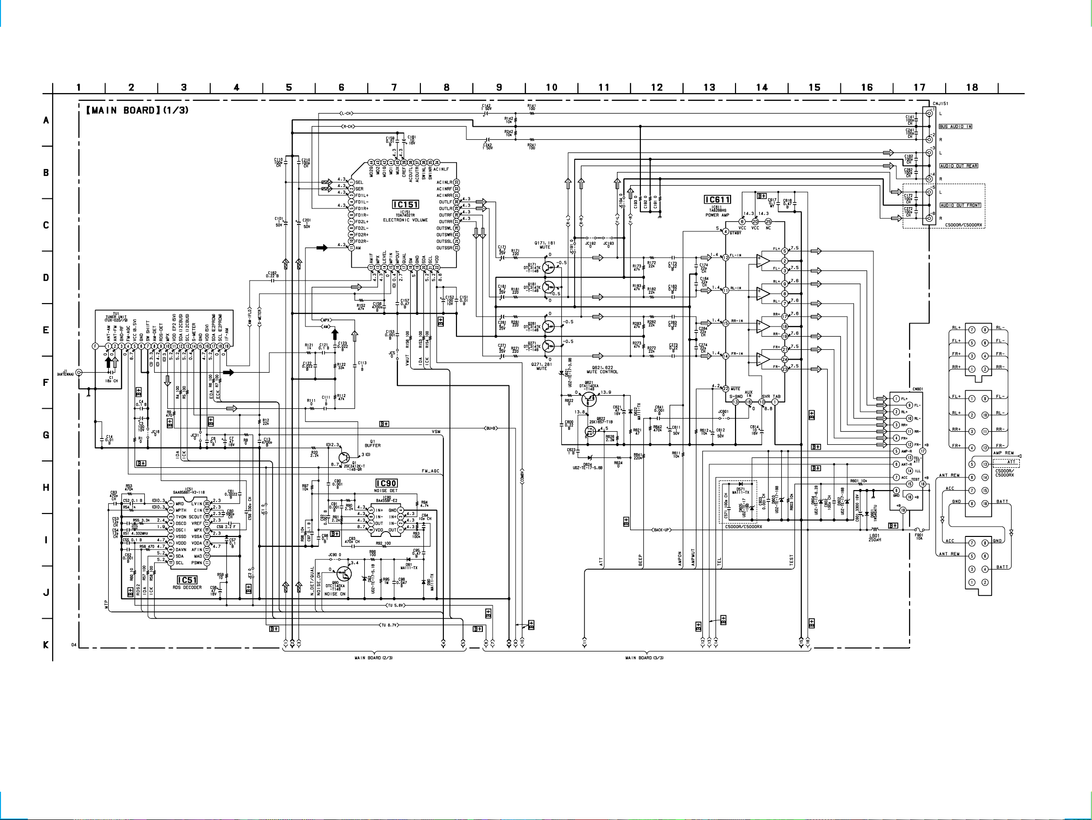
• SCHEMATIC DIAGRAM — MAIN SECTION (1/3) — • Refer to page 39 of Service manual for IC Block Diagrams.
(Page 7) (Page 8)
66
Note:
• Voltage is dc with respect to ground under no-signal
(detuned) condition.
no mark : FM
( ) : MW
Page 7

• SCHEMATIC DIAGRAM — MAIN SECTION (2/3) —
CDX-C4900R/C5000R/C5000RX
(Page 6)
<Page 28>
(Page 8)
77
Note:
• Voltage is dc with respect to ground under no-signal
(detuned) condition.
no mark : FM
( ) : MW
< > : CD PLAY
: Impossible to measure
∗
Page 8

CDX-C4900R/C5000R/C5000RX
• SCHEMATIC DIAGRAM — MAIN SECTION (3/3) — • Refer to page 39 of Service manual for IC Block Diagrams.
(Page 6)
(Page 7)
(Page 9)
Note:
• Voltage is dc with respect to ground under no-signal
(detuned) condition.
no mark : FM
( ) : MW
< > : CD PLAY
: Impossible to measure
∗
88
Page 9

• SCHEMATIC DIAGRAM — SUB (CD) SECTION —
(Page 8)
CDX-C4900R/C5000R/C5000RX
(Page 12)
99
Page 10

CDX-C4900R/C5000R/C5000RX
• PRINTED WIRING BOARD — SUB (CD) SECTION —
(Page 5)
(Page 11)
1010
Page 11

• PRINTED WIRING BOARD — KEY SECTION —
CDX-C4900R/C5000R/C5000RX
• Semiconductor Location
Ref. No. Location
(D901) A-11
(D902) B-10
(D903) B-10
(D904) B-10
(D951) C-4
(D952) B-6
(IC901) B-8
IC951 C-5
LED901 A-2
( ) : SIDE B
< > : SIDE B, CDX-C4900R/C5000R only
Ref. No. Location
LED902 C-2
LED903 C-4
LED904 A-4
LED910 B-12
LED911 B-12
LED912 A-5
LED913 B-5
<Q901> A-3
<Q902> A-3
(Page 10)
11 11
Page 12

CDX-C4900R/C5000R/C5000RX
• SCHEMATIC DIAGRAM — KEY SECTION —
(Page 9)
Note:
• Voltage is dc with respect to ground under no-signal
(detuned) condition.
no mark : FM
: Impossible to measure
∗
1212
Page 13

1-3. Electrical Parts List
NOTE:
• Due to standardization, replacements in
the parts list may be different from the
parts specified in the diagrams or the
components used on the set.
• -XX and -X mean standardized parts, so
they may have some difference from the
original one.
• RESISTORS
All resistors are in ohms.
METAL:Metal-film resistor.
METAL OXIDE: Metal oxide-film resistor.
F:nonflammable
Ref. No. Part No. Description Remark Ref. No. Part No. Description Remark
KEY BOARD
**********
1-694-660-11 CONDUCTIVE BOARD, CONNECTION
* 3-040-992-02 HOLDER (LCD)
* 3-040-993-01 PLATE (LCD), LIGHT GUIDE
* 3-040-997-02 PLATE (LCD), GROUND
3-041-371-11 SHEET (REFLECTOR)
< CAPACITOR >
C951 1-164-004-11 CERAMIC CHIP 0.1uF 10% 25V
C952 1-163-037-11 CERAMIC CHIP 0.022uF 10% 25V
C953 1-163-251-11 CERAMIC CHIP 100PF 5% 50V
C954 1-164-004-11 CERAMIC CHIP 0.1uF 10% 25V
C955 1-164-004-11 CERAMIC CHIP 0.1uF 10% 25V
C956 1-164-489-11 CERAMIC CHIP 0.22uF 10% 16V
< CONNECTOR >
• Items marked “*” are not stocked since
they are seldom required for routine service.
Some delay should be anticipated
when ordering these items.
• SEMICONDUCTORS
In each case, u : µ, for example:
uA.. : µA.. uPA.. : µPA..
uPB.. : µPB.. uPC.. : µPC.. uPD.. : µPD..
• CAPACITORS
uF : µF
• COILS
uH : µH
LED904 8-719-061-16 LED CL-190SR-CD-T (C5000RX)
LED904 8-719-078-15 LED CL-165Y/PG-D-T (C4900R/C5000R)
LED910 8-719-078-19 LED LWA673-R1S2
LED911 8-719-078-19 LED LWA673-R1S2
LED912 8-719-078-19 LED LWA673-R1S2
LED913 8-719-078-19 LED LWA673-R1S2
LSW901 1-771-610-11 SWITCH, TACTILE (WITH LED) (OFF)
LSW901 1-771-883-11 SWITCH, TACTILE (WITH LED) (OFF)
LSW902 1-762-620-21 SWITCH, KEY BOARD (WITH LED) (SOURCE)
LSW902 1-771-476-11 SWITCH, KEY BOARD (WITH LED) (SOURCE)
LSW903 1-762-620-21 SWITCH, KEY BOARD (WITH LED) (SOUND)
When indicating parts by reference
number, please include the board.
< SWITCH >
KEY
(C4900R/C5000R)
(C5000RX)
(C4900R/C5000R)
(C5000RX)
(C4900R/C5000R)
CN901 1-794-065-21 PLUG, CONNECTOR 14P
< DIODE >
D901 8-719-158-49 DIODE UDZ-TE-17-12B
D902 8-719-056-82 DIODE UDZ-TE-17-6.2B
D903 8-719-056-82 DIODE UDZ-TE-17-6.2B
D904 8-719-056-82 DIODE UDZ-TE-17-6.2B
D951 8-719-976-99 DIODE UDZ-TE-17-5.1B
D952 8-719-976-99 DIODE UDZ-TE-17-5.1B
< IC >
IC901 8-759-366-34 IC LC75824E
IC951 8-749-012-25 IC RS-170-TU
< LIQUID CRYSTAL DISPLAY >
LCD901 1-803-906-11 DISPLAY PANEL, LIQUID CRYSTAL
(C4900R/C5000R)
LCD901 1-803-906-31 DISPLAY PANEL, LIQUID CRYSTAL (C5000RX)
< DIODE >
LED901 8-719-061-16 LED CL-190SR-CD-T (C5000RX)
LED901 8-719-078-15 LED CL-165Y/PG-D-T (C4900R/C5000R)
LED902 8-719-061-16 LED CL-190SR-CD-T (C5000RX)
LED902 8-719-078-15 LED CL-165Y/PG-D-T (C4900R/C5000R)
LED903 8-719-061-16 LED CL-190SR-CD-T (C5000RX)
LED903 8-719-078-15 LED CL-165Y/PG-D-T (C4900R/C5000R)
LSW903 1-771-476-11 SWITCH, KEY BOARD (WITH LED) (SOUND)
(C5000RX)
LSW904 1-762-620-21 SWITCH, KEY BOARD (WITH LED) (MENU)
(C4900R/C5000R)
LSW904 1-771-476-11 SWITCH, KEY BOARD (WITH LED) (MENU)
(C5000RX)
LSW905 1-762-620-21 SWITCH, KEY BOARD (WITH LED) (DSPL/PTY)
(C4900R/C5000R)
LSW905 1-771-476-11 SWITCH, KEY BOARD (WITH LED) (DSPL/PTY)
(C5000RX)
LSW906 1-762-620-21 SWITCH, KEY BOARD (WITH LED) (LIST)
(C4900R/C5000R)
LSW906 1-771-476-11 SWITCH, KEY BOARD (WITH LED) (LIST)
(C5000RX)
LSW907 1-762-620-21 SWITCH, KEY BOARD (WITH LED) (ENTER)
(C4900R/C5000R)
LSW907 1-771-476-11 SWITCH, KEY BOARD (WITH LED) (ENTER)
(C5000RX)
LSW908 1-771-610-11 SWITCH, TACTILE (WITH LED) (MODE)
(C4900R/C5000R)
LSW908 1-771-883-11 SWITCH, TACTILE (WITH LED) (MODE)
(C5000RX)
LSW909 1-762-737-11 SWITCH, KEY BOARD (WITH LED) (D-BASS)
LSW910 1-762-620-21 SWITCH, KEY BOARD (WITH LED) (TA)
(C4900R/C5000R)
LSW910 1-771-476-11 SWITCH, KEY BOARD (WITH LED) (TA)
(C5000RX)
LSW911 1-762-620-21 SWITCH, KEY BOARD (WITH LED) (AF)
(C4900R/C5000R)
13
Page 14

KEY
Ref. No. Part No. Description Remark Ref. No. Part No. Description Remark
LSW911 1-771-476-11 SWITCH, KEY BOARD (WITH LED) (AF)
(C5000RX)
LSW912 1-771-610-11 SWITCH, TACTILE (WITH LED) (6)
(C4900R/C5000R)
LSW912 1-771-883-11 SWITCH, TACTILE (WITH LED) (6) (C5000RX)
LSW913 1-771-610-11 SWITCH, TACTILE (WITH LED) (5)
(C4900R/C5000R)
LSW913 1-771-883-11 SWITCH, TACTILE (WITH LED) (5) (C5000RX)
LSW914 1-771-610-11 SWITCH, TACTILE (WITH LED) (4)
(C4900R/C5000R)
LSW914 1-771-883-11 SWITCH, TACTILE (WITH LED) (4) (C5000RX)
LSW915 1-771-610-11 SWITCH, TACTILE (WITH LED) (3)
(C4900R/C5000R)
LSW915 1-771-883-11 SWITCH, TACTILE (WITH LED) (3) (C5000RX)
LSW916 1-771-610-11 SWITCH, TACTILE (WITH LED) (2/SHUF)
(C4900R/C5000R)
LSW916 1-771-883-11 SWITCH, TACTILE (WITH LED) (2/SHUF)
(5000RX)
LSW917 1-771-610-11 SWITCH, TACTILE (WITH LED) (1/REP)
(C4900R/C5000R)
LSW917 1-771-883-11 SWITCH, TACTILE (WITH LED) (1/REP)
(C5000RX)
< TRANSISTOR >
Q901 8-729-904-75 TRANSISTOR DTD114EK-T-146
(C4900R/C5000R)
Q902 8-729-904-75 TRANSISTOR DTD114EK-T-146
(C4900R/C5000R)
< RESISTOR >
R901 1-216-647-11 METAL CHIP 680 0.5% 1/10W
R902 1-216-647-11 METAL CHIP 680 0.5% 1/10W
R903 1-216-647-11 METAL CHIP 680 0.5% 1/10W
R904 1-216-651-11 METAL CHIP 1K 0.5% 1/10W
R905 1-216-655-11 METAL CHIP 1.5K 0.5% 1/10W
R906 1-216-655-11 METAL CHIP 1.5K 0.5% 1/10W
R907 1-216-659-11 METAL CHIP 2.2K 0.5% 1/10W
R908 1-216-663-11 METAL CHIP 3.3K 0.5% 1/10W
R909 1-216-667-11 METAL CHIP 4.7K 0.5% 1/10W
R910 1-216-671-11 METAL CHIP 6.8K 0.5% 1/10W
R911 1-208-806-11 RES-CHIP 10K 2% 1/10W
R912 1-216-647-11 METAL CHIP 680 0.5% 1/10W
R913 1-216-647-11 METAL CHIP 680 0.5% 1/10W
R914 1-216-647-11 METAL CHIP 680 0.5% 1/10W
R915 1-216-651-11 METAL CHIP 1K 0.5% 1/10W
R916 1-216-655-11 METAL CHIP 1.5K 0.5% 1/10W
R917 1-216-655-11 METAL CHIP 1.5K 0.5% 1/10W
R918 1-216-659-11 METAL CHIP 2.2K 0.5% 1/10W
R919 1-216-663-11 METAL CHIP 3.3K 0.5% 1/10W
R920 1-216-667-11 METAL CHIP 4.7K 0.5% 1/10W
R922 1-216-807-11 METAL CHIP 68 5% 1/16W
(C4900R/C5000R)
R923 1-216-811-11 METAL CHIP 150 5% 1/16W
(C4900R/C5000R)
R923 1-216-812-11 METAL CHIP 180 5% 1/16W
(C5000RX)
R924 1-216-807-11 METAL CHIP 68 5% 1/16W
(C4900R/C5000R)
R925 1-216-029-00 METAL CHIP 150 5% 1/10W
(C4900R/C5000R)
R925 1-216-031-00 METAL CHIP 180 5% 1/10W
(C5000RX)
R926 1-216-807-11 METAL CHIP 68 5% 1/16W
(C4900R/C5000R)
R927 1-216-029-00 METAL CHIP 150 5% 1/10W
(C4900R/C5000R)
R927 1-216-031-00 METAL CHIP 180 5% 1/10W
(C5000RX)
R928 1-216-807-11 METAL CHIP 68 5% 1/16W
(C4900R/C5000R)
R931 1-216-813-11 METAL CHIP 220 5% 1/16W
R932 1-216-813-11 METAL CHIP 220 5% 1/16W
R933 1-216-812-11 METAL CHIP 180 5% 1/16W
(C4900R/C5000R)
R933 1-216-813-11 METAL CHIP 220 5% 1/16W
(C5000RX)
R934 1-216-808-11 METAL CHIP 82 5% 1/16W
(C4900R/C5000R)
R938 1-216-809-11 METAL CHIP 100 5% 1/16W
R939 1-216-821-11 METAL CHIP 1K 5% 1/16W
(C5000RX)
R951 1-216-819-11 METAL CHIP 680 5% 1/16W
R952 1-216-057-00 METAL CHIP 2.2K 5% 1/10W
R953 1-216-857-11 METAL CHIP 1M 5% 1/16W
R954 1-216-049-11 RES-CHIP 1K 5% 1/10W
R955 1-216-049-11 RES-CHIP 1K 5% 1/10W
R956 1-216-821-11 METAL CHIP 1K 5% 1/16W
R957 1-216-851-11 METAL CHIP 330K 5% 1/16W
R958 1-216-033-00 METAL CHIP 220 5% 1/10W
R970 1-216-815-11 METAL CHIP 330 5% 1/16W
R971 1-216-815-11 METAL CHIP 330 5% 1/16W
R972 1-216-864-11 METAL CHIP 0 5% 1/16W
R975 1-216-815-11 METAL CHIP 330 5% 1/16W
R976 1-216-815-11 METAL CHIP 330 5% 1/16W
R980 1-216-864-11 METAL CHIP 0 5% 1/16W
R999 1-216-864-11 METAL CHIP 0 5% 1/16W
(C5000RX)
< ROTARY ENCODER >
RE901 1-475-014-12 ENCODER, ROTARY
R921 1-216-810-11 METAL CHIP 120 5% 1/16W
(C5000RX)
R921 1-216-811-11 METAL CHIP 150 5% 1/16W
(C4900R/C5000R)
14
< SWITCH >
S901 1-771-884-11 SWITCH, TACTILE (WITH LED)
(SEEK/AMS . m –)
S902 1-771-884-11 SWITCH, TACTILE (WITH LED) (DISC+/PRST+)
Page 15

KEY
Ref. No. Part No. Description Remark Ref. No. Part No. Description Remark
S903 1-771-884-11 SWITCH, TACTILE (WITH LED)
(SEEK/AMS > M +)
S904 1-771-884-11 SWITCH, TACTILE (WITH LED) (DISC-/PRST-)
*************************************************************
* A-3326-196-A MAIN BOARD, COMPLETE (C5000R)
* A-3326-198-A MAIN BOARD, COMPLETE (C4900R)
* A-3326-210-A MAIN BOARD, COMPLETE (C5000RX)
*********************
* 3-040-996-52 HEAT SINK (2P) (C4900R)
* 3-040-996-62 HEAT SINK (2P) (C5000R/C5000RX)
* 3-040-998-01 BRACKET (IC)
* 3-041-011-01 HEAT SINK (REG)
7-685-647-79 SCREW +BVTP 3X10 TYPE2 N-S
7-685-793-09 SCREW +PTT 2.6X8 (S)
7-685-795-09 SCREW +PTT 2.6X12 (S)
C141 1-163-251-11 CERAMIC CHIP 100PF 5% 50V
C142 1-126-160-11 ELECT 1uF 20% 50V
C151 1-162-970-11 CERAMIC CHIP 0.01uF 10% 25V
C152 1-124-584-00 ELECT 100uF 20% 10V
C153 1-163-009-11 CERAMIC CHIP 0.001uF 10% 50V
C156 1-163-017-00 CERAMIC CHIP 0.0047uF 5% 50V
C157 1-107-823-11 CERAMIC CHIP 0.47uF 10% 16V
C159 1-162-970-11 CERAMIC CHIP 0.01uF 10% 25V
C161 1-124-233-11 ELECT 10uF 20% 16V
C162 1-164-489-11 CERAMIC CHIP 0.22uF 10% 16V
C171 1-126-163-11 ELECT 4.7uF 20% 50V
C172 1-163-251-11 CERAMIC CHIP 100PF 5% 50V
C173 1-164-489-11 CERAMIC CHIP 0.22uF 10% 16V
C174 1-162-919-11 CERAMIC CHIP 22PF 5% 50V
C181 1-126-163-11 ELECT 4.7uF 20% 50V
MAIN
(C5000R/C5000RX)
< CAPACITOR >
C1 1-163-233-11 CERAMIC CHIP 18PF 5% 50V
C3 1-124-584-00 ELECT 100uF 20% 10V
C4 1-164-004-11 CERAMIC CHIP 0.1uF 10% 25V
C6 1-164-004-11 CERAMIC CHIP 0.1uF 10% 25V
C7 1-124-589-11 ELECT 47uF 20% 16V
C13 1-163-017-00 CERAMIC CHIP 0.0047uF 5% 50V
C14 1-163-021-00 CERAMIC CHIP 0.01uF 10% 50V
C52 1-164-004-11 CERAMIC CHIP 0.1uF 10% 25V
C53 1-163-229-11 CERAMIC CHIP 12PF 5% 50V
C54 1-163-229-11 CERAMIC CHIP 12PF 5% 50V
C55 1-164-004-11 CERAMIC CHIP 0.1uF 10% 25V
C56 1-124-589-11 ELECT 47uF 20% 16V
C57 1-164-004-11 CERAMIC CHIP 0.1uF 10% 25V
C58 1-163-263-11 CERAMIC CHIP 330PF 5% 50V
C59 1-164-505-11 CERAMIC CHIP 2.2uF 16V
C60 1-163-135-00 CERAMIC CHIP 560PF 5% 50V
C61 1-164-161-11 CERAMIC CHIP 0.0022uF 10 100V
C62 1-163-009-11 CERAMIC CHIP 0.001uF 10% 50V
C63 1-164-315-11 CERAMIC CHIP 470PF 5% 50V
C90 1-162-964-11 CERAMIC CHIP 0.001uF 10% 50V
C91 1-162-964-11 CERAMIC CHIP 0.001uF 10% 50V
C92 1-162-964-11 CERAMIC CHIP 0.001uF 10% 50V
C93 1-163-133-00 CERAMIC CHIP 470PF 5% 50V
C94 1-162-915-11 CERAMIC CHIP 10PF 0.5PF 50V
C95 1-107-823-11 CERAMIC CHIP 0.47uF 10% 16V
C96 1-163-809-11 CERAMIC CHIP 0.047uF 10% 25V
C97 1-164-004-11 CERAMIC CHIP 0.1uF 10% 25V
C98 1-164-004-11 CERAMIC CHIP 0.1uF 10% 25V
C101 1-126-160-11 ELECT 1uF 20% 50V
C110 1-163-251-11 CERAMIC CHIP 100PF 5% 50V
C111 1-109-982-11 CERAMIC CHIP 1uF 10% 10V
C113 1-109-982-11 CERAMIC CHIP 1uF 10% 10V
C121 1-164-004-11 CERAMIC CHIP 0.1uF 10% 25V
C122 1-163-037-11 CERAMIC CHIP 0.022uF 10% 25V
C123 1-163-037-11 CERAMIC CHIP 0.022uF 10% 25V
C182 1-163-251-11 CERAMIC CHIP 100PF 5% 50V
C183 1-164-489-11 CERAMIC CHIP 0.22uF 10% 16V
C184 1-162-919-11 CERAMIC CHIP 22PF 5% 50V
C191 1-216-295-11 SHORT 0
C192 1-216-295-11 SHORT 0
C193 1-216-295-11 SHORT 0
C201 1-126-160-11 ELECT 1uF 20% 50V
C210 1-163-251-11 CERAMIC CHIP 100PF 5% 50V
C241 1-163-251-11 CERAMIC CHIP 100PF 5% 50V
C242 1-126-160-11 ELECT 1uF 20% 50V
C271 1-126-163-11 ELECT 4.7uF 20% 50V
C272 1-163-251-11 CERAMIC CHIP 100PF 5% 50V
(C5000R/C5000RX)
C273 1-164-489-11 CERAMIC CHIP 0.22uF 10% 16V
C274 1-162-919-11 CERAMIC CHIP 22PF 5% 50V
C281 1-126-163-11 ELECT 4.7uF 20% 50V
C282 1-163-251-11 CERAMIC CHIP 100PF 5% 50V
C283 1-164-489-11 CERAMIC CHIP 0.22uF 10% 16V
C284 1-162-919-11 CERAMIC CHIP 22PF 5% 50V
C361 1-164-004-11 CERAMIC CHIP 0.1uF 10% 25V
C362 1-126-157-11 ELECT 10uF 20% 16V
C363 1-164-004-11 CERAMIC CHIP 0.1uF 10% 25V
C364 1-126-157-11 ELECT 10uF 20% 16V
C365 1-164-004-11 CERAMIC CHIP 0.1uF 10% 25V
C366 1-124-233-11 ELECT 10uF 20% 16V
C367 1-109-982-11 CERAMIC CHIP 1uF 10% 10V
C368 1-109-982-11 CERAMIC CHIP 1uF 10% 10V
C369 1-163-021-11 CERAMIC CHIP 0.01uF 10% 50V
C370 1-163-021-11 CERAMIC CHIP 0.01uF 10% 50V
C371 1-163-021-11 CERAMIC CHIP 0.01uF 10% 50V
C372 1-163-021-11 CERAMIC CHIP 0.01uF 10% 50V
C373 1-163-021-11 CERAMIC CHIP 0.01uF 10% 50V
C374 1-124-584-00 ELECT 100uF 20% 10V
C375 1-124-584-00 ELECT 100uF 20% 10V
C502 1-164-004-11 CERAMIC CHIP 0.1uF 10% 25V
C503 1-164-004-11 CERAMIC CHIP 0.1uF 10% 25V
C504 1-164-004-11 CERAMIC CHIP 0.1uF 10% 25V
15
Page 16

MAIN
Ref. No. Part No. Description Remark Ref. No. Part No. Description Remark
C505 1-164-004-11 CERAMIC CHIP 0.1uF 10% 25V
C506 1-163-233-11 CERAMIC CHIP 18PF 5% 50V
C507 1-163-102-00 CERAMIC CHIP 24PF 5% 50V
C509 1-163-021-11 CERAMIC CHIP 0.01uF 10% 50V
C510 1-124-584-00 ELECT 100uF 20% 10V
CNJ151 1-774-700-11 JACK, PIN 6P (BUS AUDIO IN,
AUDIO OUT REAR/FRONT)
(C5000R/C5000RX)
< DIODE >
C511 1-164-004-11 CERAMIC CHIP 0.1uF 10% 25V
C512 1-163-133-00 CERAMIC CHIP 470PF 5% 50V
C513 1-163-125-00 CERAMIC CHIP 220PF 5% 50V
C551 1-164-222-11 CERAMIC CHIP 0.22uF 25V
C552 1-164-222-11 CERAMIC CHIP 0.22uF 25V
C571 1-162-927-11 CERAMIC CHIP 100PF 5% 50V
(C5000R/C5000RX)
C600 1-164-489-11 CERAMIC CHIP 0.22uF 10% 16V
C601 1-135-473-21 ELECT 3300uF 20% 16V
C602 1-163-251-11 CERAMIC CHIP 100PF 5% 50V
C603 1-162-964-11 CERAMIC CHIP 0.001uF 10% 50V
C611 1-126-160-11 ELECT 1uF 20% 50V
C612 1-126-160-11 ELECT 1uF 20% 50V
C614 1-126-157-11 ELECT 10uF 20% 16V
C616 1-107-823-11 CERAMIC CHIP 0.47uF 10% 16V
C617 1-136-165-00 FILM 0.1uF 5% 50V
C621 1-124-589-11 ELECT 47uF 20% 16V
C623 1-109-982-11 CERAMIC CHIP 1uF 10% 10V
C631 1-164-222-11 CERAMIC CHIP 0.22uF 25V
C632 1-164-222-11 CERAMIC CHIP 0.22uF 25V
C641 1-162-964-11 CERAMIC CHIP 0.001uF 10% 50V
C653 1-163-021-11 CERAMIC CHIP 0.01uF 10% 50V
C654 1-125-710-11 DOUBLE LAYERS 0.1F 5.5V
C655 1-124-584-00 ELECT 100uF 20% 10V
C661 1-109-982-11 CERAMIC CHIP 1uF 10% 10V
C671 1-126-157-11 ELECT 10uF 20% 16V
C672 1-126-157-11 ELECT 10uF 20% 16V
C673 1-126-157-11 ELECT 10uF 20% 16V
C674 1-124-233-11 ELECT 10uF 20% 16V
C675 1-124-233-11 ELECT 10uF 20% 16V
C676 1-126-157-11 ELECT 10uF 20% 16V
C682 1-163-021-11 CERAMIC CHIP 0.01uF 10% 50V
C701 1-162-970-11 CERAMIC CHIP 0.01uF 10% 25V
C702 1-164-004-11 CERAMIC CHIP 0.1uF 10% 25V
C703 1-164-227-11 CERAMIC CHIP 0.022uF 10% 25V
C704 1-165-319-11 CERAMIC CHIP 0.1uF 50V
C705 1-126-935-11 ELECT 470uF 20% 16V
< CONNECTOR >
CN301 1-764-617-12 PIN, CONNECTOR (PC BOARD) 30P
CN500 1-784-456-11 CONNECTOR, FFC/FPC 14P
CN601 1-774-701-11 PIN, CONNECTOR 16P
CN701 1-580-907-31 PLUG, CONNECTOR (BUS CONTROL IN)
< JACK >
D1 8-719-073-01 DIODE MA111-TX
D2 8-719-067-56 DIODE MA112-TX
D90 8-719-073-01 DIODE MA111-TX
D91 8-719-073-01 DIODE MA111-TX
D92 8-719-976-99 DIODE UDZ-TE-17-5.1B
D301 8-719-914-44 DIODE DAP202K-T-146
D302 8-719-073-01 DIODE MA111-TX
D361 8-719-035-98 DIODE MA4110-M(TA)
D362 8-719-017-62 DIODE MA8068-L-TX
D363 8-719-158-15 DIODE UDZ-TE-17-5.6B
D501 8-719-914-44 DIODE DAP202K-T-146
D502 8-719-073-01 DIODE MA111-TX
D551 8-719-158-49 DIODE UDZ-TE-17-12B
D552 8-719-056-82 DIODE UDZ-TE-17-6.2B
D553 8-719-056-82 DIODE UDZ-TE-17-6.2B
D554 8-719-056-82 DIODE UDZ-TE-17-6.2B
D555 8-719-056-82 DIODE UDZ-TE-17-6.2B
D556 8-719-056-82 DIODE UDZ-TE-17-6.2B
D557 8-719-056-82 DIODE UDZ-TE-17-6.2B
D558 8-719-056-82 DIODE UDZ-TE-17-6.2B
D559 8-719-056-82 DIODE UDZ-TE-17-6.2B
D560 8-719-056-82 DIODE UDZ-TE-17-6.2B
D561 8-719-056-93 DIODE UDZ-TE-17-18B
D562 8-719-056-82 DIODE UDZ-TE-17-6.2B
D571 8-719-073-01 DIODE MA111-TX (C5000R/C5000RX)
D601 8-719-049-38 DIODE 1N5404TU
D602 8-719-056-93 DIODE UDZ-TE-17-18B
D603 8-719-056-93 DIODE UDZ-TE-17-18B
D604 8-719-056-82 DIODE UDZ-TE-17-6.2B
D605 8-719-056-93 DIODE UDZ-TE-17-18B (C5000R/C5000RX)
D621 8-719-422-12 DIODE UDZ-TE-17-3.9B
D622 8-719-073-01 DIODE MA111-TX
D624 8-719-158-15 DIODE UDZ-TE-17-5.6B
D631 8-719-423-26 DIODE MA8110-H-TX
D653 8-719-073-01 DIODE MA111-TX
D661 8-719-073-01 DIODE MA111-TX
D662 8-719-420-14 DIODE MA8082-M(TX)
D671 8-719-053-18 DIODE 1SR154-400TE-25
D672 8-719-053-18 DIODE 1SR154-400TE-25
D673 8-719-053-18 DIODE 1SR154-400TE-25
D674 8-719-053-18 DIODE 1SR154-400TE-25
D675 8-719-067-56 DIODE MA112-TX
D676 8-719-073-01 DIODE MA111-TX
D677 8-719-073-01 DIODE MA111-TX
D701 8-719-978-69 DIODE UDZ-TE-17-16B
CNJ151 1-774-699-12 JACK, PIN 4P (BUS AUDIO IN,
AUDIO OUT REAR) (C4900R)
16
D702 8-719-017-62 DIODE MA8068-L-TX
D703 8-719-056-82 DIODE UDZ-TE-17-6.2B
D704 8-719-056-93 DIODE UDZ-TE-17-18B
Page 17

MAIN
Ref. No. Part No. Description Remark Ref. No. Part No. Description Remark
D705 8-719-056-93 DIODE UDZ-TE-17-18B
D706 8-719-072-70 DIODE MA2ZD14001S0
D708 8-719-073-01 DIODE MA111-TX
D709 8-719-073-01 DIODE MA111-TX
D710 8-719-073-01 DIODE MA111-TX
Q171 8-729-920-21 TRANSISTOR DTC314TK-T-146
Q181 8-729-920-21 TRANSISTOR DTC314TK-T-146
Q271 8-729-920-21 TRANSISTOR DTC314TK-T-146
Q281 8-729-920-21 TRANSISTOR DTC314TK-T-146
Q361 8-729-019-00 TRANSISTOR 2SD2394-G
< FERRITE BEAD >
FB361 1-414-233-22 INDUCTOR, FERRITE BEAD
FB362 1-414-233-22 INDUCTOR, FERRITE BEAD
FB363 1-414-233-22 INDUCTOR, FERRITE BEAD
FB501 1-414-233-22 INDUCTOR, FERRITE BEAD
< IC >
IC51 8-759-492-59 IC SAA6588T/V2-118
IC90 8-759-909-71 IC BA4558F-E2
IC151 8-759-653-27 IC TDA7402TR
IC501 8-759-663-56 IC MB90574BPMT-G-266-BND
IC611 8-759-690-99 IC TA8268HS
IC652 8-759-682-69 IC XC61AN4302MR
IC671 8-759-661-47 IC BA4908-V3
IC701 8-759-449-89 IC BA8270F-E2
< JACK >
J1 1-764-808-21 JACK (ANTENNA)
J501 1-566-822-41 JACK (REMOTE IN)
< JUMPER RESISTOR >
JC1 1-216-296-00 SHORT 0
JC2 1-216-296-00 SHORT 0
JC4 1-216-296-00 SHORT 0
JC5 1-216-296-00 SHORT 0
JC16 1-216-295-00 SHORT 0
JC31 1-216-295-00 SHORT 0
JC50 1-216-295-00 SHORT 0
JC53 1-216-295-00 SHORT 0
JC90 1-216-295-00 SHORT 0
JC191 1-216-295-00 SHORT 0
JC192 1-216-295-00 SHORT 0
JC193 1-216-295-00 SHORT 0
JC194 1-216-295-00 SHORT 0
JC302 1-216-864-11 METAL CHIP 0 5% 1/16W
JC502 1-216-295-00 SHORT 0
JC601 1-216-864-11 METAL CHIP 0 5% 1/16W
JC671 1-216-295-00 SHORT 0
JC673 1-216-864-11 METAL CHIP 0 5% 1/16W
Q362 8-729-019-00 TRANSISTOR 2SD2394-G
Q363 8-729-921-25 TRANSISTOR FMC2-T148
Q364 8-729-015-11 TRANSISTOR 2SD1802FAST-TL
Q365 8-729-921-25 TRANSISTOR FMC2-T148
Q551 8-729-921-25 TRANSISTOR FMC2-T148
Q571 8-729-120-28 TRANSISTOR 2SC2412K-T-146-QR
(C5000R/C5000RX)
Q621 8-729-027-23 TRANSISTOR DTA114EKA-T146
Q622 8-729-021-94 FET 2SK1657-T1B
Q631 8-729-423-99 TRANSISTOR 2SD2137-OP-TA
Q633 8-729-921-25 TRANSISTOR FMC2-T148
Q651 8-729-027-23 TRANSISTOR DTA114EKA-T146
Q652 8-729-027-23 TRANSISTOR DTA114EKA-T146
Q661 8-729-120-28 TRANSISTOR 2SC2412K-T-146-QR
Q701 8-729-900-53 TRANSISTOR DTC114EKA-T146
Q704 8-729-027-23 TRANSISTOR DTA114EKA-T146
Q705 8-729-027-23 TRANSISTOR DTA114EKA-T146
Q706 8-729-120-28 TRANSISTOR 2SC2412K-T-146-QR
< RESISTOR >
R1 1-216-295-11 SHORT 0
R4 1-216-025-11 RES-CHIP 100 5% 1/10W
R5 1-216-025-11 RES-CHIP 100 5% 1/10W
R6 1-216-025-11 RES-CHIP 100 5% 1/10W
R7 1-216-025-11 RES-CHIP 100 5% 1/10W
R8 1-216-295-11 SHORT 0
R9 1-216-041-00 METAL CHIP 470 5% 1/10W
R12 1-216-837-11 METAL CHIP 22K 5% 1/16W
R20 1-216-057-00 METAL CHIP 2.2K 5% 1/10W
R53 1-216-853-11 METAL CHIP 470K 5% 1/16W
R54 1-216-821-11 METAL CHIP 1K 5% 1/16W
R55 1-216-061-00 METAL CHIP 3.3K 5% 1/10W
R56 1-216-817-11 METAL CHIP 470 5% 1/16W
R57 1-216-809-11 METAL CHIP 100 5% 1/16W
R58 1-216-025-11 RES-CHIP 100 5% 1/10W
R59 1-216-001-00 METAL CHIP 10 5% 1/10W
R60 1-216-797-11 METAL CHIP 10 5% 1/16W
R90 1-216-825-11 METAL CHIP 2.2K 5% 1/16W
R91 1-216-825-11 METAL CHIP 2.2K 5% 1/16W
R92 1-216-025-11 RES-CHIP 100 5% 1/10W
< COIL >
L601 1-419-476-11 COIL, CHOKE 250uH
L671 1-410-989-11 INDUCTOR 0.47uH
< TRANSISTOR >
Q1 8-729-120-28 TRANSISTOR 2SC2412K-T-146-QR
Q90 8-729-900-53 TRANSISTOR DTC114EKA-T146
R93 1-216-845-11 METAL CHIP 100K 5% 1/16W
R94 1-216-829-11 METAL CHIP 4.7K 5% 1/16W
R95 1-216-121-11 RES-CHIP 1M 5% 1/10W
R96 1-216-025-11 RES-CHIP 100 5% 1/10W
R97 1-216-833-11 METAL CHIP 10K 5% 1/16W
R98 1-216-833-11 METAL CHIP 10K 5% 1/16W
R108 1-216-057-00 METAL CHIP 2.2K 5% 1/10W
R111 1-216-864-11 METAL CHIP 0 5% 1/16W
17
Page 18

MAIN
Ref. No. Part No. Description Remark Ref. No. Part No. Description Remark
R112 1-216-841-11 METAL CHIP 47K 5% 1/16W
R121 1-216-049-11 RES-CHIP 1K 5% 1/10W
R122 1-216-085-00 METAL CHIP 33K 5% 1/10W
R141 1-216-025-11 RES-CHIP 100 5% 1/10W
R142 1-216-073-00 METAL CHIP 10K 5% 1/10W
R537 1-216-097-11 RES-CHIP 100K 5% 1/10W
R538 1-216-097-11 RES-CHIP 100K 5% 1/10W
R539 1-216-097-11 RES-CHIP 100K 5% 1/10W
R540 1-216-097-11 RES-CHIP 100K 5% 1/10W
R542 1-216-089-11 RES-CHIP 47K 5% 1/10W
R152 1-216-841-11 METAL CHIP 47K 5% 1/16W
R153 1-216-025-11 RES-CHIP 100 5% 1/10W
R154 1-216-025-11 RES-CHIP 100 5% 1/10W
R156 1-216-809-11 METAL CHIP 100 5% 1/16W
R171 1-216-033-00 METAL CHIP 220 5% 1/10W
R172 1-216-081-00 METAL CHIP 22K 5% 1/10W
R173 1-216-089-11 RES-CHIP 47K 5% 1/10W
R181 1-216-033-00 METAL CHIP 220 5% 1/10W
R182 1-216-081-00 METAL CHIP 22K 5% 1/10W
R183 1-216-089-11 RES-CHIP 47K 5% 1/10W
R208 1-216-057-00 METAL CHIP 2.2K 5% 1/10W
R241 1-216-025-11 RES-CHIP 100 5% 1/10W
R242 1-216-073-00 METAL CHIP 10K 5% 1/10W
R271 1-216-033-00 METAL CHIP 220 5% 1/10W
R272 1-216-081-00 METAL CHIP 22K 5% 1/10W
R273 1-216-089-11 RES-CHIP 47K 5% 1/10W
R281 1-216-033-00 METAL CHIP 220 5% 1/10W
R282 1-216-081-00 METAL CHIP 22K 5% 1/10W
R283 1-216-089-11 RES-CHIP 47K 5% 1/10W
R302 1-216-845-11 METAL CHIP 100K 5% 1/16W
R361 1-216-041-00 METAL CHIP 470 5% 1/10W
R362 1-216-041-00 METAL CHIP 470 5% 1/10W
R363 1-216-041-00 METAL CHIP 470 5% 1/10W
R364 1-216-041-00 METAL CHIP 470 5% 1/10W
R365 1-216-041-00 METAL CHIP 470 5% 1/10W
R504 1-216-057-00 METAL CHIP 2.2K 5% 1/10W
R505 1-216-057-00 METAL CHIP 2.2K 5% 1/10W
R506 1-216-057-00 METAL CHIP 2.2K 5% 1/10W
R507 1-216-073-00 METAL CHIP 10K 5% 1/10W
R509 1-216-097-11 RES-CHIP 100K 5% 1/10W
(C5000RX)
R510 1-216-097-11 RES-CHIP 100K 5% 1/10W
(C4900R/C5000R)
R520 1-216-097-11 RES-CHIP 100K 5% 1/10W
R522 1-216-097-11 RES-CHIP 100K 5% 1/10W
R523 1-216-845-11 METAL CHIP 100K 5% 1/16W
R524 1-216-073-00 METAL CHIP 10K 5% 1/10W
R545 1-216-097-11 RES-CHIP 100K 5% 1/10W
R546 1-216-097-11 RES-CHIP 100K 5% 1/10W
R547 1-216-097-11 RES-CHIP 100K 5% 1/10W
R551 1-249-410-11 CARBON 270 5% 1/4W
(C5000RX)
R552 1-216-025-11 RES-CHIP 100 5% 1/10W
R553 1-216-025-11 RES-CHIP 100 5% 1/10W
R554 1-216-025-11 RES-CHIP 100 5% 1/10W
R555 1-216-025-11 RES-CHIP 100 5% 1/10W
R556 1-216-025-11 RES-CHIP 100 5% 1/10W
R557 1-216-025-11 RES-CHIP 100 5% 1/10W
R558 1-216-025-11 RES-CHIP 100 5% 1/10W
R559 1-216-025-11 RES-CHIP 100 5% 1/10W
R560 1-216-025-11 RES-CHIP 100 5% 1/10W
R561 1-208-806-11 RES-CHIP 10K 0.5% 1/10W
R562 1-208-806-11 RES-CHIP 10K 0.5% 1/10W
R563 1-216-845-11 METAL CHIP 100K 5% 1/16W
R564 1-216-845-11 METAL CHIP 100K 5% 1/16W
R565 1-216-025-11 RES-CHIP 100 5% 1/10W
R567 1-249-411-11 CARBON 330 5% 1/4W
R571 1-216-845-11 METAL CHIP 100K 5% 1/16W
(C4900R)
R572 1-216-809-11 METAL CHIP 100 5% 1/16W
R573 1-216-809-11 METAL CHIP 100 5% 1/16W
R601 1-216-073-00 METAL CHIP 10K 5% 1/10W
R603 1-216-073-11 METAL CHIP 10K 5% 1/10W
R611 1-216-833-11 METAL CHIP 10K 5% 1/16W
R612 1-216-073-00 METAL CHIP 10K 5% 1/10W
R621 1-216-805-11 METAL CHIP 47 5% 1/16W
R622 1-216-864-11 METAL CHIP 0 5% 1/16W
R624 1-216-295-11 SHORT 0
R626 1-216-861-11 METAL CHIP 2.2M 5% 1/16W
R631 1-249-385-11 CARBON 2.2 5% 1/6W
R632 1-249-385-11 CARBON 2.2 5% 1/6W
R636 1-216-037-00 METAL CHIP 330 5% 1/10W
R641 1-216-849-11 METAL CHIP 220K 5% 1/16W
R642 1-216-853-11 METAL CHIP 470K 5% 1/16W
R525 1-216-073-00 METAL CHIP 10K 5% 1/10W
R527 1-216-845-11 METAL CHIP 100K 5% 1/16W
R529 1-216-049-11 RES-CHIP 1K 5% 1/10W
R531 1-216-839-11 METAL CHIP 33K 5% 1/16W
(C5000R/C5000RX)
R532 1-216-833-11 METAL CHIP 10K 5% 1/16W
(C5000R/C5000RX)
R533 1-216-833-11 METAL CHIP 10K 5% 1/16W
(C5000R/C5000RX)
R534 1-216-097-11 RES-CHIP 100K 5% 1/10W
(C5000R/C5000RX)
R535 1-216-845-11 METAL CHIP 100K 5% 1/16W
18
R651 1-216-113-00 METAL CHIP 470K 5% 1/10W
R652 1-216-845-11 METAL CHIP 100K 5% 1/16W
R653 1-208-806-11 RES-CHIP 10K 0.5% 1/10W
R654 1-216-833-11 METAL CHIP 10K 5% 1/16W
R655 1-216-809-11 METAL CHIP 100 5% 1/16W
R656 1-216-809-11 METAL CHIP 100 5% 1/16W
R661 1-249-421-11 CARBON 2.2K 5% 1/4W
R662 1-216-081-00 METAL CHIP 22K 5% 1/10W
R663 1-216-841-11 METAL CHIP 47K 5% 1/16W
R664 1-216-841-11 METAL CHIP 47K 5% 1/16W
R682 1-216-089-11 RES-CHIP 47K 5% 1/10W
Page 19

MAIN
Ref. No. Part No. Description Remark Ref. No. Part No. Description Remark
R701 1-216-805-11 METAL CHIP 47 5% 1/16W
R702 1-216-073-00 METAL CHIP 10K 5% 1/10W
R703 1-216-025-11 RES-CHIP 100 5% 1/10W
R704 1-216-809-11 METAL CHIP 100 5% 1/16W
R707 1-216-065-00 RES-CHIP 4.7K 5% 1/10W
R713 1-216-841-11 METAL CHIP 47K 5% 1/16W
R714 1-216-841-11 METAL CHIP 47K 5% 1/16W
R715 1-216-845-11 METAL CHIP 100K 5% 1/16W
R716 1-216-809-11 METAL CHIP 100 5% 1/16W
< SWITCH >
SW503 1-692-431-21 SWITCH, TACTILE (RESET)
SW504 1-771-540-11 SWITCH, PUSH (1 KEY) (NOSE DET)
< THERMISTOR (POSITIVE) >
TH701 1-803-350-21 THERMISTOR, POSITIVE
< TUNER >
TU1 A-3220-738-A TUNER UNIT (TUX-020//Q)
< VIBRATOR >
LED803 8-719-038-07 LED CL-190PG-CD-T (INSERT MARK)
< SWITCH >
LSW801 1-771-609-11 SWITCH, TACTILE (WITH LED) (Z)
LSW801 1-771-883-11 SWITCH, TACTILE (WITH LED) (Z) (C5000RX)
SUB (CD)
(C4900R/C5000R)
(C4900R/C5000R)
X51 1-579-242-41 VIBRATOR, CRYSTAL (4.332MHz)
X501 1-767-833-21 VIBRATOR, CERAMIC (3.68MHz)
X502 1-567-098-41 VIBRATOR, CRYSTAL (32.768kHz)
*************************************************************
* 1-677-056-12 SUB (CD) BOARD
* 3-039-443-11 SHEET (CONNECTOR)
CNP801 1-794-064-11 SOCKET, CONNECTOR 14P
CNP802 1-792-195-11 CABLE, FLEXIBLE FLAT (14 CORE)
D801 8-719-056-82 DIODE UDZ-TE-17-6.2B
D802 8-719-056-82 DIODE UDZ-TE-17-6.2B
D803 8-719-056-82 DIODE UDZ-TE-17-6.2B
D804 8-719-056-82 DIODE UDZ-TE-17-6.2B
D805 8-719-056-82 DIODE UDZ-TE-17-6.2B
D806 8-719-056-82 DIODE UDZ-TE-17-6.2B
D807 8-719-056-82 DIODE UDZ-TE-17-6.2B
D808 8-719-056-82 DIODE UDZ-TE-17-6.2B
LED801 8-719-037-97 LED CL-190R-CD-T (INSERT MARK)
LED801 8-719-038-07 LED CL-190PG-CD-T (INSERT MARK)
**************
< CONNECTOR >
< DIODE >
(C5000RX)
(C4900R/C5000R)
LED802 8-719-037-97 LED CL-190R-CD-T (INSERT MARK)
LED802 8-719-038-07 LED CL-190PG-CD-T (INSERT MARK)
(C4900R/C5000R)
LED803 8-719-037-97 LED CL-190R-CD-T (INSERT MARK)
(C5000RX)
(C5000RX)
19
Page 20

CDX-C4900R/C5000R/C5000RX
9-870-070-82
20
Sony Corporation
Audio Entertainment Group
Printed in Japan ©2000. 9
2000I0441-1
Published by General Engineering Dept.
 Loading...