

Page 1
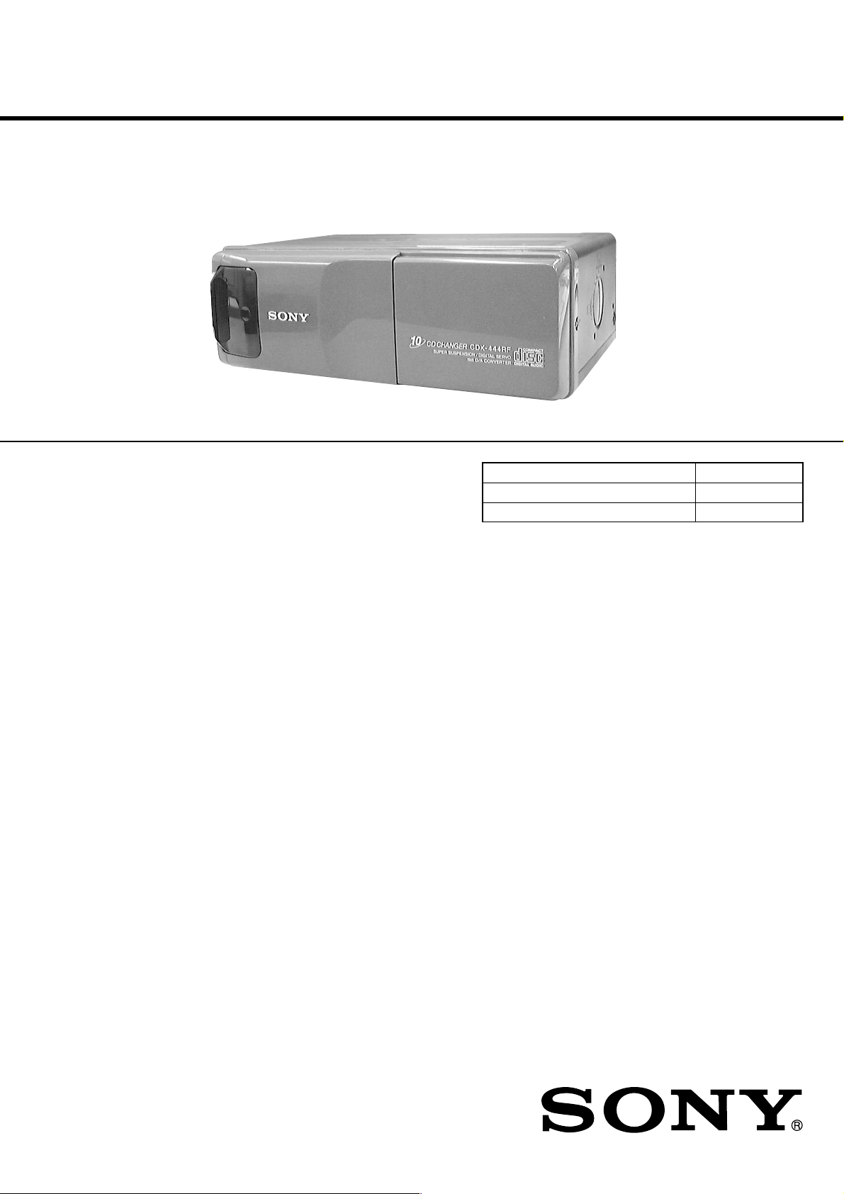
CDX-444RF
SERVICE MANUAL
Ver 1.1 2001.06
SPECIFICATIONS
US Model
Canadian Model
AEP Model
UK Model
E Model
Model Name Using Similar Mechanism CDX-434RF
CD Drive Mechanism Type MG-251A-137
Optical Pick-up Name KSS-720A
CD changer (CDX-444RF)
System Compact disc digital audio system
Laser Diode Properties
Material GaAlAs
Wavelength 780 nm
Emission Duration Continuous
Laser output power Less than 44.6 µW*
* This output is the value measured at a distance of 200 mm from the
objective lens surface on the Optical Pick-up Block.
Transmitting frequency 88.3 MHz/88.5 MHz/
88.7 MHz/88.9 MHz/
89.1 MHz/89.3 MHz/
89.5 MHz/89.7 MHz/
89.9 MHz (switchable)
Input/output terminals Wired remote control (8 pin)
RF signal (FM) output
Power input (3 pin)
Current drain 800 mA (at playback)
800 mA (at disc loading/ejecting)
Operating temperature –10°C to +55°C
(14°F to 131°F)
Dimensions Approx. 262 × 90 × 181.5 mm
(10 3/8 × 3 5/8 × 7 1/4 in.) (w/h/d)
Mass Approx. 2.1 kg (4 lb. 10 oz.)
Relay box
Input/output Antenna input terminal
Antenna output cord
CD Changer input cord
Dimensions Approx. 40 × 40 × 27 mm
(1 5/8 × 1 5/8 × 1 1/8 in.) (w/h/d)
Mass 140 g (5 oz.)
Wired remote (RM-X82RF)
Dimensions Approx. 122 × 36.5 × 15.5 mm
(4 7/8 × 1 7/16 × 5/8 in.) (w/h/d)
Mass Approx. 255 g (9 oz.)
Supplied accessories
Disc magazine (1)
Parts for installation and connections (1 set)
Design and specifications are subject to change without notice.
COMPACT DISC CHANGER SYSTEM
9-870-222-12 Sony Corporation
2001F0500-1 e Vehicle Company
C 2001.6 Shinagawa Tec Service Manual Production Group
Page 2
SERVICING NOTES
L
NOTES ON HANDLING THE OPTICAL PICKUP BLOCK OR BASE UNIT
The laser diode in the optical pick-up block may suffer electrostatic breakdown because of the potential difference generated by
the charged electrostatic load, etc. on clothing and the human body .
During repair, pay attention to electrostatic breakdown and also
use the procedure in the printed matter which is included in the
repair parts.
The flexible board is easily damaged and should be handled with
care.
NOTES ON LASER DIODE EMISSION CHECK
The laser beam on this model is concentrated so as to be focused
on the disc reflective surface by the objective lens in the optical
pick-up block. Therefore, when checking the laser diode emission, observe from more than 30 cm away from the objectiv e lens.
US/Canadian model:
If the optical pick-up block is defective, please replace the whole
optical pick-up block.
Never turn the semi-fixed resistor located at the side of optical
pick-up block.
OPTICA
PICK-UP
BLOCK
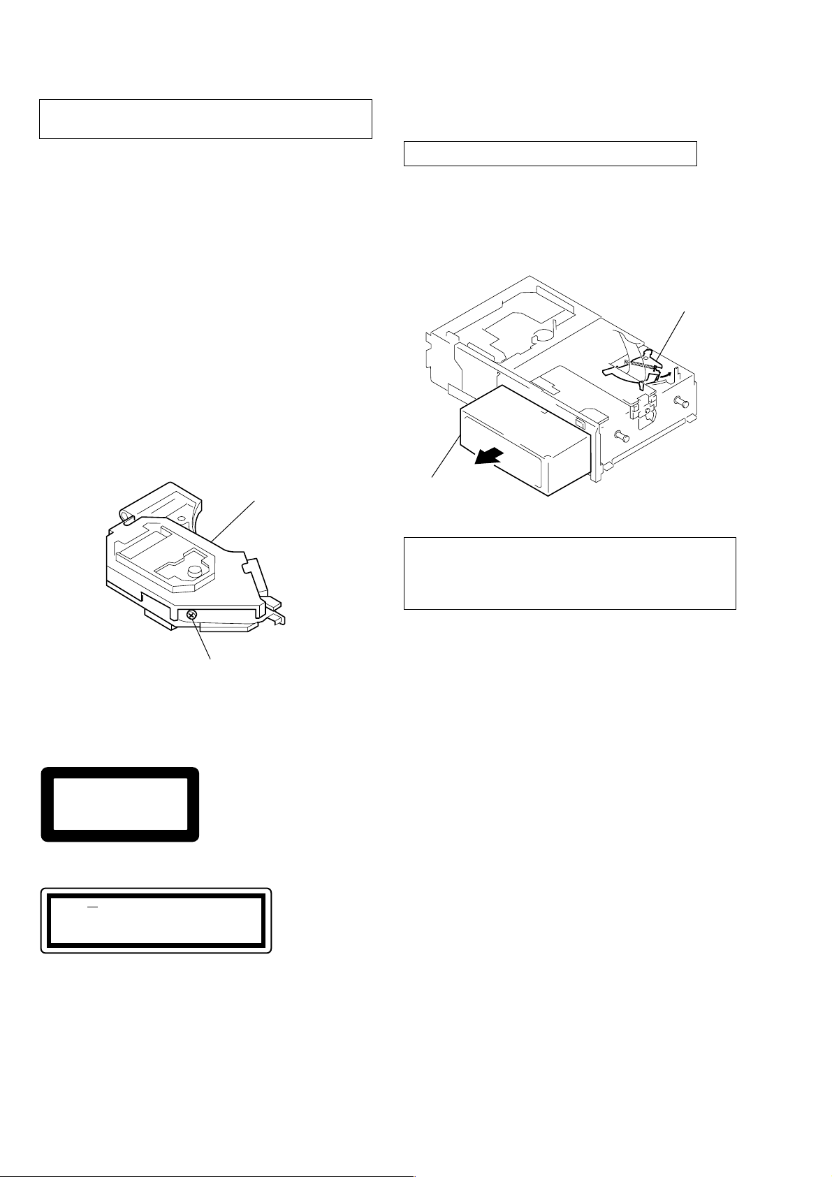
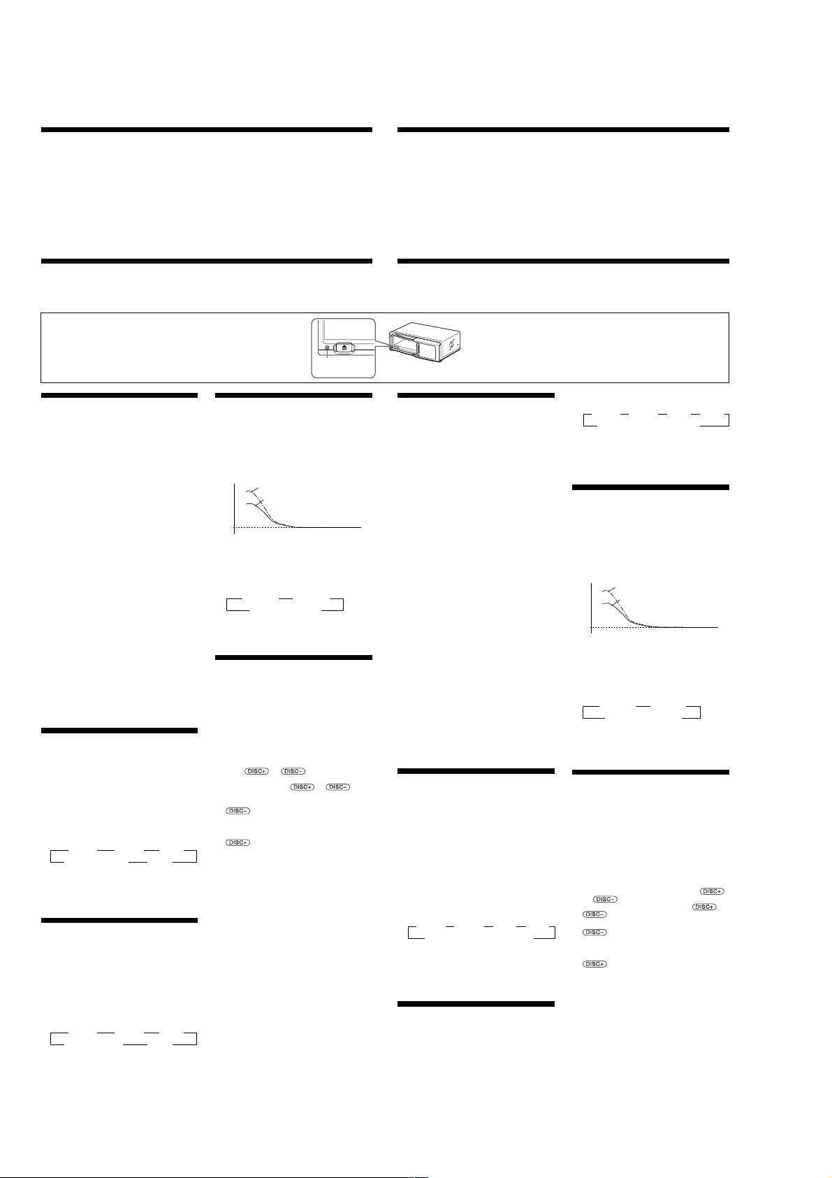
DISC MAGAZINE GETTING OUT PROCEDURE
ON THE POWER SUPPLY IS OFF
Remove the COVER (LOWER.T) ass’y beforehand
1) Press the lever (ML.S) to arrow direction.
2) Removal the magazine assy.
Note: Take out the magazine only when the tray is completely within the
magazine. If the disk or tray is sticking out, turn on the power and
eject the magazine.
Lever (ML.S)
Magazine assy
SEMI-FIXED
RESISTOR
AEP/UK model:
CLASS
1
PRODUCTLASER
The CLASS 1 LASER PRODUCT label is
located on the rear exterior.
CAUTION INVISIBLE
VIEW DIRECTLY WITH OPTICAL INSTRUMENTS
This label is located on the drive unit’s internal chassis.
When replacing the chassis (U.S) sub assy of mechanism deck
which have the “CAUTION LABEL” attached, please be sure to
put a new CA UTION LABEL (3-223-913-11) to the chassis (U.S)
sub assy.
LASER RADIATION WHEN OPEN
DO NOT STARE INTO BEAM OR
CAUTION
Use of controls or adjustments or performance of procedures
other than those specified herein may result in hazardous radiation exposure.
Notes on chip component replacement
• Never reuse a disconnected chip component.
• Notice that the minus side of a tantalum capacitor may be damaged by heat.
Flexible Circuit Board Repairing
• Keep the temperature of the soldering iron around 270 ˚C during repairing.
• Do not touch the soldering iron on the same conductor of the
circuit board (within 3 times).
• Be careful not to apply force on the conductor when soldering
or unsoldering.
SAFETY-RELATED COMPONENT WARNING!!
COMPONENTS IDENTIFIED BY MARK 0 OR DOTTED
LINE WITH MARK 0 ON THE SCHEMATIC DIAGRAMS
AND IN THE PARTS LIST ARE CRITICAL TO SAFE
OPERATION. REPLACE THESE COMPONENTS WITH
SONY PARTS WHOSE PART NUMBERS APPEAR AS
SHOWN IN THIS MANUAL OR IN SUPPLEMENTS PUBLISHED BY SONY.
ATTENTION AU COMPOSANT AYANT RAPPORT
À LA SÉCURITÉ!
LES COMPOSANTS IDENTIFIÉS P AR UNE MARQUE 0
SUR LES DIAGRAMMES SCHÉMATIQUES ET LA LISTE
DES PIÈCES SONT CRITIQUES POUR LA SÉCURITÉ
DE FONCTIONNEMENT. NE REMPLACER CES COMPOSANTS QUE PAR DES PIÈCES SONY DONT LES
NUMÉROS SONT DONNÉS DANS CE MANUEL OU
DANS LES SUPPLÉMENTS PUBLIÉS PAR SONY.
2
Page 3

TABLE OF CONTENTS
SERVICING NOTES .......................................................... 2
1. GENERAL
Location and Function of controls.................................. 4
Installation....................................................................... 8
Connections..................................................................... 9
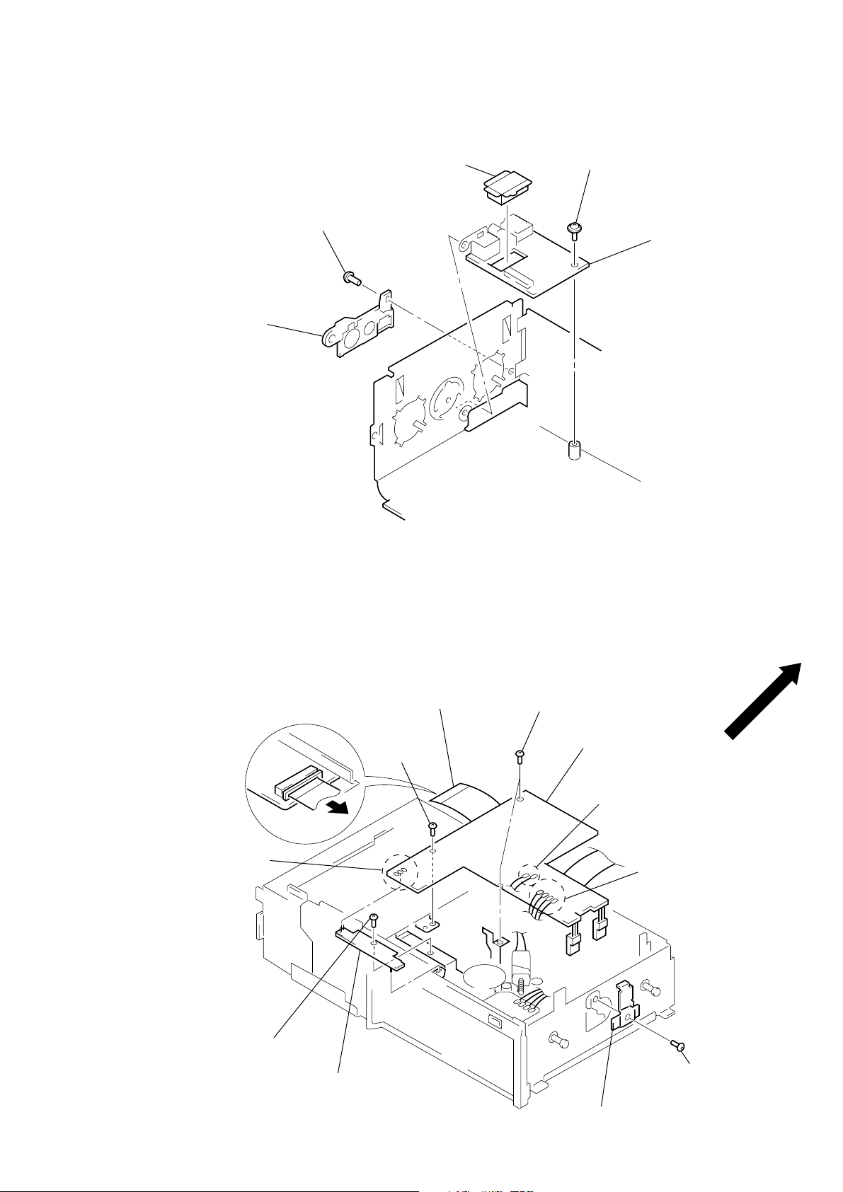
2. DISASSEMBLY ......................................................... 10
3. MECHANISM DECK ASSEMBLY ................... 16
4. MECHANICAL ADJUSTMENTS....................... 18
5. ELECTRICAL CHECK .......................................... 19
6. DIAGRAMS
6-1. Block Diagram – SERVO Section – .............................. 21
6-2. Block Diagram – MAIN Section – ................................ 22
6-3. Note for Printed Wiring Boards and
Schematic Diagrams ....................................................... 23
6-4. Printed Wiring Boards – RF/LSW Boards – ................. 24
6-5. Schematic Diagram – RF/LSW Boards –...................... 25
6-6. Printed Wiring Boards
– MAIN Board (Component Side) – .............................. 26
6-7. Printed Wiring Boards
– MAIN (Conductor Side)/SW Boards – ....................... 27
6-8. Schematic Diagram – MAIN Board (1/2) – .................. 28
6-9. Schematic Diagram – MAIN (2/2)/SW Boards – ......... 29
6-10. Printed Wiring Boards – FM Board –............................ 30
6-11. Schematic Diagram – FM Board – ................................. 31
6-12. IC Pin Function Description ........................................... 35
7. EXPLODED VIEWS................................................ 37
8. ELECTRICAL PARTS LIST ............................... 43
3
Page 4
SECTION 1
GENERAL
This section is extracted from
instruction manual.
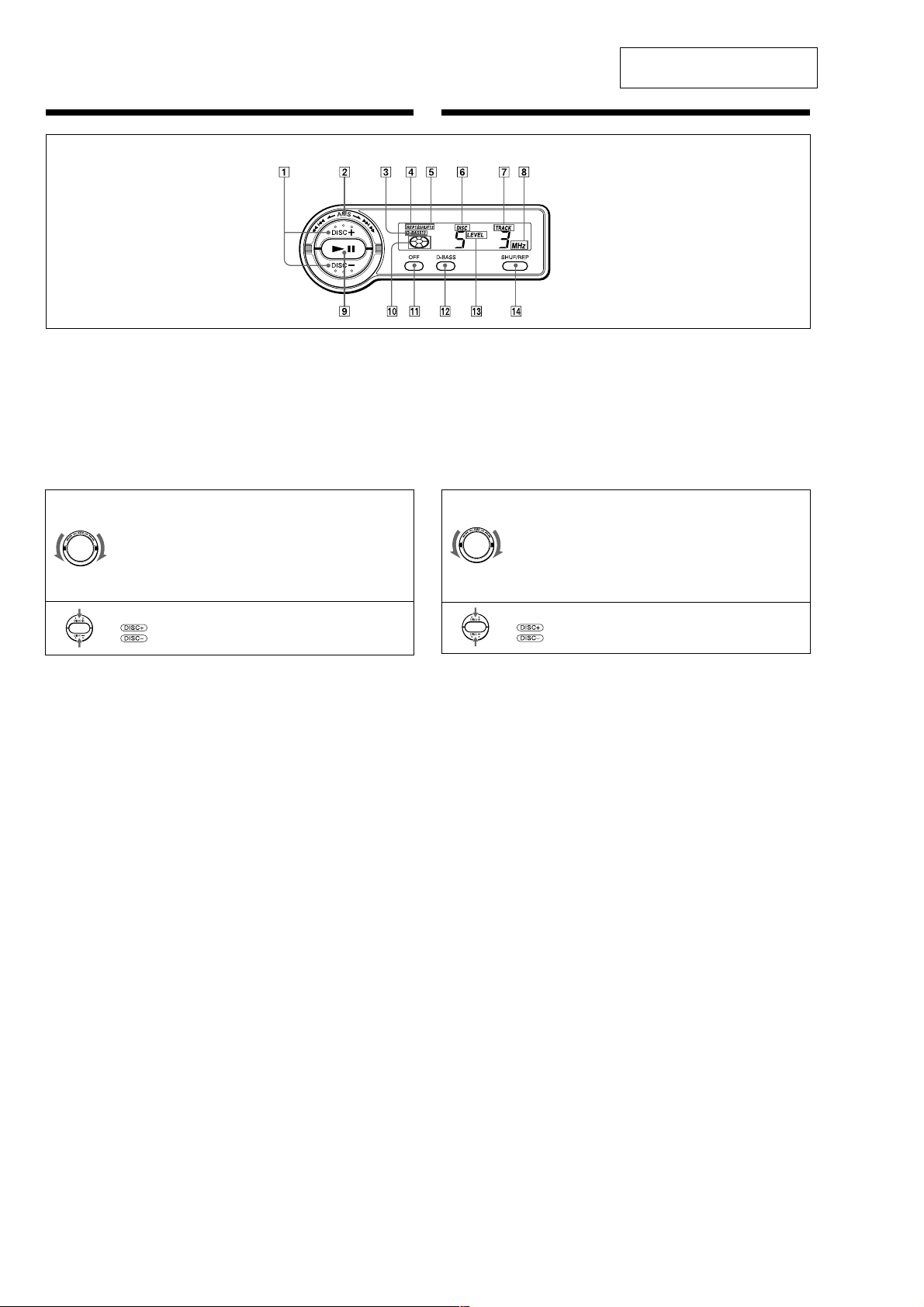
Location and function of controls
1 DISC (disc select) buttons
2 AMS (Automatic Music Sensor/manual
search) control
Depending on which side of the control you
push down, you can select from the following
functions.
3 D-BASS indication
4 REP (repeat play) indication
5 SHUF (shuffle play) indication
6 DISC (disc number) indication
The indicated disc number matches the disc
number in the disc magazine.
7 TRACK (track number) indication
AMS function
To locate the beginning of a track, push down
> to locate the beginning of the next track.
. to locate the beginning of the track currently played.
If you push down the control repeatedly, the beginnings of all following or
previous tracks will be located until the end of the disc is reached.
Manual search function
To quickly locate a desired point of a track, push down and hold
M to fast-forward.
m to fast-reverse.
The elapsed playing time of the track will be shown in the display window during
manual search.
Disc select function
To select a desired disc, press momentarily
to select the next disc.
to select the previous disc.
Nomenclature
Wired remote (RM-X82RF)/Télécommande à fil (RM-X82RF)
8 MHz (frequency) indication
9 u (play/pause) button
If pressed during CD playback, the CD will
pause. If pressed again, CD playback will
continue.
0 Play/pause indication
Turns around during CD playback and
flashes when the pause button is pressed.
qa OFF button
qs D-BASS button
qd LEVEL (output level) indication
qf SHUF/REP (shuffle play/repeat play/
control mode set) button
1 Touches DISC (sélection de disques)
2 Commande AMS (détecteur automatique de
musique/recherche manuelle)
Suivant le côté de la commande sur lequel vous
appuyez, vous pouvez sélectionner les
fonctions suivantes.
3 Indication D-BASS
4 Indication REP (répétition de la lecture)
5 Indication SHUF (lecture aléatoire)
6 Indication DISC (numéro de disque)
Le numéro de disque indiqué correspond au
numéro de disque dans le chargeur de disques.
7 Indication TRACK (numéro de plage)
8 Indication MHz (fréquence)
9 Touche u (lecture/pause)
Si vous appuyez sur cette touche en cours de
lecture CD, le CD passe en mode de pause. Si
vous appuyez de nouveau sur cette touche, la
lecture CD reprend.
0 Indication de lecture/pause
Tourne pendant la lecture d’un CD et clignote
lorsque la touche de pause est actionnée.
qa Touche OFF (arrêt de la lecture de CD)
qs Touche D-BASS
qd Indication LEVEL (niveau de sortie)
qf Touche SHUF/REP (lecture aléatoire/lecture
répétée/mode de réglage)
Fonction AMS
Pour localiser le début d’une plage, appuyez sur
> pour localiser le début de la plage suivante.
. pour localiser le début de la plage en cours.
Si vous appuyez plusieurs fois de suite sur la commande, le début de chacune des
plages précédentes ou des suivantes est localisé jusqu’à la fin du disque.
Fonction de recherche manuelle
Pour localiser rapidement un point désiré d’une plage, maintenez enfoncé
M pour avancer rapidement.
m pour reculer rapidement.
La durée écoulée de la plage apparaît sur l’afficheur pendant la recherche
manuelle.
Fonction de sélection de disques
Quand vous voulez sélectionner un disque, appuyez momentanément sur
pour choisir le disque suivant.
pour choisir le disque précédent.
4
Page 5
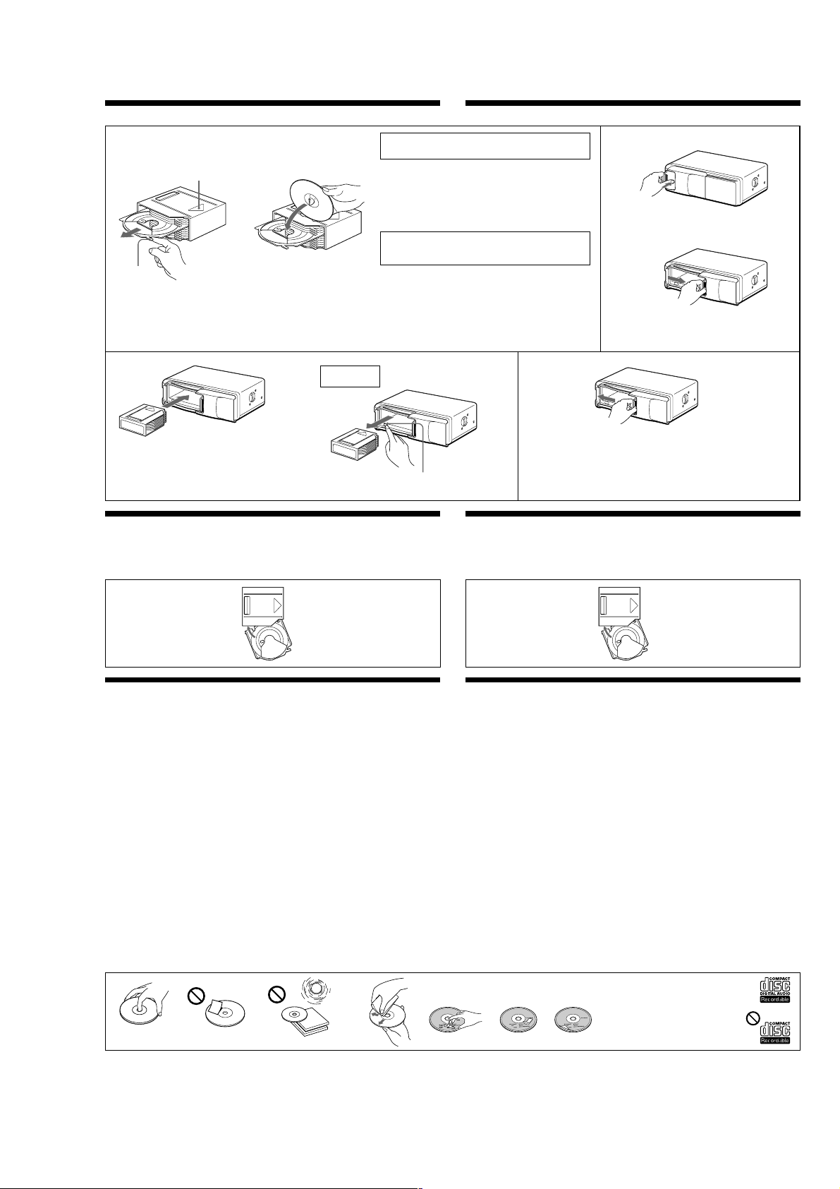
Inserting a disc Insertion d’un disque
1
With the arrow side facing up
Avec le côté portant la flèche orienté
vers le haut
Tab
Onglet
3
c
Labeled surface up
Face imprimée vers le haut
10 discs, one in each tray
10 disques, un par plateau
To remove
Retrait
Use the supplied disc magazine or the disc magazine XA-250. The
disc magazine XA-10B cannot be used with this unit. If you use any
other disc magazine, it may cause a malfunction.
Notes
• To listen to an 8 cm (3 in.) CD, use the optional Sony CD adaptor
CSA-8. Be sure to always use the specified adaptor, as failing to do so
may cause a malfunction of the unit. If you use any other adaptor, the
unit may not operate properly. When using the Sony CD adaptor,
make sure that the three catches on the adaptor are firmly latched
onto the 8 cm (3 in.) CD.
• Do not insert the Sony CD adaptor CSA-8 in the disc magazine without
a disc, malfunction may result.
Utilisez le magasin à disques fourni ou un magasin à disques XA-250.
Vous ne pouvez pas utiliser de magasin à disques XA-10B avec cet
appareil. L’utilisation d’un autre type de magasin à disques risque de
provoquer un dysfonctionnement.
Remarques
• Pour écouter un CD de 8 cm (3 po.) CD, utilisez l’adaptateur CD Sony
en option CSA-8. Veillez à toujours utiliser l’adaptateur spécifié, faute
de quoi vous risquez de provoquer un dysfonctionnement de
l’appareil. Si vous utilisez un autre adaptateur, l’appareil risque de ne
pas fonctionner correctement. Lorsque vous employez l’adaptateur CD
Sony, assurez-vous que les trois encoches de l’adaptateur soient
fermement engagées sur le CD de 8 cm (3 po.).
• N’introduisez pas l’adaptateur CD Sony CSA-8 dans le chargeur sans
disque, car il pourrait en résulter un dysfonctionnement.
4
Push to unlock the door
2
Poussez pour déverrouiller la porte
Slide open
Coulissez pour ouvrir
Note
To prevent injury, do not insert your hand in the CD changer.
Remarque
Pour éviter toute blessure, ne pas introduire la main dans le
changeur de CD.
x
Disc magazine
Chargeur de disques
If the disc magazine does not lock properly
Take out the disc magazine, press Z, and re-insert it.
Si vous ne pouvez pas fermer le chargeur de disques
Retirez le chargeur, appuyez sur Z et réintroduisez-le.
Z (EJECT)
Notes on the disc magazine
•Do not leave the disc magazine in locations with high temperature and high humidity, such as on a car
dashboard or in the rear window where the disc magazine will be subject to direct sunlight.
•Do not place more than one disc at a time onto a tray, otherwise the CD changer and the discs may be
damaged.
•Do not drop the disc magazine or subject it to a violent shock.
When the tray comes out
Normally, the trays will not come out of
the disc magazine. However, if they are
pulled out of the disc magazine, it is
easy to re-insert them.
With the cut-away portion of the
tray facing you, insert the right
corner of the tray in the slot, then
push in the left corner until it clicks.
Note
Do not insert the tray upside down or in
the wrong direction.
Notes on handling discs
A dirty or defective disc may cause sound drop-outs during playback. To enjoy optimum sound, handle
the disc as follows.
• Handle the disc by its edge, and do not touch the unlabled surface. (fig. A)
• Do not stick paper or tape on the disc. (fig. B)
• Keep your discs in their cases or disc magazines when not in use.
Do not expose the discs to direct sunlight or heat sources such as hot air-ducts. Do not leave the
discs in a car parked in direct sunlight where there can be a considerable rise in temperature
inside the car. (fig. C)
• Before playing, clean the discs with an optional cleaning cloth. Wipe each disc in the direction of
the arrows. (fig. D)
Do not use solvents such as benzine, thinner, commercially available cleaner, or antistatic spray intended
for analog discs.
• Discs with special shapes (heart-shaped discs, octagonal discs etc.) cannot be played on this unit.
Attempting to do so may damage the unit. Do not use such discs.
Notes on discs
If you use the discs explained below, the sticky residue can cause the disc to stop spinning and may cause
malfunction or ruin your discs.
Do not use second-hand or rental CDs that have a sticky residue on the surface (for example, from peeledoff stickers or from ink, or glue leaking from under the stickers).
• There are paste residue. Ink is sticky. (fig. E)
Do not use rental CDs with old labels that are beginning to peel off.
• Stickers that are beginning to peel away, leaving a sticky residue. (fig. F)
Do not use your discs with labels or stickers attached.
• Labels are attached. (fig. G)
Notes on CD-R discs
• You can play CD-Rs (recordable CDs) designed for audio use on this unit (fig. H).
• Some CD-Rs (depending on the equipment used for its recording or the condition of the disc) may
not play on this unit.
• You cannot play a CD-R that is not finalized*.
* A process necessary for a recorded CD-R disc to be played on the audio CD player.
Use the unit with the door closed completely
Otherwise, foreign matter may enter the unit and contaminate the lenses
inside the CD changer.
Utilisez cet appareil avec la fenêtre complètement fermée
Sinon, des corps étrangers risquent de pénétrer à l’intérieur de l’appareil et
d’encrasser les lentilles à l’intérieur du changeur de CD.
Remarques sur le chargeur de disques
•Ne pas laisser le chargeur de disques dans un endroit très chaud ou très humide comme sur le tableau
de bord ou sur la plage arrière d’une voiture où il serait en plein soleil.
•Ne placez pas plus d’un disque à la fois par plateau, faute de quoi vous risquez d’endommager le
changeur de CD et les disques.
•Ne pas laisser tomber le chargeur de disques ni le cogner.
Si un plateau s’enlève
En principe, les plateaux ne s’enlèvent
pas du magasin. S’ils s’enlèvent du
magasin, il est cependant facile de les y
réintroduire.
Remarques sur la manipulation des disques
Un disque sale ou défectueux peut provoquer des pertes de son à la lecture. Manipuler le disque comme
suit pour obtenir un son optimal.
• Saisissez les disques par les bords et n’en touchez jamais la surface. (fig. A)
• Ne collez pas de papier ni de bande adhésive sur le disque. (fig. B)
• Conservez vos disques dans leurs boîtiers ou des pochettes de rangement lorsqu’ils ne sont pas
utilisés.
N’exposez pas les disques au rayonnement direct du soleil ni à des sources de chaleur comme des
conduits d’air chaud. Ne laissez pas les disques dans une voiture parquée en plein soleil où la
température intérieure de l’habitable risque d’augmenter considérablement. (fig. C)
• Avant la lecture, essuyer les disques avec un chiffon de nettoyage optionnel. Essuyer chaque
disque dans le sens des flèches. (fig. D)
Ne pas utiliser de solvants tels que de la benzine, du diluant, des produits de nettoyage vendus dans le
commerce ou des vaporisateurs anti-statiques destinés aux disques analogiques.
• Il n’est pas possible d’utiliser les disques de formes spéciales (en forme de cœur ou octogonaux,
etc.) avec cet appareil. Vous risquez d’endommager l’appareil. N’essayez jamais de lire ces disques.
Remarques sur les disques
Si vous utilisez les disques décrits ci-dessous, le résidu adhésif risque de provoquer l’arrêt de la rotation
du disque et d’entraîner un dysfonctionnement ou d’endommager vos disques.
N’utilisez pas de CD de seconde main ou de location qui présentent des résidus adhésifs à la surface (par
exemple d’étiquettes décollées ou d’encre, de colle dépassant de l’étiquette).
• Résidus de colle. L’encre colle. (fig. E)
N’utilisez pas de CD de location avec d’anciennes étiquettes qui commencent à se décoller.
• Les étiquettes qui commencent à se décoller laissent des résidus adhésifs. (fig. F)
N’utilisez pas vos disques avec des étiquettes ou des autocollants apposés dessus.
• Les étiquettes sont fixées. (fig. G)
Remarques sur les disques CD-R
• Vous pouvez écouter avec cet appareil des CD-R (CD enregistrables) conçus pour une utilisation
audio. (fig. H)
• Certains CD-R (en fonction des conditions de l’équipement d’enregistrement ou du disque)
risquent de ne pas être lus avec cet appareil.
• Vous ne pouvez pas lire de disques CD-R non finalisés*.
* Un processus nécessaire à la lecture des disques CD-R enregistrés sur le lecteur de CD audio.
L’encoche du plateau étant face à
vous, introduisez l’angle droit du
plateau dans la fente et poussez
ensuite sur l’angle gauche jusqu’à ce
qu’il s’encliquette.
Remarque
N’introduisez pas le plateau à l’envers ni
dans le mauvais sens.
ABC D E FG
This way
Oui
Moisture condensation
On a rainy day or in a very damp area, moisture may condense on the lenses inside the unit, and the unit
will not operate properly. In such a case, remove the disc magazine and wait for about an hour until
the moisture has evaporated.
If you have any questions or problems concerning your unit that are not covered in this manual, please
consult your nearest Sony dealer.
Not this way
Non
Not this way
Non
This way
Oui
Remarque sur la condensation d’humidité
Les jours de pluie et dans les régions très humides, il se peut que de l’humidité se condense sur les
objectifs à l’intérieur de l’appareil, qui risque alors de ne pas fonctionner correctement. En pareil cas,
retirez le chargeur de disques et attendez environ une heure que l’humidité se soit complètement
évaporée.
Si vous avez des questions ou des problèmes au sujet de votre appareil qui ne sont pas abordés dans le
présent mode d’emploi, consultez votre revendeur Sony.
H
Look for this mark to distinguish CD-Rs
for audio use.
Ce symbole permet de distinguer les
CD-R conçus pour une utilisation audio.
This mark denotes that a disc is not for
audio use.
Ce symbole indique qu’un disque n’est
pas conçu pour une utilisation audio.
5
Page 6
Operation Fonctionnement
q
Precautions
•This unit cannot be used with a car audio without an FM tuner.
•If your car was parked in direct sunlight resulting in a considerable rise in temperature inside the car,
allow the unit to cool off before operating it.
•If no power is being supplied to the unit, check the connections first. If everything is in order, check the
fuse.
•Avoid installing the CD changer and wired remote in places:
— subject to temperature exceeding 55°C (131°F).
— subject to direct sunlight.
— near heat sources (such as heaters).
— exposed to rain or moisture.
— exposed to excessive dust or dirt.
— subject to excessive vibration.
Resetting the unit
Before operating the unit for the first time or after replacing the car battery, you must reset the unit. Press
the reset button with a pointed object, such as a ball-point pen, etc.
Reset button
Touche de
réinitialisation
Listening to a CD
1
Turn on the FM tuner of your car audio.
2
Tune in the selected transmitting
frequency* with the FM tuner of your car
audio.
* The frequency of the unit is set to 88.3 MHz at
the factory.
You can change the frequency. (See “Changing
the transmitting frequency” below.)
3
Press u.
CD playback starts.
4
Adjust the volume with the volume control
on your car audio.
All the tracks play from the beginning.
Stopping CD play
Press (OFF).
Notes
• When CD playback stops, you may hear some noise
from the speakers. To prevent this from happening,
turn the volume down before stopping CD playback.
• If you turn off the ignition switch of your car
without stopping CD playback, it will automatically
resume CD playback from where it was stopped
when you turn on the ignition switch again.
Listening to the radio or a tape
Be sure to stop CD playback before you start
listening to the radio or a tape.
Note
Be sure to stop CD playback, otherwise there may be
some interference with radio reception.
Playing tracks in random order
— Shuffle Play
You can select:
•SHUF 1–to play the tracks on the current disc in
random order.
•SHUF 2–to play all the discs in random order.
Press (SHUF/REP) repeatedly until the
desired setting appears (SHUF1 or SHUF2).
After five seconds, shuffle play starts.
Each time you press (SHUF/REP), the display
changes as follows:
B SHUF 1 B SHUF 2 B REP 1
Cancel (SHUF off) b REP 2 b
To go back to the normal playback mode, press
(SHUF/REP) repeatedly until the “SHUF” or
“REP” indication disappears.
Playing tracks repeatedly
— Repeat Play
You can select:
•REP 1–to repeat the track.
•REP 2–to repeat the disc.
Press (SHUF/REP) repeatedly until the
desired setting appears (REP1 or REP2).
After five seconds, the repeat play starts.
Each time you press (SHUF/REP), the display
changes as follows:
B SHUF 1 B SHUF 2 B REP 1
Cancel (REP off) b REP 2
To go back to the normal playback mode, press
(SHUF/REP) repeatedly until the “REP” or
“SHUF” indication disappears.
Boosting the bass sound
— D-bass
You can enjoy a powerful bass sound. The D-bass
function boosts the low frequency signal.
You can hear the bass line more clearly even while
the vocal volume remains the same. You can
emphasize and adjust the bass sound easily with
the D-BASS button.
D-BASS 2
Level
D-BASS 1
0dB
Frequency (Hz)
Adjusting the bass curve
Press (D-BASS) repeatedly to select the
desired bass curve.
As the D-BASS number increases so does the
effect.
B D-BASS 1 B D-BASS 2
Cancel (D-BASS off)b
Note
Setting the output level from 4 to 5, the amount of
bass boost decreases to avoid distortion.
Changing the transmitting frequency
Because this unit processes CD playback sound
through an FM tuner, there may be interference
noise during CD playback. In such a case, change
the frequency of the modulated RF signal
transmitted from the unit. The initial setting is
88.3 MHz.
1
Press (SHUF/REP) for two seconds until
frequency appears.
2
Press
select the frequency.
Each time you press
frequencys changes as follows:
3
Press (SHUF/REP) for two seconds.
Notes
• When you change the transmitting frequency on the
unit, be sure to tune your FM tuner to the newly
selected one.
• Press u on the wired remote before changing the
frequency if the power to the unit is turned off.
or repeatedly to
or , the
: 88.3 MHz t 89.9 MHz t 89.7 MHz
t 89.5 MHz t 89.3 MHz t 89.1
MHz t 88.9 MHz t 88.7 MHz t
88.5 MHz t 88.3 MHz
: 88.3 MHz t 88.5 MHz t 88.7 MHz
t 88.9 MHz t 89.1 MHz t
89.3 MHz t 89.5 MHz t 89.7 MHz
t 89.9 MHz t 88.3 MHz
Précautions
•Cet appareil ne peut être utilisé avec un autoradio sans syntoniseur FM.
•Si votre voiture est parquée en plein soleil, provoquant ainsi une augmentation considérable de la
température dans l’habitacle, laissez l’appareil refroidir avant de l’utiliser.
•Si l’appareil n’est pas alimenté, vérifiez d’abord les connexions. Si tout est en ordre, contrôlez le fusible.
•Evitez d’installer le changeur de CD et la télécommande à fil à un endroit :
— où la température peut dépasser 55°C (131°F),
— en plein soleil,
— près d’une source de chaleur (comme un chauffage),
— exposé à la pluie ou à l’humidité,
— poussiéreux ou sale,
— exposé à des vibrations fortes.
Réinitialisation de l’appareil
Avant la première mise en service de cet appareil ou après avoir remplacé la batterie de la voiture, vous
devez réinitialiser l’appareil.
Appuyez sur la touche de réinitialisation à l’aide d’un objet pointu comme un stylo à bille, etc.
A chaque pression sur (SHUF/REP), l’affichage
Lecture d’un CD
1
Mettez sous tension le syntoniseur FM de
votre autoradio.
2
Syntonisez la fréquence de transmission*
sélectionnée avec le syntoniseur FM de
votre autoradio.
* La fréquence de l ’appareil est réglée par défaut
sur 88,3 MHz.
Vous pouvez changer la fréquence. (Voir
“Changement de la fréquence de
transmission” ci-dessous.)
3
Appuyez sur u.
La lecture du CD démarre.
4
Réglez le volume à l’aide de la commande
du volume de votre autoradio.
Toutes les plages sont reproduites à partir du
début.
Pour arrêter la lecture d’un CD
Appuyez sur (OFF).
Remarques
• Lorsque vous arrêtez la lecture d’un CD, il se peut
que vous entendiez des parasites dans les hautparleurs. Pour éviter ce phénomène, baissez le
volume avant d’arrêter la lecture du CD.
• Si vous coupez le contact de votre voiture sans
arrêter la lecture du CD, celle-ci reprendra
automatiquement là où elle a été interrompue
lorsque vous remettrez le contact.
Ecouter la radio ou une cassette
Arrêtez la lecture du CD avant d’écouter la radio
ou une cassette.
Remarque
Si vous n’arrêtez pas la lecture du CD, des
interférences risquent de se produire avec la réception
radio.
Lecture des plages dans un ordre
quelconque
— Lecture aléatoire
Vous pouvez sélectionner:
•SHUF 1–pour reproduire les plages du disque
en place dans un ordre quelconque.
•SHUF 2–pour reproduire tous les disques dans
un ordre quelconque.
Appuyez plusieurs fois sur (SHUF/REP)
jusqu’à ce que le réglage souhaité
apparaisse (SHUF1 ou SHUF2).
La lecture aléatoire commence dans les cinq
secondes qui suivent.
A chaque pression sur (SHUF/REP), l’affichage
change de la façon suivante:
B SHUF 1 B SHUF 2 B REP 1 B REP 2
Annulation (SHUF hors service) b
Pour revenir à la lecture normale, appuyez
plusieurs fois de suite sur (SHUF/REP) jusqu’à
ce que l’indication “SHUF” ou “REP”
disparaisse.
Répétition de plages
— Lecture répétée
Vous pouvez sélectionner:
•REP 1–pour répéter une plage.
•REP 2–pour répéter tout un disque.
Appuyez plusieurs fois sur (SHUF/REP)
jusqu’à ce que le réglage souhaité
apparaisse (REP1 ou REP2).
La lecture répétée commence dans les cinq
ui suivent.
secondes
change de la façon suivante:
B SHUF 1 B SHUF 2 B REP 1 B REP 2
Annulation (REP hors service) b
Pour revenir à la lecture normale, appuyez
plusieurs fois de suite sur (SHUF/REP) jusqu’à
ce que l’indication “REP” ou “SHUF”
disparaisse.
Renforcement des graves
— D-bass
Vous pouvez exploiter des graves puissantes. La
fonction D-bass renforce les signaux de basse
fréquence.
Vous entendez plus distinctement les graves,
même si le volume de la partie vocale reste au
même niveau. Vous pouvez renforcer et ajuster
les graves à l’aide de la touche D-BASS.
D-BASS 2
D-BASS 1
Niveau
0dB
Fréquence (Hz)
Réglage de la courbe des graves
Appuyez plusieurs fois de suite sur
(D-BASS) pour sélectionner la courbe des
graves voulue.
L’effet s’intensifie à mesure que la valeur DBASS augmente.
B D-BASS 1 B D-BASS 2
Annuler (D-BASS off) b
Remarque
En modifiant le niveau de sortie de 4 à 5, le degré
d’accentuation du grave diminue afin d’éliminer toute
distcasion.
Changement de la fréquence de
transmission
Comme cet appareil traite le son de lecture CD via
un syntoniseur FM, il se peut qu’il y ait des
interférences durant la lecture du CD. En pareil
cas, changez la fréquence du signal RF modulé
transmis par l’appareil. Le réglage initial est de
88,3 MHz.
1
Appuyez sur (SHUF/REP) pendant deux
secondes jusqu’à ce que la fréquence
apparaisse.
2
Appuyez plusieurs fois de suite sur
ou pour sélectionner la fréquence.
Chaque fois que vous appuyez sur
, la fréquence change dans l’ordre
suivant :
: 88.3 MHz t 89.9 MHz t 89.7 MHz
t 89.5 MHz t 89.3 MHz t 89.1
MHz t 88.9 MHz t 88.7 MHz t
88.5 MHz t 88.3 MHz
: 88.3 MHz t 88.5 MHz t 88.7 MHz
t 88.9 MHz t 89.1 MHz t
89.3 MHz t 89.5 MHz t 89.7 MHz
t 89.9 MHz t 88.3 MHz
3
Appuyez sur (SHUF/REP) pendant deux
secondes.
Remarques
• Si vous changez la fréquence de transmission de
l’appareil, n’oubliez pas de syntoniser votre
syntoniseur FM sur la nouvelle fréquence
sélectionnée.
• Appuyez sur la touche u de la télécommande
filaire avant de changer la fréquence si l’appareil
n’est pas sous tension.
ou
6
Page 7

Changing the output level
You can select the output level from the unit.
Normally the unit is used at the initial output
level; change the level if necessary.
1
Press (SHUF/REP) for two seconds.
2
Press (SHUF/REP) momentarily.
Initial setting
3
Press
the output level.
To decrease the output level
To increase the output level
4
Press (SHUF/REP) for two seconds.
Note
When you select level 4 or 5, the CD playback sound
may be distorted or you may hear some noise. In such a
case, select a lower output level on the unit and turn
down the overall volume on your car audio.
or repeatedly to select
: ,
: ,
Changement du niveau de sortie
Vous pouvez sélectionner le niveau de sortie de
l’appareil. En principe, l’appareil est utilisé au
niveau de sortie initial ; changez le niveau si
nécessaire.
1
Appuyez sur (SHUF/REP) pendant deux
secondes.
2
Appuyez brièvement sur (SHUF/REP).
Réglage initial
3
Appuyez plusieurs fois de suite sur
ou pour sélectionner le niveau de
sortie.
Pour diminuer le niveau de sortie
: ,
Pour augmenter le niveau de sortie
: ,
4
Appuyez sur (SHUF/REP) pendant deux
secondes.
Remarque
Si vous sélectionnez le niveau 4 ou 5, le son de lecture
CD peut comporter des distorsions ou des parasites. En
pareil cas, sélectionnez un niveau de sortie inférieure
et baissez le volume de votre autoradio.
7
Page 8
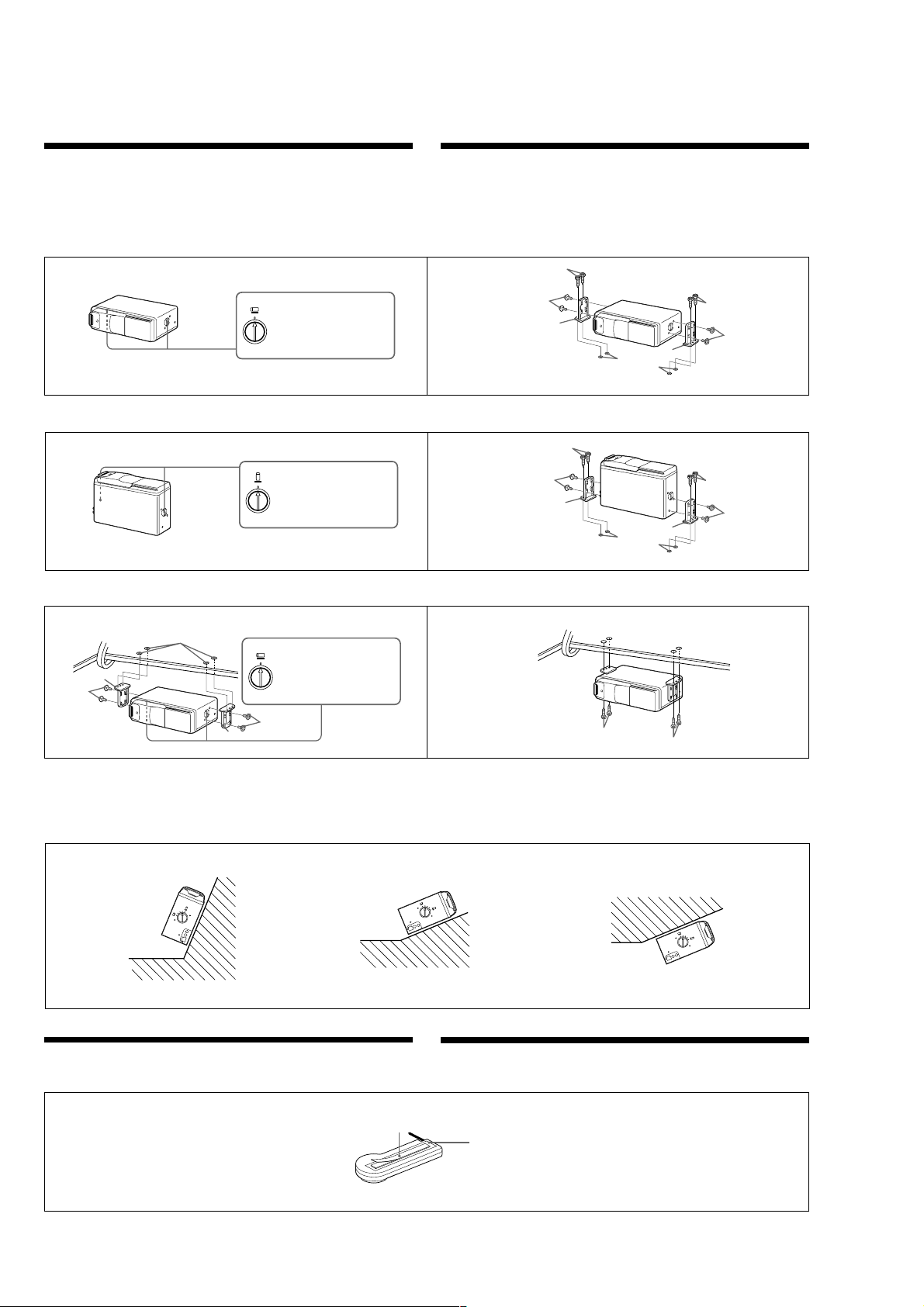
Installation
Installation
How to install the CD changer
•When you install the CD changer, be careful not to damage wiring or equipment on the other side of the
mounting surface.
•The brackets 1 provide two positions for mounting, high and low. Use the appropriate screw holes
according to your preference.
Installation du changeur de CD
•Quand vous installez le changeur de CD, veillez à ne pas endommager les câbles ou les instruments qui
se trouvent de l’autre côté.
•Les supports 1 offrent deux positions de montage, haut et bas. Utilisez les trous de vissage appropriés
en fonction de vos préférences.
Horizontal installation Installation horizontale
1
Vertical installation
1
Suspended installation
HORIZONTAL
Align with the marked position.
Alignez sur le repère.
VERTICAL
Align with the marked position.
Alignez sur le repère.
2
Installation verticale
2
Installation suspendue
3
2
1
ø 3.5 mm
5
(
/
32
in.)
ø 3,5 mm
5
(
/
32
po.)
3
2
1
3
2
1
ø 3.5 mm
5
/
32
in.)
(
ø 3,5 mm
5
/
32
po.)
(
3
2
1
5
ø 3.5 mm (
/
32
in.)
1
1
ø 3,5 mm (
5
/
32
po.)
HORIZONTAL
Align with the marked position.
Alignez sur le repère.
2
2
2
1
When the unit is to be installed under the rear tray or in the trunk, observe the following.
•Choose the mounting location carefully so the unit can be installed horizontally.
•Make sure the unit does not hinder the action of the torsion bar spring, hinge, etc. of the deck lid.
Si vous comptez installer le changeur de CD sous la plage arrière ou dans le coffre, prenez les précautions
suivantes.
•Choisissez soigneusement l’emplacement pour que le changeur soit à l’horizontale.
•Assurez-vous que l’appareil n’entrave pas l’action du ressort à barre de torsion, des charnières, etc., du
couvercle de la malle.
Inclined installation Installation inclinée
After installing the unit, align the dials with one of the marks so the arrow comes as close to a
vertical position as possible.
V
E
R
T
I
C
A
L
ONTAL
IZ
HOR
Note
Be sure to align the left and right dials with the same mark.
Installing the wired remote
Use the supplied double-sided adhesive tape 4, and mount the wired remote in a suitable location where
it will not interfere with your driving.
Après avoir installé l’appareil, alignez les disques sur l’un des repères afin que la flèche soit aussi
proche que possible de la position verticale.
L
A
T
N
O
IZ
R
V
O
H
E
R
T
IC
A
L
Remarque
Veillez à aligner les disques gauche et droite sur le même repère.
Installation de la télécommande à fil
Utilisez la bande à double face adhésive fournie 4 pour installer la télécommande à fil dans un endroit
qui ne risque pas de gêner la conduite.
3
3
L
A
T
N
O
Z
I
R
VERTICAL
O
H
4
The back of the wired remote
Dos de la télécommande à fil
8
Page 9
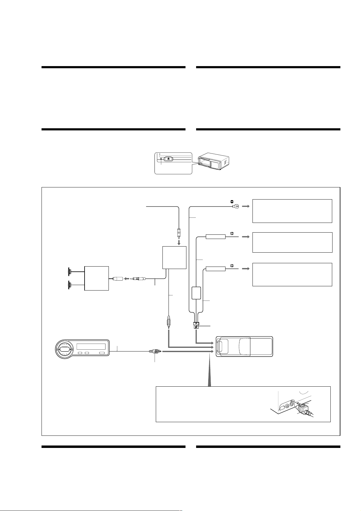
Connections
Connexions
Caution
•This unit is designed for negative ground 12 V
DC operation only.
•Before making connections, turn the car ignition
off to avoid short circuits.
•Connect the yellow and red power input leads
only after all other leads have been connected.
•Be sure to connect the red power input lead
to the positive 12 V power terminal which is
powered when the ignition switch is in the
accessory position.
•Run all ground wires to a common earth
point.
•When finished making all the connections,
press the reset button of the CD changer.
(See “Reset button” below.)
•The use of optical instruments with this
product will increase eye hazard.
Reset button
After the installation and connections are completed or the batteries have been changed, be sure to press
the reset button with a ball-point pen, etc.
Reset button
Touche de réinitialisation
Précautions
•Cet appareil est uniquement conçu pour
fonctionner sur 12 V CC avec une masse
négative.
•Avant d’effectuer les raccordements, coupez le
contact du véhicule pour éviter tout court-circuit.
•Branchez les fils d‘entrée d‘alimentation jaune et
rouge seulement après avoir terminé tous les
autres branchements.
Touche de réinitialisation
Après avoir terminé l’installation et les connexions ou remplacé les piles, appuyez sur la touche de
réinitialisation du changeur de CD à l’aide d’un stylo à bille, etc.
Connection diagram Schéma de connexion
Speaker system
Système de
haut-parleurs
* An adaptor (optional) may be necessary for your
car and car audio system. In such a case, consult
your dealer.
* Un adaptateur (en option) peut s’avérer nécessaire
suivant votre voiture et votre autoradio. En pareil
cas, consultez votre revendeur.
Car audio
Autoradio
from the car antenna*
depuis l’antenne de la voiture*
Antenna connector*
Connecteur d‘antenne*
0.5 m
0,5 m
Relay box
Boîtier de relais
6
5 m
1 m
Fuse
Fusible
5 m
Fuse
Fusible
5 m
5
Black
Noir
Yellow
Jaune
Red
Rouge
•Veillez à ne pas raccorder le fil rouge d‘entrée
d‘alimentation à la borne positive de 12 V qui est
alimentée quand la clé de contact est sur la
position accessoire.
•Rassemblez tous les fils de terre en un point
de masse commun.
•Lorsque vous avez terminé toutes les
connexions, appuyez sur la touche de
réinitialisation du changeur de CD. (Voir
“Touche de réinitialisation” ci-dessous.)
•L’utilisation d’instruments optiques avec ce
produit augmente les risques pour les yeux.
to a metal point on the car
First connect the black earth lead, then connect the yellow
and red power input leads.
vers un point métallique de la voiture
Branchez d’abord le fil de masse noir et, ensuite, les fils
d’entrée d’alimentation jaune et rouge.
to the +12 V power terminal which is powered at all times
Be sure to connect the black earth lead first.
à la borne d’alimentation +12 V qui est alimentée en
permanence
Raccordez d’abord le fil de masse noir.
to the +12 V power terminal which is powered when the
ignition switch is in the accessory position
Be sure to connect the black earth lead first.
à la borne d’alimentation de +12 V qui est alimentée quand
la clé de contact est sur la position accessoire
Raccordez d’abord le fil de masse noir.
Wired Remote
Télécommande à fil
Fuse replacement
If the fuse blows, check the power connection and
replace the fuse. If the fuse blows again after
replacement, there may be an internal malfunction.
5.5 m
5,5 m
Insert the connector until it locks.
Insérez le connecteur jusqu’à ce
qu’il s’enclenche.
WARNING
Plug the connector into the jack
on the left side of the CD changer.
Make sure that the catch of the
connector is secured in the hole
next to the jack.
Warning
Use a fuse with the specified amperage rating.
Use of a higher amperage fuse may cause serious
damage.
CD changer
Changeur de CD
AVERTISSEMENT
Branchez le connecteur sur la
prise du côté gauche du changeur
de CD. Assurez-vous que l’ergot
du connecteur s’adapte dans
l’orifice à côté de la prise.
Remplacement du fusible
Si le fusible saute, vérifiez la connexion
d’alimentation et remplacez-le. Si le fusible saute à
nouveau quand vous venez de le remplacer, il
s’agit peut être d’un mauvais fonctionnement
interne.
Catch
Ergot
Connector
Connecteur
Avertissement
Utilisez un fusible de l’ampérage spécifié.
L’utilisation d’un fusible d’ampérage supérieur
peut causer de sérieux dommages.
9
Page 10
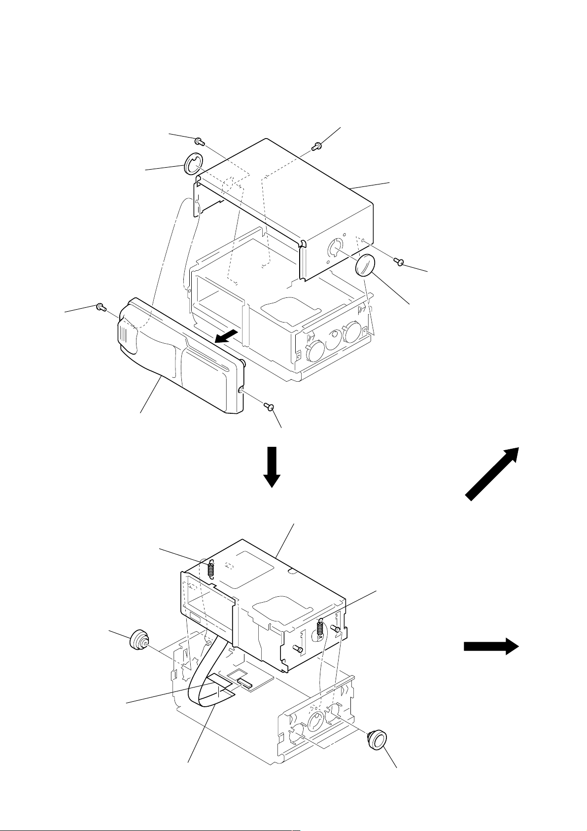
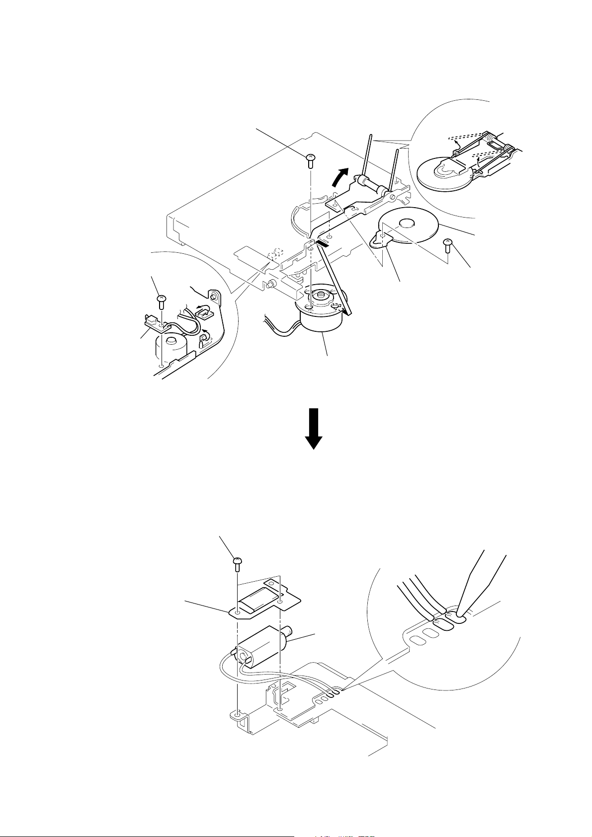
SECTION 2
)
)
DISASSEMBLY
Note: Follow the disassembly procedure in the numerical order given.
CASE (UPPER. T), FRONT PANEL ASSY
3
1
screw
(PTT2.6
screw
(PTT2.6
4
lever (FLT)
×
6)
×
6)
3
screw (PTT2.6 × 6)
5
case (upper. T)
4
lever (FLT)
3
screw (PTT2.6 × 6
2
front panel assy
MECHANISM DECK (MG-251A-137)
2
tension coil spring (FL)
1
two dampers (T)
1
screw (PTT2.6 × 6)
4
mechanism deck
(MG-251A-137)
2
tension coil spring (FL
10
filament tape
3
FM flexible board
(CN701)
1
two dampers (T)
Page 11
d
FM BOARD
3
cover
(FM connector.T)
1
screw
(BVTT2.6
2
4
cover (FM)
×
6)
screw
(ground)
5
FM boar
MAIN BOARD, SLIDE VARIABLE RESISTOR (ELEVATOR HEIGHT SENSOR) (RV202)
1 main flexible board
(CNJ101)
6 screw
(PTT2 × 4)
2 Remove three solders
of the slide variable resistor
(RV202).
8 screw
(PTT2 × 4)
9 slide variable resistor
(elevator height sensor)
(RV202)
5 two screws (FP)
7 main board
2 Remove two solders of
the elevator motor leads (M104).
2 Remove four solders of
the SW board leads.
4 heat sink (T)
3 screw (PTT2 × 4)
11
Page 12
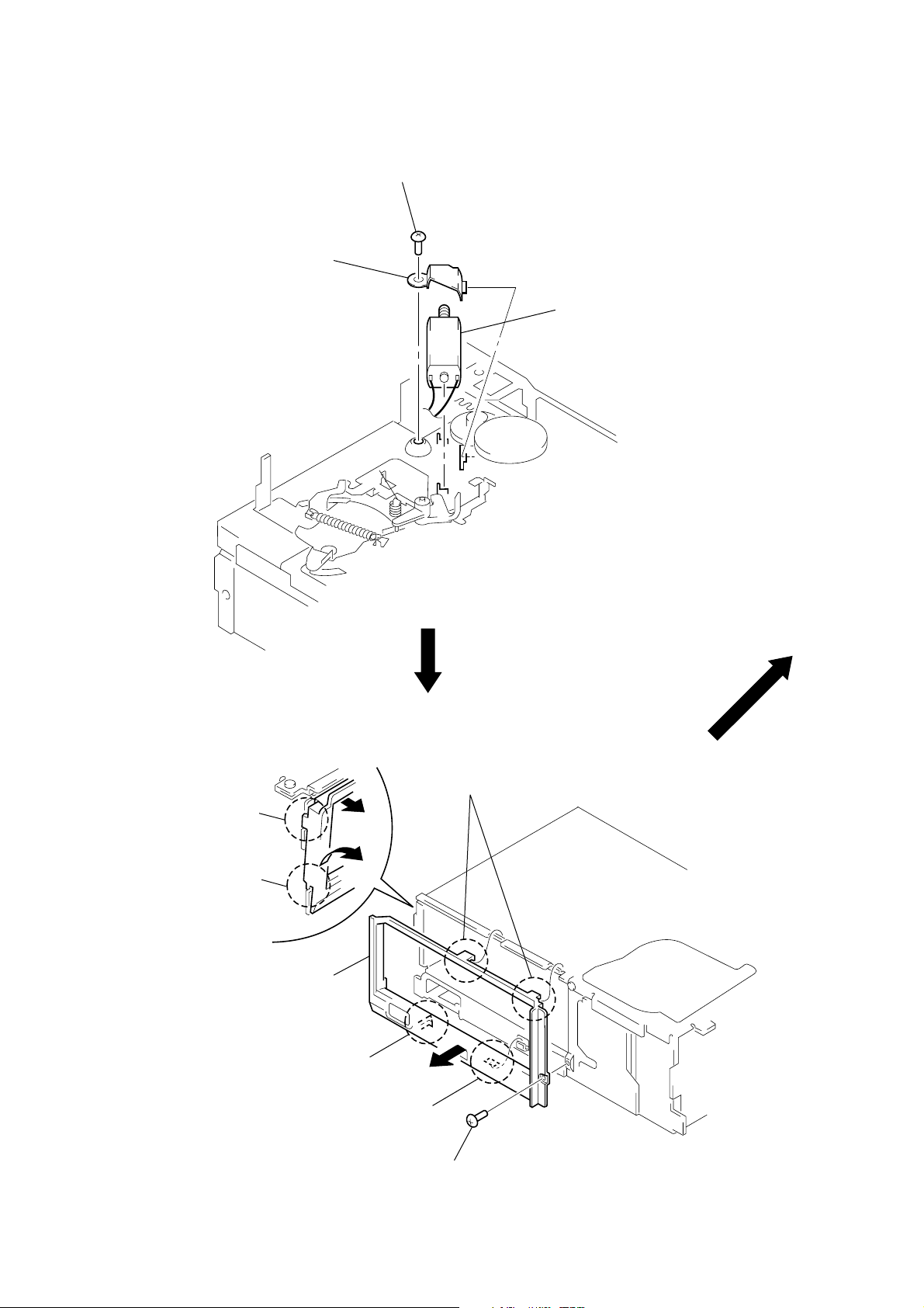
ELJ MOTOR ASSY (ELEVATOR) (M104)
2
bracket (EVM.S)
1
screw
(PTT2
×
4)
3
ELJ motor assy (elevator)
(M104)
ESCUTCHEON (T)
2
Remove the claw
in the direction of arrow
4
Remove the ditch
in the direction of arrow
5
A
.
B
.
Remove the escutcheon (T)
in the direction of arrow
C
two claws
3
A
B
.
3
claw
C
4
ditch
1
screw (T)
12
Page 13
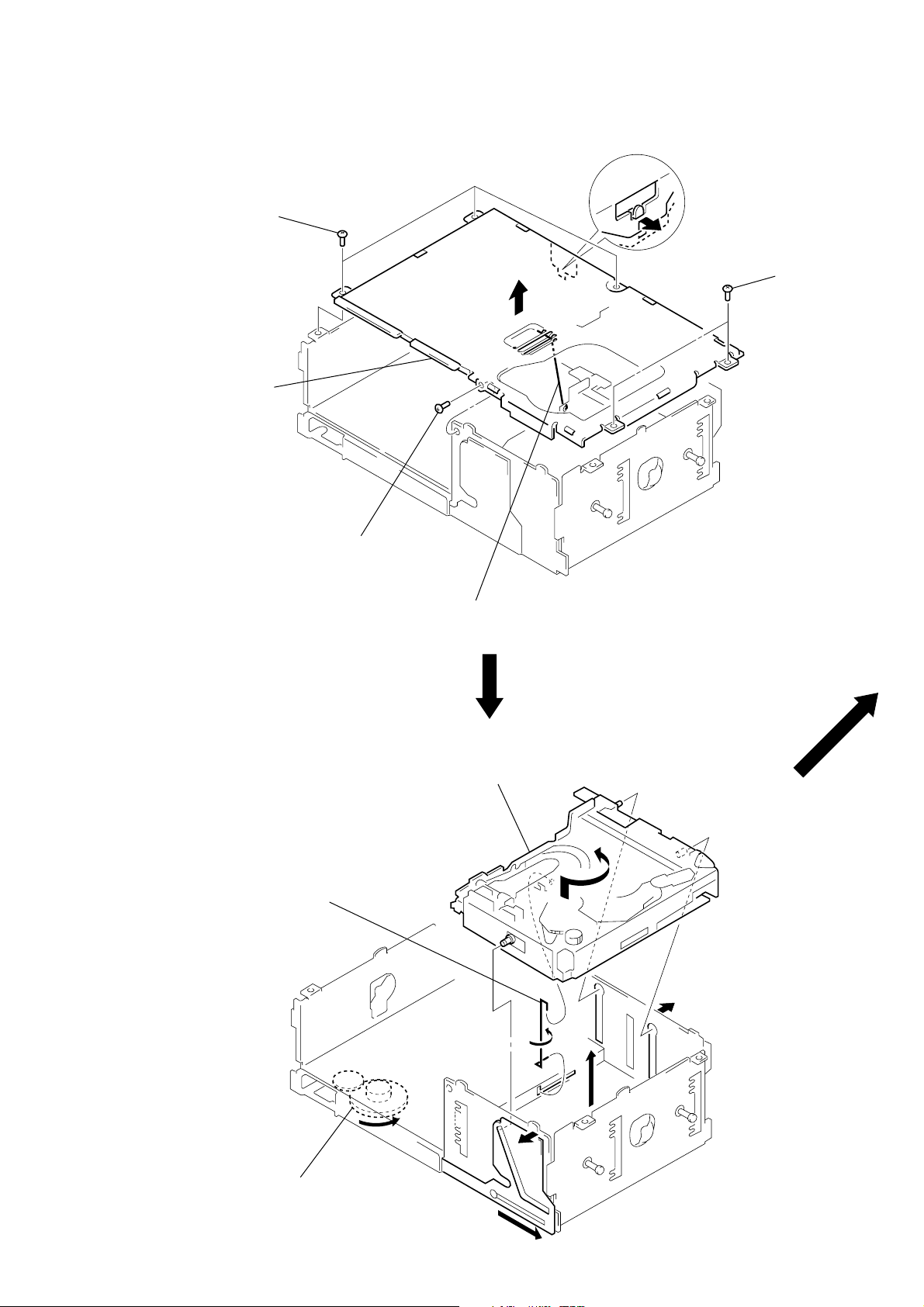
CHASSIS (U.S) SUB ASSY
1
three screws
(PTT2
×
4)
5
chassis (U.S) sub assy
1
screw
(PTT2 × 4)
3
A
2
Remove the edge
in the direction
of arrow A.
1
two screws
(PTT2 × 4)
CHASSIS ASSY
5
spring (stopper.lower)
4
spring (SUT)
6
chassis assy
4
3
1
Turn the gear (EVD.S) fully
in the direction of arrow A.
2
A
3
13
Page 14
RF BOARD
3
two screws
(PS2
×
4)
4
RF board
3
two screws
×
4)
(PS2
2
Remove four solders
of the LSW board leads
and spindle motor leads (M102).
2
Remove two solders
of the sled motor leads
(M101).
1
OP flexible board (CN102).
SLED MOTOR ASSY (251) (M101), OPTICAL PICK-UP (KSS-720A)
1
two precision screws
(P2
×
4
Turn shaft (feed) assy
in the direction
of the arrow,
then remove it.
3)
2
sled motor assy (251)
(M101)
OP flexible board
adhesive
sheet
14
3
optical pick-up
(KSS-720A)
optical
pick-up
Note: After connecting OP flexible board,
fix it with adhesive sheet
to optical pick-up.
Page 15
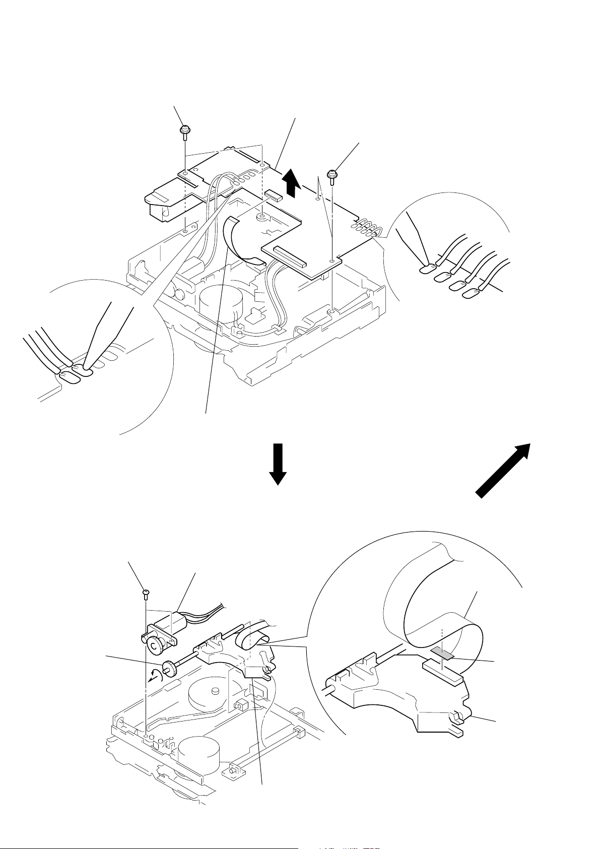
LSW BOARD, SPINDLE MOTOR (S) SUB ASSY (M102)
)
w
8
two precision screws
(P1.7
×
2.2)
1
precision screw
(P2
×
2.5)
2
LSW board
9
7
spring (chucking)
3
6
retainer (disc
4
precision scre
5
bracket (CP)
Remove the spindle motor (S) sub assy (M102)
in the direction of the arrow.
(P2 × 2.2)
ELJ MOTOR ASSY (CHUCKING) (M103)
2
two screws
(PTT2 × 4)
3
retainer (CHM)
4
ELJ motor
assy
(chucking)
(M103)
1
Remove two solders of
the chucking motor leads (M103).
15
Page 16
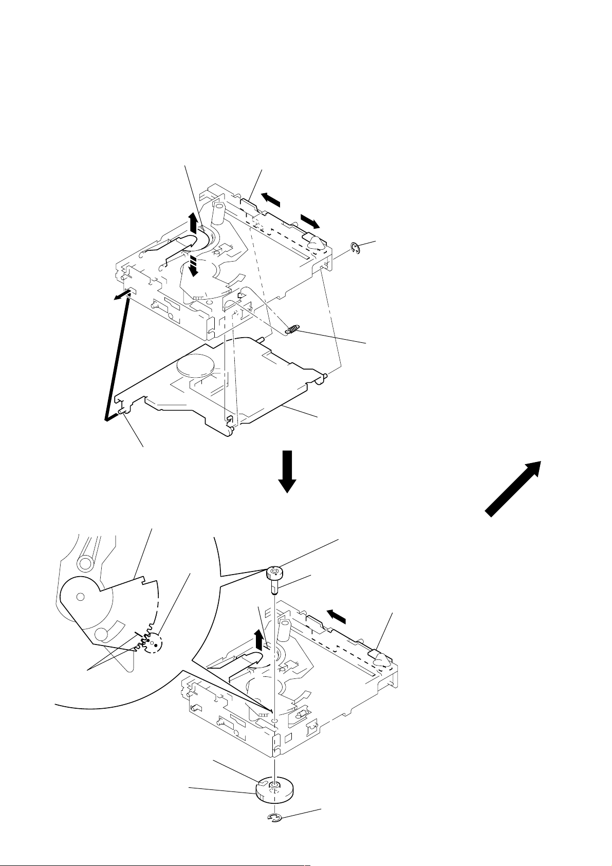
SECTION 3
)
MECHANISM DECK ASSEMBLY
Note: Follow the assembly procedure in the numerical order given.
OPTICAL PICK-UP COMPLETE ASSY
1
Move the lever (LOCK 3A) in the direction of arrow A,
and return it a little in the direction of arrow B
chuck plate
from the position where the chuck plate is moved
down to the lower limit.
B
A
3
stop ring 2.0 (E type
shaft (A)
GEAR (LOMINI)/(LOAD CAM) ASSY
gear (LOAD 2)
gear (LOMINI)
chuck plate
4
tension spring (DH)
2
optical pick-up complete assy
Note: Insert the shaft (A) first.
2
Attach the gear (LOMINI) at the position
shown in Fig. A.
shaft (rotary prevention C)
1
B
Move the lever (LOCK 3A)
fully in the direction of arrow
to move the chuck plate up.
B
16
marking
Fig. A
3
Attach the gear (LOAD CAM) assy
with its facing inside.
slit
stop ring 1.5 (E type)
4
Page 17
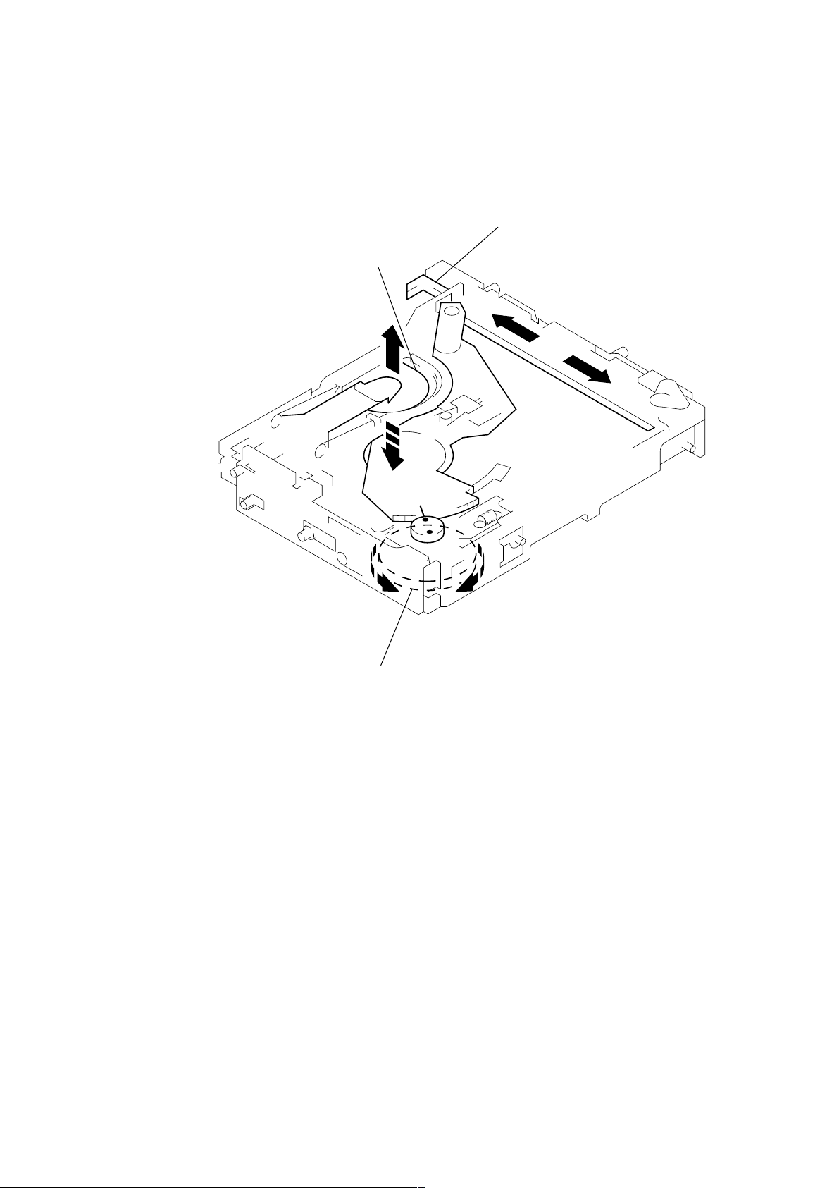
OPERATION CHECK
1
Confirm that the slider moves in the direction of arrow C to move down
the chuck plate if the gear (LOAD CAM) is rotated in the direction of arrow
A
or the chuck plate moves up and the slider moves in the direction of
arrow D if the gear is rotated in the direction of arrow B.
chuck plate
slider
D
C
A
gear (LOAD CAM) assy
B
17
Page 18

MECHANICAL ADJUSTMENTS
• Elevator Height (Address) Adjustment
SECTION 4
Note: This adjustments is necessary when the system controller (IC201),
variable resistor (RV201), slider (R), slider (L), or chassis (ELV)
was replaced for any repair.
Connection:
power supply
(DC 14.4 V)
+
GND
POWER connector (CN303)
wired remote commander
(RM-X82RF)
Compact disc changer
DISPLAY connector (CN302)
Adjustment Method:
1. Load a disc magazine, and place the set vertically as shown
below.
2. Connect the regulated power supply, and turn the power on.
3. Press the DISC button on the wired remote commander (RMX82RF) and select DISC 5.
4. At this time, if the elevator shaft does not position between
comb teeth A and B at addresses 5 and 6 as shown below,
adjust the following.
5. Press repeatedly the DISC + and – buttons on the wired remote commander (RM-X82RF) so that the elevator shafts
moves from address 6 to address 5, or from 5 to 6. At this
time, adjust R V201 on the main board so that the eleva tor shaft
positions smoothly between comb teeth A and B.
6. Further, place the set horizontally and make same adjustment
as mentioned above.
7. After adjustment at addresses 5 to 6 is finished, check all operations from addresses 1 to 10 with the set placed vertically
and horizontally respectively to confirm that the ele vator shaft
positions in a range between comb teeth A to B.
comb tooth at address 6
comb tooth at address 5
comb tooth at address 6
elevator shaft
A
B
OK NG
A
elevator shaft
B
comb tooth at address 5
18
RV201
Page 19

SECTION 5
)
ELECTRICAL CHECK
Note:
1. This adjustment is performed with the set placed horizontally.
2. Power supply voltage: DC14.4 V (more than 3 A).
3. Be sure to use the disc “YEDS-18” parts code: 3-702-101-01, but only
when indicated.
Connection:
power supply
(DC 14.4 V)
+
GND
POWER connector (CN303)
wired remote commander
(RM-X82RF)
FOCUS BIAS CHECK
Connection:
– RF BOARD (Component Side) –
oscilloscope
(AC range)
+
–
TP (VC)
IC101
TP
(RFO)
compact disc changer
DISPLAY connector (CN302)
Procedure:
1. Connect the oscilloscope to TP (RFO) and TP (VC) on the RF
board.
2. Put the set into play mode by loading the disc (YEDS-18).
3. Confirm that oscilloscope waveform is clear and check RF signal level is correct or not.
Note:
Clear RF signal waveform means that the shape “◊” can be clearly distinguished at the center of the waveform.
RF signal waveform
VOLT/DIV: 200 mV
TIME/DIV: 500 ns
(10 : 1 probe in use
level: 1.4 ± 0.3 Vp-p
When observing the eye pattern, set the oscilloscope to AC range
and raise the vertical sensitivity so that it may be easily seen.
19
Page 20

TRACKING OFFSET CHECK
Connection:
– RF BOARD (Component Side) –
oscilloscope
(DC range)
+
–
TP (VC)
IC101
TP (TE)
Procedure:
1. Connect the oscilloscope to TP (TE) and TP (VC) on the RF
board.
2. Put the set into play mode by loading the disc (YEDS-18).
3. Rotate the
[ AMS ] dial on the wired remmote com-
.
>
mander, and check the traverse waveform*.
4. Confirm that the oscilloscope waveform is symmetrical on the
top and bottom in relation to 0 V dc, and check this level.
* Traverse waveform: This is the tracking error wave form appears
when crossing the track.
Traverse waveform
A
0 V
B
A=B
traverse waveform
(100 track jump waveform)
VOLT/DIV: 500 mV
TIME/DIV: 2 ms
Center: 0 V
20
Page 21

6-1. BLOCK DIAGRAM – SERVO Section –
CDX-444RF
SECTION 6
DIAGRAMS
FILTER
DETECTOR
PICK-UP BLOCK
(TRACKING)
(FOCUS)
05
A
B
C
D
E
F
LASER DIODE
PD LD
OPTICAL
(KSS-720A)
2-AXIS DEVICE
I-V AMP
(SPINDLE)
(CHUCKING)
M101
(SLED)
M102
M103
AUTOMATIC
POWER
CONTROL
Q101
M
M
M
FOCUS/TRACKING ERROR AMP
A
5
B
6
C
7
D
8
E
11
F
10
LD
3
TRACKING/FOCUS COIL DRIVE,
SLED/SPINDLE/CHUCKING
VO3+
8
VO3–
9
VO4+
6
VO4–
7
VO2+
10
VO2–
11
VO1+
12
VO1–
13
VL0+
5
VL0–
4
E I-V AMP
F I-V AMP
APC LD
AMP
MOTOR DRIVE
COIL
DRIVE
COIL
DRIVE
MOTOR
DRIVE
MOTOR
DRIVE
MOTOR
DRIVE
SUMMING
IC201
RF AMP,
IC101
RF
AMP
FOCUS
ERROR
AMP
APC PD
VIN3+
VIN3–
VIN4+
VIN4–
VIN2+
VIN2–
VIN1–B
AMP
FWD
REV
RF EQ
AMP
TRACKING
ERROR
AMP
AGC
25
24
31
32
22
21
18
1
2
RFO
LDON
HOLD SW
AGCCONT
63 66 6564
FILI
PCO
FILO
CLTV
RFAC
ASYI
ASYO
DIGITAL SERVO
CLV
ASYMMENTRY
CORRECTOR
RFDC
FE
TE
RFDC
54 50 52 51
RFDC
ANALOG SWITCH
A/D CONVERTER
SIGNAL PROCESS
ON : When the optical pick-up
is inner position
16
FE
14
TE
13
22
21
20
PD
4
TEDR
40
TRDR
41
FFDR
42
FRDR
43
SFDR
38
SRDR
39
MDP
35
61
60
59
LDON
HOLD
AGC
PWM GENERATOR
DIGITAL
FE
FE
OP AMP
TE
TE
MIRR
DFCT
FOK
DIGITAL
SE
PLL
83
EMPH
EFM
DE-
MODULATOR
SUBCODE
PROCESS
SW3
(LIMIT)
D/A
INTER-
FACE
32k RAM
INTERNAL BUS
CORRECTOR
PCMD
LRCK
BCK
ERROR
CPU
INTERFACE
SERVO AUTO
SEQUENCER
SERVO
INTERFACE
SSTP
36
EMPHI
84
79
77
81
GFS
DATA
CLOK
XLAT
SENS
SQSO
SQCK
SCOR
SCLK
FOK
80
78
82
22
13
15
14
16
6
7
24
17
32
11XRST
SERIAL
PCMDI
LRCKI
BCKI
IN
INTERFACE
DIGITAL SIGNAL PROCESSOR,
DIGITAL FILTER, D/A CONVERTER,
DIGITAL SERVO PROCESSOR
IC101
DIGITAL FILTER,
NOISE SHAPER
LDON
HOLD
AGC
54
55
56
91
6
7
5
93
77
79
82
92
90
94
INTEGRATOR
LDON
AGCHOLD
RF AGC
GFS
CDDATA
CDCLK
CDXLT
SENS
SQSO
SQCK
SCOR
SCLK
FOK
XRST
AOUT1
PWM
&
AOUT2
SYSTEM CONTROLLER
IC201 (1/2)
90
97
CLOCK
GENERATOR
AMUTE
FILTER
LOUT
ROUT
XTAO
XTAI
92
GROUND ISOLATION
95
87
86
MUTING
CONTROL
Q401, 402
IC401
X130
16.9344MHz
MUTING
Q410, 420
AIN1
91
LOW-PASS
AIN2
96
TIMING
LOGIC
4
L, R
L
A
(Page 22)
R
• SIGNAL PATH
: CD PLAY
CH. F
71
CH. R
72
LIMSW
89
ON : When completion of the disc
chucking operation
ON : When completion of the disc
save operation
SW1
(CHUCKING END DETECT)
SW2
(SAVE END DETECT)
LOAD1
65
LOAD2
66
2121
Page 22

CDX-444RF
6-2. BLOCK DIAGRAM – MAIN Section –
A
(Page 21)
L, R L
R
L IN
18
R IN
1
GAMMA
AMP
GAMMA
AMP
RV701
TRANSMITTER
L/R BALANCE
MPX
IC701
BUFFER
MPX
OSC
MPX
BAL
MPX
BAL
17 15 6 8
38K
X701
38kHz
38K
MPX
RV702
13
BUFFER
Q701
DEVIATION
RF AMP
Q702, 703
BUFFER, AMP
Q781, 782
PLL
IC781
PD2 FMIN
15 11
PLL
DATA
CLK
CE
5 4 3 1 2
XOUT
XIN
CN703
OUTPUT
M104
(ELEVATOR)
KEYA/D
CN302
DISPLAY
6
M
KEY +5V
ON : When magazine
is set
ELEVATOR
MOTOR DRIVE
IC301
OUT1
9
MOTOR
OUT2
7
DRIVE
KEY ACTIVE
SWITCHING
SWITCH
Q231
Q232
SW201
MAGAZINE
DETECT
IN1
IN2
3
4
X201
12MHz
SYSTEM CONTROLLER
76
MGLK
ELVF
74
73
ELVR
40
XTAL
41
EXTAL
80 KEYACK
95
ADON
58
KEYIN
IC201 (2/2)
PLLDATA
PLLCLK
PLLCE
ACCIN
MCK
EHS
AVREF
ELVON
BUCHK
X781
7.2MHz
PLLDATA
PLLCLK
PLLDATA
98
PLLCLK
97
PLLCE
96
ACCESSORY
+5V
REGULATOR
IC304
LCD +10V
CHECK
Q308
62
RV201
60
59
51
9
BATTERY
CHECK
75
Q301, 302
ELEVATOR HEIGHT
(ADDRESS)
RV202
ELEVATOR HEIGHT
SENSOR
REFERENCE VOLTAGE
D306
HIGH VOLTAGE
DETECT
Q301
SWITCH
Q201
D307
D302
B. UP +5V
BATT B+
MPX +5V
PLLCE
DRIVER +8V
D311
+8V
REGULATOR
IC304
+10V
REGULATOR
Q311
BATT B+
CN303
POWER
3
2
ACC
B. UP
LCDDATA
LCDCLK
LCDCE
LCDINH
POWER ON
05
B. UP +5V
KEY +5V
REGULATOR
CONTROL
Q309, 310
D308
DAC/SERVO +5V
+5V
REGURATOR
Q303
+5V
REGURATOR
IC305
• SIGNAL PATH
: CD PLAY
7
4
5
8
3
+10V
44
45
37
43
LCDDATA
LCDCLK
LCDCE
LCDINH
LCDON
RESET
36
38
SW302
(RESET)
SW301
RESET SIGNAL
GENERATOR
IC303
Z
EJECT
CDON
63
8
B. UP +5V
2222
Page 23

6-3. NOTE FOR PRINTED WIRING BOARDS AND SCHEMATIC DIAGRAMS
• Circuit Boards Location
Note on Printed Wiring Board:
• X : parts extracted from the component side.
• Y : parts extracted from the conductor side.
• W : indicates side identified with part number.
f
•
: internal component.
• b : Pattern from the side which enables seeing.
(The other layers' patterns are not indicated.)
Caution:
Pattern face side: Parts on the pattern face side seen from
(Conductor Side) the pattern face are indicated.
Parts face side: Parts on the par ts face side seen from
(Component Side) the parts face are indicated.
Note on Schematic Diagram:
• All capacitors are in µF unless otherwise noted. pF: µµF
50 WV or less are not indicated except for electrolytics
and tantalums.
• All resistors are in Ω and 1/
specified.
f
•
: internal component.
4
W or less unless otherwise
• C : panel designation.
Note:
The components identified by mark 0 or dotted
line with mark 0 are critical for safety.
Replace only with part
number specified.
Note:
Les composants identifiés par
une marque 0 sont critiques
pour la sécurité.
Ne les remplacer que par une
pièce portant le numéro
spécifié.
• U : B+ Line.
• H : adjustment for repair.
• Power voltage is dc 14.4V and f ed with regulated dc power
supply from CD changer controller.
• Voltages and waveforms are dc with respect to ground
under no-signal conditions.
no mark : CD PLAY
• Voltages are taken with a V OM (Input impedance 10 MΩ).
Voltage variations may be noted due to normal production tolerances.
• Wavef orms are taken with a oscilloscope.
Voltage variations may be noted due to normal production tolerances.
• Circled numbers refer to waveforms.
• Signal path.
J : CD PLAY
SW board
MAIN board
LSW board
FM board
RF board
2323
Page 24

CDX-444RF
6-4. PRINTED WIRING BOARDS – RF/LSW Boards – • See page 23 for Circuit Boards Location.
• Semiconductor
Location
Ref. No. Location
IC101 H-4
IC201 I-3
Q101 F-4
(Page 26)
2424
Page 25

6-5. SCHEMATIC DIAGRAM – RF/LSW Boards – • See page 32 for Waveforms. • See pag e 32 for IC Block Diagrams.
CDX-444RF
(Page 28)
The components identified by mark 0 or dotted
line with mark 0 are critical for safety.
2525
Replace only with part number specified.
Les composants identifiés par une marque 0 sont
critiques pour la sécurité. Ne les remplacer que
par une pièce portant le numéro spécifié.
Page 26

CDX-444RF
6-6. PRINTED WIRING BOARDS – MAIN Board (Component Side) – • See page 23 for Circuit Boards Location.
• Semiconductor
Location
Ref. No. Location
D201 B-6
D202 B-6
D231 F-8
D306 F-5
D307 F-5
D308 G-4
D309 F-4
D310 G-4
D311 F-3
D312 F-6
D313 F-3
IC101 C-8
IC201 F-8
IC301 G-3
IC303 F-3
IC401 C-6
Q201 E-10
Q231 F-7
Q232 F-8
Q301 F-5
Q302 F-5
Q303 F-4
Q401 D-8
Q402 D-8
Q410 C-6
Q420 B-6
(Page 30)
(Page 24)
2626
Page 27

6-7. PRINTED WIRING BOARDS – MAIN (Conductor Side)/SW Boards – • See page 23 for Circuit Boards Location.
CDX-444RF
• Semiconductor
Location
Ref. No. Location
IC304 G-1
IC305 E-1
2727
Page 28

CDX-444RF
6-8. SCHEMATIC DIAGRAM – MAIN Board (1/2) – • See page 32 for Waveforms.
(Page 25)
2828
Page 29

6-9. SCHEMATIC DIAGRAM – MAIN (2/2)/SW Boards – • See page 32 for Waveforms. • See page 32 for IC Block Diagrams.
CDX-444RF
(Page 31)
2929
Page 30

CDX-444RF
6-10. PRINTED WIRING BOARDS – FM Board – • See page 23 for Circuit Boards Location.
(Page 26)
• Semiconductor
Location
Ref. No. Location
D310 B-3
D313 B-1
D701 D-3
D702 D-2
D703 B-4
IC304 C-4
IC701 E-3
IC781 E-4
Q701 D-3
Q702 D-4
Q781 D-2
Q782 C-2
• Semiconductor
Location
Ref. No. Location
D301 B-4
D302 C-4
D311 C-4
D312 C-4
D314 A-1
Q301 A-4
Q308 A-2
Q309 A-3
Q310 A-4
Q311 A-4
Q703 D-4
3030
Page 31

6-11. SCHEMATIC DIAGRAM – FM Board – • See page 32 for Waveforms. • See page 32 for IC Block Diagrams.
CDX-444RF
(Page 29)
3131
Page 32

• Waveforms
– RF Board –
1 IC101 qh (RFO) (CD play mode)
1.4 ± 0.3
Vp-p
– MAIN Board –
1 IC101 uj (LRCK), uk (LRCKI)
(CD play mode)
5.6 Vp-p
– FM Board –
1 IC701 8 (38K) (CD play mode)
4.1 Vp-p
• IC Block Diagrams
– RF Board –
IC101 CXA2596M-T6
1
HOLD
AGCVTH
2
3
LD
4
PD
APC LD
AMP
APC PD
AMP
AGC
24 VCC
23
LC/PD
LD ON
22
21
HOLD SW
20
AGCCONT
2 IC101 qf (FE) (CD play mode)
3 IC101 qd (TE) (CD play mode)
Apporx.
63 mVp-p
Approx.
63 mVp-p
22.8 µs
2 IC101 ia (BCK), is (BCKI)
(CD play mode)
5.7 Vp-p
470 ns
3 IC101 ih (XTAI) (CD play mode)
4.1 Vp-p
60 ns
4 IC101 wf (SCOR),
IC201 is (SCOR) (CD play mode)
13.4 ms
5 IC201 ra (EXTAL) (CD play mode)
4.4 Vp-p
5 Vp-p
26.3 µs
2 IC781 1 (XOUT) (CD play mode)
139 ns
3 IC781 qa (FMIN) (CD play mode)
11.3 ns
2.9 Vp-p
240 mVp-p
5
A
6
VEE
B
7
C
8
D
9
10
F
11
E
12
VC
VCC
VEE
RF SUMMING
AMP
FOCUS ERROR
AMP
F I-V AMP
E I-V AMP
IC201 LA6576L-TE-L
FWD
1
INPUT
2
REV
3
VCC2
4
VLO–
5
VLO+
6
VO4+
7
VO4–
8
VO3+
9
VO3–
10
VO2+
VO2–
11
12
VO1+
VO1–
13
VCC1
14
15
VIN1
COMPARATOR
COMPARATOR
TRACKING
OUTPUT
CONTROL
LEVEL
SHIFT
LEVEL
SHIFT
–
+
LEVEL
SHIFT
LEVEL
SHIFT
–
+
RF EQ
AMP
ERROR
AMP
THERMAL SHUT DOWN
19
RF BOT
18
RFTC
17
RF I
16
RFO
15
RFE
14
FE
13
TE
S-GND
CH1
–
+
–
+
+
–
+
–
36
35
MUTE2
34
MUTE1
33
VIN4
32
VIN4–
31
VIN4+
30
VREF-IN
29
VIN1 (VREF)-SW
28
VREF-OUT (CH1)
27
REG-OUT
REG-IN
26
25
VIN3+
VIN3–
24
VIN3
23
22
VIN2+
21
VIN2–
VIN2
20
VIN1+B
19
–
+
5VREG
+
–
–
+
–
+
CH2-4
MUTE
MUTE
VIN1/VREF
SWITCH
83 ns
VIN1–A
VIN1+A
VIN1–B
3232
16
–
AMP-A
+
17
–
18
AMP-B
+
Page 33

81
80
82
83
84
85
86
87
88
89
90
91
92
93
94
95
96
99
97
98
TIMING
LOGIC
CLOCK
GENERATOR
D/A
INTERFACE
DIGITAL
OUT
32k
RAM
ERROR
CORRECTOR
OVER SAMPLING
DIGITAL FILTER
3rd-ORDER
NOISE SHAPER
LOW-PASS
FILTER
VC
VC
DIGITAL
CLV
MIRR
DFCT
FOK
SERVO
AUTO
SEQUENCER
SERVO
INTERFACE
DIGITAL
PLL
EFM
DEMODULATOR
SUB CODE
PROCESSOR
CPU
INTERFACE
SERIAL-IN
INTERFACE
A/D
CONVERTER
OP AMP
ANALOG
SWITCH
PWM GENERATOR
79 78 77 76 75 74 73 72 71 70 69 68 67 66 65 64 63 62 61 60 59 58 57 56 55
ASYMMETRY
CORRECTOR
54 53 52 51
50
49
47
48
45
44
43
42
41
40
39
38
46
37
36
35
34
33
32
31
302928272625242322212019181716151413121110987654321
FOCUS PWM
GENERATOR
TRACKING PWM
GENERATOR
SLED PWM
GENERATOR
SERVO DSP
FOCUS SERVO
TRACKING
SERVO
SLED SERVO
INTERNAL BUS
PWM
100
LOW-PASS
FILTER
PWM
+
–
+
–
BCK
BCKI
ENPH
EMPHI
XVDD
XTAI
XTAO
XVSS
AVDD1
AOUT1
AIN1
LOUT1
AVSS1
AVSS2
LOUT2
AIN2
RMUT
AOUT2
AVDD2
LMUT
PCMDI
PCMD
LRCKI
LRCK
VDD
ASYE
DOUT
MD2
VSS
VPCO
V16M
VCTL
BIAS
AVDD3
PCO
FILI
FILO
CLTV
AVSS3
RFAC
ASYI
ASYO
AVDD0
IGEN
AVSS0
ADIO
RFDCCETE
SE
FE
VC
TES1
XTSL
VSS
VDD
FRDR
FFDR
TRDR
TFDR
SRDR
SFDR
TEST
FSTIO
SSTP
MDP
LOCK
PWMI
FOK
DFCT
VDD
VSS
MIRR
COUT
WDCK
C4M
SCOR
C2PO
GFS
XPCK
XUGF
WFCK
ATSK
SCKL
SENS
CLOK
XLAT
DATA
SYSM
XRST
EXCK
SBSO
SCSY
SQCK
SQSO
XOLT
SOCK
SOUT
VSS
VDD
– MAIN Board –
IC101 CXD2598Q
IC301 LB1930M-TLM IC304 NJM2395F08
VCC
1
BUFFER
NC
2
IN1
3
4
IN2
S-GND
5
BUFFER
CONTROL
CIRCUIT
MOTOR
DRIVE
CIRCUIT
10
9
8
7
6
NC
OUT1
NC
OUT2
P-GND
IC305 NJM2395F05
2
1
VIN
VOUT
CONTROL
3
GND
4
CONT
33
Page 34

– FM Board –
IC701 BA1405F-E2
AUDIO IN L
MPX MODULATOR
BALANS
MPX MODULATOR
18 17 16 15 14 13 12 11 10
BALANSNCVCC
MPX OUTNCPILOT OUT
NC
L
AMP
MPX
R
AMP
1 2 3 4 5 6 7 8 9
NC
GND
AUDIO IN R
INPUT AMP BIAS
IC781 BU2611AFS-E2
PD2
PD1
VSS
15
16
NC
BUFFER
BUFFER 1/2
OSC 38kHz
NC
NC
38MHz OSC
38MHz OSC
38MHz OSC BIAS
VDD
12 11 10P3914 13
FMIN
AMIN
1
XOUT
PHASE DET,
CHARGE PUMP
REFERENCE DIVIDER
SHIFT REGISTER & LATCH
2
XIN
3CE4CK5DA6
MAIN
COUNT
7
P4
P1
1/16,
1/17
4 BIT
COUNT
8
P2
34
Page 35

6-12. IC PIN FUNCTION DESCRIPTION
• MAIN BOARD IC201 CXP740056-010R (SYSTEM CONTROLLER)
Pin No. Pin Name I/O Description
1 to 3 NC — Not used (open)
4 AMUTE O Audio line muting on/off control signal output “H”: muting on
5 CDXLT O Serial data latch pulse signal output to the CXD2598Q (IC101)
6 CDDATA O Serial data output to the CXD2598Q (IC101)
7 CDCLK O Serial data transfer clock signal output to the CXD2598Q (IC101)
8 CDON O D/A converter and servo section power supply on/off control signal output “H”: power on
9 ELVON O Mechanism deck section power supply on/off control signal output “H”: power on
10 to 35 NC — Not used (open)
36 LCDON O
37 LCDCE O Chip enable signal output to the LCD driver in remote commander
38 RESET I
39 GND — Ground terminal
40 XTAL O Main system clock output terminal (12 MHz)
41 EXTAL I Main system clock input terminal (12 MHz)
42 TEXTSEL I
43 LCDINH O Inhibit signal output to the LCD driver in remote commander
44 LCDDATA O Serial data output to the LCD driver in remote commander
45 LCDCLK O Serial data transfer clock signal output to the LCD driver in remote commander
46 CFSEL I Custom file on/off setting terminal “L” custom file on Not used (open)
47 EEINIT I Initialize signal input for the EEPROM “H”: format Not used (open)
48 EEDATA I/O Two way data bus with the EEPROM Not used(open)
49 EECLK O Sirial data transfer clock signal output to the EEPROM Not used (open)
50 VSS — Ground terminal (for A/D converter)
51 AVREF I Reference voltage (+5V) input terminal (for A/D converter)
52 VDD — Power supply terminal (+5V) (for A/D converter)
53 SINGLE I
54 LDON O The laser automatic power control on/off signal output “H”: automatic power control on
55 AGCHOLD O RF AGC hold on/off signal output “H”: hold on
56 RF AGC O RF AGC level control signal output “L ”: off, center voltage : 40%, “H”: 60%
57 H.TEMP I High temperature sensor input terminal Not used (open)
58 KEYIN I Key input terminal (A/D input) from the remote commander
59 EHS I
60 MCK I
61 NC — Not used (open)
62 ACCIN I Accessory detection signal input “L”: accessory on
63 EJECT I Eject switch (SW301) input terminal “H” active
64 MAGSW I Magazine in/out detection switch input terminal Not used (open)
65 LOAD1 I
The LCD in remote commander and FM transmitter section power supply on/off control signal
output “H”: power on
System reset signal input from the reset switch (SW302) and reset signal generator (IC303)
“L”: reset
For several hundreds msec. after the power supply rises, “L” is input, then it changes to “H”
CD text mode setting terminal “L”: CD text on, “H”: does not display track name
Not used (open)
Setting terminal for the single disc/multiple discs mode
“L”: single mode, “H”: multiple discs mode Not used (open)
Elevator height position detection signal input from the RV202 (elevator height sensor)
(A/D input)
Input of signal for the fine adjustment (elevator height (address) adjustment; RV201) of elevator
position (A/D input)
Chucking end detect switch (SW1) input terminal
“L”: When completion of the disc chucking operation
35
Page 36

Pin No. Pin Name I/O Description
66 LOAD2 I
67 to 70 NC — Not used (open)
71 CH.F O
72 CH.R O
73 ELVR O
74 ELVF O
75 BUCHK I Battery detection signal input “H”: battery on
76 MGLK I Magazine detect switch (SW201) input terminal “L”: magazine is set
77 SQSO I Subcode Q/text serial data input from the CXD2598Q (IC101)
78 NC — Not used (open)
79 SQCK O Subcode Q/text serial data transfer clock signal output to the CXD2598Q (IC101)
80 KEYACK I
81 NC — Not used (open)
82 SCOR I Subcode sync (S0+S1) detection signal input from the CXD2598Q (IC101)
83 SIRCS I SIRCS signal input terminal Not used (open)
84 TEX I Sub system clock input terminal Not used (open)
85 TX O Sub system clock output terminal Not used (open)
86 VSS — Ground terminal
87 VDD — Power supply terminal (+5V)
88 NC — Not used (open)
89 LIMSW I
90 FOK I Focus OK signal input from the CXD2598Q (IC101) “H” is input when focus is on (“L”: NG)
91 GFS I Guard frame sync signal input from the CXD2598Q (IC101) “L”: NG, “H”: OK
92 SCLK O Serial data transfer clock signal output to the CXD2598Q (IC101)
93 SENS I Internal status signal (sense signal) input from the CXD2598Q (IC101)
94 XRST O System reset signal output to the CXD2598Q (IC101) “L”: reset
95 ADON O Power supply on/off control signal output for the A/D converter “L”: power on
96 PLLCE O Chip enable signal output to the PLL IC (IC781)
97 PLLCLK O Serial data transfer clock signal output to the PLL IC (IC781)
98 PLLDATA O Serial data output to the PLL IC (IC781)
99, 100 NC — Not used (open)
Save end detect switch (SW2) input terminal
“L”: When completion of the disc save operation
Motor drive signal (save direction) output to the chucking motor drive (IC201)
“L” active *1
Motor drive signal (chucking direction) output to the chucking motor drive (IC201)
“L” active *1
Motor drive signal (elevator down direction) output to the elevator motor drive (IC301)
“L” active *2
Motor drive signal (elevator up direction) output to the elevator motor drive (IC301)
“L” active *2
Input of acknowledge signal for the key entry
Acknowledge signal is input to accept from the remote commander in the power off status
Sled limit in detect switch (SW3) input terminal
“L”: When the optical pick-up is inner position
*1 chucking motor (M103) control
Terminal
Mode
CH.F (pin ua) “H”“H”“L”“L”
CH.R (pin us) “H”“L”“H”“L”
*2 elevator motor (M104) control
Mode
Terminal
ELVF (pin uf) “H”“L”“H”“L”
ELVR (pin ud) “H”“H”“L”“L”
STOP
STOP
LOAD
CHUCKING
ELEVATORUPELEVATOR
SAVE BRAKE
DOWN
36
BRAKE
Page 37

SECTION 7
2
EXPLODED VIEWS
NOTE:
• -XX and -X mean standardized parts, so they
may have some difference from the original
one.
• Color Indication of Appearance Parts
Example:
KNOB, BALANCE (WHITE) . . . (RED)
↑↑
Parts Color Cabinet's Color
(1) GENERAL SECTION-1
5
6
F1
F2
8
7
• Items marked “*” are not stocked since they
are seldom required for routine service. Some
delay should be anticipated when ordering
these items.
• The mechanical parts with no reference number in the exploded views are not supplied.
• Hardware (# mark) list and accessories and
packing materials are given in the last of the
electrical parts list.
3
#2
The components identified by
mark 0 or dotted line with mark
0 are critical for safety.
Replace only with part number
specified.
Les composants identifiés par une
marque 0 sont critiquens pour la
sécurité.
Ne les remplacer que par une pièce
portant le numéro spécifié.
#2
4
9
#2
1
Ref. No. Part No. Description Remark
1 X-3377-952-1 DOOR (T) ASSY
2 3-039-239-21 PANEL (T), FRONT
3 3-047-886-11 LEVER (FLT)
* 4 3-046-160-11 CASE (UPPER.T)
5 1-792-043-11 CORD (WITH CONNECTOR) (POWER)
6 A-3301-964-A RELAY BOX ASSY
7 1-792-045-21 CORD (WITH CONNECTOR) (ANT-OUT)
10
not supplied
#2
2
#
3
not supplied
Ref. No. Part No. Description Remark
8 1-792-044-21 CORD (WITH CONNECTOR) (CD-OUT)
9 A-3220-787-A WIRED COMMANDER (RM-X82RF)
(GREEN ILLUMINATION)
9 A-3220-788-A WIRED COMMANDER (RM-X82RF)
(AMBER ILLUMINATION)
10 1-792-596-11 CABLE (WITH CONNECTOR) (for RM-X82RF)
F1 1-532-798-11 FUSE (BLADE TYPE) (AUTO FUSE) (1A/32V)
F2 1-532-731-11 FUSE (BLADE TYPE) (AUTO FUSE) (3A/32V)
37
Page 38

(2) GENERAL SECTION-2
not
supplied
#1
56
57
55
63
54
65
62
58
51
#3
64
not
supplied
53
61
60
59
#3
66
67
#3
RV202
69
MG-251A-137
66
68
60
71
not supplied
not supplied
Ref. No. Part No. Description Remark
51 3-047-852-01 DAMPER (T)
* 52 X-3378-122-1 CASE (LOWER. T) ASSY
* 53 A-3326-027-A FM BOARD, COMPLETE
* 54 3-046-989-01 PLATE (FM), SHIELD
55 3-225-783-01 SPRING (GROUND)
56 1-676-735-11 FM FLEXIBLE BOARD
57 3-042-999-11 COVER (FM CONNECTOR. T)
58 3-913-406-11 SCREW (GROUND)
59 X-3375-357-1 ARM (FLT) ASSY
60 3-935-636-11 SCREW (FP)
* 61 1-676-722-11 SW BOARD
51
52
Ref. No. Part No. Description Remark
62 3-042-244-11 SCREW (T)
63 3-041-218-21 ESCUTCHEON (T)
64 3-022-007-01 BUTTON (EJT) (Z)
* 65 3-022-012-01 HEAT SINK (T)
66 3-038-166-01 SPRING (FL), TENSION COIL
* 67 A-3283-116-A MAIN BOARD, COMPLETE
68 1-676-339-11 MAIN FLEXIBLE BOARD
* 69 3-046-988-01 PLATE (MAIN), SHIELD
71 X-3375-360-1 ARM (FRT) ASSY
RV202 1-227-137-11 RES, VAR, SLIDE 10K
(ELEVATOR HEIGHT SENSOR)
38
Page 39

(3) MECHANISM DECK SECTION-1
(MG-251A-137)
#3
101
#3
#3
102
103
Ref. No. Part No. Description Remark
101 X-3378-091-1 CHASSIS (U. S) SUB ASSY
102 3-024-161-11 SPRING (SUT)
Ref. No. Part No. Description Remark
103 3-011-997-01 SPRING (STOPPER. LOWER)
39
Page 40

(4) MECHANISM DECK SECTION-2
(MG-251A-137)
#3
152
M104
151
Ref. No. Part No. Description Remark
151 3-024-170-01 SPRING (SB), TENSION
* 152 3-040-790-01 BRACKET (EVM. S)
153
Ref. No. Part No. Description Remark
153 X-3378-092-1 CHASSIS (D. S) SUB ASSY
M104 A-3301-123-A ELJ MOTOR ASSY (ELEVATOR)
40
Page 41

(5) MECHANISM DECK SECTION-3
(MG-251A-137)
211
#8
213
212
#4
210
202
M103
201
#3
#6
204
205
209
206
208
#8
207
#3
214
#6
#6
Ref. No. Part No. Description Remark
* 201 3-024-150-01 RETAINER (CHM)
* 202 X-3378-080-1 BRACKET (CHM. D) ASSY
204 3-321-813-01 WASHER, COTTER POLYETHYLENE
205 3-017-139-01 GEAR (WORM LOAD A)
206 3-022-839-01 ARM (NSW)
207 3-573-936-00 STOPPER, REEL
208 X-3375-220-1 GEAR (LOAD CAM) ASSY
Ref. No. Part No. Description Remark
209 3-010-252-11 ROLLER (CRE)
210 3-010-268-01 SPRING (DH), TENSION
* 211 A-3290-194-C MAIN ASSY, CHASSIS (EVY)
212 3-010-254-11 SHAFT (ROTARY PREVENTION C)
213 3-010-253-01 GEAR (LOMINI)
* 214 A-3326-000-A RF BOARD, COMPLETE
M103 A-3301-123-A ELJ MOTOR ASSY (CHUCKING)
41
Page 42

(6) MECHANISM DECK SECTION-4
(MG-251A-137)
258
256
#7
254
#9
257
252
M101
#5
not supplied
255
#5
#10
259
M102
not supplied
251
253
#11
not supplied
Ref. No. Part No. Description Remark
251 1-676-341-11 OP FLEXIBLE BOARD
252 3-025-743-01 SPRING (FEED), LEAF
253 X-3378-101-1 HOLDER (SLED. S) ASSY
254 3-931-832-01 GEAR (SL MIDWAY)
0 255 8-820-103-05 OPTICAL PICK-UP KSS-720A/Q-RP
256 A-3291-669-A SHAFT (FEED) ASSY
The components identified by
mark 0 or dotted line with
mark 0 are critical for safety .
Replace only with part number specified.
Ref. No. Part No. Description Remark
257 3-010-263-01 DETENT (SHAFT THRUST)
* 258 1-676-524-11 LSW BOARD
259 A-3301-954-A BASE (OPT. S) (J) ASSY
M101 A-3315-151-A SLED MOTOR ASSY (251)
M102 A-3301-998-A SPINDLE MOTOR (S) SUB ASSY
Les composants identifiés par une
marque 0 sont critiques pour la
sécurité.
Ne les remplacer que par une pièce
portant le numéro spécifié.
42
Page 43

SECTION 8
ELECTRICAL PARTS LIST
FM
NOTE:
• Due to standardization, replacements in the
parts list may be different from the parts specified in the diagrams or the components used
on the set.
• -XX and -X mean standardized parts, so they
may have some difference from the original
one.
• RESISTORS
All resistors are in ohms.
METAL: Metal-film resistor.
METAL OXIDE: Metal oxide-film resistor.
F: nonflammable
Ref. No. Part No. Description Remark Ref. No. Part No. Description Remark
* A-3326-027-A FM BOARD, COMPLETE
*******************
< CAPACITOR >
C301 1-163-809-11 CERAMIC CHIP 0.047uF 10% 25V
C303 1-127-820-11 CERAMIC CHIP 4.7uF 16V
C304 1-109-982-11 CERAMIC CHIP 1uF 10% 10V
C305 1-128-499-11 ELECT 220uF 20% 16V
C319 1-109-982-11 CERAMIC CHIP 1uF 10% 10V
C320 1-115-866-11 ELECT 4.7uF 20% 35V
C322 1-125-972-61 ELECT 100uF 20% 16V
C323 1-125-837-11 CERAMIC CHIP 1uF 10% 6.3V
C324 1-124-584-00 ELECT 100uF 20% 10V
C325 1-162-927-11 CERAMIC CHIP 100PF 5% 50V
C326 1-162-927-11 CERAMIC CHIP 100PF 5% 50V
C328 1-162-927-11 CERAMIC CHIP 100PF 5% 50V
C329 1-162-927-11 CERAMIC CHIP 100PF 5% 50V
C331 1-162-927-11 CERAMIC CHIP 100PF 5% 50V
C701 1-126-514-11 ELECT 22uF 20% 10V
C702 1-163-009-11 CERAMIC CHIP 0.001uF 10% 50V
C703 1-162-915-11 CERAMIC CHIP 10PF 0.5PF 50V
C704 1-162-927-11 CERAMIC CHIP 100PF 5% 50V
C705 1-115-866-11 ELECT 4.7uF 20% 35V
C706 1-162-927-11 CERAMIC CHIP 100PF 5% 50V
• Items marked “*” are not stocked since they
are seldom required for routine service.
Some delay should be anticipated when ordering these items.
• SEMICONDUCTORS
In each case, u: µ, for example:
uA. . : µA. . uPA. . : µPA. .
uPB. . : µPB. . uPC. . : µPC. .
uPD. . : µPD. .
• CAPACITORS
uF: µF
• COILS
uH: µH
C784 1-162-970-11 CERAMIC CHIP 0.01uF 10% 25V
C785 1-126-514-11 ELECT 22uF 20% 10V
C786 1-165-176-11 CERAMIC CHIP 0.047uF 10% 16V
C787 1-165-176-11 CERAMIC CHIP 0.047uF 10% 16V
C788 1-109-982-11 CERAMIC CHIP 1uF 10% 10V
CN302 1-794-066-11 CONNECTOR, MINIATURE DIN 8P (DISPLAY)
CN303 1-793-286-11 PIN, CONNECTOR (PC BOARD) 3P (POWER)
CN701 1-784-829-21 CONNECTOR, FPC 21P
CN703 1-566-822-41 JACK (OUTPUT)
D301 8-719-029-25 DIODE DSA3A4-F2
D302 8-719-022-90 DIODE MA8160-M
D310 8-719-423-23 DIODE MA8110-M
D311 8-719-977-12 DIODE DTZ6.8B
D312 8-719-801-78 DIODE 1SS184
D313 8-719-977-12 DIODE DTZ6.8B
D314 8-719-977-12 DIODE DTZ6.8B
D701 8-719-058-78 DIODE HVU202A3TRF
D702 8-719-988-61 DIODE 1SS355TE-17
D703 8-719-988-61 DIODE 1SS355TE-17
The components identified by
mark 0 or dotted line with mark
0 are critical for safety.
Replace only with part number
specified.
Les composants identifiés par une
marque 0 sont critiquens pour la
sécurité.
Ne les remplacer que par une pièce
portant le numéro spécifié.
When indicating parts by reference
number, please include the board.
< CONNECTOR/JACK >
< DIODE >
< IC >
C707 1-162-997-11 CERAMIC CHIP 10PF 0.5PF 50V
C708 1-162-915-11 CERAMIC CHIP 10PF 0.5PF 50V
C709 1-162-916-11 CERAMIC CHIP 12PF 5% 50V
C710 1-162-917-11 CERAMIC CHIP 15PF 5% 50V
C711 1-162-913-11 CERAMIC CHIP 8PF 0.5PF 50V
C712 1-162-970-11 CERAMIC CHIP 0.01uF 10% 25V
C713 1-162-923-11 CERAMIC CHIP 47PF 5% 50V
C714 1-163-243-11 CERAMIC CHIP 47PF 5% 50V
C715 1-107-725-11 CERAMIC CHIP 0.1uF 10% 16V
C716 1-109-982-11 CERAMIC CHIP 1uF 10% 10V
C720 1-162-970-11 CERAMIC CHIP 0.01uF 10% 25V
C741 1-162-964-11 CERAMIC CHIP 0.001uF 10% 50V
C742 1-162-964-11 CERAMIC CHIP 0.001uF 10% 50V
C743 1-115-872-11 ELECT 2.2uF 20% 50V
C761 1-162-964-11 CERAMIC CHIP 0.001uF 10% 50V
C762 1-162-964-11 CERAMIC CHIP 0.001uF 10% 50V
C763 1-115-872-11 ELECT 2.2uF 20% 50V
C781 1-162-920-11 CERAMIC CHIP 27PF 5% 50V
C782 1-162-920-11 CERAMIC CHIP 27PF 5% 50V
C783 1-162-970-11 CERAMIC CHIP 0.01uF 10% 25V
IC304 8-759-711-59 IC NJM78L05UA-TE1
IC701 8-759-393-50 IC BA1405F-E2
IC781 8-759-595-05 IC BU2611AFS-E2
< COIL >
L301 1-419-545-11 INDUCTOR 1mH
L701 1-419-467-11 COIL, IFT
L702 1-411-845-11 COIL, AIR-CORE
L703 1-410-997-42 INDUCTOR CHIP 2.2uH
< TRANSISTOR >
Q301 8-729-900-53 TRANSISTOR DTC114EK
Q308 8-729-120-28 TRANSISTOR 2SC1623-L5L6
Q309 1-801-806-11 TRANSISTOR DTC144EKA
Q310 8-729-027-31 TRANSISTOR DTA124EKA-T146
Q311 8-729-106-68 TRANSISTOR 2SD1615A-GP
Q701 8-729-120-28 TRANSISTOR 2SC1623-L5L6
Q702 8-729-804-72 TRANSISTOR 2SC2814-F4
Q703 8-729-804-72 TRANSISTOR 2SC2814-F4
Q781 8-729-120-28 TRANSISTOR 2SC1623-L5L6
43
Page 44

FM LSW MAIN
Ref. No. Part No. Description Remark
Q782 8-729-120-28 TRANSISTOR 2SC1623-L5L6
< RESISTOR >
R301 1-216-057-00 METAL CHIP 2.2K 5% 1/10W
R310 1-216-089-11 RES-CHIP 47K 5% 1/10W
R311 1-216-085-00 METAL CHIP 33K 5% 1/10W
R312 1-216-841-11 METAL CHIP 47K 5% 1/16W
R313 1-216-206-00 RES-CHIP 2.2K 5% 1/8W
R315 1-216-041-00 METAL CHIP 470 5% 1/10W
R316 1-216-025-11 RES-CHIP 100 5% 1/10W
R317 1-216-041-00 METAL CHIP 470 5% 1/10W
R319 1-216-041-00 METAL CHIP 470 5% 1/10W
R320 1-216-041-00 METAL CHIP 470 5% 1/10W
R321 1-216-041-00 METAL CHIP 470 5% 1/10W
R399 1-216-296-00 SHORT 0
R701 1-216-850-11 METAL CHIP 270K 5% 1/16W
R702 1-216-835-11 METAL CHIP 15K 5% 1/16W
R703 1-216-818-11 METAL CHIP 560 5% 1/16W
R704 1-216-809-11 METAL CHIP 100 5% 1/16W
R705 1-216-828-11 METAL CHIP 3.9K 5% 1/16W
R706 1-216-833-11 METAL CHIP 10K 5% 1/16W
R707 1-216-833-11 METAL CHIP 10K 5% 1/16W
R708 1-216-834-11 METAL CHIP 12K 5% 1/16W
R709 1-216-821-11 METAL CHIP 1K 5% 1/16W
R710 1-216-833-11 METAL CHIP 10K 5% 1/16W
R711 1-216-826-11 METAL CHIP 2.7K 5% 1/16W
R712 1-216-817-11 METAL CHIP 470 5% 1/16W
R713 1-216-845-11 METAL CHIP 100K 5% 1/16W
R714 1-216-815-11 METAL CHIP 330 5% 1/16W
R715 1-216-809-11 METAL CHIP 100 5% 1/16W
R716 1-216-037-00 METAL CHIP 330 5% 1/10W
R717 1-216-025-11 RES-CHIP 100 5% 1/10W
R741 1-216-821-11 METAL CHIP 1K 5% 1/16W
R742 1-216-833-11 METAL CHIP 10K 5% 1/16W
R743 1-216-840-11 METAL CHIP 39K 5% 1/16W
R745 1-216-071-00 METAL CHIP 8.2K 5% 1/10W
R746 1-216-057-00 METAL CHIP 2.2K 5% 1/10W
R761 1-216-821-11 METAL CHIP 1K 5% 1/16W
R762 1-216-833-11 METAL CHIP 10K 5% 1/16W
R763 1-216-840-11 METAL CHIP 39K 5% 1/16W
R765 1-216-071-00 METAL CHIP 8.2K 5% 1/10W
R766 1-216-057-00 METAL CHIP 2.2K 5% 1/10W
R781 1-216-837-11 METAL CHIP 22K 5% 1/16W
R782 1-216-833-11 METAL CHIP 10K 5% 1/16W
R783 1-216-819-11 METAL CHIP 680 5% 1/16W
R784 1-216-689-11 METAL CHIP 39K 0.5% 1/10W
R787 1-216-057-00 RES-CHIP 2.2K 5% 1/10W
R788 1-216-049-11 RES-CHIP 1K 5% 1/10W
R789 1-216-049-11 RES-CHIP 1K 5% 1/10W
Ref. No. Part No. Description Remark
* 1-676-524-13 LSW BOARD
***********
< SWITCH >
SW3 1-529-565-41 SWITCH, PUSH (1 KEY) (LIMIT)
**************************************************************
* A-3283-116-A MAIN BOARD, COMPLETE
*********************
1-676-339-12 MAIN FLEXIBLE BOARD
* 3-046-988-01 PLATE (MAIN) , SHIELD
< CAPACITOR >
C101 1-164-360-11 CERAMIC CHIP 0.1uF 16V
C102 1-164-360-11 CERAMIC CHIP 0.1uF 16V
C103 1-164-360-11 CERAMIC CHIP 0.1uF 16V
C104 1-162-970-11 CERAMIC CHIP 0.01uF 10% 25V
C110 1-162-965-11 CERAMIC CHIP 0.0015uF 10% 50V
C111 1-162-965-11 CERAMIC CHIP 0.0015uF 10% 50V
C112 1-115-467-11 CERAMIC CHIP 0.22uF 10% 10V
C120 1-162-967-11 CERAMIC CHIP 0.0033uF 10% 50V
C121 1-164-360-11 CERAMIC CHIP 0.1uF 16V
C122 1-115-566-11 CERAMIC CHIP 4.7uF 10% 10V
C123 1-162-970-11 CERAMIC CHIP 0.01uF 10% 25V
C124 1-162-965-11 CERAMIC CHIP 0.0015uF 10% 50V
C125 1-165-176-11 CERAMIC CHIP 0.047uF 10% 16V
C126 1-164-360-11 CERAMIC CHIP 0.1uF 16V
C127 1-162-960-11 CERAMIC CHIP 220PF 10% 50V
C129 1-164-360-11 CERAMIC CHIP 0.1uF 16V
C130 1-164-360-11 CERAMIC CHIP 0.1uF 16V
C140 1-162-963-11 CERAMIC CHIP 680PF 10% 50V
C141 1-162-963-11 CERAMIC CHIP 680PF 10% 50V
C142 1-164-217-11 CERAMIC CHIP 150PF 5% 50V
C143 1-164-217-11 CERAMIC CHIP 150PF 5% 50V
C144 1-126-382-11 ELECT 100uF 20% 16V
C145 1-126-382-11 ELECT 100uF 20% 16V
C201 1-107-826-11 CERAMIC CHIP 0.1uF 10% 16V
C203 1-164-360-11 CERAMIC CHIP 0.1uF 16V
C204 1-164-360-11 CERAMIC CHIP 0.1uF 16V
C205 1-164-360-11 CERAMIC CHIP 0.1uF 16V
C301 1-164-360-11 CERAMIC CHIP 0.1uF 16V
C302 1-164-360-11 CERAMIC CHIP 0.1uF 16V
C303 1-164-360-11 CERAMIC CHIP 0.1uF 16V
C307 1-165-112-11 CERAMIC CHIP 0.33uF 20% 10V
C308 1-125-837-11 CERAMIC CHIP 1uF 10% 6.3V
C309 1-164-360-11 CERAMIC CHIP 0.1uF 16V
C310 1-125-701-11 DOUBLE LAYER 0.047F 5.5V
C311 1-126-382-11 ELECT 100uF 20% 16V
< VARIABLE RESISTOR >
RV701 1-238-092-11 RES, ADJ, CERMET 47K
RV702 1-238-086-11 RES, ADJ, CERMET 470
< VIBRATOR >
X701 1-567-093-00 VIBRATOR, CRYSTAL (38kHz)
X781 1-760-838-21 VIBRATOR, CRYSTAL (7.2MHz)
**************************************************************
44
C312 1-115-156-11 CERAMIC CHIP 1uF 10V
C313 1-126-382-11 ELECT 100uF 20% 16V
C314 1-164-360-11 CERAMIC CHIP 0.1uF 16V
C315 1-115-466-00 ELECT 1000uF 20% 16V
C316 1-126-382-11 ELECT 100uF 20% 16V
C317 1-164-360-11 CERAMIC CHIP 0.1uF 16V
C318 1-126-382-11 ELECT 100uF 20% 16V
C319 1-164-360-11 CERAMIC CHIP 0.1uF 16V
C320 1-162-970-11 CERAMIC CHIP 0.01uF 10% 25V
Page 45

MAIN
Ref. No. Part No. Description Remark
C401 1-162-962-11 CERAMIC CHIP 470PF 10% 50V
C402 1-162-962-11 CERAMIC CHIP 470PF 10% 50V
C404 1-126-157-11 ELECT 10uF 20% 16V
C405 1-126-157-11 ELECT 10uF 20% 16V
C406 1-162-927-11 CERAMIC CHIP 100PF 5% 50V
C407 1-162-927-11 CERAMIC CHIP 100PF 5% 50V
C416 1-126-382-11 ELECT 100uF 20% 16V
< CONNECTOR >
CN231 1-784-829-21 CONNECTOR, FPC 21P
< DIODE >
D201 8-719-978-33 DIODE DTZ-TT11-6.8B
D202 8-719-978-33 DIODE DTZ-TT11-6.8B
D231 8-719-988-61 DIODE 1SS355TE-17
D306 8-719-069-56 DIODE UDZS-TE17-6.2B
D307 8-719-988-61 DIODE 1SS355TE-17
D308 8-719-914-44 DIODE DAP202K
D309 8-719-988-61 DIODE 1SS355TE-17
D310 8-719-422-67 DIODE MA8062-H
D311 8-719-978-33 DIODE DTZ-TT11-6.8B
D312 8-719-978-33 DIODE DTZ-TT11-6.8B
D313 8-719-978-33 DIODE DTZ-TT11-6.8B
< IC >
IC101 8-752-392-04 IC CXD2598Q
IC201 8-752-921-24 IC CXP740056-010R
IC301 8-759-527-33 IC LB1930M-TLM
IC303 8-759-363-81 IC XC61AN4002PR
IC304 8-759-655-30 IC NJM2395F08
IC305 8-759-655-29 IC NJM2395F05
IC401 8-759-662-11 IC TLV2362IPWR
< COIL >
L140 1-412-058-11 INDUCTOR CHIP 10uH
Ref. No. Part No. Description Remark
R121 1-216-845-11 METAL CHIP 100K 5% 1/16W
R122 1-216-845-11 METAL CHIP 100K 5% 1/16W
R123 1-216-833-11 METAL CHIP 10K 5% 1/16W
R124 1-216-827-11 METAL CHIP 3.3K 5% 1/16W
R125 1-216-827-11 METAL CHIP 3.3K 5% 1/16W
R126 1-216-857-11 METAL CHIP 1M 5% 1/16W
R140 1-216-834-11 METAL CHIP 12K 5% 1/16W
R141 1-216-834-11 METAL CHIP 12K 5% 1/16W
R142 1-216-834-11 METAL CHIP 12K 5% 1/16W
R143 1-216-834-11 METAL CHIP 12K 5% 1/16W
R144 1-216-834-11 METAL CHIP 12K 5% 1/16W
R145 1-216-834-11 METAL CHIP 12K 5% 1/16W
R146 1-216-833-11 METAL CHIP 10K 5% 1/16W
R147 1-216-833-11 METAL CHIP 10K 5% 1/16W
R201 1-216-821-11 METAL CHIP 1K 5% 1/16W
R207 1-216-845-11 METAL CHIP 100K 5% 1/16W
R209 1-216-833-11 METAL CHIP 10K 5% 1/16W
R232 1-216-845-11 METAL CHIP 100K 5% 1/16W
R233 1-216-833-11 METAL CHIP 10K 5% 1/16W
R234 1-216-821-11 METAL CHIP 1K 5% 1/16W
R252 1-216-845-11 METAL CHIP 100K 5% 1/16W
R253 1-216-845-11 METAL CHIP 100K 5% 1/16W
R254 1-216-845-11 METAL CHIP 100K 5% 1/16W
R302 1-216-845-11 METAL CHIP 100K 5% 1/16W
R303 1-216-846-11 METAL CHIP 120K 5% 1/16W
R304 1-216-847-11 METAL CHIP 150K 5% 1/16W
R305 1-216-841-11 METAL CHIP 47K 5% 1/16W
R306 1-216-844-11 METAL CHIP 82K 5% 1/16W
R311 1-216-841-11 METAL CHIP 47K 5% 1/16W
R315 1-216-864-11 METAL CHIP 0 5% 1/16W
R401 1-216-833-11 METAL CHIP 10K 5% 1/16W
R402 1-216-833-11 METAL CHIP 10K 5% 1/16W
R403 1-216-833-11 METAL CHIP 10K 5% 1/16W
R404 1-216-833-11 METAL CHIP 10K 5% 1/16W
R405 1-216-833-11 METAL CHIP 10K 5% 1/16W
R406 1-216-833-11 METAL CHIP 10K 5% 1/16W
< TRANSISTOR >
Q201 8-729-020-67 TRANSISTOR XN1A312-TX
Q231 8-729-027-23 TRANSISTOR DTA114EKA-T146
Q232 8-729-027-23 TRANSISTOR DTA114EKA-T146
Q301 8-729-028-62 TRANSISTOR DTA115EKA-T146
Q302 8-729-230-49 TRANSISTOR 2SC2712-YG
Q303 8-729-921-12 TRANSISTOR 2SD1834
Q401 8-729-901-00 TRANSISTOR DTC124EK
Q402 8-729-027-23 TRANSISTOR DTA114EKA-T146
Q410 8-729-015-39 TRANSISTOR DTC323TK
Q420 8-729-015-39 TRANSISTOR DTC323TK
< RESISTOR >
R101 1-216-833-11 METAL CHIP 10K 5% 1/16W
R111 1-216-833-11 METAL CHIP 10K 5% 1/16W
R112 1-216-845-11 METAL CHIP 100K 5% 1/16W
R114 1-216-833-11 METAL CHIP 10K 5% 1/16W
R115 1-216-833-11 METAL CHIP 10K 5% 1/16W
R116 1-216-837-11 METAL CHIP 22K 5% 1/16W
R117 1-216-845-11 METAL CHIP 100K 5% 1/16W
R120 1-216-839-11 METAL CHIP 33K 5% 1/16W
R407 1-216-833-11 METAL CHIP 10K 5% 1/16W
R408 1-216-833-11 METAL CHIP 10K 5% 1/16W
R411 1-216-813-11 METAL CHIP 220 5% 1/16W
R412 1-216-813-11 METAL CHIP 220 5% 1/16W
R413 1-216-845-11 METAL CHIP 100K 5% 1/16W
R414 1-216-845-11 METAL CHIP 100K 5% 1/16W
R415 1-216-864-11 METAL CHIP 0 5% 1/16W
R416 1-216-864-11 METAL CHIP 0 5% 1/16W
R420 1-216-864-11 METAL CHIP 0 5% 1/16W
< VARIABLE RESISTOR >
RV201 1-223-834-11 RES, ADJ, CARBON 47K
< SWITCH >
SW201 1-529-565-41 SWITCH, PUSH (1 KEY) (MAGAZINE DETECT)
< VIBRATOR >
X130 1-760-307-11 VIBRATOR, CERAMIC (16.9344MHz)
X201 1-579-126-11 VIBRATOR, CERAMIC (12MHz)
**************************************************************
45
Page 46

RF SW
Ref. No. Part No. Description Remark
* A-3326-000-A RF BOARD, COMPLETE
*******************
< CAPACITOR >
C101 1-107-826-11 CERAMIC CHIP 0.1uF 10% 16V
C102 1-126-206-11 ELECT CHIP 100uF 20% 6.3V
C103 1-162-970-11 CERAMIC CHIP 0.01uF 10% 25V
C104 1-107-826-11 CERAMIC CHIP 0.1uF 10% 16V
C105 1-125-837-11 CERAMIC CHIP 1uF 10% 6.3V
C106 1-126-206-11 ELECT CHIP 100uF 20% 6.3V
C107 1-162-915-11 CERAMIC CHIP 10PF 0.5PF 50V
C108 1-124-779-00 ELECT CHIP 10uF 20% 16V
C109 1-107-826-11 CERAMIC CHIP 0.1uF 10% 16V
C110 1-126-206-11 ELECT CHIP 100uF 20% 6.3V
C111 1-124-779-00 ELECT CHIP 10uF 20% 16V
C201 1-117-681-11 ELECT CHIP 100uF 20% 16V
C202 1-107-826-11 CERAMIC CHIP 0.1uF 10% 16V
C203 1-162-962-11 CERAMIC CHIP 470PF 10% 50V
C204 1-162-962-11 CERAMIC CHIP 470PF 10% 50V
C205 1-162-962-11 CERAMIC CHIP 470PF 10% 50V
C206 1-162-962-11 CERAMIC CHIP 470PF 10% 50V
C207 1-164-227-11 CERAMIC CHIP 0.022uF 10% 25V
C208 1-164-227-11 CERAMIC CHIP 0.022uF 10% 25V
C209 1-164-227-11 CERAMIC CHIP 0.022uF 10% 25V
C217 1-107-826-11 CERAMIC CHIP 0.1uF 10% 16V
< CONNECTOR >
CN102 1-778-303-21 CONNECTOR, FPC (ZIF) 16P
CNJ101 1-778-777-21 CONNECTOR, FPC 26P
< IC >
IC101 8-752-095-36 IC CXA2596M-T6
IC201 8-759-832-99 IC LA6576L-TE-L
< TRANSISTOR >
Ref. No. Part No. Description Remark
R210 1-216-842-11 METAL CHIP 56K 5% 1/16W
R211 1-216-833-11 METAL CHIP 10K 5% 1/16W
R212 1-216-839-11 METAL CHIP 33K 5% 1/16W
R213 1-216-833-11 METAL CHIP 10K 5% 1/16W
R214 1-216-839-11 METAL CHIP 33K 5% 1/16W
R215 1-216-839-11 METAL CHIP 33K 5% 1/16W
R216 1-216-842-11 METAL CHIP 56K 5% 1/16W
R218 1-216-839-11 METAL CHIP 33K 5% 1/16W
R219 1-216-843-11 METAL CHIP 68K 5% 1/16W
R220 1-216-834-11 METAL CHIP 12K 5% 1/16W
R222 1-216-821-11 METAL CHIP 1K 5% 1/16W
R223 1-216-821-11 METAL CHIP 1K 5% 1/16W
< SWITCH >
SW1 1-529-566-41 SWITCH, PUSH (1 KEY)
(CHUCKING END DETECT)
SW2 1-529-566-41 SWITCH, PUSH (1 KEY) (SAVE END DETECT)
**************************************************************
* 1-676-722-12 SW BOARD
*********
< SWITCH >
SW301 1-571-532-21 SWITCH, TACTIL (Z)
SW302 1-571-532-21 SWITCH, TACTIL (RESET)
**************************************************************
MISCELLANEOUS
**************
5 1-792-043-11 CORD (WITH CONNECTOR) (POWER)
7 1-792-045-21 CORD (WITH CONNECTOR) (ANT-OUT)
8 1-792-044-21 CORD (WITH CONNECTOR) (CD-OUT)
9 A-3220-787-A WIRED COMMANDER (RM-X82RF)
(GREEN ILLUMINATION)
9 A-3220-788-A WIRED COMMANDER (RM-X82RF)
(AMBER ILLUMINATION)
Q101 8-729-141-48 TRANSISTOR 2SB624-BV345
< RESISTOR >
R101 1-216-847-11 METAL CHIP 150K 5% 1/16W
R102 1-216-847-11 METAL CHIP 150K 5% 1/16W
R103 1-216-864-11 METAL CHIP 0 5% 1/16W
R104 1-216-158-00 RES-CHIP 22 5% 1/8W
R105 1-216-857-11 METAL CHIP 1M 5% 1/16W
R106 1-216-857-11 METAL CHIP 1M 5% 1/16W
R107 1-216-864-11 METAL CHIP 0 5% 1/16W
R108 1-216-845-11 METAL CHIP 100K 5% 1/16W
R109 1-216-837-11 METAL CHIP 22K 5% 1/16W
R110 1-216-821-11 METAL CHIP 1K 5% 1/16W
R201 1-216-826-11 METAL CHIP 2.7K 5% 1/16W
R202 1-216-833-11 METAL CHIP 10K 5% 1/16W
R203 1-216-833-11 METAL CHIP 10K 5% 1/16W
R204 1-216-842-11 METAL CHIP 56K 5% 1/16W
R205 1-216-833-11 METAL CHIP 10K 5% 1/16W
R206 1-216-842-11 METAL CHIP 56K 5% 1/16W
R207 1-216-833-11 METAL CHIP 10K 5% 1/16W
R208 1-216-842-11 METAL CHIP 56K 5% 1/16W
R209 1-216-833-11 METAL CHIP 10K 5% 1/16W
46
10 1-792-596-11 CABLE (WITH CONNECTOR) (for RM-X82RF)
56 1-676-735-11 FM FLEXIBLE BOARD
251 1-676-341-11 OP FLEXIBLE BOARD
0 255 8-820-103-05 OPTICAL PICK-UP KSS-720A/Q-RP
F1 1-532-798-11 FUSE (BLADE TYPE) (AUTO FUSE) (1A/32V)
F2 1-532-731-11 FUSE (BLADE TYPE) (AUTO FUSE) (3A/32V)
M101 A-3315-151-A SLED MOTOR ASSY (251)
M102 A-3301-998-A SPINDLE MOTOR (S) SUB ASSY
M103 A-3301-123-A ELJ MOTOR ASSY (CHUCKING)
M104 A-3301-123-A ELJ MOTOR ASSY (ELEVATOR)
RV202 1-227-137-11 RES, VAR, SLIDE 10K
************************************************************
The components identified by
mark 0 or dotted line with
mark 0 are critical for safety .
Replace only with part number specified.
(ELEVATOR HEIGHT SENSOR)
Les composants identifiés par une
marque 0 sont critiques pour la
sécurité.
Ne les remplacer que par une pièce
portant le neméro spécifié.
Page 47

Ref. No. Part No. Description Remark
**************
HARDWARE LIST
**************
#1 7-685-862-09 SCREW +BVTT 2.6X6 (S)
#2 7-685-792-09 SCREW +PTT 2.6X6 (S)
#3 7-685-781-09 SCREW +PTT 2X4 (S)
#4 7-624-104-04 STOP RING 2.0, TYPE -E
#5 7-627-554-07 SCREW, PRECISION +P 2X2.2
#6 7-628-253-00 SCREW +PS 2X4
#7 7-627-553-27 SCREW, PRECISION +P 2X2.5
#8 7-624-102-04 STOP RING 1.5, TYPE -E
#9 7-627-850-28 SCREW, PRECISION +P 1.4X3
#10 7-627-000-00 SCREW, PRECISION +P 1.7X2.2 TYPE 3
Ref. No. Part No. Description Remark
501 502
BRACKET (T)
× 2
+PSW4 × 10
× 4
TAPPING SCREW
(DIA.5 × 20) × 4
503
#11 7-627-553-37 PRECISION SCREW +P 2X3 TYPE 3
************************************************************
ACCESSORIES & PACKING MATERIALS
********************************
3-225-051-11 MANUAL, INSTRUCTION (ENGLISH, FRENCH)
3-225-051-21 MANUAL, INSTRUCTION (ENGLISH,
SPANISH, TRADITIONAL CHINESE)
3-225-051-31 MANUAL, INSTRUCTION (ENGLISH, FRENCH,
GERMAN, SPANISH, DUTCH, POLISH)
3-225-051-41 MANUAL, INSTRUCTION (DUTCH,
ITALIAN, PORTUGUESE, GREEK)
3-225-052-11 MANUAL, INSTRUCTION, INSTALL
(ENGLISH, FRENCH)
3-225-052-21 MANUAL, INSTRUCTION, INSTALL (ENGLISH,
SPANISH, TRADITIONAL CHINESE)
3-225-052-31 MANUAL, INSTRUCTION, INSTALL
(ENGLISH, FRENCH, GERMAN, SPANISH)
3-225-052-41 MANUAL, INSTRUCTION, INSTALL
(ITALIAN, DUTCH, PORTUGUESE, GREEK)
A-3220-787-A WIRED COMMANDER (RM-X82RF)
(GREEN ILLUMINATION)
A-3220-788-A WIRED COMMANDER (RM-X82RF)
(AMBER ILLUMINATION)
A-3301-944-A MAGAZINE (250T) ASSY
************************************************************
TAPE (COMMANDER)
504
F1
505
506
ANT-OUT CORD
× 1
F2
× 1
POWER CORD
507
CD-OUT CORD
RELAY BOX ASSY
× 1
× 1
× 1
PARTS FOR INSTALLATION AND CONNECTIONS
**************************************
501 3-040-583-21 BRACKET (T)
* 502 X-3369-824-1 SCREW ASSY
503 not supplied
504 1-792-043-11 CORD (WITH CONNECTOR) (POWER)
505 A-3301-964-A RELAY BOX ASSY
506 1-792-045-21 CORD (WITH CONNECTOR) (ANT-OUT)
507 1-792-044-21 CORD (WITH CONNECTOR) (CD-OUT)
F1 1-532-798-11 FUSE (BLADE TYPE) (AUTO FUSE) (1A/32V)
F2 1-532-731-11 FUSE (BLADE TYPE) (AUTO FUSE) (3A/32V)
47
Page 48

CDX-444RF
MEMO
48
Page 49

CDX-444RF
SERVICE MANUAL
Ver 1.1 2001.06
SUPPLEMENT-1
File this supplement with the service manual.
Subject: Change of MAIN/SW boards
CDX-444RF
US Model
Canadian Model
AEP Model
UK Model
E Model
(ECN-CSA03709)
NOTE FOR PRINTED WIRING BOARDS AND SCHEMATIC DIAGRAMS
Note on Printed Wiring Board:
• X : parts extracted from the component side.
• Y : parts extracted from the conductor side.
•
• : Pattern from the side which enables seeing.
(The other layers' patterns are not indicated.)
Caution:
Pattern face side: Parts on the pattern face side seen from
(Conductor Side) the pattern face are indicated.
Parts face side: Parts on the parts face side seen from
(Component Side) the parts face are indicated.
f
: internal component.
Note on Schematic Diagram:
• All capacitors are in µF unless otherwise noted. pF: µµF
50 WV or less are not indicated except for electrolytics
and tantalums.
• All resistors are in Ω and 1/
specified.
f
•
• C : panel designation.
• A : B+ Line.
• H : adjustment for repair.
• Power voltage is dc 14.4V and f ed with regulated dc power
• Voltages and waveforms are dc with respect to ground
• Voltages are taken with a V OM (Input impedance 10 MΩ).
• Waveforms are taken with a oscilloscope.
• Circled numbers refer to waveforms.
• Signal path.
: internal component.
supply from CD changer controller.
under no-signal conditions.
no mark : CD PLAY
Voltage variations may be noted due to normal produc-
tion tolerances.
Voltage variations may be noted due to normal produc-
tion tolerances.
J : CD PLAY
4
W or less unless otherwise
In this set, MAIN and SW boards have been changed in the midway of
production.
Printed wiring boards and schematic diagrams of new type, and changed
parts list are described in this supplement-1.
Refer to original service manual for other information.
• NEW/FORMER TYPE DISCRIMINATION
In this set with the following serial No. or later MAIN and SW boards
have been changed.
DESTINATION SERIAL No.
US 1518236 or later
Canadian 1521345 or later
AEP and UK 1522500 or later
E 1521545 or later
Page 50

CDX-444RF
• Semiconductor
Location
Ref. No. Location
D201 B-6
D202 B-6
D231 F-8
D306 F-5
D307 F-5
D309 F-4
D310 G-4
D311 F-3
D312 F-6
D313 F-3
IC101 C-8
IC201 F-8
IC301 G-3
IC303 F-3
IC401 C-6
Q201 E-10
Q231 F-7
Q232 F-8
Q301 F-5
Q302 F-5
Q303 F-4
Q401 D-8
Q402 D-8
Q410 C-6
Q420 B-6
PRINTED WIRING BOARDS – MAIN Board (Component Side) –
IC401
100
80
81
51
50
IC101
31
1
30
C252
C251
C317
IC303
IC301
R305
C308
R319
R320
C253
R303
C254
C320
C307
R302
100
1
IC201
25
26 50
C255
76
75
51
13
(13)
22
Page 51

PRINTED WIRING BOARDS – MAIN (Conductor Side)/SW Boards –
CDX-444RF
• Semiconductor
Location
Ref. No. Location
IC304 G-1
IC305 E-1
IC305
IC304
(13)
13
(13)
13
33
Page 52

CDX-444RF
SCHEMATIC DIAGRAM – MAIN Board (1/2) –
44
Page 53

SCHEMATIC DIAGRAM – MAIN (2/2)/SW Boards –
CDX-444RF
55
Page 54

CDX-444RF
MAIN SW
ELECTRICAL PARTS LIST
NOTE:
• Due to standardization, replacements in the
parts list may be different from the parts specified in the diagrams or the components used
on the set.
• -XX and -X mean standardized parts, so they
may have some difference from the original
one.
• RESISTORS
All resistors are in ohms.
METAL: Metal-film resistor.
METAL OXIDE: Metal oxide-film resistor.
F: nonflammable
Ref. No. Part No. Description Remark Ref. No. Part No. Description Remark
* A-3283-116-A MAIN BOARD, COMPLETE
*********************
1-676-339-12 MAIN FLEXIBLE BOARD
* 3-046-988-01 PLATE (MAIN) , SHIELD
< CAPACITOR >
C101 1-164-360-11 CERAMIC CHIP 0.1uF 16V
C102 1-164-360-11 CERAMIC CHIP 0.1uF 16V
C103 1-164-360-11 CERAMIC CHIP 0.1uF 16V
C104 1-162-970-11 CERAMIC CHIP 0.01uF 10% 25V
C110 1-162-965-11 CERAMIC CHIP 0.0015uF 10% 50V
C111 1-162-965-11 CERAMIC CHIP 0.0015uF 10% 50V
C112 1-115-467-11 CERAMIC CHIP 0.22uF 10% 10V
C120 1-162-967-11 CERAMIC CHIP 0.0033uF 10% 50V
C121 1-164-360-11 CERAMIC CHIP 0.1uF 16V
C122 1-115-566-11 CERAMIC CHIP 4.7uF 10% 10V
C123 1-162-970-11 CERAMIC CHIP 0.01uF 10% 25V
C124 1-162-965-11 CERAMIC CHIP 0.0015uF 10% 50V
C125 1-165-176-11 CERAMIC CHIP 0.047uF 10% 16V
C126 1-164-360-11 CERAMIC CHIP 0.1uF 16V
C127 1-162-960-11 CERAMIC CHIP 220PF 10% 50V
C129 1-164-360-11 CERAMIC CHIP 0.1uF 16V
C130 1-164-360-11 CERAMIC CHIP 0.1uF 16V
C140 1-162-963-11 CERAMIC CHIP 680PF 10% 50V
C141 1-162-963-11 CERAMIC CHIP 680PF 10% 50V
C142 1-164-217-11 CERAMIC CHIP 150PF 5% 50V
C143 1-164-217-11 CERAMIC CHIP 150PF 5% 50V
C144 1-126-382-11 ELECT 100uF 20% 16V
C145 1-126-382-11 ELECT 100uF 20% 16V
C201 1-107-826-11 CERAMIC CHIP 0.1uF 10% 16V
C203 1-164-360-11 CERAMIC CHIP 0.1uF 16V
C204 1-164-360-11 CERAMIC CHIP 0.1uF 16V
C205 1-164-360-11 CERAMIC CHIP 0.1uF 16V
C251 1-162-927-11 CERAMIC CHIP 100PF 5% 50V
C252 1-162-927-11 CERAMIC CHIP 100PF 5% 50V
C253 1-162-927-11 CERAMIC CHIP 100PF 5% 50V
C254 1-162-927-11 CERAMIC CHIP 100PF 5% 50V
C255 1-162-927-11 CERAMIC CHIP 100PF 5% 50V
C301 1-164-360-11 CERAMIC CHIP 0.1uF 16V
C302 1-164-360-11 CERAMIC CHIP 0.1uF 16V
C303 1-164-360-11 CERAMIC CHIP 0.1uF 16V
C307 1-165-112-11 CERAMIC CHIP 0.33uF 20% 10V
C308 1-125-837-11 CERAMIC CHIP 1uF 10% 6.3V
• Items marked “*” are not stocked since they
are seldom required for routine service.
Some delay should be anticipated when ordering these items.
• SEMICONDUCTORS
In each case, u: µ, for example:
uA. . : µA. . uPA. . : µPA. .
uPB. . : µPB. . uPC. . : µPC. .
uPD. . : µPD. .
• CAPACITORS
uF: µF
• COILS
uH: µH
C309 1-164-360-11 CERAMIC CHIP 0.1uF 16V
C310 1-125-701-11 DOUBLE LAYER 0.047F 5.5V
C311 1-126-382-11 ELECT 100uF 20% 16V
C312 1-115-156-11 CERAMIC CHIP 1uF 10V
C313 1-126-382-11 ELECT 100uF 20% 16V
C314 1-164-360-11 CERAMIC CHIP 0.1uF 16V
C315 1-115-466-00 ELECT 1000uF 20% 16V
C316 1-126-382-11 ELECT 100uF 20% 16V
C317 1-164-360-11 CERAMIC CHIP 0.1uF 16V
C318 1-126-382-11 ELECT 100uF 20% 16V
C319 1-164-360-11 CERAMIC CHIP 0.1uF 16V
C320 1-162-970-11 CERAMIC CHIP 0.01uF 10% 25V
C401 1-162-962-11 CERAMIC CHIP 470PF 10% 50V
C402 1-162-962-11 CERAMIC CHIP 470PF 10% 50V
C404 1-126-157-11 ELECT 10uF 20% 16V
C405 1-126-157-11 ELECT 10uF 20% 16V
C406 1-162-927-11 CERAMIC CHIP 100PF 5% 50V
C407 1-162-927-11 CERAMIC CHIP 100PF 5% 50V
C416 1-126-382-11 ELECT 100uF 20% 16V
< CONNECTOR >
CN231 1-784-829-21 CONNECTOR, FPC 21P
< DIODE >
D201 8-719-978-33 DIODE DTZ-TT11-6.8B
D202 8-719-978-33 DIODE DTZ-TT11-6.8B
D231 8-719-988-61 DIODE 1SS355TE-17
D306 8-719-069-56 DIODE UDZS-TE17-6.2B
D307 8-719-988-61 DIODE 1SS355TE-17
D309 8-719-988-61 DIODE 1SS355TE-17
D310 8-719-977-03 DIODE DTZ5.6B
D311 8-719-978-33 DIODE DTZ-TT11-6.8B
D312 8-719-978-33 DIODE DTZ-TT11-6.8B
D313 8-719-978-33 DIODE DTZ-TT11-6.8B
< IC >
IC101 8-752-392-04 IC CXD2598Q
IC201 8-752-921-24 IC CXP740056-010R
IC301 8-759-527-33 IC LB1930M-TLM
IC303 8-759-363-81 IC XC61AN4002PR
IC304 8-759-833-13 IC NJM2395AF08
IC305 8-759-833-12 IC NJM2395AF05
IC401 8-759-662-11 IC TLV2362IPWR
When indicating parts by reference
number, please include the board.
Ref. No. Part No. Description Remark
< COIL >
L140 1-412-058-11 INDUCTOR CHIP 10uH
< TRANSISTOR >
Q201 8-729-020-67 TRANSISTOR XN1A312-TX
Q231 8-729-027-23 TRANSISTOR DTA114EKA-T146
Q232 8-729-027-23 TRANSISTOR DTA114EKA-T146
Q301 8-729-028-62 TRANSISTOR DTA115EKA-T146
Q302 8-729-230-49 TRANSISTOR 2SC2712-YG
Q303 8-729-921-12 TRANSISTOR 2SD1834
Q401 8-729-901-00 TRANSISTOR DTC124EK
Q402 8-729-027-23 TRANSISTOR DTA114EKA-T146
Q410 8-729-015-39 TRANSISTOR DTC323TK
Q420 8-729-015-39 TRANSISTOR DTC323TK
< RESISTOR >
R101 1-216-833-11 METAL CHIP 10K 5% 1/16W
R111 1-216-833-11 METAL CHIP 10K 5% 1/16W
R112 1-216-845-11 METAL CHIP 100K 5% 1/16W
R114 1-216-833-11 METAL CHIP 10K 5% 1/16W
R115 1-216-833-11 METAL CHIP 10K 5% 1/16W
R116 1-216-837-11 METAL CHIP 22K 5% 1/16W
R117 1-216-845-11 METAL CHIP 100K 5% 1/16W
R120 1-216-839-11 METAL CHIP 33K 5% 1/16W
R121 1-216-845-11 METAL CHIP 100K 5% 1/16W
R122 1-216-845-11 METAL CHIP 100K 5% 1/16W
R123 1-216-833-11 METAL CHIP 10K 5% 1/16W
R124 1-216-827-11 METAL CHIP 3.3K 5% 1/16W
R125 1-216-827-11 METAL CHIP 3.3K 5% 1/16W
R126 1-216-857-11 METAL CHIP 1M 5% 1/16W
R140 1-216-834-11 METAL CHIP 12K 5% 1/16W
R141 1-216-834-11 METAL CHIP 12K 5% 1/16W
R142 1-216-834-11 METAL CHIP 12K 5% 1/16W
R143 1-216-834-11 METAL CHIP 12K 5% 1/16W
R144 1-216-834-11 METAL CHIP 12K 5% 1/16W
R145 1-216-834-11 METAL CHIP 12K 5% 1/16W
R146 1-216-833-11 METAL CHIP 10K 5% 1/16W
R147 1-216-833-11 METAL CHIP 10K 5% 1/16W
R201 1-216-821-11 METAL CHIP 1K 5% 1/16W
R207 1-216-845-11 METAL CHIP 100K 5% 1/16W
R209 1-216-833-11 METAL CHIP 10K 5% 1/16W
R232 1-216-845-11 METAL CHIP 100K 5% 1/16W
R233 1-216-833-11 METAL CHIP 10K 5% 1/16W
R234 1-216-821-11 METAL CHIP 1K 5% 1/16W
R252 1-216-845-11 METAL CHIP 100K 5% 1/16W
R253 1-216-845-11 METAL CHIP 100K 5% 1/16W
R254 1-216-845-11 METAL CHIP 100K 5% 1/16W
R302 1-216-845-11 METAL CHIP 100K 5% 1/16W
R303 1-216-846-11 METAL CHIP 120K 5% 1/16W
R304 1-216-847-11 METAL CHIP 150K 5% 1/16W
R305 1-216-841-11 METAL CHIP 47K 5% 1/16W
R306 1-216-844-11 METAL CHIP 82K 5% 1/16W
R311 1-216-841-11 METAL CHIP 47K 5% 1/16W
R319 1-216-864-11 METAL CHIP 0 5% 1/16W
R320 1-216-864-11 METAL CHIP 0 5% 1/16W
R401 1-216-833-11 METAL CHIP 10K 5% 1/16W
Ref. No. Part No. Description Remark
R402 1-216-833-11 METAL CHIP 10K 5% 1/16W
R403 1-216-833-11 METAL CHIP 10K 5% 1/16W
R404 1-216-833-11 METAL CHIP 10K 5% 1/16W
R405 1-216-833-11 METAL CHIP 10K 5% 1/16W
R406 1-216-833-11 METAL CHIP 10K 5% 1/16W
R407 1-216-833-11 METAL CHIP 10K 5% 1/16W
R408 1-216-833-11 METAL CHIP 10K 5% 1/16W
R411 1-216-813-11 METAL CHIP 220 5% 1/16W
R412 1-216-813-11 METAL CHIP 220 5% 1/16W
R413 1-216-845-11 METAL CHIP 100K 5% 1/16W
R414 1-216-845-11 METAL CHIP 100K 5% 1/16W
< VARIABLE RESISTOR >
RV201 1-223-834-11 RES, ADJ, CARBON 47K
< SWITCH >
SW201 1-529-565-41 SWITCH, PUSH (1 KEY) (MAGAZINE DETECT)
< VIBRATOR >
X130 1-760-307-11 VIBRATOR, CERAMIC (16.9344MHz)
X201 1-579-126-11 VIBRATOR, CERAMIC (12MHz)
**************************************************************
* 1-676-722-13 SW BOARD
*********
< SWITCH >
SW301 1-786-025-21 SWITCH, TACTIL (Z)
SW302 1-786-025-21 SWITCH, TACTIL (RESET)
66
Page 55

MEMO
CDX-444RF
7
Page 56

CDX-444RF
REVISION HISTORY
Clicking the version allows you to jump to the revised page.
Also, clicking the version at the upper right on the revised page allows you to jump to the next revised
page.
Ver. Date Description of Revision
1.1 2001.06 Change of MAIN/SW boards (ECN-CSA03709)
1.0 2000.12 New
 Loading...