SERVICE MANUAL
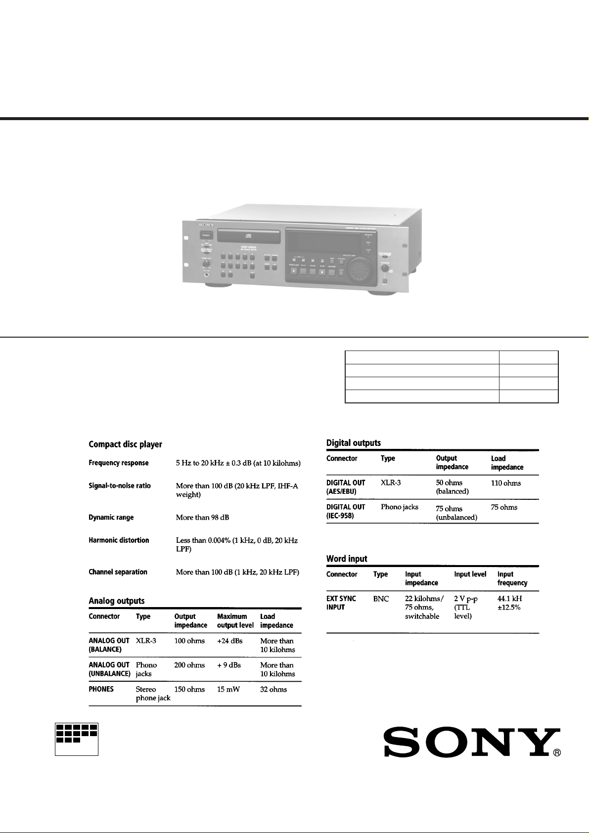
CDP-D500
US Model
Canadian Model
AEP Model
UK Model
Model Name Using Similar Mechanism NEW
CD Mechanism Type
Base Unit Name BU-5R
Optical Pick-up Name KSS-213B/K-N
CDM19G-5R
SPECIFICATIONS
– Continued on next page –
COMPACT DISC PLAYER
MICROFILM
Notes on chip component replacement
• Never reuse a disconnected chip component.
• Notice that the minus side of a tantalum capacitor may be dam-
aged by heat.
This appliance is classified as a
CLASS 1 LASER product.
The CLASS 1 LASER PRODUCT MARKING is located on the
rear exterior.
CAUTION
Use of controls or adjustments or performance of
procedures other than those specified herein may
result in hazardous radiation exposure.
SAFETY-RELATED COMPONENT WARNING!!
COMPONENTS IDENTIFIED BY MARK ! OR DOTTED
LINE WITH MARK ! ON THE SCHEMATIC DIAGRAMS
AND IN THE PARTS LIST ARE CRITICAL TO SAFE
OPERATION. REPLACE THESE COMPONENTS WITH
SONY PARTS WHOSE PART NUMBERS APPEAR AS
SHOWN IN THIS MANUAL OR IN SUPPLEMENTS PUBLISHED BY SONY.
ATTENTION AU COMPOSANT AYANT RAPPORT
LES COMPOSANTS IDENTIFIÉS P AR UNE MARQUE !
SUR LES DIAGRAMMES SCHÉMA TIQ UES ET LA LISTE
DES PIÈCES SONT CRITIQUES POUR LA SÉCURITÉ
DE FONCTIONNEMENT. NE REMPLACER CES COMPOSANTS QUE PAR DES PIÈCES SONY DONT LES
NUMÉROS SONT DONNÉS DANS CE MANUEL OU
DANS LES SUPPLÉMENTS PUBLIÉS PAR SONY.
À LA SÉCURITÉ!
– 2 –
SAFETY CHECK-OUT
After correcting the original service problem, perform the following safety check before releasing the set to the customer:
Check the antenna terminals, metal trim, “metallized” knobs, screws,
and all other exposed metal parts for AC leakage.
Check leakage as described below.
LEAKAGE TEST
The AC leakage from any exposed metal part to earth ground and
from all exposed metal parts to any exposed metal part having a
return to chassis, must not exceed 0.5 mA (500 microampers.). Leakage current can be measured by any one of three methods.
1. A commercial leakage tester, such as the Simpson 229 or RCA
WT-540A. Follow the manufacturers’ instructions to use these
instruments.
2. A battery-operated AC milliammeter. The Data Precision 245
digital multimeter is suitable for this job.
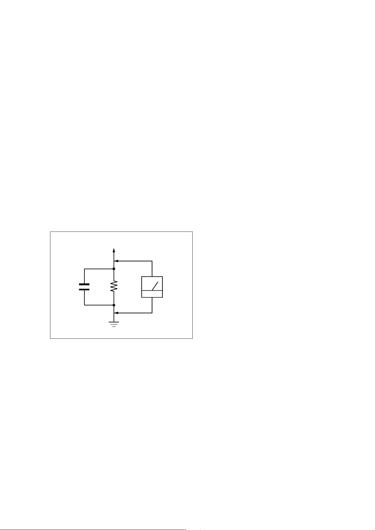
3. Measuring the voltage drop across a resistor by means of a V OM
or battery-operated A C voltmeter. The “limit” indication is 0.75
V, so analog meters must have an accurate low-voltage scale.
The Simpson 250 and Sanwa SH-63Trd are examples of a passive VOM that is suitable. Nearly all battery operated digital
multimeters that have a 2 V AC range are suitable. (See Fig. A)
TABLE OF CONTENTS
1. SERVICING NOTES
................................................... 4
2. GENERAL ..................................................................... 5
3. DISASSEMBLY............................................................ 13
4. TEST MODE ................................................................. 15
5. ELECTRICAL ADJUSTMENTS ............................ 16
6. DIAGRAMS
6-1. Block Diagram................................................................... 19
6-2. Printed Wiring Boards – CD Section –.............................. 23
6-3. Schematic Diagram – CD Section – .................................. 25
6-4. Printed Wiring Boards – Main Section – ........................... 28
6-5. Schematic Diagram – Main Section – ............................... 31
6-6. Schematic Diagram – Panel Section –............................... 36
6-7. Printed Wiring Boards – Panel Section – .......................... 41
6-8. IC Pin Function Description .............................................. 46
7. EXPLODED VIEWS ................................................... 49
To Exposed Metal
Parts on Set
AC
0.15 µF
1.5 k
Ω
Earth Ground
voltmeter
(0.75 V)
Fig. A. Using an AC voltmeter to check AC leakage.
8. ELECTRICAL PARTS LIST .................................... 54
– 3 –
SECTION 1
SERVICING NOTES
NOTES ON HANDLING THE OPTICAL PICK-UP
BLOCK OR BASE UNIT
The laser diode in the optical pick-up block may suffer electrostatic
break-down because of the potential difference generated by the
charged electrostatic load, etc. on clothing and the human body.
During repair, pay attention to electrostatic break-down and also
use the procedure in the printed matter which is included in the
repair parts.
The flexible board is easily damaged and should be handled with
care.
NOTES ON LASER DIODE EMISSION CHECK
The laser beam on this model is concentrated so as to be focused on
the disc reflective surface by the objective lens in the optical pickup block. Therefore, when checking the laser diode emission, observe from more than 30 cm away from the objective lens.
LASER DIODE AND FOCUS SEARCH OPERATION
CHECK
1. Make POWER switch on with no disc inserted and disc table
closed.
2. Confirm that the following operation is performed while observing the objective lens.
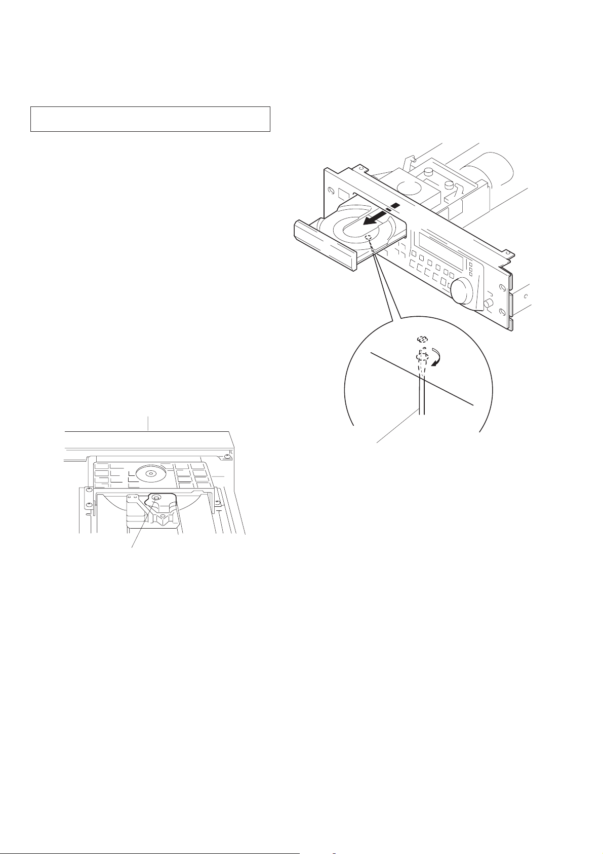
HOW T O OPEN THE DISC TRAY WHEN PO WER SWITCH
TURNS OFF
Front Panel side
1
Confirm that laser beam spread.
2
Up and down motion of the objective lens. (3 times)
Insert a tapering driver into the aperture of the unit bottom,
and turn to the direction of arrow.
* To close the disc tray, turn the driver in the reverse direction.
– 4 –
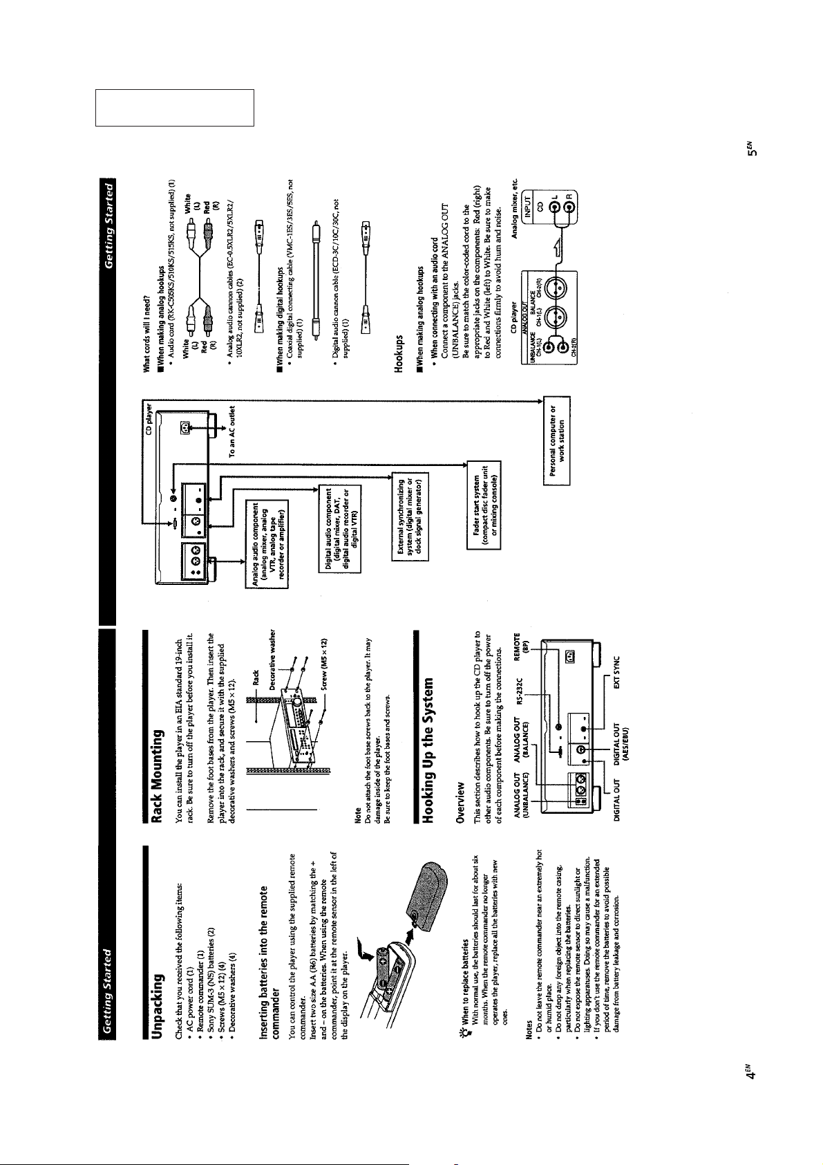
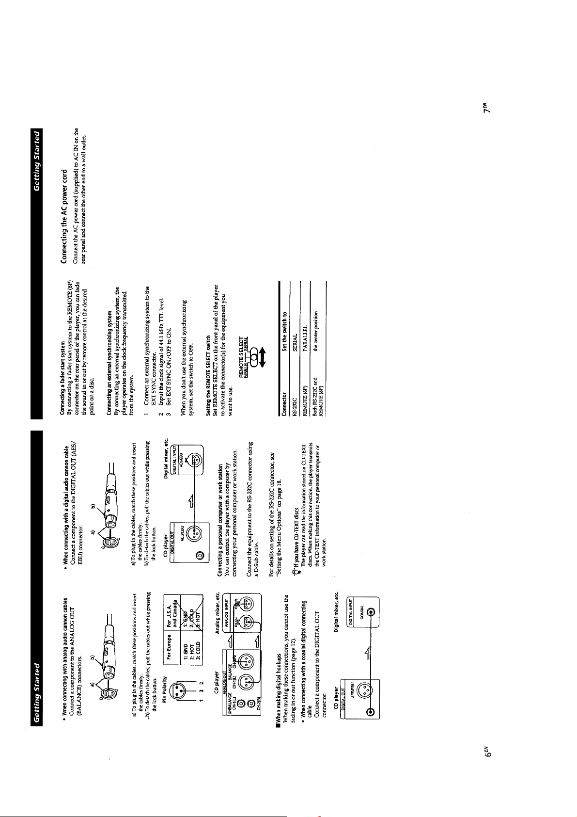
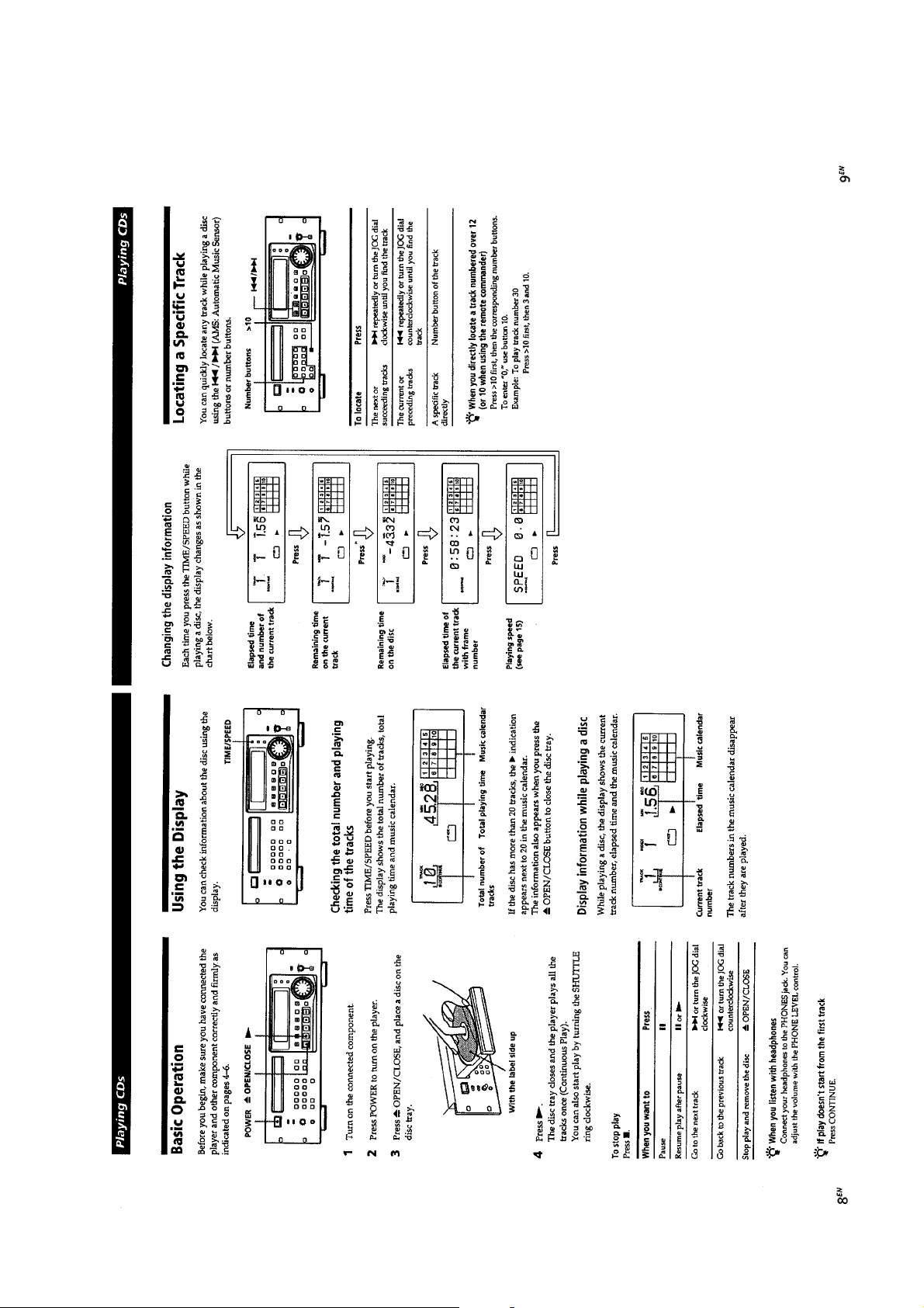
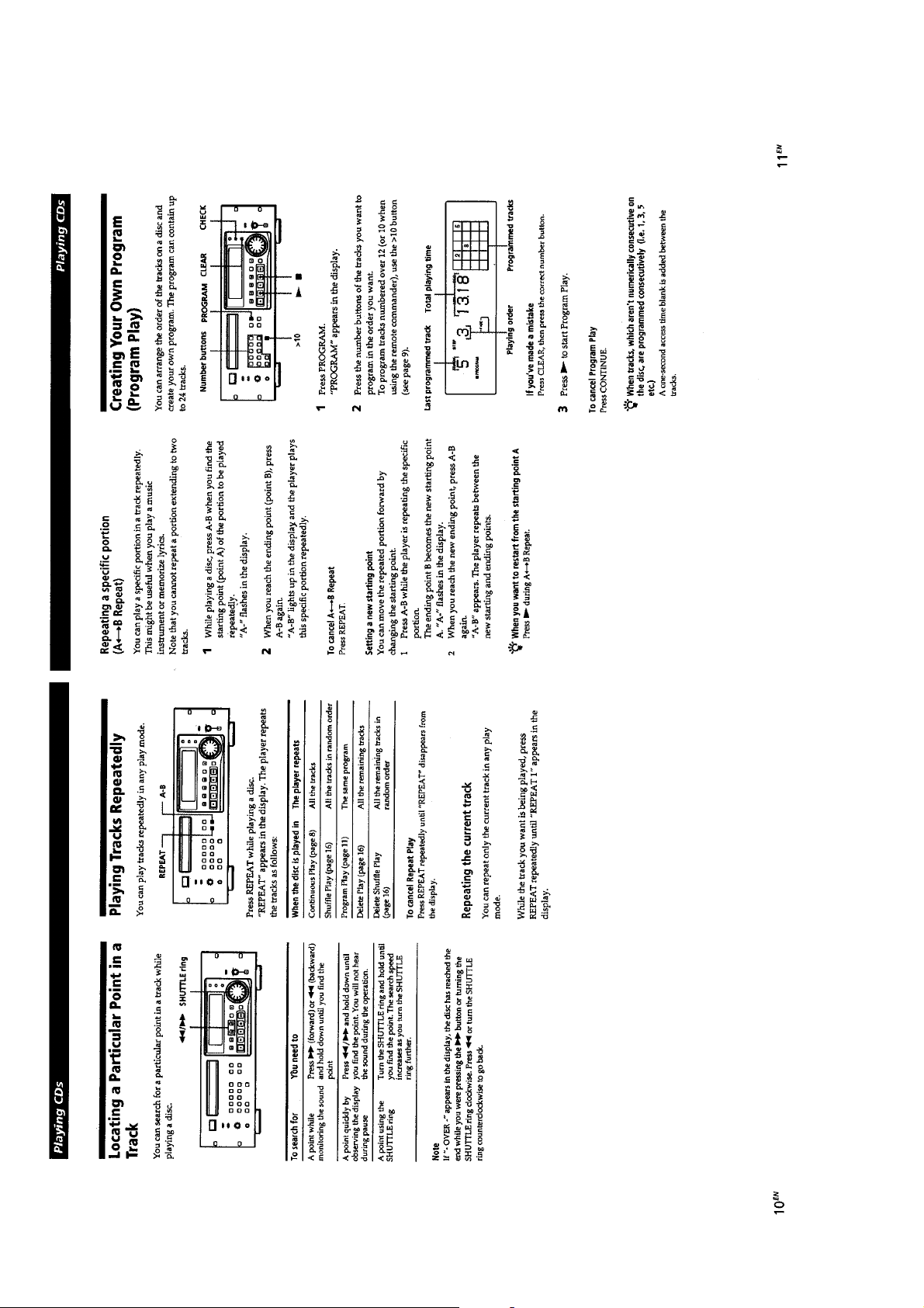
This section is extracted
from instruction manual.
SECTION 2
GENERAL
– 5 –
– 6 –
– 7 –
– 8 –
– 9 –
– 10 –
Playing CDs
– 11 –
– 12 –
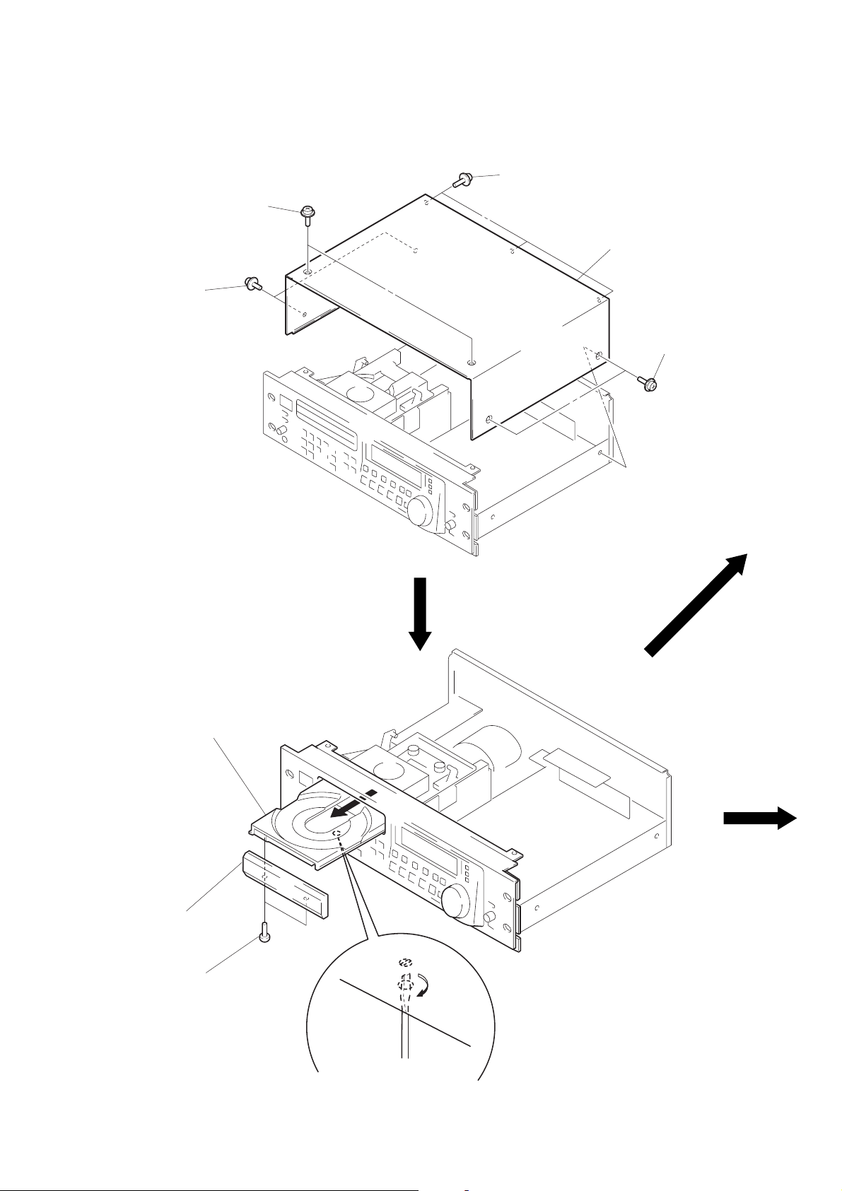
SECTION 3
DISASSEMBLY
Note: Follow the disassembly procedure in the numerical order given.
CASE
1
three screws
×
10)
(M3
1
three screws
×
10)
(M3
1
three screws
(M3
×
10)
2
case
1
two screws
(M3
×
10)
LOADING PANEL
2
Pull the disc table
4
loading panel
3
two screws
×
(BVTP3
10)
– 13 –
1
Insert a tarpering driver into the
aperture of the unit bottom,
and turn to the direction of arrow.
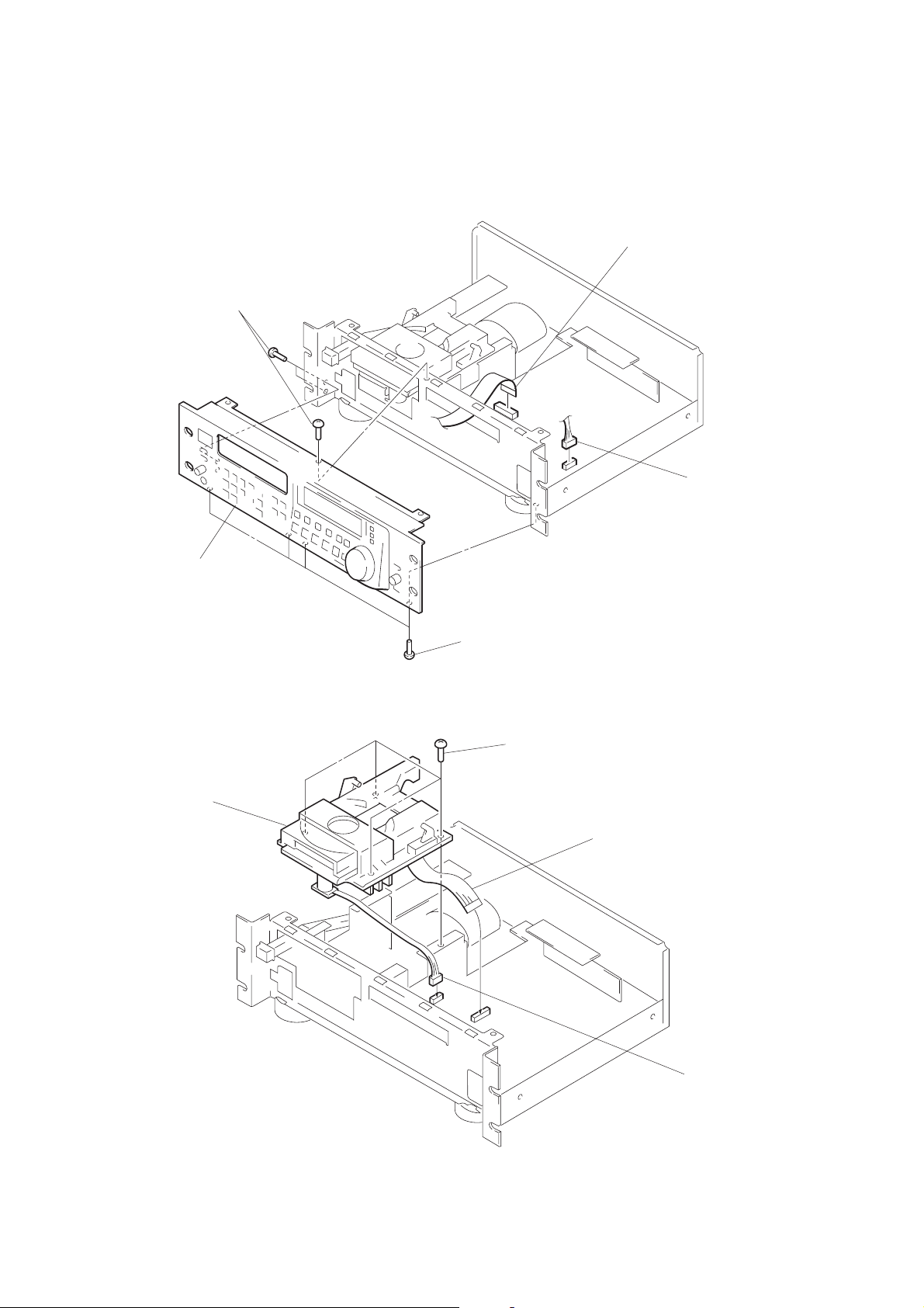
FRONT PANEL SECTION
3
4
front panel
three screws
(BVTT3
×
8)
1
flat wire (27 core)
(CN501)
2
connector
(CN331)
MECHANISM DECK
4
mechanism deck
3
four screws
(BVTT3
×
8)
3
four screws
(BVTT3
×
8)
1
flat wire (19 core)
(CN401)
2
connector
(CN531)
– 14 –
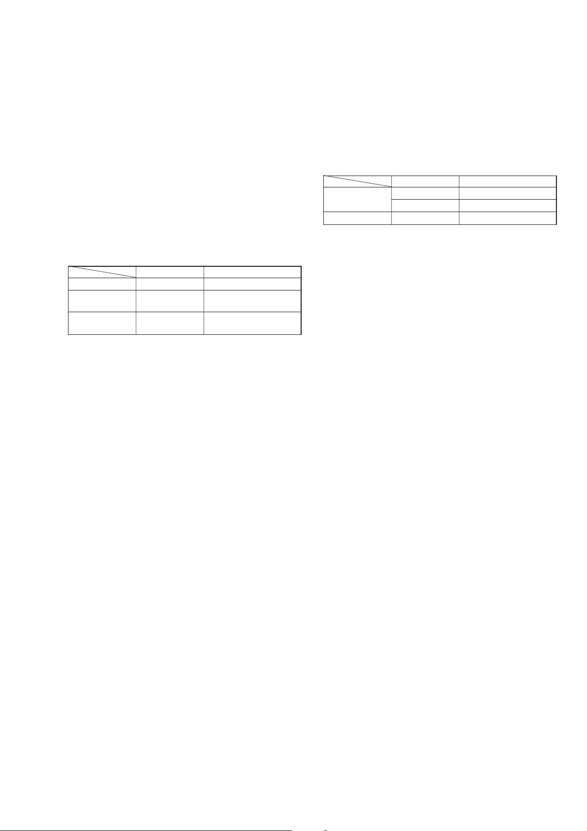
Key Check
(tact switch)
1) Connect the test point TP (ADJ) on MAIN board to the
ground with a lead wire on MAIN board.
2) Turn on the power with turning OFF the TIMER SW.
↓
“KEY TEST” shall be shown.
3) When the TA CT SW is pushed, the order of pushing is shown
on digit 0 and 1.
4) It will count up until 34 which is the maximum ke y number .
“END” will be shown after 34.
(slide switch)
Words as below shall be shown.
OFF ON
TIMER SW NULL (not shown) REPEAT
REMOTE CONTINUE/ Parallel ON → PROGRAM
SELECT SW PROGRAM Serial ON → CONTINUE
AUTO CUE/
PAUSE SW
NULL (not shown)
A.CUE ON → AUTO CUE
A.PAUSE ON → AUTO P AUSE
(JOG)
When dial the VARI SPEED JOG/AMS dial, the value on digit
6 and 7 will be clocwise/rev clockwise.
SECTION 4
TEST MODE
CXD2545 Servo Check
1) Connect the test point TP (ADJ) on MAIN board to the
2) Turn on the power, tuning ON the TIMER SW.
3) Establish as below articles with the combination of TENKEY
TIMER SW OFF 3 Tracking servo off
TIMER SW ON 1
ground with a lead wire on MAIN board.
and TIMER SW.
TENKEY MODE
8 Tracking servo on
S-cuve observe
(shuttle)
Is it turns to forward direction, calendar will show 1·2·3 and 4
and if turns to backward direction. Calendar will show 16·17·18
and 19.
EDP Bridge Check
1) Connect the test point TP (ADJ) on MAIN board to the
ground with a lead wire on MAIN board.
2) Turn on the power, with turning ON the TIMER SW.
3) Elements next to digit/segment will turn on and off mutually.
4) When both sides elements turn on at the same time the grid
is a bridge.
5) When the calendar does not work correctly, segment is a
bridge.
S-RAM Verify Check
1) Connect the test point TP (ADJ) on MAIN board to the
ground with a lead wire on MAIN board.
2) Turn on the power, with turning ON the TIMER SW and
CUE SW.
3) Address (0x8000~0x9fef) will be written by µ-com on the
digit 5 and 6, and they will be read by µ-com on the digit 8
and 9, then the value shall be shown on the digit 0 to 3.
When the written value do not agree with the read value,
“VERIFY ERROR” will be shown.
After that, it will show the position of address line and the
data line which are cause of S-RAM bridge and a float.
– 15 –
SECTION 5
ELECTRICAL ADJUSTMENTS
Note:
1. CD Block is basically designed to operate without adjustment.
Therefore, check each item in order given.
2. Use YEDS-18 disc (3-702-101-01) unless otherwise indicated.
3. Use an oscilloscope with more than 10MΩ impedance.
4. Clean the object lens by an applicator with neutral detergent
when the signal level is low than specified value with the following checks.
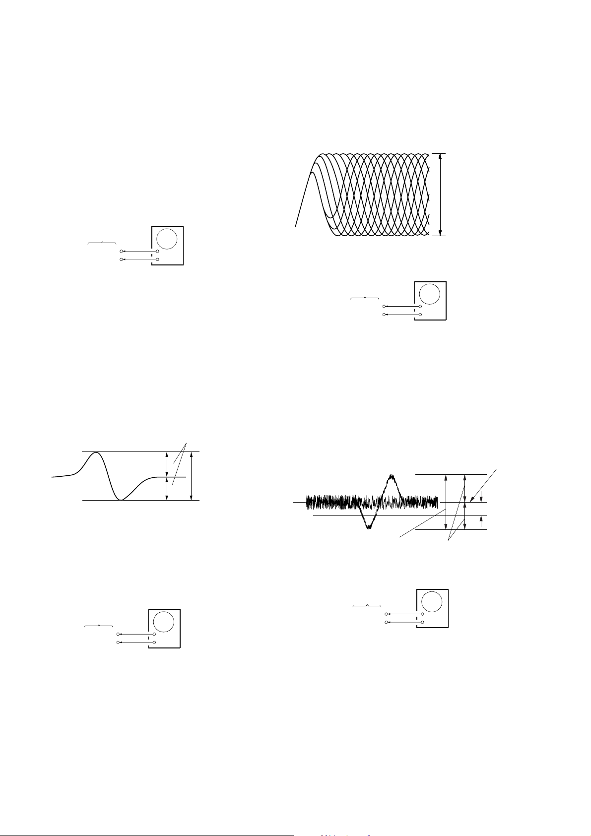
S-Curve Check
oscilloscope
BSL board
TP (FE)
TP (VC)
+
–
Procedure:
1. Connect the test point TP (ADJ) on MAIN board to the ground
with a lead wire on MAIN board.
2. Connect oscilloscope to test point TP (FE) on BSL board.
3. Turned Power switch on to set ADJ mode by TIMER SW OFF.
4. Put disc (YEDS-18) in and turned Power switch on again and
actuate the focus search. (actuate the focus search when disc
table is moving in and out.)
5. TIMER SW ON.
6. Press the “1” button (s-cuve observe mode).
7. Check the oscilloscope waveform (S-curve) is symmetrical between A and B. And confirm peak to peak level within 3 ± 1 Vp-p.
S-curve wavef orm
symmetry
A
B
within 3
±
1 Vp-p
Note: A clear RF signal waveform means that the shape “≈” can
be clearly distinguished at the center of the waveform.
RF signal waveform
VOLT/DIV: 200 mV
TIME/DIV: 500 ns
level: 1.2 Vp-p
+0.25
–0.20
E-F Balance (1 Track Jump) Check
oscilloscope
BSL board
TP (TE)
TP (VC)
+
–
Procedure:
1. Connect oscilloscope to test point TP (TE) on BSL board.
2. Turned Power switch on.
3. Put disc (YEDS-18) in to play the number five track.
4. Press the “P (Pause)” button. (Becomes the 1 track jump mode)
5. Check the level B of the oscilloscope’s waveform and the A
(DC voltage) of the center of the Travers waveform.
Confirm the following :
A/B × 100 = less than ± 6 (%)
1 track jump waveform
Center of the waveform
B
Note: • Try to measure se veral times to make sure that the ratio of
A:B or B:A is more than 10:7.
• T ake sweep time as long as possible and light up the bright-
ness to obtain best waveform.
RF Level Check
oscilloscope
BSL board
TP (RF)
TP (VC)
+
–
Procedure:
1. Connect oscilloscope to test point TP (RF) on BSL board.
2. Turned Power switch on.
3. Put disc (YEDS-18) in to play the number five track.
4. Confirm that oscilloscope waveform is clear and check RF signal level is correct or not.
0V
level : 1.5 Vp-p symmetry
+1.5
–0.5
E-F Balance Check
oscilloscope
BSL board
TP (TE)
TP (VC)
+
–
Procedure:
1. Connect the test point TP (ADJ) on MAIN board on the ground
with a lead wire on MAIN board.
2. Connect oscilloscope to test point TP (TE) on BSL board.
3. Turn the Power switch on to set the ADJ mode. (TIMER SW
OFF)
4. Put disc (YEDS-18) in to play the number five track.
5. Press the “3” button. (The tracking servo and the sledding servo
are turned OFF.)
– 16 –
A (DC voltage)
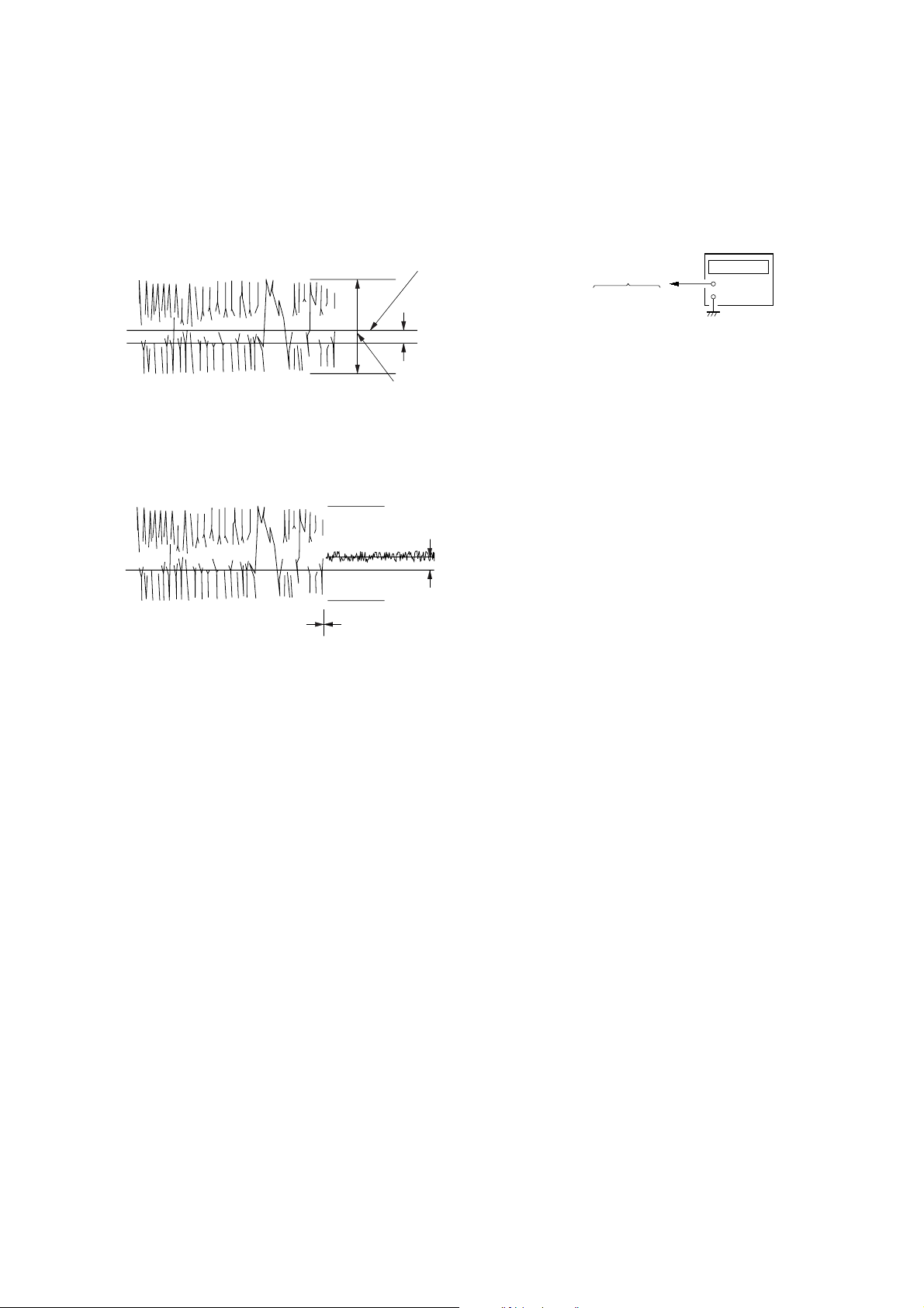
6. Check the level B of the oscilloscope’s waveform and the A
)
)
r
(DC voltage) of the center of the Traverse waveform.
Confirm the following:
A/B × 100 = less than ± 6 (%)
Traverse waveform
Center of the waveform
B
RF PLL Free-run Frequency Check
Procedure:
1. Connect frequency counter to test point (XPLCK) with a lead
wire.
frequency counte
MAIN board
TP (XPLCK)
+
–
0V
level : 1.5 Vp-p
A (DC voltage
+1.5
–0.5
7. Press the “8” button. (The tracking servo and sledding servo are
turned ON.) Confirm the C (DC voltage) is almost equal to the
A (DC voltage) is step 6.
Traverse waveform
C (DC
0V
Tracking servo
Sledding servo
OFF
Tracking servo
Sledding servo
ON
voltage
8. Disconnect the lead wire of TP (ADJ) connected in step 1.
2. Turned Power switch on.
3. Put the disc (YEDS-18) in to play the number five track.
Confirm that reading on frequency counter is 4.3218 MHz.
Balance Level Adjustment
(Generally it does not need to adjust because it has alredy adjusted
before shipping.)
1. Turn on the disc (YEDS-18) and play the number 2 track (1 kHz
0 dBs)
2. Connect level meter to BALANCE OUT (J304)
3. Adjustment level
BALANCE OUT: +24 dBs
RV101 (L-CH)
RV201 (R-CH)
– 17 –
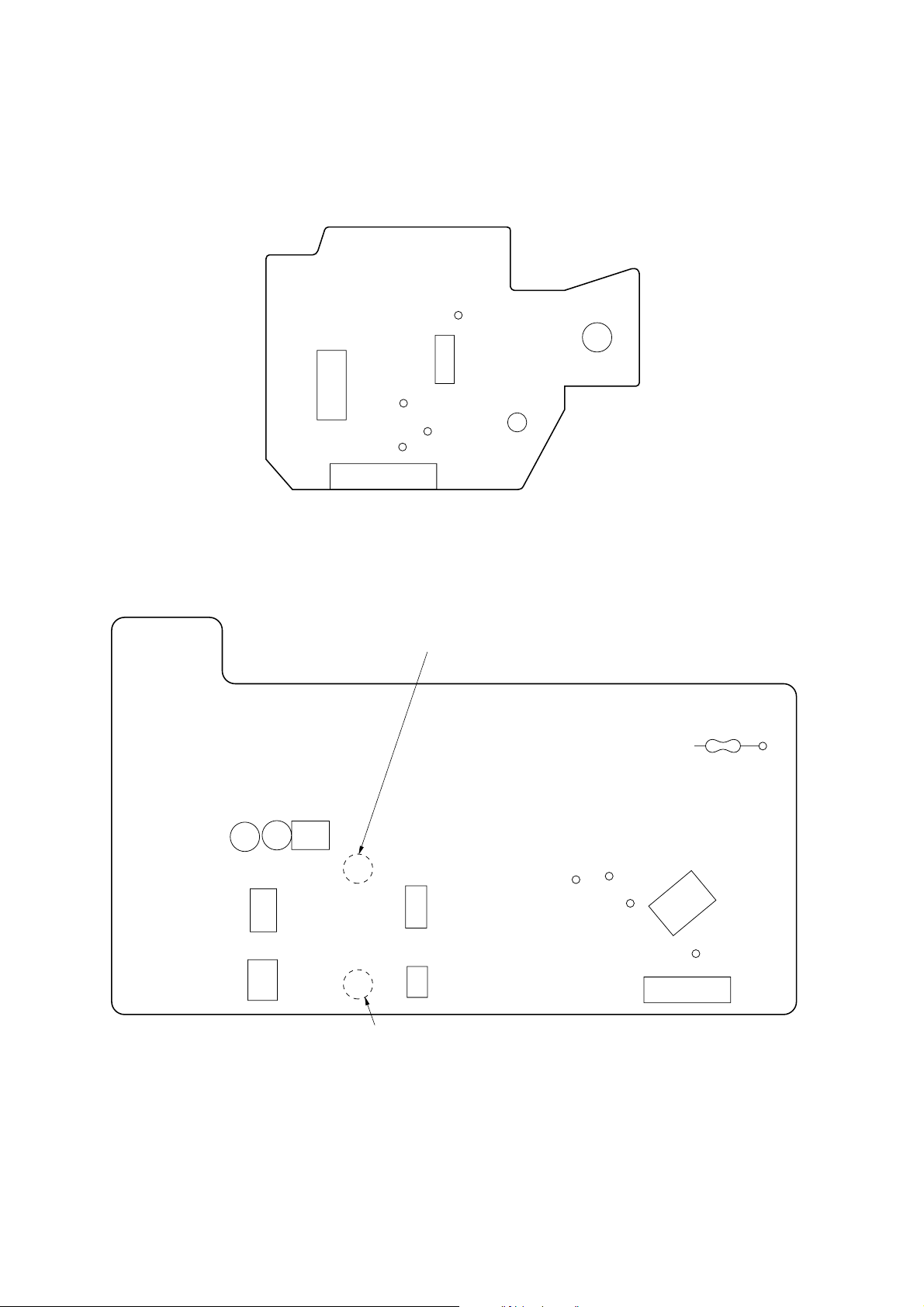
[BSL BOARD] — Side B —
[MAIN BOARD] — Component side —
IC21
CN01
TP
(VC)
TP
(RF)
TP (TE)
IC31
M102
TP
(FE)
C302
C301
IC302
IC301
IC601
RV101
BALANCE LEVEL (L-CH)
RV201
BALANCE LEVEL (R-CH)
IC304
IC303
TP
(FE1)
TP (TE1 )
TP
(VC)
R500
TP (ADJ)
IC401
TP
(XPLCK)
IC305
– 18 –
 Loading...