

SONY CDPC672A Service Manual
CD-PC672
SERVICE MANUAL
No. S4915CDPC672/
CD-PC672
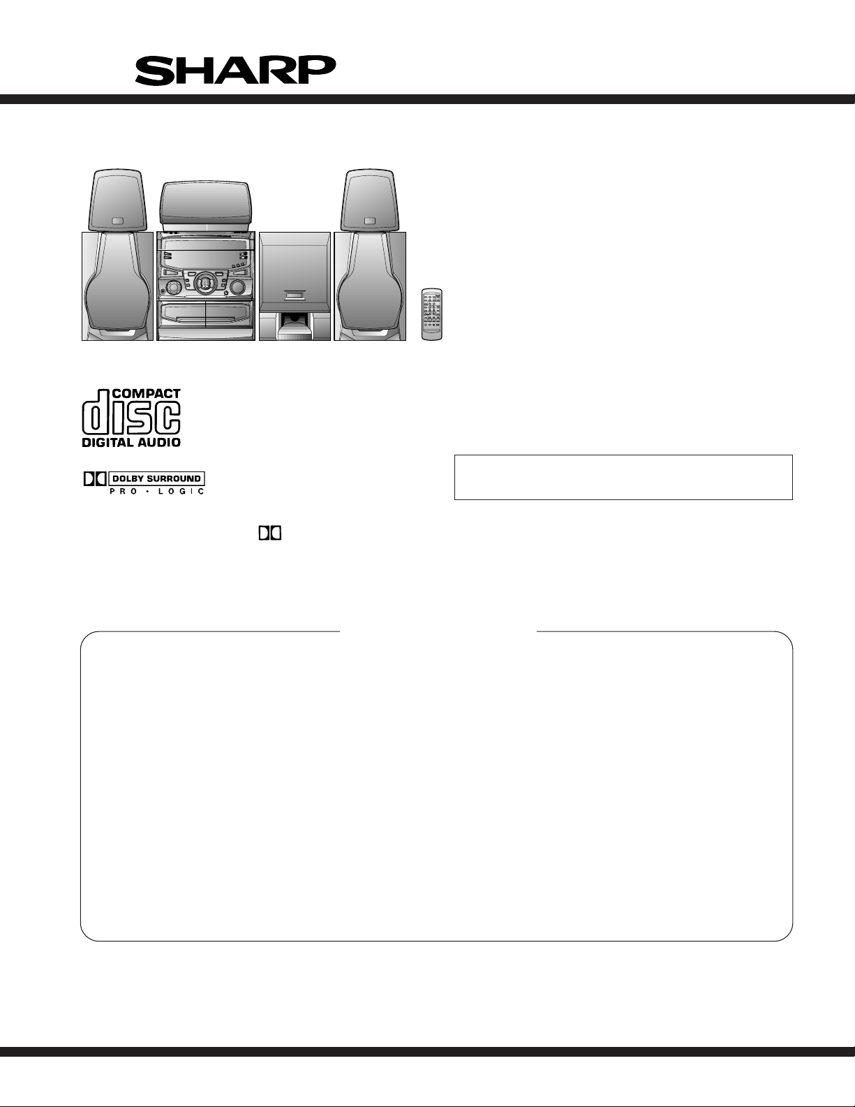
CD-PC672 mini component system consisting of CD-PC672 (main
unit), CP-C672 (front speakers), CP-SW672 (sub woofer),
GBOXS0022AWM1 (center speaker) and GBOXS0023AWM1 (rear
speaker).
• In the interests of user-safety the set should be restored to its
original condition and only parts identical to those specified be
used.
Manufactured under license from Dolby Laboratories Licensing Corporation.
DOLBY, the double-D symbol and "PRO LOGIC" are
trademarks of Dolby Laboratories Licensing Corporation.
CONTENTS
IMPORTANT SERVICE NOTES (For U.S.A. Only) ........................................................................................................... 2
SPECIFICATIONS ..............................................................................................................................................................3
NAMES OF PARTS ........................................................................................................................................................... 4
OPERATION MANUAL ...................................................................................................................................................... 7
QUICK GUIDE ................................................................................................................................................................... 8
DISASSEMBLY.................................................................................................................................................................. 9
REMOVING AND REINSTALLING THE MAIN PARTS................................................................................................... 12
ADJUSTMENT ................................................................................................................................................................. 13
NOTES ON SCHEMATIC DIAGRAM .............................................................................................................................. 16
BLOCK DIAGRAM ........................................................................................................................................................... 17
SCHEMATIC DIAGRAM / WIRING SIDE OF P.W.BOARD..............................................................................................20
VOLTAGE ........................................................................................................................................................................ 40
WAVEFORMS OF CD CIRCUIT...................................................................................................................................... 41
TROUBLESHOOTING (CD SECTION) ........................................................................................................................... 42
FUNCTION TABLE OF IC................................................................................................................................................ 47
FL DISPLAY......................................................................................................................................................................54
REPLACEMENT PARTS LIST/EXPLODED VIEW
PACKING OF THE SET (For U.S.A. Only)
Page
SHARP CORPORATION
– 1 –
This document has been published to be used
for after sales service only.
The contents are subject to change without notice.
CD-PC672
FOR A COMPLETE DESCRIPTION OF THE OPERATION OF THIS UNIT, PLEASE REFER
TO THE OPERATION MANUAL.
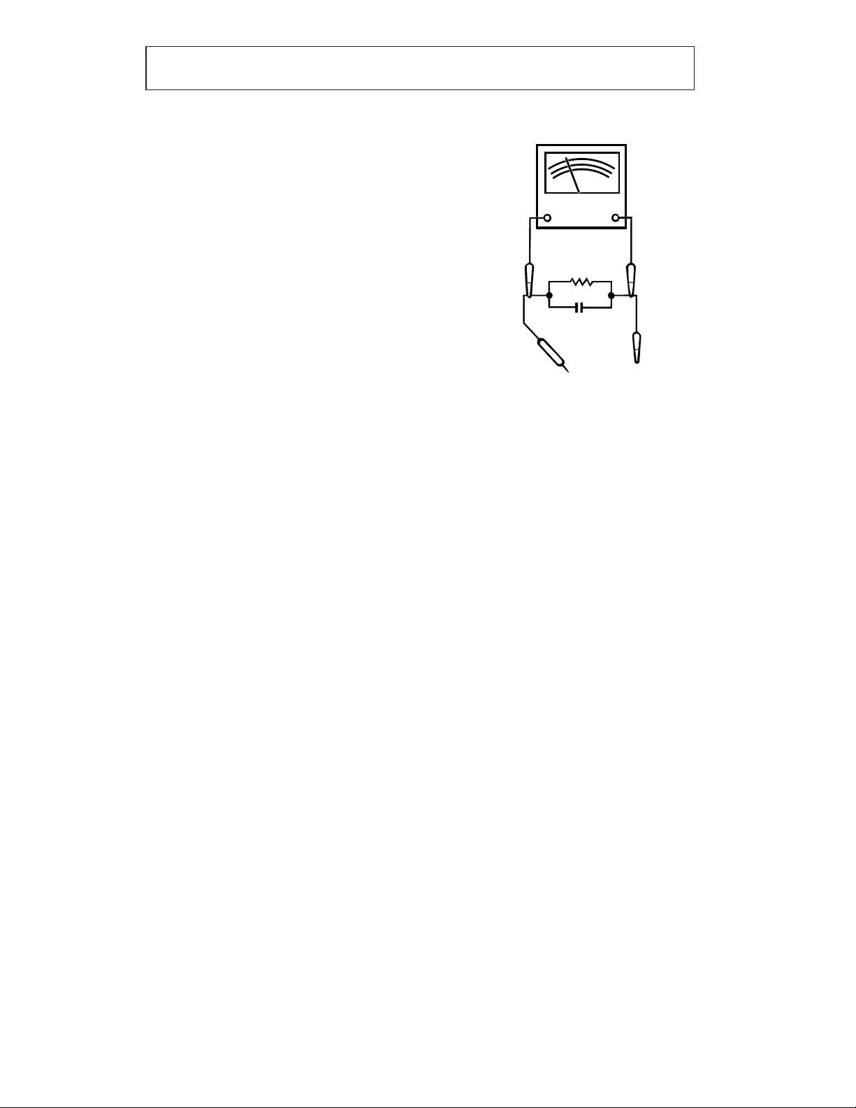
IMPORTANT SERVICE NOTES (For U.S.A. Only)
BEFORE RETURNING THE AUDIO PRODUCT
(Fire & Shock Hazard)
Before returning the audio product to the user, perform the
following safety checks.
1. Inspect all lead dress to make certain that leads are not
pinched or that hardware is not lodged between the chassis
and other metal parts in the audio product.
2. Inspect all protective devices such as insulating materials,
cabinet, terminal board, adjustment and compartment covers
or shields, mechanical insulators etc.
3. To be sure that no shock hazard exists, check for leakage
current in the following manner.
* Plug the AC line cord directly into a 120 volt AC outlet.
* Using two clip leads, connect a 1.5k ohm, 10 watt resistor
paralleled by a 0.15µF capacitor in series with all exposed
metal cabinet parts and a known earth ground, such as
conduit or electrical ground connected to earth ground.
* Use a VTVM or VOM with 1000 ohm per volt, or higher,
sensitivity to measure the AC voltage drop across the
resistor (See diagram).
* Connect the resistor connection to all exposed metal parts
having a return path to the chassis (antenna, metal cabinet,
screw heads, knobs and control shafts, escutcheon, etc.)
and measure the AC voltage drop across the resistor.
VTVM
AC SCALE
1.5k ohms
10W
0.15 µ F
TO EXPOSED
METAL PARTS
All check must be repeated with the AC line cord plug connection
reversed.
Any reading of 0.3 volt RMS (this corresponds to 0.2 milliamp.
AC.) or more is excessive and indicates a potential shock
hazard which must be corrected before returning the audio
product to the owner.
TEST PROBE
CONNECT TO
KNOWN EARTH
GROUND
– 2 –

SPECIFICATIONS
CD-PC672
General
Power source: AC 120 V, 60 Hz
Power consumption: Stand-by; 0.3 W
Power on; 150 W
Dimensions: Width; 10-5/8" (270 mm)
Height; 11-13/16" (300 mm)
Depth; 14-1/4" (362 mm)
Weight: 17.7 lbs. (8.1 kg)
Amplifier section
Output power: Front speakers; 40 W minimum
(Except for Canada) RMS into 6 ohms from 60 Hz to
20 kHz with no more than 10 %
total harmonic distortion.
Output power: Front speakers;
(For Canada) RMS; 80 W (40 W + 40 W)
(10 % T.H.D.)
Center speaker;
RMS; 20 W (10 % T.H.D.)
Rear speaker;
RMS; 20 W (total)
(10 % T.H.D.)
Sub woofer;
RMS; 40 W
(80 Hz 10 % T.H.D.)
Output terminals: Front speakers; 6 ohms
Center speaker; 4 ohms
Rear speaker; 8 ohms
Sub woofer; 6 ohms
Headphones; 16-50 ohms
(recommended; 32 ohms)
CD digital output (optical)
Input terminal: Video/Auxiliary (audio signal);
× 2; 500 mV/47 kohms
Tuner section
Frequency range: FM; 87.5 - 108 MHz
AM; 530 - 1,720 kHz
Cassette deck section
Frequency response: 50 - 14,000 Hz (Normal tape)
Signal/noise ratio: 55 dB (TAPE 1, playback)
50 dB (TAPE 2, recording/
playback)
Wow and flutter: 0.15 % (WRMS)
Compact disc player section
Type: 3-disc multi-play compact disc
player
Signal readout: Non-contact, 3-beam semi-
conductor laser pickup
D/A Converter: 1-bit D/A converter
Frequency response: 20 - 20,000 Hz
Dynamic range: 90 dB (1 kHz)
CD-PC672
Front speaker section
CP-C672
Type: 2-way 5-1/4" (13 cm) woofer
and 2" (5 cm) tweeter type
Maximum input power: 80 W
Rated input power: 40 W
Impedance: 6 ohms
Dimensions: Width; 7-7/8" (200 mm)
Height; 11-13/16" (300 mm)
Depth; 9-7/16" (240 mm)
Weight: 6.3 lbs. (2.9 kg)/each
Center speaker section
GBOXS0022AWM1
Type: 4" (10 cm) full-range speaker
Maximum input power: 40 W
Rated input power: 20 W
Impedance: 4 ohms
Dimensions: Width; 10-1/4" (260 mm)
Height; 5-1/2" (140 mm)
Depth; 6-1/8" (155 mm)
Weight: 2.0 lbs. (0.9 kg)/each
Rear speaker section
GBOXS0023AWM1
Type: 4" (10 cm) full-range speaker
Maximum input power: 20 W
Rated input power: 10 W
Impedance: 8 ohms
Dimensions: Width; 6-3/4" (170 mm)
Height; 3-1/2" (88 mm)
Depth; 6-3/4" (170 mm)
Weight: 1.0 lbs. (0.5 kg)/each
Sub woofer section
CP-SW672
Type: 5-1/4" (13 cm) full-range
speaker
Maximum input power: 80 W
Rated input power: 40 W
Impedance: 6 ohms
Dimensions: Width; 7-7/8" (200 mm)
Height; 11-13/16" (300 mm)
Depth; 11-5/8" (295 mm)
Weight: 7.5 lbs. (3.4 kg)/each
Specifications for this model are subject to change without
prior notice.
– 3 –
1
3
4
2
5
6
7
8
9
10
11
12
13
16
17
14
15
18
19 20 213522
25
27
29
26
30
37
31
32
33
34 36
38
39
23
24
28
41
40
CD-PC672
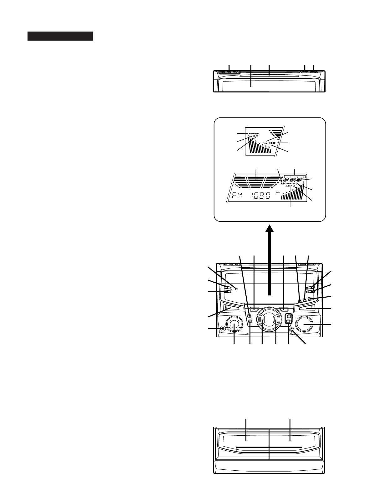
NAMES OF PARTS
CD-PC672
■ Front panel
11. Disc Number Selector Buttons
12. Disc Tray
13. Multi Indicator
14. Disc Skip Button
15. Open/Close Button
16. Extra Bass Indicator
17. FM Stereo Mode Indicator
18. FM Stereo Indicator
19. (CD) Repeat Indicator
10. (CD) Play Indicator
11. (CD) Pause Indicator
12. Spectrum Analyzer/Volume Level Indicator
13. (TAPE 2) Record Indicator
14. (CD) Disc Number Indicators
15. (CD/TUNER) Memory Indicator
16. Timer Play Indicator
17. Timer Record Indicator
18. Sleep Indicator
19. (TAPE 2) Record Pause Button
20. (CD) Track Down/Review Button
3 (TUNER) Preset Down Button
3 (TAPE 2) Rewind Button
21. (CD) Track Up/Cue Button
3 (TUNER) Preset Up Button
3 (TAPE 2) Fast Forward Button
22. Bypass Button
23. Normal Button
24. Timer Set Indicator
25. Timer/Sleep Button
26. Clock Button
27. Power Button
28. Headphone Socket
29. Equalizer Mode Selector Button
30. Dimmer Button
31. Phantom Button
32. Extra Bass/Demo Mode Button
33. Volume Control
34. Function Selector Buttons
35. Memory/Set Button
36. (CD/TAPE) Stop Button
37. (TAPE) Play Button
3 (CD) Play/Repeat Button
38. Tuning and Time Up/Down Buttons
39. Sub Woofer Volume Control
40. (TAPE 1) Cassette Compartment
41. (TAPE 2) Cassette Compartment
– 4 –
3
2
1
4
5
67
8
1
2
3
4
9
10
11
5
6
7
8
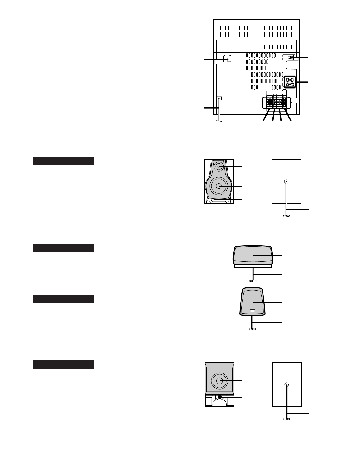
■ Rear panel
11.
CD Digital Output Socket
12.
AC Power Lead
13.
FM/AM Loop Aerial Socket
14.
Video/Auxiliary (Audio Signal) Input Sockets
15.
Rear Speaker Terminals
16.
Centre Speaker Terminals
17.
Front Speaker Terminals
18.
Sub Woofer Terminals
CD-PC672
CP-C672
■ Front speakers
11.
Tweeter
12.
Woofer
13.
Bass Reflex Duct
14.
Speaker Wire
GBOXS0022AWM1
■ Centre speaker
15.
Full-Range Speaker
16.
Speaker Wire
GBOXS0023AWM1
■ Rear speaker
17.
Full-Range Speaker
18.
Speaker Wire
CP-SW672
■ Sub woofer
19.
Woofer
10.
Bass Reflex Duct
11.
Speaker Wire
– 5 –
CD-PC672
CD-PC672
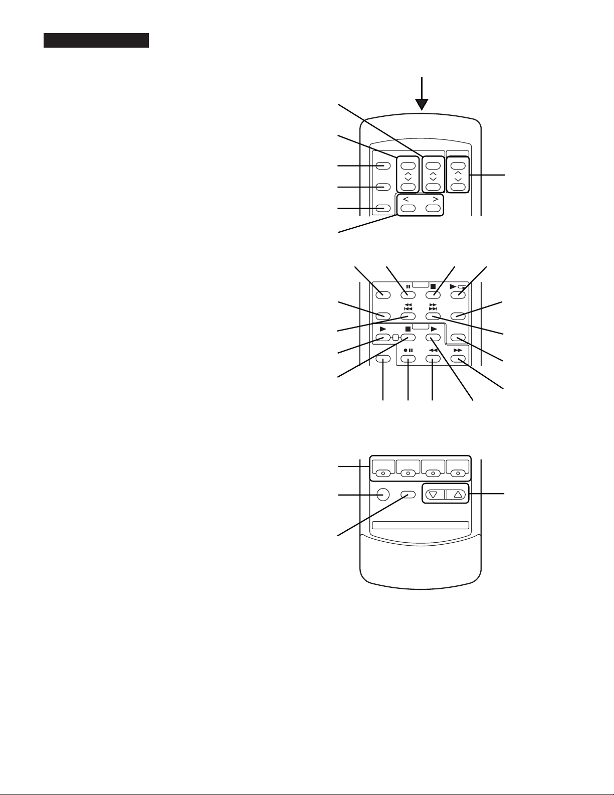
■ Remote control
11.
Remote Control Transmitter LED
12.
Surround Level Buttons
13.
Centre Level Buttons
14.
Dolby Pro Logic Button
15.
Centre Mode Button
16.
Test Tone Button
17.
Balance Control Buttons
● Tuner control section
18.
Preset Up/Down Buttons
● CD control section
19.
Memory Button
10.
Pause Button
11.
Stop Button
12.
Play/Repeat Button
13.
Clear Button
14.
Track Down/Review Button
15.
Random Button
16.
Track Up/Cue Button
17.
Disc Skip Button
2
3
4
5
6
7
13
14
18
1
109
2419202221
8
11 12
15
16
17
23
● Tape control section
18.
(TAPE 1) Play Button
19.
(TAPE 1/2) Stop Button
20.
(TAPE 2) Record Pause Button
21.
(TAPE 2) Rewind Button
22.
(TAPE 2) Play Button
23.
(TAPE 2) Fast Forward Button
24.
Equalizer Mode Button
25.
Function Selector Buttons
26.
Power Button
27.
Extra Bass Button
28.
Volume Up/Down Buttons
25
26
27
28
– 6 –
OPERATION MANUAL
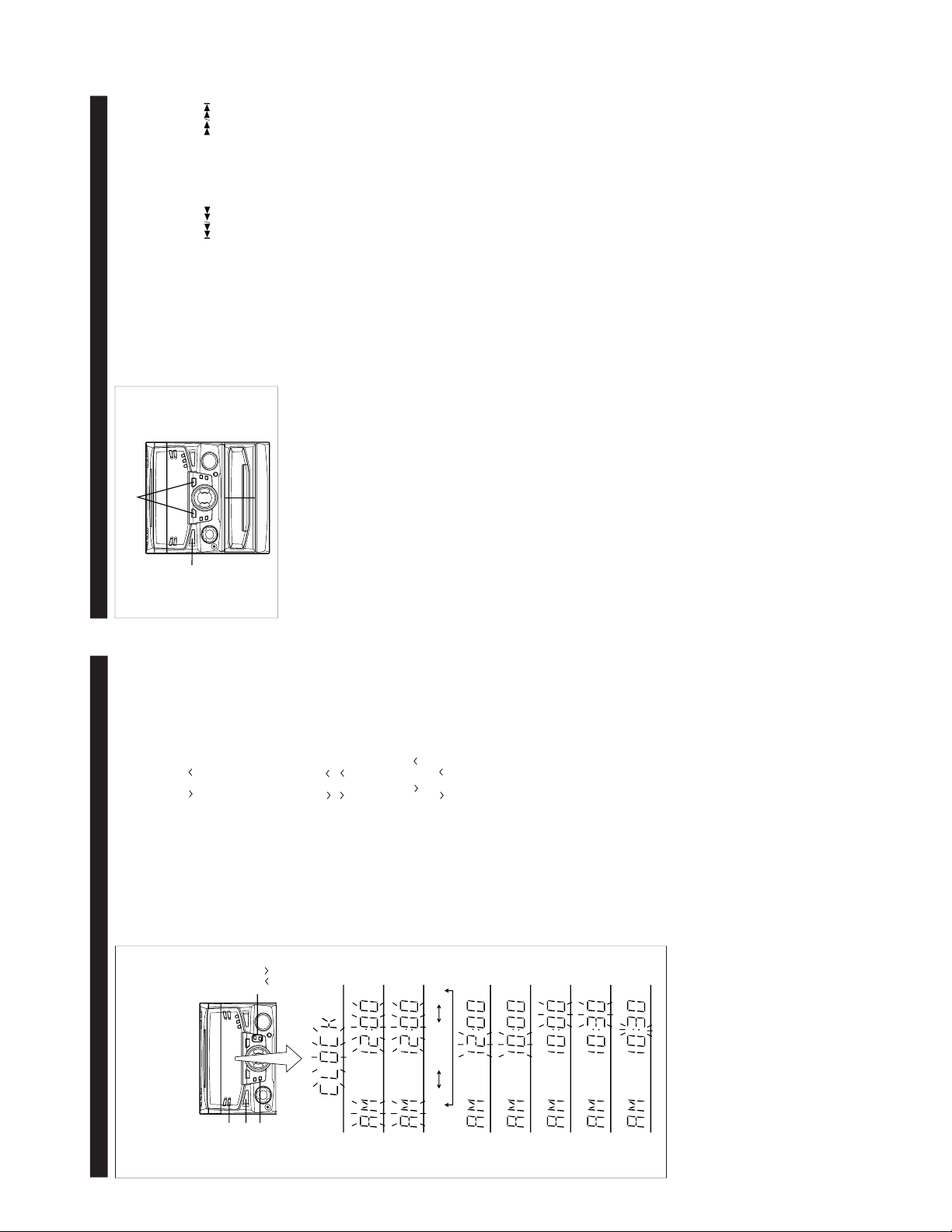
SETTING THE CLOCK
1
Press the POWER button to enter the stand-by mode.
2
Press the CLOCK button.
3
Within 5 seconds, press the MEMORY/SET button.
4
Press the TUNING/TIME ( or ) button to select the time
display mode.
"AM 12:00" → The 12-hour display will appear.
(AM 12:00 - PM 11:59)
"AM 0:00 " → The 12-hou r display will appear.
(AM 0:00 - PM 11:59)
"0:00" → T he 24-hour d isplay wil l appear.
(0:00 - 23:59)
● Note that this can only be set when the unit is first installed
or it has been reset (see page 18).
5
Press the MEMORY/SET button.
6
Press the TUNING/TIME ( or ) button to adjust the hour.
● Press the TUNING/TIME ( or ) button once to advance
the time by 1 hour. Hold it down to advance continuously.
● When the 12-hour display is selected, "AM" will change auto-
matically to "PM".
7
Press the MEMORY/SET button.
8
Press the TUNING/TIME ( or ) button to adjust the
minutes.
● Press the TUNING/TIME ( or ) button once to advance
the time by 1 minute. Hold it down to change the time in 5
minute intervals.
● The hour setting will not advance even if minutes advance from
"59" to "00".
9
Press the MEMORY/SET button.
● The clock starts operating from "0" seconds. (Seconds are not
displayed.)
Note:
● In the event of a power failure or when the AC power cord is
disconnected, the clock display will go out.
When the AC power supply is restored, the clock display will
flash on and off to indicate the time when the power failure
occurred or when the AC power cord was disconnected.
CLOCK
POWER
MEMORY/
SET
TUNING/
TIME
( )
AM 12:00 AM 0:00 0:00
2
3
4
7
6
5
8
9
If this happens, follow the procedure below to change the clock
time.
To change the clock time:
①
Press the CLOCK button.
②
Within 5 seconds, press the MEMORY/SET button.
③
Perform steps 6 - 9 above.
To see the time display:
Press the CLOCK button.
● The time display will appear for about 5 seconds.
To change the time display mode:
①
Perform steps 1 - 2 in the section "RESETTING THE MICRO-
COMPUTER", on page 18.
②
Perform steps 1 - 9 above.
(Main unit operation)
In this example, the clock is set for the
12-hour (AM 12:00) system.
RESETTING THE MICROCOMPUTER
Reset the microcomputer under the following conditions:
● To erase all of the stored memory contents (clock and timer
settings, and tuner and CD presets).
● If the display is not correct.
● If the operation is not correct.
1
Press the POWER button to enter the stand-by mode.
2
While pressing down the button and the
button, hold down the POWER button for at least 1 second.
Caution:
● The operation explained above will erase all data stored in
memory including clock and timer settings, and tuner and CD
presets.
2
1,2
CD-PC672
– 7 –
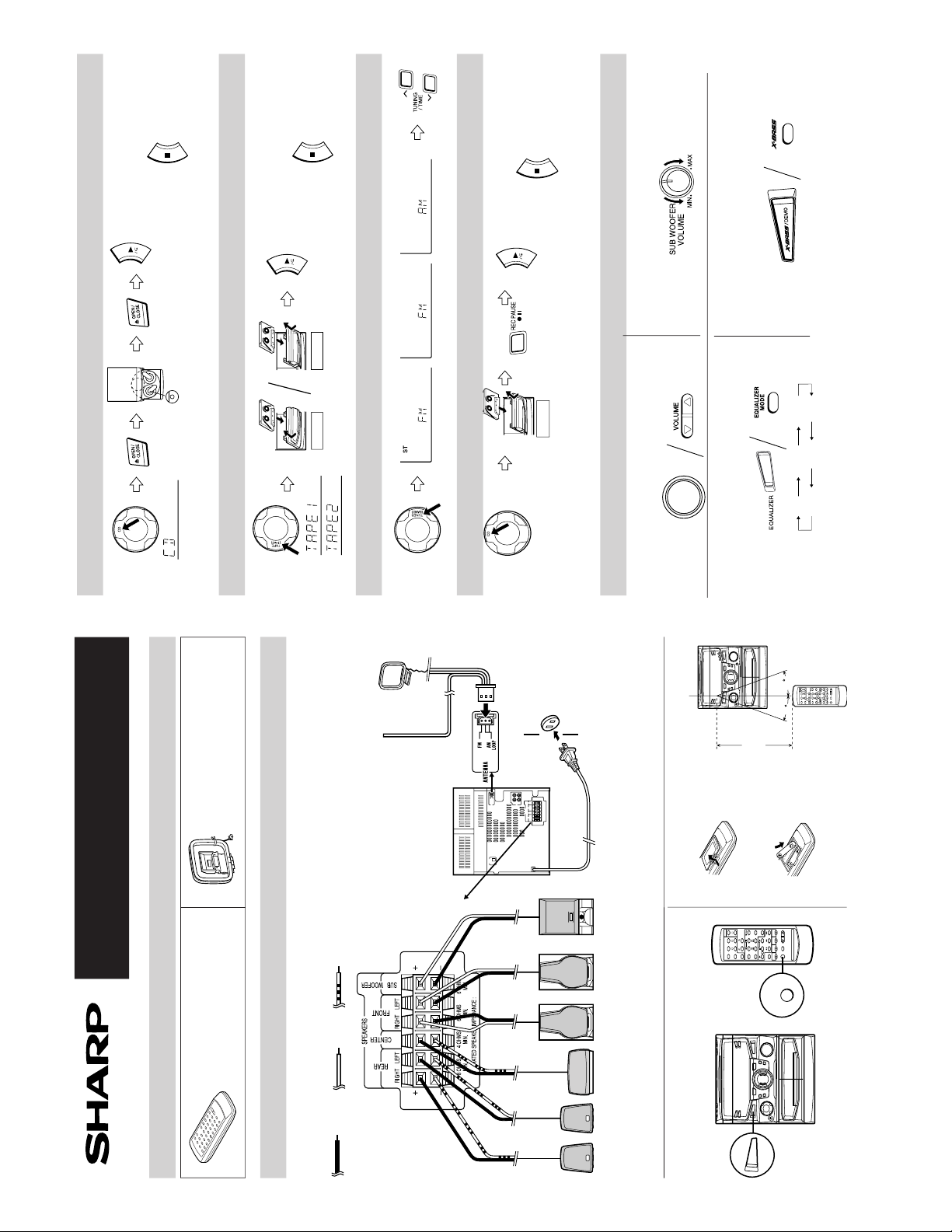
CD-PC672
MINI COMPONENT SYSTEM
Quick Guide/Guía rápida
CD-PC672
● Remote control x 1
●
Controlador remoto x 1
● 2 “AA” batteries
●
Dos pilas “AA”
Remote Sensor
Sensor remoto
2
Preparation for use /
Preparación para su uso
1
Check the supplied accessories /
Compruebe los accesorios suministrados
● FM/AM loop antenna x 1
●
Antena de cuadro de
FM/AM x 1
● Batteries are not included.
●
Las pilas no están incluidas.
8” - 20’ (0.2m - 6m)
0,2m - 6m
■ Speaker connection
■
Conexión de los altavoces
■ Antenna connection
■
Conexión de las antenas
Rear
speaker
(Right)
Altavoz
trasero
(Derecho)
Rear
speaker
(Left)
Altavoz
trasero
(Izquierdo)
Front
speaker
(Right)
Altavoz
delantero
(Derecho)
Front
speaker
(Left)
Altavoz
delantero
(Izquierdo)
● AM Loop Antenna
●
Antena de cuadro
de AM
● FM Antenna
●
Antena de FM
● AC 120 V, 60 Hz
●
120 V de CA, 60 Hz
White line
Línea blanca
Red
Rojo
Center
speaker
Altavoz
central
■ Turning the power on and off
■
Conexión y desconexión de la alimentación
■ Remote control
■
Controlador remoto
POWER
POWER
15
15
Black
Negro
Sub
woofer
Altavoz de
subgraves
3
Listening to a CD /
Audición de discos CD
4
Listening to a tape /
Audición de una cinta
5
Listening to the radio /
Audición de la radio
6
Recording from CDs /
Grabaciones de discos CD
7
Sound control /
Control del sonldo
● Label facing up
●
Etiqueta hacia arriba
■ To stop the playback
■
Para detener la reproducción
■ To stop the playback
■
Para detener la reproducción
● Load the disc to be
recorded.
●
Introduzca el disco
que va a grabar.
● CD recording
starts.
●
La grabación de
CD empieza.
■ Volume
■
Volumen
■ Extra bass (X-BASS)
■
Graves extra (X-BASS)
■ Pre-programmed equalizer
■
Ecualizador preprogramado
VOLUME
FLAT
HEAVY-1 HEAVY-2
SOFT-2
SOFT-1 VOCAL
■ To stop the playback
■
Para detener la reproducción
TAPE 1
TAPE 2
TAPE 2
■ Sub woofer volume
■
Volumen de subgraves
– 8 –
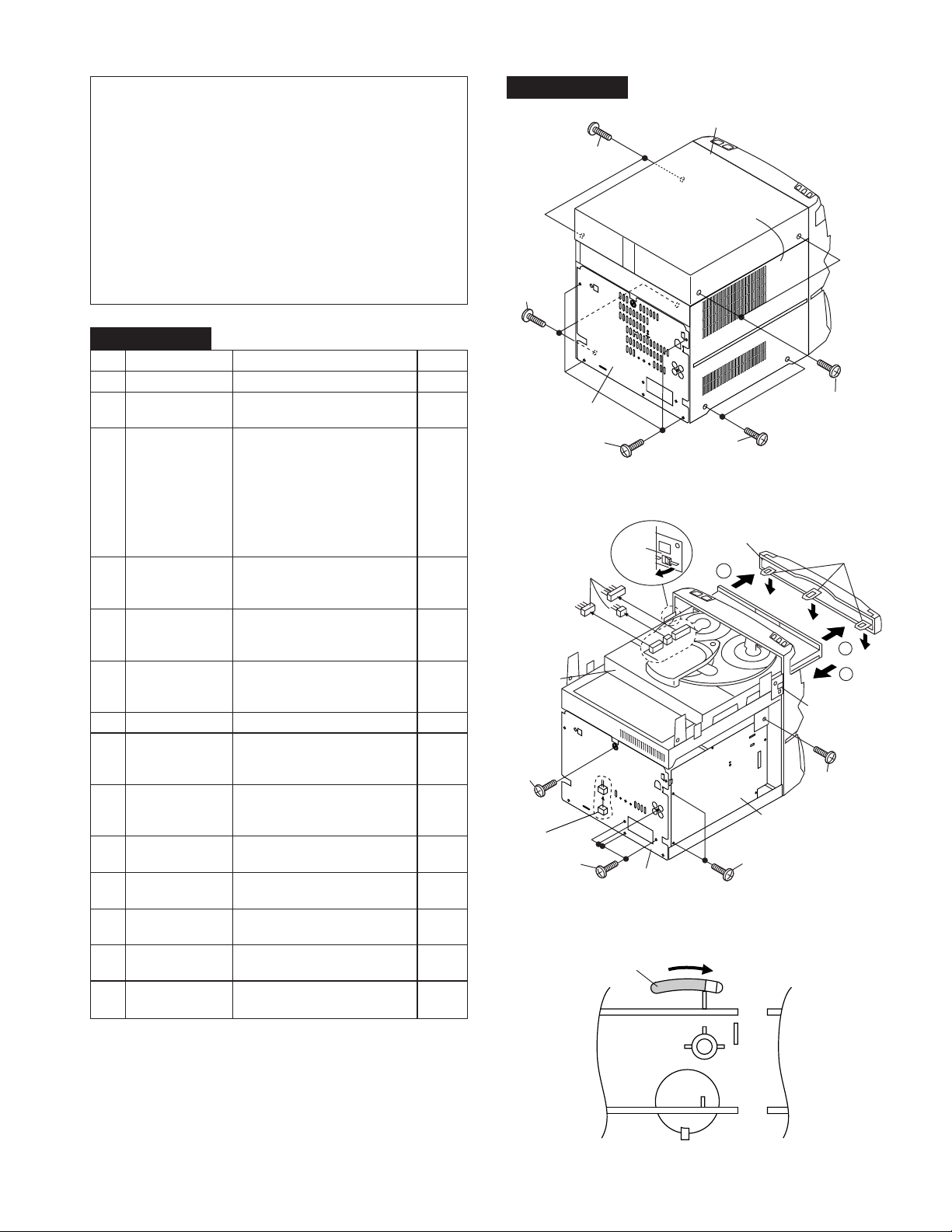
Caution on Disassembly
Top Cabinet
(A1)x2
ø3x12mm
(A1)x2
ø3x12mm
Side Panel
(Left)
(B1)x2
ø3x8mm
(B1)x2
ø3x10mm
(B1)x4
ø3x10mm
Back Board
Follow the below-mentioned notes when disassembling
the unit and reassembling it, to keep it safe and ensure
excellent performance:
1. Take cassette tape and compact disc out of the unit.
2. Be sure to remove the power supply plug from the wall
outlet before starting to disassemble the unit.
3. Take off nylon bands or wire holders where they need to
be removed when disassembling the unit. After servicing
the unit, be sure to rearrange the leads where they were
before disassembling.
4. Take sufficient care on static electricity of integrated
circuits and other circuits when servicing.
CD-PC672
STEP R EMOVAL PROCEDURE FIGURE
1 Top Cabinet 1. Screw ..................... (A1) x4 9-1
2 Side Panel 1. Screw ..................... (B1) x8 9-1
(Left/right)
3 CD Player Unit/ 1. Turn on the power supply, 9-2
CD Tray Cover open the disc tray, take out
the CD cover, and close.
(Note 1)
2. Hook....................... (C1) x3
3. Hook....................... (C2) x2
4. Socket .................... (C3) x3
5. Screw ..................... (C4) x2
4 Back Board 1. Screw..................... (D1) x6 9-2
(with Digital 2. Socket .................... (D2) x1
Output PWB)
5 Main PWB 1. Socket .................... (E1) x2 10-1
2. Flat Cable............... (E2) x1
3. Flat Wire................. (E3) x1
6 Power PWB 1. Screw ..................... (F1) x4 10-1
7 Front Panel 1. Screw ..................... (G1) x2 10-1
8 Display PWB/ 1. Screw ..................... (H1) x13 10-2
Switch PWB
Headphones PWB
9 Tape Mechanism 1. Open the cassette holder. 10-2
10 Turntable 1. Screw ..................... (K1) x1 10-3
11 Disc Tray 1. Screw ..................... (L1) x2 10-3
12 CD Servo PWB 1. Screw ..................... (M1) x1 10-4
(Note 2) 2. Socket .................... (M2) x4
13 CD Changer 1. Screw ..................... (N1) x4 10-5
Mechanism
14 CD Mechanism 1. Screw ..................... (P1) x1 10-5
2. Socket .................... (F2) x4
3. Holder PWB ........... (F3) x5
2.
Support Bracket ..... (H2) x1
2. Screw...................... (J1) x6
3. Socket .................... (J2) x1
2. Cover ..................... (K2) x1
2. Guide ..................... (L2) x2
DISASSEMBLY
CD-PC672
CD Player
Unit
(C4) x1
ø3x10mm
(D2)x1
(D1)x4
ø3x10mm
(C3) x3
LOCK
LEVER
(C2) x1
Pull
Back Board
Figure 9-1
Figure 9-2
CD Tray Cover
1
Main PWB
(D1)x2
ø3x10mm
CD-PC672
Hook
( C1) x3
1
2
(C2) x1
(C4) x1
Note 1:
How to open the changer manually. (Fig. 9-3)
1. Change, turn fully the lock lever in the arrow direction
through the hole on the loading chassis bottom in this state.
After that, push forward the CD player base.
Note 2:
1. After removing the connector for the optical pickup from the
connector, wrap the conductive aluminium foil around the
front end of connector to protect the optical pickup from
electrostatic damage.
Figure 9-3
– 9 –
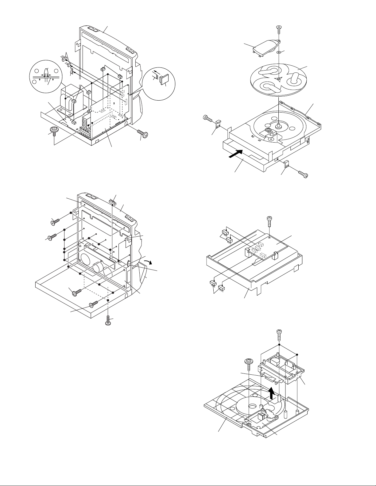
CD-PC672
(F3)x5
1 1
Push
2
Pull
POWER
PWB
POWER PWB
(F1)x3
ø3x10mm
Switch PWB
(H1)x2
ø3x10mm
(E1)x2
Push
(E2)x1
(F2)x2
Figure 10-1
Front Panel
(F2)x2
Main PWB
(J2)x1
(F1)x1
ø3x10mm
Front Panel
(E3)x1
Headphoens
PWB
( L1 ) x1
ø3 x10mm
( L2 ) x1
CD Player Unit
( K1 ) x1
ø3 x10mm
( K2 ) x1
Washer
Turntable
Disc Tray
( L1 ) x1
ø3 x10mm
( L2 ) x1
Figure 10-3
( M1 ) x1
ø3 x10mm
(H1)x10
ø3x10mm
(H1)x1
ø3x10mm
(J1)x6
ø3x10mm
Figure 10-2
(G1)x2
ø3x10mm
Display PWB
Headphones
PWB
Open
(H2)x1
Cassette
Holder
Tape Mechanism
( M2 ) x2
CD Servo PWB
( M2 ) x2
CD Player Unit
Figure 10-4
( N1 ) x4
ø3 x12mm
( P1 ) x1
ø2.6 x10mm
Shift Lever
CD Changer
Mechanism
CD Player Base
CD Mechanism
Be careful when installing the CD changer mechanism.
Install the CD changer mechanism on the CD player base after
the shift lever has been set in the highest position.
Figure 10-5
– 10 –
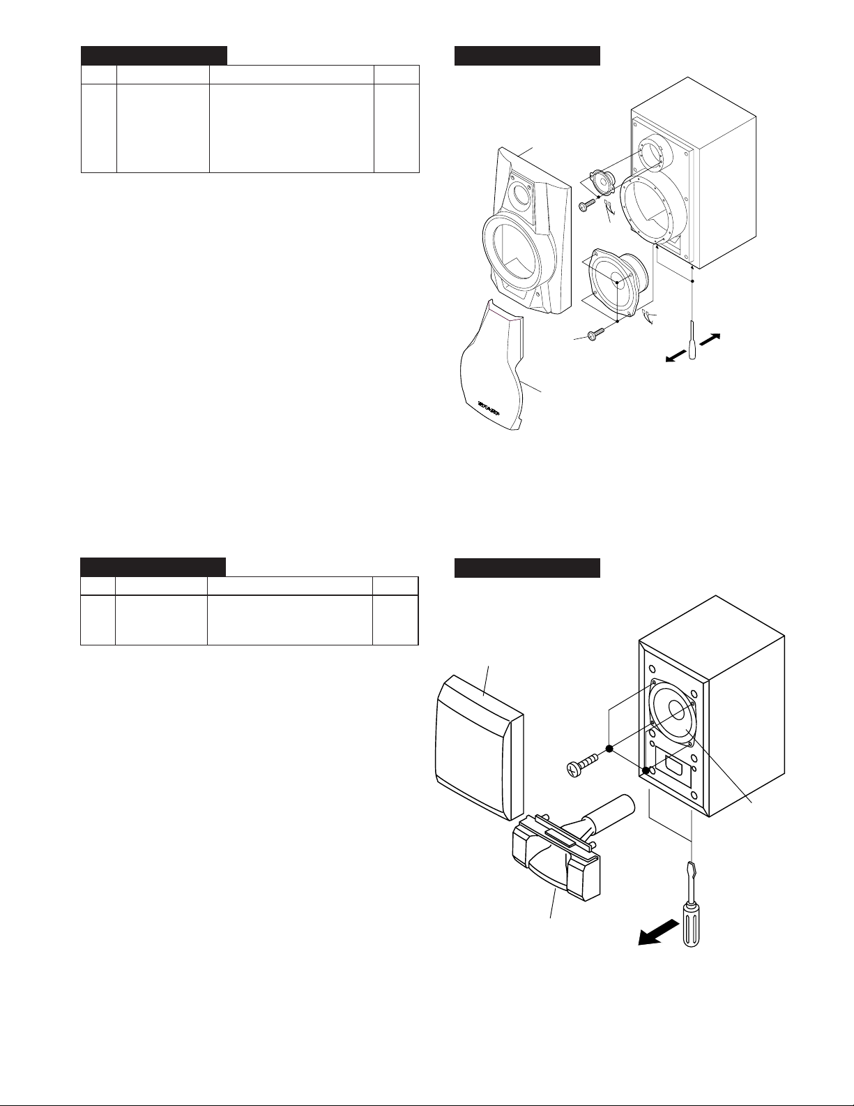
CD-PC672
CP-C672
STEP REMOVAL
1 Front Speaker 1. Net.......................... (A1) x1 11-1
2. Front Panel ............ (A2) x1
3. Screw ..................... (A3) x4
4. Tip .......................... (A4) x2
5. Screw ..................... (A5) x2
6. Tip .......................... (A6) x2
PROCEDURE
FIGURE
CP-C672
Front Panel
(A2)x1
Net
(A1)x1
(A3)x4
(A5)x2
(A6)x2
Figure 11-1
(A4)x2
Screw Driver
CP-SW672
STEP REMOVAL
1 Front Speaker 1. Net.......................... (A1) x1 11-2
2. Duct Panel ............. (A2) x1
3. Screw ..................... (A3) x4
PROCEDURE
FIGURE
Note:
The rear speakers and center speaker can be easily
disassembled.
Therefore the disassembling method is not described.
For details refer to the disassembling drawing in the Parts
Guide.
CP-SW672
Net
( A1 ) x1
( A3 ) x4
ø4 x16mm
( A2 ) x1
Woofer
Screwdriver
Figure 11-2
– 11 –
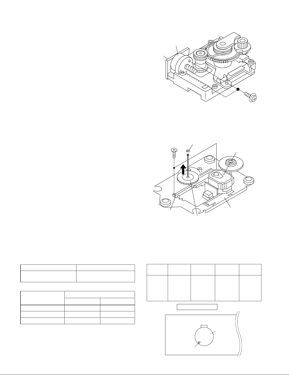
CD-PC672
( B1 ) x2
ø2.6 x6mm
Shaft
( B2 ) x1
Stop Washer
( B3 ) x1
Gear
( B4 ) x1
CD Mechanism
Pickup
REMOVING AND REINSTALLING THE MAIN PARTS
CD MECHANISM SECTION
Perform steps 1, 2, 3 and 10-14 of the disassembly method to
remove the CD mechanism.
Loading / Up
/ Down Motor
How to remove the loading motor
(See Fig. 12-1)
1. Remove the screws (A1) x 2 pcs., to remove the loading
motor.
How to remove the pickup (See Fig. 12-2)
1. Remove the screws (B1) x 2 pcs., to remove the shaft (B2).
2. Remove the stop washer (B3) x 1 pc., to remove the gear
(B4).
3. Remove the pickup.
Note
After removing the connector for the optical pickup from the
connector, wrap the conductive aluminium foil around the
front end of connector to protect the optical pickup from
electrostatic damage.
Motor
PWB
( A1 ) x2
ø2.6 x5mm
Figure 12-1
MECHANISM SECTION
• Driving Force Check
Play: TW-2412 Tape 1: Over 80 g
• Torque Check
Play: TW-2111 30 to 60 g. cm 30 to 60 g.cm
Fast forward: TW-2231 — 60 to 120 g.cm
Rewind: TW-2231 — 60 to 120 g.cm
Torque Meter
Torque Meter
Specified Value
Tape 2: Over 80 g
Specified Value
Tape 1
ADJUSTMENT
Tape 2
– 12 –
Figure 12-2
• Tape Speed
Test Tape
Normal MTT-111 Varioble 3,000 ± Speaker
speed resistor in 30 Hz terminal
TAPE MECHANISM
Varioble resistor in motor
Adjusting
Point
motor. (Load
(MM1) resistance:
Figure 12-2
Specified
Value
MM 1
Motor
Instrument
Connection
8 ohms)
CD-PC672
Pin 13 of IC303
Pin 21 of IC303
D
G
S
10 kΩ
TO FREQUENCY
COUNTER
FET : 2SK19 or 2SK54
TUNER SECTION
fL: Low-range frequency
fH: High-renge frequency
• AM IF/RF
Signal generator: 400 Hz, 30%, AM modulated
Test Stage Frequency
Frequency
Display
IF 450 kHz 1,720 kHz T382 *1
Band — 530 kHz (fL): T333 *2
Coverage 1.1 ± 0.1 V
Tracking 990 kHz 990 kHz (fH): T331 *1
*1. Input: Antenna, Output: TP302
*2. Input: Antenna, Output: TP301
• FM RF
Signal generator: 1 kHz, 75 kHz dev., FM modulated
Test Stage
Frequency
Band — 87.50 MHz T301(fL): *1
Coverage 3.4 V ± 50 mV
RF 98.00 MHz 98.00 MHz L312 *2
(10-30 dB)
Frequency
Display
*1. Input: Antenna, Output: TP301
*2. Input: Antenna, Output: Speaker terminal
Setting/
Adjusting
Parts
Serring/
Adjusting
Point
Instrument
Connection
Instrument
Connection
• VCO Frequency
Frequency
Frequency
Display
98.00 MHz 98.00 MHz VR381* Pin 13, Pin 21
(60 dB) and ground
Adjusting
Parts
Instrument
Connection
of IC303
* Adjust for 76 kHz ± 200 Hz.
Notes:
After preparing the test circuit shown in Fig 13-2, connect the
Pin 13 , Pin 21 and ground of the IC303 with test circuit, and
measure the Value.
At this time, apply a standard unmodulated signal input and
adjust the VCO.
MAIN PWB
IC301
T302
FM IF
T333
FM DET
1
L312
FM RF
T331
CNP301
AM LOOP
ANTENNA
AM TRACKING
fH
AM BAND
COVERAGE fL
FM BAND
COVERAGE fL
TP301
13
IC386
IC302
AM IF
IC303
VR381
VCO
20
1
22
T301
T382
21
TP302
1
T381
• Detection
Signal generator: 10.7 MHz, FM sweep generator
Test
Frequency
Stage
Detection 10.7 MHz 98.00 MHz T381 Input: Pin 1 of
IF 10.7 MHz 98.00 MHz T302(Turn Input: Pin 1 of
Frequency
Display
Adjusting
Parts
Instrument
Connection
IC303
Output: TP302
the core of IC301
transformer Output: TP302
T381 fully
counterclookwise.)
CD ERROR CODE DESCRIPTION
When a malfunction occurs during CD operation, an error
code will be displayed to identify the function in CD operation
which failed.
Error State Code
0001 Cannot detect pickup in SW
0101 Tray close operation error
0105 Tray close operation error
0201 Tray open operation error
0203 Tray open operation error
0304 Disc skip operation error
0305 Disc skip operation error
0307 Disc skip operation error
Figure 13-1 ADJUSTMENT POINTS
Figure 13-2
– 13 –
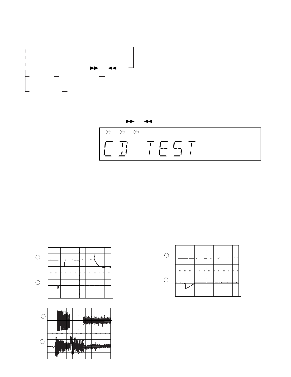
CD-PC672
1 2 3
TEST MODE
• Setting the test mode
Any one of test mode can be set by pressing several keys as follows.
<REC. PAUSE> + <DISC. SKIP> + <POWER> TEST: CD operation test
• TEST mode
Function — CD test mode
Setting of TEST mode
Indication of CD TST mode (Fig. 14-1)
OPEN/CLOSE operation is manual operation.
The pickup can be moved by using the (
<MEMORY>
LASER ON
<MEMORY>
Tracking on the spot.
SERVO OFF PLAY
) or ( ) key.
<MEMORY>
Tracking on the spot.
SERVO ON PLAY
IL is not performed.
<STOP>
STOP
<PLAY> key input
TOC. IL is performed, and the ordinary PLAY is performed.
If the following key is pressed during PLAY, it is possible
to specify directly any Track No.
<Disc Number 1> key: Track 4
<Disc Number 2> key: Track 9
Press <STOP> key.
Stop
<Disc Number 3> key: Track 15
Note:
Only in STOP state it is possible to slide the pickup with the ( ) or ( ) key.
VOL. --- Last memory
BAL. --- CENTER
R.GEQ. --- FLAT
X-BAS --- OFF
Canceling method - POWER OFF
Figure 14-1
CD SECTION
Since this CD system incorporates the following automatic adjustment function, when the pickup is replaced, it is not necessary
to readjust it.
Since this CD unit does not need adjustment, the combination of PWB and laser pickup unit is not restricted.
• Automatic adjustment item
1. Focus offset (Fig. 14-2)
2. Tracking offset (Fig. 14-3)
3. E/F balance (tracking error balance) (Fig. 14-4)
4. RF level AGC function (HF level: constant)
5. RF level automatic follow-up of the tracking gain
This automatic adjustment is performed each time a disc is changed. Therefore,
each disc is played back using the optimal settings.
0.1s
0.50 V
IC1 20 FE
FOCUS
OFF-SET
ADJUST
0.1s
0.50 V
IC1 7 TE
TRACKING
OFF-SET
ADJUST
1
2
Figure 14-2
200 ms
1V/diV
IC 1 15
200 ms
1V/diV
IC 1 7
TO
TE
TRACKING/
ERROR
BARANCE
1
ADJUST
2
Figure 14-4
– 14 –
10ms
0.50 V
IC1 20 FE
10ms
0.50 V
IC1 7 TE
Figure 14-3
Enlarged
View
TRACKING
OFF-SET
ADJUST
1
2
CD-PC672
EXPLANATION OF DOLBY SURROUND PRO LOGIC AND EVALUATION METHOD
Outline
• Namely, two speakers are connected in parallel to one
amplifier.
• In the Pro Logic BYPASS mode the amplifier for C-ch (center
channel) and the amplifier for S-ch (surround channel) are in
MUTE state. The SP output is cut.
• State of element output and terminal output in specific mode
State of set Dolby Pro Logic Dolby Pro Logic On mode
Output point Bypass mode Normal mode Phantom mode
IC501 12 pin L-out Output enabled state Output enabled state Output enabled state
11 pin R-out Output enabled state Output enabled state Output enabled state
IC501 9pin C-out No output Output enabled state No output
IC501 10pin S-out No output Output enabled state Output enabled state
SP OUT L-ch Output enabled state Output enabled state Output enabled state
(SO901) R-ch Output enabled state Output enabled state Output enabled state
SP OUT C-ch No output in MUTE (Q404) state Output enabled state No output in MUTE (Q404) state
(SO901)
SP OUT S-ch No output in MUTE (Q403) state Output enabled state Output enabled state
(SO901)
Test tone output
• Pro Logic ON Normal mode
Press the remote control TEST TONE button.
→Output of only L-ch →Output of only C-ch
↑ ↓
Output of only S-ch ← Output of only R-ch
The test tone (noise) is repeatedly output for output period
(2 sec).
In this case the following indication appears repeatedly.
→TEST →L-ch →C-ch
↑ ↓
S-ch ← R-ch
• Pro Logic ON Phantom mode
Press the remote control TEST TONE button.
→Output of only L-ch →Output of only R-ch
↑ ↓
← Output of only S-ch
The test tone (noise) is repeatedly output for output period
(2 sec).
In this case the following indication appears repeatedly.
→TEST → L-ch → R-ch
↑ ↓
← S-ch←
Relation between VIDEO IN input and output in Pro Logic
ON state
(1) L-ch/R-ch same phase input into VIDEO IN input jack in
VIDEO Function mode
Output point Normal mode
SP out L-ch Almost no output (only omitting component)
(SO901) R-ch Almost no output (only omitting component)
(SO901) SP out C-ch
(SO901) SP out S-ch
Input signal is output.
Almost no output (only omitting component)
• In the normal mode of Pro Logic ON mode the amplifiers for
C-ch and S-ch are in operative state, so that the SP output
appears.
• In the Phantom mode of Pro Logic ON mode the amplifier for
C-ch is in MUTE state, so that the SP output is cut. The
amplifier for S-ch (surround) is in operative state, so that the
SP output appears
Output point Phantom mode
SP out L-ch Input signal is output.
(SO901) R-ch Input signal is output.
(SO901) SP out C-ch SP cut, no output
(SO901) SP out S-ch
Almost no output (only omitting component)
(2) L-ch/R-ch reverse phase input into VIDEO IN input jack in
VIDEO Function mode
(Reverse phase: Phase difference between L and R is 180°)
Output point Normal mode
SP out L-ch
(SO901) R-ch
(SO901) SP out C-ch
(SO901) SP out S-ch Input signal is output.
Output point Phantom mode
SP out L-ch
(SO901) R-ch
(SO901) SP out C-ch SP cut, no output
(SO901) SP out S-ch Input signal is output.
Almost no output (only omitting component)
Almost no output (only omitting component)
Almost no output (only omitting component)
Almost no output (only omitting component)
Almost no output (only omitting component)
• Accordingly, if you want to output signal waveform to C-ch SP
out, give the same phase input into L-ch/R-ch INPUT in the
Pro Logic Normal mode.
If one of channels receives input, C-ch does not output. Only
L-ch or R-ch outputs.
• If you want to output signal waveform to S-ch SP out, you can
use either Normal mode or Phantom mode. However, 180°
reverse phase input must be given to L-ch/R-ch INPUT.
– 15 –
CD-PC672
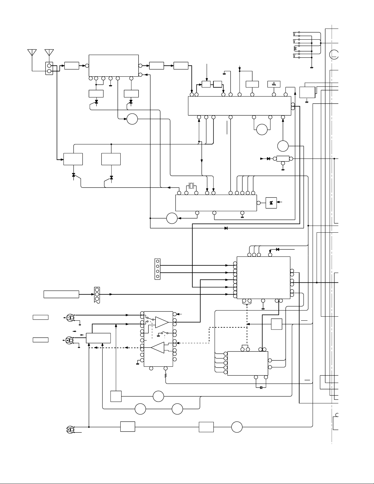
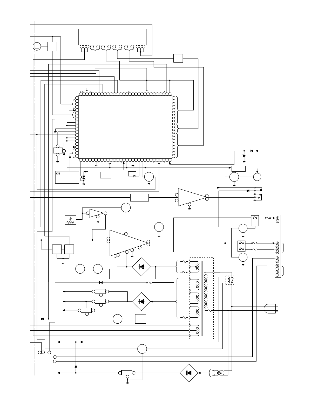
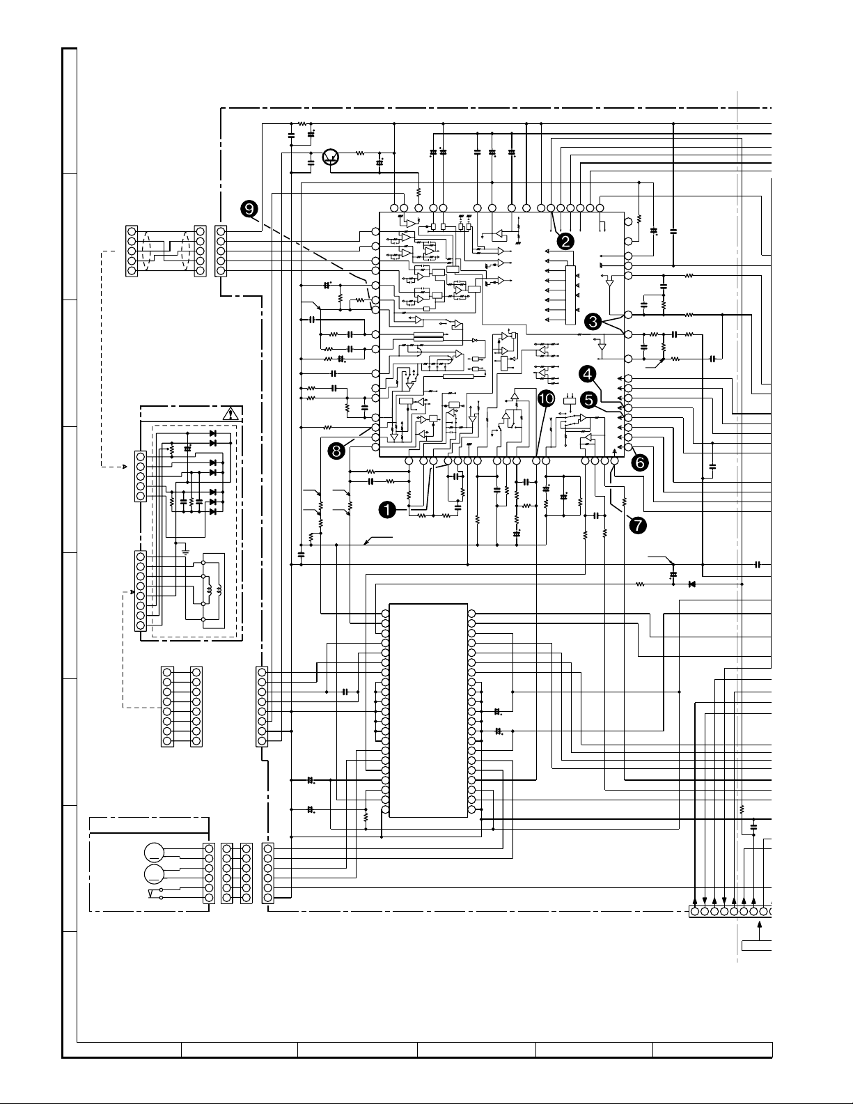
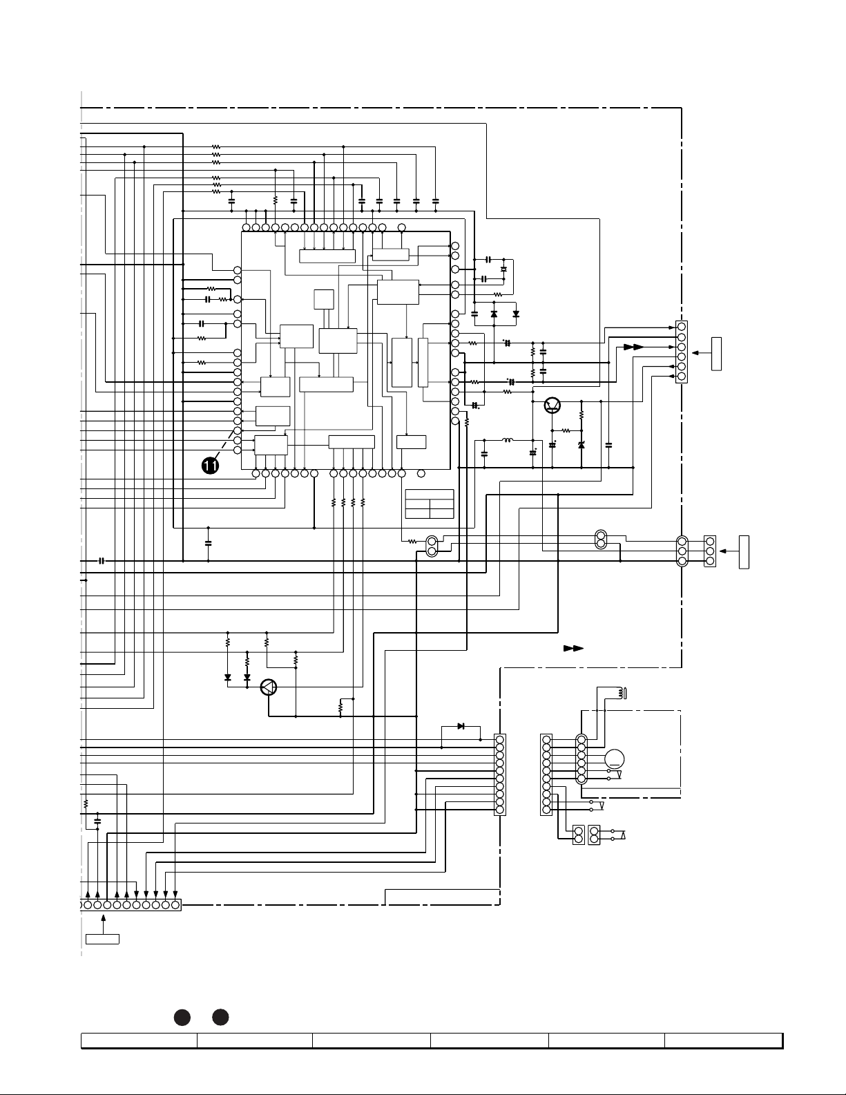
NOTES ON SCHEMATIC DIAGRAM
• Resistor:
To differentiate the units of resistors, such symbol as K and
M are used: the symbol K means 1000 ohm and the symbol
M means 1000 kohm and the resistor without any symbol is
ohm-type resistor. Besides, the one with “Fusible” is a fuse
type.
• Capacitor:
To indicate the unit of capacitor, a symbol P is used: this
symbol P means micro-micro-farad and the unit of the
capacitor without such a symbol is microfarad. As to
electrolytic capacitor, the expression “capacitance/withstand
voltage” is used.
(CH), (TH), (RH), (UJ): Temperature compensation
(ML): Mylar type
(P.P.): Polypropylene type
• Schematic diagram and Wiring Side of P.W.Board for this
model are subject to change for improvement without prior
notice.
• The indicated voltage in each section is the one measured
by Digital Multimeter between such a section and the chassis with no signal given.
1. In the tuner section,
( ) indicates AM
< > indicates FM stereo
2. In the main section, a tape is being played back.
3. In the deck section, a tape is being played back.
( ) indicates the record state.
4. In the power section, a tape is being played back.
5. In the CD section, the CD is stopped.
• Parts marked with “ ” ( ) are important for
maintaining the safety of the set. Be sure to replace these
parts with specified ones for maintaining the safety and
performance of the set.
REF. NO DESCRIPTION POSITION POSITION
SW1 OPEN/CLOSE ON—OFF
SW2 MECHA UP ON—OFF
SW3 DISC NUMBER ON—OFF
SW4 PICKUP IN ON—OFF
SW701 POWER ON—OFF
SW703 CLOCK ON—OFF
SW704 TIMER/SLEEP ON—OFF
SW705 DISC 1 ON—OFF
SW706 DISC 2 ON—OFF
SW707 DISC 3 ON—OFF
SW708 DISC SKIP ON—OFF
SW709 OPEN/CLOSE ON—OFF
SW710 REW ON—OFF
SW711 REC PAUSE ON—OFF
SW712 MEMORY/SET ON—OFF
SW713 STOP ON—OFF
SW714 TUNER/BAND ON—OFF
FRONT
VIEW
FRONT
VIEW
REF. NO DESCRIPTION
SW715 VIDEO ON—OFF
SW716 TAPE ON—OFF
SW717 CD ON—OFF
SW722 FF ON—OFF
SW723 TUNING UP ON—OFF
SW724 TUNING DOWN ON—OFF
SW725 PLAY ON—OFF
SW728 X-BASS/DEMO ON—OFF
SW729 EQUALIZER ON—OFF
SW730 DIMMER ON—OFF
SW731 PHANTON ON—OFF
SW732 NORMAL ON—OFF
SW733 BYPASS ON—OFF
SWM 3 FOOL PROOF ON—OFF
SWM 4 F.A.S. ON—OFF
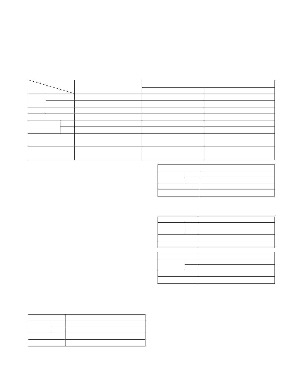
E C B
(S)(G)(D)
(1) (2) (3)
KRA102 M
KRA109 M
KRC102 M
KRC104 M
KRC107 M
KTA1266 GR
KTA1271 Y
KTA1273 Y
KTC3203 Y
KTC3194 Y
KTC3199 GR
2SC2389 SE
KTA1274 Y
Figure 16 TYPES OF TRANSISTOR AND LED
B C E
(D)(G)(S)
(3) (2) (1)
2SA1318
– 16 –
1 2 3
SVC211C
SVC348S
FRONT
VIEW
L1154GT4
SLI342YCB
SLI342DCB
SLI342UCB
SLI342YCJ
SLI3256YC
SLI342UCJ1
TO MAIN SECTION
(TO IC601)
SW2
MECHA UP
10
9
SW3
8
SW1
DISC No.
7
6
M3
LOADING
OPEN/CLOSE
M
5
2
3
4
SOLM1
1
CD-PC672
TO MAIN
SECTION
CNS10
+7.3V (B1)
CNP99
+5V
+5V
+B1
Q52
Q1
3
XL1
+5V
2
1
BI1A
BI1B
43
41
36
23
44
45
64
62
1
2
1
2
1
31 38 39 40
XVDD
RVDD
LVDD
VDD
VVDD
6
SERVO/SIGNAL
XOUT
XIN
2
4 8
22
VCC1
SERVO AMP.
LD0
2
5
4
6
3
37
LVSS
RVSS
LCHO
RCHO
IC2
LC78622NE
CONTROL
EFMO
EFMIN
10 12 20
11
9
~
32 40 4344
JP–
IC1
LA9241M
FIN2
2
1
CNP11
Q51
27
CLV+
~
SLC
CV+
FIN1EF
3
4
24 25
CONT2
CONT1
RES. CQCK. COIN
JP–
CE
SL1
DAT
CL
DRF
SL+
SL–
SLD
NC
SPO
FD
TO
46
39
38
33
26
58
~
53
64
~
SQOUT. RWC. WRQ
62
51
53
52
51
54
31
30
29
23
27
16
15
CL, DAT, SELIAL CONTROL/CE
GND (D)
MECHA UP
GND (D)
DISK NO.
10
7
9
8
SL+. SL–. DRF
25
20
7
2
1
23
6
OPEN/CLOSE
GND (D)M–M+
5
2
3
6
4
+B1
+B5
18244020
IC3
M63001FP
FOCUS/
TRACKING/
SPIN/SLED
DRIVER
15
7
45
GND (M)
1
CNP10
3839284142 37 36
16 26
PU-IN SW
35
29
22
21
14
~~
8
27
Q81
REGULATOR
+4.3V
FOCUS COIL
TRACKING COIL
PICKUP UNIT
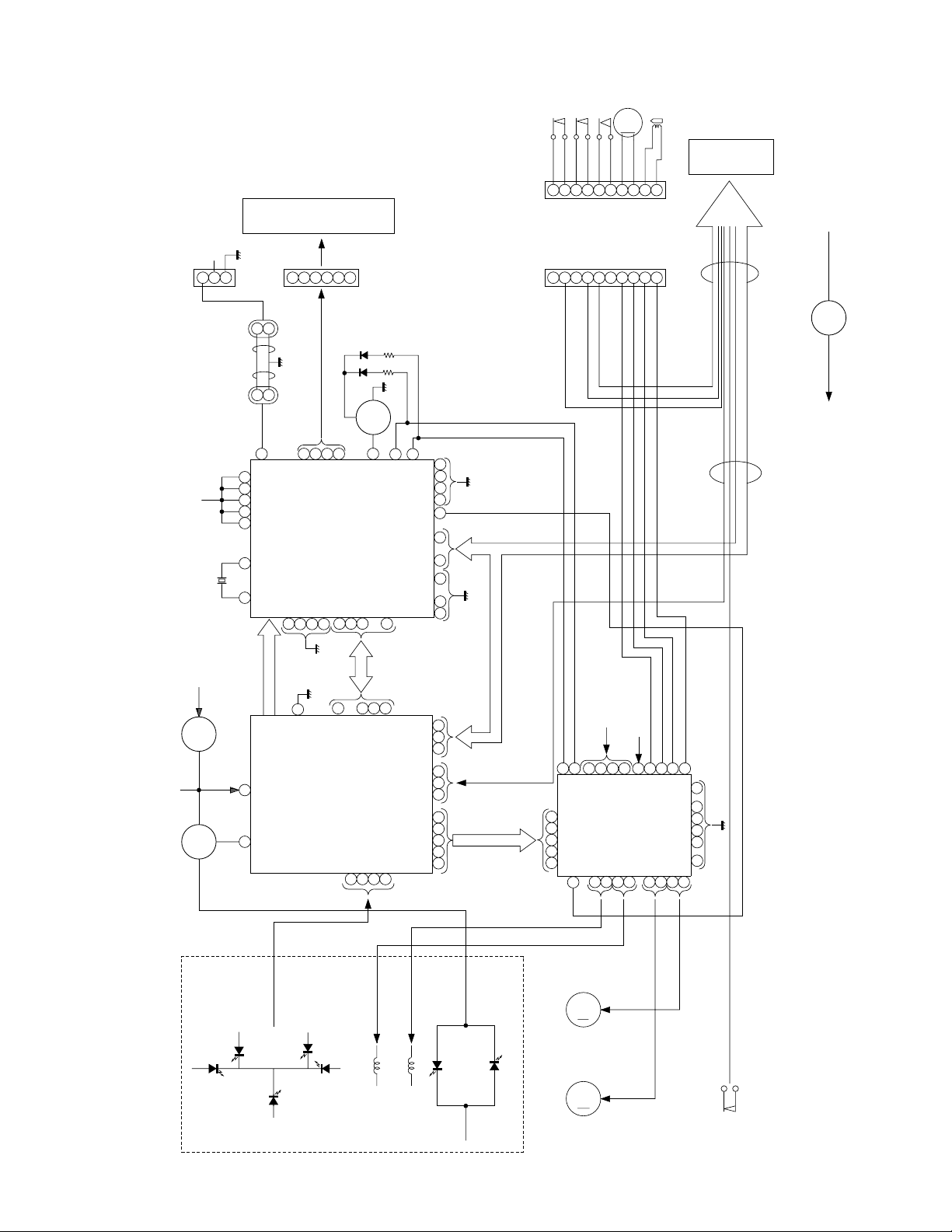
Figure 17 BLOCK DIAGRAM (1/3)
– 17 –
M1
SPINDLE
MOTOR
M
M2
SLED
MOTOR
M
PICKUP IN
SW4
CD-PC672
9
4
O
3
O
AM LOOP
FM
ANTENNA
ANTENNA
1
L301
FM B.P.F
AM TRACKING
T331 T333
FM FRONT END
2 3 4
L312
IC301
TA7358AP
5
7
FM
OSC
FM RF
OSC BUFF
AM OSC
8
T301
Q301
6
9
FM OSC
FM IF
T301
VT
FM +B
CF301
FMOSC
Q351
SWITCHING
FM IF IN
4.5MHz
20
1
FM
+B4
AM IF
T382
1 3
AM MIX
LA1805
FM/AM IF MPX.
24
23
AM+B
AM OSC IN
X352
22
15
OSC
LC72131
PLL (TUNER)
7
CF351
IC303
22
AM RF IN
FM IN
AM IN
16
IC302
10
+B4
T381
FM DET
21
5
6
GND AM IF
7
STEREO
11
20
FM DET
FM+B MO/ST
DET OUT
17
+B7
CE
3 4
6
5
21
MPX VCO ADJ
MPX IN
Q382
FM/AM
SWITCHING
DODICL
VOLTAGE
REGURATER
17
SWM3
FOOL PROOF
SWM4
F.A.S
SOLM1
SOLENOID
SWM5
CAM
VR381
MONO/ST
15
13
VCO
L
9
10
R
FM/AM
16
11
Q381
IC704
3
1
2
+B4
VOLUME
JOB
VR702
M
MM
TAPE M
FROM CD SECTION
CNP11
TAPE 1
PB HEAD
TAPE 2
REC PB HEAD
L-CH
R-CH
L-CH
R-CH
ERASE
HEAD
REC
P.B
AC BIAS
CNS11
1
2
3
SWITCHING
Q103~Q106
VIDEO IN
L
R
L
R
PLAYBACK AND RECORD
R(T1)
R(T2)
POP REDUCE
L REC
R REC
SWITCHING SWITCHING
Q107
Q108
BIAS
OCS
Q128
L104
AN7345K
/PLAYBACK AMP.
L(T1)
1
24
L(T2)
2
23
L NF
3
4
R NF
T1/T2
6
REC
9
16
14
REF
12
NOR/
HIGH
15 19
Q109
SWITCHING
JK401
IC101
Q111
P.B.
H/N
T1/T2
13
4
21
5
20
7
18
8
17
10
Q110
L
R
L R REC
L NF
R NF
ALC
+B4
PB
SWITCHING
Q124
VIDEO2
VIDEO1
TAPE
TUNER
CD
23 24 25
L
R
L
R
L
R
L
R
L
R
34
IC501
38
LV1035M
35
DOLBY PRO LOGIC
37
DECORD
36
CLDICE
51
61
52
60
59
58
BAIS
Q126
LC75396N
53
AUDIO PROCESSOR
54
55
57
63
49
L
44
R
45
33 32
IC401
9
33
48
X501
56
Q121
Q122
MUTING
22
9
+B4
20
28
R
17
31
L
30
18
33
48
REC
Z
T1/T2
1
IC
BAIS
LA
P
Figure 18 BLOCK DIAGRAM (2/3)
– 18 –
M
MM1
APE MOTOR
Q702
Q703
~~~
1 2 3
4
DISPLAY
15 2516
FL701
26
CD-PC672
~
28
36
37 3839
29
Q705
Q706
Q707
ZD801
+B7
+B7
1
RX701
3
2
+B7
KEY
SW703~SW717
SW722~SW725
SW728~SW733
VR701
Q401
Q402
+B4
+B5
+B2
50
49
48
47
46
45
44
43
42
41
40
39
38
37
36
35
34
33
32
31
Sub Woofer
Volume
Q403
Q404
REGULATOR
+12V(ANALOG)
+12V(MOTOR)
+5.6V
535251
VDD
AVDD
282930
PHM1
VOLTAGE
IC806
2
SYSTEM CONTROL
MICROCOMPUTER
+B5
IC650
IC651
KIA4558P
OPE AMP.
IC471
37
4
IC901
16
STK40704
12
POWER AMP.
Q903Q405
D802
VOLTAGE
REGULATOR
13
IC804
2
VOLTAGE
REGULATOR
13
IC805
2
13
VOLTAGE
REGULATOR
IC701
IX0310AW
VDD
+B7
Q904
18
+B
3
–B
2
1
Q801
XL701
4.19MHz
Q601,Q602
Q603, Q604
15
D801
D803~D806
D807
~D809
7170696867666564636261 80797877
737260595857565554
101112131415161718192021222324252627
8
9
7
Q704
FRONT
L-OUT
9
8
R-OUT
20
3A/250V
6
F804
767574
4 3 2 1
5
Q908
81
82
83
84
85
86
87
88
89
90
91
92
93
94
95
96
97
98
99
100
VDD
IC601
3
NJM4560D
OPE AMP.
5
F802
5A/125V
F803
5A/125V
F805
2A/250V
4
PT801
POWER
TRONSFORMER
UNSWITCH
+B7
MEMORY
BACK UP
TO CD
SECTION
Q905
+B5
1
7
+B1
M901
M
FAN MOTOR
JK970
HEADPHONES
F903
RL901
4A/125V
Sub Woofer
Q907
RL902
F902 4A/125V
Front
Speaker
Center
Speaker
Rear
Speaker
SO901
Speaker Terminal
T.F
Q906
RL801
F901 4A/125V
AC POWER
SUPPLY CORD
AC 120V, 60Hz
9
13
7
IC951
LA4551
POWER AMP.
+B6
1
6
+B7
+5V
UNSWITCH
Q802
13
IC803
2
D811~D814
Figure 19 BLOCK DIAGRAM (3/3)
– 19 –
PT802
POWER
TRONSFORMER
CD-PC672
2
SLD+
D
A
CNS1B
K
5
E
B
4
A
3
B
2
F
1
C
K
E
A
D
B
F
E
F
CD MOTOR PWB-D
M1
SPINDLE
MOTOR
G
M2
SLED
MOTOR
SW4
PICKUP IN
CNS1A
1
2
3
4
5
PICKUP UNIT
1
2
3
4
5
6
7
8
+
–
+
–
1M
2200P
TR–
TR+
FO+
FO–
GND
PD
VR
LD
SLIDE
PU-IN
SPIN
1/16
1M
2200P
TR+
FO+
FO–
TR–
ACTUATOR
CNS2ACNS2B
1
2
3
4
5
6
7
8
6
5
4
3
2
1
5
4
3
2
1
1
2
3
4
5
6
7
8
M
M
1
2
3
4
5
CNP1
6
5
4
3
2
1
CNS3B
CNP3A
K
A
B
E
F
TR–
TR+
FO+
FO–
GND
PD
VR
LD
6
5
4
3
2
1
1
2
3
4
5
6
7
8
CNP2
CNS3A
R2
1K
C15
0.01
C2
0.01
C54
R13
PD
TR–
TR+
FO+
FO–
LD
CD_GND
100/16
6
5
4
3
CD_PUIN
2
1
CNP3
C1
47/16
R1
22
1/50
Q1
2SA1318
IC1
LA9241M
SERVO AMP.
C4
R11
R12
100
R14
27K
R16
3.3K
C12
0.1
0.047
R22
100K
C9
820
R9
R10
2.2K
C6 0.033
0.068
R15
12K
1K
R20
R21
1.5K
0.022
R8
15K
C5
0.033
0.1/50
C8
C76
C7
C10
180P
R19
R56
0.1/50
TE
0.001
6.8K
1K
C36
100/16
C55
SP+
SP–
SL_+
SL_–
C3
R17
33K
C11
0.1
1K
6.8K
1
2
3
4
5
6
7
8
9
10
11
12
13
14
TO
15
FD
16
VREF
VCC1
FIN2
REF
FIN1
REF
E
F
TB
TE–
TE
TESI
SCI
TH
NC
TD–
TD
JP
R18
15K
1
2
3
4
5
6
7
8
9
10
11
12
13
14
15
16
17
18
19
20
21
64
C34
0.33/50
63 62
LDS
–
+
–
+
–
+
REF
REF
REF
REF
–
+
GEN
REF
+
–
FD–
17
TO
FD
FO (GAIN)
FO+
FO–
TR+
TR–
GND
SL–
SL+
SLD
VCC1
STANDBY
Vref
MUTE
C32
0.01
C33
0.47/50
560
R46
60
61
BHI
LDO
RF
–
+
–
+
–
+
+
–
REF
+
REF
–
TO
REF
+
–
GEN
REF
+
–
FA
FA–
18
19
R23 10K
R24
47K
IC3
M63001FP
59
PHI
FE1
REF
VCR
VCR
–
VCR
+
VCR
+
–
+
–
TGL1
THDL
JP
FSC
FOSTA
REF
GEN
+
–
+
–
REF
FE
AGND
SP
FE–
21
23
22
20
C13
330P
R26
82K
C14
0.01
R25
1.5K
42
LD_M+
41
LD_M–
40
VCC4
M–
39
M+
38
SOL–
37
36
SOL+
35
34
33
32
GND
31
30
29
28
VCC3
27
SP+
SP–
26
25
SPO
(SPN)
24
VCC2
23
SOLD
22
SOL–
FOCUS/TRACKING/SPIN/SLIDE DRIVER
REF
R27
39K
LF2
GL
THD
58
VR
–
+
VCC
REF
FE1
REF
SPI
24
C16
0.0047
1.2K
C82
100/16
C77
100/16
C31
220/6.3
+
–
+
–
+
–
+
–
+
–
S.Q.R
REF
+
–
SPG
25
R28
R31
0.47/50
57
REF1
DEF
HFL
DRF
FSTA
+
26
10K
C18
C30
–
SP–
0.001
0.1/50
56
EFBAL
FOSTA
TOSTA
2FREQ
LASER
8/12CM
REF
REF
JP
C17
R29
R30
6.8K
VCC2
FSTA
SLOF
SPO
27
56K
55
FSS
+
–
+
–
REF
SLEO
28
1.2K
54 53
DRF
SLOF
SLOF
C20
47/16
R33
52
CE
DAT
CV–
CV+
JP–
JP+
JPCLO
OR
REF
C19
1/50
R32
10K
R34
3.3K
51
CL
CE
CL
LATOH
SLOF
SLD
REF
29
+
–
50
FSC
REF
RF
+
–
CLK
30
49
DEF
+
SL–
C21
NC
TBC
DGND
SLI
+
–
SLC
RFS–
–
RFSM
CV+
CV–
SLOF
HFL
TES
TOFF
TGL
JP+
JP–
SL+
31
32
0.0033
R35
220K
R45
4.7K
48
C29
4.7/50
C28
0.001
R40
5.6K
HF
TP1
220K
GND
C24
2.2P
C26
0.033
R41
47K
C25
27P
R43
56K
R38
470
0.1
C35
1/50
R44
33K
R42
47K
R39
1K
D1
1SS133
C23
0.0027
C22
220P
C57
0.001
47
46
45
44
C27
43
42
41
40
39
38
37
36
35
34
33
R36
R37
82K
+B
R47
10K
C37
0.02
CQ CK(DSP)
CO IN(DSP)
SQ OUT(DSP)
D_GND
RES(DSP)
WRQ(DSP)
CNP12
RWC(DSP)
1 2 3
DRF(ASP)
4
6
5
8
7
CNS12
FROM DISPLA
P29 12-
H
• NOTES ON SCHEMATIC DIAGRAM can be found on page 16.
1
23456
Figure 20 SCHEMATIC DIAGRAM (1/12)
– 20 –
C57
0.001
R51
3.3M
C39
0.047
R57 1K
R58 1K
R59 1K
R61 1K
R62 1K
R63 1K
R50
680
C40
0.047
R52
27K
R53
1.2K
C56
0.022
14
10
11
12
13
15
16
C38
0.01
1
2
3
4
5
6
7
8
9
64
TEST1
DEF1
TA1
PDO
VVSS
ISET
VVDD
FR
VSS
EFMO
EFMIN
TEST2
CLV+
CLV–
V/P
HLF
TES
1K
R60
63
62
61
/CS
TEST5
LC78622N
SLICE
LEVEL
CONTROL
CLV
DIGITAL
SERVO
SERVO
COMMAND
TGL
TOFF
18
17
19
C46
60
4M
16M
CONTROL
JP+
JP–
20
100P
59
NC
IC2
VCO
CLOCK
OSC
21
(CH)
58
55
56
57
/RES
COIN
/CQCK
SQOUT
TEST11
MICRO-COM
INTERFACE
NC
2KX8
RAM
ERROR
COERECT
FLAG
CONTROL
SYNC-DETECT
EFM DEMODULATE
SERVO/
SIGNAL
CONTROL
NC
NC
CONT1
PCK
FSEQ
VDD
22
23
24
R88 1.2K
54
52
53
FSX
RWC
WRQ
NC
EXTERNAL
OUTPUT
CONT2
CONT3
27
26
25
R90 220
R89 1.2K
C44
100P(CH)
51
50
SFSY
SBCK
SUB-CODE
GENERATOR
CONT4
EMPH
CONT5
29
28
NC
R91 1K
C45
100P(CH)
49
NC
X-TAL
4FS
C2F
31
30
NC
NC
R54
330
C47
C48
100P
100P(CH)
NC
PW
NC
XVDD
MUTER
RVDD
RCHO
FILTER
DIGITAL
1BIT DAC
MUTEL
TEST4
DIGITAL
OUT
NC
DOUT
TEST3
32
PIN27
TRY SPEED
HIGH
LOW
BI1-B
2
1
EFLG
SBSY
XVSS
XOUT
RVSS
LVSS
LCHO
LVDD
C49
NC
XIN
NC
NC
100P(CH)
48
47
46
45
44
43
42
41
40
R72
39
2.7K
R71
38
2.7K
37
36
35
34
33
R65
1K
C41
12P
C42
15P
R93
220
C83
0.022
C71
10/50
C43
330/6.3
D81
L61
0.82µH
C50
0.022
XL1
16.934MHz
D82
1SS133
C72
10/50
R74
100K
R73
100K
R55
100
C51
100/16
1SS133
+5V
CD_RCH
C74
220P
C73
220P
KTC3203 Y
R64
22
C52
100/16
A_GND
CD_LCH
Q52
R66
220
ZD61
MTZJ5.6B
BI1-A
2
1
CD-PC672
R-CH
1
A_GND
2
L-CH
3
D-GND
4
+7V
+12V
+B
C75
0.001
+B
BI99
5
6
CNP11
CNS11
P22 6-A
FROM MAIN PWB
CNP99
3 3
2 2
1 1
CNS99
P31 12-B
R47
10K
C37
0.022
D_GND
RES(DSP)
DRF(ASP)
SLD+
6
8
9
7
CNS12
DISPLAY PWB
P29 12-D
SLD–
PUIN SW
11
10
OP/CLOS
DISC NO.
14
12 13
PCCL
UP/DOWN
15
R82
390
D92
R83
1SS133
D93
1SS133
390
KRC102 M
Q51
R80
820
R81
820
R84
2.2K
D91
1SS133
M+
M–
CD_D_NO
CNP10
CD SERVO PWB-B
+B
SOL+
1
SOL–
2
M+
3
M–
4
GND(D)
5
OPEN CLOSE
6
DISC NO.
7
GND(D)
8
MECHA UP
9
10
GND(D)
1
2
3
4
5
6
7
8
9
10
CNS10
CD SIGNAL
SOLM2
SOLENOID
TURNTABLE
BIM5
1
2
3
4
5
6
CD SENSOR PWB-E
1
2
CNS5
UP/DOWN
LOADING MOTOR
–
M
+
OPEN/CLOSE
SW2
MECHA UP
1
DISC NUMBER
2
TO DIGITAL OUT PWB
M3
SW1
SW3
• The numbers 1 to 12 are waveform numbers shown in page 41.
7
8 9 10 11 12
Figure 21 SCHEMATIC DIAGRAM (2/12)
– 21 –
CD-PC672
M
0
0
C438 22/25
M
3
A
TO TUNER SECTION
P27 12-F
123456789
DI
CE
DO
A_12V
TUN_L
TUN_R
A_GND
TUN_SM
TO DECK SECTION
P25 12-B
10 11 12 13 14 15 16 17 18 19 20 21
CL
D_GND
BIAS
T1/T2
A_12V
D_GND
REC_MUTE
M_GND
REC_R
A_GND
+B
REC_L
TAPE_L
TAPE_R
TO CD SERVO PWB
P21 12-C
CNP11
123456
123456
+B
LCH
7.3V
RCH
A_GND
D_GND
M_12V
CNS11
BI401
B
C
D
E
FFC701
TAPE BIAS
SUB_VOL_IN
SUB_VOL_OUT
CNP701
TO DISPLAY PWB
P28 1-D
CNP502
SPN_P
POWER
SR_MUTE
C MUTE
S_MUTE
T1/T2
REC/PLAY
H/PSW
TUN SM
D_GND
D_GND
SPEANA3
SPEANA2
SPEANA1
M_+12V
CLK
ENA
A_GND
R505 4.7K
R506 4.7K
R507 1K
R509 4.7K
R512 4.7K
C532 220/16
C563 0.022
+B
0.
D515
1N4004S
D516
1N4004S
+B
C408
C410
C412
C414
C416
C418
C420
0.0047(
C42
1/5
+B
+B
1
2
3
4
5
6
7
8
9
10
11
12
13
14
15
16
17
R522 1K
18
CE
R521 1K
19
DI
DO
20
Q11
21
22
23
24
25
+B
C510 0.47/50
C512 4.7/50
C511 0.47/50
C513 4.7/50
C516 0.15/50
C518 3.3/50
C520 0.15/50
C522 0.15/50
C525 3.3/50
C526 0.15/50
C528 4.7/50
C529 0.47/50
C530 4.7/50
C533 0.47/50
+B
R516 1K
R523 1K
R517 1K
0.1(ML)
C501
(ML)
49
50
51
52
53
54
55
56
57
58
59
60
61
62
63
64
C543
0.1
C509
0.1(ML)
C502 1/50
L_BPF2
L_BPF1
DC_OUT3
R_RECT
DC_OUT4
L_RECT
VLR_TH
VLR_1
VLR_2
VCS_2
DOLBY PRO LOGIC
VCS_1
VCS_TH
L+R_RECT
DC_OUT2
L-R_RECT
DC_OUT1
R_BPF1
R_BPF2
123456789
C534 0.1(ML)
C535 10/50
R513
3.3K
R501
100K
R502 100K
C505 0.47/50
C504 47/25
C503 1/50
LT_IN
RT_IN
DC_OUT
C_MODE
49
L_BPF3
IC501
LV1035M
DECORDER
64
R_BPF3
L_DC_OUT
R_DC_OUT
C_DC_OUT
S_DC_OUT
C536 10/50
C538 10/50
C537 10/50
R514
330
R518 1K
R519 1K
C507 0.047
C508 680P
C506 0.022
OSC
GND
NS_BPF1
NS_BPF2
S_OUT
C_OUT
VCC
VREF
10 11 12 13 14 15 16
C540
C539
220/16
C544
220/16
C546
0.022
R515
3.3K
10/50
R511
1K
CLK
DATA
L_OUT
R_OUT
C549 100P
C551 100P
R520 22K
C550 100P
33343536373839404142434445464748
CLK
DATA
ENABLE
DC_OUT
DC_OUT
L_OUT
R_OUT
S_OUT
D_GND
R_IN
L_IN
AC_GND
C542
220/16
VSS
OSC
OSC
VDD
IREF
VCC
S_IN
A/D
D/A
DET
NC
R510
18K
32
31
30
29
28
NS
27
26
25
24
23
22
21
20
19
18
17
X501
R503
R504
1K
1M
C547 0.022
C541 220/16
C514 0.082(ML)
C515 0.0033(ML)
C517 0.082(ML)
C519 0.47/50
C521 0.33/50
C523 10/50
C524 10/50
C527 10/50
R508 39K
C531 2.2/50
F
G
MAIN PWB-A1(1/3)
H
• NOTES ON SCHEMATIC DIAGRAM can be found on page 16.
1
23456
Figure 22 SCHEMATIC DIAGRAM (3/12)
– 22 –
+B
R443 22K
C436 22/25
0V
3
4V
Q405
1
KRC104
R442 22K
C437 22/25
D402
DS1SS1
0V
2
 Loading...