Page 1

CCD-TRV66E/TRV77E
RMT-708/717
SERVICE MANUAL
Ver 1.0 1999.01
Photo: CCD-TRV77E
RMT-717
Note : Specifications of CCD-TRV66E are described.
SPECIFICATIONS
AEP Model
CCD-TRV66E/TRV77E
UK Model
E Model
Hong Kong Model
Australian Model
Chinese Model
East European Model
North European Model
Russian Model
CCD-TRV66E
B501 MECHANISM
For MECHANISM ADJUSTMENT , refer to
the “8mm Video MECHANICAL
ADJUSTMENT MANUAL
” (9-973-801-11).
MICROFILM
VIDEO CAMERA RECORDER
Page 2
CCD-TRV66E/TRV77E
Front of the lens
1.5 m
Pattern box
4-2. PRINTED WIRING BOARDS AND SCHEMATIC DIAGRAMS
THIS NOTE IS COMMON FOR WIRING BOARDS AND SCHEMATIC DIAGRAMS
(In addition to this, the necessary note is printed in each block)
(For printed wiring boards)
• b: Pattern from the side which enables seeing.
(The other layers' patterns are not indicated.)
• Through hole is omitted.
• Circled numbers refer to waveforms.
• There are few cases that the part printed on diagram
isn’t mounted in this model.
• Chip parts.
Transistor Diode
C
5
BE
64
2
13
5
46
2
31
45
2
31
12
4
53
3
21321321
(For schematic diagrams)
• All capacitors are in µF unless otherwise noted. pF : µµF.
50V or less are not indicated except for electrolytics and
tantalums.
• Chip resistors are 1/10W unless otherwise noted.
kΩ=1000Ω, MΩ=1000kΩ.
• Caution when replacing chip parts.
New parts must be attached after removal of chip.
Be careful not to heat the minus side of tantalum capacitor, Because it is damaged by the heat.
• Some chip part will be indicated as follows.
Example C541 L452
22U 10UH
TA A 2520
(Measuring conditions voltage and waveform)
• Voltages and waveforms are measured between the measurement points and ground when camera shoots color bar chart of
pattern box. They are reference values and reference waveforms.
(VOM of DC 10 MΩ input impedance is used.).
• V oltage values change depending upon input impedance of V OM
used.)
1. Connection
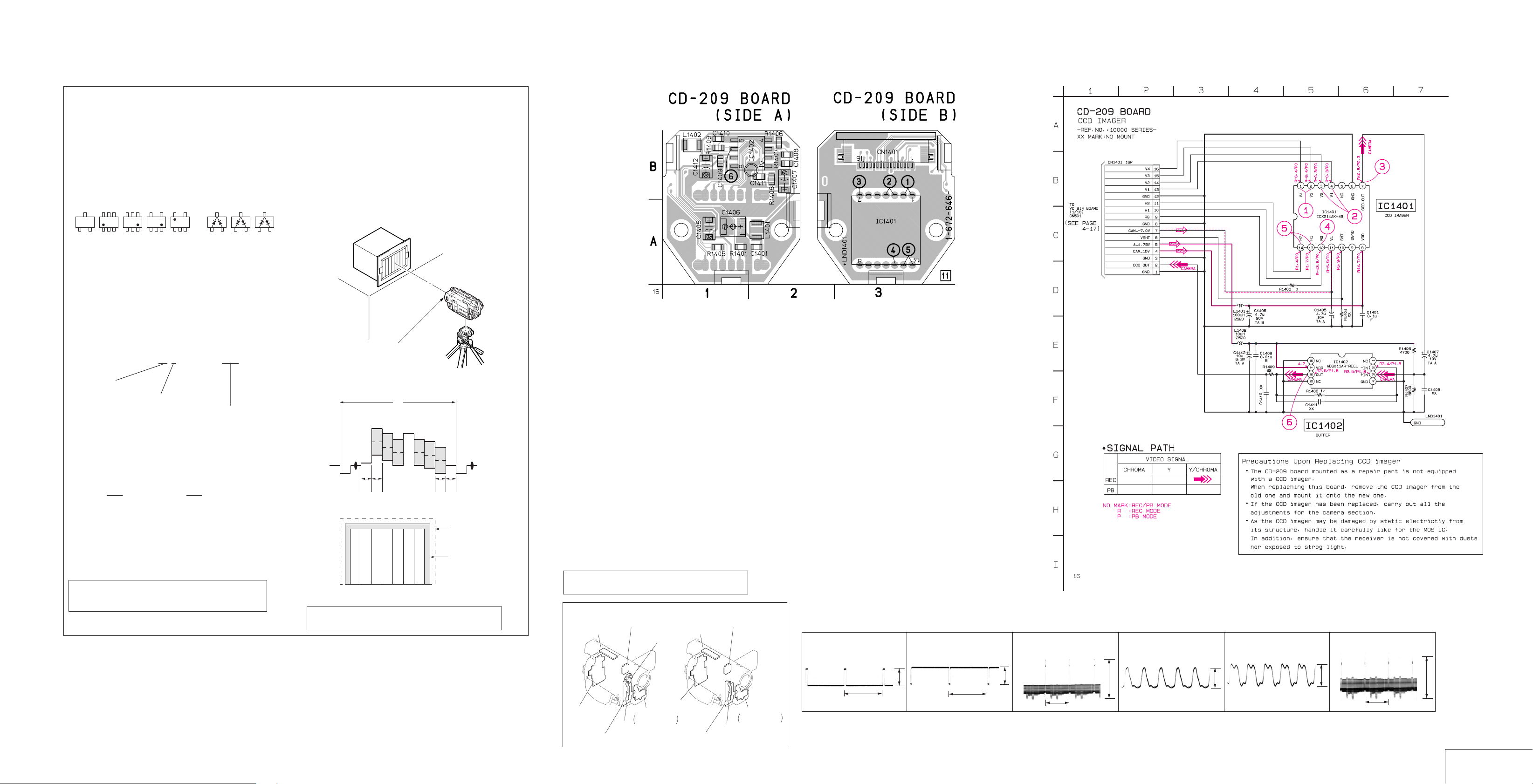
CD-209 BOARD
C1401 A-2
C1405 A-1
C1406 A-1
C1407 B-2
C1408 B-2
C1409 B-1
C1410 B-1
C1411 B-2
C1412 B-1
CN1401 A-3
IC1401 A-3
IC1402 B-2
L1401 A-2
L1402 B-1
R1401 A-1
R1405 A-1
R1406 B-2
R1407 B-2
R1408 B-2
R1409 B-1
CD-209 (CCD IMAGER) PRINTED WIRING BOARD
— Ref. No. CD-209 Board; 10,000 Series —
Kinds of capacitor
Temperature characteristics
External dimensions (mm)
• Constants of resistors, capacitors, ICs and etc with XX indicate
that they are not used.
In such cases, the unused circuits may be indicated.
• Parts with ★ differ according to the model/destination.
Refer to the mount table for each function.
• All variable and adjustab le resistors have characteristic curve B,
unless otherwise noted.
• Signal name
XEDIT→ EDIT PB/XREC → PB/REC
• 2 : non flammable resistor
• 1 : fusible resistor
• C : panel designation
• A : B+ Line
• B : B– Line
• J : IN/OUT direction of (+,–) B LINE.
• C : adjustment for repair.
• Circled numbers refer to w aveforms.
Note : The components identified by mark ! or dotted
line with mark ! are critical for safety.
Replace only with part number specified.
2. Adjust the distance so that the output waveform of Fig. a and
the Fig. b can be obtain.
H
Yellow
Cyan
White
Magenta
Green
Red
Blue
AABBA=B
Fig. a (Video output terminal output waveform)
Electron beam
scanned frame
Red
Cyan
White
Green
Yellow
Blue
Magenta
CRT picture frame
Fig.b (Picture on monitor TV)
When indicating parts by reference number, pleas include
the board name.
For printed wiring boards
• This board is six-layer print board. However, the patterns of layers two to five have not been included in
the diagram.
There are few cases that the part printed on this
diagram isn’t mounted in this model.
(TRV77E)(TRV66E)
VF-129
(B/W EVF)
CD-209
(CCD IMAGER)
VF-129
(B/W EVF)
CD-209
(CCD IMAGER)
VL-23
(VIDEO LIGHT)
CD-209
BOARD
CAMERA REC
1 IC1401 1,2
2 IC1401 3,4
3 IC1401 7
4 IC1401 !™
5 IC1401 !£,!¢
6 IC1402 6
6.8Vp-p
H
H
1.1Vp-p
14.187 MHz
3.3Vp-p
14.187 MHz
DD-117
(DC/DC CONVERTER)
SE-83
(STEADY SHOT)
MA-351
STEREO MIC AMP,
LASER LINK
PJ-92
(AV IN/OUT)
DD-117
(DC/DC CONVERTER)
SE-83
(STEADY SHOT)
PJ-92
(AV IN/OUT)
MA-351
STEREO MIC AMP,
LASER LINK
6.8Vp-p
H
4-7 4-8 4-9
3.7Vp-p
H
1.2Vp-p
CCD IMAGER
CD-209
Page 3
CCD-TRV66E/TRV77E
CCD-TRV66E/TRV77E
For schematic diagram
• Refer to page 4-11 for printed wiring board.
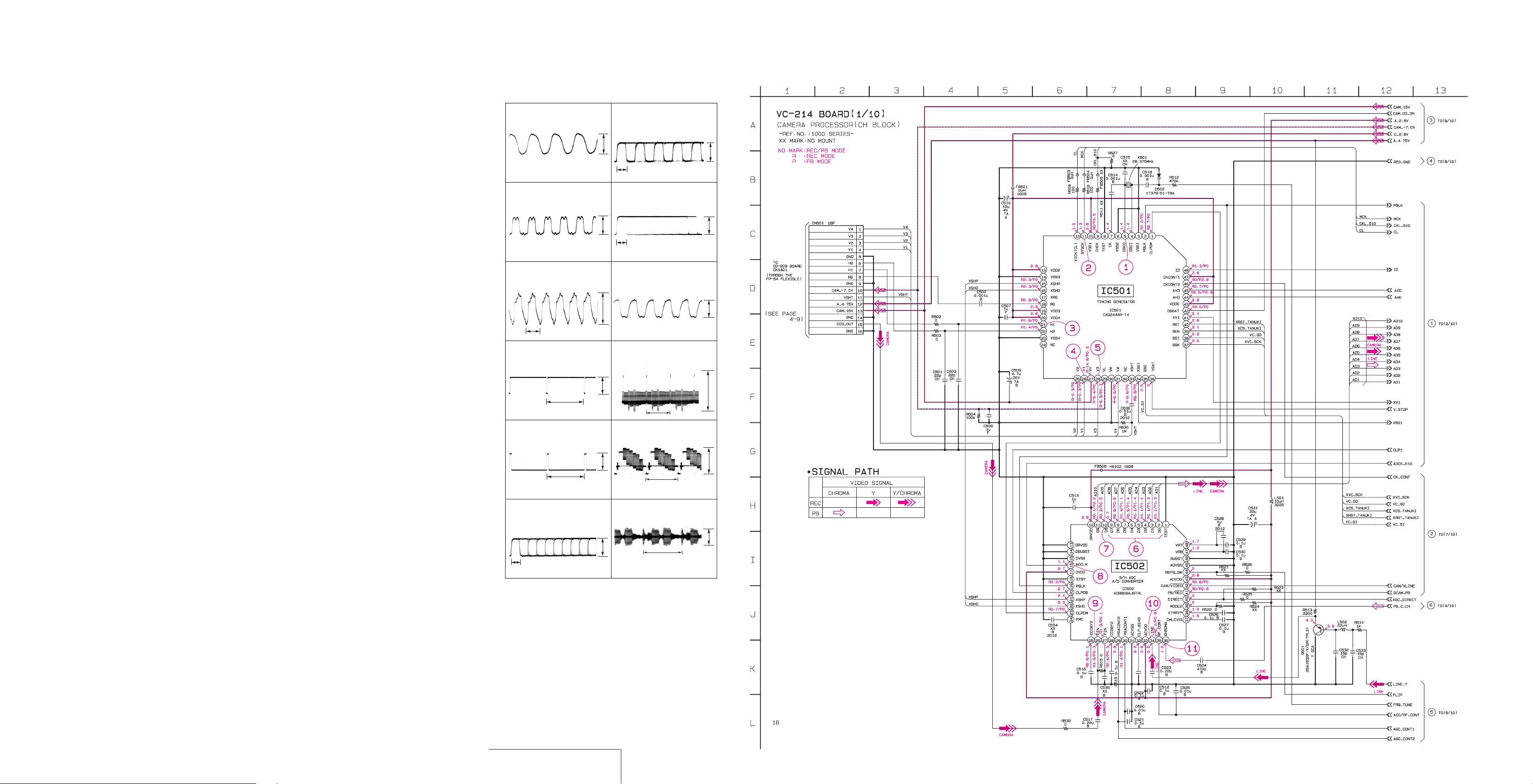
VC-214
1
CAMERA REC/PB
2
CAMERA REC/PB
3
CAMERA REC
4
CAMERA REC
BOARD (1/10)
IC501 5
28.374 MHz
IC501 !¡
14.187 MHz
IC501 @¡
50 nsec
IC501 @§
7
CAMERA REC
LINE REC
3.0Vp-p
7
3.0Vp-p
8
CAMERA REC/PB
LINE REC
3.0Vp-p
9
CAMERA REC
IC502 !º
72 nsec
IC502 !º PB
72 nsec
IC502 !§
14.187 MHz
IC502 @§
2.9Vp-p
2.9Vp-p
2.9Vp-p
H
5
IC501 @•
CAMERA REC
H
6
IC502 2 – 9
CAMERA REC/PB
LINE REC
72 nsec
7.0Vp-p
7.0Vp-p
2.9Vp-p
H
!º
IC502 #¢
LINE REC
!¡
IC502 #§ PB
1.2Vp-p
H
H
0.5Vp-p
0.3Vp-p
CAMERA PROCESSOR
VC-214 (1/10)
4-17 4-18
Page 4
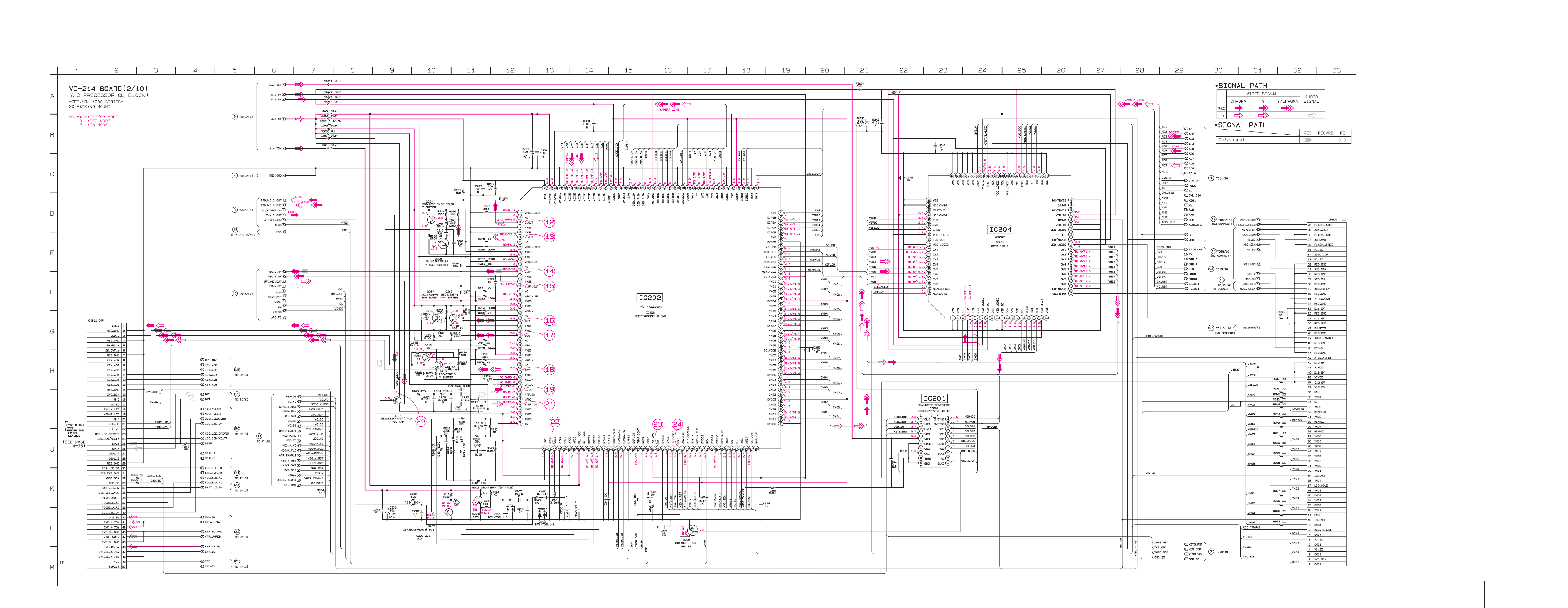
For schematic diagram
• Refer to page 4-11 for printed wiring board.
• Refer to page 4-23 for waveforms.
CCD-TRV66E/TRV77E
4-19 4-20 4-21 4-22
Y/C PROCESSOR
VC-214 (2/10)
Page 5
CCD-TRV66E/TRV77E
CCD-TRV66E/TRV77E
For schematic diagram
• Refer to page 4-11 for printed wiring board.
VC-214
!™
CAMERA REC/PB
!™
LINE REC
!£
CAMERA REC/PB
!£
LINE REC
BOARD (2/10)
IC202 3
H
IC202 3
H
IC202 6
H
IC202 6
0.45Vp-p
0.5Vp-p
0.8Vp-p
IC202 @£
!§
CAMERA REC/PB
H
!§
IC202 @£
LINE REC
H
!¶
IC202 @§
CAMERA REC/PB
H
!¶
IC202 @§
LINE REC
0.3Vp-p
0.3Vp-p
0.1Vp-p
IC202 #¶
!ª
LINE REC
H
@º
Q217 E
PB
H
@¡
IC202 $º
PB
0.1 µsec/div
@™
IC202 $¶
LINE REC/PB
0.3Vp-p
0.3Vp-p
0.4Vp-p
H
!¢
IC202 !£
CAMERA REC
H
!∞
IC202 !§
CAMERA REC
0.2 µsec
0.9Vp-p
!•
IC202 #£
CAMERA REC/PB
0.4Vp-p
!•
IC202 #£
LINE REC
0.4Vp-p
H
H
H
0.3Vp-p
@£
IC202 ^•
CAMERA REC/PB
1.0Vp-p
@¢
IC202 &™
CAMERA REC/PB
0.9Vp-p
13.325 MHz
14.187 MHz
25 Hz
3.0Vp-p
3.0Vp-p
2.8Vp-p
4-23
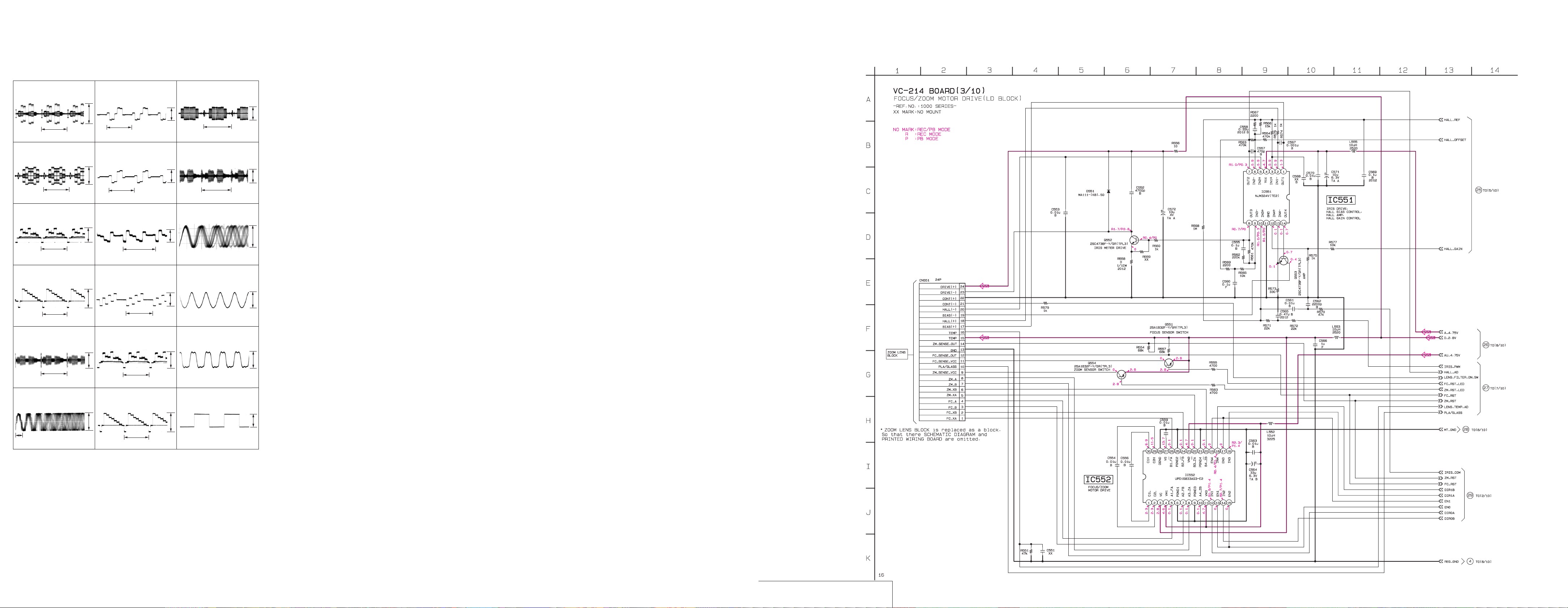
FOCUS/ZOOM MOTOR DRIVE
VC-214 (3/10)
4-25 4-26
Page 6
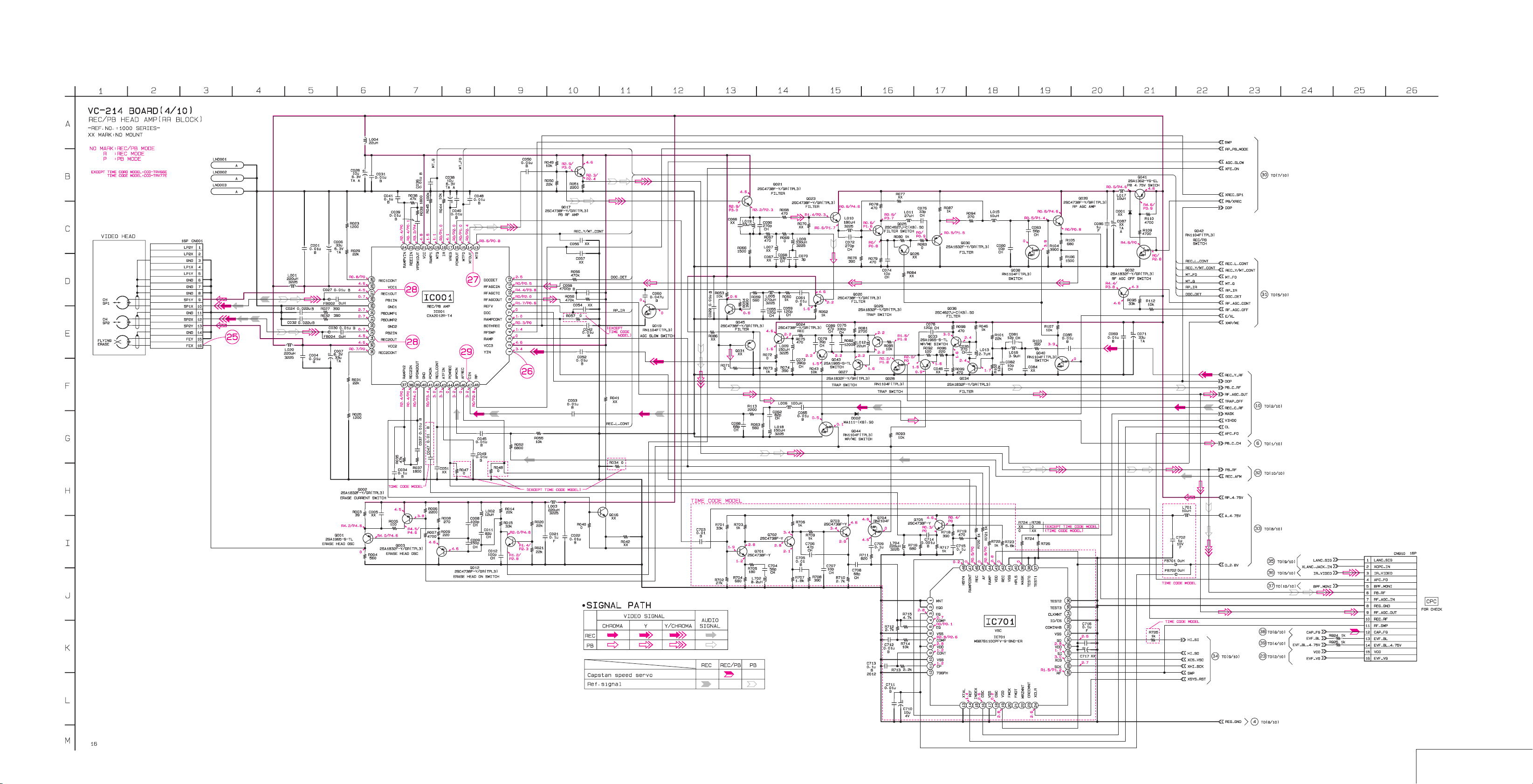
For schematic diagram
• Refer to page 4-11 for printed wiring board.
• Refer to page 4-30 for waveforms.
CCD-TRV66E/TRV77E
4-27 4-28 4-29
REC/PB HEAD AMP
VC-214 (4/10)
Page 7

CCD-TRV66E/TRV77E
For schematic diagram
• Refer to page 4-11 for printed wiring board.
VC-214
@∞
CAMERA REC
@§
CAMERA REC
@¶
PB
@•
CAMERA REC
BOARD (4/10)
CN001 !§, Q001 C
7.14 MHz
IC001 1
0.1 µsec/div
IC001 !¢
1 µsec/div, 0.2 V/div
IC001 @¶,#¢
9.0Vp-p
0.3Vp-p
VC-214
#º
CAMERA REC/PB
#º
LINE REC
#¡
CAMERA REC/PB
#¡
LINE REC
BOARD (5/10)
IC151 3
H
IC151 3
H
IC151 5
H
IC151 5
0.48Vp-p
0.5Vp-p
0.3Vp-p
#∞
IC151 @ª
CAMERA REC/PB
H
#§
IC151 #¶
LINE REC
17.7343 MHz
#¶
IC151 $¢
LINE REC
H
#•
IC151 $§
LINE REC
2Vp-p
0.26Vp-p
0.16Vp-p
0.2 µsec/div, 1 V/div
@ª
IC001 $¶
CAMERA REC
1 µsec/div, 0.1 V/div
H
#™
IC151 !¶
CAMERA REC/PB
H
#£
IC151 @∞
CAMERA REC/PB
H
#¢
IC151 @¶
CAMERA REC/PB
IR ON
H
0.4Vp-p
0.12Vp-p
0.06Vp-p
0.5Vp-p
#ª
IC151 ^º
LINE REC
$º
IC151 ^™
LINE REC
$¡
IC151 ^¢
LINE REC
H
H
H
H
0.52Vp-p
0.4Vp-p
0.48Vp-p
0.3Vp-p
VIDEO/INTERFACE
VC-214 (5/10)
4-30 4-31 4-32
Page 8

For schematic diagram
• Refer to page 4-11 for printed wiring board.
CCD-TRV66E/TRV77E
CCD-TRV66E/TRV77E
VC-214
$™
CAMERA REC/PB
$£
CAMERA REC/PB
IR ON
$¢
CAMERA REC/PB
IR ON
BOARD (6/10)
IC751 7
4.43 MHz
IC751 @™
0.5 µsec/div
IC751 $¡
H
0.2Vp-p
0.22Vp-p
0.22Vp-p
4-33 4-34
IR TRANSMITTER
VC-214 (6/10)
Page 9

CCD-TRV66E/TRV77E
For schematic diagram
• Refer to page 4-11 for printed wiring board.
VC-214
CAMERA REC/PB
$∞
$§
BOARD (7/10)
IC402 1
20.0 MHz
IC402 $¶
25 Hz
1.7Vp-p
2.8Vp-p
MODE CONTROL
VC-214 (7/10)
4-37 4-384-36
Page 10

CCD-TRV66E/TRV77E
For schematic diagram
• Refer to page 4-11 for printed wiring board.
VC-214
CAMERA REC/PB
$¶
$•
$ª
BOARD (8/10)
IC801 1,2,@ª
150 Hz
IC801 !¡
25 Hz
IC801 !•
150 Hz
FP-249 (S/T REEL SENSOR), FP-356 (TOP SENSOR), FP-355 (TAPE LED) FLEXIBLE BOARD
PRINTED WIRING BO ARD
— Ref. No. FP-249, 356, 355 FLEXIBLE board; 5,000 series —
1.2Vp-p
2.8Vp-p
2.8Vp-p
%º
IC802 7
%¡
IC802 9
1.0 msec/div
10.3 µsec
100mV
0.1Vp-p
4-39 4-40 4-41
SERVO
VC-214 (8/10)
S/T REEL SENSOR, TOP SENSOR, TAPE LED
/
FP-249, FP-356, FP-355
Page 11

CCD-TRV66E/TRV77E
VL-23 (VIDEO LIGHT) PRINTED WIRING BOARD (TRV66E only)
— Ref. No. VL-23 Board; 2,000 Series —
VC-214
BOARD (9/10)
CAMERA REC/PB
%™
IC604 $º
20.0 MHz
%£
IC604 %£
32.768 KHz
For schematic diagram
• Refer to page 4-11 for printed wiring board.
3.2Vp-p
3.2Vp-p
For printed wiring boards
• Chip parts
Transistor
C
BE
There are few cases that the part printed on this
diagram isn’t mounted in this model.
(TRV66E)
VF-129
(B/W EVF)
DD-117
(DC/DC CONVERTER)
SE-83
(STEADY SHOT)
CD-209
(CCD IMAGER)
MA-351
STEREO MIC AMP,
LASER LINK
PJ-92
(AV IN/OUT)
VL-23
(VIDEO LIGHT)
VL-23 BOARD
C151 A-2
C152 A-4
C153 A-2
CN151 A-3
D151 A-4
D152 A-2
D153 A-2
L151 A-2
Q151 A-2
Q152 A-4
R151 A-4
R152 A-2
R153 A-2
R154 A-3
VIDEO LIGHT
VL-23
HI CONTROL
/
VC-214 (9/10)
4-43 4-44 4-45 4-46
Page 12

For schematic diagram
• Refer to page 4-11 for printed wiring board.
CCD-TRV66E/TRV77E
4-47 4-48 4-49
AUDIO
VC-214 (10/10)
Page 13

CCD-TRV66E/TRV77E
4-53 4-54
STEADY SHOT
SE-83
AV IN/OUT
/
PJ-92
Page 14

CCD-TRV66E/TRV77E
4-57 4-58 4-59
STEREO MIC AMP, LASER LINK
MA-351
Page 15

CCD-TRV66E/TRV77E
CCD-TRV66E/TRV77E
PD-105
CAMERA REC/PB
1
2
3
4
BOARD (1/2)
IC5801 2
23.78 KHz
IC5502 8
H
IC5502 9
H
IC5502 !º
3.0Vp-p
0.4Vp-p
0.3Vp-p
5
IC5502 @º
6
IC5502 @™
7
IC5502 @¢
H
2H
2H
2H
0.1Vp-p
2.0Vp-p
2.0Vp-p
2.0Vp-p
4-63 4-64
RGB DECODER, LCD
PD-105 (1/2)
4-65
Page 16

CCD-TRV66E/TRV77E
CCD-TRV66E/TRV77E
For schematic diagram
• Refer to page 4-60 for printed wiring board.
PD-105
CAMERA REC/PB
8
9
!º
BOARD (2/2)
IC5601 @§
5.48 MHz
IC5601 #¶
IC5602 7
6.7 KHz
3.0Vp-p
2.8Vp-p
H
5.0Vp-p
4-66
TIMING GENERATOR, BACK LIGHT DRIVE
PD-105 (2/2)
4-67 4-68
Page 17

VF-129 (B/W EVF) PRINTED WIRING BOARD
CD-209
(CCD IMAGER)
(TRV77E)(TRV66E)
VL-23
(VIDEO LIGHT)
MA-351
STEREO MIC AMP,
LASER LINK
PJ-92
(AV IN/OUT)
SE-83
(STEADY SHOT)
DD-117
(DC/DC CONVERTER)
VF-129
(B/W EVF)
CD-209
(CCD IMAGER)
MA-351
STEREO MIC AMP,
LASER LINK
PJ-92
(AV IN/OUT)
SE-83
(STEADY SHOT)
DD-117
(DC/DC CONVERTER)
VF-129
(B/W EVF)
— Ref. No. VF-129 Board; 3,000 Series —
VF-129 BOARD
C901 A-3
C902 A-3
C903 A-2
C904 B-2
C905 A-3
C906 A-2
C907 A-1
C908 C-2
C909 B-1
C910 C-3
C911 C-3
C912 B-3
C913 A-2
C914 D-3
C915 E-3
C916 C-3
CN901 B-3
CN902 B-1
D901 A-1
D903 D-3
IC901 A-1
L901 B-1
L902 B-3
L903 D-1
Q901 A-2
Q902 B-2
Q903 C-3
Q904 C-2
R901 A-3
R902 A-3
R903 A-1
R904 A-3
R905 A-2
R906 A-2
R907 B-1
R908 B-2
R909 B-2
R910 B-2
R911 A-3
R912 A-2
R913 C-2
R914 C-2
R915 B-1
R916 A-1
R917 A-1
R918 C-2
R919 C-2
R920 C-2
R921 D-2
R922 E-1
R923 E-3
R924 C-3
R925 C-3
R926 D-2
R927 B-1
R928 B-1
R929 A-1
R930 C-1
R931 C-1
R932 C-1
RV903 C-2
RV904 D-1
T901 D-1
T902 D-1
TH901 B-2
W901 D-2
CCD-TRV66E/TRV77E
VF-129
CAMERA REC/PB
1
2
3
4
BOARD
IC901 1,5
2.0Vp-p
20 msec
IC901 3
2.0Vp-p
20 msec
IC901 7
1.1Vp-p
20 msec
IC901 !¡
For printed wiring boards
• Chip parts
Transistor
C
BE
5
IC901 !£
6
IC901 !§
H
0.9Vp-p
1.1Vp-p
H
2.4Vp-p
H
There are few cases that the part printed on this
diagram isn’t mounted in this model.
4-69 4-70 4-71
B/W EVF
VF-129
Page 18

CCD-TRV66E/TRV77E
4-75 4-76 4-77
USER CONTROL
CF-56/MR-8500
Page 19

CCD-TRV66E/TRV77E
DD-117
CAMERA REC/PB
1
2
BOARD
IC801 4
2 µsec
IC801 ^¢
2 µsec
0.75Vp-p
0.75Vp-p
4-81 4-82 4-83 4-84
DC/DC CONVERTER
DD-117
Page 20

CCD-TRV66E/TRV77E
CCD-TRV66E/TRV77E
CONTROL SWITCH BLOCK
FK-8500/SS-8500
4-88E
 Loading...