

Page 1

BC05 Module Spec.
Shenzhen Synchron Electronics Co.,Ltd. 2010.11
1.General Description and Spcification
1.1 General Description
This product is a Class 2 SMT Bluetooth Module used CSR BC5-MultiMedia
External. It provides data and voice communications. It interfaces with a host through
USB or UART and support data rate up to 12M/3Mbps.
General Fetures:
■
Class 2 Bluetooth Module
■
Bluetooth Spec. V2.1+EDR Compliant
■
Support Firmware Upgrade
■
USB 2.0 and UART Host Interface
■
Multi-Configurable I2S, PCM or SPDIF Interface
■
Integrated 1.5V and 1.8V Linear Regulators
■
Integrated Switched-mode Regulator
■
Integrated Battery Charger
■
Integrated Microphone bias& LED Driver
■
64MIPS Kalimba DSP Co-processor
■
Built in 16-bit Stereo Codec- 95dB SNR for DAC
■
Enhanced Audibility and Noise Cancellation
■
Support for 802.11 Co-existence
■
Green (RoHS Compliant)
1.2 Device Details
Radio
■ Common TX/RX terminal simplifies external matching; eliminates external antenna switch
■ BIST minimises production test time
■ Bluetooth v2.1 + EDR specification compliant
Transmitter
■ 4dBm RF transmit power with level control from onchip 6-bit DAC over a dynamic range >30dB
■ Class 2 and Class 3 support without the need for an external power amplifier or TX/RX switch
Page 2

Receiver
■ Receiver sensitivity of -70dBm
■ Integrated channel filters
■ Digital demodulator for improved sensitivity and cochannel rejection
■ Real-time digitised RSSI available on HCI interface
■ Fast AGC for enhanced dynamic range
Baseband and Software
■ 16Mbit external Flash
■ 48Kbyte internal RAM, allows full-speed data transfer, mixed voice/data and full piconet support
■ Logic for forward error correction, header error control, access code correlation, CRC,
demodulation, encryption bit stream generation, whitening and transmit pulse shaping
■ Transcoders for A-law, μ-law and linear voice from host and A-law, μ-law and CVSD voice
over air
Physical Interfaces
■ SPI with clock speeds up to 64MHz in Master mode and 32MHz in Slave mode
■ I2C master compatible interface
■ UART interface with programmable data rate up to 3Mbits/s with an optional bypass mode
■ USB v2.0 interface
■ Bi-directional serial programmable audio interface supporting PCM, I2S and SPDIF formats
■ Two LED drivers with faders
Kalimba DSP
■ Very low power Kalimba DSP co-processor, 64MIPS, 24-bit fixed point core
■ SBC decode takes approximately 4mW power consumption while streaming music
■ Single-cycle MAC; 24 x 24-bit multiply and 56-bit accumulator
■ 32-bit instruction word, dual 24-bit data memory
■ 6K x 32-bit program RAM, 16K x 24-bit + 12K x 24- bit data RAM
■ 64-word x 32-bit program memory cache when executing from Flash
Stereo Audio Codec
■ 16-bit internal stereo codec
■ Dual ADC and DAC for stereo audio
■ Integrated amplifiers for driving 16Ω speakers; no need for external components
■ Support for single-ended speaker termination and line output
■ Integrated low-noise microphone bias
■ ADC sample rates are 8, 11.025, 16, 22.05, 32 and 44.1kHz
Page 3

■ DAC sample rates are 8, 11.025, 12, 16, 22.05, 24, 32, 44.1 and 48kHz
Auxiliary Features
■ Power management includes digital shutdown and wake-up commands with an integrated
low-power oscillator for ultra-low power Park/Sniff/Hold mode
■ On-chip regulators: 1.5V output from 1.8V to 2.7V input and 1.8V output from 2.7V to 4.5V input
■ On-chip high-efficiency switched-mode regulator; 1.8V output from 2.7V to 4.4V input
■ Power-on-reset cell detects low supply voltage
■ 10-bit ADC and 8-bit DAC available to applications
■ On-chip charger for lithium ion/polymer batteries
1.3 Specification
Chipset CSR BC05 Multimedia
Specification Version Bluetooth V2.1+EDR
Power Class Class 2
Frequency Band 2400~2483.5MHz
Max. Tx Power -6~+4dBm
<
RX Sensitivity
-70dBm
Distance >10m(No obstacle)
Flash Size 16M
Power Voltage 3.3V
Supply Current <40mA
Operation Temperature
Dimension 32mm(L)x 13.5 mm(W) x 1.2mm(H)
-10 ~ +45 ℃
Page 4
2.Package Information
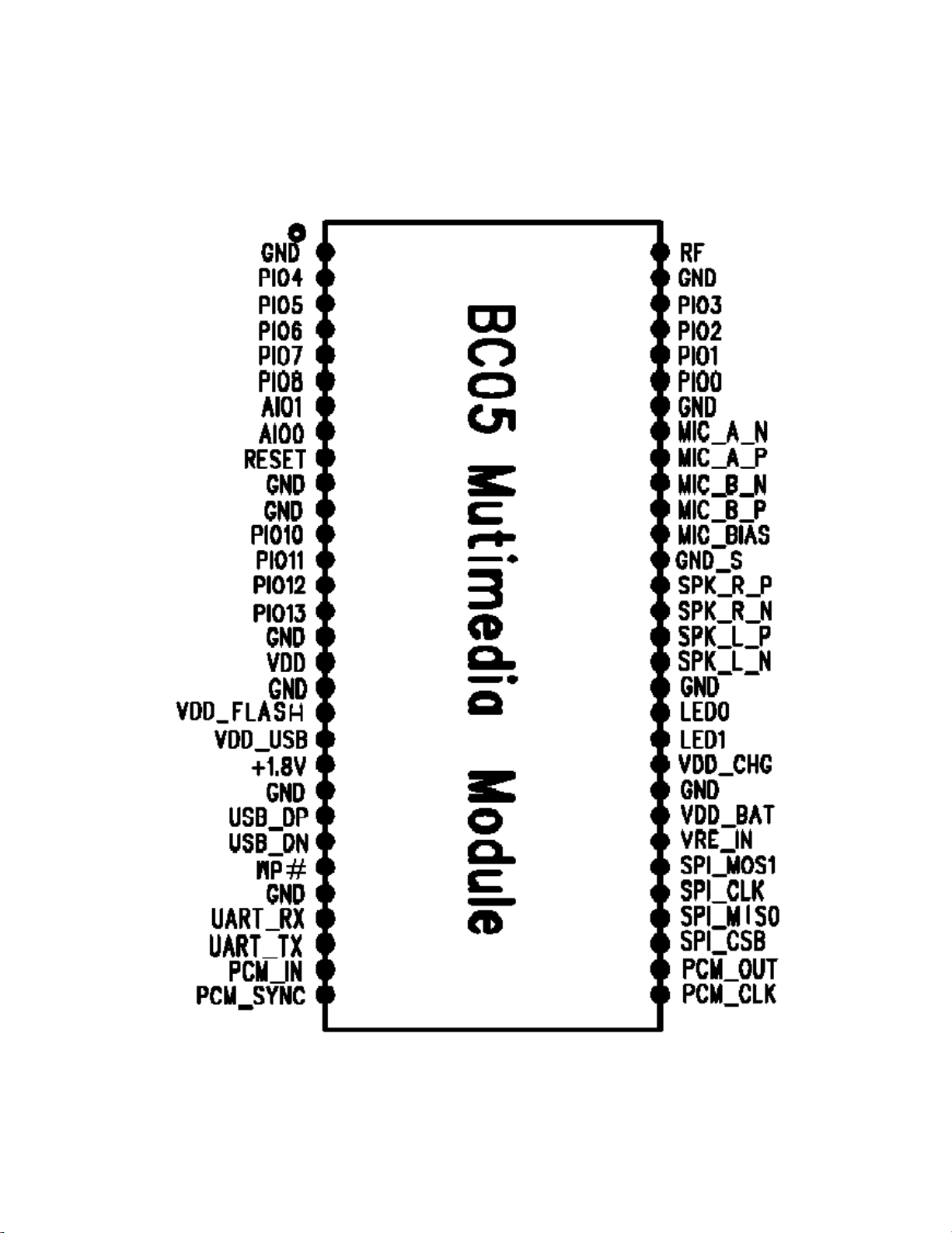
2.1 Pinout Diagram
Figure 1: BC05 Module Pinout(Top View)
Page 5

2.2 Terminal Functions
Pin Name Pin Number Description
GND 1 Ground
PIO4 2
PIO5 3
PIO6 4
Programmable input/output line
PIO7 5
PIO8 6
AIO1 7
Analogue programmable input/output
AIO0 8
RESET 9 System Reset(Low Active)
GND 10 Ground
GND 11
PIO10 12
Ground
PIO11 13
Programmable input/output line
PIO12 14
PIO13 15
GND 16
Ground
Positive supply for SPI/PCM ports and PIO[15:4]
VDD
17
and BC05 MM Flash Pads, Connect to 3.3V
GND 18 Ground
VDD_Flash 19
VDD_USB 20
Positive supply for Flash Memory ,Connect to 3.3V
Positive supply for UART/USB ports
+1.8V 21 Switch-mode power regulator output
GND 22 Ground
USB data plus with selectable internal 1.5k Ω
USB_DP 23
pull-up resistor
USB_DN 24
USB data minus
WP# 25 Flash write protect(Low Active)
GND 26 Ground
UART_RX 27
UART_TX 28
UART data input
UART data output
PCM_IN 29 Synchronous data input
PCM_SYNC 30 Synchronous data sync
PCM_CLK 31
PCM_OUT 32
Synchronous data clock
Synchronous data output
SPI_CSB 33 Chip select for SPI, active low
Page 6

SPI_MOSO 34
Lithium ion/polymer battery positive terminal.
mode
SPI data output
SPI_CLK 35 SPI clock
SPI_MOSI 36 SPI data intput
VRE_IN 37
Take high to enable high-voltage linear regulator
and switch-mode regulator
VDD_BAT 38
Battery charger output and input to switch-
regulator
GND 39 Ground
VDD_CHG 40 Battery charge
LED1 41
LED Driver
LED0 42
GND 43 Ground
SPK_L_N 44 Speaker output negative, left
SPK_L_P 45
SPK_R_N 46
Speaker output positive, left
Speaker output negative, right
SPK_R_P 47 Speaker output positive, right
GND_S 48 Signal Ground
MIC_BIAS 49
MIC_B_P 50
Microphone bias
Microphone input positive, right
MIC_B_N 51 Microphone input negative, right
MIC_A_P 52 Microphone input positive, left
MIC_A_N 53
GND 54
Microphone input negative, left
Ground
PIO0 55
PIO1 56
Programmable input/output line
PIO2 57
PIO3 58
GND 59 Ground
RF 60 Transmitter output/switched receiver input
Page 7

2.3 Package Dimensions
Figure 2: BC05 Module package Dimensions
Page 8

3.Hardware Description
3.1 Block Diagram
Figure 3: BC05 Module Block Diagram
Page 9

3.2 RF Ports
Figure 4: RF Ports Diagram
RF_N and RF_P form a complementary balanced pair and are available for both
transmit and receive. On transmit their outputs are combined using an external balun
into the single-ended output required for the antenna. Similarly, on receive their input
signals are combined internally. Both terminals present similar complex impedances
that may require matching networks between them and the balun.
An LC network, L4 and C17. This provides a DC bias for the BlueCore5-MM
from the 1.5V rail.
The BPF1 used to suppress the signal out of Bluetooth Frequency Band and
enhance the EMC capacity.
The DC level must be set at VDD_RADIO.
3.3 UART Ports
BC05 Module UART interface provides a simple mechanism for communicating
with other serial devices using the RS232 protocol. When BlueCore5‑Multimedia
External is connected to another digital device, UART_RX and UART_TX transfer
data between the two devices.
The Baud rate of the UART ports:
Baud rate
Minimum
Maximum
1200 baud (≤2%Error)
9600 baud (≤1%Error)
4Mbaud (≤1%Error)
Page 10

3.4 USB Ports
This is a full speed (12Mbits/s) USB interface for communicating with other
compatible digital devices.BC05 Module acts as a USB peripheral, responding to
requests from a master host controller such as a PC.
As USB is a master/slave oriented system (in common with other USB
peripherals), BlueCore5‑Multimedia External only supports USB Slave operation.
4. Green Products and RoHS Compliance
5. Reference
1) BlueCore5-Multimedia External Product Data Sheet, CS-101568-DSP4 (bc05-ds-
004P)
2) Specification of the Bluetootn System , Verion 2.1+EDR
Page 11

COMPLIANCES
Federal Communication Commission Interference
Statement
This equipment has been tested and found to comply with the limits for a Class B
digital device, pursuant to Part 15 of the FCC Rules. These limits are designed to
provide reasonable protection against harmful interference in a residential
installation. This equipment generates, uses and can radiate radio frequency
energy and, if not installed and used in accordance with the instructions, may
cause harmful interference to radio communications. However, there is no
guarantee that interference will not occur in a particular installation. If this
equipment does cause harmful interference to radio or television reception, which
can be determined by turning the equipment off and on, the user is encouraged to
try to correct the interference by one of the following measures:
• Reorient or relocate the receiving antenna.
• Increase the separation between the equipment and receiver.
• Connect the equipment into an outlet on a circuit different from that to which the
receiver is connected.
• Consult the dealer or an experienced radio/TV technician for help.
This device complies with Part 15 of the FCC Rules. Operation is subject to the
following two conditions: (1) This device may not cause harmful interference, and
(2) this device must accept any interference received, including interference that
may cause undesired operation.
FCC Caution: Any changes or modifications not expressly approved by the party
responsible for compliance could void the user's authority to operate this
equipment.
Page 12

IMPORTANT NOTE:
FCC Radiation Exposure Statement:
This equipment complies with FCC radiation exposure limits set forth for an
uncontrolled environment. This equipment should be installed and operated with
minimum distance 20cm between the radiator & your body.
This transmitter must not be co-located or operating in conjunction with any other
antenna or transmitter.
COMPLIANCES
ii
IC Statement
This device complies with RSS-210 of the Industry Canada Rules.
Operation is subject to the following two conditions:
1) this device may not cause interference and
2) this device must accept any interference, including interference that may cause
undesired operation of the device
Cet appareil est conforme aux normes RSS sans licenced's Industry Canada. Le fonctionnement est soumis aux deux conditions
suivantes : (1) cet appareil ne doit pas provoquer d' interf'erence, et (2) cet appareil doit accepter toutes les interf'erences, y compris
celles susceptibles de de'clencher le fonctionnement involontaire de l'appareil.
This Class B digital apparatus complies with Canadian ICES-003.
Cet appareil numerique de la class B est conforme a la norme NMB-003 du
Canada.
IMPORTANT NOTE:
IC Radiation Exposure Statement:
This equipment complies with Canada radiation exposure limits set forth for
uncontrolled environments. This equipment should be installed and operated with
minimum distance 20cm between the radiator & your body.
This transmitter must not be co-located or operating in conjunction with any other
antenna or transmitter.
The
end host device use this module should marked "Contain FCC ID:AK8BTMS1"or "Contains Transmitter Module IC:409B-BTMS1"
in the label of the host device.
 Loading...