


Rhein Tech Laboratories, Inc. Client: Sony Ericsson Mobile Communications
360 Herndon Parkway Model: CM-52 (0.6W)
Suite 1400 Standards: FCC Pt 22, 24/IC RSS-129/-133
Herndon, VA 20170 Report Number: 2005084
http://www.rheintech.com
Date: August 3, 2005
APPENDIX I: USER MANUAL
Please refer to the following pages.
56 of 61

Confidential
USERS MANUAL
Document number Revision
4/198 17-LXE 108 566 Uen PA6
CM52 Integrator's Manual
1(41)

Confidential
USERS MANUAL
Document number Revision
4/198 17-LXE 108 566 Uen PA6
2(41)
Table of Contents
1 Introduction to the Integrator’s Manual 5
1.1 OVERVIEW 5
1.2 HOW TO READ THE MANUAL 5
1.3 SERVICE AND SUPPORT 5
1.3.1 WEB PAGES 5
1.4 RELATED DOCUMENTS 6
1.5 ABBREVIATIONS 6
2 Integrating the CM52 Module 7
2.1 OVERVIEW 7
2.2 MECHANICAL DESCRIPTION 7
2.2.1 MECHANICAL DIMENSIONS 8
2.2.2 HEAT-SINK REQUIREMENTS 9
2.2.3 MOUNTING HOLES 9
2.3 SYSTEM CONNECTOR INTERFACE 10
2.3.1 MECHANICAL OVERVIEW 10
2.3.2 PINOUT 11
2.3.3 LOGIC LEVELS 12
2.4 POWER SUPPLY 12
2.4.1 POWER SUPPLY AND GROUND SIGNALS 12
2.4.1.1 POWER SUPPLY SIGNAL PINS 12
2.4.1.2 GROUND SIGNAL PINS 13
2.4.2 POWER CONSUMPTION 13
2.4.2.1 WAKEUP-INRUSH CURRENT 16
2.4.2.2 CONTACT-INRUSH CURRENT 16
2.4.2.3 POWER DOWN MODE (MINIMUM DC POWER CONSUMPTION) 16
2.4.3 VREF REQUIREMENTS 16
2.4.4 REAL TIME CLOCK (RTC) CIRCUIT 17
2.5 AUDIO INTERFACE 17
2.5.1 DIGITAL AUDIO 18
2.5.1.1 DATA FORMAT 18
2.5.1.2 TIMING 18
2.5.2 ANALOG AUDIO 20
2.6 SERIAL DATA INTERFACE 23
2.7 ANTENNA INTERFACE 24
2.7.1 ANTENNA CONNECTOR 24
2.7.2 RF OUTPUT POWER 26
2.7.3 CARRIER APPROVAL 26
2.7.4 ANTENNA DIAGNOSTICS 26
3 Recommended Circuitry 28
3.1 STATUS GROUP RECOMMENDED CIRCUITRY 28
3.1.1 MODULE_PWR_EN_B 29
3.1.2 VREF 29
3.1.3 HW_SD 29
3.2 DATA GROUP RECOMMENDED CIRCUITRY 30
3.2.1 VPPFLASH/DCD 31
3.3 PCMGROUP RECOMMENDED CIRCUITRY 32
3.4 ANALOG AUDIO GROUP RECOMMENDED CIRCUITRY 33
3.4.1 CREATING AN ANALOG GROUND 33
3.4.2 CREATING AN ANALOG REFERENCE VOLTAGE (BIAS) 33
3.4.3 ANALOG GROUND VS. AGND 34
3.4.4 MICROPHONE PATH 34
3.4.5 LOUDSPEAKER PATH 35
3.5 SYSTEM CONNECTOR IO FUNCTIONALITY 36

Confidential
USERS MANUAL
Document number Revision
4/198 17-LXE 108 566 Uen PA6
3(41)
4 Functional Description 39
5 Hints for Integrating the Module 39
5.1 PRECAUTIONS 39
5.2 WHERE TO INSTALL THE MODULE 39
5.3 SAFETY STANDARDS 39
5.4 ANTENNA 40
5.4.1 ANTENNA TYPE 40
5.4.2 ANTENNA PLACEMENT 40
5.5 POSSIBLE COMMUNICATION DISTURBANCES 40
6 Technical Data 41

Confidential
USERS MANUAL
Document number Revision
4/198 17-LXE 108 566 Uen PA6
Tables
4(41)
TABLE 1
T
T
T
T
T
T
T
T
T
T
T
T
T
T
T
T
T
: S
YSTEM CONNECTOR AND MATING PART NUMBERS.
ABLE 2: PIN-OUT OF THE SYSTEM CONNECTOR HEADER ..............................................................................................................11
ABLE 3: CMOS OUTPUT / INPUT ELECTRICAL CHARACTERISTICS ................................................................................................12
ABLE 4: CM52 POWER SUPPLY REQUIREMENTS..........................................................................................................................12
ABLE 5: CM52 POWER SUPPLY SIGNALS....................................................................................................................................13
ABLE 6: CM52 GROUND SIGNALS...............................................................................................................................................13
ABLE 7: VCC_AUX SUPPLY POWER CONSUMPTION ...................................................................................................................14
ABLE 8: VCC_MAIN SUPPLY POWER CONSUMPTION..................................................................................................................15
ABLE 9: VREF SUPPLY DETAILS.................................................................................................................................................16
ABLE 10: CM52 AUDIO SIGNALS.................................................................................................................................................17
ABLE 11: CM52 DIGITAL AUDIO SIGNALS....................................................................................................................................18
ABLE 12: PCM TIMING PARAMETERS..........................................................................................................................................19
ABLE 13: CM52 ANALOG AUDIO SIGNALS...................................................................................................................................20
ABLE 14: AUDIO CHARACTERISTICS ............................................................................................................................................20
ABLE 15: SERIAL DATA CHANNELS .............................................................................................................................................23
ABLE 16: MOBILE STATION NOMINAL ANALOG POWER LEVELS....................................................................................................26
ABLE 17: MOBILE STATION CDMA MAXIMUM OUTPUT POWER ....................................................................................................26
ABLE 18: PIN DIRECTION FOR GENERAL PURPOSE SIGNALS.........................................................................................................38
.......................................................................................................10
Figures
FIGURE 1: CM52 PRIMARY SIDE .....................................................................................................................................................7
IGURE 2: CM52 SECONDARY SIDE ................................................................................................................................................7
F
IGURE 3: MECHANICAL DIMENSIONS DRAWING...............................................................................................................................8
F
IGURE 4: 40-PIN SYSTEM CONNECTOR........................................................................................................................................10
F
IGURE 5: 40-PIN SYSTEM CONNECTOR PIN NUMBERING...............................................................................................................10
F
IGURE 6: RTC FUNCTIONAL BLOCK DIAGRAM .............................................................................................................................17
F
IGURE 8: PCM TIMING DIAGRAM.................................................................................................................................................19
F
IGURE 9: COLOR AND KEYING FOR VARIOUS FAKRA CONNECTORS .............................................................................................24
F
IGURE 10: ANTENNA DIAGNOSTIC CIRCUIT...................................................................................................................................27
F
Revision History
Release Date Summary of Changes
PA1 05/07/2004 Initial Draft
PA2 09/01/2004 Formatting
PA3 11/17/2004 Updated Chapters 1 & 2
PA4 11/29/2004 Updated with reviewfeedback
PA5 12/1/2004 Updated the List of Tables and Figures
PA6 06/16/2005 Current Consumption Table, RTC Block Diagram, Mechanical Drawing

Confidential
USERS MANUAL
Document number Revision
4/198 17-LXE 108 566 Uen PA6
1 Introduction to the Integrator’s Manual
1.1 Overview
This manual is for use as a guide to the setup, installation, and use of the CM52 module
into your application. The module may be tested using the developer’s board, which is
supplied together with all the necessary tools in the Developer’s Kit.
1.2 How to read the manual
This manual is divided into six chapters:
Chapter 1 gives a general view of the integrator’s manual. A list of related documents
as well as a list of abbreviations, used throughout the manual, is also included.
Information concerning service and support is also presented.
Chapter 2 focuses on helping the hardware developer to integrate the CM52 hardware
into their application. An overview of the mechanical and electrical information is
provided. Also, interface specifications, RF output power, and power supply issues are
included in this chapter.
5(41)
Chapter 3 contains information on recommended circuitry needed to ensure proper
performance from the CM52 module.
Chapter 4 describes several of the common cellular functions available with the CM52.
Chapter 5 provides some hints for integrating the module.
Chapter 6 provides a summary of the technical data for the CM52 module.
1.3 Service and Support
1.3.1 Web Pages
Please look at our web page for more information about where you can buy our
modules or for recommendations of accessories and components. The address is:
http://www.sonyericsson.com/m2m
To register for product news and announcements or for product questions, contact the
Sony Ericsson modules technical support group:
• Telephone: 919-472-1122
• Email: M2Msupport.Americas@sonyericsson.com

1.4 Related Documents
CM52 AT Command Manual – Details the AT command interface for the CM52
The CM52 is based upon the following mobile standards:
•
IS-2000 Release 0 (1XRTT), MOB_P_REV – CDMA protocol
•
TIA/EIA/IS-91 – Mobile Station – Base Station Compatibility Standard for 800
MHz Analog Cellular
•
TIA/EIA-98-D – Recommended Minimum Performance Standards for Dual-Mode
Spread Spectrum Mobile Stations
1.5 Abbreviations
AGND Analog Reference
AMPS Advanced Mobile Phone System
AT Attention Command
CDMA Code Division Multiple Access
CTS Clear to Send
DCD Data Carrier Detect
DFMS Data from Mobile Station
DTMS Data to Mobile Station
DTR Data Terminal Ready
EMI Electromagnetic Interference
ESD Electrostatic Discharge
GND Chassis GrouND
IRA International Reference Alphabet
LSB Least Significant Bit
ME Mobile Equipment
MO Mobile Originated
MS Mobile Station
MT Mobile Terminated
OEM Original Equipment Manufacturer
PCB Printed Circuit Board
PCM Pulse Code Modulation
PIN Personal Identification Number
RD Receive Data, also known as DFMS
RF Radio Frequency
RTS Request to Send
SMS Short Message Service
TD Transmit Data, also know as DTMS
Confidential
USERS MANUAL
Document number Revision
4/198 17-LXE 108 566 Uen PA6
6(41)
Confidential
USERS MANUAL
Document number Revision
4/198 17-LXE 108 566 Uen PA6
2 Integrating the CM52 Module
2.1 Overview
The CM52 is a dual band, dual mode CDMA transceiver module. It operates in the 800
MHz band for CDMA and AMPS and in the 1900 MHz band for CDMA. It is designed
for consumer and OEM industrial voice and data applications.
The CM52 module is intended for mounting into an application developer’s chassis to
provide wireless communication capability for the product. The target chassis could be
in a wide variety of forms such as a residential electric meter, a point of sale terminal,
an alarm panel, or an automobile console. All initial configuration, mode control, and
operational commands are issued to the module over an RS-232 serial port using a
flexible AT command format. The module circuitry has been designed to meet the
environmental requirements of a large range of commercial and industrial users.
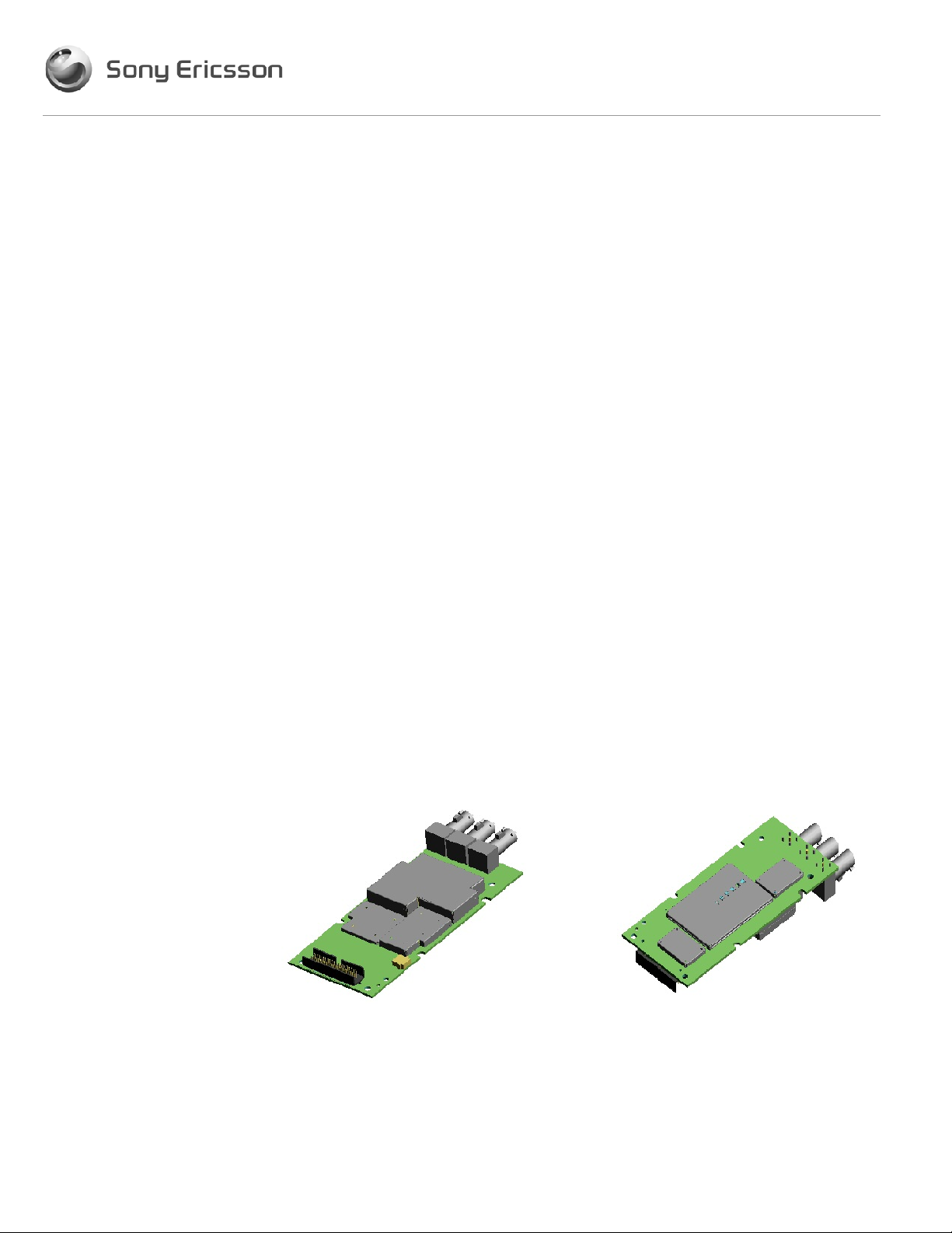
2.2 Mechanical Description
7(41)
The CM52 has no mechanical elements other than the main PCB assembly. All critical
electronic components are shielded using six cans to prevent internal and external
electromagnetic interference from degrading the module’s performance and to prevent
the module from interfering with other nearby devices. The module is plugged into the
fixed mating connector and secured with four screws.
The antenna interface is provided via a board mounted RF connector at the opposite
end of the board from the system connector. See Section 2.8 for more information on
antenna connector options.
The module has no keypad, display, microphone, speaker, or battery. The following
figures show a mechanical drawing and physical dimensions of the module.
Note! All the measurements are in millimeters.
Figure 1: CM52 Primary Side Figure 2: CM52 Secondary Side

2.2.1 Mechanical Dimensions
Confidential
USERS MANUAL
Document number Revision
4/198 17-LXE 108 566 Uen PA6
8(41)
Figure 3: Mechanical Dimensions Drawing

2.2.2 Heat-Sink Requirements
The application is required to provide a heat-sink for the 3W AMPS capabilities of the
CM52.
The application should be designed to provide a heat sink with a thermal resistance of
o
4.0
C/W.
For applications that disable the 3W mode (Class I) and only operate in 0.6W mode
(Class III) a heat-sink is not required.
2.2.3 Mounting Holes
Mounting holes and tabs are provided for proper mechanical support of the CM52
module in the customer’s application. OEM application must provide sufficient
mechanical retention using the mounting holes and/or tabs or some other means. The
system connector and RF connector connections should not be used as a means of
mechanical support. Also, please note that the mounting holes may not substitute for
the actual grounding pins provided via the system connector.
Confidential
USERS MANUAL
Document number Revision
4/198 17-LXE 108 566 Uen PA6
9(41)

Confidential
USERS MANUAL
Document number Revision
4/198 17-LXE 108 566 Uen PA6
2.3 System Connector Interface
2.3.1 Mechanical Overview
External interfaces to the module are made primarily through a 40 pin, standard 0.050inch pitch, ODU header show below.
10(41)
Figure 4: 40-Pin System Connector
Figure 5: 40-Pin System Connector Pin Numbering
Description ODU Part Number Dimension A Dimension B
System Connector 515.569.035.140.xxx 24.13 mm 22.86 mm
Mating Ribbon Connector 525.060.035.040.xxx
SMT Mating Header 525.041.035.040.xxx
Ribbon cable, AWG 30 921.659.031.040.000
Table 1: System Connector and Mating Part Numbers
Please consult the ODU site for more informationon mating options: http://www.odu.de

2.3.2 Pinout
Pin Signal Description
2 VREF Logic Voltage Reference
5 GND Chassis Ground
6 GND Chassis Ground
7 AFMS Analog Audio from module
8 GND Chassis Ground
9 AGND Analog Reference
10 ATMS Analog Audio to module
12 MODULE_PWR_EN_B Switches the module on/off (hardware-wise), active low
14 OUTPUT2 Reserved
15 HW_SD Hardware shutdown
16 INPUT2 Reserved
17 PCMCLK PCM Clock output from Module to Application
18 PCMSYNC PCM Frame sync from Module to Application
19 PCMULD PCM Voice input to Module from Application
20 PCMDLD PCM Voice output from Module to Application
21 GND Chassis Ground
22 GND Chassis Ground
23 DCD / VPPFLASH Data Carrier Detect & Flash programming voltage input
24 RINGER Ringer output
25 CTS Clear to send
26 DTR Data Terminal Ready
27 TD Transmit data, also known as DTMS
28 RTS Request to Send
29 VCC_AUX 13.8 VDC supply input
30 RD Receive data, also known as DFMS
31 VCC_AUX 13.8 VDC supply input
32 VCC_AUX 13.8 VDC supply input
33 VCC_MAIN 5 VDC regulated supply input
34 VCC_MAIN 5 VDC regulated supply input
35 SDA_SPI_IN Reserved
36 SCL_SPI_CLK Reserved
38 SPI_OUT Reserved
40 RI Ring Indicator
Confidential
USERS MANUAL
Document number Revision
4/198 17-LXE 108 566 Uen PA6
Reserved1 I/O_1 / Timemark
1 PPS output from GPS chip
Reserved3 I/O_3 / GPS_FIX
Logic HIGH signal to indicate active GPS Fix
Reserved4 I/O_4 / VRTC
Supply pin for RTC
2
and GPS regulators
Reserved11 INPUT1 / UART3_RX
Receive Data for UART3
Reserved13 OUTPUT1 / UART3_TX
Transmit Data for UART3
Transmit Data for UART237 SYS_DTM_2
Transmit Data for GPS
Receive Data for UART239 SYS_DFM_2
Receive Data for GPS
1
1
1
1
1
1
1
11(41)
1
Default function if GPS option on board.
2
Default function if RTC option on board
Table 2: Pin-out of the System Connector Header

2.3.3 Logic Levels
Many of the signals present in the interface are CMOS signals where the following
levels apply. The nominal voltage level for the CMOS signals is 2.9 V.
Confidential
USERS MANUAL
Document number Revision
4/198 17-LXE 108 566 Uen PA6
12(41)
Parameters
High level output voltage (IOH= 800 µA) V
Low level output voltage (I
High level input voltage (V
Low level input voltage (VIL= 800 µA) V
2.4 Power Supply
The CM52 requires a dual DC power supply implementation in the application.
VCC_MAIN provides power to the entire radio while VCC_AUX provides power for the
3-Watt functionality and biasing for the RF switches. VCC_AUX must be present if the
3W option is provided even if it is not used
VCC_AUX is not required.
The following table summarizes the power supply requirements from the application.
Input Supply Voltage
Limits
Min Max
2.45 3.1 Volts
0 0.45 Volts
1.9 3.1 Volts
0 0.9 Volts
= 800 µA) V
L
O
= 800 µA) V
H
I
Test
Conditions
OH
L
O
H
I
IL
Table 3: CMOS Output / Input Electrical Characteristics
. If the 3W circuitry is not populated then
Max. Current (Amps) Max. Ripple (mVpp)
(Volts DC)
Operation 0- 4KHz 4 KHz-10MHz
Units
VCC_MAIN
VCC_AUX
VRTC(no GPS)
VRTC(with GPS)
5.00 ± 10% 1.0 100mVpp 50mVpp
13.8 ± 20% 1.3 600mVpp 240mVpp
1.8 to 3.9
3.4 to 3.9
Table 4: CM52 Power Supply Requirements
2.4.1 Power Supply and Ground Signals
2.4.1.1 Power Supply Signal Pins
Following is a list of the power supply pins:
1.2 µ
500 µ
 Loading...