

Page 1
SX1
Level 2.5e
Repair Documentation
V 1.1
Version Date Department Notes to change
V 1.0 Nov 2003 ICM MP CCQ GRM T New document
V1.1 Dec 2004 ICM MP CCQ GRM T New MMI Component
V 1.1 Page 1 of 63 ICM MP CCQ GRM T
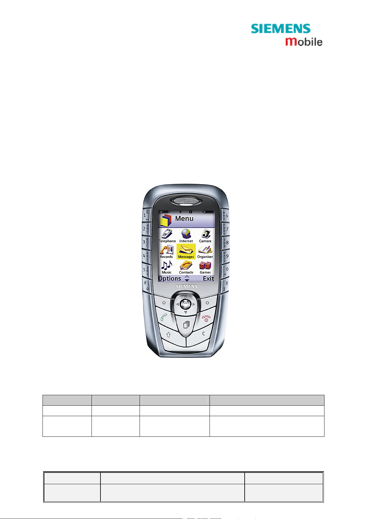
SX1
Company Confidential
Copyright 2003© Siemens AG
11/03
Page 2

Table of Contents:
1 LIST OF AVAILABLE LEVEL 2,5E PARTS SX1................................................ 5
2 REQUIRED EQUIPMENT FOR LEVEL 2,5E .................................................... 10
3 REQUIRED SOFTWARE FOR LEVEL 2,5E SX1 ............................................. 10
4 RADIO PART .................................................................................................... 11
4.1 Power Supply RF-Part .................................................................................. 12
4.2 Frequency generation .................................................................................. 12
4.2.1 Synthesizer: The discrete VCXO (26MHz).........................................................................12
4.2.2 Synthesizer: LO1................................................................................................................13
4.2.3 Synthesizer: LO2................................................................................................................16
4.2.4 Synthesizer: PLL ................................................................................................................17
4.3 Antenna switch (electrical/mechanical)...................................................... 18
4.4 Receiver......................................................................................................... 19
4.4.1 Receiver: EGSM900/GSM1800/GSM1900 –Filter to Demodulator...................................19
4.4.2 IC Overview........................................................................................................................21
4.5 Transmitter.................................................................................................... 22
4.5.1 Transmitter: Modulator and Up-conversion Loop...............................................................22
4.5.2 Transmitter: Power Amplifier..............................................................................................22
5 LOGIC ............................................................................................................... 23
5.1 Modem System ............................................................................................. 24
5.1.1 EGOLD+.............................................................................................................................24
5.1.2 SRAM.................................................................................................................................28
5.1.3 FLASH................................................................................................................................28
5.1.4 SIM .....................................................................................................................................28
5.1.5 Vibration Motor...................................................................................................................29
5.2 Power Supply ASIC Salzburg ...................................................................... 29
5.2.1 Pinout diagram ...................................................................................................................30
5.2.2 Power Supply Operating mode: .........................................................................................31
5.2.3 Power Supply Functions:....................................................................................................31
5.3 Battery ........................................................................................................... 33
5.4 Charging Concept......................................................................................... 34
5.5 Application system....................................................................................... 37
5.5.1 Application processor.........................................................................................................37
5.5.2 SDRAM...............................................................................................................................37
5.5.3 Flash...................................................................................................................................38
V 1.1 Page 2 of 63 ICM MP CCQ GRM T
SX1
Company Confidential
Copyright 2003© Siemens AG
11/03
Page 3

5.6 Power Supply ASIC Sofia............................................................................. 42
5.6.1 Pinout diagram ...................................................................................................................43
5.6.2 Power Supply Operating mode: .........................................................................................44
5.6.3 Regulator............................................................................................................................44
6 FM RADIO......................................................................................................... 46
7 BLUETOOTH ................................. FEHLER! TEXTMARKE NICHT DEFINIERT.
8 INTERFACES.................................................................................................... 48
8.1 Board to Board connector ........................................................................... 48
8.2 Vibra............................................................................................................... 50
8.3 Earpiece......................................................................................................... 51
8.4 Microphone ................................................................................................... 52
8.5 Battery ........................................................................................................... 52
8.6 IO Connector with ESD protection.............................................................. 53
8.6.1 IO Connector – New Slim Lumberg ...................................................................................53
8.6.2 ESD Protection with EMI filter............................................................................................54
8.7 SIM ................................................................................................................. 55
8.8 Display........................................................................................................... 55
9 ACOUSTIC........................................................................................................ 57
9.1 Microphone ................................................................................................... 57
9.1.1 Mechanical .........................................................................................................................57
9.1.2 Electrical.............................................................................................................................57
9.2 Soundchip ..................................................................................................... 58
9.3 Earpiece/Loudspeaker ................................................................................. 59
9.3.1 Mechanical .........................................................................................................................59
9.3.2 Electrical.............................................................................................................................59
10 DISPLAY AND ILLUMINATION..................................................................... 60
10.1 Display ........................................................................................................ 60
10.2 Illumination ................................................................................................ 60
11 KEYBOARD ................................................................................................... 61
12 BLUETOOTH (ONLY S55)............................................................................. 61
V 1.1 Page 3 of 63 ICM MP CCQ GRM T
SX1
Company Confidential
Copyright 2003© Siemens AG
11/03
Page 4

12.1 Bluetooth Voltage Regulator .................................................................... 62
13 IRDA ............................................................................................................... 63
V 1.1 Page 4 of 63 ICM MP CCQ GRM T
SX1
Company Confidential
Copyright 2003© Siemens AG
11/03
Page 5
1 List of available level 2,5e parts SX1
Main Board
ID-No Type Name, Location Part-No.
D800 IC Transceiver IC V20820-L6105-D670
D890 VCO Transmitter_VCO V20820-L6132-D670
D0950 IC Power Supply ASIC V30145-J4682-Y48
D1100 IC FEM Radio V20810-U6085-D670
D2300 IC Egold+ V39197-F5019-F415
D2700 IC Bluetooth_IC V39197-F5021-F381
C2803 Capacitor Cap. VDD_SIM V39377-F6105-K
C2811 Capacitor Cap. VCC2 8-VCCSYN V39344-F1225-K12
C2814 Capacitor Cap. VDD_CORE V39344-F1225-K12
C2815 Capacitor Cap. VDD_ANALOG-VDD_IO V39344-F1225-K12
C2816 Capacitor Cap. VDD_RTC V39392-F1107-M
N3225 IC Volt.Regulator_Camera V20810-C6065-D670
R959 Resistor Temp_Resistor V24852-C273-J2
V850 Transistor Tran._VCO_Switch
V1100 Diode Capa_Diode FEM V20840-D61-D670
V1101 Diode Capa_Diode FEM 1 V20840-D61-D670
V2182 Transistor Tran._Akku V20840-C4014-D670
V2501 Diode Diode_IO Connector V20840-D3084-D670
V2600 Transistor Tran._Vibra V20840-C4014-D670
V2601 Transistor Tran._Vibra 1 V24851-Z9112-Z998
V2700 Diode Diode_Bluetooth V20840-D73-D670
V2800 Transistor Tran._Charge V20830-C1107-D670
V2801 Transistor Tran._Power V20830-C1107-D670
V2802 Diode Diode_Power V20840-D3091-D670
Z850 VCO
Z851 Filter Filter_BALUN V30145-K260-Y41
Z880 IC Ant_Switch_Diplexer V30145-K280-Y244
Z900 IC Power_Amplifier V39197-F5005-F487
Z950 Quartz Oszillator_26MHz V39197-F5005-F33
Z2300 Quartz Quarz/Egold V30145-F102-Y10
Z2500 Filter Logic/IO_Interface V39197-F5000-F116
Z2700 Filter Filter_Bluetooth V30145-K280-Y256
1LO_VCO
V20820-C6047-D670
V30145-G100-Y105
V 1.1 Page 5 of 63 ICM MP CCQ GRM T
SX1
Company Confidential
Copyright 2003© Siemens AG
11/03
Page 6
MMI Board
ID-No Component ID Part-No.
R2002
R2003
R2001
R1100
R3004
R3011
R3019
R3020
R4004
R4009
R4011
R2011
R3000
R3009
R3012
R4000
R3015
R3016
R3017
R3018
R2010
R1005
R1006
R1007
R1008
R1009
R1010
R1011
R1012
R1013
R1014
R1015
R1016
R1017
R1018
R1019
R1020
R1021
R1022
R1023
R3002
R3014
R4002
R3003
R2002/R2003
R2002/R2003
R2001
Res_Type1
Res_Type1
Res_Type1
Res_Type1
Res_Type1
Res_Type1
Res_Type1
Res_Type1
R2011
R3000/R3009/R3012
R3000/R3009/R3012
R3000/R3009/R3012
R4000
Res_Type2
Res_Type2
Res_Type2
Res_Type2
R2010
Res_Type3
Res_Type3
Res_Type3
Res_Type3
Res_Type3
Res_Type3
Res_Type3
Res_Type3
Res_Type3
Res_Type3
Res_Type3
Res_Type3
Res_Type3
Res_Type3
Res_Type3
Res_Type3
Res_Type3
Res_Type3
Res_Type3
Res_Type3
Res_Type3
Res_Type3
Res_Type3
V24852-C -X
V24852-C -X
V39246-F4000-G
V24842-C -X
V24842-C -X
V24842-C -X
V24842-C -X
V24842-C -X
V24842-C -X
V24842-C -X
V24842-C -X
V24852-C10-J2
V24842-C100-J
V24842-C100-J
V24842-C100-J
V24842-C330-J
V24852-C560-J2
V24852-C560-J2
V24852-C560-J2
V24852-C560-J2
V24852-C680-J2
V24842-C101-J
V24842-C101-J
V24842-C101-J
V24842-C101-J
V24842-C101-J
V24842-C101-J
V24842-C101-J
V24842-C101-J
V24842-C101-J
V24842-C101-J
V24842-C101-J
V24842-C101-J
V24842-C101-J
V24842-C101-J
V24842-C101-J
V24842-C101-J
V24842-C101-J
V24842-C101-J
V24842-C101-J
V24842-C101-J
V24842-C101-J
V24842-C101-J
V24842-C101-J
V 1.1 Page 6 of 63 ICM MP CCQ GRM T
SX1
Company Confidential
Copyright 2003© Siemens AG
11/03
Page 7

R1002
R1003
R1024
R2013
R1201
R1202
R1203
R1204
R1205
R1206
R1207
R2009
R3010
R3005
R2006
R2007
R1000
R1004
R2005
R3013
R1200
R1212
R1001
R3001
R3008
R2000
R1208
R1209
R1210
R1211
R1222
R2008
R3007
C2014
C3000
C1200
C1201
C1202
C1203
C1204
C1205
C1206
C1207
C1208
C1209
C1210
C2017
C2006
R1002/R1003
R1002/R1003
R1024
R2013
Res_Type4
Res_Type4
Res_Type4
Res_Type4
Res_Type4
Res_Type4
Res_Type4
R2003
R3010
R3005
R2006/R2007
R2006/R2007
Res_Type5
Res_Type5
Res_Type5
Res_Type5
R1200/R1212
R1200/R1212
R1001/R3001/R3008
R1001/R3001/R3008
R1001/R3001/R3008
R2000
Res_Type6
Res_Type6
Res_Type6
Res_Type6
Res_Type6
R2008
R3007
C2014
C3000
Cap_Type1
Cap_Type1
Cap_Type1
Cap_Type1
Cap_Type1
Cap_Type1
Cap_Type1
Cap_Type1
Cap_Type1
Cap_Type1
Cap_Type1
Cap_Type1
C2006
V39246-F4121-G
V39246-F4121-G
V24842-C121-J
V24852-C331-J2
V24852-C681-J2
V24852-C681-J2
V24852-C681-J2
V24852-C681-J2
V24852-C681-J2
V24852-C681-J2
V24852-C681-J2
V24842-C102-J
V24842-C152-J
V24842-C472-J
V24842-C682-J
V24842-C682-J
V24842-C103-J
V24842-C103-J
V24842-C103-J
V24842-C103-J
V24852-C393-J2
V24852-C393-J2
V24842-C473-J
V24842-C473-J
V24842-C473-J
V24852-C104-F2
V24842-C224-J
V24842-C224-J
V24842-C224-J
V24842-C224-J
V24842-C224-J
V24842-C334-J
V39197-F5005-F975
V24843-C9060-D805
V24843-C9030-C305
V24843-C9180-J5
V24843-C9180-J5
V24843-C9180-J5
V24843-C9180-J5
V24843-C9180-J5
V24843-C9180-J5
V24843-C9180-J5
V24843-C9180-J5
V24843-C9180-J5
V24843-C9180-J5
V24843-C9180-J5
V24843-C9180-J5
V24843-C101-J5
V 1.1 Page 7 of 63 ICM MP CCQ GRM T
SX1
Company Confidential
Copyright 2003© Siemens AG
11/03
Page 8
C2024
C2025
C2016
C3018
C4004
C2001
C1000
C1001
C1002
C1003
C2000
C2002
C2005
C2007
C3001
C3002
C3006
C3007
C3008
C3009
C3010
C3011
C3012
C3013
C3014
C3015
C3016
C3017
C3021
C3022
C4000
C4001
C4002
C4003
C4005
C2003
C2004
C2008
C2019
C2018
C2012
C3024
C2009
C2010
C2011
C2015
C2020
C2021
C2024/C2025
C2024/C2025
C2016
C3018/C4004
C3018/C4004
C2001
Cap_Type2
Cap_Type2
Cap_Type2
Cap_Type2
Cap_Type2
Cap_Type2
Cap_Type2
Cap_Type2
Cap_Type2
Cap_Type2
Cap_Type2
Cap_Type2
Cap_Type2
Cap_Type2
Cap_Type2
Cap_Type2
Cap_Type2
Cap_Type2
Cap_Type2
Cap_Type2
Cap_Type2
Cap_Type2
Cap_Type2
Cap_Type2
Cap_Type2
Cap_Type2
Cap_Type2
Cap_Type2
Cap_Type2
Cap_Type3
Cap_Type3
Cap_Type3
Cap_Type3
C2018
C2012
C3024
Cap_Type4
Cap_Type4
Cap_Type4
Cap_Type4
Cap_Type5
Cap_Type5
V24853-C8121-G5
V24853-C8121-G5
V24853-C9102-K6
V24843-C102-K6
V24843-C102-K6
V24853-C9473-M4
V24853-C9104-M4
V24853-C9104-M4
V24853-C9104-M4
V24853-C9104-M4
V24853-C9104-M4
V24853-C9104-M4
V24853-C9104-M4
V24853-C9104-M4
V24853-C9104-M4
V24853-C9104-M4
V24853-C9104-M4
V24853-C9104-M4
V24853-C9104-M4
V24853-C9104-M4
V24853-C9104-M4
V24853-C9104-M4
V24853-C9104-M4
V24853-C9104-M4
V24853-C9104-M4
V24853-C9104-M4
V24853-C9104-M4
V24853-C9104-M4
V24853-C9104-M4
V24853-C9104-M4
V24853-C9104-M4
V24853-C9104-M4
V24853-C9104-M4
V24853-C9104-M4
V24853-C9104-M4
V24853-C6224-M6
V24853-C6224-M6
V24853-C6224-M6
V24853-C6224-M6
V39377-F4474-M
V39377-F6105-K
V24853-C6105-K6
V39377-F6225-M
V39377-F6225-M
V39377-F6225-M
V39377-F6225-M
V39375-F6106-M
V39375-F6106-M
V 1.1 Page 8 of 63 ICM MP CCQ GRM T
SX1
Company Confidential
Copyright 2003© Siemens AG
11/03
Page 9
C2023
C3005
C2022
C2013
L2001
L2002
V2000
V2003
V2001 V2001 V20840-D5035-D670
V1204 V1204 V20840-C4057-D670
V2002 V2002 V20830-C1121-D670
D4001 D4001 V30113-D1500-A2
D2002 D2002 V30145-J4682-Y44
D4000 D4000 V20810-F6232-D670
D3003
D3004
D3000
D1000
D3001
Z3001 Z3001 V39197-F5021-F966
Z3000 Z3000 V30145-G100-Y103
C3003
C3004
Cap_Type5
Cap_Type5
C2022
C2013
L2001/L2002
L2001/L2002
V2000/V2003
V2000/V2003
D3003/D3004
D3003/D3004
D3000
D1000/D3001
D1000/D3001
C3003/C3004
C3003/C3004
V39375-F6106-M
V39375-F6106-M
V39391-F1336-M
V39344-F1225-K12
V39151-F5103-M8
V39151-F5103-M8
V20840-D5078-D670
V20840-D5078-D670
V20810-B6129-D670
V20810-B6129-D670
V39197-F5003-F786
V20810-B6079-D670
V20810-B6079-D670
V24843-C9150-J5
V24843-C9150-J5
V 1.1 Page 9 of 63 ICM MP CCQ GRM T
SX1
Company Confidential
Copyright 2003© Siemens AG
11/03
Page 10

2 Required Equipment for Level 2,5e
- GSM-Tester (CMU200 or 4400S incl. Options)
- PC-incl. Monitor, Keyboard and Mouse
- Bootadapter 2000/2002 (L36880-N9241-A200)
- Adapter cable for Bootadapter due to new Lumberg connector
- Troubleshooting Frame SX1 (F30032-P297-A1) MMI (F30032-P351)
- Power Supply
- Spectrum Analyser min. 4GHz
- Active RF-Probe incl. Power Supply
- Oscilloscope incl. Probe
- RF-Connector (N<>SMA(f))
- Power Supply Cables
- Dongle (F30032-P28-A1) if USB-Dongle is used a special driver for NT is required
- BGA Soldering equipment
Reference: Equipment recommendation V1.2
(downloadable from the technical support page)
3 Required Software for Level 2,5e SX1
- Windows NT Version4 or Win2000
- Winsui version1.43 or higher (OMAP for MMI)
- Software for GSM-Tester ( Cats(Acterna/Wiltek) or CMU-GO(Rohde&Schwarz) )
- Software for reference oscillator adjustment
- Internet unblocking solution
- Dongle driver for USB-Dongle if used with WIN NT4
V 1.1 Page 10 of 63 ICM MP CCQ GRM T
SX1
Company Confidential
Copyright 2003© Siemens AG
11/03
Page 11

4 Radio Part
The radio part of the SX1, is using a Hitachi
The radio part is designed for Tripple Band operation, covering EGSM900, GSM1800 as well as GSM
1900 frequencies, and can be divided into 4 Blocks.
-Power supply for RF-Part
-Transmitter
-Receiver
-Synthesizer,
The RF-Part has it´s own power supply realised by a voltage regulator which is located
inside the ASIC. The voltages for the logic part are generated by the Power-Supply ASIC too.
The transmitter part converts the I/Q base band signals supplied by the logic (EGOLD+) into RF-
signals with characteristics as defined in the GSM recommendation (
by a power Amplifier the signal is radiated via the internal or external antenna.
The receiver part converts the received GMSK signal supplied by the antenna into IQ base band
signals which are further processed by the logic (EGOLD+).
The synthesizer generates the required frequencies for the transmitter and receiver. A 26MHz
oscillator is acting as a reference frequency.
Restrictions:
The mobile phone can never transmit and receive in both bands simultaneously. Only the monitor time
slot can be selected independently of the frequency band. Transmitter and receiver can of course
never operated simultaneously.
www.etsi.org) After amplification
V 1.1 Page 11 of 63 ICM MP CCQ GRM T
SX1
Company Confidential
Copyright 2003© Siemens AG
11/03
Page 12
V
VCC_
4.1 Power Supply RF-Part
The voltage regulator for the RF-part is located inside the ASIC D2802. It generates the required 2,8V
“RF-Voltages” named VCC2_8 and VCC_SYN . The voltage regulator is activated as well as
deactivated via M_RF1_EN
EGOLD+. The temporary deactivation is used to extend the stand by time.
Circuit diagram
(TDMA-Timer H16) and VCXOEN_UC (Miscellaneous R6) provided by the
CC2_8
SYN
4.2 Frequency generation
4.2.1 Synthesizer: The discrete VCXO (26MHz)
The SX1 mobile is using a reference frequency of 26MHz for the Hitachi chip set. The generation of
the 26MHz signal is done via a TVCXO Z950. TP (test point) of the 26MHz signal is the TP 2310
The oscillator output signal 26MHz_RF is directly connected to the BRIGHT IC (pin 38) to be used as
reference frequency inside the Bright (PLL). The signal leaves the Bright IC as BB_SIN26M at (pin 36)
to be further used from
the EGOLD+ (D100
Bright 4
To compensate frequency drifts (e.g. caused by temperature) the oscillator frequency is controlled by
the (AFC) signal, generated through the internal EGOLD+ (D100
diode V951. Reference for the “EGOLD-PLL” is the base station frequency. To compensate a
temperature caused frequency drift, the temperature-depending resistor R959 is placed near the
VCXO to measure the temperature. The measurement result TVCXO is reported to the
EGOLD+
The required voltage VCC_SYN is provided by the ASCI D2820
(Analog Interface P3) via R138 as the signal TENV.
(functional T3)).
(functional U5)) PLL via the capacity
V 1.1 Page 12 of 63 ICM MP CCQ GRM T
SX1
Company Confidential
Copyright 2003© Siemens AG
11/03
Page 13
Circuit diagram
from EGOLD
to Bright IC
to Bluetooth IC
4.2.2 Synthesizer: LO1
The first local oscillator is needed to generate frequencies which enables the transceiver IC to
demodulate the receiver signal and to perform the channel selection in the TX part. To do so, a control
voltage for the LO1 is used. Gained by a comparator. (located inside the Transceiver (Bright -IC)).
This control voltage is a result of the comparison of the divided LO1 and the 26MHz reference Signal.
The division ratio of the dividers is programmed by the EGOLD+, according to the network channel
requirements.
The first local oscillator (LO1) consists of the PLL inside the Bright (D800), an external loop filter and
the VCO (Z850) module. LO1 generates frequencies from:
3700-3980 MHz for EGSM900
3580-3760 MHz for GSM1800
3860-3980 MHz for GSM1900
Formula for TX frequencies:
EGSM900
Channel: 975...1023/76...92 = (Ch. freq. + 82MHz) * 4
Channel: 0…75/93…124 = (Ch. freq. + 80MHz) * 4
GSM1800
Channel: 512...661 = (Ch. freq. + 80MHz) * 2
Channel: 662…885 = (Ch. freq. + 82MHz) * 2
GSM1900
Channel: 512...810 = (Ch. freq. + 80MHz) * 2
26MHz
Formula for RX frequencies:
EGSM900
Channel freq. * 4
GSM1800
Channel freq. * 2
GSM1900
Channel freq. * 2
V 1.1 Page 13 of 63 ICM MP CCQ GRM T
SX1
Company Confidential
Copyright 2003© Siemens AG
11/03
Page 14
The VCO (Z850) is switched on by the EGOLD+ signal PLLON (TDMA-Timer F16) via V850 and therefore
supplied with VCC2_8. The VCO guarantees by using the control voltage at pin5 a coverage of the
EGSM900, GSM1800 and GSM1900 frequency band and frequency stability. The Bright gained
control voltage passes on the way to the VCO a discreet loop filter (typical value from 0,5 – 2,1V).
The channel programming of the PLL happens via the EGOLD+ signals RFDATA; RFCLK; RFSTR.
(RF Control J15, J16, J17). If the Bright IC gets via the same signals a GSM1800 channel information, the
VCO is switched to this frequency by Pin 42 Bright (Pin 3 VCO).
For GSM900 - RX = “low signal” for channel 975-49
= “high signal” for channel 50-124
- TX = “high signal” for all channels
For GSM1800 - RX = “low signal” for all channels
- TX = “low signal” for all channels
For GSM1900 - RX = “high signal” for all channels
- TX = “high signal” for all channels
The VCO output signal passes the “Balun” transformer (Z851) with insertion losses of ~ 2dB to arrive
at the Bright IC.
The required voltage VCC8_8 is provided by the ASIC D2820
Circuit diagram
from EGOLD+
Balun transformer
Bright 4
26MHz
V 1.1 Page 14 of 63 ICM MP CCQ GRM T
SX1
Company Confidential
Copyright 2003© Siemens AG
11/03
Page 15

V 1.1 Page 15 of 63 ICM MP CCQ GRM T
SX1
Company Confidential
Copyright 2003© Siemens AG
11/03
Page 16
VCO
TOP
View
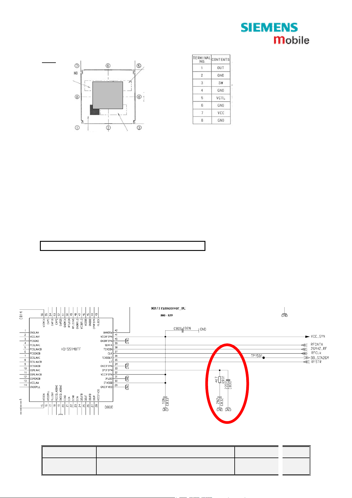
4.2.3 Synthesizer: LO2
The second local oscillator is required for transmitter operations only. It consists of a PLL and a VCO
which are integrated inside the Bright 4, and an external second order loopfilter (R831; C830; C832).
Before the VCO generated 640 or 656MHz signal arrives at the modulator, it is divided by 8. So the
resulting frequency after the IQ modulator is 80/82MHz (depending on channel and band).
Programming of the LO2 PLL is done in the same way as described at the LO1. The tree-wire-bus
(EGOLD+ signals RFDATA; RFCLK; RFSTR.
stability, the 640MHz VCO signal is compared by the phase detector of the 2
reference signal. The resulting control signal passes the external loop filter and is used to control the
640/656MHz VCO.
The required voltage VCC_SYN is provided by the ASIC D2820
Circuit diagram
(RF Control J15, J16, J17) is used. To ensure the frequency
nd
PLL with the 26MHz
Loop-filter LO2
V 1.1 Page 16 of 63 ICM MP CCQ GRM T
SX1
Company Confidential
Copyright 2003© Siemens AG
11/03
Page 17
4.2.4 Synthesizer: PLL
PLL as a part of the BRIGHT IC
Blockdiagram
V 1.1 Page 17 of 63 ICM MP CCQ GRM T
SX1
Company Confidential
Copyright 2003© Siemens AG
11/03
Page 18
p
r
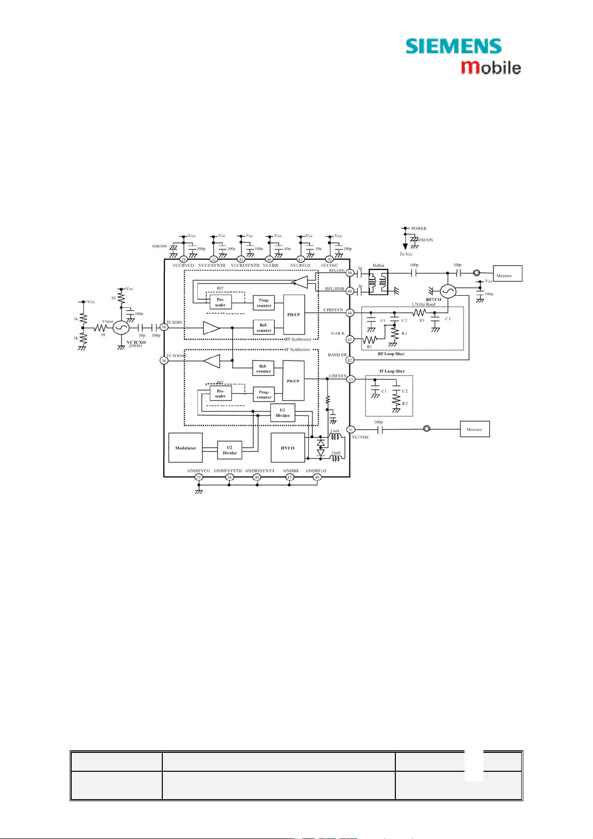
4.3 Antenna switch (electrical/mechanical)
Internal/External <> EGSM900/GSM1800/GSM1900 <> Receiver/Transmitter
The SX1 mobile has two antenna switches.
a) The mechanical antenna switch for the differentiation between the internal and external
antenna
b) The electrical antenna switch, for the differentiation between the receiving and transmitting
signals. To activate the correct settings of this diplexer, the EGOLD+ signals RF_SW and
TXON_GSM are required
Circuit diagrams
a) Internal/External antenna switch
to / from
lexe
di
b) The electrical antenna switch
External
Antenna
Internal
Antenna
to Antenna
to
Bright
V 1.1 Page 18 of 63 ICM MP CCQ GRM T
SX1
Company Confidential
Copyright 2003© Siemens AG
11/03
Page 19
Z880
Top View
4.4 Receiver
4.4.1 Receiver: EGSM900/GSM1800/GSM1900 –Filter to Demodulator
From the antenna switch, up to the demodulator the received signal passes the following blocks to get
the demodulated baseband signals for the EGOLD+:
Filter
LNA
Z880 Bright
Filter: The EGSM900, GSM1800 and GSM 1900 filters are located inside the frontend module. The
Filter are centred to a frequency of 942,5MHz for EGSM900, 1847,5MHz for GSM1800 and 1960MHZ
for GSM1900. The symmetrical filter output is matched via LC-Combinations to the LNA input of the
BRIGHT (D800)
LNA: The 2 LNA´s (EGSM900/GSM1800/GSM1900) are located inside the BRIGHT and are able to
perform an amplification of ~ 20dB. The LNA can be switched in HIGH (On) and LOW (Off) mode and
is controlled by the Bright depending on EGOLD+ information.
Demodulator: The Bright IC performs a direct demodulation of the received GSM signals. To do so the
LO1 is required. The channel depending LO1 frequencies for 1800MHz/1900MHz bands are divided
by 2 and by 4 for 900MHz band, Bright internally.
PGC: After demodulation the “I” and “Q” signals are amplified by the PGC-Amplifier the “I” and the “Q”
path are amplified independently from each other. The performance of this PGC is 80dB (-26 up to
54dB), switchable in steps of 2dB. The control is realised through the EGOLD+ signals (RFDATA;
RFCLK; RFSTR.
the double using of RX and TX lines), the signals are ready for further processing through the EGAIM
(part of the EGOLD+) The post-switched logic measures the level of the demodulated baseband
signal an regulates the level to a defined value by varying the PGA-Amplification and switching the
appropriate LNA gains
The required voltage VCC_SYN is provided by the ASIC D2820
(RF Control J15, J16, J17). After passing a Bright internal switch (necessary because of
Demodulator
PGC
V 1.1 Page 19 of 63 ICM MP CCQ GRM T
SX1
Company Confidential
Copyright 2003© Siemens AG
11/03
Page 20

Circuit diagram
from LO1
from
antenna
progr. signals
to EGOLD+
V 1.1 Page 20 of 63 ICM MP CCQ GRM T
SX1
Company Confidential
Copyright 2003© Siemens AG
11/03
Page 21

4.4.2 IC Overview
IC Overview
BRIGHT IV
V 1.1 Page 21 of 63 ICM MP CCQ GRM T
SX1
Company Confidential
Copyright 2003© Siemens AG
11/03
Page 22

4.5 Transmitter
4.5.1 Transmitter: Modulator and Up-conversion Loop
The modulation is based on the principle of the “up-conversion modulation phase locked loop” and is
accomplished via the BRIGHT IC(D800). An internal TX IF-LO provides the quadratic modulator with
the TX IF frequency of 80/82 MHz by generating 640/656MHz divided by 8. This so generated IF
GMSK RF signal is compared in a phase detector with the down mixed GMSK RF output from the TXVCO (Z150). To get the comparison signal, PCN_PA_IN (for GSM1800/GSM1900), and GSM_PA_IN
(for EGSM900) appearing at Pin 9/7 of the (D150) are mixed with the LO1 signal (divided by 2 for
GSM1800/GSM1900 and 4 for EGSM900). The output (PLLOUT) signal of the phase detector passes
a discrete loop filter realised by capacitors and resistors to set the TXVCO to required frequency. The
large loop band width (~1,5MHz) guarantees that the regulating process is considerably quicker than
the changes in the modulation signal.
The required voltage VCC_SYN and VCC2_8 is provided by the ASIC D2820
4.5.2 Transmitter: Power Amplifier
The output signals (CS_PA_IN , and GSM_PA_IN) from the limited amplifier are led to the power
amplifier (Z600) passing a matching circuit. contains two separate 3-stage amplifier chains for GSM
850/900 and GSM 1800/1900. The control of the output power is handled via one Vapc port. The
power control circuit itself is integrated in the PA module. The EGOLD generates the power control
signal PA-RAMP. The band selection switching is done via OSW1 from the Smarti IC.
The required voltage BATT+ is provided by the battery.
The required voltage VREGRF2 for the power control circuit is provided by the ASIC D2820.
from BRIGHT
to FEM
V 1.1 Page 22 of 63 ICM MP CCQ GRM T
SX1
Company Confidential
Copyright 2003© Siemens AG
11/03
Page 23

5 Logic
V 1.1 Page 23 of 63 ICM MP CCQ GRM T
SX1
Company Confidential
Copyright 2003© Siemens AG
11/03
Page 24

5.1 Modem System
5.1.1 EGOLD+
Block Diagram EGOLD+ V3.1
8
8 16
21 24
Osc.
32.768 kHz
16
Debug Support
CS(4:0)
3
Pulse-Carry Mod.
CAPCOM
2 x 8 bit
ID Register
6
Multicore
External
Bus & Port
Controller
AFC Unit
RTC
5
compatible
32 kHz
PD-Bus
SSC
3
SPI
MMCI
V5.4
ASC0
Autobaud
Detect
GPT1/GPT2
Watchdog
80
SRAM
256k x 8
I2C
2
2
ASC1
13/26/52 MHz / 32 kHz
READY#
NMI#
HOLD#
HLDA#
CLKOUT
RSTOUT#
OCDS DPEC
Interrupt Controller
Clock Generation
Peripheral Enable
Generator
Power
Management
MCU
C166S
Dual Port RAM
1k x 16
LM-Bus
PROM
1k x 16
Boot
Enable Signals to
X- and PD-Bus Peripherals
78 MHz
X-Bus
OCEM
Block
16 bit I/O Ports
I2S
DSP Timer1
OAK78 DSP
x
Interleaving / De-Interleaving
x
Speech Coding/Decoding
x
Level Measurement
x
Channel Coding/Decoding
x
Equalization
x
Encryption / Decryption
x
Voice Memo/Voice Dialing
x
GPRS support
Interrupt Controller
SEIB
Interface
3
DSP Serial
Comm. Interface /
DAI
DSP Timer2
(FR, HR, EFR, AMR)
(FR, HR, EFR, AMR)
Bus
Unit
6
Shared Memory
Dual Port 512 x 16
Accelerator
Cipher Unit
2
SIM card
Interface
High Speed
(F=512, D=8/16)
GPRS
Cipher Unit
Logic
Arranger
(LPA)
GSM
TDMA Timer
8 3
4
RF Control
Keypad
Interface
4
6
The EGOLD+ contains a 16-bit micro-controller (µC part), a GSM analog Interface (EGAIM), a DSP computing core (DSP part) and an interface for application-specific switch-functions.
The µC part consists of the following:
• Micro-controller
• System interfaces for internal and external peripheries
• On-chip peripheries and memory
The Controller Firmware carries out the following functions:
• Control of the Man Machine Interface (keypad, LCD, sensing element, control of the illumination,...)
• GSM Layer 1,2,3 /GPRS
• Control of radio part (synthesizer, AGC, AFC, Transmitter, Receiver...),
• Control of base band processing (EGAIM)
• Central operating system functions (general functions, chip select logic, HW driver, control of
mobile phones and accessories...).
E-GOLD+ V3.0 Architecture
Single Chip Cellular Baseband Processor
Package: P-LFBGA-208
Viterbi
HW
A51/52
P ROM
60k x 16
P RAM
4k x 16
Y RAM
2k x 16
X RAM
15k x 16
X ROM
36k x 16
GMSK
Modulator
Voiceband
Filters
RX and TX
Baseband
Filter/
Cordic-
Processor
TAP Controller
JTAG
Boundary Scan
Interp./
Noise
Shaper
Interp./
Noise
Shaper
Σ∆
ADC
Σ∆
DAC
Σ∆
ADC
12 bit resolution
Σ∆
ADC
Switch Matrix
Battery & Temperature
Measurement
RF Output
Power Control
10 bit DAC
reference
voltage
confidential
DAC
R-String
DAC
R-String
MUX
Bandgap
2
2
2
2
2
2
2
2
V 1.1 Page 24 of 63 ICM MP CCQ GRM T
SX1
Company Confidential
Copyright 2003© Siemens AG
11/03
Page 25

The EGAIM part contains the interface between the digital and the analogue signal processing:
• 2 Sigma Delta A/D converters for RX signal, and for the necessary signals for the charge control
and temperature measurement. For this, the converter inputs are switched over to the various
signals via the multiplexer.
• 2 D/A converters for the GMSK-modulated TX signal,
• 1 D/A converter for the Power Ramping Signal,
• 1 Sigma Delta A/D and D/A converter for the linguistic signal.
Blockdiagram EGAIM inside the EGOLD
V 1.1 Page 25 of 63 ICM MP CCQ GRM T
SX1
Company Confidential
Copyright 2003© Siemens AG
11/03
Page 26

Measurement of Battery and Ambient Temperature
The battery temperature is measured via the voltage divider R1387, R138 by the EGOLD+
Interface P2).
For this, the integrated Σ∆ converter of the RX-I base band branch is used. This Σ∆
(Analog
converter compares the voltage of TBAT and TENV internally. Through an analogue multiplexer,
either the RX-I base band signal, or the TBAT signal and the TENV signal is switched to the input of
the converter. The signal MEAS_ON from the EGOLD+
(GSM TDMA-TIMER H15) activates the battery
voltage measurement The ambient temperature TENV is measured directly at of the EGOLD+
(Analog Interface P3).
Measurement of the Battery Voltage
The measurement of the battery voltage is done in the Q-branch of the EGOLD+, for this BATT+ is
connected via a voltage divider R143, R146 to the EGOLD+
multiplexer does the switching between the baseband signal processing and the voltage
measurement.
(Analog Interface P1). An analogue
V 1.1 Page 26 of 63 ICM MP CCQ GRM T
SX1
Company Confidential
Copyright 2003© Siemens AG
11/03
Page 27

A/D conversion of MIC-Path signals incl. coding
The Microphone signals (MICN2, MIP2, MICP1, MICN1) arrive at the voiceband part of the EGOLG+.
For further operations the signals will be converted into digital information, filtered, coded and finally
formed into the GMSK-Signal by the internal GMSK-Modulator. This so generated signals (RF_I,
RF_IX, RF_Q, RF_QX) are given to the Bright IC in the transmitter path.
D/A conversion of EP-Path signals incl. decoding
Arriving at the baseband-Part the demodulated signals (RF_I, RF_IX, RF_Q, RF_QX) will be filtered
and A/D converted. In the voiceband part after decoding (with help of the µC part) and filtering the
signals will be D/A converted amplified and given as (EPP1_FIL, EPN1_FIL) to the Power Supply
ASIC.
Generation of the PA Control Signal (PA_RAMP)
The RF output power amplifier needs an analogue ramp up/down control voltage. For this the system
interface on EGOLD+ generates 10 bit digital values which have to be transferred serially to the power
ramping path. After loading into an 10 bit latch the control value will be converted into the
corresponding analogue voltage with a maximum of ~2V
-
V 1.1 Page 27 of 63 ICM MP CCQ GRM T
SX1
Company Confidential
Copyright 2003© Siemens AG
11/03
Page 28

The DSP part contains:
• DSP signal processor
• Separate program/data memory
• a hardware block for processing the RX signal,
• a hardware block for “ciphers“,
• a hardware block for processing the linguistic signal,
• a hardware block for the “GMSK modulator“,
• De-/ interleaving memory,
• Communication memory
• a PLL for processing and reproducing the VCXO pulse signal.
In the DSP Firmware are implemented the following functions:
• scanning of channels, i.e., measurement of the field strengths of neighbouring base stations
• detection and evaluation of Frequency Correction Bursts
• equalisation of Normal Bursts and Synchronisation Bursts
• channel encoding and soft-decision decoding for fullrate, enhanced-fullrate and
adaptive multirate speech, fullrate and halfrate data and control channels.
• channel encoding for GPRS coding
• fullrate, enhanced fullrate and adaptive multirate speech encoding and decoding
• mandatory sub-functions like
– discontinuous transmission, DTX
– voice activity detection
– background noise calculation
• generation of tone and side tone
• hands-free functions
• support for voice memo
• support for voice dialling
• loop-back to GSM functions
• GSM Transparent Data Services and Transparent Fax
• calculation of the Frame Check Sequence for a RLP frame used for GSM NonTransparent Data
Services
• support of the GSM ciphering algorithm
Real Time Clock (integrated in the EGOLD+):
The real time clock is powered via a separate voltage regulator inside the Power Supply ASIC. Via a
capacitor, data are kept in the internal RAM during a battery change for at least 30 seconds. An alarm
function is also integrated with which it is possible to switch the phone on and off.
5.1.2 SRAM
Memory for volatile data
Memory Size: 4 Mbit
Data Bus: 16Bit
5.1.3 FLASH
Memory Size: 64Mbit (8 Mbyte)
Data Bus: 16 Bit
5.1.4 SIM
SIM cards with supply voltages of 1.8V and 3V are supported.
V 1.1 Page 28 of 63 ICM MP CCQ GRM T
SX1
Company Confidential
Copyright 2003© Siemens AG
11/03
Page 29

5.1.5 Vibration Motor
The vibration motor is mounted in the lower case. The electrical connection to the PCB is realised with
pressure contacts.
5.2 Power Supply ASIC Salzburg
The power supply ASIC contains the following functions:
• Powerdown-Mode
• Sleep Mode
• Trickle Charge Mode
• Power on Reset
• Digital state machine to control switch on and supervise the µC with a watchdog
• Voltage regulator
• Low power voltage regulator
• Additional output ports
• Voltage supervision
• Temperature supervision with external and internal sensor
• Battery charge control
• TWI interface
2C interface
• I
• RC Oscillator
• Audio multiplexer
• Audio amplifier stereo/mono
• 18 bit Sigma/Delta DAC with Clock recovery
• Bandgap reference*
INFO:
* Bandgap reference
The p-n junction of a semiconductor has a bandgap-voltage. This bandgap-voltage is almost
independent of changes in the supply voltage and has a very low temperature gradient. The bandgapvoltage is used as reference for the voltage regulators.
To reduce the power dissipation of the ASIC and to ensure high efficiency of the power management
concept a DCDC Converter for the Core (EGOLD+V3 Baseband Chipset), Flash and SRAM supply is
used.
The DCDC converter includes the following functions:
• PFM Mode for sleep mode of the Mobile Phone.
• PWM Mode for active mode of the Mobile Phone.
The mode change is controlled by the ASIC with the signal EN_DC_DOWN based on the EGOLD+
signal VCXO_EN.
V 1.1 Page 29 of 63 ICM MP CCQ GRM T
SX1
Company Confidential
Copyright 2003© Siemens AG
11/03
Page 30

5.2.1 Pinout diagram
V 1.1 Page 30 of 63 ICM MP CCQ GRM T
SX1
Company Confidential
Copyright 2003© Siemens AG
11/03
Page 31

5.2.2 Power Supply Operating mode:
- Power Down Mode (mobile is switched off)
In power down mode the current consumption is very low. The inputs for switch on conditions
(ON/OFF PinH2, ON/OFF2 PinJ3, VDD_CHARGE PinC3), the LPREG with his own voltage reference
and POR cells are active. All other blocks are switched off, so the battery discharging will be kept to a
minimum. This is the state when the phone is switched off.
- Start Up Mode (user switch on, RTC switch on)
“Start Up Mode” can be initiated by ON_OFF (falling edge) or ON_OFF2 (rising edge). In this mode a
sequential start-up, of reference oscillator, voltage supervision and regulators is controlled by digital
part. In case of failure (overvoltage or time out of the µC reaction), the ASIC shuts down.
-Trickle Charge Mode (to be able to charge the battery)
In case of a rising edge at VDD_CHARGE, the ASIC goes from power down to an interim state. In this
state, the oscillator and the reference are started. If the voltage on VDD_CHARGE is below the
charger detection threshold, the ASIC shuts off. If the voltage on VDD_CHARGE is high enough the
signal EXT_PWR is going to H and the power up continues . Depending on the voltage of the battery
an initial charging of the battery of the circuit is immediately done. If the Trickle Charge Mode is
entered with a very low battery, the supply for the ASIC itself is generated from the internal VDDREF
regulator. If a failure is detected (overvoltage), the ASIC is switched off.
- Normal Mode (following Start Up Mode or Trickle Charge Mode)
The normal mode is the situation, where the startup has been finished and the ASIC starts the
external µC by changing the signal RESETN from low to high.
Mode: a) Active Mode with full capabilities of all blocks
b) Sleep Mode with reduced capabilities of some blocks and some even not
available at all.
-Active Mode (submode of Normal Mode)
In this mode, the µC controls the charging block and most of the failure cases. The ASIC can be
controlled by the TWI interface, interrupt request can be sent by the ASIC. Furthermore, the voltages
are supervised ( in case of failure the µC will be informed). In case of watchdog failure, overvoltage or
power on request, the ASIC will be switched off immediately. The mono and the stereo block can be
switched on in active mode.
-Sleep Mode (submode of Normal Mode)
Intention of the mode is to have a limited set of functions available with a reduced current
consumption. A low level at the pin SLEEP1_N will switch from Active Mode to Sleep Mode. In Sleep
Mode all charging functions and supply overvoltage detection are switched off. LDO undervoltage
detection, clock and reference voltages are active. LDOs are working in low current mode. The battery
voltage comparators are available, the audio block can be switched on.
5.2.3 Power Supply Functions:
- Power on Reset
To guarantee a defined startup, the ASIC will be reset by a Power on Reset block. After Power on
Reset the ASIC will enter the power done Mode. If the thresholds will be reached during operating
mode the reset will become the device enters the power down mode. This blocks are always active
and will be supplied by VDDREF.
V 1.1 Page 31 of 63 ICM MP CCQ GRM T
SX1
Company Confidential
Copyright 2003© Siemens AG
11/03
Page 32

- Switch on and watchdog
There are 3 different possibilities to switch on the phone via external pins:
-VDD_CHARGE with rising edge
-ON/OFF with falling edge
-ON/OFF2 with rising edge
In order to guarantee a defined start-up behavior of the external components, a sequential power up is
used and the correct start up of blocks is supervised. In normal mode, a continues watchdog signal
from the µC is needed to keep the system running. If this signals fails, the ASIC will switch to power
down mode.
It must be guaranteed, that each start up condition does not interfere and block the other possible
start up signals. In case of failure during start up, the device will go back to power down mode. To
guarantee that the connection of the a charging unit with a very low battery is detected, this detection
must work level sensitive at the end of POR signal.
V 1.1 Page 32 of 63 ICM MP CCQ GRM T
SX1
Company Confidential
Copyright 2003© Siemens AG
11/03
Page 33

- Watchdog monitoring
As soon as the first Watchdog_µC pin rising is detected , the device start the watchdog monitoring
procedure. Standard switch off of the phone is the watchdog. The first edge of watchdog is rising. If a
falling edge is detected ass the first transient the device will go to power down mode again and the
whole phone is switched off.
Rising and falling edges must be detected alternated. With any edge on Watchdog_µC pin a counter
will be loaded. The next – compared to the previous edge – inverted edge must occur between end of
TA0,TA1 and end of TB0,TB1. If the signal occurs before end of TA0, TA1 or is not detected until end
of TB0, TB1, the device will go to power down mode immediately after the violation of the WD criteria
occurs.
TA0, TA1 ~ 0.4 sec
TB0, TB1 ~ 3 sec
5.3 Battery
As battery a LiIon battery with a nominal capacity of 3,7 Volt/1000mAh is used. Inside the battery
package a IC is placed to ensure that only original batteries are used. The logic of the battery is
connected via a one line RX/TX bus (BAT_RX_TX) with the Application Processor OMAP.
V 1.1 Page 33 of 63 ICM MP CCQ GRM T
SX1
Company Confidential
Copyright 2003© Siemens AG
11/03
Page 34

5.4 Charging Concept
Charging current
Charging control signal
5.4.1.1 Charging Concept
General
The battery is charged in the unit itself. The hardware and software is designed for LiIon with 4.2V
technology.
Charging is started as soon as the phone is connected to an external charger. If the phone is not
switched on, then charging takes place in the background (the customer can see this via the “Charge”
symbol in the display). During normal use the phone is being charged (restrictions: see below).
Charging is enabled via a PMOS switch in the phone. This PMOS switch closes the circuit for the
external charger to the battery. The EGOLD+ takes over the control of this switch depending on the
charge level of the battery, whereby a disable function in the POWER SUPPLY ASIC hardware can
override/interrupt the charging in the case of over voltage of the battery (only for Manganese
Chemistry Battery types e.g. NEC).
With the new slim Lumberg IO connector we lose the charger recognition via SB line. Now we
measure the charge current inside the POWER SUPPLY ASIC with a current monitor.
The charging software is able to charge the battery with an input current within the range of 350600mA. If the Charge-FET is switched off, then no charging current will flow into the battery (exception
is trickle charging, see below).
For controlling the charging process it is necessary to measure the ambient (phone) temperature and
the battery voltage. The temperature sensor will be an NTC resistor with a nominal resistance of 22kΩ
at 25°C. The determination of the temperature is achieved via a voltage measurement on a voltage
divider in which one component is the NTC. The NTC for the ambient temperature will be on the PCB
(26 MHz part).
V 1.1 Page 34 of 63 ICM MP CCQ GRM T
SX1
Company Confidential
Copyright 2003© Siemens AG
11/03
Page 35

Measurement of Battery, Battery Type and Ambient Temperature
The voltage equivalent of the temperature and battery code on the voltage separator will be calculated
as the difference against a reference voltage of the EGOLD. For this, the integrated Σ∆ converter in
the EGOLD of the RX-I base band branch will be used. Via an analogue multiplexer, either the RX-I
base band signal, the battery code voltage or the ambient temperature voltage can be switched over
to the input of the converter. The 1-Bit data stream of the converter will be subjected to a data
reduction via the DSP circuit so that the measured voltage (for battery and ambient temperature) will
be available at the end as a 10-bit data word.
Measurement of the Battery Voltage
Analogue to the I-branch either the RX-Q base band signal or the battery voltage can be measured in
the Q-branch. Processing in the DSP circuit will be done analogue to the I-branch. The EGOLD will be
specified internally at voltage measurement input BATT+ for an input voltage of 3V...4.5V.
Timing of the Battery Voltage Measurement
Unless the battery is charging, the measurement is made in the TX time slot. During charging it will be
done after the TX time slot. At the same time, either the battery temperature (in the I-branch) and the
battery voltage (in the Q-branch) or the ambient temperature in the I-branch can be measured (the
possibility of measurement in the Q-branch, the analogue evaluation of the battery coding, is used for
HW-Coding). Other combinations are not possible. For the time of the measurement the multiplexer in
the EGAIM must be programmed to the corresponding measurement.
Recognition of the Battery Type
The battery code is a resistor with a resistance depending on the manufacturer.
Charging Characteristic of Lithium-Ion Cells
LiIon batteries are charged with a U/I characteristic, i.e. the charging current is regulated in relation to
the battery voltage until a minimal charging current has been achieved. The maximum charging
current is approx. 600mA, minimum about 100mA. The battery voltage may not exceed 4.2V ±50mV
average. During the charging pulse current the voltage may reach 4.3V. The temperature range in
which charging of the phone may be started ranges from 5...40°C, and the temperature at which
charging takes place is from 0...45°C. Outside this range no charging takes place, the battery only
supplies current.
V 1.1 Page 35 of 63 ICM MP CCQ GRM T
SX1
Company Confidential
Copyright 2003© Siemens AG
11/03
Page 36

Trickle Charging
The POWER SUPPLY ASIC is able to charge the battery at voltages below 3.2V without any support
from the charge SW. The current will by measured indirectly via the voltage drop over a shunt resistor
and linearly regulated inside the POWER SUPPLY ASIC. The current level during trickle charge for
voltages <2.8V is in a range of 20-50mA and in a range of 50-100mA for voltages up to 3.75V. To limit
the power dissipation of the dual charge FET the trickle charging is stopped in case the output voltage
of the charger exceeds 10 Volt. The maximum trickle time is limited to 1 hour. As soon as the battery
voltage reaches 3.2 V the POWER SUPPLY ASIC will switch on the phone automatically and normal
charging will be initiated by software (note the restrictions on this item as stated below).
Normal Charging
For battery voltages above 3.2 Volt and normal ambient temperature between 5 and 40°C the battery
can be charged with a charge current up to 1C*. This charging mode is SW controlled and starts if an
accessory (charger) is detected with a supply voltage above 6.4 Volt by the POWER SUPPLY ASIC.
The level of charge current is limited/controlled by the accessory or charger.
USB Charging
For battery voltages above 3.2 Volt and normal Temperature between 5 and 40°C the battery can be
charged with a charge current up to 1C. This charging mode is SW controlled and starts if an
accessory (charger) with a supply voltage between 3.6 and 5.4 Volt is detected by the POWER
SUPPLY ASIC during active mode of the phone. To enable this charging mode, the mobile phone
must be registered (logged on) to a USB Host. The Charge-Only and Trickle-Charge Mode is not
supported because of USB Spec. restrictions. The charge current is controlled by the POWER
SUPPLY ASIC.
INFO:* C-rate
The charge and discharge current of a battery is measured in C-rate. Most portable batteries, are
discharge with 1C. A discharge of 1C draws a current equal to the battery capacity. For example, a
battery value of 1000mAh provides 1000mA for one hour if discharged at 1C. The same battery
discharged at 0.5C provides 500mAfor two hours. At 2C, the same battery delivers 2000mA for 30
minutes. 1C is often referred to as a one-hour discharge; a 0.5 would be a two-hour, and a 0.1C a 10
hour discharge.
Restrictions
• A battery which has completely run down can not be re-charged quickly because the battery voltage is less than 3.0V and
the logic which implements the charge control cannot be operated at this low voltage level. In this case the battery is
recharged via trickle-charging. However, the charging symbol cannot be shown in the display because at this time logic
supply voltages are not operating. The charging time for this trickle-charging (until the battery can be fast-charged from then
on) is in the range of 1 hour. If, within this time, the battery voltage exceeds 3.2V, then the POWER SUPPLY ASIC switches
on the mobile and charging continues in the Charge-Only Mode. In some circumstances it can happen that after tricklecharging and the usually initiated switch-on procedure of the mobile, the supply voltage collapses so much that the mobile
phone switches off again. In this case trickle charging starts again with a now raised threshold voltage of 3.75V instead of
3.2V, at maximum for 20 minutes. The POWER SUPPLY ASIC will retry switching on the phone up to 3 times (within 60
minutes overall).
• Charging the battery will not be fully supported in case of using old accessory (generation ‘45’ or earlier). It is not
recommended to use any cables that adapt “old” to “new” Lumberg connector. Using such adapters with Marlin will have at
least the following impact:
1) half-sine wave chargers (e.g. P35 & home station) can not be used for trickle charging
2) normal charging might be aborted before the battery is fully charged
3) EMC compliance can not be guaranteed
• A phone with a fully charged LiIon battery will not be charged immediately after switch-on. Any input current would cause an
increase of the battery voltage above the maximum permissible value. As soon as the battery has been discharged to a
level of about 95% (due to current consumption while use), it will be re-charged in normal charging mode.
• The phone cannot be operated without a battery.
• The phone will be destroyed if the battery is inserted with reversed polarity:
• ⇒ design-wise it is impossible to wrongly pole the phone. This is prevented by mechanical means.
• ⇒ electrically, a correctly poled battery is presumed, i.e. correct polarity must be guaranteed by suitable QA measures at the
supplier
• The mobile phone might be destroyed by connecting an unsuitable charger:
• ⇒ a charger voltage >15V can destroy resistances or capacitors
• ⇒ a charger voltage >20V can destroy the switch transistor of the charging circuit
In case the transistor fails the ASIC will be destroyed. In the case of voltages lower than 15V and an improper current
limitation the battery might be permanently damaged. A protection against grossly negligent use by the customer (e.g. direct
connection of the charge contact to the electricity supply in a motor car) is not provided. Customer safety will not be affected
by this restriction.
V 1.1 Page 36 of 63 ICM MP CCQ GRM T
SX1
Company Confidential
Copyright 2003© Siemens AG
11/03
Page 37

5.5 Application system
5.5.1 Application processor
OMAP 310
5.5.2 SDRAM
16 MByte Low Power SDRAM.
V 1.1 Page 37 of 63 ICM MP CCQ GRM T
SX1
Company Confidential
Copyright 2003© Siemens AG
11/03
Page 38

5.5.3 Flash
16+16 MByte Strata flash or Tyax, Combo chip.
The Flash-Matrix below shows the differences between the two possible Flashes.
Please do the changes according to the matrix
Component Martix D4001
Name of
Component
R4003 Mount V24842-C-X = 0 Ω Not mounted
R4005 Mount V24842-C-X = 0 Ω Not mounted
R4008 Mount V24842-C-X = 0 Ω Not mounted
R4009 Remove Mounted V24842-C-X = 0 Ω
R4010 Mount V24842-C-X = 0 Ω Not mounted
R4011 Remove Mounted V24842-C-X = 0 Ω
Small Flash
"Tyax"
Big Flash
"Strata"
V 1.1 Page 38 of 63 ICM MP CCQ GRM T
SX1
Company Confidential
Copyright 2003© Siemens AG
11/03
Page 39

Display Interface
Signal Name Output Input Function
_A_LCD_RESET OMAP Display Reset for the Display
A_LCD_HSYNC OMAP Display Horizontal Synchronization
A_LCD_VSYNC OMAP Display Vertical Synchronization
A_LCD_MCK OMAP Buffer/Driver 16 bit parallel data synchronous clock
A_LCD_MCK_ Buffer/Driver Display 16 bit parallel data synchronous clock
A_LCD_AC OMAP Display 16 bit parallel data synchronous clock enable line
A_LCD_PIXEL_[15:0] OMAP Display 16 bit parallel data
A_LCD_SSC_SDO OMAP Driver/Buffer Serial synchronous output data line
A_LCD_SSC_SD Display OMAP Serial synchronous input data line
A_LCD_SSC_CLK OMAP Display Serial Synchronous Write Clock
_A_LCD_SSC_CS OMAP Display Display chip select
_A_LSD_SSC_A0 OMAP Display Display Status Read
_A_LCD_SSC_RD OMAP Display Serial Synchronous Read Clock
OMAP - Keyboard signals
Signal Name Output Input Function
A_KB0 Keyboard OMAP Row in keyboard matrix
A_KB1 Keyboard OMAP Row in keyboard matrix
A_KB2 Keyboard OMAP Row in keyboard matrix
A_KB3 Keyboard OMAP Row in keyboard matrix
A_KB4 Keyboard OMAP Row in keyboard matrix
A_KB5 OMAP Keyboard Column in keyboard matrix
A_KB6 OMAP Keyboard Column in keyboard matrix
A_KB7 OMAP Keyboard Column in keyboard matrix
A_KB8 OMAP Keyboard Column in keyboard matrix
A_KB9 OMAP Keyboard Column in keyboard matrix
A_KB10 OMAP Keyboard Column in keyboard matrix
KB_ON Keyboard Salzburg Signal to turn on the phone
V 1.1 Page 39 of 63 ICM MP CCQ GRM T
SX1
Company Confidential
Copyright 2003© Siemens AG
11/03
Page 40

r
Camera Interface
Signal Name Output Input Bi-directional Function
A_CAMERA_ON OMAP
A_CAMERA_RESET OMAP Camera Reset for camera
A_CAMERA_HSYNC OMAP Camera Horizontal Synchronization
A_CAMERA_VSYNC OMAP Camera Vertical Synchronization
A_CAMERA_EXCLK OMAP Camera 12 MHz clock for the camera
A_CAMERA_DATA_CLK Camera OMAP 8 bit parallel data synchronous clock
A_CAMERA_DATA [0:7] Camera OMAP 8 bit parallel data
A_CAMERA_I2C_CLK OMAP/Camera I2C clock for the camera
A_CAMERA_I2C_DATA OMAP/Camera I2C data for the camera
Memory Interface
Signal Name Output Input Bi-directional
Regulat
o
Enable Line for 2.8V to camera
Function
A_FLASH_A (1:23) OMAP FLASH
A_WE_FLASH OMAP FLASH
_A_RP_FLASH OMAP FLASH
_A_OE_FLASH OMAP FLASH
A_FLASH_D (0:15) YES
A_CS2_FLASH OMAP FLASH
A_CS1_FLASH OMAP FLASH
A_SDRAM_A (0:11) OMAP RAM
_A_WE_SDRAM OMAP RAM
A_BA0_SDRAM OMAP RAM
A_BA1_SDRAM OMAP RAM
A_LOWER_BYTE_SDRAM OMAP RAM
A_UPPER_BYTE_SDRAM OMAP RAM
A_CKE_SDRAM OMAP RAM
A_RAS_SDRAM
_A_CAS_SDRAM
OMAP RAM
OMAP RAM
RAM Command line
RAM Command line
Flash Adress lines
FlashCommand line
Flash reset/power down
FlashCommand line
Flash Datalines
Flash 2 Chip select
Flash 1 Chip select
RAM Adresslines
RAM Command line
RAM Bank select, and Mode control
RAM Bank select, and Mode control
RAM Lower byte disable
RAM Upper byte disable
RAM Clock enable
A_CLK_SDDAM
A_SDRAM_D (0:15) YES RAM Data lines.
OMAP RAM
RAM System clock input
V 1.1 Page 40 of 63 ICM MP CCQ GRM T
SX1
Company Confidential
Copyright 2003© Siemens AG
11/03
Page 41

pp
IrDA Interface
Signal Name Output Input Function
_A_RX_IR IrDa OMAP RX-output
A_TX_IR OMAP IrDA Logic high turns the LED on
A_IrDA_OFF OMAP IrDA The LED is off, when this pin is set high
UART Inter- proccessors communication HW interface
Signal Name Output Input Function
A_IPC_TX OMAP E-GOLD Transmit data signal from OMAP to E-GOLD
M_IPC_Tx E-GOLD OMAP Transmit data signal from from E-GOLD to OMAP
A_IPC_RTS OMAP E-GOLD Request to send signal from OMAP to E-GOLD
M_IPC_RTS E-GOLD OMAP Request to send signal from E-GOLD to OMAP
OMAP- E-Gold Interface
Signal Name Output Input Function
M_BOOT_HOLD E-GOLD OMAP
USB Interface
Signal Name Output
Input
Control signal from E-GOLD to OMAP which halts the
lication processor boot process
a
Bi-directional
Function
A_USB_DPLUS OMAP
A_USB_DMINUS OMAP
BT Interface
Signal Name
A_UART_BT_RX
A_UART_BT_TX
BT_WAKEUP_GSM
BT_SLEEP
GSM_WAKEUP_BT
MMC Interface
Signal Name
A_CMD_MMC
A_CLK_MMC
A_DAT0_MMC
A_DAT1_SD
A_DAT2_SD
Output Input
BlueMoon Single OMAP
BlueMoon Single OMAP
BlueMoon Single OMAP
BlueMoon Single OMAP
BlueMoon Single OMAP
Output
OMAP
IO Connector
IO Connector
Input Bi-directional Function
Yes
MMC No
Yes
Yes
Yes
Yes
Yes
Function
Bluetooth UART data output
Bluetooth UART data input
Wakeup signal to OMAP
Sleep signal for Sofia and for VCXO supply
Bluetooth wake up signal from low power mode
A_DAT3_SD
Yes
V 1.1 Page 41 of 63 ICM MP CCQ GRM T
SX1
Company Confidential
Copyright 2003© Siemens AG
11/03
Page 42

Audio Interface
Signal Name
Output
Input
Bi-directional
Function
A_I2S_CLK
A_I2S_DATA
A_I2C_LRCH
A_MASTER_CLK
OSC_EN
FM-Radio Interface
Signal Name
A_I2C_FM_CLK
A_I2C_FM_DATA
A_FM_STANDBY
A_FM_TUNING
System Connector
Signal Name
A_SWITCH_USB
A_SWITCH_TX3
A_SWITCH_RX3
SC_TX OMAP
SC_RX
McBSP1
McBSP1
McBSP1
SG-310
OMAP
Output
Output
OMAP
OMAP
OMAP
System
Connector
Salzburg
Salzburg
Salzburg
OMAP
SG-310
Input Bi-directional Function
Input
Switch
Switch
Switch
System
Connector
OMAP
No
No
No
No
No
Bi-directional
I2S
I2S
I2S
Master clock
Oscillator enable signal
Function
5.6 Power Supply ASIC Sofia
The power supply ASIC contains the following functions:
• Powerdown-Mode
• Sleep Mode
• DCDC CORE converter
• Memory LDO
• RAM LDO
• MMC LDO
• RTC LDO
• BT LDO
• AUX LDO
• USB LDO
• DCDC MMI
• VIBRA LDO
• TW
V 1.1 Page 42 of 63 ICM MP CCQ GRM T
SX1
Company Confidential
Copyright 2003© Siemens AG
11/03
Page 43

5.6.1 Pinout diagram
V 1.1 Page 43 of 63 ICM MP CCQ GRM T
SX1
Company Confidential
Copyright 2003© Siemens AG
11/03
Page 44

5.6.2 Power Supply Operating mode:
- Power Down Mode
In power down mode only the ON_OFF_N, ON_OFF2 and POWER_ON_IN pins are monitored.
- Sleep Mode
Sleep mode reduces the performance of the device. Some of the regulators are switched in low output
current mode. BT_LDO goes to sleep mode with SLEEP_BT_N, DCDC_CORE, MEM_LDO,
MMC_LDO and AUX_LOD are controlled by the signal SLEEP1_N.
mode.
5.6.3 Regulator
5.6.3.1 DCDC CORE converter
This converter is used to supply an external Controller. It is always active if Sofia is in "on" state. The
regulator is built with a PMOS switch to charge the coil. To discharge the coil, an external schottky
diode is used. If the DCDC converter is disabled, the output is pulled down by a transistor to define the
output voltage. The output voltage is programmed by the TWI interface. To limit the current load for
the battery and to protect the inductor, a current limitation is added. In Sleep mode the current
limitation is used with reduced current consumption and therefore with reduced performance.
Output voltage is 1,5V.
5.6.3.2 Memory LDO
This LDO is used to supply the external memory. Output voltage is 1,8V.
5.6.3.3 RAM LDO
This LDO is used to supply the SDRAM. Output voltage is 1,8V.
5.6.3.4 MMC LDO
The MMC LDO can be set to sleep mode (pin SLEE1_P). Output voltage is 3V.
5.6.3.5 BT LDO
This LDO is used to supply the Blue tooth chip. Output voltage is 2,65V.
5.6.3.6 AUX LDO
This LDO is used to supply the FLASH. Output voltage is 2,85V.
5.6.3.7 USB LDO
The USB LDO supplies the analog part for the USB. Output voltage is 3,1V.
5.6.3.8 DCDC MMI
The DCDC MMI is used to supply the MMI LEDs. This regulator is built with a NMOS switch to charge
the coil. To transfer the energy to the output an external schottky diode is used. Output voltage is
20V.
5.6.3.9 Vibra LDO
This LDO is used to supply OMAP I/O, flash I/O, display, audio oscillator, keyboard. pull-up. Output
voltage is 2,85V.
To guarantee a correct start up, the LDOs and DCDC converter are supervised by a voltage
comparator.
V 1.1 Page 44 of 63 ICM MP CCQ GRM T
SX1
Company Confidential
Copyright 2003© Siemens AG
11/03
Page 45

p
Supplies from MMI PCB
Signal Name Output Function
BATT_DCDC_SOFIA BtoB Supply for Sofia DCDC conv. BATT+
SOF_VDD_CORE Sofia OMAP core supply on, 1.50 V
SOF_VDD_IO Sofia OMAP I/O, flash I/O, display, audio osc., keyb. pull-up. on, 2.85 V
SOF_VDD_SDRAM Sofia SDRAM core on, 2.50 V
SOF_VDD_FLASH Sofia Flash core on, 2.85 V
SOF_VDD_USB Sofia OMAP USB client off, 3.10 V
SOF_VDD_MMC Sofia MMC/SD card off, 3.00 V
SOF_VDD_BT Sofia BT off, 2.65 V
SOF_VDD_MEM Sofia Display logic, SDRAM I/F on, 1.80 V
SOF_VDD_MMI Sofia Display and keypad backlight off, 15 V
Default after
ower-on
Sofia Signal Interface
Signal Name
Output
Input Function
A_SLEEP
SOF_PWM_KEY
SOF_PWM_DISPLAY
OMAP
Keypad
Display
Sofia OMAP sleep signal.
Sofia PWM of keyboard backlight
Sofia PWM of display backlight
V 1.1 Page 45 of 63 ICM MP CCQ GRM T
SX1
Company Confidential
Copyright 2003© Siemens AG
11/03
Page 46

g
6 FM Radio
The FM radio in SX1 is based on the Philips chip. The tuning range of the FM Radio is either the
Japanese (76,0 – 91,0 MHz) or the EU/US (87,5 – 108,0 MHz) FM bands. The FM Radio is
programmed by the OMAP over the I2C bus. The FM Radio shares the I2C bus with the camera. The
Headset is used as antenna.
The FM circuit incorporates a wideband input. The LNA input impedance together with the LC RF
input circuit defines a low Q FM bandpass filter. The input filter is also used for impedance matching
between the source impedance and the 300 Ω LNA input impedance. FM quadrate mixers, in an
orthogonal I/Q architecture, convert FM RF signals to the internal, 133 or 150 kHz, IF. The mixer
architecture provides inherent image rejection. For choosing the best signal conditions w.r.t. the
influence of image signals, High-side or Low-side injection can be selected. The two-pin, varactor
tuned LC, symmetrical voltage controlled oscillator (VCO), provides the oscillator signals for the FM
quadrature mixers. The VCO operates at double RF frequency. The voltage controlled oscillator has
an internal AGC control circuit in order to guarantee good start-up behaviour and C/N ratio even with
low Q coils (Q>30). Hi-Side injection or Low-Side injection of the VCO can be choosen. The FM signal
path incorporates an I and Q orthogonal FM channel with fully integrated polyphase IF filter. All FM-IF
filtering is done inside the IC, so no external filter components are required. FM demodulatorThe FM
demodulator is fully integrated and needs no external components. The lowpass filtered signal drives
the soft mute attenuator at low RF input signals. The soft mute function can also be switched off via
bus.
The PLL stereo decoder is alignment free and incorporates a fully integrated PLL loopfilter. The stereo
decoder can be switched to forced Mono via bus. Signal strength depending Mono/Stereo blend
(SDS) With decreasing RF input level the MPX decoder blends from Stereo to Mono to limit the output
noise. The control signal is obtained from the lowpass filtered level information. This blend function,
called SDS, can also be switched off via bus, and a RF level depending sudden change from Stereo
to Mono transition will result. A pilot detector, with external filter capacitor, is used to detect the
presence of a stereo signal. Mono or Stereo reception can be read via bus or, can also be passed to a
specific bus line. For this the DBUS bit has to be programmed. In this case no bus action is required
(silent read-out) to read the status of the Pilot detector, and the information is continuously available at
the specific bus line.
FM Antenna
from IO connector
Audio Out
to ASIC Salzbur
I2C Bus
from OMAP
V 1.1 Page 46 of 63 ICM MP CCQ GRM T
SX1
Company Confidential
Copyright 2003© Siemens AG
11/03
Page 47

A
K
E
F
25
MPXOUT
26
V25IF
27
GNDIF
28
RFIN1
29
GNDRF
30
RFIN2
PILDET/
31
AMRFAGC
32
V25TUNING
24
MPXIN
VAFR
22 23
BUSMOD
21
VAFL
20
V25AF
GNDAN
17 18 19
VREF
VCCANA
AGC2CAP
TMUTE
BUS_EN
DATA
CL
XTAL1
GNDDIG
XTAL2
16
15
14
13
12
11
10
9
CPOUT
1
VCOTANK1
2
3
VCOTANK2
GNDAMR
AMRFIN
5 4
SWPORT1
SWPORT2/
6
7
VDDDIG
EXTIN
8
GNDVCO/
V 1.1 Page 47 of 63 ICM MP CCQ GRM T
SX1
Company Confidential
Copyright 2003© Siemens AG
11/03
Page 48

7 Interfaces
7.1 Board to Board connector
Pin Signal Name Output Input
1 GND
Battery - Gnd connection
Bidirectional
Function
2 A_KB10
3 A_KB9
4 A_KB7
5 A_KB6
6 A_KB4
7 A_KB3
8 A_CAMERA_EXCLK
9 A_CAMERA_DATA7
10 A_CAMERA_DATA6
11 A_CAMERA_DATA4
12 A_CAMERA_DATA3
13 A_CAMERA_VSYNC
14 A_CAMERA_DATA0
15 A_CAMERA_RESET
16 A_UART_BT_TX
17 BT_WAKEUP_GSM
OMAP Keyboard Keyboard
OMAP Keyboard Keyboard
OMAP Keyboard Keyboard
OMAP Keyboard Keyboard
Keyboard OMAP Keyboard
Keyboard OMAP Keyboard
OMAP CAMERA
CAMERA OMAP Parallel data
CAMERA OMAP Parallel data
CAMERA OMAP Parallel data
CAMERA OMAP Parallel data
CAMERA OMAP Vertical Synchronization
CAMERA OMAP Parallel data
OMAP CAMERA Reset for camera
OMAP BT Bluetooth transmit
BT OMAP Wake-up signal to OMAP
12 MHz CLOCK FOR CAMERA
18 GSM_WAKEUP_BT
19 BATTERY_ON
20 GND
21 A_IRDA_OFF
22 A_TX_IR
23 _A_RX_IR
24 A_SCLK
25 A_MR
26 _A_RESET
27 A_MT
28 A_FM_STANDBY
29 A_FM_TUNING
30 GND
31 M_BOOT_HOLD
OMAP BT Wake-up signal to Bluetooth
OMAP Battery detector
Battery - Gnd connection
OMAP IrDA IrDA Enable
OMAP IrDA IrDA TX
IrDA OMAP IrDA RX
OMAP EGOLD IPC SSC interface
EGOLD OMAP IPC SSC interface
OMAP EGOLD IPC Power-up Sync.
OMAP EGOLD IPC SSC interface
OMAP FM Enabling of FM
FM OMAP FM Tuning
Battery - Gnd connection
EGOLD OMAP IPC Power-up Sync
V 1.1 Page 48 of 63 ICM MP CCQ GRM T
SX1
Company Confidential
Copyright 2003© Siemens AG
11/03
Page 49

Pin Signal Name Output Input
32 SC_TX
OMAP/ EGOLD SYS-IO Software download
Bidirectional
Function
33 SC_RX
34 M_RTC_CLK
35 VDD_CAMERA
36 BATT+
37 BATT+
38 BATT_DCDC_SOFIA
39 BATT_DCDC_SOFIA
40 SOF_VDD_MMI
41 SOF_PWM_KEY
42 GND
43 SOF_VDD_BT
44 SOF_VDD_MMC
45 A_DAT3_SD
46 A_DAT2_SD
47 A_DAT1_SD
48 A_CLK_MMC
SYS-IO OMAP/ EGOLD Software download
EGOLD OMAP 32 KHz clock
Ext. LDO Camera Supply for camera
Battery Salzburg /Sofia Battery supply for Sofia
Battery Salzburg /Sofia Battery supply for Sofia
Battery Supply for Sofia DCDC
Battery Supply for Sofia DCDC
Sofia Backlight Supply for key
Sofia Backlight Backlight PWM control
Battery - Gnd connection
Sofia Bluetooth Suplly for BT
Sofia MMC/SD Supply for MMC/SD card
Yes MMC/SD Data
Yes MMC/SD Data
Yes MMC/SD Data
OMAP MMC/SD MMC/SD clock
49 A_DAT0_MMC
50 A_CMD_MMC
51 A_UART_BT_RX
52
53 M_IPC_RTS
54 A_IPC_RTS
55 A_IPC_TX
56 M_IPC_TX
57 A_I2S_LRCH
58 A_I2S_DATA
59 A_I2S_CLK
60 SAL_SOF_POWERON
61 BT_SLEEP
62
63 KB_ON
64 A_USB_DMINUS
Yes MMC/SD Data
Yes MMC/SD commands
BT OMAP Bluetooth receive
Not in use
EGOLD OMAP IPC Handshake 1
OMAP EGOLD IPC Handshake 1
OMAP EGOLD IPC RS232 Serial
EGOLD OMAP IPC RS232 Serial
OMAP Salzburg Digital audio
OMAP Salzburg Digital audio
OMAP Salzburg Digital audio
Salzburg Sofia Salzburg turn on signal to Sofia
BT Salzburg
Not in use
ON-key Salzburg ON key is on MMI PCB
YES USB Data
Sleep signal for BT supply and
VCXO
65 A_USB_DPLUS
YES USB Data
V 1.1 Page 49 of 63 ICM MP CCQ GRM T
SX1
Company Confidential
Copyright 2003© Siemens AG
11/03
Page 50

Pin Signal Name Output Input
66 A_I2C_CLK
67 A_I2C_DATA
68 A_CAMERA_ON
69 A_CAMERA_HSYNC
OMAP Camera /FM
OMAP Camera /FM
OMAP CAMERA Enable Line for 2.8 to Camera
CAMERA OMAP
Bidirectional
Function
OMAP control of Camera and FM
radio
OMAP control of Camera and FM
radio
Horizontal Synchronization
70 A_CAMERA_DATA2
71 A_CAMERA_DATA1
72 A_CAMERA_DATA_CLK
73 A_CAMERA_DATA5
74 A_KB5
75 A_KB8
76 A_KB0
77 A_KB2
78 A_KB1
79 SWTP
80 SWTP
7.2 Vibra
CAMERA OMAP Parallel data
CAMERA OMAP Parallel data
CAMERA OMAP
CAMERA OMAP Parallel data
OMAP Keyboard Keyboard
OMAP Keyboard Keyboard
Keyboard OMAP Keyboard
Keyboard OMAP Keyboard
Keyboard OMAP Keyboard
8 bit parallel data synchronous
clock
XG215
Pin IN/OUT Remarks
1 I 2.9V
2 O The FET V212, switching this signal, is controlled via the
EGOLD+ signal VIBRA_UC.
V 1.1 Page 50 of 63 ICM MP CCQ GRM T
SX1
Company Confidential
Copyright 2003© Siemens AG
11/03
Page 51

7.3 Earpiece
XG250
Pin Name IN/OUT Remarks
1 EPP1 O 1st connection to the internal earpiece.
Earpiece can be switched off in the case of
accessory operation. EPP1 builds together
with EPN1 the differential output to drive the
multifunctional “earpiece” (earpiece, ringer,
handsfree function).
2 EPN1 O 2nd connection to the internal earpiece.
Earpiece can be switched off in the case of
accessory operation.
V 1.1 Page 51 of 63 ICM MP CCQ GRM T
SX1
Company Confidential
Copyright 2003© Siemens AG
11/03
Page 52

7.4 Microphone
XG242
Pin Name IN/OUT Remarks
1 MICP1 I Speech signal. The same line carries the
microphone power supply.
2 GND_MIC
7.5 Battery
XG181
Pin Name Level Remarks
1 GND Ground
2 AKKU_TYP 0V...2.65V Recognition of battery/supplier
3 BATT+ 3 V... 4.5V Positive battery pole
4
V 1.1 Page 52 of 63 ICM MP CCQ GRM T
SX1
Company Confidential
Copyright 2003© Siemens AG
11/03
Page 53

7.6 IO Connector with ESD protection
7.6.1 IO Connector – New Slim Lumberg
Name IN/OUT Notes
Pin
1 POWER I/O POWER is needed for charging batteries and for supplying
the accessories. If accessories are supplied by mobile,
talk-time and standby-time from telephone are reduced.
Therefore it has to be respected on an as low as possible
power consumption in the accessories.
2 GND
3 TX O Serial interface
4 RX I serial interface
5 DATA/CTS I/O Data-line for accessory-bus
Use as CTS in data operation.
6 RTS I/O Use as RTS in data-operation.
7 CLK/DCD I/O Clock-line for accessory-bus.
Use as DTC in data-operation.
8 AUDIO_L Analog O driving ext. left speaker
With mono-headset Audio_L and Audio_R differential
mode
9
10 AUDIO_R Analog O driving ext. right speaker With mono-headset Audio_L and
Audio_R differential Signal
11 GND_MIC Analog I for ext. microphone
12 MICP2 Analog I External microphone
V 1.1 Page 53 of 63 ICM MP CCQ GRM T
SX1
Company Confidential
Copyright 2003© Siemens AG
11/03
Page 54

7.6.2 ESD Protection with EMI filter
The Z211 is a 5-channel filter with over-voltage and ESD Protection array which is designed to provide
filtering of undesired RF signals in the 800-4000MHz frequency band Additionally the Z211 contains
diodes to protect downstream components from Electrostatic Discharge (ESD) voltages up to 8 kV.
Pin configuration of the Z211
Z211 Circuit Configuration
V 1.1 Page 54 of 63 ICM MP CCQ GRM T
SX1
Company Confidential
Copyright 2003© Siemens AG
11/03
Page 55

7.7 SIM
Pin Name IN/OUT Remarks
1 CCVCC - Switchable power supply for chipcard;
220 nF capacitors are situated close to the
chipcard pins and are necessary for buffering
current spikes.
2 CCRST O Reset for chipcard
3 CCLK O Pulse for chipcard.
The chipcard is controlled directly from the
EGOLD+.
4
5 GND
6
7 CCIO I Data pin for chipcard;
10 kΩ pull up at the CCVCC pin
7.8 Display
Pin Name Remarks
1 LCD_CS Chip select
2 LCD_RESET Reset
3 LCD_RS Register select
4 LCD_CLK Clock
5 LCD_DAT Data line
6 2.9V Power supply display controller
7 GND GND
8 LCD_LED2_A Power supply display led 2
9 LIGHT_K Switched GND for display led 1 and led 2
10 LCD_LED1_A Power supply display led 1
V 1.1 Page 55 of 63 ICM MP CCQ GRM T
SX1
Company Confidential
Copyright 2003© Siemens AG
11/03
Page 56

V 1.1 Page 56 of 63 ICM MP CCQ GRM T
SX1
Company Confidential
Copyright 2003© Siemens AG
11/03
Page 57

8 Acoustic
The buzzer and the keypad clicks will be realized over the earpiece. At normal buzzer the signaling will
realized with swelling tones. At the same time a maximum sound pressure level in the coupler of 135
+/- 5dB(A) is fixed.
The standard sounds will be generated by the EGOLD+, the advanced sounds will be generated via
firmware running on the DSP.
8.1 Microphone
8.1.1 Mechanical
The microphone is built in the Mounting Frame Lower Part and is mechanically fixed with a rubber
seal (gasket). The contact on the PCB is realised via spiral springs, which are integrated in the gasket.
Because of usage of Unidirectional Microphone, the gasket has a front- and a back sound-inlet hole.
The front sound-inlet is acoustically tighten connected with a sound-inlet at the rear-side of the
mounting frame lower part. The back sound-inlet is acoustically tighten connected with a sound-inlet at
the bottom-side of the mounting frame lower part. The gasket of the microphone has a asymmetrical
shape in order to provide non-rotating, guaranteed covering of the sound-inlets of mounting frame
lower part to the corresponding sound-inlets at microphone gasket.
8.1.2 Electrical
Both Microphones are directly connected to the EGOLD+.(Analog Interface G2, F1-G3, H2) via the signals
MICN1, MICP1 (Internal Microphone )and MICN2, MICP2 (External Microphone/Headset). Power
supply for the Microphone is VMIC (EGOLD+.(
Analog Interface G1))
V 1.1 Page 57 of 63 ICM MP CCQ GRM T
SX1
Company Confidential
Copyright 2003© Siemens AG
11/03
Page 58

8.2 Soundchip
The D400 is used for Stereophonic Sound Generation. The internal CPU receives the data from the
EGOLD+ via the address- and data- bus. Via a 16 sound FM synthesizer and DA converter the
analogue output signal (AUDI1_SND, AUDI2_SND) goes to the audio amplifier inside the Power
Supply ASIC. The clock for the D400 (SND_13MHZ/
based of the 26MHZ VCO.
Blockdiagram
TOP VIEW
Miscellaneous U6) is made inside the EGOLD+,
V 1.1 Page 58 of 63 ICM MP CCQ GRM T
SX1
Company Confidential
Copyright 2003© Siemens AG
11/03
Page 59

8.3 Earpiece/Loudspeaker
8.3.1 Mechanical
The speakermodule is designed to provide optimal performance for mobile handsfree and sound
ringer. Plus independent from mobile leakage sound performance. Therefore speakermodule is a
system that has a closed front volume with sound-outlets towards the ear of the user. Backvolume of
Speakermodule is using the unused air between the antenna and the PCB. Backvolume is just used
for resonance, there is no sound output from backvolume. The speakermodule is glued to the
lightguide and contacted via two bending springs to the PCB. The lightguide itself is screwed with six
screws via the PCB to the mounting frame lower part. Two of the six screws are located besides of the
connection of speakermodule and lightguide. Therefore a good and reliable connection between
speakermodule and PCB should be provided.
8.3.2 Electrical
The internal and external Loudspeaker (Earpiece) is connected to the voiceband part of the EGOLD+
Analog Interface B1, C1) via audio amplifier inside the ASIC (D2820). Input EPN1_FIL - EPP1_FIL. Output
(
for external loudspeaker AUDIO_L - AUDIO_R, for internal Loudspeaker EPP! – EPN1. The ringing
tones are generated with the loudspeaker too. To activate the ringer, the signal RINGIN from the
EGOLD+ (
Miscellaneous,D16) is used
to ASIC
from Bright
IC
EGOLD+
V 1.1 Page 59 of 63 ICM MP CCQ GRM T
SX1
Company Confidential
Copyright 2003© Siemens AG
11/03
Page 60

9 Display and Illumination
9.1 Display
The display is provided with 2,9V from the ASIC (D2820). The communication with the EGOLD+ by
the LCD-Signals, directly connected to the EGOLD+
9.2 Illumination
The light is switched via switches inside the EGOLD+. With the signal LIGHT_UC (
illumination for the keyboard and the display backlight is controlled. With LIGHT_OFF_N. (
Timer G15
) the illumination can be switched “on” and “off” during the TX timeslot.
Miscellaneous T17) the
GSM TDMA-
Placed on the MMI Board
V 1.1 Page 60 of 63 ICM MP CCQ GRM T
SX1
Company Confidential
Copyright 2003© Siemens AG
11/03
Page 61

10 Keyboard
The keyboard is connected via the lines KB0 – KB9 with the EGOLD+.
KB 7 is used for the ON/OFF switch. The lines KB0 – KB5 are used as output signals. In the matrix
KB6, KB8 and KB9 are used as input signals for the EGOLD+.
11 Bluetooth (only S55)
The Bluetooth Interface is compatible to the Bluetooth specification version 1.1 power class 2 (-6 dBm
up to +4dBm) with a RX sensitivity better than –70 dBm. It supports a transmission rate up to 723
kBit/s data asymmetrically over the air interface.
The transmission range is approx. 10 m.
It is not possible to use the Bluetooth interface and the IRDA interface at the same time.
The Bluetooth antenna is via a pin diode switch connected with the D450 (TX=J7, J8 and RX=J5, J6).
With the signals RXON (D450, E9) and TXON (D450, D9) the antenna is switched to RX or TX.
RXON
TXON
TX
RX
RX TX
V 1.1 Page 61 of 63 ICM MP CCQ GRM T
SX1
Company Confidential
Copyright 2003© Siemens AG
11/03
Page 62

The following interface between E-GOLD+ and the BlueMoon Single Bluetooth IC (IFX) is used:
Name IN/OUT Remarks
Power supply
VCC_BT IN Generated with external voltage regulator
(LP3985) N450
VIN = BATT+
BT_ON IN Enable the voltage regulator
Clocks
CLK32K IN 32,768 kHz, (supplied by the EGOLD+)
BT_SIN26M IN Supplied by the GSM VCXO
UART
IR_BT_TX IN TX (serial interface multiplexed with IRDA)
IR_BT_RX OUT RX (serial interface multiplexed with IRDA)
PCM
PCMIN IN Transmission of voice samples
DAI-interface from EGOLD+
PCMOUT OUT
PCMCLK OUT The 500 kHz clock is generated from
BlueMoon Single
PCMFR IN The frame signal is generated from
EGOLD+
Miscellaneous
BT_WAKEUP_GSM OUT Connected to an interrupt input of
BT_WAKEUP_BT IN Wake up the BlueMoon Single during Low
BT_VCXOEN Connected to the ASIC, switched ON the
EGOLD+, wake up EGOLD+ during Low
power mode
power Mode
RF-Regulator for the GSM-VCXO
11.1 Bluetooth Voltage Regulator
The Voltage Regulator N450 generates 2.7 Volt for the Bluetooth Chipset. The EGOLD+ activates the
voltage with the signal BT_ON (
V 1.1 Page 62 of 63 ICM MP CCQ GRM T
SX1
GSM TDMA-Timer F17).
Company Confidential
Copyright 2003© Siemens AG
11/03
Page 63

12 IRDA
Low-Power infrared data interface, compatible to ”IRDA - Infrared Data Association; Serial Infrared
Physical Layer Specification, Version 1.3”, supporting transmission rates up to 115.2kbps (Slow
IRDA). As a Low-Power-Device, the infrared data interface has a transmission range of at least:
- 20cm to other Low-Power-Devices and
- 30cm to Standard-Devices
The viewing angle is +/-15° (resulting in 30° viewing cone).
It is not possible to use the IRDA interface and the Bluetooth interface at the same time.
Name IN/OUT Remarks
IR_OFF IN Activate IRDA
IR_BT_TX IN TX (serial interface multiplexed with
Bluetooth)
IR_BT_RX OUT RX (serial interface multiplexed with
Bluetooth)
V 1.1 Page 63 of 63 ICM MP CCQ GRM T
SX1
Company Confidential
Copyright 2003© Siemens AG
11/03
 Loading...