


Data Sheet 05.94
Microcomputer Components
SAB 88C1 66/88C166W
16-Bit CMOS Single-Chip Microcontrollers
with/without oscillator prescaler
with 32 KByte Flash EPROM

C16x-Family of
SAB 88C166(W)
High-Performance CMOS 16-Bit Microcontrollers
Preliminary
SAB 88C166(W) 16-Bit Microcontrollers with 32 KByte Flash EPROM
High Performance 16-bit CPU with 4-Stage Pipeline
●
●
100 ns Instruction Cycle Time at 20 MHz CPU Clock
500 ns Multiplication (16 × 16 bit), 1 µs Division (32 / 16 bit)
●
●
Enhanced Boolean Bit Manipulation Facilities
● Register-Based Design with Multiple Variable Register Banks
●
Single-Cycle Context Switching Support
●
Up to 256 KBytes Linear Address Space for Code and Data
1 KByte On-Chip RAM
●
●
32 KBytes On-Chip Flash EPROM with Bank Erase Feature
Read-Protectable Flash Memory
●
●
Dedicated Flash Control Register with Operation Lock Mechanism
● 12 V External Flash Programming Voltage
●
Flash Program Verify and Erase Verify Modes
●
100 Flash Program/Erase Cycles guaranteed
●
Programmable External Bus Characteristics for Different Address Ranges
●
8-Bit or 16-Bit External Data Bus
Multiplexed or Demultiplexed External Address/Data Buses
●
●
Hold and Hold-Acknowledge Bus Arbitration Support
● 512 Bytes On-Chip Special Function Register Area
●
Idle and Power Down Modes
●
8-Channel Interrupt-Driven Single-Cycle Data Transfer Facilities via Peripheral Event
Controller (PEC)
●
16-Priority-Level Interrupt System
10-Channel 10-bit A/D Converter with 9.7 µs Conversion Time
●
●
16-Channel Capture/Compare Unit
● Two Multi-Functional General Purpose Timer Units with 5 Timers
●
Two Serial Channels (USARTs)
●
Programmable Watchdog Timer
●
Up to 76 General Purpose I/O Lines
●
Direct clock input without prescaler in the SAB 88C166W (SAB 88C166 with prescaler)
Supported by a Wealth of Development Tools like C-Compilers, Macro-Assembler Packages,
●
Emulators, Evaluation Boards, HLL-Debuggers, Simulators, Logic Analyzer Disassemblers,
Programming Boards
●
On-Chip Bootstrap Loader
●
100-Pin Plastic MQFP Package (EIAJ)
Semiconductor Group 1 05.94
SAB 88C166(W)
Introduction
The SAB 88C166 and the SAB 88C166W are members of the Siemens SAB 80C166 family of full
featured single-chip CMOS microcontrollers. They combine high CPU performance (up to 10 million
instructions per second) with high peripheral functionality, enhanced IO-capabilities and an on-chip
reprogrammable 32 KByte Flash EPROM.
The SAB 88C166W derives its CPU clock signal (operating clock) directly from the on-chip oscillator
without using a prescaler, as known from the SAB 80C166W/83C166W. This reduces the device’s
EME.
The SAB 88C166 operates at half the oscillator clock frequency (using a 2:1 oscillator prescaler), as
known from the SAB 80C166/83C166.
SAB
88C166
SAB
88C166W
V
/
PP
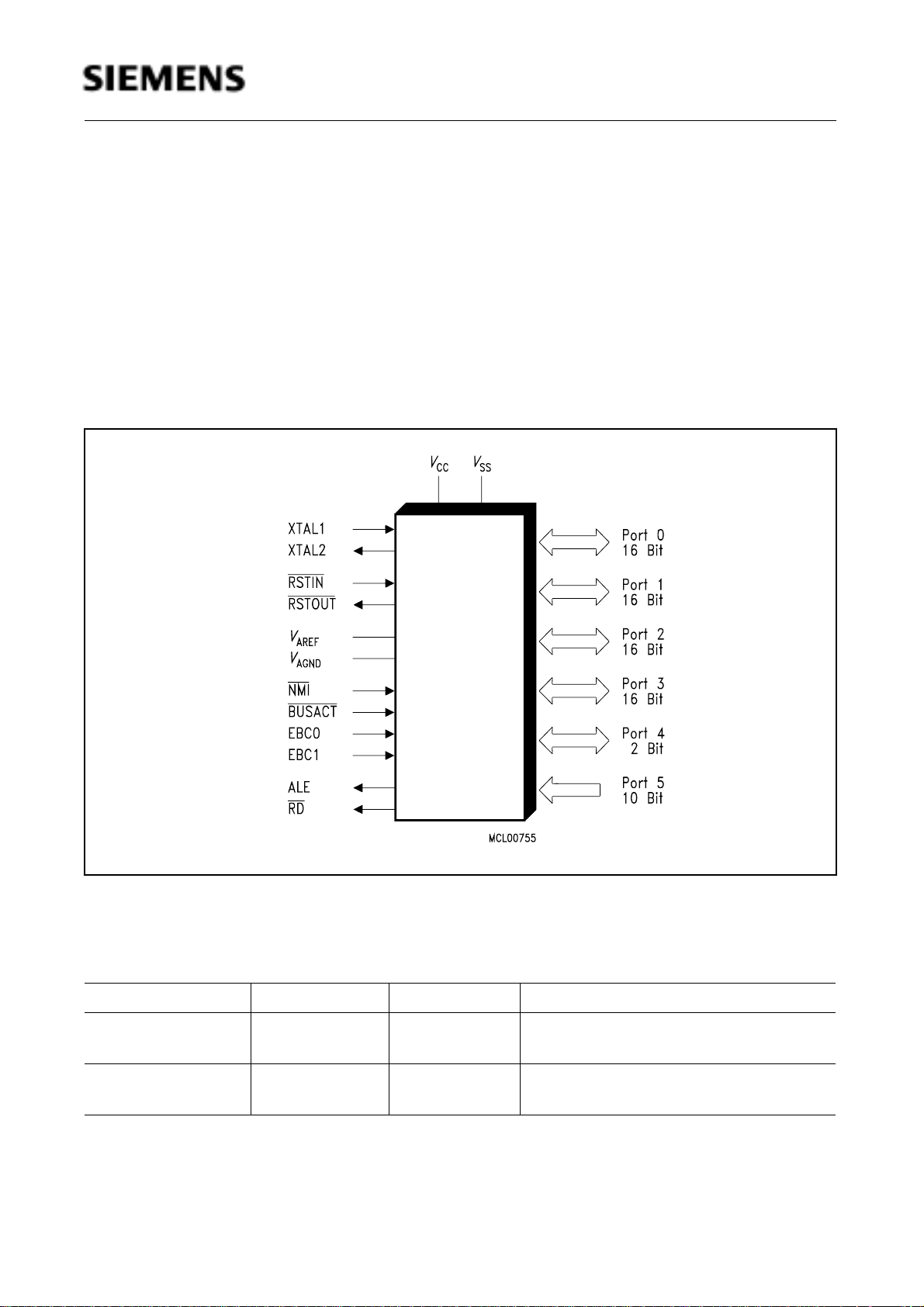
Figure 1
Logic Symbol
Ordering Information
Type Ordering Code Package Function
SAB 88C166-5M Q67120-C850 P-MQFP-100 16-bit microcontroller, 0 ˚C to + 70 ˚C,
1 KByte RAM, 32 KByte Flash EPROM
SAB 88C166W-5M Q67120-C934 P-MQFP-100 16-bit microcontroller, 0 ˚C to + 70 ˚C,
1 KByte RAM, 32 KByte Flash EPROM
Semiconductor Group 2
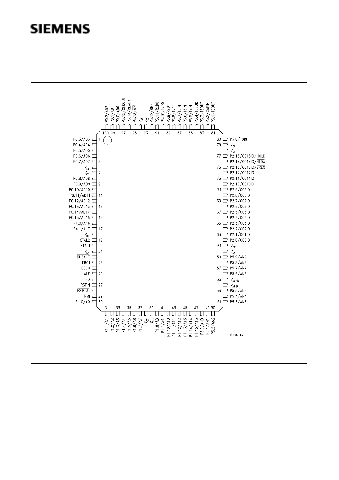
Pin Configuration Rectangular P-MQFP-100 (top view)
SAB 88C166(W)
Figure 2
SAB 88C166(W)
VPP /
Semiconductor Group 3

Pin Definitions and Functions
SAB 88C166(W)
Symbol Pin
Number
P4.0 –
16 - 17
P4.1
16
17
XTAL1
XTAL2
BUSACT
EBC1,
EBC0
V
PP
RSTIN
RSTOUT
20
19
22
,
23
24
23
27 I Reset Input with Schmitt-Trigger characteristics. A low level at
28 O Internal Reset Indication Output. This pin is set to a low level
Input (I)
Output (O)
I/O
O
O
I
O
I
I
I
Function
Port 4 is a 2-bit bidirectional I/O port. It is bit-wise
programmable for input or output via direction bits. For a pin
configured as input, the output driver is put into highimpedance state.
In case of an external bus configuration, Port 4 can be used to
output the segment address lines:
P4.0 A16 Least Significant Segment Addr. Line
P4.1 A17 Most Significant Segment Addr. Line
XTAL1: Input to the oscillator amplifier and input to the
internal clock generator
XTAL2: Output of the oscillator amplifier circuit.
To clock the device from an external source, drive XTAL1,
while leaving XTAL2 unconnected. Minimum and maximum
high/low and rise/fall times specified in the AC Characteristics
must be observed.
External Bus Configuration selection inputs. These pins are
sampled during reset and select either the single chip mode
or one of the four external bus configurations:
BUSACT
EBC1 EBC0 Mode/Bus Configuration
0 0 0 8-bit demultiplexed bus
0 0 1 8-bit multiplexed bus
0 1 0 16-bit muliplexed bus
0 1 1 16-bit demultiplexed bus
1 0 0 Single chip mode
1 0 1 Reserved.
1 1 0 Reserved.
1 1 1 Reserved.
After reset pin EBC1 accepts the programming voltage for the
Flash EPROM as an “alternate function”:
Flash EPROM Programming Voltage V
= 12 V.
PP
this pin for a specified duration while the oscillator is running
resets the SAB 88C166(W). An internal pullup resistor permits
power-on reset using only a capacitor connected to V
SS
.
when the part is executing either a hardware-, a software- or a
watchdog timer reset. RSTOUT remains low until the EINIT
(end of initialization) instruction is executed.
Semiconductor Group 4

Pin Definitions and Functions (cont’d)
SAB 88C166(W)
Symbol Pin
Number
NMI 29 I Non-Maskable Interrupt Input. A high to low transition at this
ALE 25 O Address Latch Enable Output. Can be used for latching the
RD
P1.0 –
P1.15
26 O External Memory Read Strobe. RD is activated for every
30 - 37
40 - 47
Input (I)
Output (O)
I/O Port 1 is a 16-bit bidirectional I/O port. It is bit-wise
Function
pin causes the CPU to vector to the NMI trap routine. When
the PWRDN (power down) instruction is executed, the NMI
pin must be low in order to force the SAB 88C166(W) to go
into power down mode. If NMI is high, when PWRDN is
executed, the part will continue to run in normal mode.
If not used, pull NMI high externally.
address into external memory or an address latch in the
multiplexed bus modes.
external instruction or data read access.
programmable for input or output via direction bits. For a pin
configured as input, the output driver is put into highimpedance state. Port 1 is used as the 16-bit address bus (A)
in demultiplexed bus modes and also after switching from a
demultiplexed bus mode to a multiplexed bus mode..
P5.0 –
P5.9
P2.0 –
P2.15
48 – 53
56 – 59II
62 – 77
62
...
75
76
77
I/O
I/O
I/O
O
I/O
O
I/O
I
Port 5 is a 10-bit input-only port with Schmitt-Trigger
characteristics. The pins of Port 5 also serve as the (up to 10)
analog input channels for the A/D converter, where P5.x
equals ANx (Analog input channel x).
Port 2 is a 16-bit bidirectional I/O port. It is bit-wise
programmable for input or output via direction bits. For a pin
configured as input, the output driver is put into highimpedance state.
The following Port 2 pins also serve for alternate functions:
P2.0 CC0IO CAPCOM: CC0 Cap.-In/Comp.Out
... ... ...
P2.13 CC13IO CAPCOM: CC13 Cap.-In/Comp.Out,
BREQ
P2.14 CC14IO CAPCOM: CC14 Cap.-In/Comp.Out,
HLDA External Bus Hold Acknowl. Output
P2.15 CC15IO CAPCOM: CC15 Cap.-In/Comp.Out,
HOLD External Bus Hold Request Input
External Bus Request Output
Semiconductor Group 5

Pin Definitions and Functions (cont’d)
SAB 88C166(W)
Symbol Pin
Number
P3.0 –
P3.15
80 – 92,
95 – 97
80
81
82
83
84
85
86
87
88
89
90
91
92
95
96
97
Input (I)
Output (O)
I/O
I/O
I
O
I
O
I
I
I
I
O
I/O
O
I/O
O
O
I
O
Function
Port 3 is a 16-bit bidirectional I/O port. It is bit-wise
programmable for input or output via direction bits. For a pin
configured as input, the output driver is put into highimpedance state.
The following Port 3 pins also serve for alternate functions:
P3.0 T0IN CAPCOM Timer T0 Count Input
P3.1 T6OUT GPT2 Timer T6 Toggle Latch Output
P3.2 CAPIN GPT2 Register CAPREL Capture Input
P3.3 T3OUT GPT1 Timer T3 Toggle Latch Output
P3.4 T3EUD GPT1 Timer T3 Ext.Up/Down Ctrl.Input
P3.5 T4IN GPT1 Timer T4 Input for
Count/Gate/Reload/Capture
P3.6 T3IN GPT1 Timer T3 Count/Gate Input
P3.7 T2IN GPT1 Timer T2 Input for
Count/Gate/Reload/Capture
P3.8 TxD1 ASC1 Clock/Data Output (Asyn./Syn.)
P3.9 RxD1 ASC1 Data Input (Asyn.) or I/O (Syn.)
P3.10 T×D0 ASC0 Clock/Data Output (Asyn./Syn.)
P3.11 R×D0 ASC0 Data Input (Asyn.) or I/O (Syn.)
P3.12 BHE
Ext. Memory High Byte Enable Signal,
P3.13 WR External Memory Write Strobe
P3.14 READY Ready Signal Input
P3.15 CLKOUT System Clock Output (=CPU Clock)
P0.0 –
P0.15
V
AREF
V
AGND
98 – 5
8 – 15
I/O Port 0 is a 16-bit bidirectional IO port. It is bit-wise
programmable for input or output via direction bits. For a pin
configured as input, the output driver is put into highimpedance state.
In case of an external bus configuration, Port 0 serves as the
address (A) and address/data (AD) bus in multiplexed bus
modes and as the data (D) bus in demultiplexed bus modes.
Demultiplexed bus modes:
Data Path Width: 8-bit 16-bit
P0.0 – P0.7: D0 – D7 D0 - D7
P0.8 – P0.15: output! D8 - D15
Multiplexed bus modes:
Data Path Width: 8-bit 16-bit
P0.0 – P0.7: AD0 – AD7 AD0 - AD7
P0.8 – P0.15: A8 - A15 AD8 - AD15
54 - Reference voltage for the A/D converter.
55 - Reference ground for the A/D converter.
Semiconductor Group 6

Pin Definitions and Functions (cont’d)
SAB 88C166(W)
Symbol Pin
Number
V
CC
7, 18,
38, 61,
79, 93
V
SS
6, 21,
39, 60,
78, 94
Input (I)
Function
Output (O)
- Digital Supply Voltage:
+ 5 V during normal operation and idle mode.
≥ 2.5 V during power down mode
- Digital Ground.
Functional Description
This document only describes specific properties of the SAB 88C166(W), e.g. Flash memory
functionality or specific DC and AC Characteristics, while for all other descriptions common for the
SAB 88C166(W) and the SAB 80C166(W)/83C166(W), e.g. functional description, it refers to the
respective Data Sheet for the Non-Flash device.
A detailled description of the SAB 88C166(W)’s instruction set can be found in the “C16x Family
Instruction Set Manual”.
Semiconductor Group 7

SAB 88C166(W)
Memory Organization
The memory space of the SAB 88C166(W) is configured in a Von Neumann architecture which
means that code memory, data memory, registers and I/O ports are organized within the same
linear address space which includes 256 KBytes. Address space expansion to 16 MBytes is
provided for future versions. The entire memory space can be accessed bytewise or wordwise.
Particular portions of the on-chip memory have additionally been made directly bit addressable.
1 KByte of on-chip RAM is provided as a storage for user defined variables, for the system stack,
general purpose register banks and even for code. A register bank can consist of up to 16 wordwide
(R0 to R15) and/or bytewide (RL0, RH0, …, RL7, RH7) so-called General Purpose Registers
(GPRs).
512 bytes of the address space are reserved for the Special Function Register area. SFRs are
wordwide registers which are used for controlling and monitoring functions of the different on-chip
units. 98 SFRs are currently implemented. Unused SFR addresses are reserved for future
members of the SAB 80C166 family.
In order to meet the needs of designs where more memory is required than is provided on chip, up
to 256 KBytes of external RAM and/or ROM can be connected to the microcontroller.
Flash Memory Overview
The SAB 88C166(W) provides 32 KBytes of electrically erasable and reprogrammable non-volatile
Flash EPROM on-chip for code or constant data, which can be mapped to either segment 0
(0’0000H to 0’7FFFH) or segment 1 (1’0000H to 1’7FFFH) during the initialization phase.
A separate Flash Control Register (FCR) has been implemented to control Flash operations like
programming or erasure. For programming or erasing an external 12 V programming voltage must
be applied to the VPP/EBC1 pin.
The Flash memory is organized in 8 K x 32 bits, which allows even double-word instructions to be
fetched in just one machine cycle. The entire Flash memory is divided into four blocks with different
sizes (12/12/6/2 KByte). This allows to erase each block separately, when only parts of the Flash
memory need to be reprogrammed. Word or double word programming typically takes 100 µs, block
erasing typically takes 1 s (@ 20 MHz CPU clock). The Flash memory features a typical endurance
of 100 erasing/programming cycles. Erased Flash memory cells contain all ‘1’s, as known from
standard EPROMs.
The Flash memory can be programmed both in an appropriate programming board and in the target
system, which provides a lot of flexibility. The SAB 88C166(W)’s on-chip bootstrap loader may be
used to load and start the programming code.
To save the customer’s know-how, a Flash memory protection option is provided in the SAB
88C166(W). If this was activated once, Flash memory contents cannot be read from any location
outside the Flash memory itself.
Semiconductor Group 8

SAB 88C166(W)
3’FFFF
3’0000
2’0000
1’0000
0’0000
H
3
H
Bank 3
Bank 2
2
Bank 1
H
1
H
Bank 0
0
H
Memory Segments Flash Banks
x’7800
x’6000
x’3000
x’0000
H
H
H
H
Figure 3
Flash Memory Overview
The Flash Control Register (FCR)
In standard operation mode the Flash memory can be accessed like the normal maskprogrammable on-chip ROM of the SAB 83C166. So all appropriate direct and indirect addressing
modes can be used for reading the Flash memory.
All programming or erase operations of the Flash memory are controlled via the 16-bit Flash control
register FCR. To prevent unintentional writing to the Flash memory the FCR is locked and inactive
during standard operation mode. Before a valid access to the FCR is enabled, the Flash memory
writing mode must be entered. This is done via a special key code instruction sequence.
Semiconductor Group 9

SAB 88C166(W)
FCR (FFA0H / D0H) SFR Reset Value: 00X0
5 4 3 2 1 011 10 9 8 7 615 14 13 12
FWM
SET
rw
rw-rw-rw-rw-rw
- FWE
BE
WDW
W
CKCTL
VPP
REVFCVPP
FBUSY
RPROT
FEE
rw
*)
H
rwrw rrw rw r/wrw
Bit Function
FWE Flash Write Enable Bit (see description below)
0 : Flash write operations (program / erase) disabled
1 : Flash write operations (program / erase) enabled
FEE Flash Erase Enable Bit (Significant only, when FWE = ’1’, see description below)
0 : Flash programming mode selected
1 : Flash erase mode selected
FBUSY
Flash Busy Bit (On read accesses)
0 : No Flash write operation in progress
1 : Flash write operation in progress
RPROT
Flash Read Protection Activation Bit (On write accesses)
0 : Deactivates Flash read protection
1 : Activates Flash read protection, if this is enabled
FCVPP Flash Control V
PP
Bit
0 : No VPP failure occurred during a Flash write operation
1 : VPP failure occurred during a Flash write operation
VPPREV Flash V
0 : No valid VPP applied to pin V
Revelation Bit
PP
PP
1 : VPP applied to pin VPP is valid
CKCTL Internal Flash Timer Clock Control
Determines the width of an internal Flash write or erase pulse
WDWW Word / Double Word Writing Bit (significant only in programming mode)
0 : 16-bit programming operation
1 : 32-bit programming operation
BE Bank Erase Select (significant only in erasing mode)
Selects the Flash Bank to be erased
FWMSET Flash Writing Mode Set Bit (see description below)
0 : Exit Flash writing mode, return to standard mode
1 : Stay in Flash writing mode
*)
The reset value of bit VPPREV depends on the voltage on pin VPP.
Note: The FCR is no real register but is rather virtually mapped into the active address space of the
Flash memory while the Flash writing mode is active. In writing mode all direct (mem)
accesses refer to the FCR, while all indirect ([Rwn]) accesses refer to the Flash memory
array itself.
Semiconductor Group 10

SAB 88C166(W)
The selection of Flash Operation and Read Mode is done via the three bits FWE, FEE and
FWMSET. The table below shows the combinations for these bits to select a specific function:
FWMSET FEE FWE Flash Operation Mode Flash Read Mode
1 1 1 Erasing mode Erase-Verify-Read via [Rn]
1 0 1 Programming mode Program-Verify-Read via [Rn]
1 X 0 Non-Verify mode Normal Read via [Rn]
0 X X Standard mode Normal Read via [Rn] or mem
FWE enables/disables write operations, FEE selects erasing or programming, FWMSET controls
the writing mode. Bits FWE and FEE select an operation, but do not execute it directly.
Note: Watch the FWMSET bit, when writing to register FCR (word access only), in order not to exit
Flash writing mode unintentionally by clearing bit FWMSET.
FBUSY: This read-only flag is set to ‘1’ while a Flash programming or erasing operation is in
progress. FBUSY is set via hardware, when the respective command is issued.
RPROT: This write-only Flash Read Protection bit determines whether Flash protection is active
or inactive. RPROT is the only FCR bit which can be modified even in the Flash standard mode but
only by an instruction executed from the on-chip Flash memory itself. Per reset, RPROT is set to ‘1’.
Note: RPROT is only significant, if the general Flash memory protection is enabled.
V
FCVPP and VPPREV: These read-only bits allow to monitor the
Revelation bit VPPREV reflects the state of the
‘0’ indicates that
V
is below the threshold value necessary for reliable programming or erasure,
PP
otherwise VPPREV = ‘1’). The Flash Control
V
voltage in the Flash writing mode (VPPREV =
PP
V
bit FCVPP indicates, if
PP
voltage. The Flash Vpp
PP
V
fell below the valid
PP
threshold value during a Flash programming or erase operation (FCVPP = ‘1’). FCVPP = ‘0’ after
such an operation indicates that no critical discontinuity on
V
has occurred.
PP
CKCTL: This Flash Timer Clock Control bitfield controls the width of the programming or erase
pulses (TPRG) applied to Flash memory cells during the corresponding operation. The width of a
single programming or erase pulse and the cumulated programming or erase time must not exceed
certain values to avoid putting the Flash memory under critical stress (see table below).
Time Specification Limit Value
Maximum Programming Pulse Width
Maximum Cumulated Programming Time
Maximum Erase Pulse Width
Maximum Cumulated Erase Time
128 µs
2.5 ms
10 ms
30 s
Semiconductor Group 11
SAB 88C166(W)
In order not to exceed the limit values listed above, a specific CKCTL setting requires a minimum
CPU clock frequency, as listed below.
Setting of
CKCTL
0 0 2
0 1 2
1 0 2
1 1 2
Length of
TPRG
7
* 1/f
CPU
11
* 1/f
CPU
15
* 1/f
CPU
18
* 1/f
CPU
TPRG
@ f
CPU
= 20 MHz
f
CPUmin
for programming
f
CPUmin
for erasing
6.4 µs 1 MHz ---
102.4 µs 16 MHz 1 MHz
1.64 ms --- 3.28 MHz
13.11 ms --- 13.11 MHz
The maximum number of allowed programming or erase attempts depends on the CPU clock
frequency and on the CKCTL setting chosen in turn. This number results from the actual pulse width
compared to the maximum pulse width (see above tables).
The table below lists some sample frequencies, the respective recommended CKCTL setting and
the resulting maximum number of program / erase pulses:
f
CPU
CKCTL TPROG N
Programming Erasing
PROGmax
CKCTL TPROG N
ERASEmax
1 MHz 0 0 128 µs 19 0 1 2.05 ms 14648
10 MHz 0 0 12.8 µs 195 1 0 3.28 ms 9155
16 MHz 0 0 8 µs 312 1 0 2.05 ms 14648
20 MHz 0 0 6.4 µs 390 1 0 1.64 ms 18310
BE: The Flash Bank Erasing bit field determines the Flash memory bank to be erased (see table
below). The physical addresses of the selected bank depend on the Flash memory mapping
chosen.
BE setting Bank Addresses Selected for Erasure (x = 0 or 1)
0 0
0 1
1 0
1 1
0
1
2
3
x’0000
to x’2FFF
H
x’3000H to x’5FFF
x’6000H to x’77FF
x’7800H to x’7FFF
H
H
H
H
Semiconductor Group 12
SAB 88C166(W)
Operation Modes of the Flash Memory
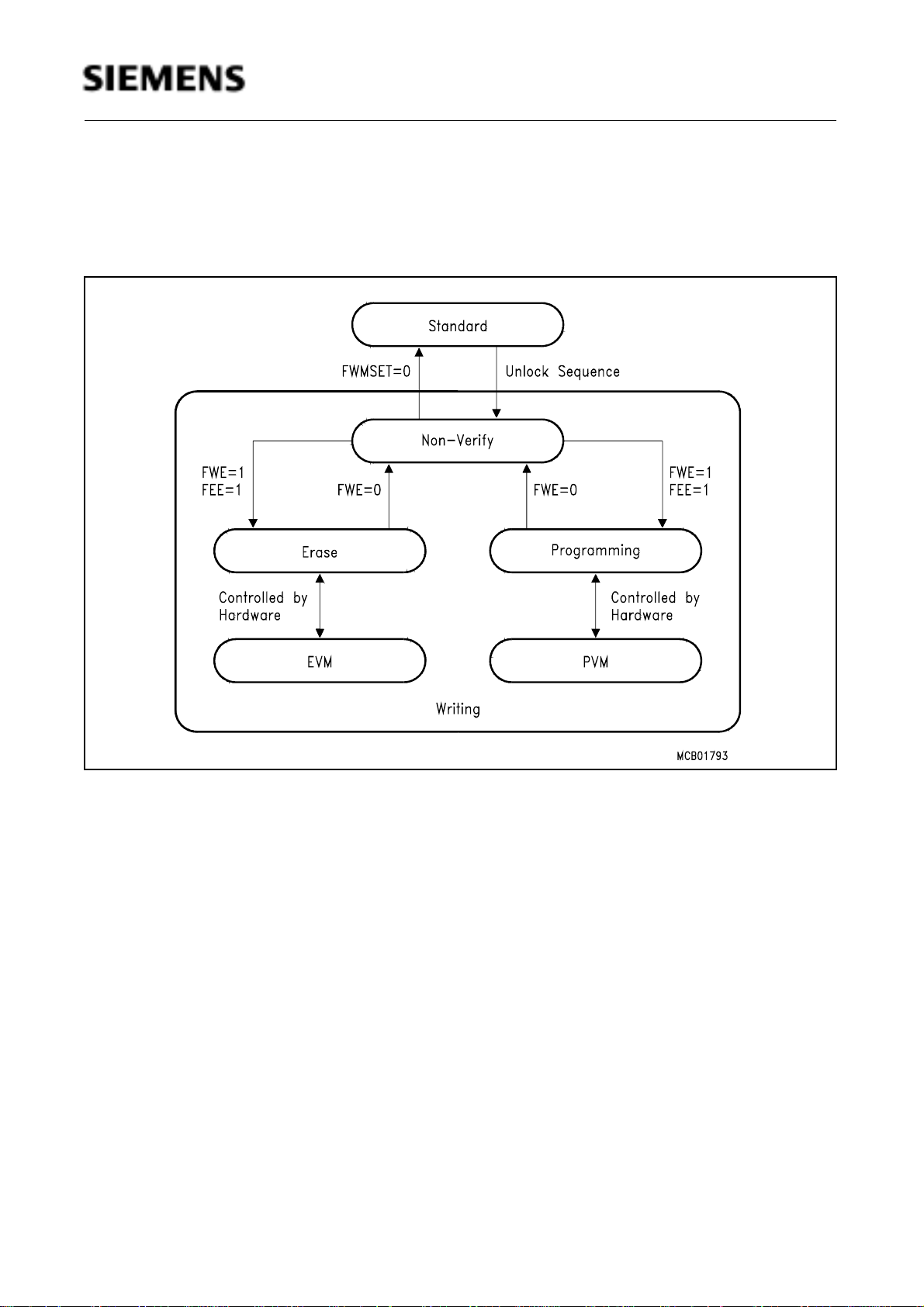
There are two basic operation modes for Flash accesses: The standard and the writing mode. Submodes of the writing mode are the programming, the erase and the non-verify mode.
Figure 4
Flash Operating Mode Transitions
In Standard Mode the Flash memory can be accessed from any memory location (external
memory, on-chip RAM or Flash memory) for instruction fetches and data operand reads. Data
operand reads may use both direct 16-bit (mnemonic: mem) and indirect (mnemonic: [Rw])
addressing modes. Standard mode does not allow accesses to the FCR or Flash write operations.
Note: When Flash protection is active, data operands can be accessed only by instructions that are
executed out of the internal Flash memory.
The Flash Writing Modes must be entered for programming or erasing the Flash memory. The
SAB 88C166 enters these modes by a specific key code sequence, called UNLOCK sequence.
In writing mode the used addressing mode decides whether the FCR or a Flash memory location is
accessed. The FCR can be accessed with any direct access to an even address in the active
address space of the Flash memory. Only word operand instructions are allowed for FCR accesses.
Accesses to Flash memory locations must use indirect addressing to even addresses.
direct 16-bit addressing mode: mem --> Access to FCR
indirect addressing mode: [Rw
] --> Access to Flash location
n
Semiconductor Group 13

SAB 88C166(W)
After entering writing mode the first erase or programming operation must not be started for at least
10 µs. This absolute (!) delay time is required to set up the internal high voltage. In general, Flash
write operations need a 12 V external
It is not possible to erase or to program the Flash memory via code executed from the Flash memory
itself. The respective code must reside within the on-chip RAM or within external memory.
When programming or erasing ‘on-line’ in the target system, some considerations have to be taken:
While these operations are in progress, the Flash memory cannot be accessed as usual. Therefore
care must be taken that no branch is taken into the Flash memory and that no data reads are
attempted from the Flash memory during programming or erasure. If the Flash memory is mapped
to segment 0, it must especially be ensured that no interrupt or hardware trap can occur, because
this would implicitly mean such a ‘forbidden’ branch to the Flash memory in this case.
The UNLOCK sequence is a specific key code sequence, which is required to enable the writing
modes of the SAB 88C166(W). The UNLOCK sequence must use identical values (see example
below) and must not be interrupted:
V
voltage to be applied to the
PP
V
PP
/EBC1 pin.
MOV FCR, Rw
MOV [Rw
], Rw
n
n
n
; Dummy write to the FCR
; Both operands use the same GPR
CALL cc_UC, WAIT_10 ; Delay for 10 µs (may be realized also by
; instructions other than a delay loop
where Rw
can be any word GPR (R0…R15). [Rwn] and FCR must point to even addresses within
n
the active address space of the Flash memory.
Note: Data paging and Flash segment mapping, if active, must be considered in this context.
In Flash Erase Mode (FEE=’1’, FWE=’1’) the SAB 88C166(W) is prepared to erase the bank
selected by the Bank Erase (BE) bit field in the FCR. The width of the erase pulses generated
internally is defined by the Internal Flash Timer Clock Control (CKCTL) bit field of the FCR. The
maximum number of erase pulses (EN
in the Flash erase algorithm. The chosen values for CKCTL and EN
) applied to the Flash memory is determined by software
max
must guarantee a maximum
max
cumulated erase time of 30 s per bank and a maximum erase pulse width of 20 ms.
The Flash bank erase operation will not start before the erase command is given. This provides
additional security for the erase operation. The erase command can be any write operation to a
Flash location, where the data and the even address written to must be identical:
MOV [Rwn], Rw
n
; Both operands use the same GPR
Upon the execution of this instruction, the Flash Busy (FBUSY) flag is automatically set to ‘1’
indicating the start of the operation. End of erasure can be detected by polling the FBUSY flag.
V
PP
must stay within the valid margins during the entire erase process.
At the end of erasure the Erase-Verify-Mode (EVM) is entered automatically. This mode allows to
check the effect of the erase operation (see description below).
Note: Before the erase algorithm can be properly executed, the respective bank of the Flash
memory must be programmed to all zeros (‘0000H’).
Semiconductor Group 14

SAB 88C166(W)
In Flash Programming Mode (FEE=’0’, FWE=’1’) the SAB 88C166(W) is prepared to program
Flash locations in the way specified by the Word or Double Word Write (WDWW) bit in the FCR. The
width of the programming pulses generated internally is defined by the Internal Flash Timer Clock
Control (CKCTL) bit field of the FCR. The maximum number of programming pulses (PN
applied to the Flash memory is determined by software in the Flash programming algorithm. The
chosen values for CKCTL and PN
must guarantee a maximum cumulated programming time of
max
2.5 ms per cell and a maximum programming pulse width of 200 µs.
If 16-bit programming was selected, the operation will start automatically when an instruction is
executed, where the first operand specifies the address and the second operand the value to be
programmed:
max
)
MOV [Rwn], Rw
m
; Program one word
If 32-bit programming was selected, the operation will start automatically when the second of two
subsequent instructions is executed, which define the doubleword to be programmed. Note that the
destination pointers of both instructions refer to the same even double word address. The two
instructions must be executed without any interruption.
MOV [Rw
MOV [Rw
], Rw
n
], Rw
n
x
y
; Prepare programming of first word
; Start programming of both words
Upon the execution of the second instruction (the one and only in 16-bit programming mode), the
Flash Busy (FBUSY) bit is automatically set to ‘1’. End of programming can be detected by polling
the FBUSY bit.
V
must stay within the valid margins during the entire programming process.
PP
At the end of programming the Program-Verify-Mode (PVM) is entered automatically. This mode
allows to check the effect of the erase operation (see description below).
The Flash Verify-Modes Erase-Verify-Mode (EVM) and Program-Verify-Mode (PVM) allow to
verify the effect of an erase or programming operation. In these modes an internally generated
margin voltage is applied to a Flash cell, which makes reading more critical than for standard read
accesses. This ensures safe standard accesses after correct verification.
To get the contents of a Flash word in this mode, it has to be read in a particular way:
MOV Rw
, [Rwn] ; First (invalid) read of dedicated cell
m
… ; 4 µs delay to stabilize internal margin voltage
MOV Rw
, [Rwn] ; Second (valid) read of dedicated cell
m
Such a Flash verify read operation is different from the reading in the standard or in the non-verify
mode. Correct verify reading needs a read operation performed twice on the same cell with an
absolute time delay of 4 µs which is needed to stabilize the internal margin voltage applied to the
cell. To verify that a Flash cell was erased or programmed properly, the value of the second verify
read operation has to be compared against FFFFH or the target value, respectively. Clearing bit
FWE to ‘0’ exits the Flash programming mode and returns to the Flash non-verify mode.
In Flash non-verify mode all Flash locations can be read as usual (via indirect addressing modes),
which is not possible in Flash programming or Flash erase mode (see EVM and PVM).
Semiconductor Group 15

SAB 88C166(W)
Flash Protection
If active, Flash protection prevents data operand accesses and program branches into the on-chip
Flash area from any location outside the Flash memory itself. Data operand accesses and branches
to Flash locations are exclusively allowed for instructions executed from the Flash memory itself.
Erasing and programming of the Flash memory is not possible while Flash protection is active.
Note: A program running within the Flash memory may of course access any location outside the
Flash memory and even branch to a location outside.
However, there is no way back, if Flash protection is active.
Flash protection is controlled by two different bits:
• The user-accessible write-only Protection Activation bit (RPROT) in register FCR and
• The one-time-programmable Protection Enable bit (UPROG).
Bit UPROG is a ‘hidden’ one-time-programmable bit only accessible in a special mode, which can
be entered eg. via a Flash EPROM programming board. Once programmed to ‘1’, this bit is
unerasable, ie. it is not affected by the Flash Erase mechanism.
To activate Flash Protection bit UPROG must have been programmed to ‘1’, and bit RPROT in
register FCR must be set to ‘1’. Both bits must be ‘1’ to activate Flash protection.
To deactivate Flash Protection bit RPROT in register FCR must be cleared to ‘0’. If any of the two
bits (UPROG or RPROT) is ‘0’, Flash protection is deactivated.
Generally Flash protection will remain active all the time. If it has to be deactivated intermittently, eg.
to call an external routine or to reprogram the Flash memory, bit RPROT must be cleared to ‘0’.
To access bit RPROT in register FCR, an instruction with a ‘mem, reg’ addressing mode must be
used, where the first operand has to represent the FCR address (any even address within the active
address space of the Flash memory) and the second operand must refer to a value which sets the
RPROT bit to ‘0’, eg.:
MOV FCR, ZEROS ; Deactivate Flash Protection
RPROT is the only bit in the FCR which can be accessed in Flash standard mode without having to
enter the Flash writing mode. Other bits in the FCR are not affected by such a write operation.
However, this access requires an instruction executed out of the internal Flash memory itself.
After reset bit RPROT is set to ’1’. For devices with protection disabled (UPROG=’0’) this has no
effect. For devices with protection enabled this ensures that program execution starts with Flash
protection active from the beginning.
Note: In order to maintain uninterrupted Flash protection, be sure not to clear bit RPROT
unintentionally by FCR write operations. Otherwise the Flash protection is deactivated.
Semiconductor Group 16
SAB 88C166(W)
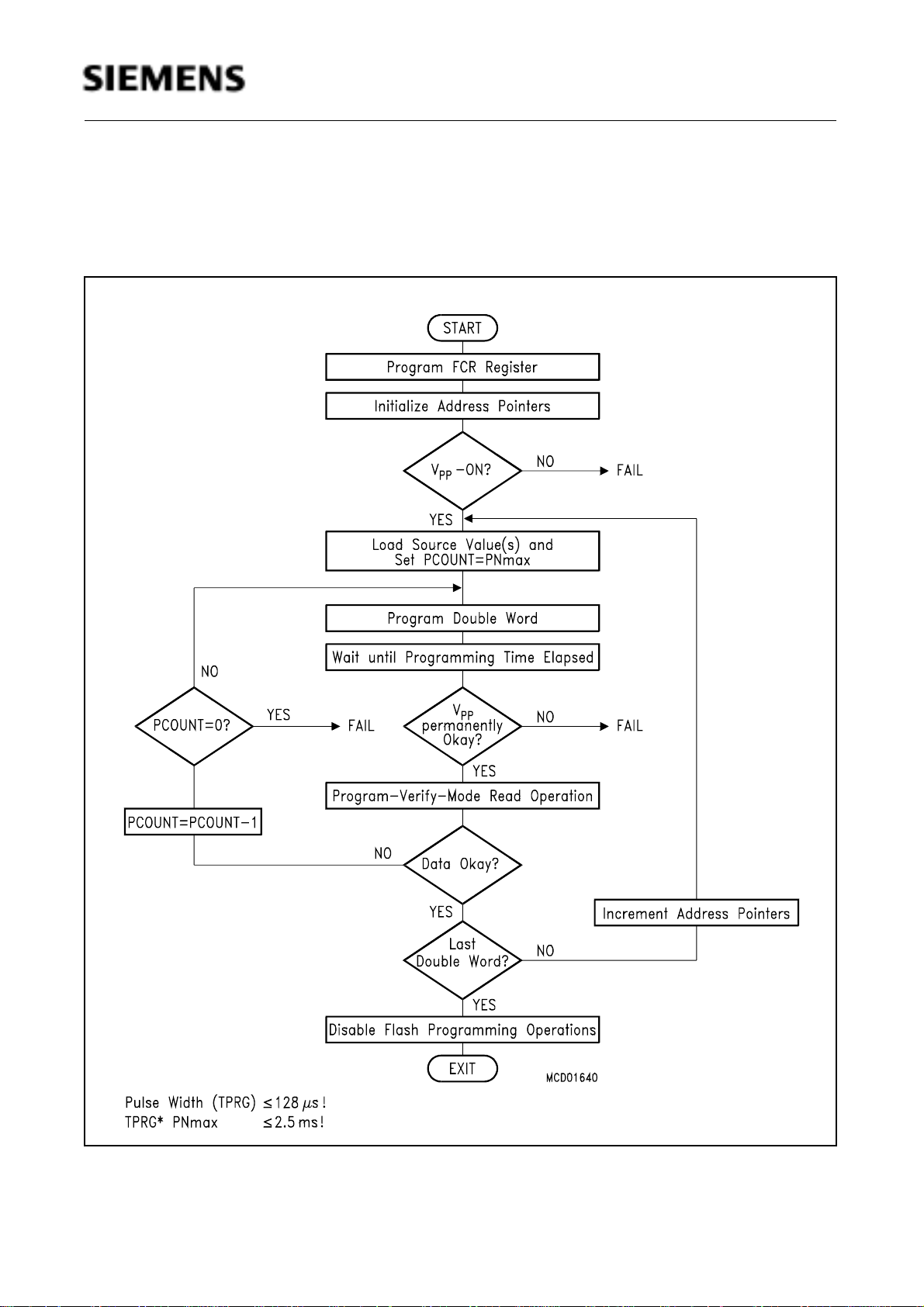
Flash Programming Algorithm
The figure below shows the recommended Flash programming algorithm. The following example
describes this algorithm in detail.
Figure 5
Flash Programming Algorithm
Semiconductor Group 17
 Loading...