

Page 1

Introduction
The Pocket Guide CPU 922/CPU 928/CPU 928B/
CPU 948
Order No. 6ES5 997-3UA22
is included with this manual.
1
SIMATIC S5
S5-155U
CPU 948
Programming Guide
Order No. 6ES5 998-3PR21
Release 03
User Program
Program Execution
Operating Sta tuses and Pr ogram
Execution Levels
Interrupt and Error Diagnosis
Integrated Special Functions
Extended Data Block DX 0
Memory Assignment and
Memory Organization
2
3
4
5
6
7
8
Memory Access Using
Absolute Addresses
Multiprocessor Mode and
Communication in the S5-155U
PG Interfaces and
Functions
Appendix
Further Reading
List of Abbreviations,
List of Key Words,
List of Tables and Figures
9
10
11
12
13
14
C79000-H8576-C848-03
Page 2

Copyright
Copyright © Siemens AG 1993 All Rights Reserved
The reprod uction , transm issio n or use of th is doc ument or it s conten ts is no t permitt ed witho ut expr ess
written authority.
Offenders wi ll b e li able for dama ges. Al l ri ghts , in clud ing righ ts c reat ed b y pa tent grant or regi stra tion of a
utility mod el or de sign, ar e reserv ed.
Disclaimer of liability
We have chec ked th e conten ts of this manual for agree ment wit h the hard ware an d softwar e descri bed.
Since dev iation s cann ot be prec luded en tirely , we cann ot guara ntee ful l agreem ent. How ever, the data in
this manual are reviewed regularly and any necessary corrections included in subsequent editions. Suggestions for improvement are welcomed.
Technica l da ta s ubje ct t o ch ange.
Safety-relate d guidelines
This manu al c onta ins noti ces whi ch y ou s houl d obse rve to e nsur e yo ur ow n pers on al s afet y, as wel l
as to protec t the prod uct and co nnec ted equi pment. Th ese noti ces ar e highli ghted in the manu al by
a warning tri angle and ar e marked as follow s accord ing to the level of da nger:
Warning
indicat es that de ath, sev ere pers onal injury or substan tial pro perty da mage ca n result
if proper precautions are not taken.
!
Caution
indicat es t hat m inor p erso nal inju ry o r prop erty dama ge c an r esul t if p rope r
precautions are not taken.
!
Only qualif ied pers onne l should be allo wed to in stall an d work on this equi pment. Q ualifi ed perso ns
are defined as persons who are authorized to commission, to ground and to tag equipment, systems
and circui ts in ac cordan ce with establi shed s afety pr actice s and st andard s.
Siemens Aktiengesellschaft
6ES5 998-3PR21
EWK Elektronikwerk Karlsruhe
Printed in the Federal Republic of Germany
Page 3

How to Use this Manual
Scope
This programming guide describes the following versions of the
CPU 948 and its system software:
Versions of the CPU 948
•• CPU 948-1 with 640 Kbytes of user memory,
Order no . 6ES5 948-3UA11, from vers ion A03
•• CPU 948-2 with 1 664 Kbytes of user memory,
Order no . 6ES5 948-3UA21, from version A03
CPU 948 Programming Guide
C79000-H8576-C848-03
0 - 1
Page 4

How to Use this Manual
Overview of the Chapters
Chapter 1
Chapter 2
Chapter 3
This informs you about the area s of app lica tion of the S5-1 55U
programmable controller with the CPU 948 and its device structur e.
It explains the typical mode of operation of the CPU and illustrates
how a CPU program i s str uc tured.
The chapter also conta ins sugge stions a bout ho w to tackle
programming an d whic h ch ar ac teristics of the CPU 948 are impor tan t
for programming.
If you have already worke d with the CPU 946/94 7 an d want to know
the differences betwe en these CPUs and the CPU 948 you will find
this information in this chapter.
This explains the components of a STE P 5 user pr ogra m an d how the
program can be structured.
This is intended for readers who do not yet have muc h expe rie nc e of
using the STEP 5 programm ing la ngua ge . It therefore deal s with the
basics of STEP 5 programming and ex pla ins the STEP 5 operations in
detail (with examples).
Experience d re ad er s who may find that the information about specific
operations in the pocke t guid e i s inade qu ate , ca n use Sec tion 3.5 as a
reference section.
Chapter 4
Chapter 5
0 - 2 C79000-H8576-C848-03
This provides an overvie w of the mod es and progr am exe cu tion levels
of the CPU 948. It provides you with detailed information about
various start-up modes and the associated organization blocks in
which you can program your routines for differrent start-up situations.
The chapter also explains th e dif fe re nc es betwe en the pr ogram
execution levels "cyc lic proc essing" , "tim e-controlled processing" and
"interrupt-driven processing" and whic h blo cks are available for your
user program.
This informs you about errors to be avo ide d whe n pla nning and
writing your STEP 5 programs.
The chapter tells you about the help you can obta in fr om the syste m
program for diagnosing errors and which reactions can be expected
and informs you ab ou t the blocks in which you can prog ram reactions
to certain errors.
The chapter also explains the CPU 948 self-test.
CPU 948 Programming Guide
Page 5

How to Use this Manual
Chapter 6
Chapter 7
Chapter 8
Chapter 9
This covers the special functions integrated in the system program. It
tells you how to use the special functions and how to call and assign
parameters to the special func tion OBs. The chapte r also ex pla ins how
to recognize and deal with er ro rs in the pr ocessin g of a specia l
function.
This describes the use of data blo ck DX 0 and its structur e. The
chapter infor ms you of the significance of the variou s DX 0
parameters. Based on examples, you will lear n how to create data
block DX 0 or how to assign the parameters in a screen form.
This is a reference section for experienced system users. It provides
information about the me mo ry organ ization of the CPU 948 and
certain system data words whic h conta in information that can be
called up by the user.
This is also for experienced system user s. The cha pte r ex pla ins how to
address data in certain memory areas using absolute addresses.
Chapter 10
Chapter 11
Chapter 12
This explains when the multipro ce ssor mode ca n be used an d how
data can be exchanged between the CPUs and CPs. The chapter
provides information ab out pro gram ming for multiprocessor operatio n.
The remainder of the ch ap ter provid es detailed information and
application examples for exchanging larger amounts of data in the
multiprocessor mode (multiprocessor communication).
This tells you how to connect your CPU to a PG and the functions
provided by the PG software to test your STEP 5 prog ra m.
This contains the Appendix with tec hn ica l data (e. g. typical operation
execution times, system runtimes, memory capacity) of the CPU 948.
CPU 948 Programming Guide
C79000-H8576-C848-03
0 - 3
Page 6

How to Use this Manual
Chapter 13
Chapter 14
This lists documentation for further reading.
This is intended to help you find themes quickly and contains a list of
abbreviations and a list of keywords as well as lists of all the
numbered tables and figu re s.
CPU 948 Programming Guide
0 - 4 C79000-H8576-C848-03
Page 7

Conventions used in the text
To provide you with an over vie w of the con ten t s of the pages, the
manual uses the following conventions in addition to a 2nd and 3rd
order of titles:
How to Use this Manual
Entries in the margin
Fourth order entries
Notes
Instructions
Entries in the margin are ke ywords printed in italics on the left-h an d
edge of a page. They provide inform atio n ab out the co nte nts of on e or
more paragraphs on the page.
Fourth order entrie s ar e no t numbe red but appear in the margin in bold
face and identify a lon ge r se ctio n of text.
The following conventions are also used.
Note
Important information is indicated in this format.
Instructions (often a seque nc e of operations to be performed) ar e
represented in tables, e.g.
Step Action Result
CPU 948 Programming Guide
C79000-H8576-C848-03
1 Switch the mode selector
from RUN to STOP.
2 Hold the reset switch in t he
OVERALL RESET position;
at the same time, switch the
mode selector from STOP to
RUN and back to STOP.
The CPU is in the stop
mode. The STOP LED is lit
continuously.
An OVERALL RESET is
requested. The STOP LED
flashes quickly.
0 - 5
Page 8

How to Use this Manual
Reference tables
Specific informatio n you ma y requ ire at any time is contained in
numbered tables as shown in the fo llowin g ex am ple and can be foun d
in the list of tables (refer to Chapter 14).
Table 3-2 Binary logic operations
Operation Operand Function
A
O
I 0.0 to 12 7.7
......
Examples
AND logic operation with scan for signal state "1"
OR logic operation with scan for signal sta te "1 "
of an input in the PII
........
Examples, some of which cover several pages, are highlighted by a gray
frame. When the examples cover more than one page this is clearly
indicated.
Example 1: Call ing a n d ass i gning par a meters to a fun c tion b lock i n the
methods of representation STL and LAD/CSF in a program block
Method of representation STL
......
CPU 948 Programming Guide
0 - 6 C79000-H8576-C848-03
Page 9

Contents
Contents
1 Introduction. . . . . . . . . . . . . . . . . . . . . . . . . . . . . . . . . . . . . . . . . . . . . . . . . . . . . . . . . . . . . . . . . . . 1-3
1.1 Area of Application for the S5-155U with the CPU 948 . . . . . . . . . . . . . . . . . . . . . . . . . . . . . . . . 1-4
1.2 Typical Mode of Operation of a CPU . . . . . . . . . . . . . . . . . . . . . . . . . . . . . . . . . . . . . . . . . . . . . . . 1-6
1.3 Th e Programs in a CPU . . . . . . . . . . . . . . . . . . . . . . . . . . . . . . . . . . . . . . . . . . . . . . . . . . . . . . . . . . 1-8
1.4 Which Operands are available to the User Program?. . . . . . . . . . . . . . . . . . . . . . . . . . . . . . . . . . 1-12
1.5 How much Memory is available for the User Program? . . . . . . . . . . . . . . . . . . . . . . . . . . . . . . . 1-15
1.6 How to Tackle Programming . . . . . . . . . . . . . . . . . . . . . . . . . . . . . . . . . . . . . . . . . . . . . . . . . . . . . 1-16
1.7 Programming Tools . . . . . . . . . . . . . . . . . . . . . . . . . . . . . . . . . . . . . . . . . . . . . . . . . . . . . . . . . . . . 1-19
1.8 What is New with the CPU 948? . . . . . . . . . . . . . . . . . . . . . . . . . . . . . . . . . . . . . . . . . . . . . . . . . 1 -20
1.8.1 CPU 948, Version A01. . . . . . . . . . . . . . . . . . . . . . . . . . . . . . . . . . . . . . . . . . . . . . . . . . . . . . . . . . 1-20
1.8.2 CPU 948, Version A02 . . . . . . . . . . . . . . . . . . . . . . . . . . . . . . . . . . . . . . . . . . . . . . . . . . . . . . . . . 1-23
1.8.3 CPU 948, Version A03 and higher . . . . . . . . . . . . . . . . . . . . . . . . . . . . . . . . . . . . . . . . . . . . . . . . 1-23
1.9 Converting User Programs of the C PU 928B for the CPU 948. . . . . . . . . . . . . . . . . . . . . . . . . . 1-24
2 User Program . . . . . . . . . . . . . . . . . . . . . . . . . . . . . . . . . . . . . . . . . . . . . . . . . . . . . . . . . . . . . . . . . 2-3
2.1 STEP 5 P rogrammi ng Language . . . . . . . . . . . . . . . . . . . . . . . . . . . . . . . . . . . . . . . . . . . . . . . . . . . 2- 4
2.1.1 The LAD, CSF, STL Methods of Representation. . . . . . . . . . . . . . . . . . . . . . . . . . . . . . . . . . . . . . 2-4
2.1.2 Structured Programming . . . . . . . . . . . . . . . . . . . . . . . . . . . . . . . . . . . . . . . . . . . . . . . . . . . . . . . . . 2-5
2.1.3 STEP 5 Operations. . . . . . . . . . . . . . . . . . . . . . . . . . . . . . . . . . . . . . . . . . . . . . . . . . . . . . . . . . . . . . 2-6
2.1.4 Number Representation . . . . . . . . . . . . . . . . . . . . . . . . . . . . . . . . . . . . . . . . . . . . . . . . . . . . . . . . . . 2-8
2.1.5 STEP 5 Blocks and Storing them in Memory. . . . . . . . . . . . . . . . . . . . . . . . . . . . . . . . . . . . . . . . 2-12
2.2 Program, Organization and Sequence Blocks . . . . . . . . . . . . . . . . . . . . . . . . . . . . . . . . . . . . . . . . 2-16
2.2.1 Organization Blocks as User Interfaces. . . . . . . . . . . . . . . . . . . . . . . . . . . . . . . . . . . . . . . . . . . . . 2-18
2.2.2 Organization Blocks for Special Functions . . . . . . . . . . . . . . . . . . . . . . . . . . . . . . . . . . . . . . . . . . 2-22
2.3 Function Blocks . . . . . . . . . . . . . . . . . . . . . . . . . . . . . . . . . . . . . . . . . . . . . . . . . . . . . . . . . . . . . . . 2-23
2.3.1 Structure of Function Blocks. . . . . . . . . . . . . . . . . . . . . . . . . . . . . . . . . . . . . . . . . . . . . . . . . . . . . 2-24
CPU 948 Programming Guide
C79000-J8576-C848-03
i
Page 10

2.3.2 Programming Function Blocks . . . . . . . . . . . . . . . . . . . . . . . . . . . . . . . . . . . . . . . . . . . . . . . . . . . 2-26
2.3.3 Calling Function Blocks and Assigning Parameters to them . . . . . . . . . . . . . . . . . . . . . . . . . . . . 2-28
2.3.4 Special Function Blocks. . . . . . . . . . . . . . . . . . . . . . . . . . . . . . . . . . . . . . . . . . . . . . . . . . . . . . . . . 2-33
2.4 Data Blocks . . . . . . . . . . . . . . . . . . . . . . . . . . . . . . . . . . . . . . . . . . . . . . . . . . . . . . . . . . . . . . . . . . 2-35
2.4.1 Creating Data Blocks . . . . . . . . . . . . . . . . . . . . . . . . . . . . . . . . . . . . . . . . . . . . . . . . . . . . . . . . . . . 2-37
2.4.2 Opening Data Blocks . . . . . . . . . . . . . . . . . . . . . . . . . . . . . . . . . . . . . . . . . . . . . . . . . . . . . . . . . . . 2-38
2.4.3 Special Data Blocks . . . . . . . . . . . . . . . . . . . . . . . . . . . . . . . . . . . . . . . . . . . . . . . . . . . . . . . . . . . . 2-41
3 Program Execution. . . . . . . . . . . . . . . . . . . . . . . . . . . . . . . . . . . . . . . . . . . . . . . . . . . . . . . . . . . . . 3- 3
3.1 Principle of Program Execution. . . . . . . . . . . . . . . . . . . . . . . . . . . . . . . . . . . . . . . . . . . . . . . . . . . . 3-4
3.2 Program Organization . . . . . . . . . . . . . . . . . . . . . . . . . . . . . . . . . . . . . . . . . . . . . . . . . . . . . . . . . . . 3-5
3.3 Storing Progra m and Data Blocks . . . . . . . . . . . . . . . . . . . . . . . . . . . . . . . . . . . . . . . . . . . . . . . . . 3-10
3.4 Processing the User Program. . . . . . . . . . . . . . . . . . . . . . . . . . . . . . . . . . . . . . . . . . . . . . . . . . . . . 3 -11
3.4.1 Definition of Terms used in Program Execution. . . . . . . . . . . . . . . . . . . . . . . . . . . . . . . . . . . . . . 3-12
3.5 STEP 5 Operations with Examples . . . . . . . . . . . . . . . . . . . . . . . . . . . . . . . . . . . . . . . . . . . . . . . . 3-15
3.5.1 Basic Operations. . . . . . . . . . . . . . . . . . . . . . . . . . . . . . . . . . . . . . . . . . . . . . . . . . . . . . . . . . . . . . . 3 -19
3.5.2 Programming Examples in the STL, LAD and CSF Methods of Representation. . . . . . . . . . . . 3-34
3.5.3 Supplementary Operations. . . . . . . . . . . . . . . . . . . . . . . . . . . . . . . . . . . . . . . . . . . . . . . . . . . . . . . 3-49
3.5.4 Executive Operations. . . . . . . . . . . . . . . . . . . . . . . . . . . . . . . . . . . . . . . . . . . . . . . . . . . . . . . . . . . 3 -59
3.5.5 Semaphore Operations . . . . . . . . . . . . . . . . . . . . . . . . . . . . . . . . . . . . . . . . . . . . . . . . . . . . . . . . . . 3-75
4 Operating Statuses and Program Execution Levels . . . . . . . . . . . . . . . . . . . . . . . . . . . . . . . . . 4-3
4.1 Introduction and Overview . . . . . . . . . . . . . . . . . . . . . . . . . . . . . . . . . . . . . . . . . . . . . . . . . . . . . . . 4-4
4.2 Program Execution Levels. . . . . . . . . . . . . . . . . . . . . . . . . . . . . . . . . . . . . . . . . . . . . . . . . . . . . . . . 4-7
4.3 STOP Mode . . . . . . . . . . . . . . . . . . . . . . . . . . . . . . . . . . . . . . . . . . . . . . . . . . . . . . . . . . . . . . . . . . 4-12
4.3.1 SOFT STOP . . . . . . . . . . . . . . . . . . . . . . . . . . . . . . . . . . . . . . . . . . . . . . . . . . . . . . . . . . . . . . . . . . 4-12
4.3.2 HARD STOP . . . . . . . . . . . . . . . . . . . . . . . . . . . . . . . . . . . . . . . . . . . . . . . . . . . . . . . . . . . . . . . . . 4-16
4.3.3 OVERALL RES ET . . . . . . . . . . . . . . . . . . . . . . . . . . . . . . . . . . . . . . . . . . . . . . . . . . . . . . . . . . . . 4-17
4.4 START-UP Mode . . . . . . . . . . . . . . . . . . . . . . . . . . . . . . . . . . . . . . . . . . . . . . . . . . . . . . . . . . . . . . 4 -19
4.4.1 MANUAL and AUTOMATIC COLD RESTART . . . . . . . . . . . . . . . . . . . . . . . . . . . . . . . . . . . . 4-20
4.4.2 MANUAL and AUTOMATIC WARM RESTART . . . . . . . . . . . . . . . . . . . . . . . . . . . . . . . . . . . . 4-21
4.4.3 Comparison between COLD RESTART and WARM RESTART . . . . . . . . . . . . . . . . . . . . . . . . 4-24
4.4.4 RETENTIVE COLD RESTART. . . . . . . . . . . . . . . . . . . . . . . . . . . . . . . . . . . . . . . . . . . . . . . . . . 4-25
4.4.5 Comparison of COLD R ESTART and RETENTIVE COLD RESTART . . . . . . . . . . . . . . . . . . 4-26
4.4.6 User Interfaces for Start-Up. . . . . . . . . . . . . . . . . . . . . . . . . . . . . . . . . . . . . . . . . . . . . . . . . . . . . . 4-27
4.4.7 Extended AUTOMATIC WARM RESTART with the CPU 948 (HOT RESTART). . . . . . . . . . 4-30
4.4.8 Interruptions during START-UP . . . . . . . . . . . . . . . . . . . . . . . . . . . . . . . . . . . . . . . . . . . . . . . . . . 4-31
4.5 RUN Mode . . . . . . . . . . . . . . . . . . . . . . . . . . . . . . . . . . . . . . . . . . . . . . . . . . . . . . . . . . . . . . . . . . . 4-33
4.5.1 Cyclic Program Execution. . . . . . . . . . . . . . . . . . . . . . . . . . . . . . . . . . . . . . . . . . . . . . . . . . . . . . . 4-34
4.5.2 Specifying Time and Interrupt-Driven Program Execution . . . . . . . . . . . . . . . . . . . . . . . . . . . . . 4-36
4.5.3 Time-Controlled Program Execution. . . . . . . . . . . . . . . . . . . . . . . . . . . . . . . . . . . . . . . . . . . . . . . 4-37
4.5.4 Interrupt-Driven Program Execution. . . . . . . . . . . . . . . . . . . . . . . . . . . . . . . . . . . . . . . . . . . . . . . 4 -45
CPU 948 Programming Guide
ii C79000-J8576-C848-03
Page 11

5 Interrupt and Error Diagnostics . . . . . . . . . . . . . . . . . . . . . . . . . . . . . . . . . . . . . . . . . . . . . . . . . 5-3
5.1 Frequent Errors in the U ser Program . . . . . . . . . . . . . . . . . . . . . . . . . . . . . . . . . . . . . . . . . . . . . . . 5-4
5.2 Error Information . . . . . . . . . . . . . . . . . . . . . . . . . . . . . . . . . . . . . . . . . . . . . . . . . . . . . . . . . . . . . . . 5-5
5.3 Procedure for Error Analysis . . . . . . . . . . . . . . . . . . . . . . . . . . . . . . . . . . . . . . . . . . . . . . . . . . . . . . 5-8
5.4 Control Bits and Interrupt Stack . . . . . . . . . . . . . . . . . . . . . . . . . . . . . . . . . . . . . . . . . . . . . . . . . . . 5 -9
5.4.1 Control Bits . . . . . . . . . . . . . . . . . . . . . . . . . . . . . . . . . . . . . . . . . . . . . . . . . . . . . . . . . . . . . . . . . . 5-10
5.4.2 ISTACK Co ntent . . . . . . . . . . . . . . . . . . . . . . . . . . . . . . . . . . . . . . . . . . . . . . . . . . . . . . . . . . . . . . 5-14
5.4.3 Example of Error Diagnosis using the ISTACK. . . . . . . . . . . . . . . . . . . . . . . . . . . . . . . . . . . . . . 5-19
5.5 Error Handling Using Organization Blocks . . . . . . . . . . . . . . . . . . . . . . . . . . . . . . . . . . . . . . . . . 5-20
5.6 Causes of Error and Reactions of the CPU. . . . . . . . . . . . . . . . . . . . . . . . . . . . . . . . . . . . . . . . . . 5-23
5.6.1 OB 19: C alling a Logic Block That Is Not Loaded (KB) . . . . . . . . . . . . . . . . . . . . . . . . . . . . . . 5 -24
5.6.2 OB 19: C alling a Data Block That Is Not Loaded (KDB). . . . . . . . . . . . . . . . . . . . . . . . . . . . . . 5-24
5.6.3 OB 23/24, OB 28/29:Timeout Error (QVZ) . . . . . . . . . . . . . . . . . . . . . . . . . . . . . . . . . . . . . . . . . 5-25
5.6.4 OB 25: Addressing Error (ADF) . . . . . . . . . . . . . . . . . . . . . . . . . . . . . . . . . . . . . . . . . . . . . . . . . . 5-26
5.6.5 OB 26: Cycle Time Exceeded Error (ZYK) . . . . . . . . . . . . . . . . . . . . . . . . . . . . . . . . . . . . . . . . . 5-27
5.6.6 OB 27: (Substitution Error SUF). . . . . . . . . . . . . . . . . . . . . . . . . . . . . . . . . . . . . . . . . . . . . . . . . . 5-28
5.6.7 OB 30: Parity Error and Timeout Error in the User Memory (PARE) . . . . . . . . . . . . . . . . . . . . 5-28
5.6.8 OB 32: Load and Transfer Error (TRAF) . . . . . . . . . . . . . . . . . . . . . . . . . . . . . . . . . . . . . . . . . . . 5-2 9
5.6.9 OB 33: C ollision of Timed Interrupts Error (WEFES/WEFEH) . . . . . . . . . . . . . . . . . . . . . . . . . 5-30
5.6.10 OB 34: Error with G DB/GX DX (FEDBX) . . . . . . . . . . . . . . . . . . . . . . . . . . . . . . . . . . . . . . . . 5-32
5.6.11 OB 35: Communication Errors . . . . . . . . . . . . . . . . . . . . . . . . . . . . . . . . . . . . . . . . . . . . . . . . . . . 5 -32
5.6.12 OB 36: Error in Self-test . . . . . . . . . . . . . . . . . . . . . . . . . . . . . . . . . . . . . . . . . . . . . . . . . . . . . . . . 5-33
5.7 Self-Test . . . . . . . . . . . . . . . . . . . . . . . . . . . . . . . . . . . . . . . . . . . . . . . . . . . . . . . . . . . . . . . . . . . . . 5-3 4
5.7.1 Overview . . . . . . . . . . . . . . . . . . . . . . . . . . . . . . . . . . . . . . . . . . . . . . . . . . . . . . . . . . . . . . . . . . . . 5-34
5.7.2 Description of the Test Functions . . . . . . . . . . . . . . . . . . . . . . . . . . . . . . . . . . . . . . . . . . . . . . . . . 5-35
5.7.3 Settings . . . . . . . . . . . . . . . . . . . . . . . . . . . . . . . . . . . . . . . . . . . . . . . . . . . . . . . . . . . . . . . . . . . . . . 5-37
5.7.4 Error Handling . . . . . . . . . . . . . . . . . . . . . . . . . . . . . . . . . . . . . . . . . . . . . . . . . . . . . . . . . . . . . . . . 5-38
6 Integrated Special Functions. . . . . . . . . . . . . . . . . . . . . . . . . . . . . . . . . . . . . . . . . . . . . . . . . . . . . 6-3
6.1 Introduction . . . . . . . . . . . . . . . . . . . . . . . . . . . . . . . . . . . . . . . . . . . . . . . . . . . . . . . . . . . . . . . . . . . 6-4
6.2 OB 121: Set/Read System Time . . . . . . . . . . . . . . . . . . . . . . . . . . . . . . . . . . . . . . . . . . . . . . . . . . . 6-7
6.3 OB 122: "Disable Interrupts" On/Off . . . . . . . . . . . . . . . . . . . . . . . . . . . . . . . . . . . . . . . . . . . . . . 6-11
6.4 OB 124: Delete STEP 5 Blocks. . . . . . . . . . . . . . . . . . . . . . . . . . . . . . . . . . . . . . . . . . . . . . . . . . . 6-13
6.5 OB 125: Generate STEP 5 Blocks. . . . . . . . . . . . . . . . . . . . . . . . . . . . . . . . . . . . . . . . . . . . . . . . . 6-16
6.6 OB 12 6: Define, Transfer Process Images . . . . . . . . . . . . . . . . . . . . . . . . . . . . . . . . . . . . . . . . . . 6-19
6.7 OB 129: Battery State . . . . . . . . . . . . . . . . . . . . . . . . . . . . . . . . . . . . . . . . . . . . . . . . . . . . . . . . . . 6-24
6.8 OB 131: Delete ACCUs 1, 2, 3 and 4. . . . . . . . . . . . . . . . . . . . . . . . . . . . . . . . . . . . . . . . . . . . . . 6-25
6.9 OB 132/133: Roll-Up ACCU/Roll-Down ACCU. . . . . . . . . . . . . . . . . . . . . . . . . . . . . . . . . . . . . 6-27
6.10 OB 141: "Disable Single Cyclic Timed Interrupts" On/Off. . . . . . . . . . . . . . . . . . . . . . . . . . . . . 6-29
6.11 OB 142: "Delay All Interrupts" On/Off . . . . . . . . . . . . . . . . . . . . . . . . . . . . . . . . . . . . . . . . . . . . 6-32
CPU 948 Programming Guide
C79000-J8576-C848-03
iii
Page 12

6.12 OB 143: "Delay Single Cyclic Timed Interrupts" On/Off . . . . . . . . . . . . . . . . . . . . . . . . . . . . . . 6-35
6.13 OB 150: Set/Read System Time . . . . . . . . . . . . . . . . . . . . . . . . . . . . . . . . . . . . . . . . . . . . . . . . . . 6-38
6.14 OB 151: Set/Read Time for Clock-Controlled Interrupt . . . . . . . . . . . . . . . . . . . . . . . . . . . . . . . 6-43
6.15 OB 153: Set/Read Time for Delayed Interrupt . . . . . . . . . . . . . . . . . . . . . . . . . . . . . . . . . . . . 6-50
6.16 OB 180: Variable Data Block Access . . . . . . . . . . . . . . . . . . . . . . . . . . . . . . . . . . . . . . . . . . . . . . 6-53
6.17 OB 181: Test Data Blocks (DB/DX) . . . . . . . . . . . . . . . . . . . . . . . . . . . . . . . . . . . . . . . . . . . . . . 6-57
6.18 OB 182: Copy Data A rea. . . . . . . . . . . . . . . . . . . . . . . . . . . . . . . . . . . . . . . . . . . . . . . . . . . . . . . . 6-59
6.19 OB 202 to 205: Multiprocessor Communication . . . . . . . . . . . . . . . . . . . . . . . . . . . . . . . . . . . . . 6-62
6.20 OB 222: Restart Cycle Monitoring Time . . . . . . . . . . . . . . . . . . . . . . . . . . . . . . . . . . . . . . . . . . . 6-63
6.21 OB 223: Comp are St art-Up Modes . . . . . . . . . . . . . . . . . . . . . . . . . . . . . . . . . . . . . . . . . . . . . . . . 6 -64
6.22 OB 254/255: Copy/Duplicate Data Blocks . . . . . . . . . . . . . . . . . . . . . . . . . . . . . . . . . . . . . . . . . . 6-65
7 Extended Data Block DX 0 . . . . . . . . . . . . . . . . . . . . . . . . . . . . . . . . . . . . . . . . . . . . . . . . . . . . . . 7-3
7.1 Application. . . . . . . . . . . . . . . . . . . . . . . . . . . . . . . . . . . . . . . . . . . . . . . . . . . . . . . . . . . . . . . . . . . . 7-4
7.2 St ructure of DX 0. . . . . . . . . . . . . . . . . . . . . . . . . . . . . . . . . . . . . . . . . . . . . . . . . . . . . . . . . . . . . . . 7-5
7.2.1 Example of In put in DX 0 . . . . . . . . . . . . . . . . . . . . . . . . . . . . . . . . . . . . . . . . . . . . . . . . . . . . . . . . 7-7
7.3 Parameters for DX 0 . . . . . . . . . . . . . . . . . . . . . . . . . . . . . . . . . . . . . . . . . . . . . . . . . . . . . . . . . . . . 7-8
7.4 Examples of Parameter Assignment . . . . . . . . . . . . . . . . . . . . . . . . . . . . . . . . . . . . . . . . . . . . . . . 7-12
7.4.1 STEP 5 Programmi ng . . . . . . . . . . . . . . . . . . . . . . . . . . . . . . . . . . . . . . . . . . . . . . . . . . . . . . . . . . 7-12
7.4.2 Parameter Assignment using the PG Screen Form . . . . . . . . . . . . . . . . . . . . . . . . . . . . . . . . . . . . 7-14
8 Memory Assignment and Memory Organization. . . . . . . . . . . . . . . . . . . . . . . . . . . . . . . . . . . . 8-3
8.1 St ructure of the Memor y Area. . . . . . . . . . . . . . . . . . . . . . . . . . . . . . . . . . . . . . . . . . . . . . . . . . . . . 8- 4
8.2 Memory Assignment in the CPU 948 . . . . . . . . . . . . . . . . . . . . . . . . . . . . . . . . . . . . . . . . . . . . . . . 8-5
8.2.1 Memory Assignment for the System R AM . . . . . . . . . . . . . . . . . . . . . . . . . . . . . . . . . . . . . . . . . 8-6
8.2.2 Memory Assignment for the Peripherals . . . . . . . . . . . . . . . . . . . . . . . . . . . . . . . . . . . . . . . . . . 8-8
8.3 User Memory Organization in the CPU 948. . . . . . . . . . . . . . . . . . . . . . . . . . . . . . . . . . . . . . . . . 8-10
8.3.1 Block Headers in User Memory . . . . . . . . . . . . . . . . . . . . . . . . . . . . . . . . . . . . . . . . . . . . . . . . . . 8-12
8.3.2 Block Address List in Data Block DB 0 . . . . . . . . . . . . . . . . . . . . . . . . . . . . . . . . . . . . . . . . . . . . 8-13
8.3.3 RI/RJ Area . . . . . . . . . . . . . . . . . . . . . . . . . . . . . . . . . . . . . . . . . . . . . . . . . . . . . . . . . . . . . . . . . . . 8-14
8.3.4 RS/RT Area. . . . . . . . . . . . . . . . . . . . . . . . . . . . . . . . . . . . . . . . . . . . . . . . . . . . . . . . . . . . . . . . . . . 8 -15
8.3.5 Bit Assignment of the System Data Words. . . . . . . . . . . . . . . . . . . . . . . . . . . . . . . . . . . . . . . . . . 8-18
8.3.6 Addressable System Data Area . . . . . . . . . . . . . . . . . . . . . . . . . . . . . . . . . . . . . . . . . . . . . . . . . . . 8-42
CPU 948 Programming Guide
iv C79000-J8576-C848-03
Page 13

9 Memory Access Using Absolute Addresses . . . . . . . . . . . . . . . . . . . . . . . . . . . . . . . . . . . . . . . . . 9-3
9.1 Introduction . . . . . . . . . . . . . . . . . . . . . . . . . . . . . . . . . . . . . . . . . . . . . . . . . . . . . . . . . . . . . . . . . . . 9-4
9.2 Memory Access via Address in ACCU 1 . . . . . . . . . . . . . . . . . . . . . . . . . . . . . . . . . . . . . . . . . . . . 9-8
9.2.1 LIR/TIR: Loading to or Transferring from a 16-Bit Memory Area Indirectly . . . . . . . . . . . . . . . 9-9
9.2.2 Examples of Access to DW > 255 . . . . . . . . . . . . . . . . . . . . . . . . . . . . . . . . . . . . . . . . . . . . . . . . 9-15
9.2.3 LDI/TDI: Loading to or Transferring from a 32-Bit Memory Area I ndirectly . . . . . . . . . . . . . . 9-17
9.3 Transferring Memory Blocks. . . . . . . . . . . . . . . . . . . . . . . . . . . . . . . . . . . . . . . . . . . . . . . . . . . . . 9-19
9.4 Operations with the Base Address Register (BR Register) . . . . . . . . . . . . . . . . . . . . . . . . . . . . . 9-22
9.4.1 Operations for Transfer between Registers. . . . . . . . . . . . . . . . . . . . . . . . . . . . . . . . . . . . . . . . . . 9-23
9.4.2 Accessing the Local Memory . . . . . . . . . . . . . . . . . . . . . . . . . . . . . . . . . . . . . . . . . . . . . . . . . . . . 9-24
9.4.3 Accessing the Global Memory . . . . . . . . . . . . . . . . . . . . . . . . . . . . . . . . . . . . . . . . . . . . . . . . . . . 9-25
9.4.4 Accessing the Dual-Port RAM Memory . . . . . . . . . . . . . . . . . . . . . . . . . . . . . . . . . . . . . . . . . . . 9-29
10 Multiprocessor Mode and Communication in the S5-155U . . . . . . . . . . . . . . . . . . . . . . . . . . 10-3
10.1 Multiprocessor Mode. . . . . . . . . . . . . . . . . . . . . . . . . . . . . . . . . . . . . . . . . . . . . . . . . . . . . . . . . . . 10-4
10.1.1 When to use the Multiprocessor Mode . . . . . . . . . . . . . . . . . . . . . . . . . . . . . . . . . . . . . . . . . . . . . 10-4
10.1.2 What Communications Mechanisms are Available?. . . . . . . . . . . . . . . . . . . . . . . . . . . . . . . . . . . 1 0-4
10.1.3 Exchanging Data via IPC Flags. . . . . . . . . . . . . . . . . . . . . . . . . . . . . . . . . . . . . . . . . . . . . . . . . . . 10-5
10.1.4 Exchanging Data via Handling Blocks . . . . . . . . . . . . . . . . . . . . . . . . . . . . . . . . . . . . . . . . . . . . . 10-8
10.1.5 What needs to be Programmed for the Multiprocessor Mode? . . . . . . . . . . . . . . . . . . . . . . . . . . 10-9
10.1.6 How to Create Data Block DB 1. . . . . . . . . . . . . . . . . . . . . . . . . . . . . . . . . . . . . . . . . . . . . . . . . . 1 0-9
10.1.7 Starting up in the Multiprocessor Mode . . . . . . . . . . . . . . . . . . . . . . . . . . . . . . . . . . . . . . . . . . . 10-13
10.1.8 Test Mode . . . . . . . . . . . . . . . . . . . . . . . . . . . . . . . . . . . . . . . . . . . . . . . . . . . . . . . . . . . . . . . . . . . 1 0-14
10.2 Multiprocessor Communication. . . . . . . . . . . . . . . . . . . . . . . . . . . . . . . . . . . . . . . . . . . . . . . . . . 10-15
10.2.1 Introduction . . . . . . . . . . . . . . . . . . . . . . . . . . . . . . . . . . . . . . . . . . . . . . . . . . . . . . . . . . . . . . . . . 10-15
10.2.2 How the Transmitter and Receiver are Identified . . . . . . . . . . . . . . . . . . . . . . . . . . . . . . . . . . . 10-16
10.2.3 Why Data is Buffered . . . . . . . . . . . . . . . . . . . . . . . . . . . . . . . . . . . . . . . . . . . . . . . . . . . . . . . . . 10-17
10.2.4 How the Buffer is Processed and Ma naged . . . . . . . . . . . . . . . . . . . . . . . . . . . . . . . . . . . . . . . . 10-18
10.2.5 System Start-Up . . . . . . . . . . . . . . . . . . . . . . . . . . . . . . . . . . . . . . . . . . . . . . . . . . . . . . . . . . . . . . 10-21
10.2.6 Calling Communication OBs. . . . . . . . . . . . . . . . . . . . . . . . . . . . . . . . . . . . . . . . . . . . . . . . . . . . 10-22
10.2.7 How to Assign Parameters to Communication OBs. . . . . . . . . . . . . . . . . . . . . . . . . . . . . . . . . . 10-23
10.2.8 How to Evaluate the Output Parameters . . . . . . . . . . . . . . . . . . . . . . . . . . . . . . . . . . . . . . . . . . . 10-24
10.3 Runtimes of the Communication OBs. . . . . . . . . . . . . . . . . . . . . . . . . . . . . . . . . . . . . . . . . . . . . 10-31
10.4 INITIALIZE Function (OB 200). . . . . . . . . . . . . . . . . . . . . . . . . . . . . . . . . . . . . . . . . . . . . . . . . 10-33
10.4.1 Function . . . . . . . . . . . . . . . . . . . . . . . . . . . . . . . . . . . . . . . . . . . . . . . . . . . . . . . . . . . . . . . . . . . . 10-33
10.4.2 Call Parameters. . . . . . . . . . . . . . . . . . . . . . . . . . . . . . . . . . . . . . . . . . . . . . . . . . . . . . . . . . . . . . . 10-35
10.4.3 Input Parame ters. . . . . . . . . . . . . . . . . . . . . . . . . . . . . . . . . . . . . . . . . . . . . . . . . . . . . . . . . . . . . . 10-35
10.4.4 Outp ut Parameters . . . . . . . . . . . . . . . . . . . . . . . . . . . . . . . . . . . . . . . . . . . . . . . . . . . . . . . . . . . . 10-38
10.5 SEND Function (OB 202) . . . . . . . . . . . . . . . . . . . . . . . . . . . . . . . . . . . . . . . . . . . . . . . . . . . . . . 10-40
10.5.1 Function . . . . . . . . . . . . . . . . . . . . . . . . . . . . . . . . . . . . . . . . . . . . . . . . . . . . . . . . . . . . . . . . . . . . 10-40
10.5.2 Call Parameters. . . . . . . . . . . . . . . . . . . . . . . . . . . . . . . . . . . . . . . . . . . . . . . . . . . . . . . . . . . . . . . 10-40
10.5.3 Input Parame ters. . . . . . . . . . . . . . . . . . . . . . . . . . . . . . . . . . . . . . . . . . . . . . . . . . . . . . . . . . . . . . 10-40
10.5.4 Outp ut Parameters . . . . . . . . . . . . . . . . . . . . . . . . . . . . . . . . . . . . . . . . . . . . . . . . . . . . . . . . . . . . 10-42
CPU 948 Programming Guide
C79000-J8576-C848-03
v
Page 14

10.6 SEND TEST Function (OB 203) . . . . . . . . . . . . . . . . . . . . . . . . . . . . . . . . . . . . . . . . . . . . . . . . 10-45
10.6.1 Function . . . . . . . . . . . . . . . . . . . . . . . . . . . . . . . . . . . . . . . . . . . . . . . . . . . . . . . . . . . . . . . . . . . . 10-45
10.6.2 Call Parameters. . . . . . . . . . . . . . . . . . . . . . . . . . . . . . . . . . . . . . . . . . . . . . . . . . . . . . . . . . . . . . . 10-45
10.6.3 Input Parame ters. . . . . . . . . . . . . . . . . . . . . . . . . . . . . . . . . . . . . . . . . . . . . . . . . . . . . . . . . . . . . . 10-45
10.6.4 Outp ut Parameters . . . . . . . . . . . . . . . . . . . . . . . . . . . . . . . . . . . . . . . . . . . . . . . . . . . . . . . . . . . . 10-45
10.7 RECEIVE Function (OB 204). . . . . . . . . . . . . . . . . . . . . . . . . . . . . . . . . . . . . . . . . . . . . . . . . . . 10-47
10.7.1 Function . . . . . . . . . . . . . . . . . . . . . . . . . . . . . . . . . . . . . . . . . . . . . . . . . . . . . . . . . . . . . . . . . . . . 10-47
10.7.2 Call Parameters. . . . . . . . . . . . . . . . . . . . . . . . . . . . . . . . . . . . . . . . . . . . . . . . . . . . . . . . . . . . . . . 10-47
10.7.3 Input Parame ters. . . . . . . . . . . . . . . . . . . . . . . . . . . . . . . . . . . . . . . . . . . . . . . . . . . . . . . . . . . . . . 10-47
10.7.4 Outp ut Parameters . . . . . . . . . . . . . . . . . . . . . . . . . . . . . . . . . . . . . . . . . . . . . . . . . . . . . . . . . . . . 10-48
10.8 RECEIVE TEST Function (OB 205) . . . . . . . . . . . . . . . . . . . . . . . . . . . . . . . . . . . . . . . . . . . . . 10-51
10.8.1 Function . . . . . . . . . . . . . . . . . . . . . . . . . . . . . . . . . . . . . . . . . . . . . . . . . . . . . . . . . . . . . . . . . . . . 10-51
10.8.2 Call Parameters. . . . . . . . . . . . . . . . . . . . . . . . . . . . . . . . . . . . . . . . . . . . . . . . . . . . . . . . . . . . . . . 10-51
10.8.3 Input Parame ters. . . . . . . . . . . . . . . . . . . . . . . . . . . . . . . . . . . . . . . . . . . . . . . . . . . . . . . . . . . . . . 10-51
10.8.4 Outp ut Parameters . . . . . . . . . . . . . . . . . . . . . . . . . . . . . . . . . . . . . . . . . . . . . . . . . . . . . . . . . . . . 10-51
10.9 Applications . . . . . . . . . . . . . . . . . . . . . . . . . . . . . . . . . . . . . . . . . . . . . . . . . . . . . . . . . . . . . . . . . 10-53
10.9.1 Calling the Special Function OB using Function Blocks. . . . . . . . . . . . . . . . . . . . . . . . . . . . . . 10-53
10.9.2 Transferring Data Blocks. . . . . . . . . . . . . . . . . . . . . . . . . . . . . . . . . . . . . . . . . . . . . . . . . . . . . . . 10-60
10.9.3 Extending the IPCFlag Area . . . . . . . . . . . . . . . . . . . . . . . . . . . . . . . . . . . . . . . . . . . . . . . . . . . . 10-66
11 PG Interfaces and Functions . . . . . . . . . . . . . . . . . . . . . . . . . . . . . . . . . . . . . . . . . . . . . . . . . . . 11-3
11.1 Overview . . . . . . . . . . . . . . . . . . . . . . . . . . . . . . . . . . . . . . . . . . . . . . . . . . . . . . . . . . . . . . . . . . . . 11-4
11.2 PG Functions . . . . . . . . . . . . . . . . . . . . . . . . . . . . . . . . . . . . . . . . . . . . . . . . . . . . . . . . . . . . . . . . . 11-5
11.2.1 Info . . . . . . . . . . . . . . . . . . . . . . . . . . . . . . . . . . . . . . . . . . . . . . . . . . . . . . . . . . . . . . . . . . . . . . 11-6
11.2.2 Installation . . . . . . . . . . . . . . . . . . . . . . . . . . . . . . . . . . . . . . . . . . . . . . . . . . . . . . . . . . . . . . . . . . . 11-7
11.2.3 Progr am Test. . . . . . . . . . . . . . . . . . . . . . . . . . . . . . . . . . . . . . . . . . . . . . . . . . . . . . . . . . . . . . . . . . 11-8
11.3 Serial Link PG - PLC via 1st or 2nd Serial Interface. . . . . . . . . . . . . . . . . . . . . . . . . . . . . . . . . 11-16
11.4 Parallel Operation of Two Serial PG Interfaces . . . . . . . . . . . . . . . . . . . . . . . . . . . . . . . . . . . . . 11-17
11.4.1 Installation . . . . . . . . . . . . . . . . . . . . . . . . . . . . . . . . . . . . . . . . . . . . . . . . . . . . . . . . . . . . . . . . . . 11-19
11.4.2 Operation . . . . . . . . . . . . . . . . . . . . . . . . . . . . . . . . . . . . . . . . . . . . . . . . . . . . . . . . . . . . . . . . . . . 11-19
11.4.3 Sequence in Certain Operating Situations. . . . . . . . . . . . . . . . . . . . . . . . . . . . . . . . . . . . . . . . . . 11-21
11.5 PG Functions via the S5 Bus. . . . . . . . . . . . . . . . . . . . . . . . . . . . . . . . . . . . . . . . . . . . . . . . . . . . 11-26
11.5.1 Application . . . . . . . . . . . . . . . . . . . . . . . . . . . . . . . . . . . . . . . . . . . . . . . . . . . . . . . . . . . . . . . . . . 11-26
11.5.2 How the PG Functions Work via the S5 Bus . . . . . . . . . . . . . . . . . . . . . . . . . . . . . . . . . . . . . . . 11-28
11.5.3 Installation a nd Getting Started . . . . . . . . . . . . . . . . . . . . . . . . . . . . . . . . . . . . . . . . . . . . . . . . . . 11-30
11.5.4 Condition Codes Indicating Problems. . . . . . . . . . . . . . . . . . . . . . . . . . . . . . . . . . . . . . . . . . . . . 11-34
CPU 948 Programming Guide
vi C79000-J8576-C848-03
Page 15

12 Appendix . . . . . . . . . . . . . . . . . . . . . . . . . . . . . . . . . . . . . . . . . . . . . . . . . . . . . . . . . . . . . . . . . . . . 12-3
Appendix 1: Jumper Settings f or System Interrupts. . . . . . . . . . . . . . . . . . . . . . . . . . . . . . . . . . . . . . . . 12 - 4
Appendix 2: Inserting and Removing the PG Submodule. . . . . . . . . . . . . . . . . . . . . . . . . . . . . . . . . . . 12 - 5
Appendix 3: Technical Data of the C PU 948, CPU 946/947 and C PU 928B. . . . . . . . . . . . . . . . . . . . 12 - 7
Appendix 4: Results IDs of some of the Special Function OBs in ACCU 1 . . . . . . . . . . . . . . . . . . . 12 - 10
Byte IDs in ACCU-1-LL . . . . . . . . . . . . . . . . . . . . . . . . . . . . . . . . . . . . . . . . . . . . . . . . . . . . . . 12 - 10
Word IDs in ACCU-1-L. . . . . . . . . . . . . . . . . . . . . . . . . . . . . . . . . . . . . . . . . . . . . . . . . . . . . . . 12 - 12
13 Further Reading. . . . . . . . . . . . . . . . . . . . . . . . . . . . . . . . . . . . . . . . . . . . . . . . . . . . . . . . . . . . . 13 - 3
14 Indexes. . . . . . . . . . . . . . . . . . . . . . . . . . . . . . . . . . . . . . . . . . . . . . . . . . . . . . . . . . . . . . . . . . . . . 14 - 1
List of Abbreviations . . . . . . . . . . . . . . . . . . . . . . . . . . . . . . . . . . . . . . . . . . . . . . . . . . . . . . . . . . 14 - 3
List of Key Words . . . . . . . . . . . . . . . . . . . . . . . . . . . . . . . . . . . . . . . . . . . . . . . . . . . . . . . . . . . . 14 - 5
List of Tables and Figures . . . . . . . . . . . . . . . . . . . . . . . . . . . . . . . . . . . . . . . . . . . . . . . . . . . . . 14 - 11
List of Tables . . . . . . . . . . . . . . . . . . . . . . . . . . . . . . . . . . . . . . . . . . . . . . . . . . . . . . . . . . . . . . . 14 - 11
List of Figures . . . . . . . . . . . . . . . . . . . . . . . . . . . . . . . . . . . . . . . . . . . . . . . . . . . . . . . . . . . . . . 14 - 17
CPU 948 Programming Guide
C79000-J8576-C848-03
vii
Page 16

Introduction
Contents of Chapter 1
1.1 Area of Application for the S5-155U with the CPU 948 . . . . . . . . . . . . . . . . . . . . . . . . 1 - 4
1.2 Typical Mode of Operation of a CPU . . . . . . . . . . . . . . . . . . . . . . . . . . . . . . . . . . . . . . . 1 - 6
1.3 Th e Programs in a CPU . . . . . . . . . . . . . . . . . . . . . . . . . . . . . . . . . . . . . . . . . . . . . . . . . . 1 - 8
System program . . . . . . . . . . . . . . . . . . . . . . . . . . . . . . . . . . . . . . . . . . . . . . . . . . . . . . . . 1 - 8
User program . . . . . . . . . . . . . . . . . . . . . . . . . . . . . . . . . . . . . . . . . . . . . . . . . . . . . . . . . 1 - 10
1.4 Which Operands are available to the User Program? . . . . . . . . . . . . . . . . . . . . . . . . . . 1 - 12
1.5 How much Memory is available for the User Program? . . . . . . . . . . . . . . . . . . . . . . . 1 - 15
1.6 How to Tackle Programming? . . . . . . . . . . . . . . . . . . . . . . . . . . . . . . . . . . . . . . . . . . . . 1 - 16
1
1.7 Programming Tools. . . . . . . . . . . . . . . . . . . . . . . . . . . . . . . . . . . . . . . . . . . . . . . . . . . . . 1 - 19
1.8 What is New with the CPU 948?. . . . . . . . . . . . . . . . . . . . . . . . . . . . . . . . . . . . . . . . . . 1 - 20
1.8.1 CPU 948, Version A01 . . . . . . . . . . . . . . . . . . . . . . . . . . . . . . . . . . . . . . . . . . . . . . . . . . 1 - 20
1.8.2 CPU 948, Version A02 . . . . . . . . . . . . . . . . . . . . . . . . . . . . . . . . . . . . . . . . . . . . . . . . . . 1 - 23
1.8.3 CPU 948, Ve rsion A03 and Higher . . . . . . . . . . . . . . . . . . . . . . . . . . . . . . . . . . . . . . . . 1 - 23
1.9 Converting User Programs of the C PU 928B for the CPU 948 . . . . . . . . . . . . . . . . . . 1 - 24
CPU 948 Programming Guide
C79000-D8576-C848-03
1 - 1
Page 17

1
1Introduction
Aims of the manual
Contents of Chapter 1
This manual is intended to provide spec ialized information about
programming the CPU 948 for users who alrea dy have ba sic
knowledge of programm ing PLCs an d want to use the CPU 948 in the
S5-155U programmable controller. If you do not yet have this basic
knowledge, we strongly ad vise you rea d the docum entation
introducing the progr am min g lan gu ag e STE P 5 /3/ or take part in a
course at our training center. SIEMENS provides comprehensive
training for SIMATIC S5. For more detailed information, contact your
local SIEMENS office.
Chapter 1 explains how to use the manua l and dea ls with the ar ea s of
application of the S5-155U programmable controller with the
CPU 948 and its structure.
The chapter explains the typical mode of operation of a CPU and the
structure of the CPU program.
You will also find a few suggestions abou t how to tac kle
programming and will learn som e of the fe atu re s of the CPU 948
which are important for programming.
If you have already worke d with the CPU 946/94 7 an d would like to
know the differences betwee n the se modules an d the CPU 948, refer
to Section 1.8.
Chapter 1 also informs you about dif ferences between versio ns A01
and A02 of the CPU 948 and explains points you should rem em be r
when convertin g "928B" p rogr am s f or the CPU 94 8.
CPU 948 Programming Guide
C79000-D8576-C848-03
1 - 3
Page 18

Area of Application for the S5-155U with the CPU 948
1.1 Area of Application for the S5-155U with the CPU 948
SIMATIC S5 family
Suitability
The S5-155U programmable controller belongs to the family of
SIMATIC S5 programmable co ntr olle rs. With the CPU 948, it is the
most powerful multiprocessor unit for process automation (open and
closed loop control, signalling, monitoring, logging).
Owing to its modularity and high perfo rm an ce , it can be used for
medium to extremely larg e co ntr ol syste ms as well as fo r comp lex
automation tasks at the plant and process supervision level.
The S5-155U with the CPU 948 is particular ly suita ble for the
following:
•• Tasks requiring fast bit and word-oriented processing and fast reaction
times, i.e. with extremely fast open and closed loop controls.
Examples of this are fast processes in mechanical engineering
(bottling plant, packing machines or similar systems) and in the
automobile industry.
•• Tasks requiring an extremely hig h storag e capacity and fast acces s
times, e.g. in the automob ile ind ustr y, proce ss a nd plan t
engineerin g.
•• Tasks requiring fast commun ica tion with othe r CPUs installed in
the PLC and operating in the multip rocessor mode and with CP
modules (e.g. when connec ted to bus systems, host computers, for
visualization, operation and monitoring).
•• Complex tasks which can be handled efficiently and clearly using
the high level languages C and SCL.
CPU 948 Programming Guide
1 - 4 C79000-D8576-C848-03
Page 19
Area of Application for the S5-155U with the CPU 948
Example of application
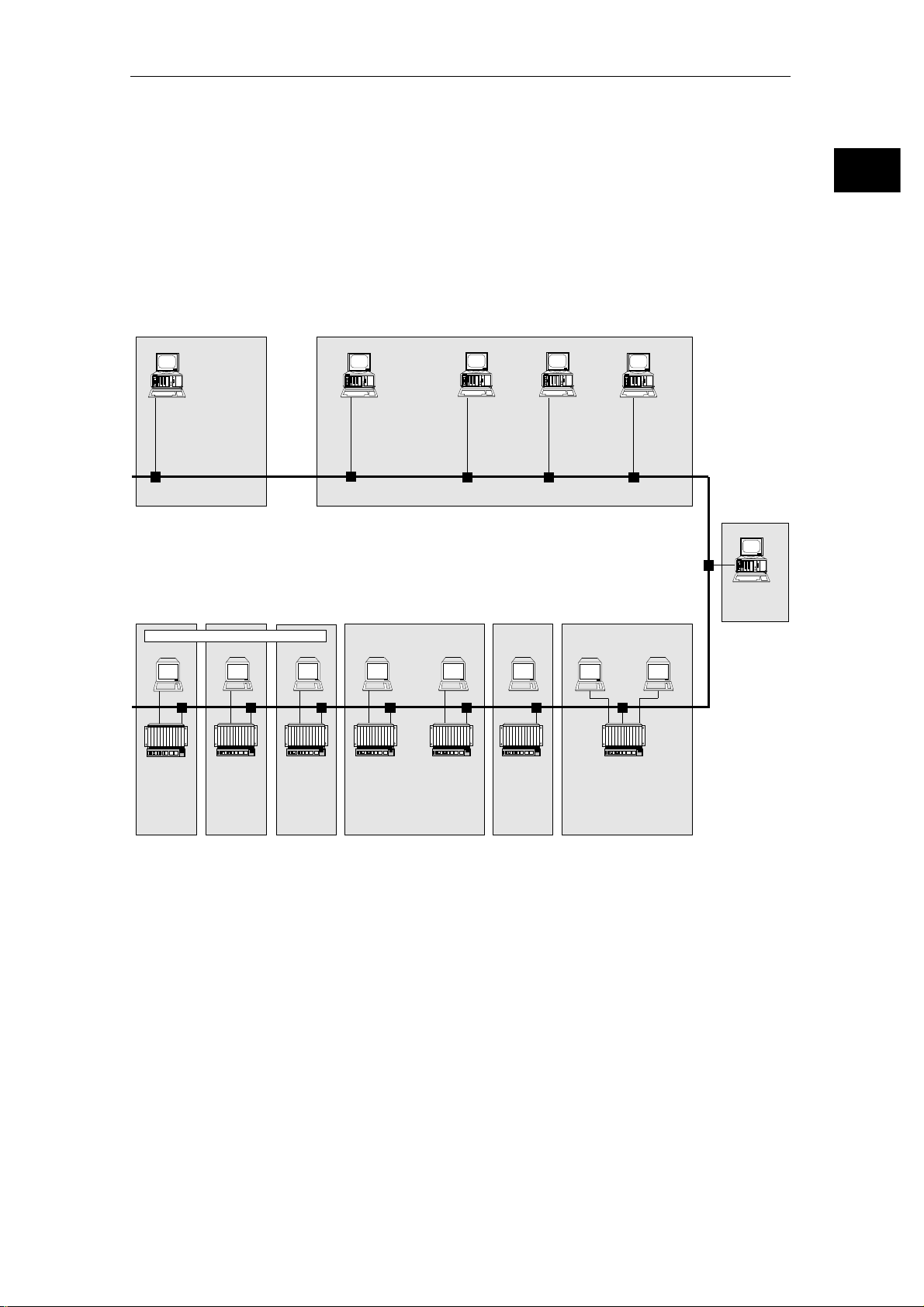
PG 770
System management Data base/
Service system
Control room
Fig. 1-1 illustrates the use of the S5-155 U progr am ma ble controller in
a cement w orks.
PG 770
logging
PG 770 PG 770
Quarry,
Raw meal silo,
Crusher,
Raw mill
Coal mill,
Kiln
PG 770
Cement
mills,
Dispatch
SINEC H1 bus
1
Process data control
Operation and monitoring (COROS)
S5-155U
Crusher,
Test station,
Limestone
store
S5-155U
Raw mill
Raw meal
silos
S5-155U S5-155U S5-155U S5-155U
Coal mill
Dryer
Heat
exchanger
Rotary
kiln
Clinker cooler
Clinker transport
Dust collector
Telephone
system
Central
control room
Fig. 1-1 Example of application of the S5-155U with the CPU 948
S5-155U
Cement mills
Distribution
PG 770
Process
data
editing
CPU 948 Programming Guide
C79000-D8576-C848-03
1 - 5
Page 20
.1
Typical Mode of Operation of a CPU
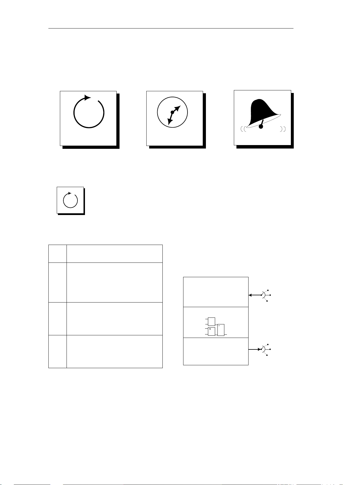
1.2 Typical Mode of Operation of a CPU
Mode of operation of a CPU
The following modes of operation are possib le in a CPU:
1. 2. 3.
Cyclic processing
Cyclic processing
This is the main part of all activities in the CPU. As the name alre ad y
says, the same operatio ns are re pe ate d in an endless cy cle .
Time-controlled processing
Interrupt-driven processing
Phase Sequence
All the input modules assigned to the
1
CPU are scanned by the system
program and the values read in are
stored in the proce ss imag e of the
inputs (PII).
The values contained in the PII are
2
processed by the user program and the
values to be output are entered in the
process image of the outpu ts ( PIQ) .
The values containe d in the proce s s
3
image of the outputs are output by the
system program to the output modules
assigned to the CPU.
Cyclic processing can be divided into thr ee main phases, as follows:
CPU
Read in process image
of the inputs
Evaluate input signals,
set output signals
&
I1.5
I1.6
I1.4
I1.3
Output process image
of the outputs
1
=
&
Q3.1
Process
Input I 1.3
Input I 1.4
Input I 1.5
Output Q 2.0
Output Q 3
Output Q 4.7
CPU 948 Programming Guide
1 - 6 C79000-D8576-C848-03
Page 21

Typical Mode of Operation of a CPU
Time-controlled processing
Interrupt-driven processing
Processing according to
priority
In addition to the cyclic processing, time- co ntr olle d processing is also
available for processes requiring control signals at constant intervals,
e.g. non-time critical mo nito rin g func tion s per fo rm ed every seco nd.
1
If the reaction to a particular process signal must be particularly fast, this
should be handled with interrupt-driven processing. With, for example,
a system interrupt, triggered via an interrupt generating module, you
can activate a special processing section within your program.
The types of processing listed above are handle d by the CPU
according to the ir prio rit y.
Since a fast reaction is required to a time or interrupt event, the CPU
interrupts cyclic processing to handle a time or interru pt ev ent. Cy clic
processing theref or e ha s the lowe st prio rity.
Whether or not the time-co ntr olle d proc essin g is mor e imp or tan t than
the interrupt controlled processing depends, among other things, on
the particular task . For this rea son, the priority of time and
interrupt-drive n proc essing on the CPU 948 can be selected.
CPU 948 Programming Guide
C79000-D8576-C848-03
1 - 7
Page 22
g
The Programs in a CPU
1.3 The Programs in a CPU
The program existing on every CPU is divided into the fo llowin g:
•• the system program
and
•• the user program.
System program
Update process image
of the inputs
Output process image
of the outputs
Manage memory
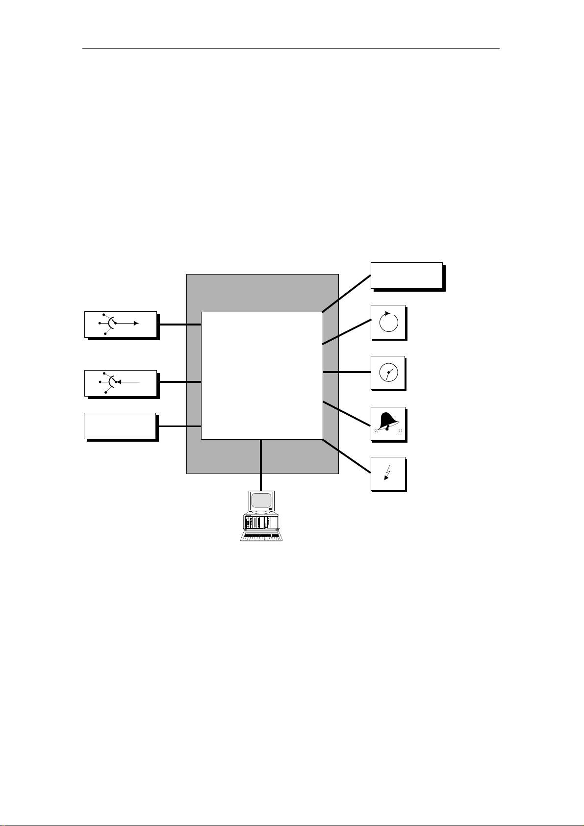
The system program organizes all the functions and sequences of the
CPU which do not involve a specific control task (refer to Fig. 1-2).
System
program
Communication with
the PG
Execute start-up
Call
user
processin
(interfaces)
Handle errors
Fig. 1-2 Tasks of the system program
1 - 8 C79000-D8576-C848-03
CPU 948 Programming Guide
Page 23

The Programs in a CPU
Tasks
User interfaces
The tasks include the follo wing :
1)
•• cold and warm restart,
•• updating the process image of the inp uts an d outpu tting the
process image of the outputs,
•• calling the cyclic, time- co ntr olle d an d inte rrup t-d riv en progr am s,
•• detection and handling of erro rs,
•• memory management,
•• communication with the programme r (PG) .
As the user, you can influenc e the rea ctio n of the CPU to partic ula r
situations and errors via spec ial inte rf ac es to the system progr am .
1
Storing the system program
System program defaults
Modifying the defaults
After switching on the power supp ly to the PLC (POWER UP) the
system program is read fro m the EP ROM to the internal operating
system RAM.
The following chapters, except for Chapter 7, describe the default
system reaction to process events or errors. Depending on the
defaults, the CPU changes to the stop mode if an oper atio n code err or
occurs and the error or ga niz atio n blo ck is not loaded .
You can modify the system resp onse by assign ing par am ete rs fo r the
data block DX 0.
Chapter 7 describes the system response following modification.
1)
When operating with several CPUs (multiprocessing) further tasks are involved.
CPU 948 Programming Guide
C79000-D8576-C848-03
1 - 9
Page 24

The Programs in a CPU
User program
Tasks
The user program contains all the functions required for processing a
specific control task . In gen er al ter ms, these functions can be
assigned to the interfac e pr ovided by the system program for the
various types of processing, as follows:
Type of processing Task
Cold and warm restart To provide the conditio ns un de r whic h
the other processing functions can start
from a defined status following a cold or
warm restart of the contro l system (e. g.
assigning specific values to signa ls).
Cyclic processing Constantly repeated signal processing
(e.g. logic operatio ns on binary signa ls,
reading in and analyzing analog values,
specifying binar y sign als fo r output,
outputting analog values).
Time-controlled proc essin g Special, time-dependent processing with
the following time conditions:
- faster than the average cycle,
- at a time interval greater than the
average cycle time,
- at a specified point in time.
Interrupt-driven proc essin g Special, fast reactions to certain proc ess
signals.
Error reaction Handling pr oblem s within the normal
sequence of the program.
CPU 948 Programming Guide
1 - 10 C79000-D8576-C848-03
Page 25
The Programs in a CPU
Structure
Organization
blocks
OB
STEP 5
operations
&
I1.5
I1.6
I1.4
&
I1.3
User memory
1
User program
Code blocks
Program
blocks
PB
STEP 5
operations
F 50.1
1
1
=
Q3.1
F 50.2
F 50.3
=
Q5.3
Function
blocks
FB/FX
STEP 5
operations
FB 8
SEGMENT 1
NAME :TRANS
0005 :L IB 3
0006 :T FW 200
0007 :C DB 5
0008 :DO FW 200
0009 :L DW 0
000A :T QW 6
000B :BE
Sequence
blocks
SB
STEP 5
operations
F1.7
S
I2.6
RQ
I1.3
Fig. 1-3 Structure of a STEP 5 user program
Storing the user program
Interfaces to the
system program
Data blocks
DB
static or dynamic data
(bits, bytes, words, double words)
DX
static or dynamic data
(bits, bytes, words, double words)
1: KH = 0101;
2: KF = +120;
3: KS = xy;
4: KY = 4.5;
5: KG =
6: KM =
7:
1: KH = FFFF;
2: KH = FFFF;
3: KH = FFFF;
4: KH = FFFF;
5: KH = FFFF;
6: KH = FFFF;
7:
After programming the user program, you must load it in the user
memory of the CPU 948 (directly fro m the PG) or via a memor y ca rd
whose contents are copied to the user memory by an OVERALL
RESET of the CPU.
Organization blocks are ava ilab le as inte rf ac es to the system program
for the special types of processin g.
CPU 948 Programming Guide
C79000-D8576-C848-03
1 - 11
Page 26

Which Operands are available to the User Program?
1.4 Which Operands are available to the User Program?
The CPU 948 provides the follo wing ope ra nd are as fo r pr ogramming:
•• process image and I/Os
•• flags (F flags and S flags)
•• timers/counters
•• data blocks
Process image of the inputs
and outputs PII/PIQ
Characteristics Size
I/O area (P area)
Extended I/O area (O area)
The user program can ac ce ss the fo llowin g da ta typ es
in the process image ex tre mely quickly:
- single bits,
- bytes,
- words,
- double words
Characteristics Size
The user program can ac ce ss the I/O mo dules dir ectly
via the S5 bus.
The following data types are po ssible :
- bytes,
- words.
Characteristics Size
128 bytes
each for
inputs and
outputs
256 bytes
each for
inputs and
outputs
The user program can ac ce ss the I/O mo dules dir ectly
via the S5 bus.
The following data types are po ssible :
- bytes,
- words.
CPU 948 Programming Guide
1 - 12 C79000-D8576-C848-03
256 bytes
each for
inputs and
outputs
Page 27

F flags
Which Operands are available to the User Program?
Characteristics Size
The flag area is a memory area which the user
program can access extremely quickly with certa in
operations.
The flag area should be used ideally for working data
required often.
The following data types can be accessed:
- single bits,
- bytes,
- words,
- double words.
Single flag bytes can be used as interpr ocesso r
communication flags (IPC flags) to exchange data
between the CPUs in the multiproce ssor mode (refer
to Chapter 10). IPC flags ar e up dated by the system
program at the end of the cycle via a buffer in the
coordinator or CP/IP.
2048 bits
1
S flags (extended flag area)
Characteristics Size
The CPU 948 also contains an addition al fla g ar ea , the
S flag area. The user program ca n also acc ess this ar ea
extremely quickly as with the F flags.
S flags cannot however by used as actual operands
with function block calls nor as IPC flags for data
exchange between the CPUs. The bit test oper atio ns of
the CPU 948 can also not be used with the S flags.
These flags can only be used with the PG system
software "S5-DOS" from version 3.0 upwards or
"S5-DOS/MT" from version 1.0 upwar ds.
32 768 bits
CPU 948 Programming Guide
C79000-D8576-C848-03
1 - 13
Page 28

Which Operands are available to the User Program?
Timers (T)
Characteristics Size
Counters (C)
Data words in the current data
block
The user program loads timer cells with a time value
between 10 ms and 9990 s and by means of a start
operation, decrements the timer from this value at the
preselected intervals until it reaches the value zero.
Characteristics Size
The user program loads co unter cells with a start value
(max. 999) and then increm en t s o r de crements th em.
Characteristics Size
256 timer
cells
256
counters
A data block contains constants and/or variables in the
byte, word or double word format. With STEP 5
operations, you can always access the "current" data
block (refer to Section 2.4.2).
The following data types can be accessed:
- single bits,
- bytes,
- words,
- double words.
1)
In data blocks with a length greater than 256 words, you can only access data
words with the numbers > 255 with operations for absolute memory access
(refer to Chapter 9).
256
words
1)
CPU 948 Programming Guide
1 - 14 C79000-D8576-C848-03
Page 29

How much Memory is available for the User Program?
1.5 How much Memory is available for the User Program?
For storing logic and data bloc ks, the CPU 948 only ha s the use r
memory in the internal RAM.
The CPU 948 is available with two versions of the user memory:
•• Version 1: with 640 Kbytes,
•• Version 2: with 1,664 Kbytes.
1
CPU 948 Programming Guide
C79000-D8576-C848-03
1 - 15
Page 30
How to Tackle Programming
1.6 How to Tackle Programming
If you are an experienced user, you have probably found the most
suitable method fo r cr ea ting programs for yourse lf an d you ca n skip
this section.
Less experienced reade rs will find tips for desig ning, program min g,
testing and starting up your STEP 5 program.
Implementation stages
Recursive procedure
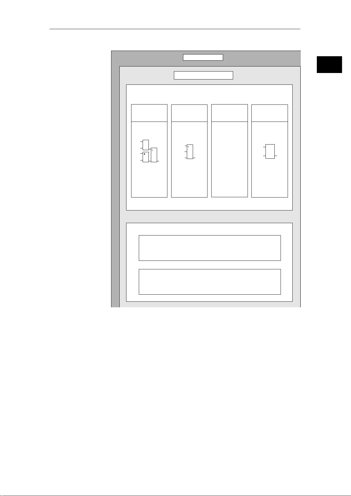
Stage 1
The implementa tion of the STEP 5 co ntr ol pr og ra m can be divided
into three stages:
Stage Activity
1 Determining the tec hn olo gic al task
2 Designing the program
3 Creating, testing and starting the program
In practice, you will recognize that certain steps must be repeate d
(recursive proced ur e) , e. g. when you rea lize that more signals are
required to improve the handling of the task.
Determining the tec hn olo gic al task :
Stage Activity
1 Create a general block diagram outlining the co ntr ol
tasks of your process.
2 Create a list of the input and output sign als re quired
for the task.
3 Improve the block diagram by assigning the signals
and any particular time conditio ns an d/or counter
statuses to the individual blocks.
CPU 948 Programming Guide
1 - 16 C79000-D8576-C848-03
Page 31

How to Tackle Programming
Stage 2
Designing the program
1
Stage Activity
1 Based on the improved bloc k dia gr am , decide on the
types of processing required of your program (cyclic
processing, time-contr olle d proc essin g etc.) and selec t
the OBs required for this.
2 Divide the types of processin g into tech no log ica l
and/or functional units.
3 Check whether the units can be assign ed to a progr am
or function block and select the blocks you requir e
(PB x, FB y etc.)
4 Find out which timers, counters an d da ta or resu l ts
memory you require.
5 Specify the tasks for each of the propo sed logic bloc ks
and the data for flags and data bloc ks whic h ma y be
required. Create flow dia gr am s for the log ic blocks.
Notes on the scope of
cyclic processing
When deciding on the types of proc essin g, kee p the follo wing
conditions in mind:
•• The cycle must run through quickly enough. The process statuses
must not change more quickly than the CPU can rea ct. Other wise
the process can get out of control.
•• The maximum reaction time should be taken as twice the cyc le
time.
The cycle time is determined by the cy clic proce ssing of the
system program and the type and scope of the use r progra m. It is
often not constant, since the cyclic user program may be
interrupted when time and inte rr upt-driven program sectio ns ar e
called.
CPU 948 Programming Guide
C79000-D8576-C848-03
1 - 17
Page 32

How to Tackle Programming
Stage 3
Creating, testing and startin g up the pr ogram:
Stage Activity
1 Decide on the type of repr ese ntation for the logic
blocks (LAD, CSF or STL, refer to Chapter 2).
Remember that function blocks can only be cre ate d in
the STL method of represen tation.
2 Program all logic and data bloc ks (p lea se re fe r to yo ur
STEP 5 manual).
3 Start up the blocks one after the other (you may have
to program a differe nt OB fo r ea ch indiv idu al step, to
call the logic blocks):
1a: load the block(s)
1b: test the block(s)
(For more detailed info rmation please refer to your
STEP 5 manual and Chapter 11).
4 When you are certain that all the logic bloc ks ru n
correctly and all the data can be correc tly ca lculated
and stored, you can start up your whole progr am .
Note on test strategies
When you actually start up your progr am for the fir st tim e in genu ine
process operation, i.e. with real input an d more impo rta ntly output
signals, is a decision that must be left up to yourself or to a team of
experts.
The more complex the proc ess, the gr ea ter the risk and ther ef ore the
greater the care re qu ire d whe n starting up.
CPU 948 Programming Guide
1 - 18 C79000-D8576-C848-03
Page 33

1.7 Programming Tools
Programming Tools
Suitable PGs
Suitable software
The following program me rs ar e av aila ble for creating your user
program, PG 685, PG 710, PG 730, PG 750 and PG 770. You can
check on the performance and cha ra cte ristic s of the se devic es in the
catalog ST 59 /9/.
Note
If you wish to use the full range of performa nce of the CPU 948
in your automation softwar e, (pa rtic ula rly the DX 0 screen, the
"Output ISTACK" screen, the displa y with the "memor y
configuration" func tion and the PG functions via the backplane
bus) you require the PG system sof twar e "STEP 5/ST" from
version 6.3 upwards or "STEP 5/MT" from version 6.0 upwards
plus the "Delta diskette CPU 948" and a PG 7xx.
You can crea t e user programs for SIMATIC S5 programmable
controllers as follows:
•• In the STEP 5 programming language,
Here you require the STE P 5 pro gramming package alo ng with the
system software STEP 5/ST or STEP 5/MT (descr iptio n, refer to
/3/ in Further Reading ),
1
or
•• In a higher programming language :
If you are familiar with programming in higher programming
languages, you can also formulate your STEP 5 program for the
CPU 948 as follows:
- SCL (refer to /12/ in Furth er Rea din g, the S CL com pile r i s
contained in the PG software "S5-DOS/MT" from version 6
upwards.)
or
- C with S5 C compiler (refer to /13/ in Further Reading).
You can also create programs for sequence control systems in a
graphic representation using the GRAPH 5 programming package
(description, refer to /4/ in Further Reading).
Depending on the task, you can also inc or porate "off-the-peg"
standard function bloc ks in yo ur user progr am . Th e pe rf or ma nce and
characteristics of the se blocks are described in the ca talog ST 57 /11/.
CPU 948 Programming Guide
C79000-D8576-C848-03
1 - 19
Page 34

What is New with the CPU 948?
1.8 What is New with the CPU 948?
1.8.1
CPU 948, Version A01 Compared with the CPU 946/947, the CPU 948 versio n A01 has new
characteristics and functions an d signific an t improvem ents in
performance.
Faster processing
Larger user memory
Memory Card
The CPU 948 is between three and five times fa ster than the CPU
946/947. The exact execution times can be found in your Pocket
Guide /1/.
CPU 948
only RAM (integrated)
640 Kbytes or 1664 Kbytes in
internal RAM integrated in the
CPU 948, for logic and data
blocks.
RAM or EPROM cartridges
Max. 896 Kbytes, of which 128
Kbytes fixed as RAM plus
additional 6 RAM or EPROM
cartridges, each with 128 Kbyte s
in 355 memory modules.
CPU 946/947
CPU 948 CPU 946/947
SIMATIC Memory Card (Flash
EPROM), 256 Kbytes to
2 Mbytes;
the memory card is programmed
on the PG and its contents loaded
in the user memory (inte rnal
RAM) following an OVERALL
RESET.
1 - 20 C79000-D8576-C848-03
SIMATIC memory c ar tridges
RAM or EPROM, max. 128
Kbytes;
data blocks can be copied to the
DB RAM from EPROM
(OB 254/255).
CPU 948 Programming Guide
Page 35

What is New with the CPU 948?
Interruptability at block or
operation boundaries
Expansion of
time-controlled program
processing
With a CPU 948, there is no longer a distinctio n betwee n 150/155U
modes. This means the following chan ge s compa re d with the CPU
946/947:
CPU 948 CPU 946/947
- Processing system interrupts:
possible with interrupts at the
operation or block boundaries
- Multiprocessor mode:
interrupts possible at the
operation or block boundaries.
Apart from the familiar cyclic time d inte rrup ts at fixe d interv als, the
following new interrupts are also proc esse d:
•• delayed interrupt (OB 6),
•• clock-controlle d inte rr up t (OB 9).
Both interrupts are only possible when "process interrupts via IB 0 =
off" is set in DX 0.
- Processing systems interrupts:
only possible with interrupts
at operation boundarie s.
- Multiprocessor mode:
only possible with interrupts
at operation boundarie s.
1
Expansion of PG
communication
New special functions
•• Second PG serial interfac e via plug -in PG submo dule.
•• PG functions via SINEC H1 and para llel ba ck pla ne bus.
•• Delete ACCU 1 to ACCU 4 (OB 131)
Roll-up ACCU (OB 132)
Roll-down ACCU (OB 133)
•• Enable/disable "bloc k sing le time d interr upts" ( OB 141)
Enable/disable "delay all inter rupts" (OB 142 )
Enable/disable "delay single timed interrupts" (OB 143)
•• Read/set system time, compatible with CPU 928B (OB 150),
•• Assign parameters for cloc k- co ntr olle d inte rr upt ( OB 9), (OB 151 )
•• Assign parameters for dela yed inte rr upt (OB 6), (OB 153)
•• Restart cycle monitoring time (OB 222)
CPU 948 Programming Guide
C79000-D8576-C848-03
1 - 21
Page 36

What is New with the CPU 948?
Self test functions
OB 0
WHAT IS TESTED? WHEN?
The user memory In OVERALL RESET
The BASP signal
In STOP
(disable command output)
The hardware clock In COLD RESTART
The cycle time monitorin g In START-UP
The address lines Cyclically in RUN
The code of the system program
Cyclically in RUN
(checksum )
The code of the STEP 5 logic
Cyclically in RUN
blocks in the user memory
(checksum)
The test functions can be activ ated individually, they are per fo rmed in
"time slices".
New HDBs for the CPU 948
CPU 948 CPU 946/947
With the PG functions,
BSTACK, ISTACK and DIR,
only the operating syste m
organization block OB 0 is
displayed.
With the PG functions,
BSTACK, ISTACK and DIR, all
the operating system
organization bloc ks > OB 40 are
displayed.
"New" handling block s (HDBs) are req uir ed for the CPU 948. T he
HDBs of the CPU 946/947 cannot be used in the CPU 948.
The HDBs for the CPU 948 are those for the S5-135U (CPU 922,
CPU 928, CPU 928B), and can be obtained under the following order
numbers:
6ES5 842-xCB01 ("HDBs for the CPU 922, 928, 928B and CPU 948")
where:
x = 8 stands for the operating system S5-DOS (PCP/M)
x = 7 stands for the operating system MS-DOS, S5/DOS-MT.
CPU 948 Programming Guide
1 - 22 C79000-D8576-C848-03
Page 37

1.8.2 CPU 948, Version A02
What is New with the CPU 948?
The CPU 948, version A02, provide s you with new fe atu re s and
functions compared with the CPU 948, version A01:
1
Communication via the
second serial interface
Software protection
New special function OBs
As with the CPU 928B, the following communication s optio ns ar e
available via the second ser ial inte rf ac e:
•• RK 512,
•• data transmission with procedure 3964/3964R,
•• open drivers,
•• SINEC L1.
For more detailed info rmation, see the communicatio ns manual
(Further Reading /14/).
You can protect your user progr am from re ad and write access using a
password (see Chapter 8, RS 120).
The following special func tion OBs are availab le (see Chapter 6):
•• OB 129: Battery state
•• OB 181: Test data blocks DB/DX
1.8.3 CPU 948, Version A03 and Higher
•• OB 182: Copy data areas
Special function OB 180: Variable data block access.
CPU 948 Programming Guide
C79000-D8576-C848-03
1 - 23
Page 38

Converting User Programs of the CPU 928B for the CPU 948
1.9 Converting User Programs of the CPU 928B for the CPU 948
The following section inf or ms you ab out the po ints you sho uld
remember when you convert user programs written for the CPU 928B
for use on the CPU 948.
Operations
Operations CPU 928B CPU 948
IA/RA (disable/enable
interrupts)
LIR/TIR 16 bit long addresses are used. 20 bit long addresses are used .
Block transfer operation TNB
Block transfer operation TNW
All process interrupts are disa ble d or
enabled
16 bit long addresses are used. The operation does not exist.
- 16 bit long addresses are used.
- Block transfer s from the 8-bit to the
In the following opera tion s, no te the diff erences in the exec utio n an d
handling (among other things the different mem ory utiliz atio n) .
Only the process interru pts via inpu t
byte IB 0 are disabled or enabled.
Instead of these operations, use the
special function OBs OB 122 or
OB 142.
Adaptation is necessary.
Use TNW for block transfer from the
8-bit to the 8-bit area.
- 20 bit long addresses are used.
Adaptation is necessary.
- only block transfers from the
8-bit area and vice versa are
possible.
8-bit to the 8-bit area and from the
16-bit to the 16-bit areas possible
with TNW.
- for the block tra nsf er from
the 8-bit to the 16-bit area use
the operation TXB,
- for the block tra nsf er from
the 16-bit to the 8-bit area use
the operation TXW.
(TXB and TXW do not exist on
a CPU 928B)
All operations with the
BR register
1 - 24 C79000-D8576-C848-03
The BR register is 20 bits wide. The BR register is 32 bits wide.
Adaptation is necessary.
CPU 948 Programming Guide
Page 39

Timer processing
FB 0 as cycle block
Converting User Programs of the CPU 928B for the CPU 948
CPU 928B CPU 948
The timers are updated during
start-up.
CPU 928B CPU 948
The timers are only updated in
the RUN mode
(Reason: compatibility with
CPU 946/947)
1
Default priorities
Data block DB 0
(block address list)
If no cycle block OB 1 exists, the
system program calls FB 0
cyclically, provided it is loaded.
CPU 928B CPU 948
Process interrupts have higher
priority than timed interrupts.
CPU 928B CPU 948
The block address list contains
the direct start addresses of the
blocks.
Only OB 1 can be used for cyclic
processing. If you have
programmed FB 0, create an
OB 1 in which FB 0 is called.
Timed interrupts have pr ior ity
over process interrupts via IB 0
or system interrupts. You can
change the priority with the
parameters in DX 0.
The block address list contains
the segment addresses of the
blocks. To obtain the start
address of a block, its segment
address must be shifted 4 bits to
the left.
CPU 948 Programming Guide
C79000-D8576-C848-03
1 - 25
Page 40

Converting User Programs of the CPU 928B for the CPU 948
Data block DX 0
Using the RT area
Organization blocks
Error OBs
You must create a new DX 0 data block (see Chapter 7), since the
DX 0 for the CPU 928B has a different structure and settings.
With the CPU 928B, the RT area is not used by the system program,
with the CPU 948 it is used to some extent by the handlin g blo ck s.
You can only use the RT area for your user program when you do not
use any standard FBs and any PG functions via SINEC H1 and the S5
bus.
The number and function of the error and spec ial fu nction OBs are not
the same on the CPU 928B and CPU 948:
The following error OBs of the CPU 948 respond differently from
their namesakes on the CPU 928B:
OB Function Error IDs
OB 19
OB 26
Same as on
CPU 928
Different fr om
CPU 928B
OB 27
OB 28
OB 29
OB 30
Function different
from that on
CPU 928B
–
OB 31
Special function OBs
OB Note
OB 110
OB 152
OB 160 to 16 3
OB 170
OB 190 to 19 3
OB 216 to 21 8
These OBs do not exist on the CPU 948
OB 220 and 221
OB 224
OB 226 to 22 8
OB 240 to 24 2
OB 250 and 251
On the CPU 948, the OB is replaced by :
OB 111
OB 112
OB 113
OB 120
OB 121
OB 122
OB 123
OB 131
OB 132
OB 133
OB 122
OB 141
OB 142
OB 143
OB 122 Param ete r assig nm ent is dif fe rent fr om that of the
CPU 928B OB 122
(reason: compatibility with CPU 946/947).
CPU 948 Programming Guide
1 - 26 C79000-D8576-C848-03
Page 41

Converting User Programs of the CPU 928B for the CPU 948
OB Note
R64 controller software
Standard FBs
OB 180 In contra st to the CPU 928B, the acc ess wind ow of
the CPU 948 can only be shifted by a multiple of
16.
OB 200
OB 202 to 20 5
(multiprocessor
communication)
The R64 controller softwa re can not be ru n on the CPU 948.
Generally, the stan da rd fun ctio n blo ck s used on the CPU 928B (e.g.
for IPs) must be replaced by those for the CPU 948. The HDBs are an
exception these can be tak en from the CPU 928B (se e Sec tion 1.8 .1 ).
In contrast to the CPU 928B, these CPU 948 OBs
change the content of ACCU 4.
1
CPU 948 Programming Guide
C79000-D8576-C848-03
1 - 27
Page 42

User Program
2
Contents of Chapter 2
2.1 STEP 5 P rogrammi ng Language . . . . . . . . . . . . . . . . . . . . . . . . . . . . . . . . . . . . . . . . . . . 2 - 4
2.1.1 The LAD, CSF, STL Methods of Representation . . . . . . . . . . . . . . . . . . . . . . . . . . . . . . 2 - 4
2.1.2 Structured Programming. . . . . . . . . . . . . . . . . . . . . . . . . . . . . . . . . . . . . . . . . . . . . . . . . . 2 - 5
2.1.3 STEP 5 Operations . . . . . . . . . . . . . . . . . . . . . . . . . . . . . . . . . . . . . . . . . . . . . . . . . . . . . . 2 - 6
2.1.4 Number Representation . . . . . . . . . . . . . . . . . . . . . . . . . . . . . . . . . . . . . . . . . . . . . . . . . . 2 - 8
2.1.5 STEP 5 Blocks and Stor ing them in Memory. . . . . . . . . . . . . . . . . . . . . . . . . . . . . . . . 2 - 12
2.2 Program, Organization and Sequence Blocks . . . . . . . . . . . . . . . . . . . . . . . . . . . . . . . . 2 - 16
2.2.1 Organization Blocks as User Interfaces. . . . . . . . . . . . . . . . . . . . . . . . . . . . . . . . . . . . . 2 - 18
2.2.2 Organization Blocks for Special Functions . . . . . . . . . . . . . . . . . . . . . . . . . . . . . . . . . . 2 - 22
2.3 Function Blocks . . . . . . . . . . . . . . . . . . . . . . . . . . . . . . . . . . . . . . . . . . . . . . . . . . . . . . . 2 - 23
2.3.1 Structure of Function Blocks . . . . . . . . . . . . . . . . . . . . . . . . . . . . . . . . . . . . . . . . . . . . . 2 - 24
2.3.2 Programming Function Blocks. . . . . . . . . . . . . . . . . . . . . . . . . . . . . . . . . . . . . . . . . . . . 2 - 26
2.3.3 Calling Function Blocks and Assigning Parameters to them . . . . . . . . . . . . . . . . . . . . 2 - 28
2.3.4 Special Function Blocks. . . . . . . . . . . . . . . . . . . . . . . . . . . . . . . . . . . . . . . . . . . . . . . . . 2 - 33
2.4 Data Blocks. . . . . . . . . . . . . . . . . . . . . . . . . . . . . . . . . . . . . . . . . . . . . . . . . . . . . . . . . . . 2 - 35
2.4.1 Creating Data Blocks . . . . . . . . . . . . . . . . . . . . . . . . . . . . . . . . . . . . . . . . . . . . . . . . . . . 2 - 37
2.4.2 Opening Dat a Blocks . . . . . . . . . . . . . . . . . . . . . . . . . . . . . . . . . . . . . . . . . . . . . . . . . . . 2 - 38
2.4.3 Special Data Blocks . . . . . . . . . . . . . . . . . . . . . . . . . . . . . . . . . . . . . . . . . . . . . . . . . . . . 2 - 41
CPU 948 Programming Guide
C79000-B8576-C848-03
2 - 1
Page 43

2User Program
The following cha pte r ex plains the component s tha t mak e up a
STEP 5 user program for the CPU 948 and how it can be structu re d.
2
CPU 948 Programming Guide
C79000-B8576-C848-03
2 - 3
Page 44

STEP 5 Programming Language
2.1 STEP 5 Programming Language
With the STEP 5 programming language, you convert automation
tasks into programs that run on SIMATIC S5 programmable
controllers. You can program simple binary functions, complex
digital functions and arithmetic operations including floating
point arithmetic using STEP 5.
Types of operation
The operations of the STEP 5 programming langua ge are divided into
the following groups:
Basic operations
•• you can use these operations in all logic blocks
•• methods of representation: ladder diagra m (L AD), control system
flowchart (CSF), statement list (STL).
Supplementary operation s and system ope rations:
•• can only be used in function blocks
2.1.1 The LAD, CSF, STL Methods of Representation
Graphic representation or
list of statements
•• only statement list (STL) method of repr esen tatio n
•• system operations: only experienced STEP 5 programmer s shou ld
use system operations
When programming in STEP 5, you can choose between the three
methods of representation ladder diagram (LAD), control system
flowchart (CSF) and statement list (STL) for each individual logic block.
You can choose the method of representation that best suits your
particular application.
The machine code MC5 that the pr ogra mm ers (PGs) generate is the
same for all three meth od s of rep re se ntation.
If you follow certain rules when pro gram min g in STE P 5 (see /3/) , the
programmer ca n tra nslate your user pro gr am from on e me tho d of
representa tion into any other.
While the ladder diagram (LAD) and contro l system flowc hart (CSF)
methods of representa tion represent your STEP 5 progra m
graphically, statement list (STL) repre se nts STEP 5 oper atio ns
individually as mnemonic abbreviations.
CPU 948 Programming Guide
2 - 4 C79000-B8576-C848-03
Page 45

STEP 5 Programming Language
Ladder diagram
Programming with
graphic symbols
like a circuit diagram
Statement list
Programming with
mnemonic abbreviations
of function designations
Control system flowchart
Programming with
graphic symbols
complies with complies with complies with
DIN 19239 DIN 19239
IEC 117-15
DIN 40700
DIN 40719
DIN 19239
STL CSFLAD
A
AN
A
ON
O
=
I
I
I
I
I
Q
&
2
> = 1
Fig. 2-1 Methods of representation in the STEP 5 programming language
Graphic representation of
sequential controls
2.1.2 Structured Programming Using STEP 5, you can structure your program by dividing it into
GRAPH 5 /4/ is a programming language for graphic representation of
sequential controls. It is at a higher level than the LAD, CSF, STL
methods of representation. A program written in GRAPH 5 as a
graphic representation is automatically conve rte d to a STE P 5
program by the PG.
self-contained program sections (blocks). This division of your
program clarifies the essen tial pr ogram structures making it easy to
recognize the system parts that are related within the software.
CPU 948 Programming Guide
C79000-B8576-C848-03
2 - 5
Page 46

STEP 5 Programming Language
Structured programming offers you the following advantages:
•• simple and clear creatio n of progr am s, even lar ge ones
•• standardization of progra m parts
•• simple program organiz atio n
•• easy program change s
•• simple, section by section program test
•• simple system start-up
What is a block?
2.1.3 STEP 5 Operations A STEP 5 operation is the smallest independent unit of the user program.
A block is a part of the user program that is distinguished by its
function, structure or applic atio n. You ca n dif fe re ntia te be twee n
blocks that contain statements (co de ) i.e . or ga niz atio n blo ck s,
program blocks, function blocks or sequen ce bloc ks, and blocks that
contain data (data block s) .
It is the work specification for the CPU. A STEP 5 operation consists of
an operation and an operand as shown in the following example:
Example
Operation code
Parameter
:O F 54.1
Operation
(what is to be done?)
Operand
(with what is the
operation to be done?)
CPU 948 Programming Guide
2 - 6 C79000-B8576-C848-03
Page 47

STEP 5 Programming Language
Absolute and symbolic
operands
Application of STEP 5
operations
You can enter the operand absolutely or symbolically (using an
assignment list) as shown in the following example :
Absolute representation: :A I 1.4
Symbolic representation: :A -Motor1
For more informatio n on absolu te an d symb olic progr am ming, refer to
your STEP 5 manual.
The STEP 5 operation set enables you to do the following:
•• set or reset and combine binary values logically
•• load and transfer values
•• compare values and process them arithmetically
•• specify timer and counter valu es
•• convert number repre se ntations
•• call blocks and execute jumps within a block
and
2
Result of logic operation RLO
•• influence program execution
The central bit for contro lling the program is the result of logic
operation RLO. This is obtained as a result of binary logic operations
and is influenced by some operations.
Section 3.5 describes the whole STEP 5 operation set and explains how
the RLO is obtained. This section also includes programming examples
for individual STEP 5 operations.
CPU 948 Programming Guide
C79000-B8576-C848-03
2 - 7
Page 48

STEP 5 Programming Language
2.1.4 Number Representation To allow the CPU to log ica lly co mbine, modify or compare numer ica l
values, these values must be loc ate d in the acc um ula tors (working
registers of the CPU) as binary numbers.
Depending on the operations to be carried out, the following number
representations are permitted in STEP 5:
Binary numbers: 16-bit fixed point numbers
32-bit fixed point numbers
32-bit floating point numbe rs (with a 24-b it
mantissa)
Decimal numbers: BCD-coded numbers (sign and 3 digits)
Numerical input on the PG
Permitted operations
When you use a programmer to input or displa y numb er valu es, you
set the data format on the program mer (e .g . KF or fix ed poin t) in
which you intend to enter or display the valu es. Th e prog ra mm er
converts the internal re presentation into the form you have requ ested .
You can carry out all arithmetic operations with the 16-bit fixed
point numbers and floating point numbers, including comparison,
addition, subtrac tion , multiplication and division.
Note
Do not use BCD-coded numbers for arithmetical operations, since
this leads to incorrect results.
Use 32-bit fixed point numbers to execute comparison opera tion s.
These are also necessary as an intermediate level when converting
numbers in BCD code to floating point numbers. With the operations
+D and -D they can also be used for addition and subtraction.
The STEP 5 programming language also has conversion operations that
enable you to convert numbers directly to the most important of the other
numerical representations.
CPU 948 Programming Guide
2 - 8 C79000-B8576-C848-03
Page 49

STEP 5 Programming Language
16-bit and 32-bit fixed
point numbers
Coding of fixed point numbers
PG input
Permitted numerical range
Fixed point numbers are whole binary numbers with a sign.
Fixed point numbers are 16 bit (= 1 word) or 32 bit (= 2 words) in
binary representation. Bit 15 or bit 31 contains the sign.
•• ’0’ = positive numb er
•• ’1’ = negative numbe r
The two’s complement re pr esentation is used for negative numbers.
Input of 16-bit fixed point num ber da ta fo rmat at the PG:KF
Input of 32-bit fixed point num ber da ta fo rmat at the PG:DH
16-bit fixed point num be r
-32768 to +32767 (16 bits)
32-bit fixed point num be r
-2147483648 to +2147483647 (32 bits)
(8000 0000H to 7FFF FFFFH)
2
Using fixed point numbers
Floating point numbers
Use fixed point numbers for simple ca lcu lations and for comparing
number values. Since fixe d point numb er s ar e always whole numbers,
remember that the result of dividing two fixed poin t num be rs is also a
fixed point number without dec ima l places.
Floating point numbers ar e positiv e an d nega tive fra ctio ns. Th ey
always occupy a double word (32 bits). A floating point number is
represented as an exponential number. The mantissa is 24 bits long
and the exponent is 8 bits long.
In the CPU 948, the default mantissa is 24 bits long (bits 0 to 23) for
adding, subtrac ting, multiplying and dividing.
The exponent indicates the order of magnitude of the floating point
number. The sign of the exponent tells you whether the value of the
floating point number is greater or less than 0.1.
CPU 948 Programming Guide
C79000-B8576-C848-03
2 - 9
Page 50

STEP 5 Programming Language
Using floating point numbers
Accuracy
Coding floating point numbers
Use floating point numbers for solvin g ex ten siv e ca lcu latio ns,
especially for multiplica tion and division or whe n you ar e wor kin g
with very large or very small numbers!
The mantissa indicates the accu ra cy of the floa ting poin t numbe r as
follows:
•• Accuracy with a 24-bit mantissa:
-24
= 0.0000 00059604 (corresponds to 7 decimal places)
2
If the sign of the mantissa is "0" the number is positive; if the sign is
"1" it is a negative number in its two’ s comp lem en t rep re se nta tion.
The floating point value ’0’ is represented as the bina ry value
80000000H (32 bits, see below).
Coding a floating point number:
31 30 24 23 22 0
V26 ... . ... 20V2-1 .... . . . . . ... 2
-23
Exponent Mantissa
Specification of the da ta fo rmat fo r flo atin g point nu mber s at the
PG: KG
Permissible numerical range
Input/output on PG
± 0.1469 368 x 10
-38
to ± 0.1701412 x 10
39
a) in a logic block:
You want to load the number N = 12.345 67 as a flo atin g point
number.
Input:
:LKG1234567+2
CPU 948 Programming Guide
2 - 10 C79000-B8576-C848-03
Page 51

STEP 5 Programming Language
b) in a data block:
PG display after you enter the line:
:L KG + 1234567 + 02
Mantissa with sign Exponent (base 10)
with sign
Value of the number input: +0.1234567 x 10
You want to define the numb er N = - 0.00 5 as a floating point
constant.
Input:
6: KG = - 5 - 2
PG display after you enter the line:
+2
2
= 12.345 67
Numbers in BCD code
6: KG =- 500000 0 - 02
Mantissa with sign Exponent (base 10)
with sign
-2
Value of the number input : - 0.5 x 10
Decimal numbers ar e re pr esen ted as numb er s in BCD code. With the ir
sign and three digi t s, th ey occ up y 16 bit s (1 word ) in an accumulator
as shown in the following example:
15 12 11 8 7 4 3 0
V V V V hundreds tens ones
The individual digits are positive 4-bit binary numbers between 0000 and
1001 (0 and 9 decimal).
The left bits are reserved for the sign as follows:
Sign for a positive number: 0000
Sign for a negative number: 1111
= 0.005
Permissible numerical range
CPU 948 Programming Guide
C79000-B8576-C848-03
-999 to +999
2 - 11
Page 52

STEP 5 Programming Language
2.1.5 STEP 5 Blocks and Storing them in Memory
Identification
Block types
Organization blocks (OB)
A block is identified as follows:
•• the block type (OB, PB, SB, FB, FX, DB, DX)
and
•• the block numbe r (n umbe r be twee n 0 an d 255) .
The STEP 5 programming language diff er en tiate s betwee n the
following block types:
Organization blo ck s ar e the inter face between the syste m prog ra m an d
the user program. Th ey can be div ided into two groups as follows:
With OB 1 to OB 39, you can control program execution, the restart
procedure of the CPU and the reaction in the event of an err or . You
program these blocks your self according to your automation task.
These OBs are called by the system program.
OBs 40 to 100 are blocks belonging to the operating system. You
must not call these blocks.
OBs 121 to 255 contain special function s of the syste m prog ra m. You
can call these blocks, if re quire d, in your user progr am .
Program blocks (PB)
Sequence blocks (SB)
You require program blocks to structure your program. They contain
program parts divided according to technological and functional
criteria. Progr am bloc ks rep re se nt the heart of the user program .
Sequence blocks were orig ina lly spec ial pr og ra m blo cks fo r step by
step processing of sequen ce rs. In the me an time, however, sequen cers
can be programmed with GRAPH 5/4/. Sequence blocks have
therefore lost their original significance in STEP 5.
Sequence blocks now represent an extensio n of the pr og ra m blo ck s
and are used as program blocks.
CPU 948 Programming Guide
2 - 12 C79000-B8576-C848-03
Page 53

STEP 5 Programming Language
Function blocks (FB/FX)
Data blocks (DB/DX)
Formal structure
of the blocks
Block header
You use function blocks to progr am fre qu en tly re cu rr ing and/or
complex functions (e .g . dig ital fu nctions, sequence control syste ms,
closed loop controls and signalling functions).
A function block can be calle d seve ra l tim es by hig he r or de r blo ck s
and supplied with new operands (a ssign ed par am ete rs) at ea ch call.
Using block type FX doubles the maximum number of possible function
blocks.
Data blocks contain the (fix ed or varia ble ) da ta with whic h the user
program works. This type of block con tain s no STEP 5 sta tem en t s and
has a distinctly differ en t function from the other blocks. U sin g blo ck
type DX doubles the number of possible data bloc ks.
All blocks consist of the following two parts:
•• a block header
and
•• a block body
The block header is always 5 words long and contains information for
block management in the PG and data for the system program.
2
Block body
Depending on the block type, the block body conta ins the fo llowin g:
•• STEP-5 operations (in OB, PB, SB, FB, FX),
•• variable or constant data (in DB, DX)
and
•• a formal operand list (in FB, FX).
CPU 948 Programming Guide
C79000-B8576-C848-03
2 - 13
Page 54

STEP 5 Programming Language
Block preheader
Maximum length
Available blocks
The programmer also genera tes a block preheader (DV, DXV, FV,
FXV) for block types DB, DX, FB and FX. These block pre head er s
contain information about the da ta form at (for DB and DX) or the
jump labels (for FB and FX). Only the PG c an evaluate this
information. Consequ ently the block preheaders are not transferred to
the CPU memory. You canno t influence the conte nts of the bloc k
header directly.
A STEP-5 block can oc cu py a max imum of 32 767 words in the
program memory of the CPU (1 word corre sp onds to 16 bits).
You can program the follo wing bloc k typ es:
OB 1 to 39
FB 0 to 255
total 512
FX 0 to 255
PB 0 to 255
SB 0 to 255
DB 2 to 255
total 508
DX 3 to 255
Data blocks DB 0, DB 1, DB 2, DX 0, DX 1 and DX 2 contain
parameters. These are reserved for specific functions and you cannot use
them as normal data blocks.
Data block DX 2 is reserved for the 2nd serial interface and you should
not use it.
CPU 948 Programming Guide
2 - 14 C79000-B8576-C848-03
Page 55

STEP 5 Programming Language
Block storage
The programme r store s all pr og ra mm ed bloc ks in the pr og ram
memory in the order in which they are transf er red (Fig. 2-2). With the
PG function "transfe r data blocks A" the logic bloc ks are transferred
first followed by the data blocks.
The start addresses of all stored blocks are place d in an addre ss list in
data block DB 0.
Address 0
PB1
FB1
PB2
DB1
SB10
Location of blocks
in the user memory
2
Correcting and
deleting blocks
OB1
Fig. 2-2 Example of block storage in the user memory
When you co rr ec t blocks, the old block is declared invalid in the
memory and a ne w b loc k i s en tered.
Similarly, when blocks are deleted, they are not really deleted, instead
they are declared invalid. The space they occupy is, however, not
released and is not available for blocks loaded later.
Note
You can use the COMPRESS MEMORY online function to make
space for new blocks. This function optimiz es the utiliz atio n of
the memory by deletin g blo ck s ma rk ed as inv alid and shifting
valid blocks together.
CPU 948 Programming Guide
C79000-B8576-C848-03
2 - 15
Page 56

Program, Organization and Sequence Blocks
2.2 Program, Organization and Sequence Blocks
Program blocks (PBs), organization blocks (OBs) and sequence
blocks (SBs) are the same with re spec t to pro gram min g an d calling.
You can program all three type s in the LAD, CSF an d STL meth od s
of representation.
Programming
When programming organization, pr og ram and sequence bloc ks,
proceed as follows:
Step Action
1 First indicate the type of block and then the number of the
block that you want to program.
The following numbers ar e av ailable for the type of
block listed:
- program blo ck s 0 to 255
- sequence blocks 0 to 255
- organization block s 1 to 39
2 Enter your program in the STEP 5 programming language.
When programming PBs, OBs and SBs, you can only
use the STEP 5 basic operations!
A STEP 5 block should always be a self-c ontained
program section.
Logic operations must always be complete d
within a block.
3 Complete your program input with the block end
operation "BE".
Block calls
2 - 16 C79000-B8576-C848-03
With the exception of OB 1 to OB 39 you must call the blocks to
process them. Use the special STE P 5 bloc k ca ll ope ra tion s to ca ll the
blocks.
You can program blo ck calls insid e an organ iza tion, program,
function or sequenc e blo ck . Th ey can be comp ar ed with jump s to a
subroutine. Each jum p ca uses a bloc k chan ge . The return address
within the calling block is buffe re d by the syste m.
CPU 948 Programming Guide
Page 57

Unconditional call
P
Program, Organization and Sequence Blocks
Block calls can be unconditional or condition al as follows:
The "JU" statement belon gs to the unco nditional operations. It has no
effect on the RLO. The RLO is carried alon g with the jump to the ne w
block. Within the new block, it ca n be eva lua ted but no long er
combined logically.
The addressed block is processed regardless of the previous result of
logic operation (RLO - see Section 3.4).
Example: JU PB 100
Conditional call
The JC statement belongs to the con ditio na l ope ra tions. The addressed
block is processe d only if the pre vious RLO = 1. If the RLO = 0, the
jump is not executed.
Example: JC PB 100
Note
After the conditional jum p oper ation is executed, the RLO is set
to "1" regardless of whether or not the jump to the block is
executed.
B1 PB5 PB10
JU PB 5
AA
JC PB 10
OF1.5
I1.0 I2.0
OI5.3
2
BE
BE
PB 6
AI1.5
O
I3.0
JC PB 6
AI3.2
BE
BE
Fig. 2-3 Block calls that enable processing of a program block
CPU 948 Programming Guide
C79000-B8576-C848-03
2 - 17
Page 58

Program, Organization and Sequence Blocks
Effect of the BE statement
2.2.1 Organization Blocks as User Interfaces
After the "BE" statement (block end), the CPU continues the user
program in the block in which the block call was programmed.
Program exec utio n co ntinues at the STEP 5 statemen t following the
block call.
The "BE" statement is executed regardless of the RLO. After "BE",
the RLO can no longe r be com bin ed logically. However, the RL O or
arithmetic result occ ur rin g dir ec tly be fo re exe cution of the BE
operation is transferred to the block where the ca ll o rig ina ted and can
be evaluated the re. When program exe cution returns from the block
that has been called, the conte nts of ACCU 1, ACCU 2, ACCU 3 and
ACCU 4, the condition codes CC 0 and CC 1 and the RLO are not
changed. (Refer to Section 3.5 for more detailed info rmation about the
ACCUs, CC0/CC1 and RLO).
Organization block s form the interfaces between the system pr ogra m
and the user program. Organization blocks OB 1 to OB 39 belong to
your user program just as pro gram blocks. By programmin g the se
OBs, you can influence the behavior of the CPU during start-up,
program execution and in the event of an error . Th e orga nization
blocks are effective as soon as the y ar e loa de d in the PLC me mo ry .
This is also possible while the PLC is in the run mode.
Once the system program has called a specific or ga niz ation block, the
user program it contains is exec uted.
Note
You can program blocks OB 1 to OB 39 as user interfaces and
they are called automatically by the system program as a reaction
to certain events.
For test purposes, you ca n also ca ll these orga niz ation blocks
from the user program (JC/JU OB xxx). It is, however, not
possible to trigger a COLD RESTART, e. g. by ca lling OB 20.
The following table provides you with an overview of the user
interfaces (OBs).
CPU 948 Programming Guide
2 - 18 C79000-B8576-C848-03
Page 59

Program, Organization and Sequence Blocks
Table 2-1 Overview of the organization blocks of the CPU 948 for program execut ion
Organization blocks for contr olling program execution
Block Function and call criterion
OB 1 Organization of cyclic program execution; first call after a start-u p, then cyc lic ca ll.
With DX-0 setting "Process interrupt servic ing via input byte
IB 0 =on":
(interruptability at bloc k bounda rie s, can be set in DX 0)
Call with signal state change in input byte IB 0 in bit:
OB 2
OB 3
OB 4
OB 5
OB 6
OB 7
OB 8
OB 9
OB 2
OB 3
OB 4
OB 5
OB 6
OB 9
OB 10
OB 11
OB 12
OB 13
OB 14
OB 15
OB 16
OB 17
OB 18
I 0.0
I 0.1
I 0.2
I 0.3
I 0.4
I 0.5
I 0.6
I 0.7
With DX-0 setting "Process interrupt servic ing via input byte
IB 0 = off":
(interruptability at operation or bloc k bounda rie s, can be set in DX 0)
Call via interrupt lines of the S5 bus:
System interrupt INT X (INT A, B, C or D, depends on slot)
System interrupt INT E
System interrupt INT F
System interrupt INT G
Delayed interrupt
Clock-controlled interrupt
Organization of time-c on tro lled progr am exe cution (timed interrupt) with
selectable basic cloc k ra te (d ef ault T = 100 ms) and
clock distributor (default corresponds to 150U) in data block DX 0;
Calls as follows:
n
Default setting 150U clock distributor 2
0.1 s
0.2 s
0.5 s
1.0 s
2.0 s
5.0 s
10.0 s
20.0 s
50.0 s
T* 1
T* 2
T* 5
T*10
T*20
T*50
T * 100
T * 200
T * 500
clock distribu tor
T* 1
T* 2
T* 4
T* 8
T*16
T*32
T*64
T * 128
T * 256
2
CPU 948 Programming Guide
C79000-B8576-C848-03
2 - 19
Page 60

Program, Organization and Sequence Blocks
Table 2-2 Overview of the organization blocks of the CPU 948 for start-up
Organization blocks to contro l the star t- up proc edur e
Block Function and call criterion
OB 20 Call on request for COLD RESTART (manual and automatic)
OB 21 Call on request for MANUAL WARM RESTART/COLD RESTART WITH
MEMORY
OB 22 Call on request for AUTOMATIC WARM RESTART/COLD RESTART
WITH MEMORY
Table 2-3 Organization blocks of the CPU 948 for a SOFT STOP
Organization blocks to contro l the star t- up proc edur e
Block Function and call criterion
OB 38 Organization of the start-up proce du re for commu nic atio n in the
"soft stop" mode.
OB 39 Organization of the cyclic progr am for com munication in the
"soft stop" mode.
Table 2-4 Overview of the organization blocks of the CPU 948 for error handli ng
Organization blocks for reaction to device or progr am er ro rs
1)
Block Function and call criterion
OB 19 Runtime error (LZF): called block not loaded (PB, SB, FB, FX)
or attempt to open a data block that is not loaded (DB, DX)
OB 23 Timeout (QVZ) in user progra m (d ur ing dire ct ac cess to I/O modules)
OB 24 Timeout (QVZ) when updating the proce ss imag e an d tra nsfe rr ing
interproces sor co mm un ica tion flag s.
OB 25 Addressing error (ADF)
OB 26 Cycle time exceeded (ZYK)
Table 2-4 continued:
OB 27 Substitution error (SUF)
CPU 948 Programming Guide
2 - 20 C79000-B8576-C848-03
Page 61

Program, Organization and Sequence Blocks
Organization blocks for reaction to device or progr am er ro rs
1)
Block Function and call criterion
OB 28 Timeout input byte IB 0
(process interrupts)
OB 29 Timeout distributed I/Os, extended addres s volume
OB 30 Timeout and parity error (PARE) accessing the user memory
(OB 31) (set cycle monitorin g time)
2)
OB 32 Load and transfer error ac ce ssing data blocks (TRAF)
OB 33 Collision of timed interrupts (WEFES/WEFEH)
OB 34 Error setting up a data block (G DB/GX DX)
OB 36 Error in self test
1)
If the OB is not programmed, the CPU changes to the stop mode in the event of an error. EXCEPTION: if OB 19
(logic block not loaded), OB 23 or OB 24, OB 29 (timeout) or OB 33 (collision of timed interrupts) do not exist,
there is no reaction!
2)
OB 31 only exists in the CPU 948 for the sake of compatibility.
To set the cycle monitoring time, you should use data block DX0 (refer to Chapter 7)
OB 31 is called once during the start-up, if loaded. You can also use it to set the cycle monitoring time by programming
the following STEP 5 operations in it:
2
:L KF +nnn
:BE
nnn is a decimal number. The cycle monitoring time is obtained from "nnn
10 ms".
*
Operating system organizatio n blocks of the CPU 948
Block Function
OB 0 Internal block belonging to operating system
CPU 948 Programming Guide
C79000-B8576-C848-03
2 - 21
Page 62

Program, Organization and Sequence Blocks
2.2.2 Organization Blocks for Special Functions
The following organization blocks contain special functions of the
system program. You cannot prog ra m the se blocks, bu t simply call
them (this applies to all OBs with numbers between 121 and 255!).
They do not contain a STEP 5 program . Spe cial function OBs can be
called in all logic blocks.
Table 2-5 Overview of the organization blocks of the CPU 948 for special funct io ns
Integrated organization blocks with special functions
Block: Block function:
OB 121 Set/read time of day (compatible with CPU 946/947)
OB 122 "Disable interrupts" on/off
OB 124 Delete STEP 5 blocks
OB 125 Generate STEP 5 blocks
OB 126 Define/transfer process images
OB 129 Battery state
OB 131 Delete ACCU 1 to ACCU 4
OB 132 Roll up ACCU
OB 133 Roll down ACCU
OB 141 Enable/disable "disable indiv idual timed interrupts"
OB 142 Enable/disable "delay all interrup ts"
OB 143 Enable/disable "delay single timed inter rupts"
OB 150 Set/read system time (compatible with CPU 928B)
OB 151 Set/read clock-controlled interrupt time
OB 153 Set/read time for delayed interrupt
OB 180 Variable data block access
OB181 Test data blocks (DB/DX)
OB 182 Copy data area
OB 200, 202 to 205 Function s for mu ltipr oc es sor comm unication
OB 222 Restart cycle monitoring time
OB 223 Compare start-up types of CPUs in multiprocessor mode
OB 254, 255 Copy/duplicate DB and DX data blocks from memory car d to user mem or y
These special functions are descr ibe d in detail in Chap ter 6.
CPU 948 Programming Guide
2 - 22 C79000-B8576-C848-03
Page 63

2.3 Function Blocks
Function Blocks
Function blocks (FB/FX) are also parts of the user program just like
program blocks. FX function blocks have the same structure as FB
function block s and are programmed in the sa me way.
You use function blocks to imple ment frequently rec ur rin g or very
complex function s. In t h e use r pro g ram, each function block represents a
complex complete function. You can obtain function blocks as follows:
•• as a software product from SIEMENS (standar d fu nc tion bloc ks
on diskette - see /11/); with these function blocks you can generate
user programs for fast an d sim ple ope n loop co ntr ol, signalling,
closed loop co ntr ol and logging;
or
•• you can program function blocks yourself.
Compared with organiz atio n, program and seque nce blocks, function
blocks have the following four essential differences:
2
OB, PB, SB FB/FX
1. Range of operations
only basic opera tion s - basic operations,
- supplementary oper ations
- system operations
2. Method of representation
programming and call
in STL, LAD, CSF
3. Name
name environment not
possible
(only number)
4. Operands
none formal operands (block
programming only in AWL
in addition to the number
a name with max. 8 chars. can
be assigned
parameters).
When the block is called
formal operands are assign ed
actual operands
CPU 948 Programming Guide
C79000-B8576-C848-03
2 - 23
Page 64

Function Blocks
2.3.1 Structure of Function Blocks The block header (five words) of a functio n blo ck has the sa me
structure as the headers of the other STEP 5 block types.
The block body on the other hand, ha s a dif ferent structure from the
bodies of the other block type s. The bloc k body contains the function
to be executed in the form of a statement list in the STEP 5
programming languag e. Between the block header and the STEP 5
statements, the function block nee ds addition al me mory space for its
name and for a list of formal operands. Since this li st contains no
statements for the CPU, it is skipped with an unconditional jum p that
the programmer gener ate s au tom atically. This jump statemen t is not
displayed when the func tion bloc k is displa yed on the PG!
When a function block is called , on ly the bloc k body is proce ssed .
Absolute or symbolic
operands
Skip formal
operand
list
Name of the FB/FX
Formal operand 1
Formal operand 2
Formal operand n
You can enter opera nd s in a func tion bloc k in ab solute form
(e.g. F 2.5) or symbolically (e.g. MOTOR1). You must store the
assignment of the symbolic operands in an assignment list before you
enter the operands in a fu nc tion bloc k (see /3/).
Fig. 2-4 shows the structur e of a fun ctio n blo ck in the me mo ry of a
programmable controller.
Block
header
List of
formal
operands
Block
body
JU
1st STEP 5 user operation
5 words
1word
4 words
3 words
3 words
3 words
STEP 5
user
program
BE
Fig. 2-4 Structure of a function block (FB/F X)
CPU 948 Programming Guide
2 - 24 C79000-B8576-C848-03
Page 65

Function Blocks
The memory contains all the inf or ma tion that the progr am me r need s
to represent the functio n blo ck graph ica lly whe n it is called and to
check the operands during parameter assignment and programming of
the function bloc k. The progr am mer rejects incorrect input.
When handling function block s, distingu ish betwe en the fo llowin g
procedures:
•• programming FB/FX
and
•• calling FB/FX and then assigning actual values to the parameters.
2
Distinction: "programming"
– "calling and assigning
parameters"
How to program
When programming, yo u spec ify the fu nc tion of the block. You must
decide which inpu t ope ra nd s the function requires and which output
results it should transfer to the calling prog ra m. You defin e the input
operands and output results as form al operands. These function as
tokens.
When a block is called by a higher order block (OB, PB, SB, FB, FX),
the formal operands (block parameters) are replaced by actual operands;
i.e. parameters are assigned to the function block.
IF... THEN...
You want to program a fu nc tion
block "directly" , i.e. without
formal operands.
You want to use formal operan ds
in a function block.
Program it as you would a
program or sequence block.
Proceed as explained on the
following pages.
Make sure you keep to the
required orde r:
First program the FB/FX with the
formal operands and keep it on
the PG (offline) or in the CPU
memory (online)
Then program the block(s) to be
called with the actual operands.
CPU 948 Programming Guide
C79000-B8576-C848-03
2 - 25
Page 66

Function Blocks
2.3.2 Programming Function Blocks
You can program a fu nction block only in the "statement list"
method of representatio n. When entering a function block at a
programmer, perfo rm the following steps:
Step Action
1 Enter the block type (FB/FX) and the number of the
function block.
Number your function blocks in descen din g or de r
starting with FB 255, so that they do not collide with
the standard function blocks. The standard function
blocks are nu mbered from F B 1 to F B 19 9.
2 Enter the name of the fu nc tion block.
The name can have a maximum of eight characters
and must start with a letter.
3 If the function block is to process formal opera nd s:
Enter the formal operands you require in the block as
block parame ters.
Enter the following infor ma tion for each formal
operan d :
- the name of the block parameter (maximum
4 characters),
- the type of block parameter and the data type of
the block parameter (if applicable)
You can define a maximum of 40 formal operands.
4 Enter your STEP 5 program in the form of a statement
list (STL). The formal operands are preceded by an
equality sign (e.g. A = X1). Th ey can al so be re fe re nc ed
more than once at variou s positio ns in the fu nction block.
5 Terminate your pr og ra m inp ut with the bloc k en d
operation "BE".
CPU 948 Programming Guide
2 - 26 C79000-B8576-C848-03
Page 67

Function Blocks
Note
If you change the order or the number of formal operands in the
formal operand list, you must also update all STEP 5 statements
in the function bloc k tha t ref er en ce a formal operand and also
the block paramete r list in the callin g blo ck !
Formal operands
Program or change func tion bloc ks only on diskette or hard disk
and then transfer them to your CPU!
The following parameter and data types are permitted as the formal
operands of a function block (also known as block parameters):
Table 2-5 Permitted formal operands for function blocks
Parameter type Data type
I = input pa rameter
Q = output parameter
D = data KM/KH/KY/KS/KF/
B = block operation
T = timer
C = counter
I, D, B, T or C are parameters that are indicated to the left of the
function symbol in graphic repre se nta tion .
Parameters labelle d with Q are indicated on the right of the function
symbol.
BI/BY/W/D
KT/KC/KG
none
(no type can be specified)
2
CPU 948 Programming Guide
C79000-B8576-C848-03
The data type indicate s whether you are working with bits, bytes,
words or double words for I and Q parameters and which data format
applies to D parameters (e .g. bit pa ttern or hexadecimal patte rn).
2 - 27
Page 68

Function Blocks
2.3.3 Calling Function Blocks and Assigning Parameters to them
You can call every fun ctio n blo ck as of ten as yo u wan t any whe re in
your STEP 5 program. You can call function bloc ks in a statement list
or in one of the graphic meth ods of representation (CSF or LAD).
To call a function block and assign param ete rs to it, perfo rm the
following steps:
Step Action Reaction on PG
1 Make sure that the called functio n block exists either
in the PG memory (offline ) or in the CPU me mo ry
(online).
2 Enter the call statem ent for the fu nction block in the
block where the call is to originate.
You can program a function block call in an
organization, program or sequence block or
in another functio n blo ck .
3 Assign the actual operand relevant to this call to each
of the formal opera nds, i.e. you assign parameters to
the function bloc k.
These actual operands can be different for
separate calls (e.g. inputs and outputs for the
first call of FB 200, flags for the second call).
Using the formal operand list, you assign the
required actual operands for each function
block call.
Unconditional/conditional call
Unconditional call Conditional call
none
After you enter the call statement
(e.g. JU FB200), the name of the
relevant func tion bloc k an d the formal
operand list appear automatically.
none
"JU FBn" for FB function blocks or
"DOU FXn" for FX extended functio n blo ck s:
the referenc ed fun ctio n blo ck is proce ssed
regardless of the previous result of logic
operation (RLO).
"JC FBn" for FB function blocks or
"DOC FXn" for FX extende d fu nc tion bloc ks:
the reference d function block is only
processed when the result of logic operation
RLO = 1. If RLO = 0 the block call is not
executed. Regardless of whether the block call
is ex e c u ted o r n o t , t h e R L O i s alsway s set to "1".
After the unconditional or cond ition al ca ll, the RLO can no longer be combined logica lly. However, it is
carried over to the calle d func tion bloc k with the jump and can be evalu ate d the re .
CPU 948 Programming Guide
2 - 28 C79000-B8576-C848-03
Page 69

Function Blocks
Permitted actual operands
Table 2-6 Permitted actual operands for function block s
Parameter
type
I, Q BI for an operand
Data type Actual operands permitted
with bit address
BY for an operand
with byte address
W for an operand
with word address
D for an operand
with double word address
Which operands can be assigned as actual opera nd s is shown in the
following table.
2
I n.m input
Q n.m ou tput
F n.m fla g
IB n input byte
QB n output byte
FY n flag byte
DL n data byte left
DR n data byte right
PY n peripheral byte
OY n byte from extended periph ery
IW n input word
QW n output word
FW n flag word
DW n data word
PW n peripheral word
OW n word from extended periphery
ID n input double word
QD n output double word
FD n flag doub le wo rd
DD n data double word
D KM for a binary pattern (16 bits)
KY for two absolute numbers,
one byte each, each in the
range from 0 to 255
KH for a hexadecimal pattern
with a maximum of four
digits
KS for two alphanumeric
character s
KT for timer value (BCD-
coded) units .0 to .3 and
values 0 to 99 9
KC for a counter value
0 to 999
Table 2-6 continued:
Constants
CPU 948 Programming Guide
C79000-B8576-C848-03
2 - 29
Page 70

Function Blocks
Parameter
Data type Actual operands permitted
type
D
(Cont.)
KF for a fixed point number
-3276 8 to +32767
KG for a floating point
number
1)
Constants
B Data type designation not possible DB n Data block; the operation
C DB n is executed
FB n Function block (permitted
only without parameters)
called unconditionally (JU . .n)
OB n Organization block called
unconditionally (JU . .n)
PB n Program blocks - called
unconditionally (JU . .n)
SB n Sequence blocks - called
unconditionally (JU . .n)
T Data type desig na tion not possible T 0 to 255 Timer
C Data type designa tion not possible Z 0 to 255 Counter
1)
±0.1469368 x 10
-38
to ±0.1701412 x 10
39
Note
S flags are not permitted as actual operands fo r func tion blocks.
After the jump to a func tion bloc k, the ac tual operands from the blo ck
then called are used in the fu nction block program instead of the
formal operands.
This feature of progr am mable function block s allo w them to be used
for a wide variety of purposes in your user program.
When the program returns fr om the called function block, the list of
actual operands in the ca lling bloc k is skipp ed by a jum p operation
activated implicitly by STEP 5 in MC-5 code.
CPU 948 Programming Guide
2 - 30 C79000-B8576-C848-03
Page 71

Formal
operand
list
Function Blocks
Examples
Example 1: the following (complete) example is intended to further clarify
the programming and calling of a function block and the assignment of parameters to it. You yourself can easily try
out the example.
Programming the function block FB 202:
FB 202
SEGMENT 1
NAME
EXAMPLE
DECL : INP1 I/Q/D/B/T/C: I BI/BY/W/D: BI
DECL : INP2 I/Q/D/B/T/C: I BI/BY/W/D: BI
DECL : OUT1 I/Q/D/B/T/C: Q BI/BY/W/D: BI
:A= INP1
:A= INP2
STEP 5
:== OUT1
state-
:
:BE
Formal
operands
Parameter
type
Data
type
ments
2
Function block FB 202 is called and has parameters assigned
to it in program block PB 25:
STL method of representation CSF/LAD method of representation
PB 25
SEGMENT 1
: JU FB 202 FB 202
NAME : EXAMPLE EXAMPLE
INP1 : I 13.5 I 13.5 INP1 OUT1 Q 23.0
INP2 : F 17.7 F 17.7 INP2 :BE
OUT1 : Q 23.0
:BE
Formal
operands
Actual
operands
The following operations are executed after the jump to FB 202
CPU 948 Programming Guide
C79000-B8576-C848-03
2 - 31
Page 72

Function Blocks
Example 2: calling a function block an d as si gn in g pa ra meters to it w it h
the STL and CSF/LAD methods of representation in a program block.
STL method of representation
PB 25
SEGMENT 1
:
:CDB5
:
: JU FB 201
NAME : REQUEST
DATA :
RST : I 3.5
SET : F2.5
MTIM : T2
TIME : KT 010.1
TRAN : DW 2
BEC : Q 2.3
LOOP : Q 6.0
:BE
DW 1
Formal
operands
Actual
operands
CSF/LAD method of representation
PB 25
SEGMENT 1
FB 201
REQUEST
DW1 DATA TRAN DW 2
I 3.5
F2.5
T2
RST BEC Q 2.3
SET LOOP Q 6.0
MTIM :BE
KT 010.1 TIME
CPU 948 Programming Guide
2 - 32 C79000-B8576-C848-03
Page 73

Function Blocks
2.3.4 Special Function Blocks Apart from the function block s tha t you pro gr am yourself, you can
order standard function blocks as a finished software product. These
contain standard functio ns for gen er al use (e .g . signa lling fun ctio ns
and sequence control).
Standard function blocks are assigned numbers FB 1 to FB 199.
If you order standar d fu nc tion bloc ks, re member the special
instructions in the accompanying description (i.e. areas assigned and
conventions etc.).
The standard function blo ck s for the S5-1 55U are listed in cata log
ST 57 /11/.
Example
Floating point root extractor RAD:GP FB 6
The function b lo ck RAD:GP extrac ts t he r oo t of a floatin g po in t nu mb er
(8-bit exponent and 24-bit mantissa). It forms the square root. The
result is al so a f loating point nu mb er ( 8- bit exponent a nd 2 4- bi t
mantissa). T he l ea st significant b it o f th e mantissa is no t ro un de d up or
down.
2
If applicable, for the rest of the processing, the function block sets the
"radicand negative" identifier.
Numerical range:
Radicand - 0.1469368 Exp. -38 to +0.1701412 Exp. +39
Root +0.3833434 Exp. -19 to +0.1304384 Exp. +20
Function: Y = √
Y = SQRT; A = RADI
Calling the function block FB 6:
In the example, the root is extracted from a floating point number that is
located in DD5 of DB 17 with an 8-bit exponent and a 24-bit mantissa. The
result, another 32-bit floating point number, is written to DD 10. Prior to
this, the appropriate data block must be opened. The parameter VZ (parameter
type: Q, data type: BI) indicates the sign of the radicand: VZ = 1 for a
negative radi cand .
A
CPU 948 Programming Guide
C79000-B8576-C848-03
2 - 33
Page 74

Function Blocks
"Floating point root extractor" continued:
STL method of representation LAD method of representation
Seg- : C DB 17
ment : SEGMENT 2
1 :***
: JU FB 6 FB 6
Seg- NAME : RAD : GP RAD
ment RADI : DD 5 DD 5 RADI VZ F 15.0
2 VZ : F 15.0 SQRT DD 10
*) SQRT : DD 10 :BE
DD= data double word
*) Must be located in separate segments, since the operation "C DB 17" in
segment 1 cannot be converted to LAD/CSF.
CPU 948 Programming Guide
2 - 34 C79000-B8576-C848-03
Page 75

2.4 Data Blocks
Data Blocks
Data blocks (DB) or extended data blocks (DX) are used to store the
fixed or variable data with whic h the user prog ra m wor ks. No STEP 5
operations ar e pr ocessed in data block s.
2
The data of a data block includes the following:
•• various bit patterns (e. g. for status of a con tro lled process)
•• numbers (hexadecimal, binary, decimal) for timer values or arith-
metic results
•• alphanumeric characters, e.g. for me ssage texts.
Structure of a data block
Block preheader
A data block (DB/DX) consists of the following parts:
•• block preheader (DV, DXV),
•• block head er
•• block body.
The block preheader is created automatic ally on the hard or floppy
disk of the PG and not transferred to the CPU. It conta ins the da ta
formats of the data words entered in the block body. You have no
influence ove r the cre atio n of the block preheader .
Note
When you transfer a data block from the PLC to diske tte or hard
disk, the corresponding block prehead er can be delete d. For this
reason, you must never modify a data block with different data
formats in the PLC and then tra nsfe r it bac k to diske tte, otherwise
all the data words in the DB are autom atic ally assign ed the data
format you selected in the pre set s scre en for m.
CPU 948 Programming Guide
C79000-B8576-C848-03
2 - 35
Page 76

Data Blocks
Block header
Block body
Maximum length
The block header occupies five words in the memor y and co nta ins
the following:
•• the block identifie r
•• the programmer iden tifier
•• the block type and the block number
•• the library number
•• the block leng th (in clu ding the length of the blo ck hea der).
The block body contains the data words with which the user program
works. These data words are in ascending order in the block body,
starting with data word DW 0. Each data word occupies one word
(16 bits) in the memory.
A data block can occup y a tota l of ma xim um 32 767 wor ds (inc lud ing
header) in the CPU memory. When you use your programmer to enter
and transfer data bloc ks, re member the size of your CPU me mo ry !
CPU 948 Programming Guide
2 - 36 C79000-B8576-C848-03
Page 77

2.4.1 Creating Data Blocks To create a data block, pe rf or m the following steps:
Step Action
Data Blocks
1 Enter the block type (DB/DX) an d data blo ck number (2
or 3 to 255).
2 Enter individ ua l data words in the data format you
require.
(Do not complete your inp ut of the da ta words with a
BE statement!)
Note
Data blocks DB 0, DB 1, DX 0, DX 1 and DX 2 are reserved for
specific function s and yo u ca nnot use them freely for other
functions (see Section 2.4.3)!
Table 2-7 Data formats permitted in a data block
Type Data format Examples
KM Bit pattern 00100110 00111111
KH Hexadecimal 2 63F
KY 2 Bytes 038,063
KF Fixed point number +09791
KG Floating point number +1356123+12
KS Character ?!ABCD123-+.,%
KT Timer value 055.2
KC Counter value 234
2
CPU 948 Programming Guide
C79000-B8576-C848-03
2 - 37
Page 78

Data Blocks
2.4.2 Opening Data Blocks You can only open a data block (DB/DX) unconditionally. This is
possible within an organizatio n, program , se quen ce or func tion bloc k.
You can open a specific data block more than once in a program.
To open a data block, perform the following steps:
IF... THEN...
You want to open a DB data block T ype in the STEP 5 operation
"C DB.."
You want to open a DX dat a
block
Type in the STEP 5 operation
"CX DX."
Validity of a data block
Access
After you open a data block, all sta tem en t s that follow with the
operan d area ’D’ refer to the opened data block.
The opened data block al so rem ain s valid when the program is
continued in a differ en t block following a block call.
If a second data block is opened in this new block, the second data
block is only valid in the newly called bloc k from the point at whic h it
is called. After program exe cu tion returns to the calling block, the old
data block is once again valid.
You can acce ss the data stored in the opened data block during
program execution using binary logic operation s, set/re se t
operations, load or transfe r ope ra tio n s (refer to Chapter 3 for more
detailed information).
With a binary operation, the addressed data word bit is used to form
the RLO. The content of the data word i s not changed.
With a set/reset operation, the addressed data word bit is assigned the
value of the RLO. Th e co nte nt of th e da ta wor d ma y be changed.
A load operation transfers the contents of the referenced da ta wor d
into ACCU 1. The contents of a da ta wor d ar e no t cha ng ed .
A transfer operatio n tra nsfe rs data from ACCU 1 to the referenc ed
data word. The old con ten ts of the da ta word are overwritten.
CPU 948 Programming Guide
2 - 38 C79000-B8576-C848-03
Page 79

Data Blocks
Note
Before accessing a data word, yo u must op en the da ta block you
require in your program. This is the only way that the CPU can
find the correct data word.
The reference d da ta wor d mu st be con tain ed in the op en ed bloc k,
otherwise the system program detects a load or transfer error.
Examples
With load and transfer operations, you can only access data word
numbers up to 255!
An opened data block remains valid until one of the following
events occur:
a) a second data block is opened
or
b) the block, in which the data block was
opened, is completed with ’BE’, ’BEC’
or ’BEU’.
Example 1: transferring data words
You want to transfer the contents of data word
DW 1 from data block DB 10 to data word DW 1 of
data block DB 20.
2
Enter the following statements:
:C DB 10 (open DB 10)
:L DW 1 (load the contents of DW 1 into
: ACCU 1)
:C DB 20 (open DB 20)
:T DW 1 (transfer the contents of ACCU 1 to
: DW 1)
:
CPU 948 Programming Guide
C79000-B8576-C848-03
2 - 39
Page 80

Data Blocks
Example 2: range of validity of data blocks
(Fig. 2-5)
Data block DB 10 is opened in program block PB 7 (C DB 10). During the
subsequent program execution, the data of this data block are processed.
After the call (JU PB 20) program block PB 20 is processed. Data block
DB 10, however, remains valid. The data area only changes when data block
DB 11 (C DB 11) is opened.
Data block DB 11 now remains valid until the end of program block PB 20
(BE).
After the ju mp b ac k to program b lo ck P B 7, data block DB 1 0 is o nc e again
valid.
CPU 948 Programming Guide
2 - 40 C79000-B8576-C848-03
Page 81

Data Blocks
2.4.3 Special Data Blocks On the CPU 948 data blocks DB 0, DB 1, DX 0, DX 1 and DX 2 are
reserved for special fu nc tions. They are manage d by the syste m
program and you cannot use them freely for other functions.
DB 0
PB 7
CDB10
JU PB 20
BE
Range of validity of DB 10
PB 20
CDB11
BE
2
DB 1
Range of validity of DB 11
Fig. 2-5 Range of validity of an opened data block
•• Data block DB 0 (see Section 8.3. 2)
Data block DB 0 contains the address list with the start addresses
of all blocks that are located in the data block RAM of the CPU.
The system program generates this addr ess list during initialization
(following each POWER UP or OVERALL RESET) and it is updated automatically when you use a programmer to change da ta
blocks or generate a new data block.
•• Data block DB 1 (see Section 10.1 .6)
Data block DB 1 contains the list of digital inputs/outputs (P peripheral with relative byte addresses from 0 to 127) and the interprocessor
communication (IPC) flag inputs and outputs that are assigned to the
CPU. If applicable, the block may also contain a timer field length.
DB 1 can have parameters assigned and be loaded as follows:
to reduce the cycle time in single proc es sor oper ation, since
only the inputs, outpu ts or tim er s en ter ed in DB1 ar e updated.
CPU 948 Programming Guide
C79000-B8576-C848-03
2 - 41
Page 82

Data Blocks
DB 1 must be assigned parameters and loaded as follows:
a) for multiprocessing
b) when IPC flags exist with CPs
DX 0
DX 1
DX 2
•• Data block DX 0 ( se e Ch apter 7)
If you assign parameters to data block DX 0 and load it, you can change the defaults of certain system program functions (e.g. the start-up
procedure) and adapt the performance of the system program to your
particular application.
•• Data block DX 1
Reserved.
•• Data block DX 2
Reserved for the second serial interface.
CPU 948 Programming Guide
2 - 42 C79000-B8576-C848-03
Page 83

Program Execution
3
Contents of Chapter 3
3.1 Principle of Program Execution. . . . . . . . . . . . . . . . . . . . . . . . . . . . . . . . . . . . . . . . . . . . . 3 - 4
3.2 Program Organization. . . . . . . . . . . . . . . . . . . . . . . . . . . . . . . . . . . . . . . . . . . . . . . . . . . . . 3 - 5
3.3 Storing Progra m and Data Blocks . . . . . . . . . . . . . . . . . . . . . . . . . . . . . . . . . . . . . . . . . . 3 - 1 0
3.4 Processing the User Program . . . . . . . . . . . . . . . . . . . . . . . . . . . . . . . . . . . . . . . . . . . . . . 3 - 11
3.4.1 Definition of Terms used in Program Execution. . . . . . . . . . . . . . . . . . . . . . . . . . . . . . . 3 - 12
3.5 STEP 5 Operations with Examples . . . . . . . . . . . . . . . . . . . . . . . . . . . . . . . . . . . . . . . . . 3 - 15
3.5.1 Basic Operations. . . . . . . . . . . . . . . . . . . . . . . . . . . . . . . . . . . . . . . . . . . . . . . . . . . . . . . . 3 - 19
Binary logic operations. . . . . . . . . . . . . . . . . . . . . . . . . . . . . . . . . . . . . . . . . . . . . . . . . 3 - 19
Set/reset operations . . . . . . . . . . . . . . . . . . . . . . . . . . . . . . . . . . . . . . . . . . . . . . . . . . . . 3 - 20
Load and transfer operations. . . . . . . . . . . . . . . . . . . . . . . . . . . . . . . . . . . . . . . . . . . . . 3 - 21
Timer and counter operations . . . . . . . . . . . . . . . . . . . . . . . . . . . . . . . . . . . . . . . . . . . . 3 - 26
Arithmetic operations . . . . . . . . . . . . . . . . . . . . . . . . . . . . . . . . . . . . . . . . . . . . . . . . . . 3 - 31
Comparison operations . . . . . . . . . . . . . . . . . . . . . . . . . . . . . . . . . . . . . . . . . . . . . . . . . 3 - 32
Block operations . . . . . . . . . . . . . . . . . . . . . . . . . . . . . . . . . . . . . . . . . . . . . . . . . . . . . . 3 - 32
NOP/display/stop operations. . . . . . . . . . . . . . . . . . . . . . . . . . . . . . . . . . . . . . . . . . . . . 3 - 33
3.5.2 Programming Examples in the STL, LAD and CSF Methods of Representation . . . . . 3 - 34
3.5.3 Supplementary Operations . . . . . . . . . . . . . . . . . . . . . . . . . . . . . . . . . . . . . . . . . . . . . . . . 3 - 49
Binary logic operations. . . . . . . . . . . . . . . . . . . . . . . . . . . . . . . . . . . . . . . . . . . . . . . . . 3 - 50
Digital logic operations. . . . . . . . . . . . . . . . . . . . . . . . . . . . . . . . . . . . . . . . . . . . . . . . . 3 - 50
Bit test operations . . . . . . . . . . . . . . . . . . . . . . . . . . . . . . . . . . . . . . . . . . . . . . . . . . . . . 5 - 51
Set/reset operations . . . . . . . . . . . . . . . . . . . . . . . . . . . . . . . . . . . . . . . . . . . . . . . . . . . . 3 - 52
Timer and counter operations . . . . . . . . . . . . . . . . . . . . . . . . . . . . . . . . . . . . . . . . . . . . 3 - 53
Load and transfer operations. . . . . . . . . . . . . . . . . . . . . . . . . . . . . . . . . . . . . . . . . . . . . 3 - 55
Arithmetic operations . . . . . . . . . . . . . . . . . . . . . . . . . . . . . . . . . . . . . . . . . . . . . . . . . . 3 - 57
CPU 948 Programming Guide
C79000-B8576-C848-03
3 - 1
Page 84

3.5.4 Executive Operations . . . . . . . . . . . . . . . . . . . . . . . . . . . . . . . . . . . . . . . . . . . . . . . . . . . . 3 - 59
Jump operations. . . . . . . . . . . . . . . . . . . . . . . . . . . . . . . . . . . . . . . . . . . . . . . . . . . . . . . 3 - 59
Shift operations . . . . . . . . . . . . . . . . . . . . . . . . . . . . . . . . . . . . . . . . . . . . . . . . . . . . . . . 3 - 61
Conversion operations. . . . . . . . . . . . . . . . . . . . . . . . . . . . . . . . . . . . . . . . . . . . . . . . . . 3 - 63
Decrement/increment . . . . . . . . . . . . . . . . . . . . . . . . . . . . . . . . . . . . . . . . . . . . . . . . . . 3 - 66
Processing operations . . . . . . . . . . . . . . . . . . . . . . . . . . . . . . . . . . . . . . . . . . . . . . . . . . 3 - 66
I/O operations . . . . . . . . . . . . . . . . . . . . . . . . . . . . . . . . . . . . . . . . . . . . . . . . . . . . . . . . 3 - 72
Other operations . . . . . . . . . . . . . . . . . . . . . . . . . . . . . . . . . . . . . . . . . . . . . . . . . . . . . . 3 - 72
3.5.5 Semaphore Operations . . . . . . . . . . . . . . . . . . . . . . . . . . . . . . . . . . . . . . . . . . . . . . . . . . . 3 - 75
CPU 948 Programming Guide
3 - 2 C79000-B8576-C848-03
Page 85

3Program Execution
This chapter is intended for rea ders who do not yet have any great
experience in using the pr og ramming langua ge . Th e chapter theref or e
deals with the basics of STEP 5 programming and explain s in deta il
(with examples) the STEP 5 operations for the CPU 948.
Experience d readers who require mor e inf or ma tion abo ut a spe cific
STEP 5 operation listed in the Poc ket Guide can refer to the reference
section in 3.5.
3
CPU 948 Programming Guide
C79000-B8576-C848-03
3 - 3
Page 86

System program User program
Principle of Program Execution
3.1 Principle of Program Execution
You can process your STEP 5 user program in various ways.
Cyclic program executio n is most common with program ma ble
controllers (PLCs). The system progr am runs thro ugh a progra m loop
(the cycle, refer to Section 3.4) and calls organization block OB 1
cyclically in each loop (refe r to Fig. 3-1).
from start-up
Trigger cycle time
Update interprocessor comm.
flag inputs
Update process
image inputs
(PII)
Call OB1
Update process
image outputs
(PIQ)
Update interprocessor comm.
flag outputs
Call PB 20
OB 1
PB 20
BE
BE
Fig. 3-1 Principle of cyclic program execution
3 - 4 C79000-B8576-C848-03
CPU 948 Programming Guide
Page 87

3.2 Program Organization
Program organization allows you to specify which conditions affect the
processing of your blocks and the order in which they are processed.
Organize your program by programming organization blocks with
conditional or unconditional calls for the blocks you require.
You can call additional prog ra m, functio n an d seque nc e blo ck s in any
combination in the pro gr am of individual organization , pr og ra m,
function and sequence blocks. You can call these one af ter ano the r or
nested in one another.
For maximum efficie nc y, you should or ga niz e yo ur progr am to
emphasise the most importan t pro gr am struc tur es an d in such a way
that you can clearly re co gnize par ts of the contro lled system which are
related in the software.
Figs. 3-2 and 3-3 are exam ples of a program structu re .
Program Organization
3
CPU 948 Programming Guide
C79000-B8576-C848-03
3 - 5
Page 88

O
Program Organization
B1 PB’A’ FB
Operating mode
program
JU PB ’A’
Stop to the system
EMERGENCY
OFF
FB
Go to initial
state
PB ‘B‘
Sequence
control
FB
Control of
sequence
cascade
SB
Sequence
step
JU PB ‘B‘
SB
Sequence
step
PB ‘C‘
Individual
control level
JU PB ‘C‘
FB
Group
initialization
FX
Individual
initialization
DB
Interface flags
of the individual
control
elements
FX
Individual
initialization
PB ‘D‘
Message output
JU PB ‘D‘
FB
Message output
via standard
peripherals
FB
Message output
via standard
peripherals
DX
Message
texts
BE
Fig. 3-2 Example of the organization of the user program according to the program st ruct ure
CPU 948 Programming Guide
3 - 6 C79000-B8576-C848-03
Page 89
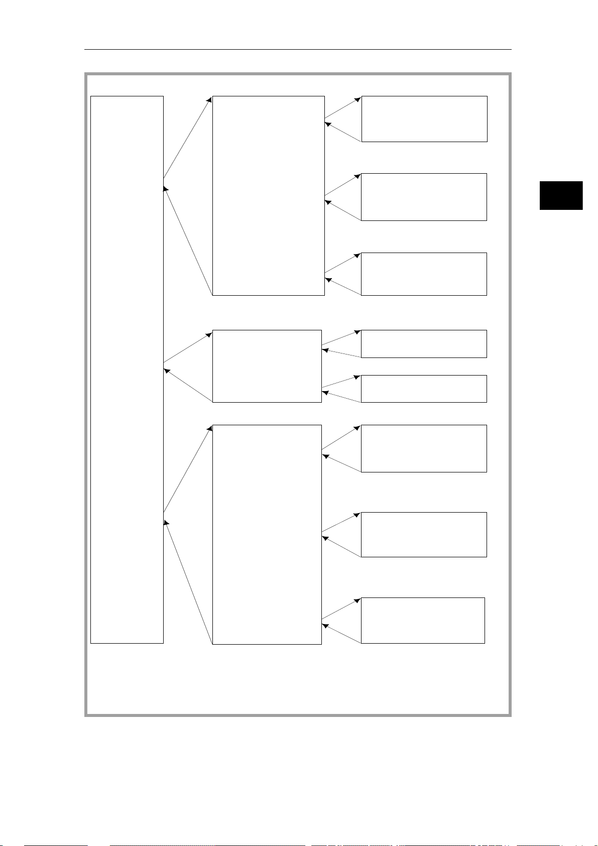
O
Program Organization
B1
JU PB ‘X‘
PB ‘X‘
Controlled
system part ‘X‘
FB
Individual control
FB
Closed loop control
3
PB ‘Y‘ FB
Controlled
system part ‘Y‘
JU PB ‘Y‘
FX
Signalling
Sequence control
FX
Signalling
FB ‘Z‘
Controlled
system part ‘Z‘
JU PB ‘Z‘
BE
FB
Closed loop control
FB
Arithmetic
FB
Data logging output
Fig. 3-3 Example of the organization of the user program according to the struct ure of th e control led system
CPU 948 Programming Guide
C79000-B8576-C848-03
3 - 7
Page 90

Program Organization
Nesting blocks
OB 1
JU
A
PB 5
F 200.5
*)
BE
*)
Operation to which the program returns
Fig. 3-4 Nested logic block calls
Fig. 3-4 shows the principle of nested block ca lls.
PB 5
1st STEP 5 op.
C
DB 20
PB 20
JU
O
F1.5
*)
BE
PB 20
1st STEP 5 op.
C
DB 30
FB 30
JU
NAME:
A
KURV
I 55.0
BE
*)
Block addresses
A block start address specif ies the location of a block in the user
memory. For logic block s, this is the ad dr ess of the me mo ry location
containing the first STEP 5 oper atio n (with FB and FX, the JU
operation via the formal operand list); with data blocks, it is the
address of the first data word.
To enable the CPU to locate the calle d blo ck in the memo ry , the start
addresses of all valid blocks are en ter ed in the blo ck addre ss list in
data block DB 0. DB 0 is managed by the system program, you cannot
call it yourself.
The CPU stores a return address every time a new block is called. After
the new block has been processed, this return address enables the program
to find the block from which the call originated. The return address is the
address of the memory location containing the next STEP 5 statement
after the block call. The CPU also stores the start address and length of
the data block valid at this location.
CPU 948 Programming Guide
3 - 8 C79000-B8576-C848-03
Page 91
Program Organization
Nesting depth
Example of nesting depth
Program
processing
level
You can only nest 40 blocks with in one an other. If more than 40
blocks are called , the CPU signals an er ro r and goes to the sto p mode.
OB 25
OB 13
OB 2
PB 131 FB 131
FB 21
3
OB 1
1
Fig. 3-5 Example of block nesting depth
You can determine the nesting depth of your program as follows:
- Add all the organization blocks you have programmed
(in the example: 4 OBs).
- Add the nesting depth of the individual organization blocks
(in the example : 2 + 2 + 1 + 0 = 5) .
- Add the two amounts together to obtain the program nesting depth
(in the example: 4 + 5 = nesting depth 9). It must not exceed a value of
40.
PB 1
2
FB 1
3
Nesting depth
4
5
6
7
89
CPU 948 Programming Guide
C79000-B8576-C848-03
3 - 9
Page 92

Storing Program and Data Blocks
3.3 Storing Program and Data Blocks
On the CPU 948, the user program runs sole ly in the internal RAM.
The user program including data blocks must, therefore, be loade d in
the CPU 948 user memory.
How do I load programs and
data blocks in the internal
RAM?
You can use the following methods:
•• You can load the individual logic and data blocks in the RAM
using your PG.
•• You can program a memory car d (flash EPROM!) with your
complete program inclu din g data blo ck s on the PG and then inse rt
the card in the receptacle on the CPU.
If you do an overall reset on the CPU (refer to Chapter 4) the
complete contents of the mem ory ca rd are loaded "1:1" in the
internal RAM.
•• You loaded your program in the inte rn al RAM with the PG or
from the memory car d with an OVERAL L RE SET . You can then
load additional blocks with the PG or replac e ex isting blocks.
Note
You can only program the memory card on the PG. Use the PG
software from version 6 upwards. When programming, the PG must
be in the mode "WORD FIELD" (refer to the STEP 5 manual /3/).
Caution
If you have changed or added blocks usin g the PG after loading
your program from the memory card, these changes are reversed
by the next OVERALL RESET, since the memory is
overwritten aga in with the con ten ts of the memor y ca rd .
CPU 948 Programming Guide
3 - 10 C79000-B8576-C848-03
Page 93

3.4 Processing the User Program
The complete software on the CPU (consisting of the system program
and the STEP 5 user program) ha s the following tasks:
•• CPU START-UP
•• Controlling an automatio n proc ess by con tinu ously repeating
operations (CYCLE).
•• Controlling an automatio n proc ess by reacting to events occurring
sporadically or at certain times (interrupts) and re ac ting to errors.
For all three tasks, you can selec t spec ial parts of your progra m to run
on the CPU by programming user inter faces (organizatio n blo cks
OB 1 to OB 35 - refer to Section 2.2.3).
Processing the User Program
3
START-UP
CYCLE
Before the CPU can start cyclic program execu tion , an initializ atio n
must be performed to establish a defin ed initial statu s for cyc lic
program execution and, for example , to spe cif y a time base for the
execution of certa in func tion s. Th e way in which this initialization is
performed depends on the even t that led to a START-UP and on
settings that you can make on your CPU. For more detailed
information, refer to Chapter 4.
You can influence the START-UP pr oc ed ure of your CPU by
programming organizatio n blo ck s OB 20, OB 21 and OB 22 or by
assigning paramete rs in DX 0 (re fe r to Chap ter 7).
Following the START-UP, the system program goes over to cyclic
processing. It is respon sible for bac kgro un d func tion s req uir ed for the
automation tasks (r ef er to Fig. 3- 1 at the beginn ing of this sec tion ).
After the system functions have been execu ted at the be ginning of a
CYCLE, the system program calls org aniza tion block OB 1 or
function block FB 0 as the cyclic user progr am . You progr am the
STEP 5 operations for cyclic proce ssing in this bloc k.
CPU 948 Programming Guide
C79000-B8576-C848-03
3 - 11
Page 94

Processing the User Program
Reactions to interrupts
and errors
To allow you to specify the re ac tion s to inter ru pts or error s, spe cia l
organization blocks (OB 2 to OB 18 for interrupt servicing, OB 19
and OB 23 to OB 34 for reactions to errors) are available on the
CPU 948. You can store an appropriate STEP 5 program in these blocks.
When interrupts or errors ar e to be proce ssed, the system program
activates the corresp on din g orga niz ation block during cyclic
processing. This means tha t the cy clic proce ssing is interr upted to
service an interrupt or to re ac t to an er ror. The nestin g of the
organization bloc ks ha s a fixed priority (for furthe r inf or ma tion, refer
to Chapters 4 and 5).
In addition to the organization blocks, you can also influe nc e the
reaction of the CPU to interrupt servicin g by assign ing param ete rs in
data block DX 0.
Organization block s OB 1 to OB 39 can be called by the syste m
program as soon as they are loaded in the program memory (also
during operation).
If the OBs are not loaded, ther e is eithe r no rea ctio n fr om the CPU or
(in the event of errors) it goe s to the stop mode (r ef er also to Sec tion
5.4).
You can also load data block DX 0 into the progr am memor y durin g
operation like the organization blocks. It is, however, only effective
after the next COLD RESTART. If DX 0 is not loaded, the standard
settings apply (refer to Chapter 7).
3.4.1 Definition of Terms used in Program Execution
Cycle time
The cycle begin s when the cy cle monitoring time is trigg er ed and ends
with the next trigger. The time tha t the CPU re qu ire s to exe cute the
program between two trigg er s is called the cycle time. The cycle time
consists of the runtime of the system program and the runtim e of the
user program.
The cycle time ther ef or e inc lud es the following:
•• the time required to process the cy clic progr am (syste m and use r
program),
•• the time required to proce ss in ter rupts (e.g. time-contro lled
interrupt),
•• the time required to proce ss interruptions (errors).
CPU 948 Programming Guide
3 - 12 C79000-B8576-C848-03
Page 95

Processing the User Program
Cycle time monitoring
Process input and output
image (PII and PIQ)
The CPU monitors the cycle time in case it exceeds a maximum value.
The standard setting for this maximum value is 200 ms. You can set the
cycle time monitoring yourself or restart it during user program execution
(refer to DX 0/Chapter 7 and special function OB OB 222/Section 6.16).
The process image of the inp uts an d outpu ts is a memo ry are a in the
internal RAM.
Before cyclic execution of the user program begins, the system
program reads the signa l states of the inp ut peripheral modules and
transfers them to the process input image. The user program evaluates
the signal states in the process inp ut image and then sets the
appropriate signal states for the outputs in the proce ss outp ut image.
After the user program has been proc esse d, the syste m prog ram
transfers the signal states of the pr ocess ou tput imag e to the output
peripheral modules.
Buffering the I/O signals in the process ima ge of the inpu ts and
outputs avoids a change in a bit within a progr am cyc le from cau sing
the corresponding output to "flutter".
The process image is ther ef or e a me mory are a who se co nte nts ar e
output to the peripherals and read in from the periph er als onc e per
cycle.
3
Interprocessor communication
(IPC) flags
Note
The process image only exists for input and output bytes of the "P"
peripherals with byte addresses from 0 to 127!
Apart from the process image integrated in the system, you can use
OB 126 to define and transfer further process images (refer to
Section 6.6)
IPC flags exchange data between individual CPUs (multiprocessing) or
between the CPU and some communication processors.
The system program reads the input IPC flags of the CPU before cyclic
execution of the user program begins. After the STEP 5 program is
processed, the system program transfers the output IPC flags to the
coordinator or to the communications processors.
You define the input and output IPC flags when you create data block
DB 1 (refer to Section 10.1.6).
CPU 948 Programming Guide
C79000-B8576-C848-03
3 - 13
Page 96

Processing the User Program
Interrupt events
Cyclic program execution can be interrupted by the following:
•• time-controlle d program execution (delaye d inte rrup t, cy clic timed
interrupts, clock-c ontrolled interrupts),
•• interrupt-drive n prog ra m ex ec utio n (pro ce ss interrupt, system
interrupt).
The cyclic program ca n be inter ru pte d or eve n abor ted com ple tely by
the following:
•• a device hardware fault or program error
•• operator intervention (using the P C stop fun ctio n, or setting the
mode selector to "stop", multiprocessor stop MP-STP),
•• a stop operation
CPU 948 Programming Guide
3 - 14 C79000-B8576-C848-03
Page 97

3.5 STEP 5 Operations with Example s
Low byte
8 7
ACCU-1-LL
A STEP 5 operation consists of the operation and an operand. The
operation specifies what the CPU is to do (operation). Th e op er an d
specifies with what an ope ra tion is to be executed.
STEP 5 operations ca n be divid ed into the following group s:
STEP 5 Operations with Examples
Accumulators as working
registers
High word
ACCU 1
1)
High byte
31
ACCU-1-HH
ACCU-1-H
24 23
•• basic operations (can be used in all logic blocks),
•• supplementary operations,
•• executive operations (can only be used in FB/FX function blocks),
•• semaphore operatio ns (c an only be use d in FB/FX func tion bloc ks) .
The CPU 948 has four accumulators, ACCU 1 to ACCU 4. Most
STEP 5 operations use two 32-bit registers (ACCU 1 and ACCU 2) as
the source of opera nds a nd the de stina tion for resu lts.
Low word
Low byte
16 15
ACCU-1-HL
High byte
0
ACCU-1-LH
ACCU-1-L
3
1)
analogous for ACCU 2 to ACCU 4
CPU 948 Programming Guide
C79000-B8576-C848-03
The STEP 5 operation to be car rie d out aff ec ts the ac cu mu lato rs, e.g .:
•• ACCU 1 is always the destination in load ope ra tion s. A load
operation shifts the old conten ts of ACCU 1 to ACCU 2 (stack
lift). Accumulator s 3 and 4 are not ch ange d by any load ope ra tion s.
3 - 15
Page 98

STEP 5 Operations with Examples
•• Arithmetic operations combine the contents of ACCU 1 with those
•• When a constant is added (ADD BF/KF/DH) to the contents of
of ACCU 2, write the result to ACCU 1 and transfer the contents
of ACCU 3 to ACCU 2 and the contents of ACCU 4 to ACCU 3
(stack drop). In 16-bit fix ed poin t arith metic, only the low word or
ACCU 3 is transferred to the low word of ACCU 2 and the low
word of ACCU 4 to the low word of ACCU 3.
ACCU 1, the accumulators 2, 3 and 4 are not changed.
Condition codes
Bit condition codes
STEP 5 operations either set or evaluate condition codes. The condition
codes are written to a condition code byte. Two groups of condition codes
can be distinguished: condition codes of digital operations (word
condition codes - bits 4 to 7 in the condition code byte) and condition
codes from binary and executive operations (bit condition codes - bits 0 to
3 in the condition code byte). You can see how the various condition
codes are influenced or evaluated by STEP 5 operations be referring to
the operation list /1/.
You can display the condition cod e byte on a program me r usin g the
"STATUS" online function (ref er to Sectio n 11.2 .3 ). The byte has the
following structure:
Word condition codes Bit condition codes
CC 1 CC 0 OV OS OR STA RLO
ERAB
Bit 7 6 5 4 3 2 1 0
•• ERAB First bit scan
A logic operation sequence containing binary operations always
begins with the first bit scan, following whic h a new RLO is
formed. The bit condition code
ERAB = 1 is then set. While the
remaining logic op er atio ns in the sequence are bein g perf or me d,
ERAB remains set to 1 and the RLO cannot be changed by these
logic operations.
The active sequence of logic op er atio ns is t erminat ed by a binary
set/reset operation (e.g. S Q 5.0). The set/reset op eratio n sets
ERAB to 0; the RLO can be evaluated (e.g. by RLO-dep en dent
operations) but ca n no longer be combined logica lly. The next
binary logic operatio n following a binary set/reset opera tion is
once again a first bit scan.
CPU 948 Programming Guide
3 - 16 C79000-B8576-C848-03
Page 99

Example of ERAB
STEP 5 Operations with Examples
:A I 1.0 ERAB is set to ’1’,
: the new RLO is formed by
: an AND operation
:O I 6.3 The RLO is influenced by
: an OR operation
:AN I 2.1 The RLO is influenced by
: an AND NOT operation.
:S Q 2.4 ERAB is set to ’0’,
: the sequence is now complete
:JC FB 150 The function block is called
: dependent on the RLO.
:
:
3
Other bit condition codes
Word condition codes
•• RLO Result of logic operation
This is the result of bit logic operations. It is the truth statem en t for
comparison operation s ( re fe r to oper atio ns list, bin ary logic
operations or compariso n oper ations).
•• STA Status
For bit operations, this indica tes the logic al statu s of the bit just
scanned or set. The status is update d in binary logic operations except for A(, O(,), O and for set/reset operations.
•• OR Or
Internal CPU bit for handling "AND before OR" log ic oper ations.
•• OV Overflow
This indicates whether the permissible number range was exceeded
during the arithmetic operation just completed.
CPU 948 Programming Guide
C79000-B8576-C848-03
•• OS Stored over flo w
The overflow bit is stored. It can be used in several arithmetic
operations to indicate whether an overflow occurred at any point
during the operations.
3 - 17
Page 100

STEP 5 Operations with Examples
•• CC 1 and CC 0
These are the result condition codes that you can interpret from the
following table:
Note
To evaluate the condition codes directly, comparison and jump
operations are available (refer to Sections 3.5.1 and 3.5.3).
Table 3-1 Result condition codes of STEP 5 operations
Word
condition codes
Arith-
metical
operations
CC 1 CC 0
0 0 Result
0 1 Result
1 0 Result
1 1 Division
= 0
Digital
logic
operations
Result
= 0
Com-
parison
operations
ACCU 2
=
ACCU 1
Shift
operations
Shifted
bit
= 0
For
SED,
SEE
Semaphore
set
ACCU 2
< 0 –
<
––JMJN
ACCU 1
> 0
Result
≠ 0
ACCU 2
>
ACCU 1
Shifted
bit
= 1
Semaphore
set
enabled
by 0 – – – –
Note
When a change of level takes place, e.g. servicing a timed interrupt,
all accumulators and the bit and word condition codes (RLO etc.) are
saved and loaded again when the interrupted level is resumed.
or
Jump
operations
executed
is
JZ
JP
is
JN
–
CPU 948 Programming Guide
3 - 18 C79000-B8576-C848-03
 Loading...