

Page 1
Information and Communication
Communication Devices
S11 / S11 MMI
Repair Documentation
Level 2.5
V 1.2
V1.2 Page 1 of 49 ICP CD ST
D. Schnoor
06/98
Page 2

Information and Communication
Communication Devices
Table of Contents:
1 INTRODUCTION................................................................................................................................................3
2 ANTENNA SPRING
...................................................................................................................................................................................4
3 TCXO
...................................................................................................................................................................................7
4 FUSE 1A
.................................................................................................................................................................................10
5 FUSE 0.25 A
.................................................................................................................................................................................14
6 MOLEX CONNECTOR
.................................................................................................................................................................................19
7 RINGER
.................................................................................................................................................................................23
8 CARDREADER
.................................................................................................................................................................................27
9 VOLUMESLIDER
.................................................................................................................................................................................31
10 MEMOSWITCH
.................................................................................................................................................................................35
11 ANTENNASWITCH
.................................................................................................................................................................................39
12 COIL
.................................................................................................................................................................................44
V1.2 Page 2 of 49 ICP CD ST
D. Schnoor
06/98
Page 3

Information and Communication
Communication Devices
1Introduction
The product familiy S1x consists of S10 (GSM-900), S11 (GSM-1800) and S12
(GSM-1900). The S10 is also available as a special outdoor version, the S10 Active. This
phone has different display and RF/Control modules, even though many of the components
are identical.
This manual is intended to help you carry out S11 repairs on level 2.5, meaning limited
component repairs. Failure highlights are documented and should be repaired in the local
workshops.
It must be noted that all repairs have to be carried out in an environment set up according to
the ESD (Electrostatic Discharge Sensitive Devices) regulations defined in international
standards.
If you have any questions regarding the repair procedures or spare parts do not hesitate to
contact our technical support team in Kamp-Lintfort, Germany:
Tel.: +49 2842 95 4666
Fax: +49 2842 95 4302
e-mail: dominik.schnoor@klf.siemens.de
V1.2 Page 3 of 49 ICP CD ST
D. Schnoor
06/98
Page 4

Information and Communication
Communication Devices
2Antenna Spring
2.1Affected Units
2.1.1Type: S11
2.1.2Affected IMEIs / Date Codes: All / All
2.1.3Affected SW-Versions: All
2.1.4Fault Code for LSO reporting: 3ANS
2.2Fault Description
2.2.1Fault Symptoms for customers:
Customers experience problems registering to the
network and making calls.
2.2.2Fault Symptom on GSM-Tester:
The GSM-Tester will show a low Tx-Power only on the
internal antenna (aerial coupler measurement!).
2.3Priority:
V1.2 Page 4 of 49 ICP CD ST
D. Schnoor
06/98
Page 5

Information and Communication
Communication Devices
........ Mandatory
........ Repair
........ Optional
........ Not Yet Defined
2.4Repair Documentation
2.4.1Description of procedure:
2.4.1.1Diagnosis
Visually check the status of the antenna spring. Look for a bent
contact or dry soldering joint.
2.4.1.2Repair by component change
Use soldering iron to remove defective spring.
Resolder new spring afterwards.
2.4.1.3Repair by SW-Booting
Not possible!
2.4.1.4Test
Retest handset after repair.
2.4.2List of needed material
2.4.2.1Components
Antenna Spring
V1.2 Page 5 of 49 ICP CD ST
D. Schnoor
06/98
Page 6
Information and Communication
Communication Devices
Part-Number: L36158-A11-C23
2.4.2.2 Jigs and Tools
Soldering Iron
2.4.2.3Special Tools
None
2.4.2.4Working materials
Desolder Wick / Braid
Solder
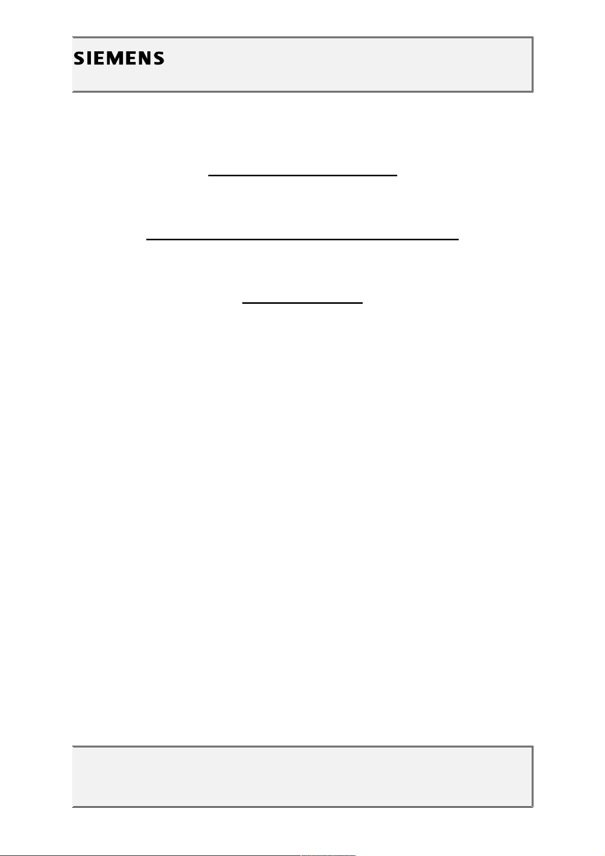
2.4.3Drawings
V1.2 Page 6 of 49 ICP CD ST
D. Schnoor
06/98
Figure 1: S11 Board Antenna Spring Side
Figure 2: S11 Antenna Spring (X900) Placement (Top View)
Page 7
Information and Communication
Communication Devices
3TCXO
3.1Affected Units
3.1.1Type: S11
3.1.2Affected IMEIs / Date Codes: All / All
3.1.3Affected SW-Versions: All
3.1.4Fault Code for LSO reporting: 3TCX
3.2Fault Description
3.2.1Fault Symptoms for customers:
Network Search
Handset not logging into network
3.2.2Fault Symptom on GSM-Tester:
Frequency error in synchronized mode >90 Hz
No location update possible
The TCXO (Temperature Compensated Crystal Oscillator) is responsible for generating the
13 MHz reference frequency of the handset.
If it is defective, the handset cannot synchronize to the base station anymore.
V1.2 Page 7 of 49 ICP CD ST
D. Schnoor
06/98
Buffer
Lowpass
VC OUT 13MHz
SIN13MHz
(from µP)
AFC_PNM
TCXO
DC Voltage
Page 8

Information and Communication
Communication Devices
All other frequencies are derived from this 13MHz reference, its stability is vital for the
handset function.
The TCXO output frequency is determined by a DC tuning voltage applied to its VC pin. The
voltage comes from the microprocessor as a pulse number modulated digital signal.
A lowpass then converts this digital signal to a proportional DC voltage, which is then used
to fine tune the TCXO output frequency.
3.3Priority:
........ Mandatory
........ Repair
........ Optional
........ Not Yet Defined
3.4Repair Documentation
3.4.1Description of procedure:
3.4.1.1Diagnosis
Check the output frequency of the TCXO using the level-2 testing
program for S11.
Switch off the „CMD in Use“ option in the config file (S6xx.CFG or
S6xx.INI depending on the version of the testsoftware) and restart
the program. Start the S11 test, when the program says „Check power
and phase of external antenna with your GSM-Tester“, switch the
CMD to „LOCAL“ mode and enter the „MODULE TEST“.
On the CMD display you can see the frequency error of the handset.
(Make sure that the CMD is on channel number defined in the [PCN]
section of the S6xx.ini, power level 0!)
If the frequency error is higher than 2kHz, the TCXO has to be
replaced.
3.4.1.2Repair by component change
Use hot air blower to remove defective TCXO.
V1.2 Page 8 of 49 ICP CD ST
D. Schnoor
06/98
Page 9

Information and Communication
Communication Devices
Avoid excessive heat!
Watch surrounding components!
Resolder new TCXO afterwards.
3.4.1.3Repair by SW-Booting
Not possible!
3.4.1.4Test
Retest handset after repair as described above.
The frequency error must now be < 2kHz.
3.4.2List of needed material
3.4.2.1Components
TCXO
Part-Number: L36145-G300-Y17
3.4.2.2 Jigs and Tools
Hot Air Blower
Soldering Iron
3.4.2.3Special Tools
None
3.4.2.4Working materials
Desolder Wick / Braid
Solder
V1.2 Page 9 of 49 ICP CD ST
D. Schnoor
06/98
Page 10
Information and Communication
Communication Devices
3.4.3Drawings
4Fuse
1A
4.1Affecte d Units
4.1.1Type:
S11
MMI
V1.2 Page 10 of 49 ICP CD ST
D. Schnoor
06/98
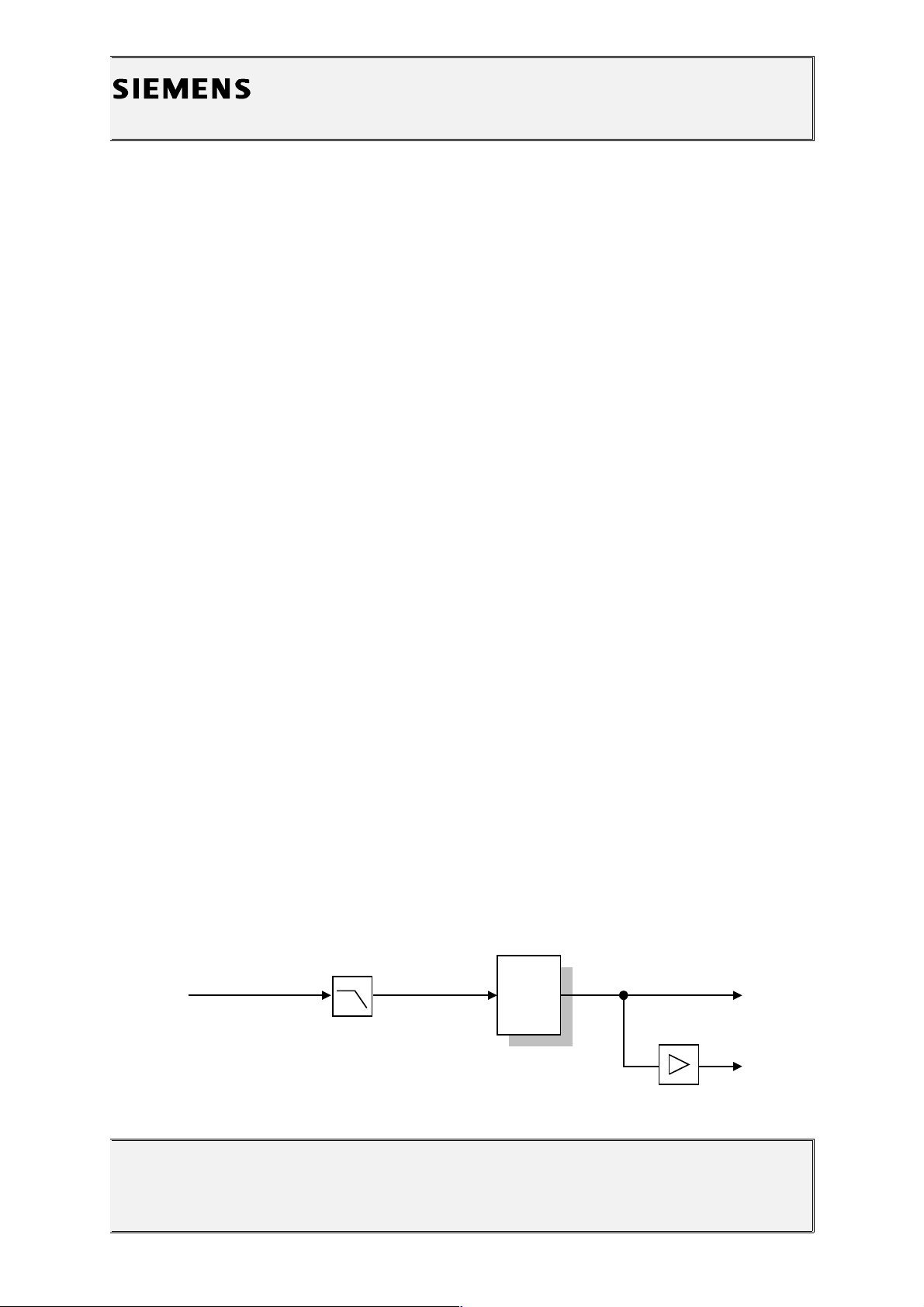
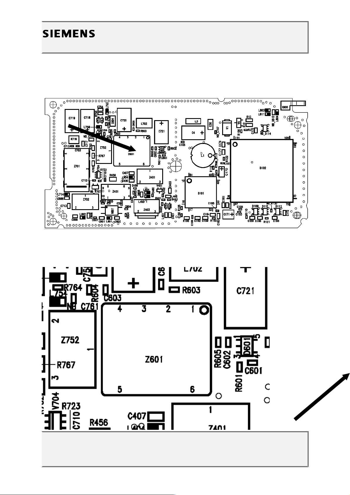
Figure 1: S11 Board TCXO Side
Figure 2: S11 TCXO (Z601) Placement (Top View)
Page 11

Information and Communication
Communication Devices
4.1.2Affected IMEIs / Date Codes: All / All
4.1.3Affected SW-Versions: All
4.1.4Fault Code for LSO reporting: 3FU1
4.2Fault Description
4.2.1Fault Symptoms for customers:
Battery charging not possible
4.2.2Fault Symptom on GSM-Tester:
This fault cannot be detected with a GSM-Tester
4.3Priority:
........ Mandatory
........ Repair
........ Optional
........ Not Yet Defined
4.4Repair Documentation
4.4.1Description of procedure:
4.4.1.1Diagnosis
Check the status of the fuse by measuring its resistance with
V1.2 Page 11 of 49 ICP CD ST
D. Schnoor
06/98
Page 12

Information and Communication
Communication Devices
a multimeter. The fuse is defective if the resitance higher than 10
ohms
4.4.1.2Repair by component change
Use soldering iron to remove defective fuse.
Avoid excessive heat!
Watch surrounding components!
Resolder new fuse afterwards.
4.4.1.3Repair by SW-Booting
Not possible!
4.4.1.4Test
Retest handset after repair as described above.
The resistance must now be close to zero.
4.4.2List of needed material
4.4.2.1Components
Fuse
V1.2 Page 12 of 49 ICP CD ST
D. Schnoor
06/98
Page 13

Information and Communication
Communication Devices
Part-Number: L36145-A820-Y7
4.4.2.2Jigs and Tools
Soldering Iron
4.4.2.3Special Tools
Multimeter
4.4.2.4Working materials
Desolder Wick / Braid
Solder
4.4.3Drawings
V1.2 Page 13 of 49 ICP CD ST
D. Schnoor
06/98
Page 14
Information and Communication
Communication Devices
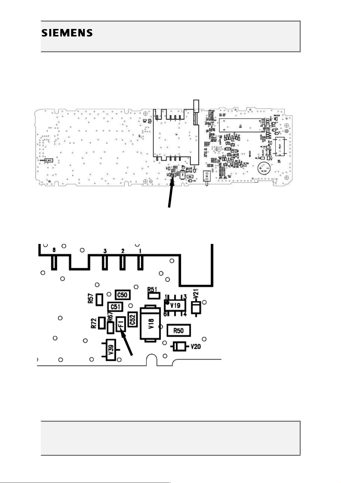
5Fuse 0.25 A
V1.2 Page 14 of 49 ICP CD ST
D. Schnoor
06/98
Figure 1: S11 MMI Board 1A Fuse Side
Figure 2: 1A Fuse (F1) Placement (Top View)
Page 15
Information and Communication
Communication Devices
5.1Affected Units
5.1.1Type: S11 MMI
5.1.2Affected IMEIs / Date Codes: All / All
5.1.3Affected SW-Versions: All
5.1.4Fault Code for LSO reporting: 3FU2
5.2Fault Description
5.2.1Fault Symptoms for customers:
Supplying of external accessories through the handset’s
bottom connector is not possible
5.2.2Fault Symptom on GSM-Tester:
This fault cannot be detected with a GSM-Tester
5.3Priority:
........ Mandatory
........ Repair
........ Optional
........ Not Yet Defined
V1.2 Page 15 of 49 ICP CD ST
D. Schnoor
06/98
Page 16

Information and Communication
Communication Devices
5.4Repair Documentation
5.4.1Description of procedure:
5.4.1.1Diagnosis
Check the status of the fuse by measuring its resistance with
a multimeter. The fuse is defective if the resitance higher than 10
ohms
5.4.1.2Repair by component change
Use soldering iron to remove defective fuse.
Avoid excessive heat!
Watch surrounding components!
Resolder new fuse afterwards.
5.4.1.3Repair by SW-Booting
Not possible!
5.4.1.4Test
Retest handset after repair as described above.
The resistance must now be close to zero.
V1.2 Page 16 of 49 ICP CD ST
D. Schnoor
06/98
Page 17

Information and Communication
Communication Devices
5.4.2List of needed material
5.4.2.1Components
Fuse
Part-Number: L36145-A820-Y10
5.4.2.2Jigs and Tools
Soldering Iron
5.4.2.3Special Tools
Multimeter
5.4.2.4Working materials
Desolder Wick / Braid
Solder
V1.2 Page 17 of 49 ICP CD ST
D. Schnoor
06/98
Page 18

Information and Communication
Communication Devices
5.4.3Drawings
V1.2 Page 18 of 49 ICP CD ST
D. Schnoor
06/98
Figure 1: S11 MMI Board 0.25A Fuse Side
Figure 2: 0.25A Fuse (F2) Placement (Top View)
Page 19

Information and Communication
Communication Devices
6Molex Connector
6.1Affected Units
6.1.1Type: S11 MMI
6.1.2Affected IMEIs / Date Codes: All / All
6.1.3Affected SW-Versions: All
6.1.4 Fault Code for LSO reporting: 3MOC
6.2Fault Description
6.2.1Fault Symptoms for customers:
Charging or operation in a car kit not possible.
6.2.2Fault Symptom on GSM-Tester:
Output power problems on the external antenna only.
6.3Priority:
........ Mandatory
........ Repair
........ Optional
........ Not Yet Defined
V1.2 Page 19 of 49 ICP CD ST
D. Schnoor
06/98
Page 20

Information and Communication
Communication Devices
6.4Repair Documentation
6.4.1Description of procedure:
6.4.1.1Diagnosis
Visually check the bottom connector. Watch for dry joints.
6.4.1.2Repair by component change
Use hot air blower to remove defective connector.
Avoid excessive heat!
Watch surrounding components!
Resolder new connector afterwards.
Make sure that you use just very little flux, otherwise the connector
contacts can become dirty.
6.4.1.3Repair by SW-Booting
Not possible!
6.4.1.4Test
Retest handset after repair.
V1.2 Page 20 of 49 ICP CD ST
D. Schnoor
06/98
Page 21

Information and Communication
Communication Devices
6.4.2List of needed material
6.4.2.1Components
Molex Connector
Part-Number: L36334-Z93-C244
6.4.2.2Jigs and Tools
Hot Air Blower
Soldering Iron
6.4.2.3Special Tools
None
6.4.2.4Working materials
Desolder Wick / Braid
Solder
Flux
V1.2 Page 21 of 49 ICP CD ST
D. Schnoor
06/98
Page 22

Information and Communication
Communication Devices
6.4.3Drawings
V1.2 Page 22 of 49 ICP CD ST
D. Schnoor
06/98
Figure 1: S11 MMI Board Bottom Connector Side
Figure 2: Bottom Connector Placement (Top View)
Page 23

Information and Communication
Communication Devices
7Ringer
7.1Affected Units
7.1.1Type: S11 MMI
7.1.2Affected IMEIs / Date Codes: All / All
7.1.3Affected SW-Versions: All
7.1.4Fault Code for LSO reporting: 3RIN
7.2Fault Description
V1.2 Page 23 of 49 ICP CD ST
D. Schnoor
06/98
Page 24

Information and Communication
Communication Devices
7.2.1Fault Symptoms for customers:
No ringer tone audible or ringer tone distorted.
7.2.2Fault Symptom on GSM-Tester:
Ringer check fails.
7.3Priority:
........ Mandatory
........ Repair
........ Optional
........ Not Yet Defined
7.4Repair Documentation
7.4.1Description of procedure:
7.4.1.1Diagnosis
Check ringer functionality either manually with testing program.
7.4.1.2Repair by component change
Use hot air blower remove defective ringer.
Avoid excessive heat!
Watch surrounding components, especially the display window!
To protect the display, you can also desolder the ringer with solder
wick.
Resolder new ringer afterwards.
Watch placement of ringer!
7.4.1.3Repair by SW-Booting
V1.2 Page 24 of 49 ICP CD ST
D. Schnoor
06/98
Page 25

Information and Communication
Communication Devices
Not possible!
7.4.1.4Test
Retest handset after repair.
7.4.2List of needed material
7.4.2.1Components
Ringer
Part-Number: L36178-Z2-C15
7.4.2.2Jigs and Tools
Hot Air Blower
Soldering Iron
7.4.2.3Special Tools
None
7.4.2.4Working materials
Desolder Wick / Braid
V1.2 Page 25 of 49 ICP CD ST
D. Schnoor
06/98
Page 26

Information and Communication
Communication Devices
Solder
7.4.3Drawings
V1.2 Page 26 of 49 ICP CD ST
D. Schnoor
06/98
Figure 1: S11 MMI Board Ringer Side
Figure 2: Ringer (B1) Placement (Top View)
Page 27

Information and Communication
Communication Devices
8Cardreader
8.1Affected Units
8.1.1Type: S11 MMI
8.1.2Affected IMEIs / Date Codes: All / All
8.1.3Affected SW-Versions: All
8.1.4Fault Code for LSO reporting: 3REA
8.2Fault Description
8.2.1Fault Symptoms for customers:
Sim card is not accepted or properly read by
the handset.
Sim card ejection mechanism may be damaged.
8.2.2Fault Symptom on GSM-Tester:
V1.2 Page 27 of 49 ICP CD ST
D. Schnoor
06/98
Page 28

Information and Communication
Communication Devices
When testing with a test-simcard the above
symptoms will come up.
8.3Priority:
........ Mandatory
........ Repair
........ Optional
........ Not Yet Defined
8.4Repair Documentation
8.4.1Description of procedure:
8.4.1.1Diagnosis
Check cardreader functionality with sim card.
Attention: Watch for dry joints (especially pin 7!) or mechanical
damage.
8.4.1.2Repair by component change
Resolder dry joints.
If the cardreader is mechanically damaged use solder wick to remove
defective component.
Avoid excessive heat!
Watch surrounding components!!
Resolder new cardreader afterwards.
8.4.1.3Repair by SW-Booting
Not possible!
V1.2 Page 28 of 49 ICP CD ST
D. Schnoor
06/98
Page 29

Information and Communication
Communication Devices
8.4.1.4Test
Retest handset after repair.
8.4.2List of needed material
8.4.2.1Components
Cardreader
Part-Number: L36334-Z95-C994
8.4.2.2Jigs and Tools
Soldering Iron
8.4.2.3Special Tools
None
8.4.2.4Working materials
Desolder Wick / Braid
Solder
V1.2 Page 29 of 49 ICP CD ST
D. Schnoor
06/98
Page 30

Information and Communication
Communication Devices
8.4.3Drawings
V1.2 Page 30 of 49 ICP CD ST
D. Schnoor
06/98
Figure 1: S11 MMI Board Cardreader Side
Page 31

Information and Communication
Communication Devices
9Volumeslider
9.1Affected Units
9.1.1Type: S11 MMI
9.1.2Affected IMEIs / Date Codes: All / All
V1.2 Page 31 of 49 ICP CD ST
D. Schnoor
06/98
Figure 2: Cardreader Placement (Top View)
Page 32

Information and Communication
Communication Devices
9.1.3Affected SW-Versions: All
9.1.4Fault Code for LSO reporting: 3VSL
9.2Fault Description
9.2.1Fault Symptoms for customers:
The volume slider does not work properly.
9.2.2Fault Symptom on GSM-Tester:
During the keyboard test, the volume slider fails.
9.3Priority:
........ Mandatory
........ Repair
........ Optional
........ Not Yet Defined
9.4Repair Documentation
9.4.1Description of procedure:
9.4.1.1Diagnosis
Check volumeslider functionality either manually or with the
testing program.
Watch for dry joints or mechanical damage.
V1.2 Page 32 of 49 ICP CD ST
D. Schnoor
06/98
Page 33

Information and Communication
Communication Devices
9.4.1.2Repair by component change
Use solder wick to remove defective slider.
Avoid excessive heat!
Watch surrounding components!!
Resolder new volumeslider afterwards.
9.4.1.3Repair by SW-Booting
Not possible!
9.4.1.4Test
Retest handset after repair.
9.4.2List of needed material
9.4.2.1Components
Volumeslider
Part-Number: L36315-Z77-C186
9.4.2.2Jigs and Tools
V1.2 Page 33 of 49 ICP CD ST
D. Schnoor
06/98
Page 34

Information and Communication
Communication Devices
Soldering Iron
9.4.2.3Special Tools
None
9.4.2.4Working materials
Desolder Wick / Braid
Solder
9.4.3Drawings
V1.2 Page 34 of 49 ICP CD ST
D. Schnoor
06/98
Figure 1: S11 MMI Board Volumeslider Side
Page 35

Information and Communication
Communication Devices
10Memoswitch
10.1Affected Units
V1.2 Page 35 of 49 ICP CD ST
D. Schnoor
06/98
Figure 2: Volumeslider Placement (Top View)
Page 36

Information and Communication
Communication Devices
10.1.1Type: S11 MMI
10.1.2Affected IMEIs / Date Codes: All / All
10.1.3Affected SW-Versions: All
10.1.4Fault Code for LSO reporting: 3MSW
10.2Fault Description
10.2.1Fault Symptoms for customers:
The memoswitch does not work properly.
10.2.2Fault Symptom on GSM-Tester:
During the keyboard test, the memobutton fails.
10.3Priority:
........ Mandatory
........ Repair
........ Optional
........ Not Yet Defined
10.4Repair Documentation
10.4.1Description of procedure:
V1.2 Page 36 of 49 ICP CD ST
D. Schnoor
06/98
Page 37

Information and Communication
Communication Devices
10.4.1.1Diagnosis
Check memoswitch functionality either manually or with the
testing program.
Watch for dry joints or mechanical damage.
10.4.1.2Repair by component change
Use solder wick or hot air to remove defective switch.
Avoid excessive heat!
Watch surrounding components!!
Resolder new memoswitch afterwards.
10.4.1.3Repair by SW-Booting
Not possible!
10.4.1.4Test
Retest handset after repair.
10.4.2List of needed material
10.4.2.1Components
V1.2 Page 37 of 49 ICP CD ST
D. Schnoor
06/98
Page 38

Information and Communication
Communication Devices
Memoswitch
S11 Part-Number: L36315-Z77-C185
10.4.2.2Jigs and Tools
Soldering Iron
Hot Air
10.4.2.3Special Tools
None
10.4.2.4Working materials
Desolder Wick / Braid
Solder
10.4.3Drawings
V1.2 Page 38 of 49 ICP CD ST
D. Schnoor
06/98
Figure 1: S11 MMI Board Memoswitch Side
Page 39

Information and Communication
Communication Devices
11Antennaswitch
V1.2 Page 39 of 49 ICP CD ST
D. Schnoor
06/98
Figure 2: Memoswitch Placement (Top View)
Page 40

Information and Communication
Communication Devices
11.1Affected Units
11.1.1Type: S11
11.1.2Affected IMEIs / Date Codes: All / All
11.1.3Affected SW-Versions: All
11.1.4Fault Code for LSO reporting: 3ASW
11.2Fault Description
11.2.1Fault Symptoms for customers:
Problems with location update and call setup.
Network search.
11.2.2Fault Symptom on GSM-Tester:
Handset fails with low Tx power on both or either
antenna.
No location update possible.
11.3Priority:
........ Mandatory
........ Repair
........ Optional
........ Not Yet Defined
11.4Repair Documentation
11.4.1Description of procedure:
V1.2 Page 40 of 49 ICP CD ST
D. Schnoor
06/98
Page 41

Information and Communication
Communication Devices
11.4.1.1Diagnosis
The antennaswitch is used to switch the Rx and Tx path between the
internal an external antenna of the handset
The function of the antennaswitch can be verified by simple resistance
measurements:
Pin 2 and 7 against ground must be around 86 kOhms.
If any of these resistances are significantly different, the
antennaswitch will have to be replaced.
11.4.1.2Repair by component change
Use solder wick or hot air to remove defective switch.
Avoid excessive heat!
Watch surrounding components!!
Resolder new antennaswitch afterwards.
11.4.1.3Repair by SW-Booting
Not possible!
11.4.1.4Test
Retest handset after repair.
11.4.2List of needed material
11.4.2.1Components
Antennaswitch
Part-Number: L36810-U6013-D670
11.4.2.2Jigs and Tools
Soldering Iron
V1.2 Page 41 of 49 ICP CD ST
D. Schnoor
06/98
Page 42

Information and Communication
Communication Devices
Hot Air Blower
11.4.2.3Special Tools
None
11.4.2.4Working materials
Desolder Wick / Braid
Solder
11.4.3Drawings
V1.2 Page 42 of 49 ICP CD ST
D. Schnoor
06/98
Figure 1: S11 Board Antennaswitch Side
Figure 2: Antennaswitch (N801) Placement (Top View)
Page 43

Information and Communication
Communication Devices
V1.2 Page 43 of 49 ICP CD ST
D. Schnoor
06/98
Page 44

Information and Communication
Communication Devices
12Coil
12.1Affected Units
V1.2 Page 44 of 49 ICP CD ST
D. Schnoor
06/98
Page 45

Information and Communication
Communication Devices
12.1.1Type: S11
12.1.2Affected IMEIs / Date Codes: All / All
12.1.3Affected SW-Versions: All
12.1.4Fault Code for LSO reporting: 3COI
12.2Fault Description
12.2.1Fault Symptoms for customers:
Loud humming noise in loudspeaker.
12.2.2Fault Symptom on GSM-Tester:
Handset fails with loud humming noise in echo loop.
12.3Priority:
........ Mandatory
........ Repair
........ Optional
........ Not Yet Defined
12.4Repair Documentation
V1.2 Page 45 of 49 ICP CD ST
D. Schnoor
06/98
Page 46

Information and Communication
Communication Devices
12.4.1Description of procedure:
12.4.1.1Diagnosis
The coil is used in the step up converter which is generating a
6.0 V supply voltage for the power amplifier out of the 2.8V battery
voltage.
If the coil is mechanically damaged (broken) it produces heavy
interference with the acoustical elements of the S11 resulting in a loud
humming noise in the earpiece.
A broken coil can easily be diagnosed by trying to move it with two
fingers. If it moves, the core is broken and the coil has to be
replaced.
12.4.1.2Repair by component change
Use hot air to remove defective coil.
Avoid excessive heat!
Watch surrounding components!!
Resolder new coil afterwards
12.4.1.3Repair by SW-Booting
Not possible!
12.4.1.4Test
Retest handset after repair, by checking the audio quality with the
echo loop of the testprogram.
12.4.2List of needed material
V1.2 Page 46 of 49 ICP CD ST
D. Schnoor
06/98
Page 47

Information and Communication
Communication Devices
12.4.2.1Components
Part-Number: L36151-F5273-M2
12.4.2.2Jigs and Tools
Soldering Iron
Hot Air Blower
12.4.2.3Special Tools
None
12.4.2.4Working materials
Desolder Wick / Braid
Solder
12.4.3Drawings
V1.2 Page 47 of 49 ICP CD ST
D. Schnoor
06/98
Page 48

Information and Communication
Communication Devices
V1.2 Page 48 of 49 ICP CD ST
D. Schnoor
06/98
Figure 1: S11 Board Coil (L1) Side
Page 49

Information and Communication
Communication Devices
V1.2 Page 49 of 49 ICP CD ST
D. Schnoor
06/98
Figure 2: 27nH Coil (L1) Placement (Top View)
 Loading...