

Siemens MOC8111 Datasheet
W
MOC8111
PHOTOTRANSISTOR
NO BASE CONNECTION OPTOCOUPLER
FEATURES
NE
• Current Transfer Ratio 20% Min.
• No Base Terminal Connection for Improved
Common Mode Interface Immunity
• Field-Effect Stable by TRIOS (TRansparent
IOn Shield)
• Long T erm Stability
• Industry Standard Dual-in-Line Package
• Underwriters Lab File #E52744
V
• VDE 0884 Available with Option 1
DE
DESCRIPTION
The MOC8111 is an optocoupler consisting of a
Gallium Arsenide infrared emitting diode optically coupled to a silicon planar phototransistor
detector in a plastic plug-in DIP 6 pin package.
The coupling device is suitable for signal transmission between two electrically separated circuits. The potential difference between the
circuits to be coupled is not allowed to exceed
the maximum permissible reference voltages.
In contrast to the IL1 the base terminal is not connected, resulting in a substantially improved common-mode interference immunity.
Maximum Ratings (T
=25 ° C)
A
Emitter
Reverse Voltage .............................................. 6 V
DC Forward Current ...................................60 mA
Surge Forward Current (t ≤
10 µ s).................. 2.5 A
Total Power Dissipation............................ 100 mW
Detector
Collector-Emitter Breakdown Voltage............ 30 V
Collector Current ....................................... 50 mA
Collector Current (t ≤
1 ms) ........................ 150 mA
Total Power Dissipation............................ 150 mW
Package
Isolation Test Voltage between
Emitter and Detector, Refer to
Standard Climate 23/50
DIN 50014....................................5300 VAC
Creepage ................................................... ≥ 7 mm
Clearance................................................... ≥
7 mm
Isolation Thickness between
Emitter and Detector............................ ≥
0.4 mm
Comparative Tracking Index
per DIN IEC 112/VDE 0303, part 1 ..............175
Isolation Resistance
V
=500 V, T
IO
V
=500 V, T
IO
=25 ° C.................................10
A
=100 ° C...............................10
A
Storage Temperature Range ..... –55 ° C to +150 ° C
Ambient Temperature Range..... –55 °
C to +100 ° C
Soldering Temperature (max. 10 s,
dip soldering distance to
seating plane ≥
1.5 mm)...........................260 ° C
RMS
12
11
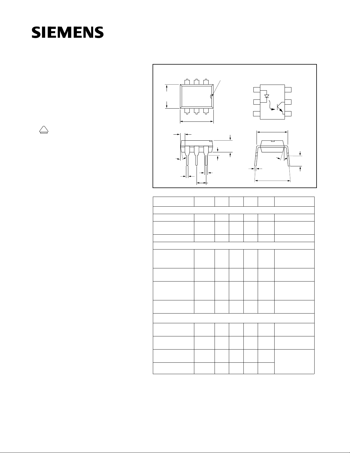
Package Dimensions in inches (mm)
Pin One ID.
5
I
BV
I
V
C
V
I
T
T
R
CEO
C
12
6
F
J
CEO
ECO
CE
CESAT
ON
OFF
Anode
1
Cathode
.130 (3.30)
.150 (3.81)
.020 (.051) min.
.031 (0.80)
.035 (0.90)
.100 (2.54) typ.
(T
=25 ° C)
A
1.15 1.5 V I
0.05 10 µ AV
25 pF V=0, f=1 MHz
30 V I
150nAV
7VI
7pFV
0.15 0.4 V I
2 5 mA I
7.5 20 µ
5.7 20 µ
NC
2
3
.300 (7.62)
18° typ.
.010 (.25)
.014 (.35)
.300 (7.62)
.347 (8.82)
sV
s
3
.248 (6.30)
.256 (6.50)
4
.335 (8.50)
.343 (8.70)
.039
(1.00)
min.
4°
typ.
.018 (0.45)
.022 (0.55)
Electrical Characteristics
Parameter Symbol Min. Typ. Max. Unit Condition
Emitter
Forward Voltage V
Reverse Leakage
Current
Capacitance C
Detector
Collector-Emitter
Breakdown
Voltage
Collector-Emitter
Leakage Current
Emitter-Collector
Breakdown
Voltage
Collector-Emitter
Capacitance
Package
Collector Saturation Voltage
Output Collector
Current
Turn On Time
Turn Off Time
Ω
Ω
5–221
6
5
4
typ.
=10 mA
F
=6 V
R
=1 µ A
C
=10 V
CE
=10 µ A
E
=0 V, f=1 MHz
CE
=500 µ A
C
I
=10 mA
F
=10 mA
F
V
=10 V
CE
=10 V
CC
R
=100 Ω ,
L
=2 mA,
I
C
see Figure 1
Base
Collector
Emitter
.110 (2.79)
.150 (3.81)

Figure 1. Switching times
Input current adjusted
to achieve I
=2 mA
C
Test Circuit
VCC=10 V
I
C
=100 Ω
R
L
OutputInput
10%
90%
t
on
t
r
Waveforms
Input Pulse
Output Pulse
t
f
t
off
5–222
MOC8050
 Loading...