

Siemens MOC8050 Datasheet
MOC8050
PHOTODARLINGTON
OPTOCOUPLER
FEATURES
• High Current Transfer Ratio 500% at 50 mA
Output
• High Collector to Emitter Breakdown Voltage:
80 V Min.
• High Isolation V oltage V
=5300 V AC
ISO
RMS
• Base Lead Not Connected
• Solid State Reliability
• Standard DIP Package
• Underwriters Lab File #E52744
V
DE
• VDE 0884 Availablle with Option 1
DESCRIPTION
The MOC8050 is an optically coupled isolator with a
Gallium Arsenide infrared emitter and a silicon photodarlington sensor. Switching can be achieved
while maintaining a high degree of isolation
between driving and load circuits, with no cross talk
between channels. These optocouplers can be
used to replace reed and mercury relays with
advantages of long life, high speed switching and
elimination of magnetic fields.
Maximum Ratings
Emitter
Peak Reverse Voltage ........................................ 3 V
Continuous Forward Current .........................60 mA
Power Dissipation at 25 °
Derate Linearly from 25 °
C...........................100 mW
C .................... 1.33 mW/ ° C
Detector
Collector-Emitter Reverse Voltage.....................80 V
Collector Load Current ................................125 mA
Power Dissipation at 25 °
Derate Linearly from 25 °
C Ambient............150 mW
C ...................... 2.0 mW/ ° C
Packa ge
Total Package Dissipation at 25 ° C..............250 mW
Derate Linearly from 25 °
Isolation Test Voltage..........................5300 VAC
Isolation Resistance
V
=500 V, T
IO
V
=500 V, T
IO
=25 ° C .................................. 10
A
=100 ° C ................................ 10
A
C ...................... 3.3 mW/ ° C
RMS
12
11
Ω
Ω
Creepage Path....................................... 8 mm min.
Clearance Path........................................ 7 mm min.
Comparative Tracking Index..............................175
Storage Temperature Range.........–55 °
Operating Temperature Range......–55 °
Lead Soldering Time at 260 °
C..................... 10 sec.
C to +125 ° C
C to +100 ° C
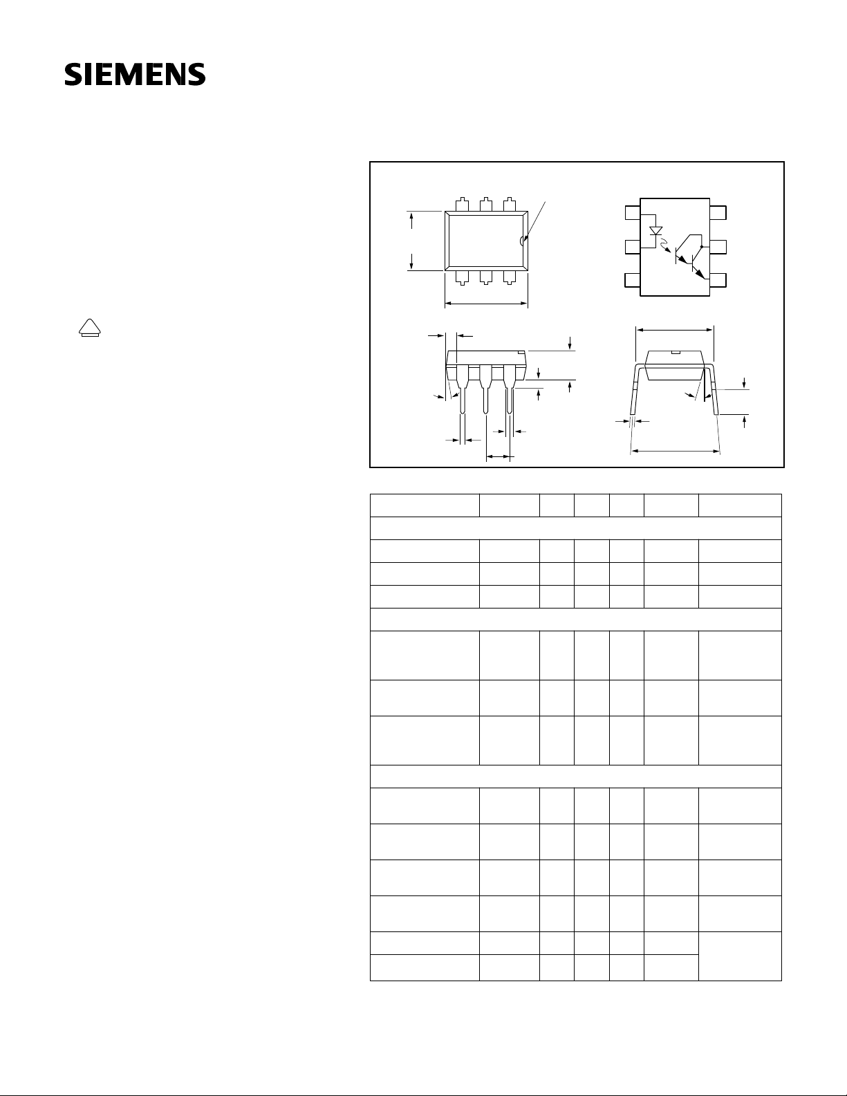
Package Dimensions in inches (mm)
Pin One ID.
3
.248 (6.30)
.256 (6.50)
4
.335 (8.50)
.343 (8.70)
.039
(1.00)
min.
4°
typ.
.018 (0.45)
.022 (0.55)
Electrical Characteristics
12
5
6
.130 (3.30)
.150 (3.81)
.020 (.051) min.
.031 (0.80)
.035 (0.90)
.100 (2.54) typ.
(T
=25 ° C)
A
Anode
Cathode
NC
1
2
3
.300 (7.62)
18° typ.
.010 (.25)
.014 (.35)
.300 (7.62)
.347 (8.82)
typ.
Base
6
Collector
5
Emitter
4
.110 (2.79)
.150 (3.81)
Parameter Symbol Min. Typ. Max. Unit Condition
Emitter
Forward Voltage V
Reverse Current I
Capacitance C
F
R
O
1.25 1.5 V I
0.1 10 µ AV
25 pF V
=20 mA
F
=3.0 V
R
=0
R
Detector
Collector-Emitter
Breakdown Volt-
BV
CEO
80 V I
=10 µ A
C
age
Collector-Emitter
Leakage Current
Emitter-Collector
Breakdown
I
CEO
V
ECO
25 1000 nA V
5.0 8.0 V I
CE
I
=0
F
=10 µ A
C
=60 V
Voltage
Package
Current Transfer
Ratio
Collector-Emitter
Saturation V oltage
Isolation Test
Voltage
CTR 500 % I
V
CEsat
VISO
0.9 1.0 V I
5300 VAC
RMS
=10 mA
F
V
=1.5 V
CE
=50 mA
C
I
=50 mA
F
1 sec., 60 Hz
Coupling
Capacitance C
Rise Time T
Fall Time T
ISOL
r
f
0.5 pF
10
35
µ sV
µ s
=13.5 V
CC
I
=50 mA
F
R
=100 Ω
L
5–219
V
gu e 6
V
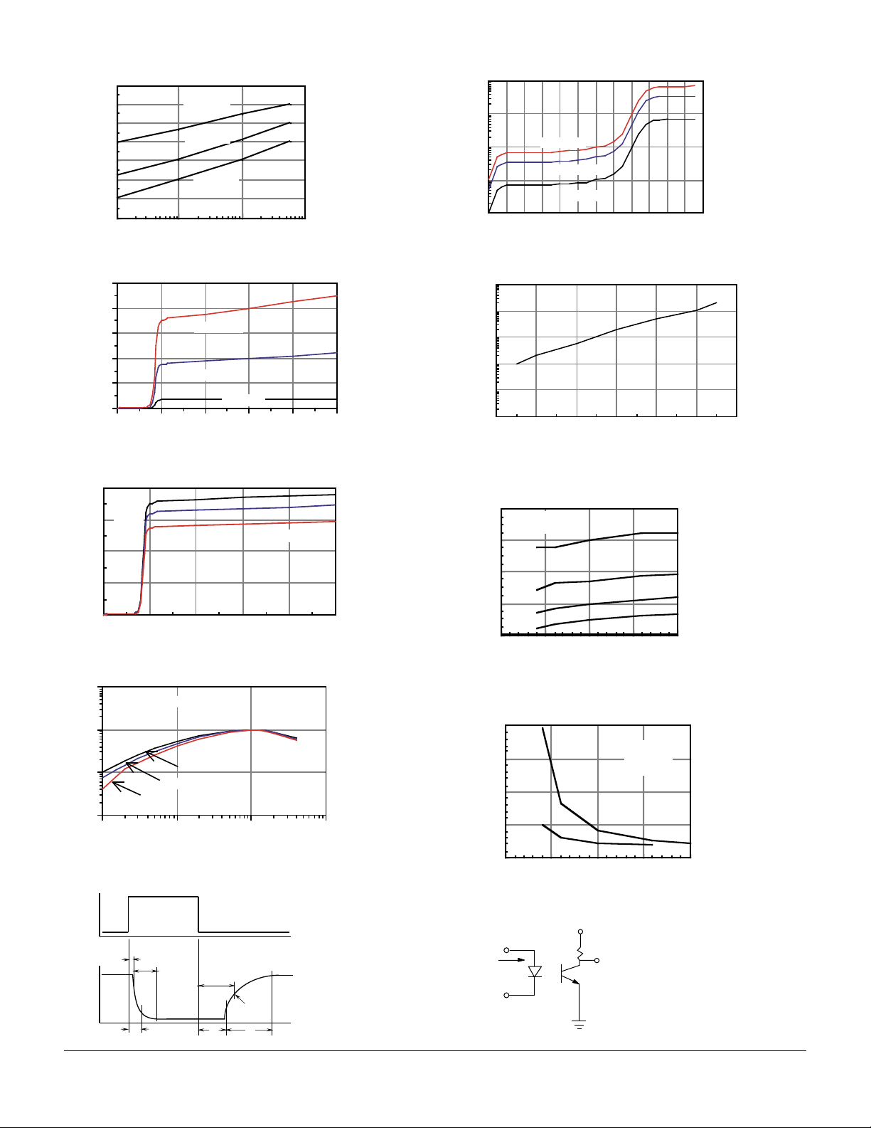
Figure 1. Forward voltage vs. forward current
1.4
1.3
1.2
1.1
1.0
0.9
0.8
VF - Forward Voltage - V
0.7
Ta = -55°C
Ta = 25°C
Ta = 85°C
100101.1
IF - Forward Current - mA
Figure 2. Typical Ic vs. Vce
100
80
60
IF=10 mA
40
20
Ic-Collector Current
0
IF=5 mA
IF=1 mA
Vce-Collector to Emitter Voltage
Figure 3. Typical Ic vs. Vce vs. temperature
8
25°C
50°C
6
75°C
4
2
Ic-Collector Current
0
Vce Collector-Emitter Voltage
Figure 4. Typical NCTR vs. LED current
10
Normalized @ 25°C
Vce=5V, IF=10 mA
1
NCTR
.1
25°C
50°C
75°C
.01
IF in mA
100101.1
Figure 9. Switching waveform
I
F
Figure 5. Typical Ic vs. Vce (sat. region)
100
10
1
.1
Ic-Collector Current
.01
IF=10 mA
IF=5 mA
IF=1 mA
1.21.00.80.60.40.20.0
Vce-Collector to Emitter Voltage
Figure 6. Typical Iceo vs. temperature
10000
1000
100
Iceo in nA
10
1
543210
.1
Temperature in °C
80706050403020
Figure 7. Low to high propagation delay vs. collector load
resistance and LED current
80
Ta = 25°C, Vcc = 5
Vth = 1.5 V
60
40
Delay - µs
20
543210
0
tpLH - Low/High Propagation
0 5 10 15 20
IF - LED Current - mA
1KΩ
220Ω
470Ω
100Ω
Figure 8. High to low propagation delay vs. collector load
resistance and LED current
20
15
10
delay - µs
5
0
tpHL - High/Low Propagation
0 5 101520
1KΩ
100Ω
IF - LED Current - mA
Ta = 25°C
Vcc = 5 V
Vth = 1.5
Figure 10. Switching schematic
V
= 5 V
CC
t
D
t
PHL
t
R
t
PLH
=1.5 V
V
TH
t
t
F
S
V
O
INPUT
5–220
R
L
V
OUT
MOC8050
 Loading...