

Siemens LH1550 Datasheet
LH1550
HIGH VOLTAGE, SOLID STATE RELAY
OPTOCOUPLER
FEATURES
• Normally Open, Single Pole Single Throw Operation
• Control 350 VAC or DC Voltage
• Switch 100 mA Loads
• LED Control Current, 2.5 mA
• Low ON-Resistance, 37 Ω Typ. at 100 mA
• Isolation T est V oltage, 3750 VA C
RMS
• Current Limit Protection
• Underwriters Lab File # E52744
APPLICATIONS
• Telephone Switch Hook
• High V oltage T est Equipment
• TRIAC Driver
• Motor Control
• Industrial Control Systems
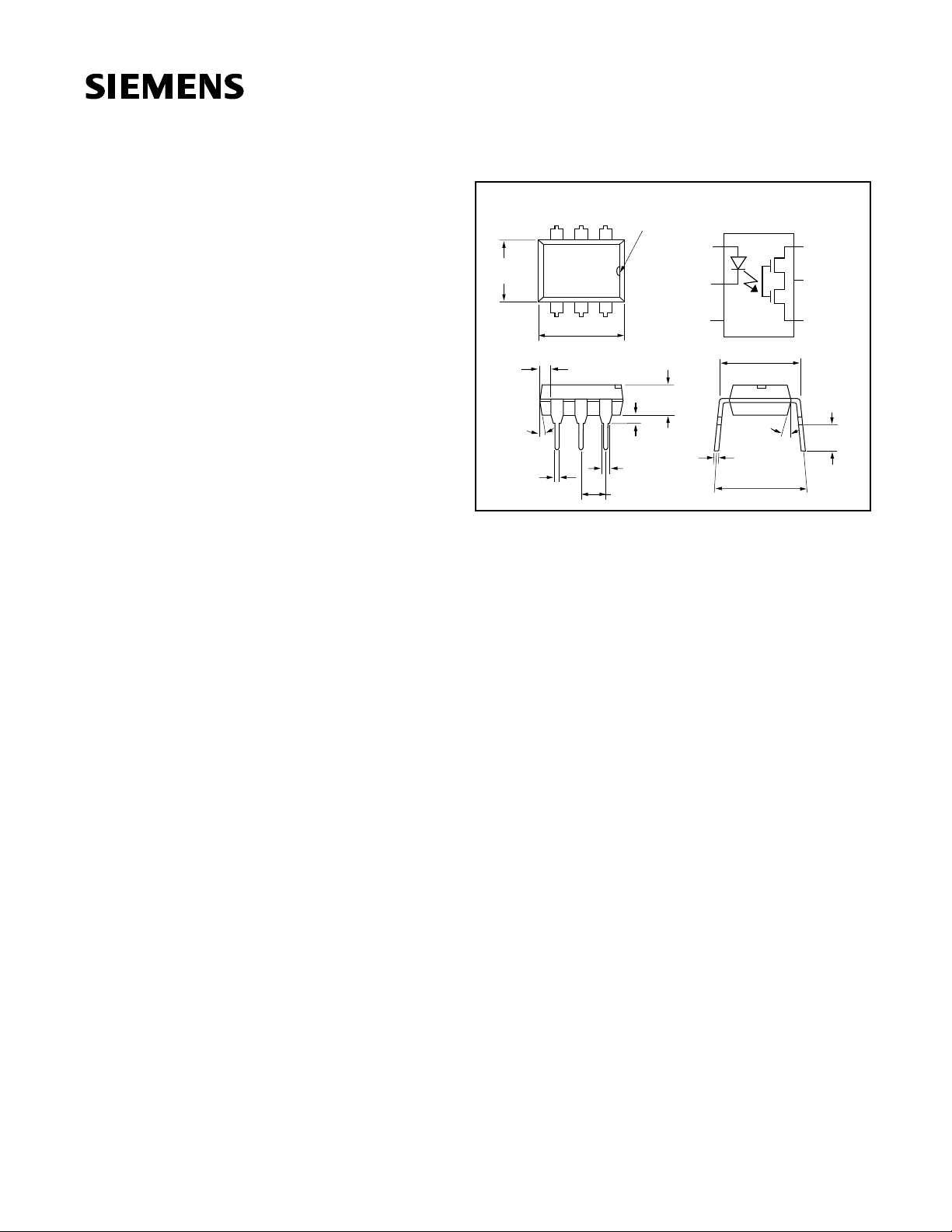
DESCRIPTION
The LH1550 is a single pole single throw (SPST), normally
open (NO), solid state relay. The relay can control AC or
DC loads currents up to 100 mA, with a supply voltage up
to 350 V. The device is packaged in a six pin 0.3 inch dualin line package. This package offers an insulation dielectric withstand of 3750 V
RMS
.
The coupler consists of a AlGaAs LED that is optically coupled to a dielectrically isolated photodiode array which
drives two series connected high voltage MOS transistors.
The typical ON-Resistance is 37 Ω
at 25 mA and is linear
up to 50 mA. There is built-in current limiting circuitry in the
detector chip, enabling it to pass FCC 68-302 and other
regulatory voltage surge requirements when over voltage
protection is provided.
Package Dimensions in Inches (mm)
Pin One ID.
12
5
6
.100 (2.54) Typ.
.130 (3.30)
.150 (3.81)
.020 (.051) Min.
.031 (0.80)
.035 (0.90)
NC
A
K
1
2
3
.300 (7.62)
.300 (7.62)
.347 (8.82)
Typ.
18° Typ.
.010 (.25)
.014 (.35)
6
S
5
NC
4
S'
.110 (2.79)
.150 (3.81)
.248 (6.30)
.256 (6.50)
.039
(1.00)
Min.
4°
Typ.
.018 (0.45)
.022 (0.55)
3
4
.335 (8.50)
.343 (8.70)
Absolute Maximum Ratings (T
Emitter
Reverse Voltage..................................................................5.0 V
Continuous Forward Current.............................................50 mA
Peak Forward Current (1 µ
Power Dissipation...........................................................100 mW
Derate Linearly from 25 °
C..........................................1.3 mW/ ° C
Detector
Output Breakdown Voltage.................................................350 V
Continous Load Current..................................................100 mA
Total Power Dissipation ..................................................300 mW
Derate Linearly from 25 °
C.......................................See Figure 4
Package
Isolation Test Voltage.............................................3750 VAC
Power Dissipation...........................................................400 mW
Derate Linearly from 25 °
C..........................................2.5 mW/ ° C
Isolation Resistance
V
=500 V, T
IO
V
=500 V, T
IO
=25 ° C.................................................... ≥ 10
A
=100 ° C................................................... ≥ 10
A
Storage Temperature Range................................–40 to +150 ° C
Operating Temperature Range...............................–40 to +85 °
Junction Temperature........................................................100 °
Soldering Temperature, 2 mm from case, 10 sec.............260 °
=25 ° C)
A
s) ..................................................1 A
RMS
12
Ω
11
Ω
C
C
C
5–208
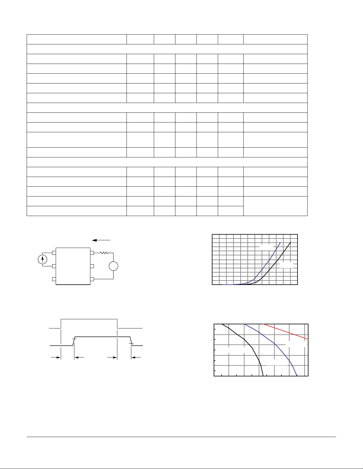
Characteristics (T
=25 ° C)
A
Description Symbol Min. Typ. Max. Unit Test Condition
Emitter
Forward Voltage V
Reverse Current I
Junction Capacitance C
Dynamic Resistance
Switching Time t
R
∆ V
R
F
J
/ ∆ I
F
, t
F
0.9 1.25 1.4 V I
110
15 pF V
F
6WI
1
=5 mA
F
AV
µ
µ
sI
=5 V
R
=0 V, f=1 MHz
F
=10 mA
F
=10 mA
F
Detector
Output Breakdown Voltage V
Output Off-State Leakage Current I
Feed through Capacitance, pins 4 to 6 C
Current Limit I
B
T(OFF)
T
LMT
350 380 V I
.03 1.0
µ AV
TBD I
150 190 270 mA I
=50 µ A
B
=
±
100 V, I
T
=0, f=1 KHz,
F
V
=4 VP-P
L
=5 mA, t=5 ms
F
Package
LED Forward Current for Turn-on I
LED Forward Current for Turn-off I
ON-resistance R
Turn-on Time t
Turn-off Time t
FON
FOFF
ON
ON
OFF
0.2 mA V
25 37 50 W I
0.8 3.0 ms I
0.04 3.0 ms
2.5 mA I
=100 mA, t=10 ms
L
= ± 300 V, I
L
=5 mA, I
F
=5 mA, V
F
R
=1 k Ω
L
=0 mA
F
=<5 µ A
L
=100 mA
L
=+50 V
L
Figure 1. Timing test circuit
1
I
F
2
3
6
5
4NC
Figure 2. Timing waveform
Control
Input
Switch
Output
90%
t
ON
NC
I
I
L
1 kΩ
F
Figure 3. LED forward current vs. forward voltage
120
100
85°C
80
+
50 V
–
60
40
25°C
20
0
1.81.61.41.21.00.80.6
IF Forward current in mA
tR≤1 µstR≤1 µs
Figure 4. Recommended load current vs. temperature
VF- Input LED forward Voltage
100
I
L
10%
t
OFF
80
60
IF=1.5 mA
40
20
0
IL-Load Current in mA
>4.5 mA
3.75 mA
806040200-20-40
Ambient temperature in °C
5–209
LH1550
 Loading...