

Siemens ILD32, ILQ32 Datasheet
.
.
)
)
Ω
DUAL CHANNEL
QUAD CHANNEL
ILD32
ILQ32
PHOTODARLINGTON OPTOCOUPLER
FEATURES
• Very High Current Transfer Ratio, 500% Min.
• Isolation T est V oltage, 5300 VA C
• High Isolation Resistance, 10
11
RMS
Typical
• Low Coupling Capacitance
• Standard Plastic DIP Package
• Underwriters Lab File #E52744
V
• VDE 0884 Available with Option 1
DE
Maximum Ratings (Each Channel)
Emitter
Peak Reverse Voltage........................................3 V
Continuous Forward Current.........................60 mA
Power Dissipation at 25 °
Derate Linearly from 25 °
C.........................100 mW
C....................1.33 mW/ ° C
Detector
Collector-Emitter Breakdown Voltage .............30 V
Collector (Load) Current..............................125 mA
Power Dissipation at 25 °
Derate Linearly from 25 °
C Ambient...........150 mW
C......................2.0 mW/ ° C
Package
Isolation Test V oltage (between emitter
and detector refer to standard climate
23 °
C/50%RH, DIN 50014)
t=1 sec...........................................5300 VAC
RMS
Creepage............................................... 7 mm min.
Clearance...............................................7 mm min.
Comparative Tracking Index per
DIN IEC 112/VDE303, part 1........................ ≥
Isolation Resistance
V
=500V, T
IO
V
=500V, T
IO
=25 ° C ......................... R
A
=100 ° C ....................... R
A
IO
IO
=10
=10
175
12
11
Total Dissipation at 25 ° C Ambient
ILD32 .....................................................400 mW
ILQ32 .....................................................500 mW
Derate Linearly from 25 °
C
ILD32 ...............................................5.33 mW/ °
ILQ32 ...............................................6.67 mW/ °
Storage Temperature ...................–55 °
Operating Temperature ...............–55 °
Lead Soldering Time at 260 °
C....................10 sec.
C to +150 ° C
C to +100 ° C
DESCRIPTION
The ILD32/ILQ32 are optically coupled isolators
with a Gallium Arsenide infrared LED and a silicon
photodarlington sensor . Switching can be achieved
while maintaining a high degree of isolation
between driving and load circuits. These optocouplers can be used to replace reed and mercury
relays with advantages of long life, high speed
switching and elimination of magnetic fields.
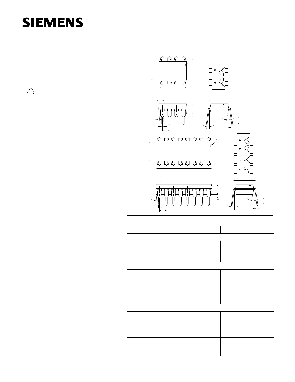
The ILD32 has two isolated channels in a DIP package, and the ILQ32 has four channels. These
devices can be used to replace 4N32s or 4N33s in
applications calling for several single channel optocouplers on a board.
Dimensions in inches (mm)
Dual
Channel
.268 (6.81)
.255 (6.48)
4°
Typ.
.022 (.56)
.018 (.46)
Quad
Channel
268 (6.81)
255 (6.48)
4°
Typ.
.022 (.56)
.018 (.46)
Ω
Ω
Electrical Characteristics (T
34
65
.390 (9.91)
.379 (9.63)
.045 (1.14)
.030 (.76)
.045 (1.14)
.030 (.76)
.100 (2.54)
.100 (2.54)
Typ.
Typ.
87
.150 (3.81)
.130 (3.30)
.790 (20.07)
.779 (19.77 )
=25 ° C)
A
Cathode
Cathode
.040 (1.02)
.030 (.76 )
Anode
Anode
1
2
3
4
.305 typ.
(7.75) typ.
3°–9°
Pin One I.D.
.150 (3.81)
.130 (3.30)
10°
Typ.
.012 (.30)
.008 (.20)
.040 (1.02)
.030 (.76 )
Pin One I.D.
12
Symbol Min. Typ. Max. Unit Condition
Emitter
Forward Voltage V
C
Reverse Current I
C
Capacitance C
F
R
O
1.25 1.5 V I
0.1 100 µ AV
25 pF V
Detector
Breakdown Voltage
Collector-Emitter
Breakdown Voltage
Emitter-Collector
Collector-Emitter
Leakage Current
BV
BV
I
CEO
CEO
ECO
30 V I
510 VI
1.0 100 nA V
Package
Current Transfer Ratio CTR 500 % I
Collector Emitter
Saturation Voltage
Isolation Capacitance C
Turn-On Time t
Turn-Off Time t
5–1
V
on
off
CEsat
ISOL
0.5 pF
15
30
8
Emitter
7
Collector
6
Collector
5
Emitter
.135 (3.43)
.115 (2.92)
Anode
1
Cathode
2
3
Cathode
4
Anode
5
Anode
6
Cathode
7
Cathode
8
Anode
.305 typ.
(7.75) typ.
10°
Typ.
3°–9°
.012 (.30)
.008 (.20)
1.0 V I
µ sV
µ sI
Emitter
16
Collector
15
14
Collector
13
Emitter
Emitter
12
Collector
11
10
Collector
9
Emitter
.135 (3.43
.115 (2.92
=10 mA
F
=3.0 V
R
=0 V
R
=100 µ A,
C
I
=0
F
=100 µ A
E
CE
I
=0
F
=10 mA
F
=2 mA,
C
I
=8 mA
F
CC
=5 mA,
F
R
=100 Ω
L
=10V,
=10 V
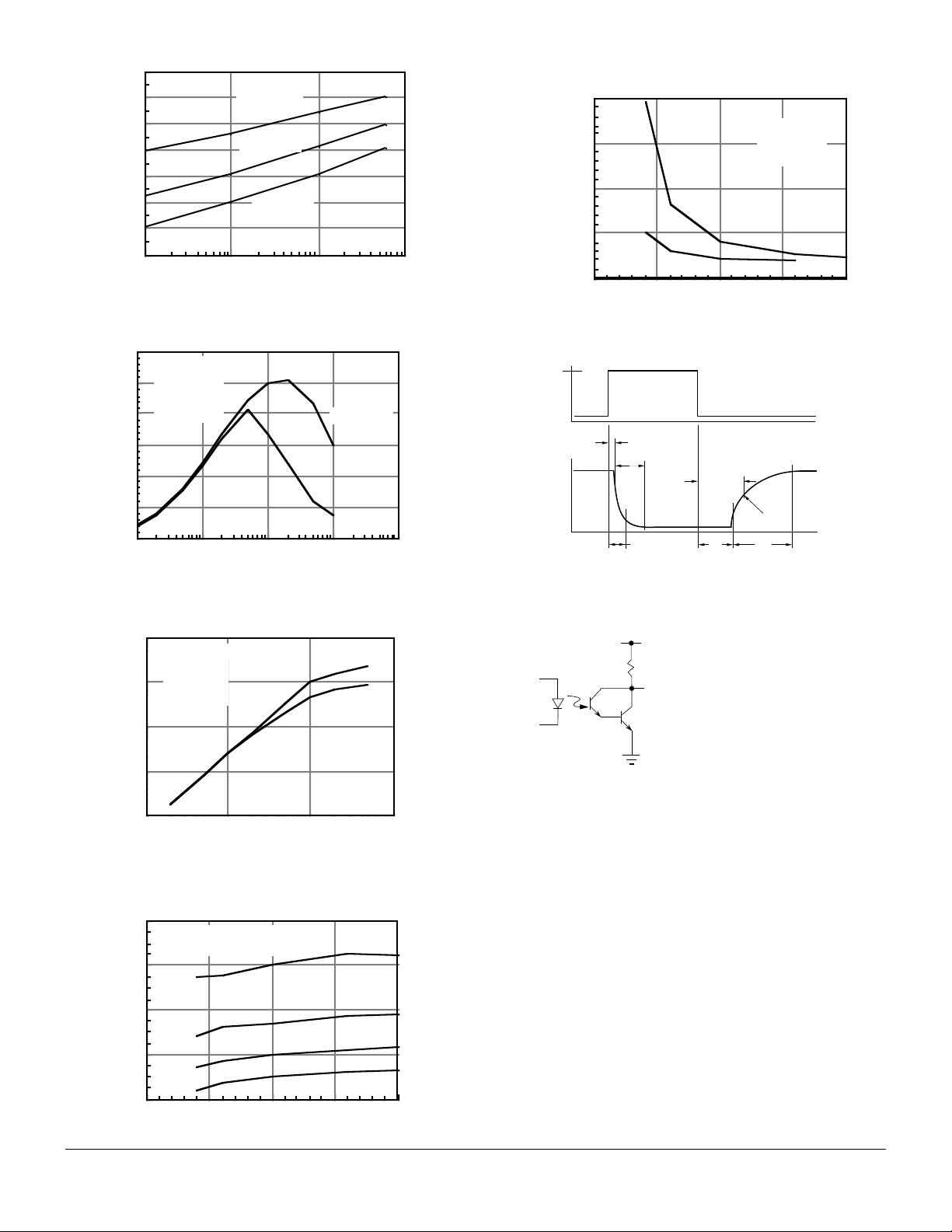
Figure 1. Forward voltage versus forward current
V
O
V
I
1.4
1.3
Ta = -55°C
1.2
1.1
Ta = 25°C
1.0
0.9
Ta = 85°C
0.8
VF - Forward Voltage - V
0.7
IF - Forward Current - mA
Figure 2. Normalized non-saturated and saturated
CTRce at TA=25 ° C versus LED current
1.2
Normalized to:
Vce = 10 V
1.0
IF = 10 mA
0.8
Ta = 25 °C
Vce = 10V
0.6
0.4
0.2
Vce =1V
0.0
NCTRce - Normalized CTR
.1 1 10 100 1000
IF - LED Current - mA
Figure 5. High to low propagation delay versus
collector load resistamce and LED current
20
15
10
dela y - µs
100101.1
tpHL - High/Low Propagation
100Ω
5
0
0 5 10 15 20
1KΩ
IF - LED Current - mA
Ta = 25°C
Vcc = 10 V
Vth = 1.5 V
Figure 6. Switching timing
I
F
t
D
t
O
R
t
PLH
VTH=1.5 V
t
PHL
t
t
S
F
Figure 3. Normalized non-saturated and saturated
collector-emitter current versus LED current
10
1
.1
.01
NIce - Normalized Ice
.001
Normalized to:
Ta = 25°C
IF = 10 mA
V ce = 10 V
IF - LE D Cur rent - mA
Vce = 10 V
V ce = 1V
101.1
100
Figure 4. Low to high propagation delay versus
collector load resistance and LED current
80
Ta = 2 5°C, Vcc = 10 V
Vth = 1.5 V
60
40
Dela y - µs
20
1K Ω
220 Ω
470 Ω
Figure 7. Switching schematic
VCC=10
F=10 KHz,
DF=50%
=5 mA
F
R
L
V
tpLH - Low/High Propagation
0
0 5 10 15 20
IF - LED Current - mA
100Ω
ILD32/ILQ32
5–2
 Loading...