

Siemens ILD255 Datasheet
.
.
)
)
DUAL CHANNEL
ILD255
BIDIRECTIONAL INPUT
OPTOCOUPLER
FEATURES
• AC or Polarity Insensitive Inputs
• Continuous Forward Current, 130 mA
• Applications—Telecommunications
- Ring Detection
- Loop Current Detector
• Built-in Reverse Polarity Input Protection
• Improved CTR Symmetry
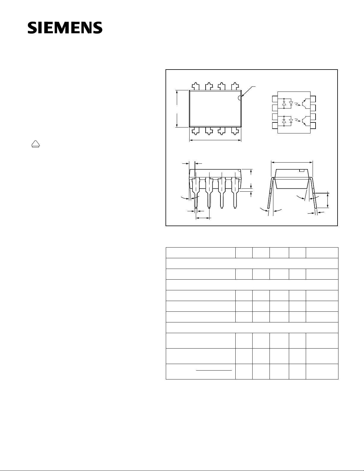
• Industry Standard DIP Package
• Underwriters Lab File #E52744
V
• VDE 0884 Available with Option 1
DE
DESCRIPTION
The ILD255 is a bidirectional input optically coupled isolator consisting of two high current Gallium
Arsenide infrared LEDs coupled to a silicon NPN
phototransistor per channel. The ILD255 has a
minimum CTR of 50%
These optocouplers are ideal for applications
requiring AC signal detection and monitoring.
Maximum Ratings (Each Channel)
Emitter
Peak Pulsed Current (1 µ s, 300 pps).................3 A
Continuous Forward Current...............130 mA RMS
Power Dissipation at 25 °
Derate Linearly from 25 °
C.........................175 mW
C..................... 2.3 mW/ ° C
Detector
Collector-Emitter Breakdown Voltage............. 30 V
Emitter-Base Breakdown Voltage..................... 5 V
Power Dissipation at 25 °
Derate Linearly from 25 °
C.........................200 mW
C..................... 2.6 mW/ ° C
Package
Isolation Test V oltage (between emitter
and detector referred to standard
climate 23 °
DIN 50014).....................................5300 VAC
C/50%RH,
RMS
Creepage................................................min. 7 mm
Clearance...............................................min. 7 mm
Isolation Resistance
V
=500 V, T
IO
V
=500 V, T
IO
Total Dissipation at 25 ° C............................ 400 mW
Derate Linearly from 25 °
Storage Temperature –55 °
Operating Temperature –55 °
Lead Soldering Time at 260 °
=25 ° C..........................R
A
=100 ° C........................R
A
C..................... 5.3 mW/ ° C
C .................. to +150 ° C
C ...............to +100 ° C
C ....................10 sec.
12
10
Ω
≥
IO
11
10
Ω
≥
IO
Dimensions in inches (mm)
268 (6.81)
255 (6.48)
4°
Typ.
.022 (.56)
.018 (.46)
34
65
.390 (9.91)
.379 (9.63)
.045 (1.14)
.030 (.76)
.100 (2.54)
12
87
Typ.
Cathode/
Cathode/
.150 (3.81)
.130 (3.30)
.040 (1.02)
.030 (.76 )
Pin One I.D.
Anode/
Cathode
Anode
Anode/
Cathode
Anode
1
2
3
4
.305 typ.
(7.75) typ.
10°
Typ.
3°–9°
.012 (.30)
.008 (.20)
8
Emitter
7
Collector
6
Collector
5
Emitter
.135 (3.43
.115 (2.92
Electrical Characteristics (T
Parameter MIn. Typ. Max. Unit Condition
Emitter
Forward Voltage V
Detector
BV
CEO
BV
ECO
I
CEO
Package
V
CEsat
DC Current Transfer Ratio 50 % I
Symmetry CTR at +10 mA
F
CTR at –10 mA
=25 ° C)
A
1.2 1.5 V I
30 50 V I
710 VI
550nAV
0.4 V I
0.50 1.0 2.0
= ± 10 mA
F
=10 mA
C
=10 µ A
E
CE
= ± 16 mA,
F
I
=2 mA
C
F
V
CE
=10 V
= ± 10mA,
=10 V
5–1
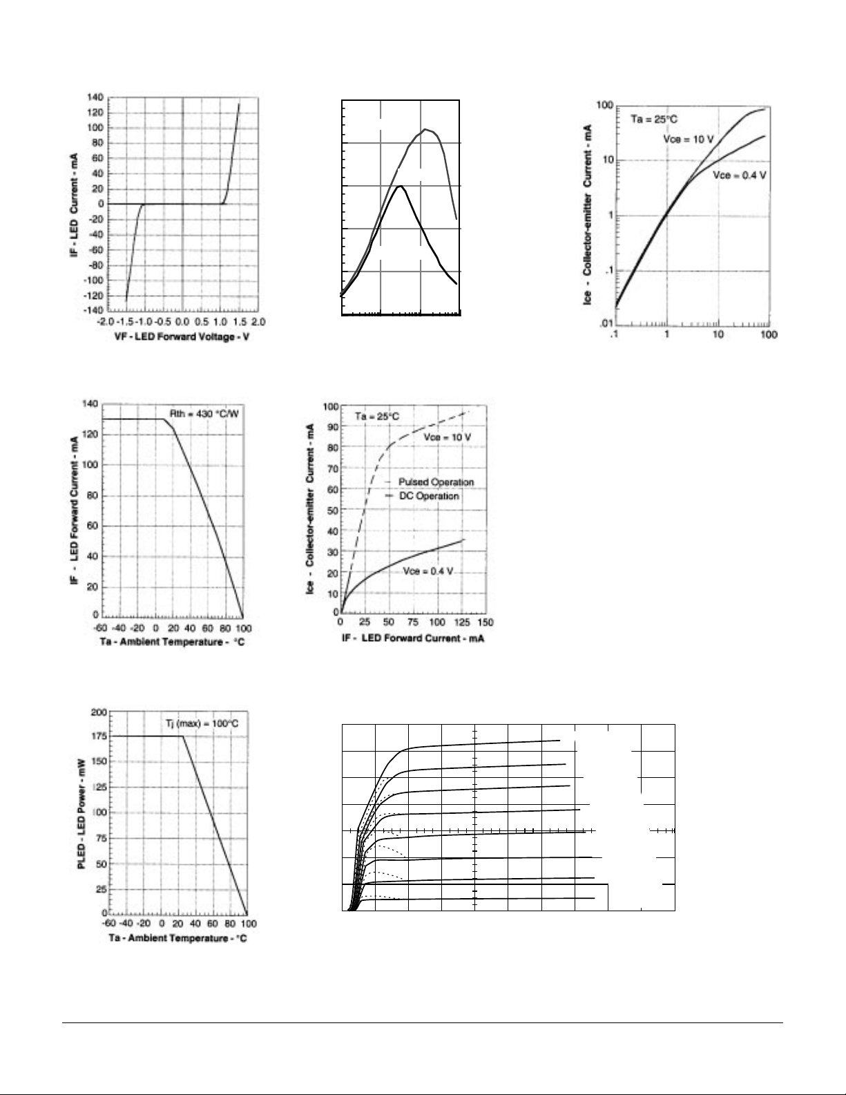
Figure 1. LED forward current versus forward voltage
Figure 2. Maximum LED current
versus ambient temperature
Figure 4. Current transfer ratio versus LED
current and collector-emitter voltage
250
Ta = 25°C
200
150
100
50
CTRce - Current Transfer Ratio - %
0
IF - LED Current - mA
Vce = 10V
Vce = 0.4V
100101.1
Figure 5. Saturated and nonsaturated collector-emitter current versus LED current
Figure 6. Saturated and nonsaturated collector-emitter current versus
LED current
Figure 3. Maximum LED power
dissipation
Figure 7. Collector emitter current versus collector emitter voltage
=8 mA
I
12
10
8
6
4
2
0
Ice–Collector Emitter Current – mA
0 0.2 0.4 0.6 1.0 1.4 1.8 2.2
F
=7 mA
I
F
I
F
I
=6 mA
=5 mA
F
=4 mA
I
F
=3 mA
I
F
=2 mA
I
F
I
F
=1 mA
Vce–Collector Emitter Voltage – V
5–2
ILD255
 Loading...