

Siemens IL755B Datasheet
)
)
.
.
Ω
IL755B
BIDIRECTIONAL INPUT
DARLINGTON OPTOCOUPLER
FEATURES
• Very High Current Transfer Ratio (500% min.)
IL755B-1: 750% at I
IL755B-2: 1000% at I
•BV
CEO
>60 V
• Isolation Test Voltage, 5300 VAC
2 mA, V
F=
=1 mA, V
F
CE
=5 V
CE
=5 V
RMS
• AC or Polarity Insensitive Inputs
• No Base Connection
• High Isolation Resistance, 10
12
• Low Coupling Capacitance
• Standard Plastic DIP Package
• Underwriters Lab Approval #E52744
• VDE #0884 Available with Option 1
DESCRIPTION
The IL755B is a bidirectional input, optically coupled isolator consisting of two Gallium Arsenide
infrared emitters and a silicon photodarlington sensor.
Maximum Ratings (at 25 ° C)
Emitter (Drive Circuit)
Continuous Forward Current.........................60 mA
Power Dissipation at 25 °
Derate Linearly from 55 °
C..........................100 mW
C....................1.33 mW/ ° C
Detector
Collector-Emitter Breakdown Voltage ..............60 V
Emitter-Collector Breakdown Voltage ..............12 V
Power Dissipation at 25 °
Derate Linearly from 25 °
C Ambient...........200 mW
C......................2.6 mW/ ° C
Package
Isolation Test V oltage
(PK), t=1 sec..................................5300 VAC
Dissipation at 25 ° C.....................................250 mW
Derate Linearly from 25 °
(2)
C
.................3.3 mW/ ° C
Creepage................................................ 7 min mm
Clearance................................................7 min mm
Isolation Resistance
T
=25 ° C.................................................. ≥ 10
A
T
=100 ° C................................................ ≥ 10
A
Storage Temperature
Operating Temperature ................–55 °
Lead Soldering Time at 260 °
(2)
..............–55 ° C to +150 ° C
C to +100 ° C
C....................10 sec.
12
11
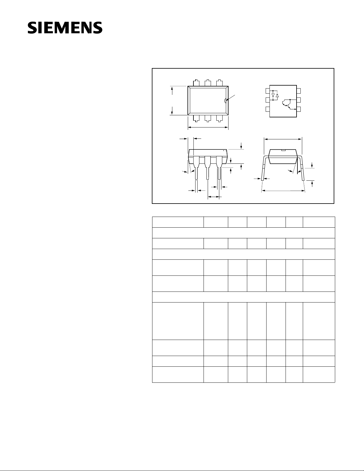
Dimensions in inches (mm)
248 (6.30)
256 (6.50)
4°
Typ.
.018 (0.45)
.022 (0.55)
Electrical Characteristics (T
Emitter
Forward Voltage
Detector
(2)
Breakdown Voltage,
Collector-Emitter
Leakage Current,
Collector-Emitter
Package
RMS
Current Transfer
(2)
Ratio
IL755B-1
IL755B-2
Ω
Ω
Saturation Voltage,
Collector-Emitter
Turn-On Time t
Turn-Off Time t
5
12
pin one
ID.
6
.130 (3.30)
.138 (3.50)
.032 (0.80)
Min.
.031 (0.80)
.035 (0.90)
.100 (2.54) Typ.
=25 ° C)
A
Anode/
Cathode
Catho e/
Anode
NC
1
2
3
.300 (7.62)
18° Typ.
.010 (.25)
.014 (.35)
.300 (7.62)
.347 (8.82)
Typ.
3
4
.335 (8.50)
.343 (8.70)
.039
(1.00)
Min.
Symbol Min. Typ. Max. Unit Condition
(1)
V
BV
I
CEO
F
CEO
60 75 V I
1.25 1.5 V I
1.0 100 nA V
CTR
V
on
off
CEsat
750
1000
1.0 V I
200 µ sV
200 µ sI
%
%
Base
6
Collector
5
Emitter
4
.114(2.90
.130 (3.30
=10 mA
F
=1 mA,
C
I
=0
F
=10 V,
CE
I
=0
F
I
= ± 2 mA,
F
V
=5 V
CE
I
= ± 1 mA,
F
V
=5 V
CE
=10 mA,
C
I
= ± 10 mA
F
=10 V
CC
=
±
2 mA,
F
R
=100 Ω
L
Notes:
1. Indicates JEDEC registered data.
5–1
V
C
C
V
C
C
0
V
V
C
V
A
V
V
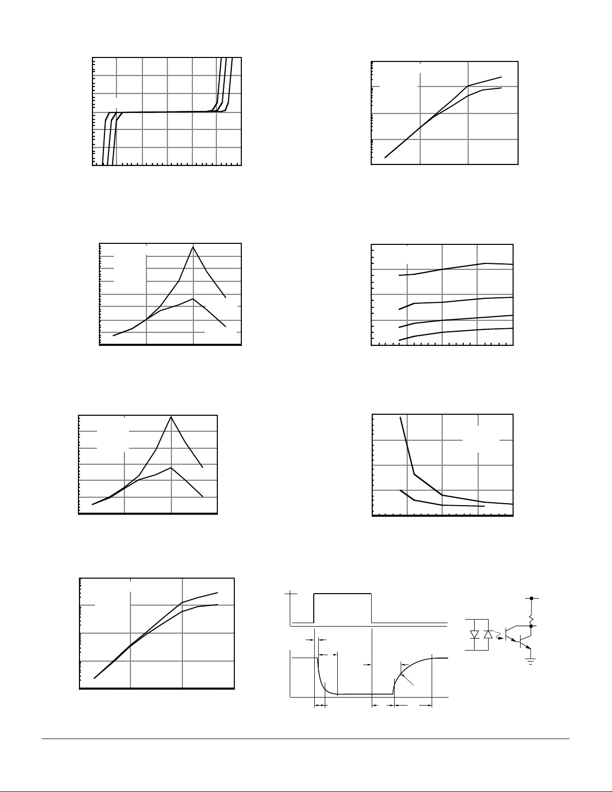
Figure 1. LED forward current versus forward voltage
60
40
20
25°
85°
0
–55°C
-20
-40
-60
-1.5 -1.0 -0.5 0.0 0.5 1.0 1.5
IF - LED Forward Current - mA
VF - LED Forward Voltage - V
Figure 2. Normalized non-saturated and saturated
CTRce versus LED current
4.0
Normalized to:
3.5
Ta = 25°
3.0
Vce = 5 V
IF = 1 mA
2.5
2.0
101.1
Vce = 5 V
Vce = 1
100
1.5
1.0
0.5
0.0
NCTRce - Normalized CTRce
IF - LED Current - mA
Figure 5. Normalized non-saturated and saturated
collector-emitter current versus LED current
10
Normalized to:
Ta = 25°C
IF = 10 mA
1
Vce = 5 V
.1
.01
NIce - Normalized Ice
.001
IF - LED Current - mA
Vce = 5
Vce = 1V
101.1
100
Figure 6. Low to high propagation delay versus
collector load resistance and LED current
80
Ta = 25°C, Vcc = 5
Vth = 1.5 V
60
40
Delay - µs
20
0
tpLH - Low/High Propagation
0 5 10 15 20
IF - LED Current - mA
1KΩ
220Ω
470Ω
100Ω
Figure 3. Normalized non-saturated and saturated
CTRce versus LED current
3.0
Normalized to:
2.5
2.0
1.5
1.0
0.5
0.0
NCTRce - Normalized CTRce
Ta = 25°
Vce = 5 V
IF = 2 mA
Vce = 5 V
Vce = 1 V
100101.1
IF - LED Current - mA
Figure 4. Normalized non-saturated and saturated
Ice versus LED current
10
Normalized to:
Ta = 25°
Vce = 5
10
IF = 2 m
1
.1
NIce - Normalized Ice
.01
IF - LED Current - mA
Vce = 5
Vce = 1
100101.1
Figure 7. High to low propagation delay versus
collector load resistance and LED current
20
15
10
delay - µs
5
0
tpHL - High/Low Propagation
0 5 10 15 20
1KΩ
100Ω
IF - LED Current - mA
Ta = 25°C
Vcc = 5 V
Vth = 1.5 V
Figure 8. Switching waveform Figure 9. Normalized non-satu-
rated and saturated CTRce versus LED current
I
F
F=10 KHz,
DF=50%
t
D
t
O
R
t
PLH
IF=2 mA
VCC=10 V
R
L
V
O
VTH=1.5 V
t
PHL
t
t
S
F
5–2
IL755B
 Loading...