

Siemens IL485 Datasheet
)
)
IL485
FEATURES
• Fast T urn On
• Fast T urn Off
• Low Input Current
• Isolation T est V oltage, 5300 VAC
RMS
APPLICA TIONS
• Motor Drive Controls
• IGBT-predrivers
• AC/DC Power Inverters
DESCRIPTION
The IL485 is a photovoltatic generator (optically coupled) designed to drive highly capacitive loads such
as the gate of a power MOSFET transistor and at the
same time provide isolation and floating voltage supply capability. The coupler consists of a GaAlAs light
emitting diode as input control and a custom photo IC
chip with photodiode arrary (PDA) as output device.
When the LED is turned on, the emitted light produces a voltage in the PDA. The output of the PDA is
used to drive the gate of a power MOSFET. The photo
IC chip contains additional circuitry to enhance the
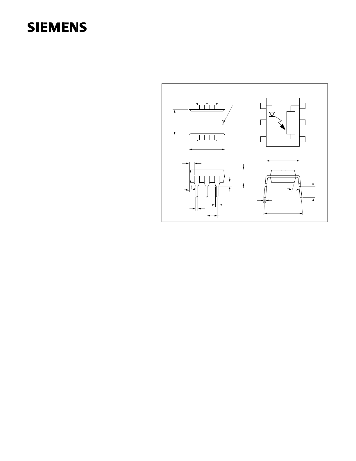
switching speeds, (both turn on turn off). The optocoupler is packaged in a 6 pin DIP.
OPTICALLY COUPLED
HIGH SPEED MOSFET DRIVERS
OPTOCOUPLER
Dimensions in inches (mm)
Pin One ID.
3
.248 (6.30)
.256 (6.50)
4
.335 (8.50)
.343 (8.70)
.039
(1.00)
Min.
4°
Typ.
.018 (0.45)
.022 (0.55)
12
5
6
.020 (.051) Min.
.100 (2.54) Typ.
.130 (3.30)
.150 (3.81)
.031 (0.80)
.035 (0.90)
Maximum Ratings
Emitter
Reverse Voltage ..................................................................................4 V
Forward Current ..............................................................................60 mA
Peak Forward Current....................................................................600 mA
Power Dissipation.........................................................................100 mW
Thermal Resistance....................................................................700 °
Detector
Breakdown Voltage (pin 5 to 6)........................................................300 V
Peak Input Current (pin 5 to 4)........................................................50 mA
Reverse Current (pin 5 to 6, V=100 V)...........................................200 nA
Power Dissipation (pin 5 to 4) ......................................................150 mW
Package
Insulation Thickness between Emitter and Detector................... ≥ 0.4 mm
Isolation Test Voltage (1 sec.)..............................................5300 VAC
Isolation Resistance
V
=500 V, T
IO
V
=500 V, T
IO
=25 ° C.................................................................. ≥ 10
A
=100 ° C............................................................... ≥ 10
A
Comparative Tracking Index per
DIN IEC 112/VDE 303, Part 1......................................................... ≥
Total Power Dissipation ................................................................250 mW
Storage Temperature Range..........................................–55 °
Operating Temperature Range.......................................–55 °
Junction Temperature......................................................................100 °
Soldering Temperature (max. 10 sec.,
dip soldering distance to seating plane >1.5 mm)......................260 °
A
K
1
2
3
18° Typ.
.300 (7.62)
Typ.
.010 (.25)
.014 (.35)
.300 (7.62)
.347 (8.82)
6
–out
5 B
4
+out
.110 (2.79
.150 (3.81
C/W
RMS
12
Ω
11
Ω
175
C to +150 ° C
C to +100 ° C
C
C
5–1

Electrical Characteristics
Parameter Symbol Min. Typ. Max. Unit Condition
Input — Emitter
LED Forward Voltage V
LED Junction Capacitance C
F
J
0.9 1.5 2.1 V I
25 pF V
=10 mA
F
=0 V, f=1 MHz
R
MOSFET Driver Output with External Biasing (see Figure 1 and Figure 3)
Zener Voltage (pin 4 to 6) V
Dynamic Output Voltage (pin 4 to 6) V
Dynamic Output Current (pin 4 to 6) I
Dynamic Output Resistance
Sourcing (pin 4)
Sinking (pin 4)
Turn-on Time t
Turn-off Time t
Z
OUT
OUT
R
OUT
ON
OFF
911 VC
13 V I
5
15
300
20
3.5 5
3.5 5
mA
mA
Ω
Ω
µ sC
µ sC
=10 µ A
ZT
=2000 pF, V
L
I
=10 mA
F
C
=2000 pF, V
L
I
=10 mA
F
I
=40 mA
F
I
=10 mA
F
=2000 pF, I
L
Measure at V
=2000 pF, I
L
Measure at V
MOSFET Driver Output without External Biasing (see Figure 2 and Figure 3)
Output Open Circuit Voltage (pin 4 to 6) V
Output Short Circuit Current (pin 4 to 6) I
Dynamic Output Resistance Sinking (pin 4) R
Turn-on Time t
Turn-off Time t
OC
SC
OUT
ON
OFF
710 VI
2.1
8.4
4
16
20
µ A
µ A
Ω
650 1000 µ sC
35
µ
sC
=10 mA
F
I
=10 mA
F
I
=40 mA
F
I
=10 mA
F
=2000 pF (see Figure 3)
L
Measure at V
=2000 pF (seeFigure 3)
L
Measure at V
MOSFET Driver Output Switching Speed (see Figure 3, Figure 4, Figure 5)
Rise time t
Turn-on Time t
Fall time t
Turn-off Time t
R
ON
F
OFF
500 ns
3.5
µ s
300 ns
3.5
µ s
M1 Cgs=2000 pF, V
Measure at 90%–10% M1 V
(see Figure 4)
Package Isolation Characteristics
Input-Output CMRR dv/dt 15 kV V/ µ sV
Coupling Capacitance C
IO
1 pF f=1 MHz
CM
=1000 V
=20 V
B
=20 V
B
=40 mA
F
OUT
=40 mA
F
OUT
OUT
OUT
=5 V, V
=2 V, V
=5 V, I
=2 V, I
=50 V
S
=20 V
B
=20 V
B
=40 mA
F
=40 mA
F
DS
5–2
IL485
 Loading...