

Siemens IL4108 Datasheet
IL4108
ZERO VOLTAGE CROSSING
800 V TRIAC DRIVER OPTOCOUPLER
FEATURES
• On-State Current, 300 mA
• Zero V oltage Crossing
• Blocking V oltage, 800 V
• Isolation T est V oltage 5300 VACRMS
• High Input Sensitivity
IFT=2 mA, PF=1.0
IFT=5 mA, PF ≤ 1.0
• High Static dv/dt 10,000 V/ µ s
• Inverse Parallel SCRs Provide Commutating
dv/dt >10K V/ µ s
• Very Low Leakage <10 µ A
• Small 6-Pin DIP Package
• Underwriters Lab File #E52744
• VDE Approval #0884 (Optional with Option 1,
Add -X001 Suffix)
Maximum Ratings
Emitter
Reverse Voltage .....................................................6 V
Forward Current ................................................60 mA
Surge Current.......................................................2.5 A
Thermal Resistance.......................................750 °
Derate from 25 °
C ......................................1.33 mW/ ° C
C/W
Detector
Peak Off-state Voltage.........................................800 V
Peak Reverse Voltage.........................................800 V
RMS On-state Current .....................................300 mA
Single Cycle Surge..................................................3 A
Thermal Resistance.......................................125 °
C/W
Total Power Dissipation...................................500 mW
Derate from 25 °
C ........................................6.6 mW/ ° C
Package
Isolation Test Voltage (between emitter
and detector, climate per DIN 40046,
part 2, Nov. 74 (t=1 min.)....................5300 VAC
RMS
Pollution Degree (DIN VDE 0109).............................. 2
Creepage Distance........................................... ≥
Clearance.......................................................... ≥
7 mm
7 mm
Comparative Tracking Index per DIN IEC
112/VDE 0303 part 1, Group IIIa per
DIN VDE 6110................................................... ≥
Isolation Resistance
V
=500 V, T
IO
V
=500 V, T
IO
=25 ° C .................................... ≥ 10
A
=100 ° C .................................. ≥ 10
A
175
12
11
Ω
Ω
Storage Temperature Range.............–55 ° C to +125 ° C
Ambient Temperature Range............–55 °
Soldering Temperature (max. ≤
dip soldering ≥
0.5 mm from
10 sec.
C to +100 ° C
case bottom)................................................... 260 °
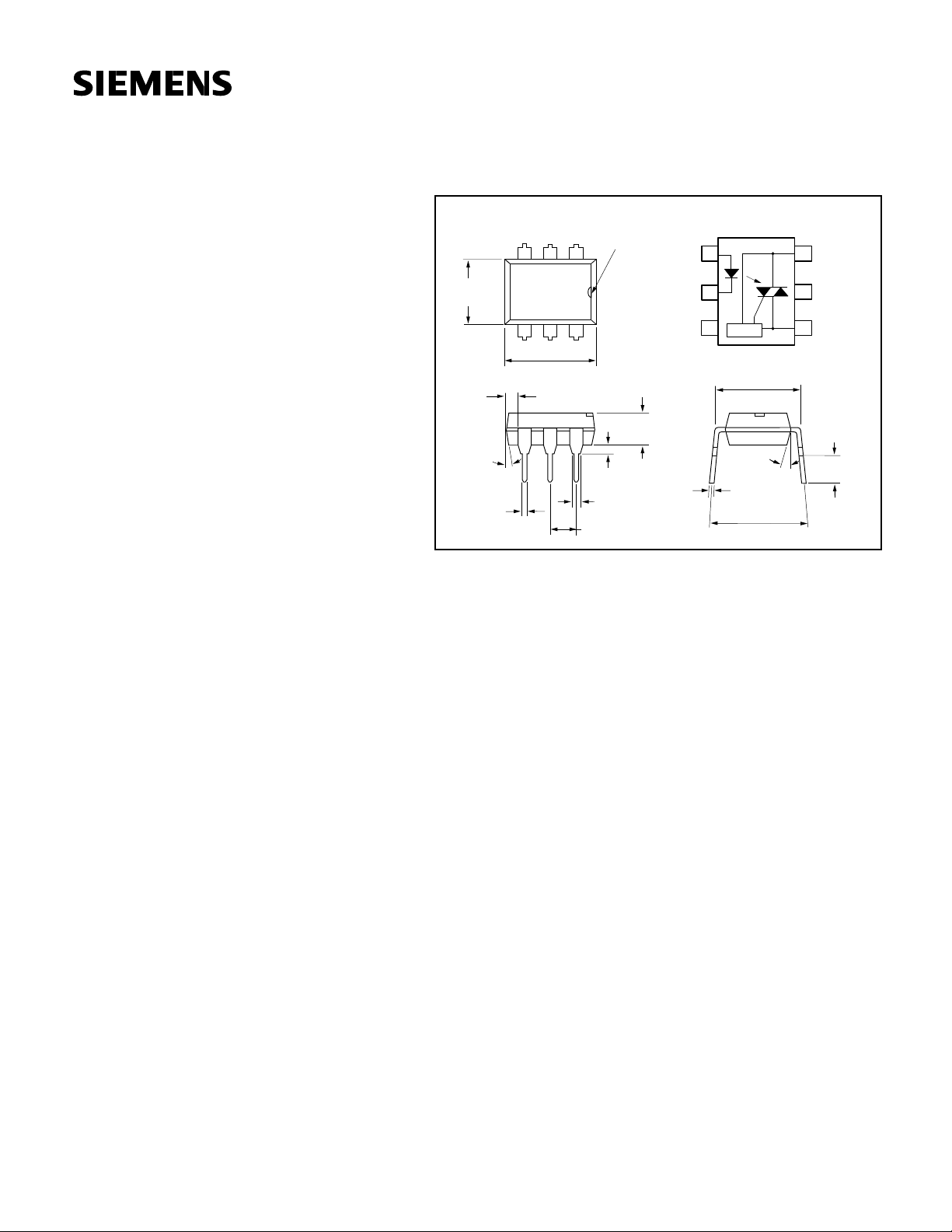
Package Dimensions in inches (mm)
.248 (6.30)
.256 (6.50)
.039
(1.00)
min.
4°
typ.
.018 (0.45)
.022 (0.55)
3
4
5
.335 (8.50)
.343 (8.70)
Pin One ID.
12
6
.130 (3.30)
.150 (3.81)
.020 (.051) min.
.031 (0.80)
.035 (0.90)
.100 (2.54) typ.
LED
Anode
LED
Cathode
NC
1
2
3
ZCC*
*Zero Crossing Circuit
.300 (7.62)
typ.
18° typ.
.010 (.25)
.014 (.35)
.300 (7.62)
.347 (8.82)
DESCRIPTION
The IL4108 consists of a GaAs IRLED optically coupled to a photosensitive zero crossing TRIAC network. The TRIAC consists of two inverse
parallel connected monolithic SCRs. These three semiconductors are
assembled in a six pin 0.3 inch dual in-line package, using high insulation double molded, over/under leadframe construction.
High input sensitivity is achieved by using an emitter follower phototransistor and a cascaded SCR predriver resulting in an LED trigger
current of less than 2 mA (DC).
The IL4108 uses two discrete SCRs resulting in a commutating dV/dt
greater than 10KV/ µ
static dV/dt of greater than 10KV/ µ
s. The use of a proprietary dv/dt clamp results in a
s. This clamp circuit has a MOSFET
that is enhanced when high dV/dt spikes occur between MT1 and MT2
of the TRIAC. When conducting, the FET clamps the base of the phototransistor, disabling the first stage SCR predriver.
The zero cross line voltage detection circuit consists of two enhancement MOSFETS and a photodiode. The inhibit voltage of the network is
determined by the enhancement voltage of the N-channel FET. The Pchannel FET is enabled by a photocurrent source that permits the FET
to conduct the main voltage to gate on the N-channel FET. Once the
main voltage can enable the N-channel, it clamps the base of the phototransistor, disabling the first stage SCR predriver.
The 800V blocking voltage permits control of off-line voltages up to
240VAC, with a safety factor of more than two, and is sufficient for as
much as 380VAC.
The IL4108 isolates low-voltage logic from 120, 240, and 380 VAC lines
to control resistive, inductive, or capacitive loads including motors, sole-
C
noids, high current thyristors or TRIAC and relays.
Applications include solid-state relays, industrial controls, office equip-
ment, and consumer appliances.
Triac
6
MT2
Substrate
5
do not
connect
Triac
4
MT1
.110 (2.79)
.150 (3.81)
5–141

Electrical Characteristics
Parameter Symbol Min. Typ. Max. Unit Condition
Emitter
Forward Voltage V
Breakdown Voltage V
Reverse Current I
Capacitance C
Thermal Resistance, Junction to Lead R
F
BR
R
0
THJL
630 V I
1.16 1.35 V I
0.1 10
µ AV
25 pF V
750
° C/W
=10 mA
F
=10 µ A
R
=6 V
R
=0 V, f=1 MHz
F
Output Detector
Repetitive Peak Off-state Voltage V
Off-state Voltage V
Off-state Current I
Off-state Current I
On-state Voltage V
On-state Current I
Surge (Non-repetitive On-state Current) I
Trigger Current 1 I
Trigger Current 2 I
Trigger Current Termperature Gradient
Inhibit Voltage Temperature Gradient
Off-state Current in Inhibit State I
Capacitance between Input and Output Circuit C
Holding Current I
Latching Current I
Zero Cross Inhibit Voltage V
Turn-on Time t
Turn-off Time t
DRM
D(RMS)
D(RMS)1
D(RMS)2
TM
TM
TSM
FT1
FT2
I
∆
FT1
∆
I
FT2
V
∆
DINH
∆
T
j
DINH
IO
H
L
IH
ON
OFF
Critical Rate of Rise of Off-State Voltage dv/dt
dv/dt
Critical Rate of Rise of Voltage at
Current Commutation
dv/dt
dv/dt
Critical Rate of Rise of On-state Current di/dt/
Thermal Resistance, Junction to Lead R
THJL
cr
cr
crq
crq
cr
800 V I
565 V I
10 100 µ AV
200 µ AV
1.7 3 V I
300 mA PF=1.0, V
3 A f=50 Hz
2.0 mA V
6.0 mA V
/
T
∆
j
∆
/
T
j
/
7
7
14
14
–20 mV/K
50 200 µ AI
2.0 pF V
65 500 µ A
5mAV
15 25 V I
35
50
10000
5000
10000
5000
8A/µs
150 °C/W
=100 µ A
DRM
D(RMS)
=800 V, T
D
mA
=800 V, I
D
=300 mA
T
=5 V
D
=220 V, f=50 Hz,
op
T
=100 ° C, t
j
µ A/K
µ A/K
=I
F
FT1
=0, f=1 kHz
D
=2.2 V
T
=Rated I
F
µ sV
RM
=V
µ s PF=1.0, I
V/ µ s
V/
µ s
V/µs
V/µs
=0.67 V
V
D
T
=80°C
j
V
=0.67 V
D
di/dt
T
=25°C
j
T
=80°C
j
crq
Package
Critical Rate of Rise of Coupled Input/Output
Voltage
Common Mode Coupling Capacitor C
Package Capacitance C
dv
/dt 1000
(IO)
CM
IO
0
0.01 pF
0.8 pF f=1 MHz, VIO=0 V
V/µsI
=0 A,
T
V
RM=VDM
=70 µ A
F
T(RMS)
pF
, V
DRM
FT
=565 VAC
DM
=300 mA
T
DRM
DRM
<15 A/ms
=565 VAC
100 ° C, I
A
=Rated I
=1.7 V
>10 ms
, Tj=25°C
,
=0
F
FT
5–142
IL4108
 Loading...