

Siemens BF2040W Datasheet
BF 2040W
Semiconductor Group
Jun-05-19981
Silicon N-Channel MOSFET Tetrode
Preliminary data
• For low noise, high gain controlled
input stages up to 1GHz
• Operating voltage 5V
ESD: Electrostatic discharge sensitive device, observe handling precaution
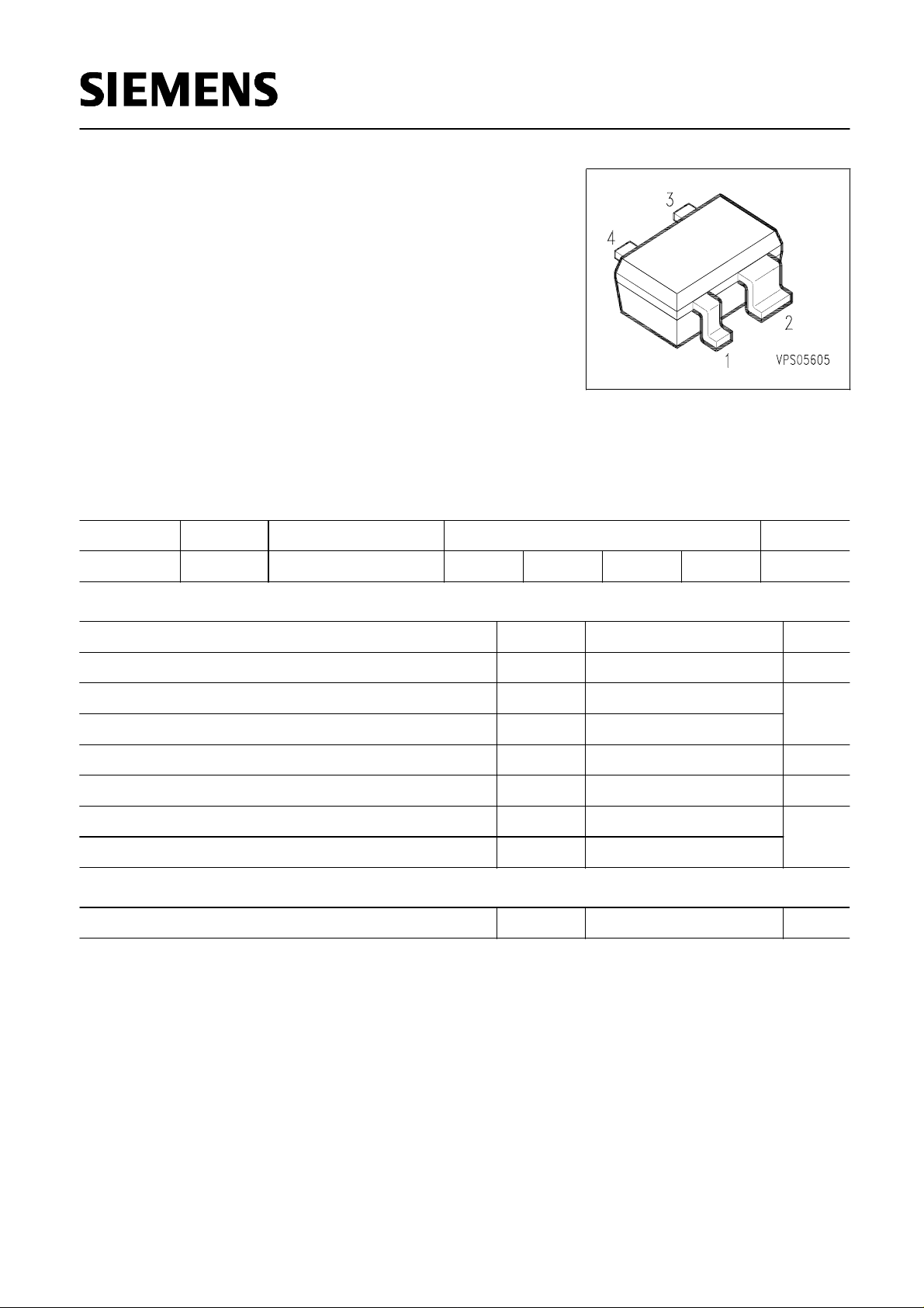
Type Marking Ordering Code Pin Configuration Package
BF 2040W NCs Q62702-F1776 1 = D 2 = S 3 = G1 4 = G2 SOT-343
Maximum Ratings
Unit
Parameter ValueSymbol
Drain-source voltage
V
DS
V14
40 mAContinuos drain current
I
D
Gate 1/gate 2 peak source current ±
I
G1/2SM
10
Gate 1 (external biasing) +
V
G1SE
7 V
200 mWTotal power dissipation,
T
S
= 94 °C
P
tot
Storage temperature
T
stg
°C-55 ...+150
Channel temperature
T
ch
150
Thermal Resistance
Channel - soldering point
≤280 K/W
R
thchs
Semiconductor Group 1 1998-11-01
BF 2040W
Semiconductor Group
Jun-05-19982
Electrical Characteristics at
T
A
= 25°C, unless otherwise specified.
Parameter
Symbol Values Unit
min. typ. max.
DC characteristics
Drain-source breakdown voltage
I
D
= 650 µA, -
V
G1S
= 4 V, -
V
G2S
= 4 V
V
(BR)DS
- - V12
Gate 1 - source breakdown voltage
+
I
G1S
= 10 mA,
V
G2S
= 0 V,
V
DS
= 0 V
+
V
(BR)G1SS
- -8.5
Gate 2 - source breakdown voltage
±
I
G2S
= 10 mA,
V
G1S
=
V
DS
= 0
- -+
V
(BR)G2SS
8.5
Gate 1 source current
V
G1S
= 5 V,
V
G2S
= 0 V
50+
I
G1SS
- nA-
50Gate 2 source leakage current
V
G2S
= 5 V,
V
G1S
= 0 V,
V
DS
= 0 V
- -+
I
G2SS
Drain current
V
DS
= 5 V,
V
G1S
= 0 V,
V
G2S
= 4 V
- - µA
I
DSS
-
Drain-source current
V
DS
= 5 V,
V
G2S
= 4 V,
R
G1
= 40 kΩ
15 mA- -
I
DSX
V
V
G2S(p)
Gate 2-source pinch-off voltage
V
DS
= 5 V,
I
D
= 20 µA
-0.60.3
0.3 0.7 -Gate 1-source pinch-off voltage
V
DS
= 5 V,
V
G2S
= 4 V,
I
D
= 20 µA
V
G1S(p)
AC characteristics
Forward transconductance
V
DS
= 5 V,
I
D
= 15 mA,
V
G2S
= 4 V
g
fs
45- - mS
3.7 -Gate 1 input capacitance
V
DS
= 5 V,
I
D
= 15 mA,
V
G2S
= 4 V,
f
= 1 MHz
C
g1ss
- pF
2.3 --
C
dss
Output capacitance
V
DS
= 5 V,
I
D
= 15 mA,
V
G2S
= 4 V,
f
= 1 MHz
Noise figure
V
DS
= 5 V,
I
D
= 15 mA, f = 800 MHz
F
- 2 - dB
Semiconductor Group 2 1998-11-01
 Loading...