

BCP 51M ... BCP 53M
1
Semiconductor Group
Au -11-1998
PNP Silicon AF Transistor
• For AF driver and output stages
• High collector current
• Low collector-emitter saturation voltage
• Complementary types: BCP 54M...BCP 56M(NPN)
VPW05980
1
2
3
5
4
Type Marking Ordering Code Pin Configuration Package
SCT-5952 = C 5 = C3 = E1 = BBCP 51M
BCP 52M
BCP 53M
AAs
AEs
AHs
Q62702-C2592
Q62702-C2593
Q62702-C2594
4 n.c.
Maximum Ratings
Parameter
Symbol BCP 53M UnitBCP 52MBCP 51M
V45
V
CEO
60 80Collector-emitter voltage
V
CBO
45 100Collector-base voltage 60
5
V
EBO
5Emitter-base voltage 5
mADC collector current
I
C
1
Peak collector current
I
CM
A1.5
100 mABase current
I
B
Peak base current 200
I
BM
P
tot
1.7 W
Total power dissipation,
T
S
≤ 77 °C
°C150Junction temperature
T
j
Storage temperature
T
stg
-65...+150
Thermal Resistance
R
thJA
≤98
Junction ambient
1)
K/W
Junction - soldering point
R
thJS
≤43
1) Package mounted on pcb 40mm x 40mm x 1.5mm / 6cm2 Cu
Semiconductor Group 1 1998-11-01
BCP 51M ... BCP 53M
2
Semiconductor Group
Au -11-1998
Electrical Characteristics at
T
A
= 25°C, unless otherwise specified.
Symbol
Values UnitParameter
min. max.typ.
DC Characteristics
-
-
-
-
-
-
V
45
60
80
V
(BR)CEO
BCP 51M
BCP 52M
BCP 53M
Collector-emitter breakdown voltage
I
C
= 10 mA,
I
B
= 0
45
60
100
-
-
-
BCP 51M
BCP 52M
BCP 53M
-
-
-
V
(BR)CBO
Collector-base breakdown voltage
I
C
= 100 µA,
I
B
= 0
V
(BR)EBO
5Emitter-base breakdown voltage
I
E
= 10 µA,
I
C
= 0
- -
nA100Collector cutoff current
V
CB
= 30 V,
I
E
= 0
-
I
CBO
-
µA- 20-Collector cutoff current
V
CB
= 30 V,
I
E
= 0 ,
T
A
= 150 °C
I
CBO
- -25 -
h
FE
DC current gain 1)
I
C
= 5 mA,
V
CE
= 2 V
250
h
FE
-40DC current gain 1)
I
C
= 150 mA,
V
CE
= 2 V
- -
h
FE
25DC current gain 1)
I
C
= 500 mA,
V
CE
= 2 V
0.5-
V
CEsat
Collector-emitter saturation voltage1)
I
C
= 500 mA,
I
B
= 50 mA
- V
1Base-emitter voltage 1)
I
C
= 500 mA,
V
CE
= 2 V
V
BE(ON)
- -
AC Characteristics
f
T
- 100 - MHzTransition frequency
I
C
= 50 mA,
V
CE
= 10 V, f = 100 MHz
1) Pulse test: t ≤ 300µs, D = 2%
Semiconductor Group 2 1998-11-01

BCP 51M ... BCP 53M
3
Semiconductor Group
Au -11-1998
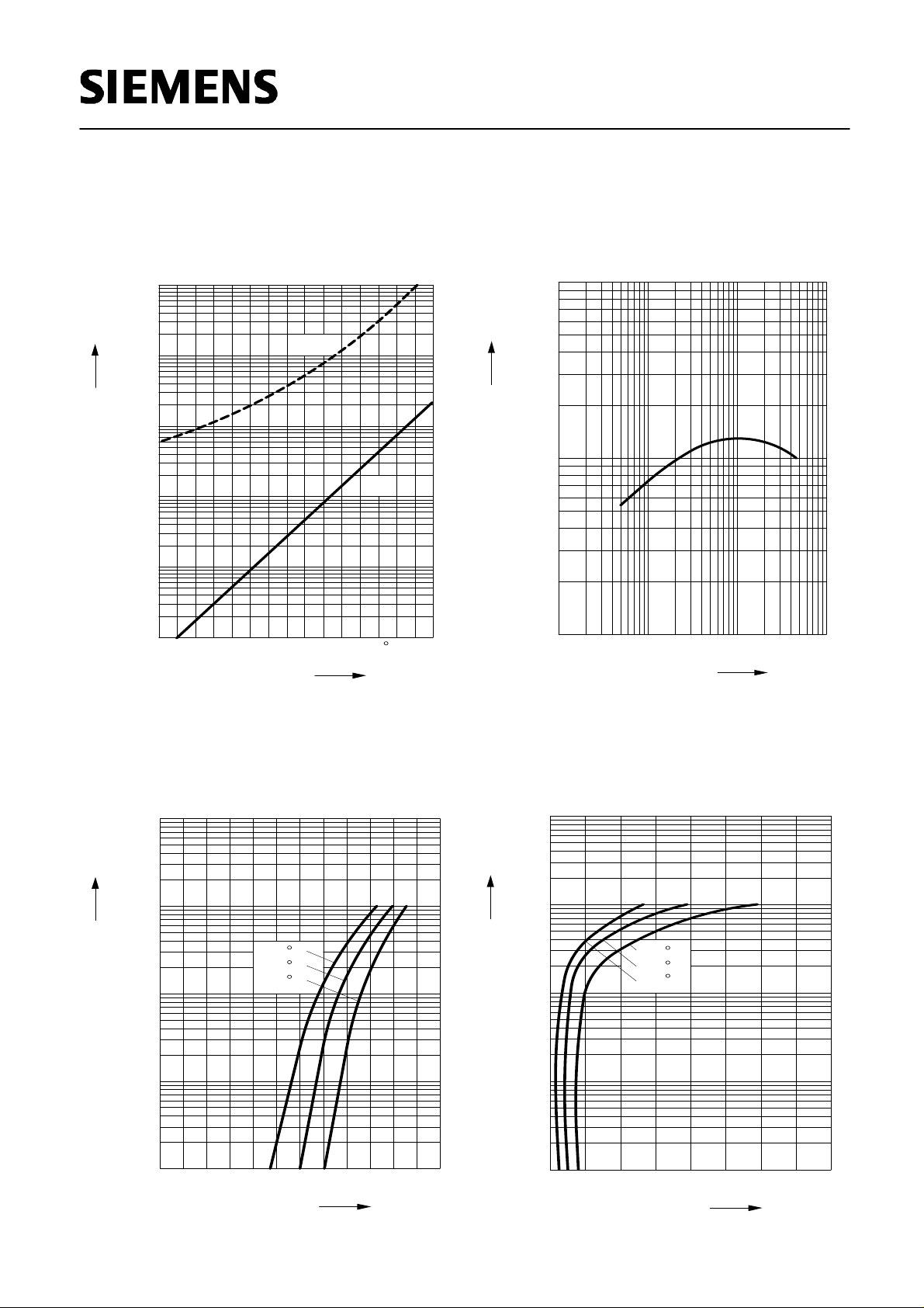
DC current gain
h
FE
= f (
I
C
)
V
CE
= 2V
10
EHP00261BCP 51...53
04
10mA
0
10
3
10
5
5
10
1
10
2
10
1
C
FE
h
Ι
3
10
2
10
C
100
5
25
C
-50
C
Total power dissipation
P
tot
= f (
T
A
*;
T
S
)
* Package mounted on epoxy
0 20 40 60 80 100 120
°C
150
TA,T
S
0
200
400
600
800
1000
1200
1400
1600
mW
2000
P
tot
T
S
T
A
Permissible Pulse Load
P
totmax
/
P
totDC
= f (
t
p
)
10
-6
10
-5
10
-4
10
-3
10
-2
10
0
s
t
p
0
10
1
10
2
10
3
10
-
P
totmax
/ P
totDC
D = 0
0.005
0.01
0.02
0.05
0.1
0.2
0.5
Permissible Pulse Load
R
thJS
= f (
t
p
)
10
-6
10
-5
10
-4
10
-3
10
-2
10
0
s
T
S
-1
10
0
10
1
10
2
10
K/W
R
thJS
0.5
0.2
0.1
0.05
0.02
0.01
0.005
D = 0
Semiconductor Group 3 1998-11-01
BCP 51M ... BCP 53M
4
Semiconductor Group
Au -11-1998
Collector cutoff current
I
CBO
= f (
T
A
)
V
CB
= 30V
0
10
EHP00262BCP 51...53
A
T
150
-1
4
10
Ι
CBO
nA
50 100
0
10
1
10
3
10
C
10
2
max
typ
Transition frequency
f
T
= f (
I
C
)
V
CE
= 10 V
10
EHP00260BCP 51...53
03
10mA
1
10
3
10
5
5
10
1
10
2
10
2
C
T
f
MHz
Ι
Base-emitter saturation voltage
I
C
= f (
V
BEsat
),
h
FE
= 10
0
10
EHP00263BCP 51...53
BEsat
V
0
4
10
Ι
C
mA
0.2
1
10
2
10
3
10
0.4 0.6 0.8 1.2V
C
100
25
C
-50
C
Collector-emitter saturation voltage
I
C
= f (
V
CEsat
),
h
FE
= 10
0
10
EHP00264BCP 51...53
CEsat
V
0.4 V 0.8
0
10
1
10
2
4
10
5
5
Ι
C
mA
5
3
10
0.2 0.6
C
100
25
C
C
-50
Semiconductor Group 4 1998-11-01
 Loading...