

Sherwood S-9500B Service Manual
MODEL
S.95OOb
ALL-SILICON
SOLID.STATE
STEREO
AMPLIFIER
SERVICE
MANUAL
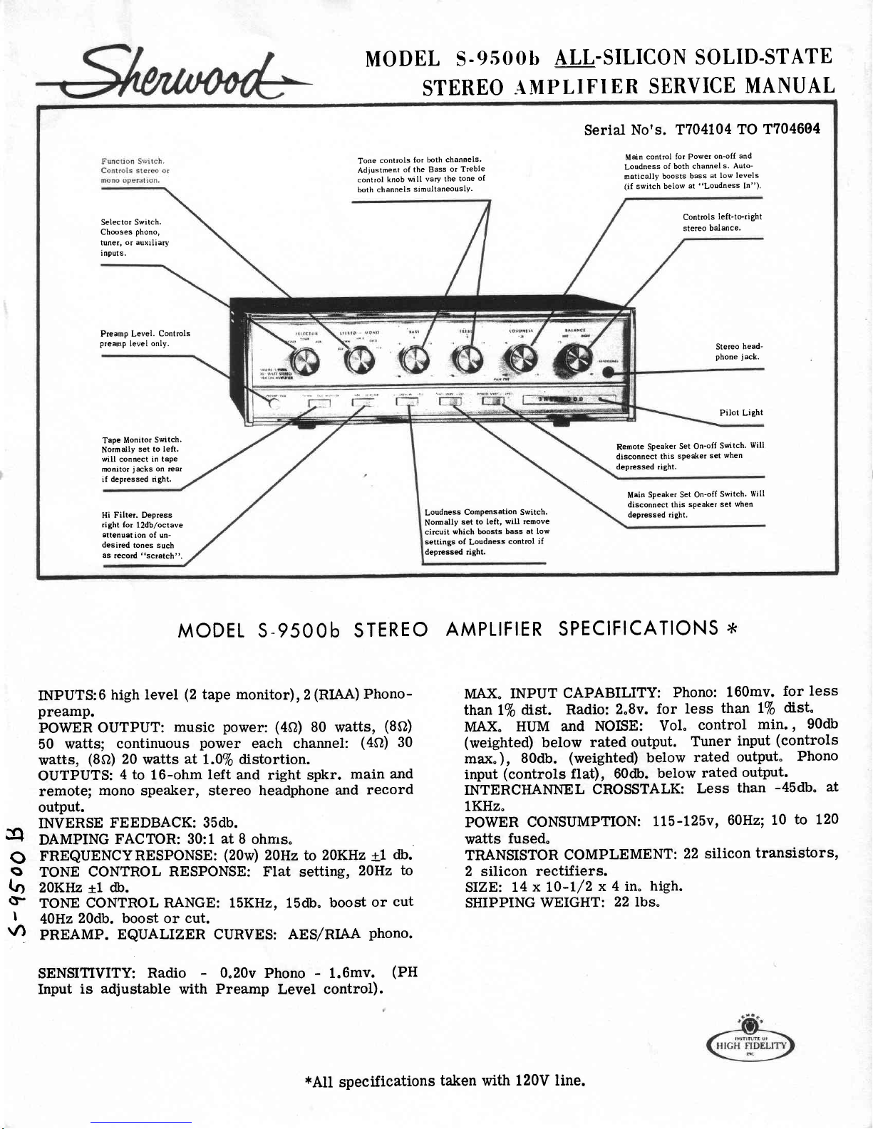
Tone
controls
for
both
channels.
Adjustment
of the Bass
or
Treble
control
knob
will vary the
tone
of
both channels
simultaneouslY.
Serial
No's. T704104
TO T704604
Main
control for Power
on-off
and
Loudness
of both channel
s. Auto-
matically
boosts
bass
at low
levels
(if
switch below
at
"Loudness
In").
Controls
left-to-right
stereo balance.
Stereo
head-
phone
jack.
Pilot Light
Remote
Speaker
Set On-off
Switch.
Will
disconnect
this
speaker
set
when
depressed right.
Main
Speaker Set On-off
Switch'
Will
disconnect this
speaker
set
when
depressed right.
Selector
Switch.
Chooses
phono,
tuner,
or auxrliary
i
nput
s.
Preamp
Level. Controls
preamp
level
only.
Tape
Monitor
Switch'
Normally
set to left.
will
connect
in tape
monitor
jacks
on rear
if depressed right,
Hi
Filter. Depress
right for
l2dbloctave
attenuat
ion of un-
desired
tones such
as
tecond
"scratch',,
Loudness
Compensetion Switch.
Normally
set to
left,
will remove
circuit
which boosts
bass
at low
settings of
Loudness
control if
depressed right.
MODEL
S.95OOb STEREO
AMPLIFIER SPECIFICATIONS
{<
rq
o
o
Io
$'
t
V)
INPUTS:6
high level
(2
tape monitor),
2
(RIAA)
Phonopreamp.
POWER
OUTPUT:
music
power: (4O)
80 watts,
(8O)
50
watts;
continuous
power
each channel:
(4O)
30
watts,
(8Ct)
20
watts
at
l.D%o distortion.
OUTPUTS:
4 to 16-ohm
left
and right
spkr.
main
and
remote;
mono speaker, stereo headphone
and
record
output.
INVERSE
FEEDBACK: 35db.
DAMPING
FACTOR: 30:1
at
8
ohrrs"
FREQUENCYRESPONSE:
(20w)
20Hz
to
20KHz
+1
db.
TONE
CONTROL RESPONSE:
Flat
setting,
20Hz
to
z0K.llz
11
db.
TONE
CONTROL RANGE: 15KHz,
15db.
boost
or
cut
40Hz
20db.
boost
or
cut.
PREAMP.
EQUALIZER CURVES: AES/RIAA
phono.
SENSITIVITY:
Radio - 0.20v
Phono - 1.6mv.
(PH
Input
is
adjustable
with
Preamp
Level
control).
MAX" INPUT
CAPABILITY:
Phono:
160mv.
for
less
than 170
dist.
Radio:
2.8v.
for less
than LVo
dist"
MAX. HUM
and
NOISE:
Vol.
control
min.
,
90db
(weighted)
betow
rated output.
Tuner
input
(controls
max"),
80db.
(weighted)
below
rated
output.
Phono
input
(controls
flat),
60db.
below
rated
output.
INTERCHANNEL
CROSSTALK:
Less
than
-45db"
at
1KHz"
POWER
CONSUMPTION:
115-125v,
6QHz;10
to L20
watts
fused.
TRANSISTOR
COMPLEMENT:
22 silicon
transistors,
2 silicon
rectifiers.
SIZE:
14 x L0-l/2
x 4 in"
high.
SHIPPING
WEIGHT:
22 lbs"
*All
specifications
taken with
120V line.
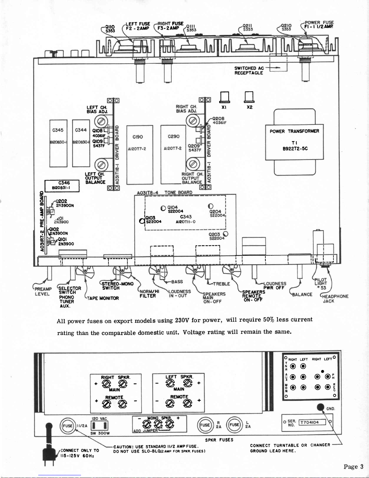
SWITCHED
AC
RECEPTACLE
LEFT
CH.
BIAS
ADJ.
I
xl
tr
x2
QIOS
L
40E6rF
o|osI
s437F
LEFT CH.
rrc-rEHIiHE
I
arzoert-t
I
ClG
6
ao
202
2tr3900N
G
=
I
lrJ
G,
o.
ryll€"3i"'*
F
E
r'
o
4
Qtol
2N3900
POWER
TRANSFORMER
TI
8922T2-5C
i
-
s22oo4
{31o.1"r.
o,fi
-----'l
r------'t
lll
mll.!
11
r
r
r ! !i[--l---.j
QilO
s353
LEFT
FI.|SE
F2
-2AnP
F3.zAMP
FUSE
STEREO.MONO
swrTcH
tHl
FILTER
cAUTTON
!
USE
STANDARo
lll2
AMP FUSE.
DO
NOT USE
StO-BLq(2AMP
FOR
SPKR.
FUSES)
Ft
-
| l/zalP
SELECTOR
swtTcH
PHONO
TUNER
AUX.
APE MONITOR
PWR OFF
SPEAI(ERS
ttnlloJti
All
power
fuses
on
export
models
using
230V
for
power,
will
requite
50Vo
less current
rating than the comparable
domestic
unit. Voltage
rating
will
remain
the
same.
COIITIIECT TURNTABLE
OR
CHANGER
GROUNO
LEAD
HERE.
ONNECT
OI{LY
TO
-dbru.
oR,crr
uErr
Rtc"r uErro
{o
o
to
Qo
o
o
or
Ho
o
o
oE
OO
RIGHT SPKR.
+@@
MAIN
REK)TE
+
+
LEFT
SPKR
@-^,P
REI'OTE
@@
ll5-125V
6OHr
SPKR
FUSES
Page 3
STRYICING
YOTTAGT
CHECKS
Preliminary checks of
the
D.
C. voltages
present
at
various
points
in
the
S-9500b
can
prove
useful
in 1o-
cating defective
components.
They
are
inconclusive,
however, in
determining
if transistors
are operating
properly
in
all aspects.
They
can
only indicate
wheth
-er
the transistor is open,
shorted
or functioning,
4!
how well
the transistor
is
functioning.
IN GENERAL:
Correct
voltages
indicate a functioning transistor.
The
same voltage
at
the collector
and
emitter
indicates a shorted
transistor.
Full supply
voltageon
the
collector
and
novoltage
on
the
emitter
indieates
an open transistor.
OUTPUT
TRANSISIOR
BIAS
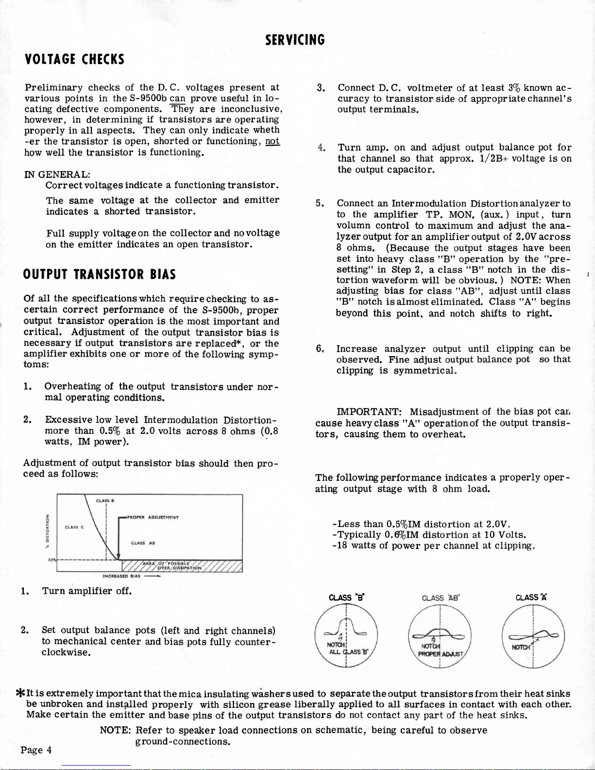
Of alt
the
specifications
which
require
checking to
as-
certain correet
performance
of the
S-9500b,
proper
output
transistor
operation is the
most
important
and
critical.
Adjustment
of
the
output
transistor
bias
is
necessary
if
output
transistors
are
replaced*,
or
the
amplifier exhibits
one or
more
of
the
following symp-
toms:
1. Overheating
of the output transistors
under
nor-
mal
operating conditions.
2.
Excessive
low level Intermodulation
Distortion-
more
than 0,5Vo
at
2.0
volts
across 8
ohms
(0.8
watts, IM
power).
Adjustment
of output
transistor
bias
should then
pro-
ceed as follows:
Connect
D. C.
voltmeter of at
least 370
known
ac-
curacy
to transistor
side of appropriatechannel's
output terminals.
Turn arnp. on
and
adjust
output
balance
pot
for
that channel
so
that
approx.
L/28+ voltage is
on
the
output capacitor"
Connect
an
Intermodulation
Distortion
analyzer
to
to the
amplifier TP.
MON.
(aux.
)
input , turn
volumn
control
to
ma:<imum
and adjust
the
ana-
lyzer
output
for
an amplifier output
of.
2.0V
across
I
ohms.
(Because
the
output
stages have been
set into
heavy
class
"8"
operation
by
the
"pre-
setting"
in Step 2,
a elass
"8"
notch in the
dis-
tortion
waveform
will be obvious.
)
NOTE:
When
adjusting
bias
for class
"A8",
adjust
until class
"8"
notch
is
almost eliminated.
Class
"A"
begins
beyond
this
point,
and
notch
shifts
to right.
Inerease
analyzer
output
until
clipping
can be
observed.
Fine adjust
output
balance
pot
so
that
clipping is
symmetrical"
3.
a.
6.
IMPORTANT: Misadjustment
of
the
bias
pot
car.
cause heavyclass
"A"
operationof
the output
transis-
tors,
causing
them
to overheat.
The
followingperformance
indicates
a
properly
oper-
ating
output
stage
with
8
ohm
load.
-Less
than
0.57oIM
distortion at
2.0V"
-Typically
0.
goIM
distortion at
t0
Volts.
-18
watts
of
power
per
channel
at clipping"
1"
Turn amplifier
off.
2. Set
output
balance
pots
(left
and right channels)
to mechanical
center
and bias
pots
fully counter-
clockwise.
{<
ft is extremely
important
that the
miea
insulating wishers
used to separate
the
output transistors fro
be
unbroken
and instilled
properly
with silicon
grease
liberally
applied
to
all surfaces
in contar
Make certain
the
emitter
and
base
pins
of
the
output
transistors do
not
contact
any
part
of
the he
NOTE:
Refer
to
speaker load
connections
on schematic,
being
careful to
observe
ground-connections.
Page
4
cL-Ass
"B'
CLASS H
 Loading...