

Page 1
XL-DH20NH
M
U
T
E
C
L
OC
K
/T
I
M
ER
AU
X
P
T
Y
R
D
S
SERVICE MANUAL
No. S7929XLH20NHH
MICRO COMPONENT SYSTEM
D
C
SB
U
E
T
U
M
MER
I
T
K/
C
LO
C
/
G
N
I
N
U
T
R
DE
L
O
F
Y
T
P
S
RD
X
AU
iPod is a trademark of Apple Inc., registered in the
U.S. and other countries.
CONTENTS
PRECAUTIONS FOR USING LEAD-FREE SOLDER
CHAPTER 1. GENERAL DESCRIPTION
[1] Safety Precaution For Service Manual ........1-1
[2] Specifications...............................................1-1
[3] Names Of Parts ........................................... 1-2
CHAPTER 2. MECHANISM BLOCKS
[1] Caution On Disassembly .............................2-1
CHAPTER 3. DIAGRAMS
[1] Block Diagram .............................................3-1
CHAPTER 4. CIRCUIT DESCRIPTION
[1] Waveforms Of Servo Circuit ........................4-1
[2] Voltage.........................................................4-2
MODEL
XL-DH20NH
XL-DH20NH Micro Component System consisting of
XL-DH20NH (main unit) and CP-DH20NH (speaker system).
• In the interests of user-safety (Required by safety regulations in some countries) the set should be restored to its
original condition and only parts identical to those specified
be used.
CHAPTER 5. CIRCUIT SCHEMATICS AND PARTS
LAYOUT
[1] Notes On Schematic Diagram ......................5-1
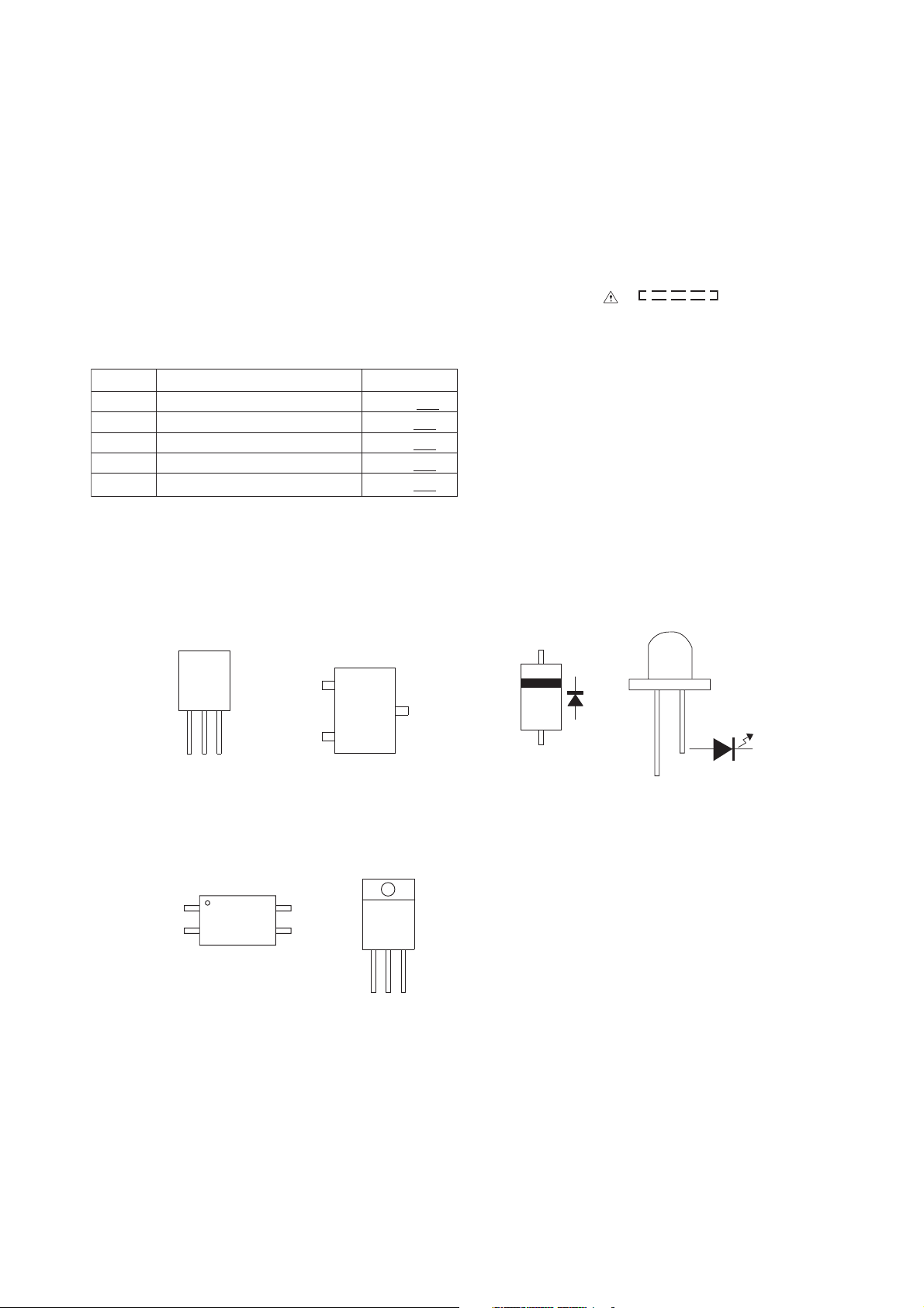
[2] Types Of Transistor And LED .......................5-1
[3] Schematic Diagram ......................................5-2
[4] Charts Of Connecting Wires .......................5-22
[5] Wiring Side Of PWB ...................................5-24
CHAPTER 6. FLOWCHART
[1] Troubleshooting ............................................6-1
CHAPTER 7. OTHERS
[1] Function Table Of IC .....................................7-1
[2] VFD Display..................................................7-2
PARTS GUIDE
Parts marked with " " are important for maintaining the safety of the set. Be sure to replace these parts with
!
specified ones for maintaining the safety and performance of the set.
SHARP CORPORATION
This document has been published to be used for
after sales service only.
The contents are subject to change without notice.
Page 2
XL-DH20NH
a
a
d
g
PRECAUTIONS FOR USING LEAD-FREE SOLDER
1. Employing lead-free solder
"MAIN, POWER, DISPLAY, HEADPHONE, USB, iPod, REFRESH PWB" of this model employs lead-free solder.
The LF symbol indicates lead-free solder, and is attached on the PWB and service manuals. The alphabetic
character following LF shows the type of lead-free solder.
Examples:
Indicates lead-free solder of tin, silver and copper.
2. Using lead-free wire solder
When fixing the PWB soldered with the lead-free solder, apply lead-free wire solder. Repairing with convention
lead wire solder may cause damage or accident due to cracks.
As the melting point of lead-free solder (Sn-Ag-Cu) is higher than the lead wire solder by 40 C, we recommen
you to use a dedicated soldering bit, if you are not familiar with how to obtain lead-free wire solder or solderin
bit, contact our service station or service branch in your area.
3.
Soldering
As the melting point of lead-free solder (Sn-Ag-Cu) is about 220°C which is higher than the conventional lead
solder by 40°C,and as it has poor solder wettability, you may be apt to keep the soldering bit in contact with the
PWB for extended period of time. However, since the land may be peeled of for the maximum heat-resistance
temperature of parts may be exceeded, remove the bit from the PWB as soon as you confirm the steady
soldering condition.
Lead-free solder contains more tin, and the end of the soldering bit may be easily corrected. Make sure to turn
on and off the power of the bit as required. If a different type of solder stays on the tip of the soldering bit, it is
alloyed with lead-free solder. Clean the bit after every use of it.
When the tip of the soldering bit is blackened during use, file it with steel wool or fine sand paper.
Be careful when replacing parts with polarity indication on the PWB silk.
Lead-free wire solder for servicing
Ref No.
PWB-A 92L701M5673006 MAIN
PWB-B 92L701CM904001 POWER
PWB-C 92L701CM903002 DISPLAY
PWB-D 92L701CM903005 HEADPHONE
PWB-E 92L701CM90300E USB
PWB-F 92L701CM90300W iPod
PWB-G 92L701CM90300Z REFRESH
Parts No.
Description
– 1
i
Page 3
XL-DH20NH
CHAPTER 1. GENERAL DESCRIPTION
[1] Safety Precaution For Service Manual
WARNINGS
THE AEL (ACCESSIBLE EMISSION LEVEL) OF LASER POWER OUTPUT FOR THIS MODEL IS SPECIFIED TO
BE LOWER THAN CLASS I REQUIREMENTS. HOWEVER, THE FOLLOWING PRECAUTIONS MUST BE OBSERVED
DURING SERVICING TO PROTECT YOUR EYES AGAINTS EXPOSURE TO THE LASER BEAM.
1- WHEN THE CABINET HAS BEEN REMOVED, THE POWER IS TURNED ON WITHOUT A COMPACT DISC,
AND THE PICKUP IS ON A POSITION OUTER THAN THE LEAD-IN POSITION, THE LASER WILL LIGHT FOR
SEVERAL SECONDS TO DETECT A DISC.
DO NOT LOOK INTO THE PICKUP LENS.
2- THE LASER POWER OUTPUT OF THE PICKUP INSIDE THE UNIT AND REPLACEMENT SERVICE PARTS
HAVE ALREADY BEEN ADJUSTED PRIOR TO SHIPPING.
3- NO ADJUSTMENT TO THE LASER POWER SHOULD BE ATTEMPTED WHEN REPLACING OR SERVICING
THE PICKUP.
4- UNDER NO CIRCUMSTANCES LOOK DIRECTLY INTO THE PICKUP LENS AT ANY TIME.
5- CAUTION - USE OF CONTROLS OR ADJUSTMENTS, OR PERFORMANCE OF PROCEDURES OTHER THAN
THOSE SPECIFIED HEREIN MAY RESULT IN HAZARDOUS RADIATION EXPOSURE.
This product is classified as a CLASS 1 LASER PRODUCT.
[2] Specifications
General
Power source AC 220 - 240 V ~ 50/60 Hz
Power
consumption
Dimensions Width: 155 mm (6-3/32")
Weight 2.12 kg (4.67 lbs.)
( * ) This power consumption value is obtained when the
main unit is in stand-by mode without iPod charging.
Power on: 45 W
Power stand-by: 0.6 W (*)
Height: 178 mm (7-1/64")
Depth: 243 mm (9-9/16")
Amplifier
Output power MPO: 50 W (25 W + 25 W) (10% T.H.D.)
Output
terminals
Input terminals AUX IN (Analogue input):
RMS: 50 W (25 W + 25 W) (10% T.H.D.)
Speakers: 6 ohms
Headphones: 16 - 50 ohms
(recommended: 32 ohms)
500 mV/47 k ohms
CD player
Type Single disc multi-play compact disc
Signal
readout
D/A converter Multi bit D/A converter
Frequency
response
Dynamic
range
player
Non-contact, 3-beam
semiconductor laser pickup
20 - 20,000 Hz
90 dB (1 kHz)
USB
USB host
interface
Support file MPEG 1 Layer 3
Bitrate support MP3 (32 ~ 320 kbps)
Other Maximum total number of MP3/
File system
support
Complies with USB 1.1 (Full
Speed)/ 2.0 Mass Storage Class.
Support Bulk only and CBI
protocol.
WMA (Non DRM)
WMA (64 ~ 160 kbps)
WMA files is 65280.
Maximum total number of folders
is 255 INCLUSIVE of root
directory.
The ID3TAG information
supported are TITLE, ARTIST and
ALBUM only.
Supports ID3TAG version 1 and
version 2.
Support USB devices with
Microsoft Windows/DOS/FAT 12/
FAT 16/ FAT 32.
2 kbyte block length for sector.
Tuner
Frequency range FM: 87.5 - 108 MHz
AM: 522 - 1,620 kHz
Speaker
Type
Maximum input
power
Rated input power 25 W
Impedance 6 ohms
Dimensions
Weight
2-way 2-speaker system
5 cm (2") tweeter
10 cm (4") woofer
50 W
Width: 132 mm (5-13/64")
Height: 260 mm (10-15/64")
Depth: 171.5 mm (6-49/64")
1.98 kg (4.36 lbs.)/each
1 – 2
1 – 1
Page 4
XL-DH20NH
4
3
2
1
[3] Names Of Parts
2
3
4
5
6
7
1
Front panel
1. iPod Docking Station
2. Remote Sensor
3. Timer Indicator
8
9
10
4. On/Stand-by Button
5. Function Button
6. Disc Tray
7. Headphone Socket
8. Volume Control
9. Disc / USB / iPod Play or Pause or
Stop Button
10. Disc Tray Open / Close Button
11. USB Terminal
11
19
20
12345678910
11
13 15
12
14 16
17
18
Display
1. MP3/WMA Folder Indicator
2. MP3/WMA Total Indicator
3. Memory Indicator
4. CD Indicator
5. MP3 Indicator
6. WMA Indicator
7. RDS Indicator
8. TA Indicator
9. PTYI Indicator
10. Extra Bass Indicator
11. TP Indicator
12. Sleep Indicator
13. Timer Play Indicator
14. Repeat Play Indicator
15. FM Stereo Mode Indicator
16. FM Stereo Receiving Indicator
17. Disc Play Indicator
18. Disc Pause Indicator
19. USB Indicator
20. Random Indicator
Speaker system
1. Tweeter
2. Woofer
3. Bass Reflex Duct
4. Speaker Wire
1 – 3
1 – 2
Page 5
XL-DH20NH
MUTE
CLOCK/TIMER
AUX
PTY
RDS
1
17
18
19
20
21
2
3
4
5
6
7
8
9
10
11
12
13
14
15
16
CD
USB
TUNING/
FOLDER
MUTE
AUX
22
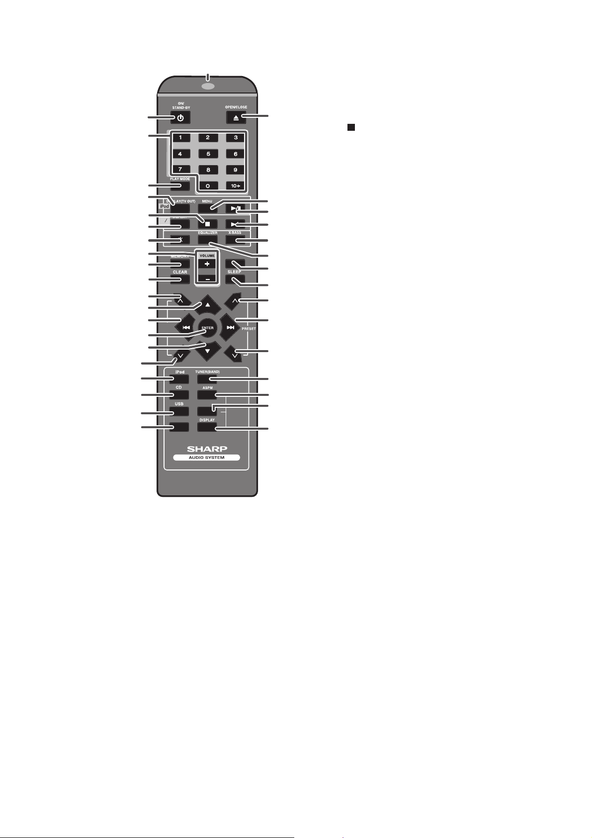
Remote control
1. Remote Control Transmitter
2. On / Stand-by Button
3. Direct Search Buttons
4. Play Mode Button
5. iPod Display (TV OUT) Button
6. CD / USB Stop Button
23
24
25
26
CLOCK/TIMER
27
28
29
30
31
32
33
PTY
RDS
34
35
36
7. CD / USB Display Button
8. Mute Button
9. Volume Up or Down Buttons
10. Memory Button
11. Clear Button
12. Folder Up / Tuning Up Button
13. iPod Cursor Up Button
14. Fast Reverse or Track Down Button
15. Enter Button
16. iPod Cursor Down Button
17. Folder Down / Tuning Down Button
18. iPod Button
19. CD Button
20. USB Button
21. AUX Button
22. Open / Close Button
23. iPod Menu Button
24. iPod Play / Pause Button
25. CD / USB Play / Pause Button
26. X-Bass Button
27. Equaliser Mode Button
28. Clock / Timer Button
29. Sleep Button
30. Preset Up Button
31. Fast Forward or Track Up Button
32. Preset Down Button
33. Tuner (Band) Button
34. RDS ASPM Button
35. RDS PTY Button
36. RDS Display Button
1 – 4
1 – 3
Page 6
XL-DH20NH
CD-ES700/CD-ES77CD-ES700/CD-ES77Service ManualCD-ES700/CD-ES77MarketE
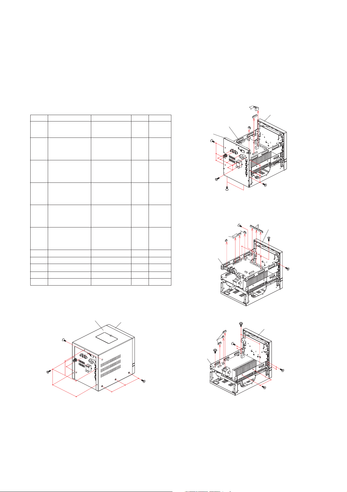
CHAPTER 2. MECHANISM BLOCKS
[1] Caution On Disassembly
Follow the below-mentioned notes when disassembling the unit and reassembling it, to keep it safe and ensure
excellent performance:
1. Take compact disc out of the unit.
2. Be sure to remove the power supply plug from the wall outlet before starting to disassemble the unit.
3. Take off nylon bands or wire holders where they need to be removed when disassembling the unit. After servicing
the unit, be sure to rearrange the leads where they were before disassembling.
STEP REMOVAL PROCEDURE FIGURE
1 Top Cover with 1. Screw .................. (A1)x6 1
iPod PWB 2. Screw .................. (A2)x5 1
3. Socket ................ (A3)x1 2
2 Rear Panel with PWB 1. Screw .................. (B1)x8 2
2. Screw .................. (B2)x6
3. Socket ................ (B3)x1
4. AC Cord .............. (B4)x1
3 Main PWB 1. Screw .................. (C1)x2 3
2. Screw .................. (C2)x2
3. Socket ................ (C3)x6
4. Flat Cable ........... (C4)x1
4 Power PWB 1. Screw .................. (D1)x3 4
2. Screw .................. (D2)x2
3. Screw .................. (D3)x4
4. Socket ................ (D4)x3
5 Front Panel Assy 1. Disc Tray Cover .. (E1)x1 5
2. Screw .................. (E2)x4 5
3. Hook ................... (E3)x2 5
4. Socket ................ (E4)X1 6
6 Display PWB 1. Knob ................... (F1)x1 6
2. Nut ...................... (F2)x1
3. Washer ............... (F3)x1
4. Screw .................. (F4)x8
7 Headphone PWB 1. Screw .................. (G1)x2 6
8 USB PWB 1. Screw .................. (H1)x2 6
9 Loader panel 1. Screw .................. (J1)x4 7
10 CD Mechanism Unit 1. Screw .................. (K1)x4 8
11 iPod PWB 1. Screw .................. (L1)x3 9
Rear Panel with PWB
(B1) x 3
M3 x 6mm
(B2) x 6
M3 x 8mm
Main PWB
Main PWB
M3 x 6mm
(C4) x 1
(C3) x 1
(B1) x 2
(A3) x 1
(C2) x 1
M3 x 6mm
(C3) x 2
(B4) x 1
(B3) x 1
Figure 2
Front Panel Assy
(B1) x 3
M3 x 6mm
(C3) x 3
Front Panel Assy
(C1) x 2
M3 x 6mm
(C2) x 1
M3 x 6mm
(A2) x 5
M3 x 8mm
(A1) x 3
M3 x 6mm
Figure 1
Figure 3
Front Panel AssyTop Cover
(D4) x 3
(D1) x 1
M3 x 6mm
Power PWB
(A1) x 3
M3 x 6mm
(D1) x 2
M3 x 6mm
(D3) x 2
M3 x 6mm
Front Panel Assy
(D3) x 2
M3 x 6mm
(D2) x 2
M3 x 8mm
Figure 4
2 – 1
Page 7
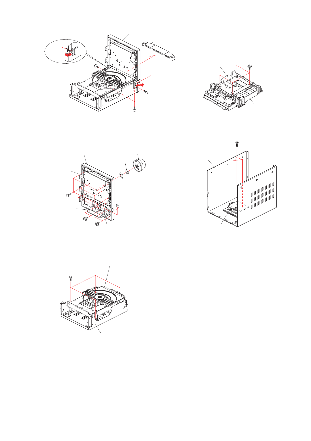
XL-DH20NH
Hook
(E3) x 1
PULL
Display PWB
(E2) x 1
M3 x 6mm
Front Panel Assy
Figure 5
Front Panel Assy
(F1) x 1
(F2) x 1
(F3) x 1
PULL
(E2) x 2
M3 x 6mm
Disc Tray Cover
(E1) x 1
Hook
(E3) x 1
(E2) x 1
M3 x 6mm
CD Mechanism Unit
Figure 8
Top Cover
(K1) x 4
Special Screw
(L1) x 3
M2.8 x 8mm
Loader Panel
(F4) x 8
M3 x 8mm
USB PWB
(H1) x 2
M3 x 8mm
(J1) x 4
M3 x 22mm
(G1) x 2
M3 x 8mm
Headphone PWB
Figure 6
Loader Panel
Main Chassis
Figure 7
(E4) x 1
iPod PWB
Figure 9
2 – 2
Page 8
XL-DH20NH
&
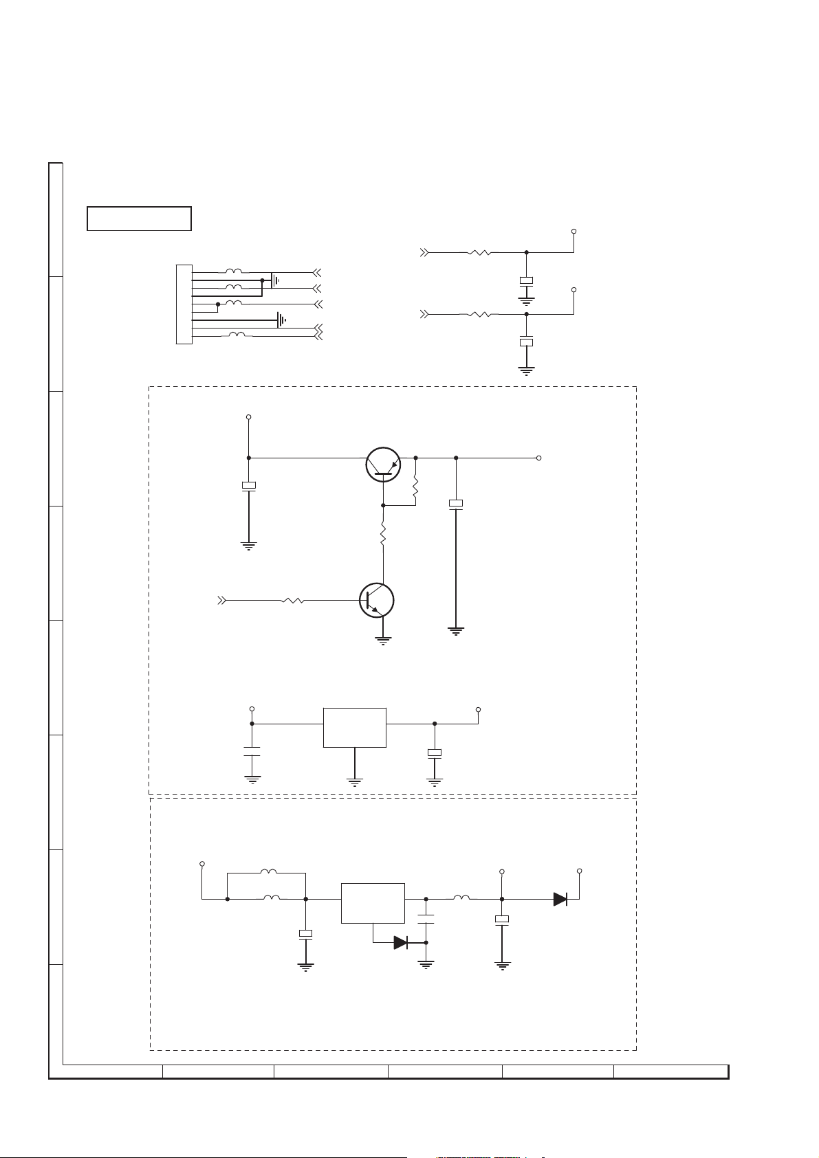
CHAPTER 3.
[1] Block Diagram
DIAGRAMS
TUNER JACK
TUNER ESD Protect
AM
L
SI4731
tuner vcc
Function:AM/FM/RDS
Function:CD & USB Decode
R
I2C
L
R
GND
NJM4558
AUDIO OUT
UPDATA
Function:VOL
MUTE
L
CD_AUDIO
R
MOTOR
DOOR MOTOR
HEADER
PICK UP
MOTOR
ABCDEF
FLASH
AN5888
MOTOR DRIVER
USB
KEY
DSA & IR
ALI M5673
DSA CONNECTOR
RESET
VCC CTRL
VFD DRIVER
PT6311
Figure 3-1: BLOCK DIAGRAM (1/2)
3 – 1
Page 9
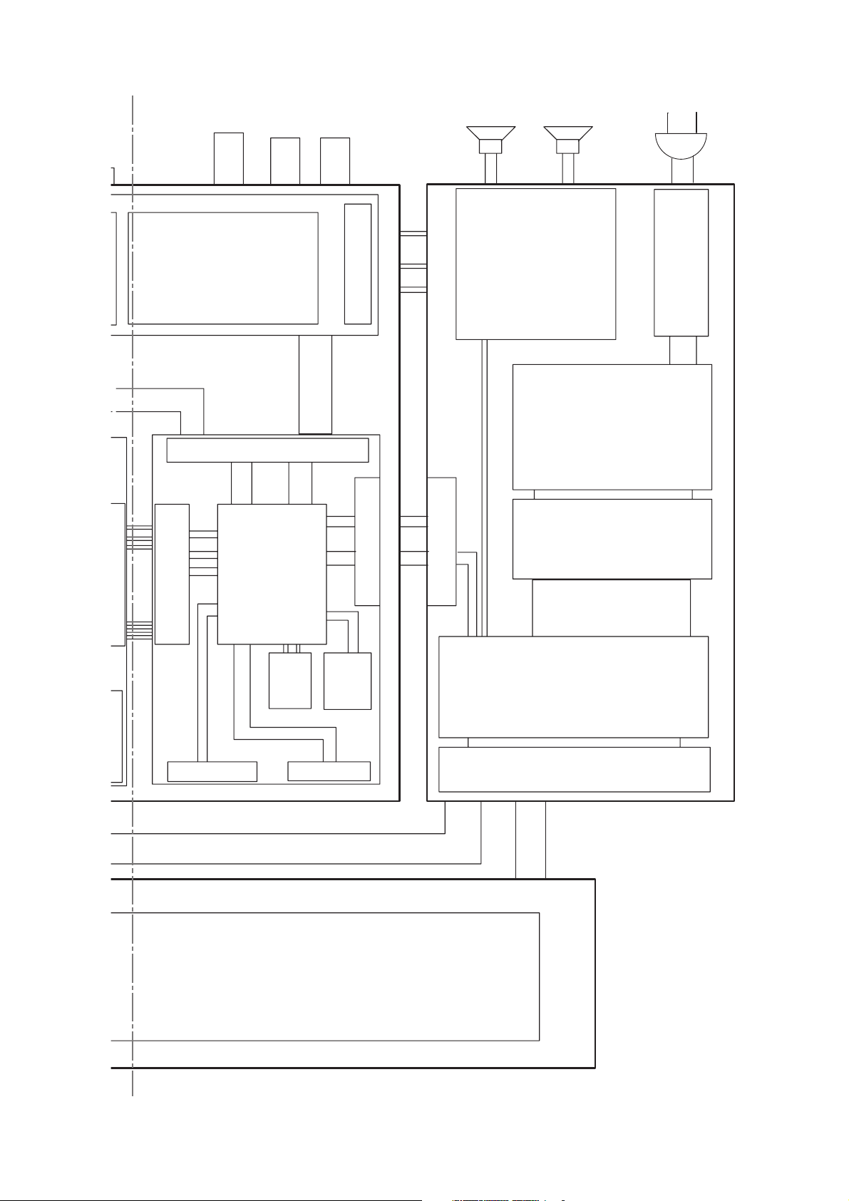
XL-DH20NH
DSA
CONNECTOR
VIDEO
AUXL
n:VOL&EQ&CHANNELS CTRL
NJU7391
I2C&STB CONNECTOR
MCU
RS21266
DSA CONNECTOR
AUXR
AUDIO OUTPUT
I2C & STB
VCC CTRL
L
R
GND
Amplifier
TDA7265(25W+25W)
Filter and commute
PWM + MOS
7M0880+FSDM311
VCC CONNECTION
TRANSFORMER
(EI33+EL19)
VCC CTRL
Commutate
EEPROM
IPOD JAC
VFD JACK
All VCC CONNECTION
VFD DISPLAY
RESET
VCC OUTPUT Filter & CRTL
VCC CONNECTOR
VFD CON
Figure 3-2: BLOCK DIAGRAM (2/2)
3 – 2
Page 10
XL-DH20NH
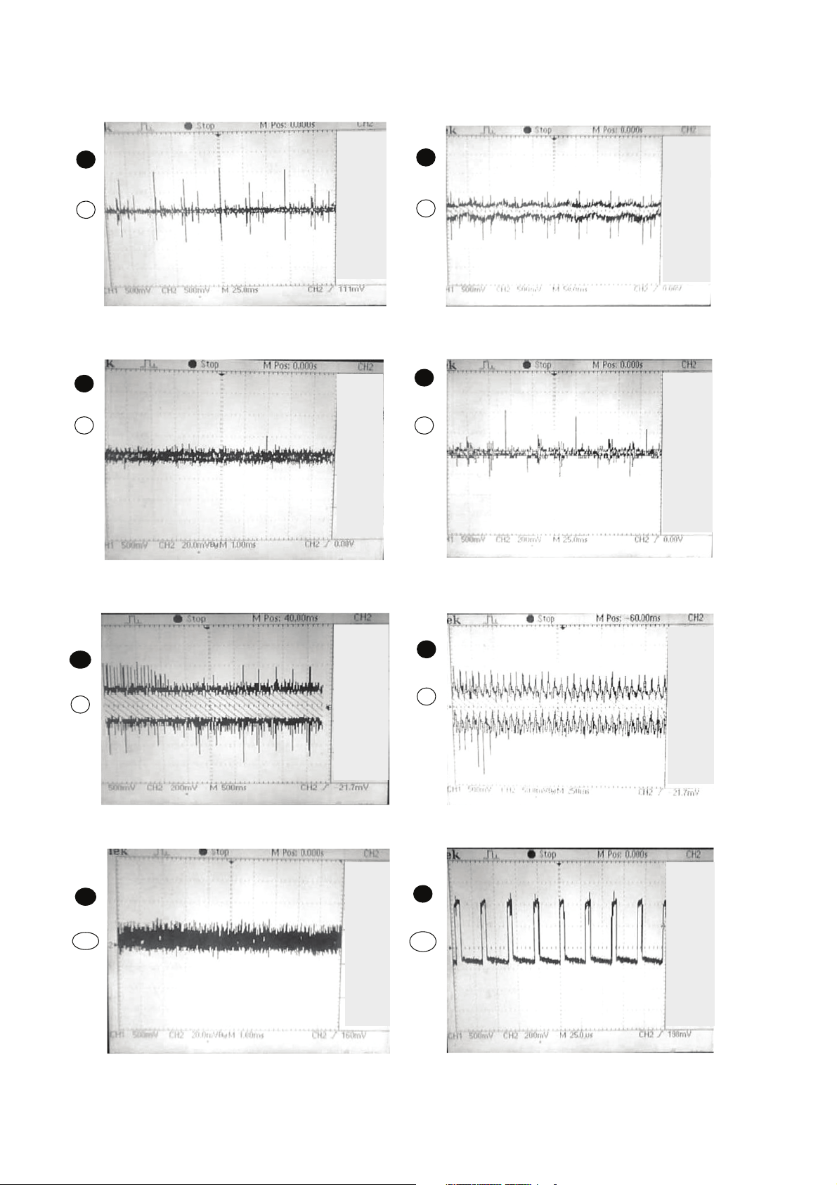
CHAPTER 4. CIRCUIT DESCRIPTION
[1] Waveforms Of Servo Circuit
U5
U5
U5
2
TCO
2
Figure 2
4
1
FCO
1
Figure 1
3
U5
PD
3
FE
16
U5
17
5
U5
124
Figure 3 Figure 4
TE
6
SB
U5
18
Figure 5 Figure 6
SPDCO
7
SCO
8
U5
126
Figure 7
Figure 8
4 – 1
Page 11
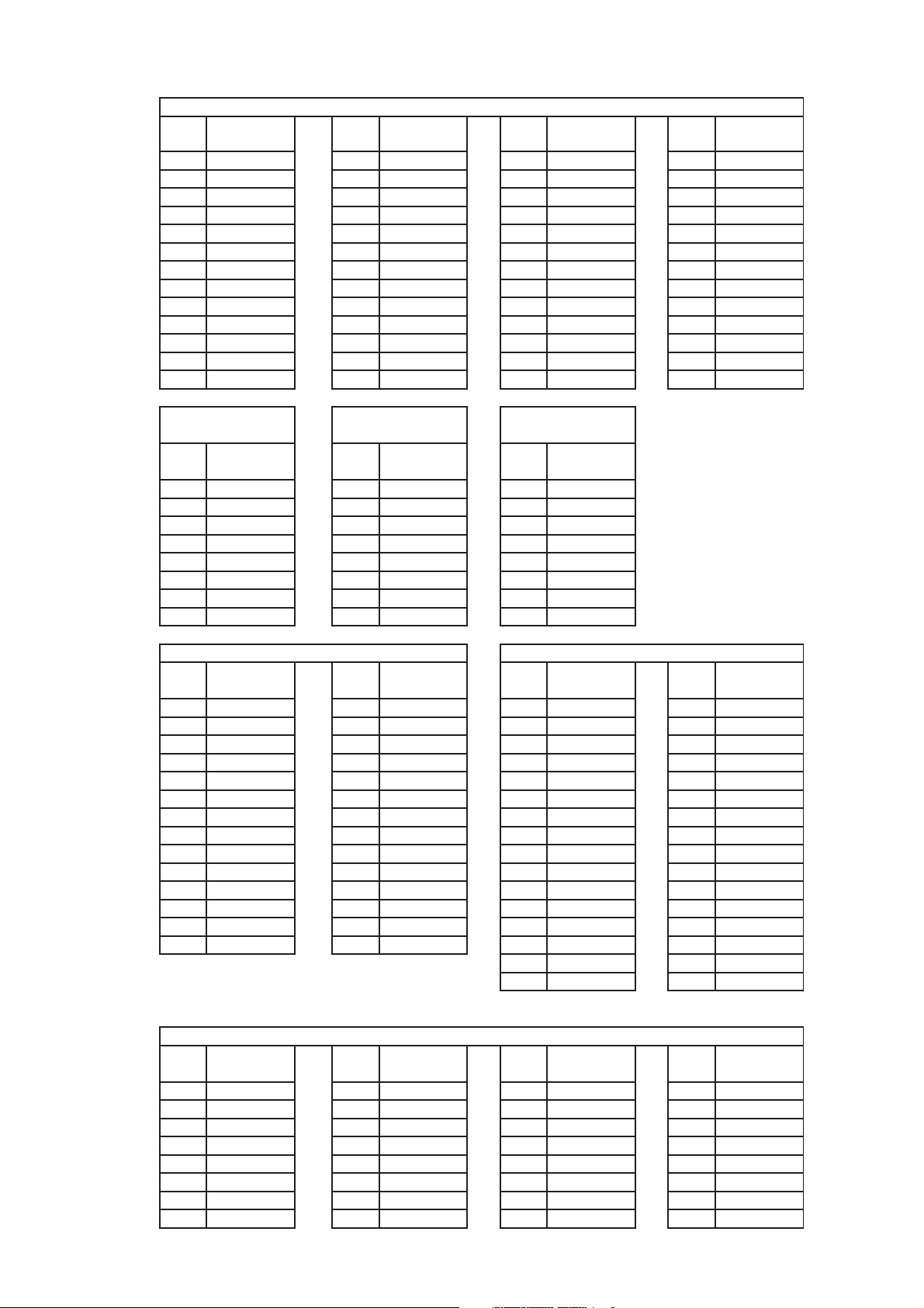
[2] Voltage
U1 (P16311 / DISPLAY PWB)
PINNOVOLTAGE
(V)
1 0.000 14 5.190 27 -13.26 40 -19.28
2 5.190 15 -15.42 28 -13.30 41 -19.10
3 5.190 16 -11.72 29 -19.66 42 -19.15
4 0.000 17 -23.60 30 -18.72 43 -19.30
5 0.930 18 -23.60 31 -19.20 44 -19.68
6 0.930 19 -23.60 32 -19.55 45 5.190
7 0.150 20 -15.67 33 5.190 46 5.160
8 0.140 21 -15.37 34 -24.00 47 5.190
9 1.250 22 -15.66 35 -19.36 48 5.190
10 2.500 23 -13.62 36 -19.02 49 5.190
11 2.500 24 -23.60 37 -18.96 50 5.180
12 2.520 25 -21.60 38 -19.93 51
13 0.030 26 -23.60 39 -18.94 52
PINNOVOLTAGE
(V)
PIN
NO
VOLTAGE
(V)
PINNOVOLTAGE
(V)
0.000
2.860
XL-DH20NH
U2 (EON F20)U1 (D4558)
PINNOVOLTAGE
1
2
3
4 -12.45 4 0.000 4
5
6
7
8
PINNOVOLTAGE
1
2
3
4
5
6
7
8
9
10
11
12
13
14
(V)
0.000
0.000
0.000
0.000
0.000
0.000
12.150
U3 (AN5888)
(V)
1.570
0.020
3.050
1.580
1.220
0.000
0.000
5.200
0.020
0.020
2.760
2.550
2.720
2.600
PINNOVOLTAGE
1
2
3
5
6
7
8
PINNOVOLTAGE
15
16
17
18
19
20
21
22
23
24
25
26
27
28
(V)
0.090
1.350
3.270
0.220
1.290
3.270
3.270
(V)
2.550
2.790
3.340
1.970
5.190
0.000
1.450
0.000
1.820
0.000
5.170
1.580
1.570
2.290
U7 (24C02)
PINNOVOLTAGE
1
2
3
5
6
7
8
PIN
NO
1
2
3
4
5
6
7
8
9
10
11
12
13
14
15
16
(V)
0.000
0.000
0.000
0.000
3.690
3.560
0.000
3.960
U8 (NJU7391)
VOLTAGE
(V)
3.790
3.750
3.790
3.790
3.790
3.810
3.800
1.800
3.810
3.790
3.700
3.640
0.040
3.960
3.620
1.250
PINNOVOLTAGE
17
18
19
20
21
22
23
24
25
26
27
28
29
30
31
32
(V)
2.620
0.610
0.000
3.960
3.710
1.680
3.960
3.960
3.690
3.690
0.000
0.000
0.000
0.000
0.660
3.700
PINNOVOLTAGE
1
2
3
4
5
6
7
8
(V)
0.040
3.960
2.700
1.190
0.000
1.610
3.710
3.940
U6 (RF21266)
PINNOVOLTAGE
9
10
11
12
13
14
15
16
(V)
4.260
0.000
3.810
3.810
0.000
0.000
3.690
3.630
4 – 2
PINNOVOLTAGE
17
18
19
20
21
22
23
24
(V)
1.240
8.600
8.590
3.780
3.810
3.810
3.800
3.810
PIN
NO
25
26
27
28
29
30
31
32
VOLTAGE
(V)
3.810
3.800
3.820
3.790
3.790
3.790
3.800
3.800
Page 12
XL-DH20NH
PINNOVOLTAGE
1
2
3
4
5
6
7
8
9
10
11
12
13
14
15
16
17
18
19
20
21
22
23
24
25
26
27
28
29
30
31
32
(V)
2.010
1.670
1.650
1.710
1.730
1.790
1.740
3.300
1.580
1.190
0.000
1.200
1.190
1.200
1.720
1.340
1.750
3.300
1.650
2.290
0.000
0.000
3.290
1.770
3.300
1.290
0.870
0.000
1.750
0.000
1.510
1.510
U5 (M5673)
PINNOVOLTAGE
33
34
35
36
37
38
39
40
41
42
43
44
45
46
47
48
49
50
51
52
53
54
55
56
57
58
59
60
61
62
63
64
(V)
1.510
1.510
1.510
1.520
0.000
3.300
1.260
1.380
1.510
1.390
1.360
2.110
0.760
1.510
0.760
1.700
2.450
1.390
0.000
0.000
1.750
0.000
0.000
3.300
0.220
1.440
0.100
0.850
3.300
3.300
1.150
1.150
PIN
NO
65
66
67
68
69
70
71
72
73
74
75
76
77
78
79
80
81
82
83
84
85
86
87
88
89
90
91
92
93
94
95
96
VOLTAGE
(V)
1.420
1.620
1.660
1.410
1.510
0.000
1.650
3.720
3.720
3.960
1.440
1.450
1.370
1.350
1.380
1.010
0.000
1.750
1.780
0.000
3.300
3.300
0.770
0.800
3.300
3.300
0.000
0.770
0.740
3.300
0.000
0.750
PINNOVOLTAGE
97
98
99
100
101
102
103
104
105
106
107
108
109
110
111
112
113
114
115
116
117
118
119
120
121
122
123
124
125
126
127
128
(V)
0.730
0.730
3.300
0.710
0.720
0.720
0.690
0.580
3.300
0.000
0.560
0.530
0.570
0.000
3.300
0.000
3.300
0.000
1.750
3.300
1.350
1.350
1.390
1.570
1.610
3.300
1.870
0.000
1.580
1.540
1.630
0.220
PINNOVOLTAGE
1
2
3
4
5
6
7
8
9
10
(V)
0.000
0.000
0.000
0.000
0.000
3.230
3.640
3.690
1.150
0.200
U4 (SI4731)
PIN
NO
11
12
13
14
15
16
17
18
19
20
VOLTAGE
(V)
0.340
0.260
0.360
0.770
0.000
0.470
0.720
0.000
3.230
0.000
U3
PIN VOLTAGE PIN VOLTAGE
NO
1
2
3
4
5
6
7
8
9
10
11
12
13
14
15
16
17
18
19
20
21
22
23
24
25
26
27
28
(V)
1.570
0.020
3.050
1.580
1.220
0.000
0.000
5.200
0.020
0.020
2.760
2.550
2.720
2.600
2.550
2.790
3.340
1.970
5.190
0.000
1.450
0.000
1.820
0.000
5.170
1.580
1.570
2.290
(MF1341S2161)(AN5888)
NO
1
2
3
4
5
6
7
8
9
10
11
12
13
14
15
16
17
18
19
20
U12
(V)
1.570
0.020
3.050
1.580
1.220
0.000
0.000
5.200
0.020
0.020
2.760
2.550
2.720
2.600
2.550
2.790
3.340
1.970
5.190
0.000
4 – 3
Page 13
XL-DH20NH
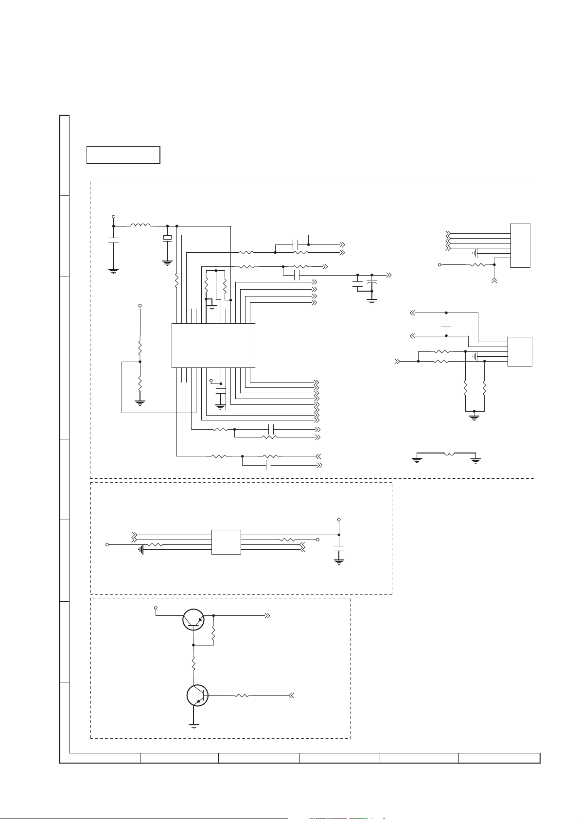
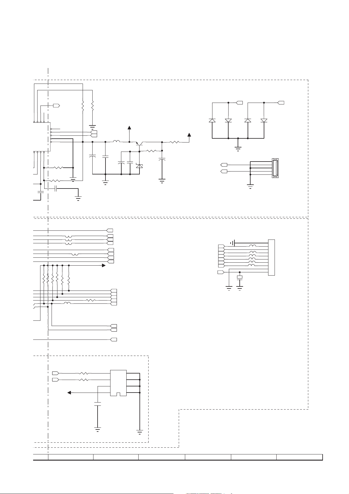
CHAPTER 5. CIRCUIT SCHEMATICS AND PARTS LAYOUT
[1] Notes On Schematic Diagram
•Resistor:
To differentiate the units of resistors, such symbol as K and M are
used: the symbol K means 1000 ohm and the symbol M means
1000 kohm and the resistor without any symbol is ohm-type resistor. Besides, the one with “Fusible” is a fuse type.
• Capacitor:
To indicate the unit of capacitor, a symbol P is used: this symbol P
means pico-farad and the unit of the capacitor without such a symbol is microfarad. As to electrolytic capacitor, the expression
"capacitance/withstand voltage is used".
(CH), (TH), (RH), (UJ): Temperature compensation
(ML): Mylar type
(P.P.): Polypropylene
REF. NO
VOL1 VOLUME MAX -- MIN
K1 ON/STAND-BY ON -- OFF
K2 FUNCTION ON -- OFF
K3 PLAY/PAUSE ON -- OFF
K4 OPEN/CLOSE ON -- OFF
type
DESCRIPTION POSITION
• Schematic diagram and Wiring Side of P.W.Board for this model are
subject to change for improvement without prior notice.
• The indicated voltage in each section is the one measured by Digital Multimeter between such a section and the chassis with no signal given.
1. In the tuner section,
indicates A M
indicates FM stereo
2. In the CD section, the CD is stopped.
• Parts marked with “ ( ) are important for maintaining the safety of the set. Be sure to replace these parts with
specified ones for maintaining the safety and performance of the
set.
“
[2] Types Of Transistor And LED
FRONT
VIEW
ECB
(S)(G)(D)
(1)(2)(3)
S8550
L431
TOP
VIEW
EL817
(3)
(1)
B
E
TOP
VIEW
HY3D
HY4D
HA7
H1A
H2A
1Y
09S
FRONT
VIEW
BCE
SB772
(2)
TOP VIEW
C
FRONT
VIEW
1N4007
SB360
1N5399
1N4148
92L11103R02002
92L11103R06001
5 – 1
Page 14
XL-DH20NH
[3] Schematic Diagram
A
B
MAIN PWB-A
CON 2.0mm(1x9)/AMP/PWR
CON13
1
2
3
4
5
6
7
8
9
1
2
3
4
5
6
7
8
9
1000RH
1000RH
7R/2A
300RH
FB2
FB40
FB44
VCC
FB3
GND
GND
A-12V
A+12V
VCC
POWER_OFF
AMP-MUTE
A+12V
A-12V
R079 2R2
R078 2R2
E5/1
100UF/16V
E8/1
100UF/16V
C
EC35
470UF/10V
GND
Q8
2SB772
R052
R053
10K
1K
EC27
470UF/10V
+12V
-12V
GND
GND
AUDIO/VCC
D
3904
CD_POWER_CTRL
R054
10K
Q7
GND
GND
E
3
VIN
IC2
AM1117-1.8V
ADJ
1
GND
VOUT
3V3
2
EC14
220UF/10V
GND
MAIN VCC
AUDIO/VCC
C022
104P
GND
F
VCCC
G
NC
1000RH
FB45
FB19
EC30
47UF/10V
GND
3
VIN
IC1
AM1117-1.8V
ADJ
1
D16
IN4148
VOUT
FB1
2
C038
104P
GND
1000RH
MCU3V9
100UF/10V
GND
MCU_VCC/VREF
D8
IN4148
EC43
H
MCU VCC
1
23456
Figure 5-1: MAIN (VCC AND MCU VCC) SCHEMATIC DIAGRAM
5 – 2
Page 15
XL-DH20NH
A
B
C
D
MAIN PWB-A
104P
MVCC
C62
GND
3V3-A
R130
20K
R30
12K
MOTOR-GND
L561000RH
100UF/10V
MOTOR-GND
Motor
EC26
R62
39K
23
25
27
BIAS28MUTE
VINLD24OPOUT
TRB_226VINTK
VINFC2TRB_13REGO24VINSL+5REGO16FWD7REV8VCC19VOTR-10VOTR+11VOSL+12VOSL-13VOFC-14VOFC+
1
SLEGP
FOCUS
R42
82K
MOTORGND
22
GND
CD5V
C69
0.1uF/0603
MOTOR-GND
R29
21K
R34
39K
CON2
1
SPIN+
2
SPIN-
3
SLED+
4
SLED-
5
LIMIT1
6
LIMIT2
CON 2.0mm(1x6)
LIMIT
CON5
1
LOAD+
2
LOAD-
3
IN
4
GND
5
OUT
3V3-A
SPIN+
SPIN-
SL+
SL-
MOTOR-GND
R64
R63
R43
10K/0603
C023
0.1U
2.2K/0603
1K/0603
MOTOR-GND
C021
15
VOTK+
VOTK-
TRACK
SPINDLE
U3
AM5888
0.01UF
R39
R41 1K
C001
0R
0.47UF
R35
39K
R38
3K9
56K
R49
16
17
18
19
VCC220OPIN21VCTL
VOLD+
VOLD-
SPIN-
SPIN+
TRACK-
TRACK+
XSPINDLE
C017
104P
VREF_16
XTRACK
EC6
10uF
MOTOR-GND
OPEN/CLOSE
VREF_16
120-pin
LOAD+
LOAD-
CON5-2.0
FOCUS+
TRAY_OUT
TRAY_IN
0.047UF
C019
R33 0
R40
C020
0.01U
FOCUS-
SLSL+
LOAD+
LOADTRAY_OUT
TRAY_IN
VREF_16
XSLEGP
0
XFOCUS
VREF_16
GND
FB11
1000RH
R65
47K/0603
R58
22K/0603
MOTOR-GND
MOTOR-GND
E
Flash
3V3-A
U9
3V3-A
F_CS
F_DI
GND
R95 100K
WP
GND
1
CS#
2
DO
3
WP#
4
GND5DI
F
VCC
Q16
2SB772
G
Q17
3904
H
1
23456
R09
10K
R06210K
GND
Figure 5-2: MAIN (MOTOR, FLASH AND USB VCC) SCHEMATIC DIAGRAM
HOLD#
SFLASH/2M
VCC
CLK
8
7
6
R029
1K
HOLD#
R9 100K
MVCC
USB VCC
5 – 3
F_CLK
F_DO
USB-VCC_CTRL
3V3-A
GND
C48
0.1UF
Page 16
XL-DH20NH
P
R061
10K/NC
2
0
3
O
F
D
MAIN PWB-A
L44
300RH
L45
300RH
TUNER_3V3
R69
10K
R9
R18
10K
47K
R16 22R
R17 22R
FMI
T1
4
3
AMI
C38
470P
R71
4
5
5
2
6
6
1
AMT
GND
0R
T-RCLK
T-SDIO
L41
U4
100UH/NC
3
2
1
C78
30P
C79
0.47uF
SI4731
GND
1
2
3
GND
4
5
X2
32.768KHZ
XIN
C82
22P
NC
NC
FMI
FRGND
AMI
RST
SEN7SCLK8SDIO9RCLK10VIO
6
GND
16NC17P318P219P120
15
NC
14
LOUT
13
ROUT
12
GND
11
VDD
R
1
R
1
C87
22P
C83
A
TUNER
Function:AM/FM/RDS
B
TUN-RST
TUN-CLK
I2C/SDA
C
R15 22R
MCU
CPU3V9
D
E
iPod-SDA
iPod_RXD
CD_POWER_CTRL
TRAY_IN
TRAY_OUT
LED
iPod_RST
iPod_TXD
OPEN/CLOSE
R021
R020 10K
R019
R018
R066
FB17 FB
F
R88 10K/NC
G
H
10K
10K
10K
10K
FB10 33R
FB8 33R
10K
R026 10K
R027 10K
R023
CPU3V9
POWER_OFF
Q20
3904
GND
R0210K
R01110K
R012NC
U6
23
24
R092100K
P0-7
P0-6
P0-5
P0-4
P0-3
P0-2
P0-1
P0-0
R060R
X1 32.678KHZ
1
C3
22P
GND
3-3
P3-4
R5F21266S QFP
$PIN02P3-73RESET4P4-75VSS6P4-67VCC8MODE
C6
R022100R
D7 IN4148
25
26
27
28
29
30
31
32
22P
Q6
R082
100
8550
GND
R06410K
10UF/10V
EC63
GND
GND
R07
0R
C4
22P
CPU3V9
17
P1-418P1-319P1-220P4-221P1-122P1-0
P1-5
P1-6
P5-3
P5-4
P3-1
P3-6
P1-7
P4-5
TP81
D61N4148
GND
16
15
14
13
12
11
10
9
2200UF/10V
104P
C2
FB15
R089
47K
FB50
0R
0R
U20
RCR5102
GND
MCU/VREF
I2C/SDA
I2C/CLK
AU
EE
TEST
1
23456
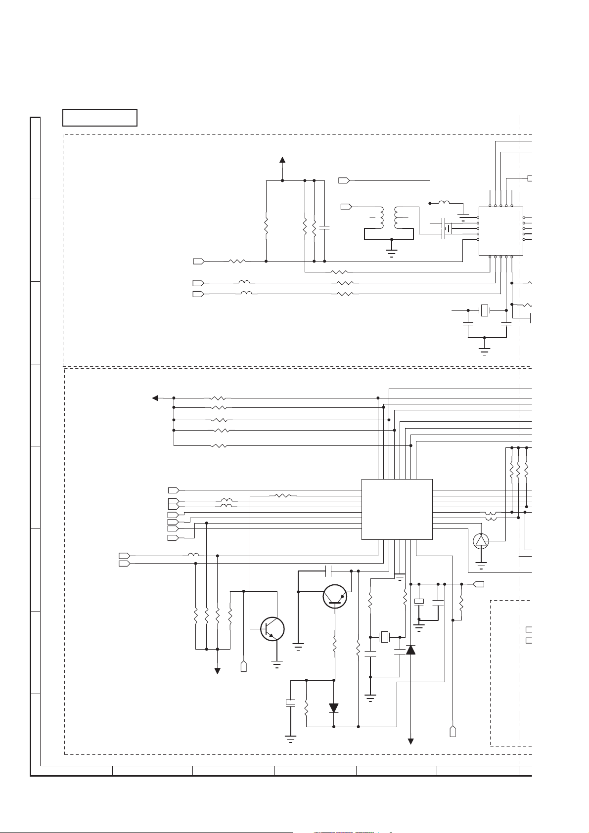
Figure 5-3: MAIN (TUNER AND MCU) SCHEMATIC DIAGRAM (1/2)
5 – 4
Page 17
XL-DH20NH
7
19
R11
R13
XIN
16NC17P318
P1
P2
15
NC
14
LOUT
13
ROUT
D
ND
GND
VDD
SCLK8SDIO9RCLK10VIO
22P
C83
12
11
R2
10K(NC)
R3
1OR
C87
104PF
GND
10K
10K
GND TUNER_3V3
TUNER-L
TUNER-R
T3V3
+
EC3
104PF
100u/10V
GND
L9
C84
47u/10V
GND
D1
IN4148/NCD2IN4148/NCD3IN4148D4IN4148
Q1
100UH
8050
13
R1
330
2
+
C35
C27
103PF
Z1
3.9V
R50 2R2
+
EC32
100u/10V
GND
AUDIO/VCC
AMI
FMI
FMI
GND
GND
CON6
1
2
3
4
5
AM/FM/JACK
AMI
0R
0R
U20
RCR5102
D
U/VREF
R0210K
I2C/SDA
I2C/CLK
R01110K
R012NC
AUDIO/VCC
FB5
300RH
FB4
300RH
FB6
300RH
FB9
R061
R01410K
R01510K
10K/NC
FB28 22R
300RH
R01 22R
R05 22R
R04 22R
C5
104P
CPU3V9
SDA
5
SCL
6
TP
7
VCC
8
KEY
CD-SCK
CD-SDA
CD/DVD-STB
MCU/VREF
AMP-MUTE
VFD_SDA2
iPod_VCC_CTRL
VFD_STB1
iPod_DET
USB-VCC_CTRL
TUN-RST
VFD_CLK
I2C/CLK
I2C/SDA
IR
AT24C02
U7
GND
A2
A1
A0
CON11
GND
MVCC
LED
KEY
VFD_SDA2
VFD_CLK
VFD_STB1
IR
MVCC
4
3
2
1
GND
GND
FB38
FB26
FB24
FB21
FB23
FB22
EC36
220UF/10V
300RH
300RH
300RH
300RH
300RH
300RH
1
2
3
4
5
6
7
8
9
10
CON 2.0mm(1x9)/KB/VFD
EEPROM
7
GND
GND
8 9 10 11 12
Figure 5-4: MAIN (TUNER AND MCU) SCHEMATIC DIAGRAM (2/2)
5 – 5
Page 18
XL-DH20NH
A
MAIN PWB-A
B
C
iPod_VCC
VCC
GND
R10
EC21
R055 10K
104P
Q9
2SB772
C065
R056
EC38
220UF/10V
GND
560
Q15
2N3904
NC
D
iPod_VCC_CTRL
10K
VCC
iPod+3V3
8050
R0590R
Q11
R89 680R
10UF/10V
EC31
ZD2
3V9
GND
R058 0R
R03 0R
C58
EC37
104P
47UF/10V
GND
E
GND
iPod POWER
F
G
H
1
23456
Figure 5-5: MAIN (iPod POWER) SCHEMATIC DIAGRAM
5 – 6
Page 19

-MEMO-
XL-DH20NH
5 – 7
Page 20
XL-DH20NH
50
117
A
G
A
OPU
B
C
FELPFO
D
E
F
TELPFO
SBLPFO
CON1
SF-P200Z(FPC)
4
4
3
3
2
2
1
1
CON 2.0mm(1x4)/USB
CON9
VC
VCC
GND
LD
VR
MD
FE1
TE1
SB1
D10
1
2
3
E
4
D
5
A
6
B
7
C
8
F
9
10
11
12
13
F+
14
T-
15
T+
16
F-
FB7
FB51
1000RH
D9
R48 33K/0603
R37 33K/0603
LD
Q18
2SB1132/(SOT89)
HAVC
GND
C039 0.1uF/0603
GND
C032
C034 30pF/0603
GND
6V8
80R/100MHz
0R
R67
R68 0R
C36
100UF/10V
6V8
GND
10uF/10V
0.1uF/0603
C035
30pF/0603
GND
GND
AUDIO/VCC
EC16
R45
1M
TNI
MDPUH
MAPUH
MBPUH
MCPUH
TPI
MDI
FOCUS+
TRACKTRACK+
FOCUS-
R36
15R/0603
EC9
47uF/16V
GND
EC11
10uF/10V
DP
DM
HAVC
0.1uF/0603
C025
0.1uF/0603
0R/0603
R23
X3
16.9344MHz
0R/0603
R24
C024
FB59
80R/100MHz
2
C30`
10uF/10V
M33V_LDO
GND
LDO
0.1uF/0603
EC8
GND
GND
GND
0.1uF/0603
FB61
80R/100MHz
EC10
100uF/10V
1
SEV_3V3
C018 0.1uF/0603
C052
GND
RF_1V8
12
47uF/16V
EC28
GND
C030
0.1uF/
0603
GND
C033 0.1uF/0603
3V3-A
C028
0.1uF/0603
C040 0.1uF/0603
SEV_3V3
V18
EC4
100uF
LINE_L
LINE_R
AUD_3V3
LDO
TPI
TNI
MCPUH
MBPUH
MDPUH
MAPUH
FELPFO
TELPFO
SBLPFO
C031
GND
100UH
12
M33V_CKG
GND
GND
C042
C041
AUD_GND
EC15
1uF/
0603
L1
100uF/10V
Chip Decap.
82nF/0603
82nF/0603
104P
C037
VREF_16
XSLEGP
XSPINDLE
XFOCUS
XTRACK
U5
10
11
12
13
14
15
16
17
18
19
20
21
22
23
24
25
26
27
28
29
30
31
32
33
34
35
36
37
38
MDI
1
LDO
2
TP1
3
TP2
4
MC
5
MB
6
MD
7
MA
8
AVDD33_2
9
HAVC
V12
AVSS33_2
TELP
MPXOUT1
MPXOUT2
MPXOUT3
COSP
COSN
AVDD33_3
VTB
VTP
AVSS33_3
AVSS33_LDO
AVDD33_LDO
AVDD18_LDO
AVDD33_CKG
XTALI
XTALO
AVSS33_CKG
AVDD18_1
AVSS18_1
BCAPIL
BCAPOL
LINEOUTL
BCAPIR
BCAPOR
LINEOUTR
AVSS33_AUD
AVDD33_AUD
GND
100uf/10V
C051 0.1uF/0603
127
128
MDI
FMINR
39
40
SEV_3V3
EC12
122
123
124
125
126
FOO
TRO
DMO
GPWM
AVSS33_1
FMINL
MICIN46V15L
MICBIAS
LINEINR
LINEINL
42
41
44
45
43
120
121
FMO
VREF16
AVD33_1
V08R
V08L
47
118
119
BTN ADIN2
BTN_ADIN3
VREF
V15R
49
48
C043
EC17
AUD_GND
1uF
EC18
EC22
10uF
1uF
EC19
AUD_
1uF
1uF
EC20
RESET
3V3-A
R26
G
EC41
10uF
R27 22K
D5 IN4148
R28
H
1
23456
10K
Q2
2N3904
22K
2
RESETJ
C027
0.1uF
13
GND
BC4
0.1uF/0603
AUD_3V3
BC5
AUD_GND
0.1uF/0603
BC6
0.1uF/0603
C060
0.1uF
3V3
GND
EC25
100uF/10V
0.1uF/0603
Figure 5-6: MAIN (SERVO) SCHEMATIC DIAGRAM (1/2)
5 – 8
Page 21

XL-DH20NH
43
124
SEV_3V3
603
123
DMO
AVSS33_1
MICBIAS
LINEINL
44
EC17
3
3
120
121
122
FMO
AVD33_1
V15L
V08L
46
47
45
1uF
1uF
EC18
EC19
AUD_GND
EC22
10uF
AUD_GND
AVDD3V3
117
118
119
VREF16
BTN_ADIN1
BTN_ADIN2
BTN_ADIN3
ALi M5673
VREF
V15R
V08R
SFGP
49
48
50
1uF
1uF
EC20
C059 0.1uF/0603
V18_CORE
VDD_PAD
GND
111
114
115
116
112
113
GPIOJ2
VDD_PAD
GND_PAD
AVDD_D33
VDD_CORE
GND_CORE
SFGN
DP
VDD_CORE
GND_CORE
DM
GND_PAD
51
53
54
55
52
56
GND
DP
DM
V18_CORE
VDD_PAD
GND
100K/0603
10K/0603
106
107
108
109
110
GPIOI5
GPIOI6
GPIOJ1
GPIOI7/I2S_CLK
GPIOJ0/I2S_DAT
XGPIOC0/SFCSB
XGPIOB7/SFDI
VDD_PAD
XGPIOB6/SFDO
XGPIOC1/SFSCK
60
59
57
58
61
105
R25
R59
104
GND
LIMIT
103
GPIOI2/IRC
GPIOI3_PWM1
GPIOI4_PWM2
GPIOI1/PWM0
GPIOI0/LCDWRJ
GPIOH7/LCDRDJ
PRSTB
GPIOH6/LCDCSJ
GPIOH5/LCDA0
GPIOH4/DATA7
GPIOH3/DATA6
GPIOH2/DATA5
GPIOH1/DATA4
GPIOH0/DATA3
GPIOG7/DATA2
GPIOG6/DATA1
GPIOG5/DATA0
GPIOG4/USI_CLK
GPIOG3/USI_DI
GPIOG2/USI_DO
VDD_PAD
GND_PAD
GPIOF3/SD_MS_DET
GPIOF2/SD_MS_PWR
GPIOF1/SD/MS_CLK
GPIOF0/SDCMD/MSBS
GPIOE7/SDD3
GPIOE6/SDD2
GPIOE5/SDD1
GPIOE4/SDD0
GPIOE3/SD_MS_WP
GPIOE2/DOCD_CLK
GPIOE1/DOCD_DATI
GPIOE0/DOCD_DATO
GPIOD7/SPDIF
GPIOD6/I2S_WCLK
GPIOD5/I2S_DI
GPIOD4/I2S_DO
GPIOD3/I2S_REFCLK
GPIOD2/I2S_SCLK
GPIOD1/I2CM_DAT
XGPIOC2/URTX
XGPIOC3/URRX
XGPIOD0/I2CM
62
63
64
RX
10K/0603
R55
1.5K/0603
R56
10K/0603
R51
1.5K/0603
R52
R53
27K/0603
102
101
100
99
98
97
96
95
94
93
92
91
90
89
88
87
86
85
84
83
82
81
80
79
78
77
76
75
74
73
72
71
70
69
68
67
66
65
TX
F_CLK
F_CS
F_DI
F_DO
R5422K/0603
SPIN-
SPIN+
GND
R86: 10K
R87 10K
R44
10K/0603
MOTOR-GND
GND
RESETJ
GND
R86 10K
GND
3V3SD_IC
C063 0.1uF
GND
VDD_PAD
3V3
L47
L10
RF_1V8
C029
L16
L46
80R/100MHz
L22
R21
R22
R20
I2S_DI
L17
L19
0.1uF/0603
80R/100MHz
80R/100MHz
80R/100MHz
80R/100MHz
C057
0.1uF/0603
100R
100R
80R/100MHz
80R/100MHz
GND
113PIN
100R
C056
GND
L14
80R/100MHz
C050 0.1uF
C049 0.1uF
C061 0.1uF
C046 0.1uF
C96 0.1uF
C016 0.1uF
EC13 220UF
VDD_PAD
85PIN
0.1uF/0603
C026 0.1uF
C053 0.1uF
C054
115PIN
47UF
EC5
C98
C055
0.1uF/0603
54PIN
0.1uF/0603
0.1uF/0603
L15
1000RH
57PIN
3V3
116_PIN
C071 0.1uF
8/18/122_PIN
GND
GND
GND
23_PIN
GND
GND
24PIN
GND
C045
0.1uF/0603
GND
CD-SCK
CD-SDA
CD-STB
GND
GND
GND
GND
GND
AVDD3V3
SEV_3V3
38_PIN
AUD_3V3
25_PIN
M33V_CKG
M33V_LDO
3V3-A
RF_1V8_29PIN
V18_CORE
GND
7
8 9 10 11 12
Figure 5-7: MAIN (SERVO) SCHEMATIC DIAGRAM (2/2)
5 – 9
Page 22

XL-DH20NH
LIN2
RIN2
A
B
VOLUME & EQ & CHANNELS CTRL
C14
CD/R
C
AV6P1
C29
102P
GND
GND
27K
R110
R91
10K
330RH
L49
R044
10K
330RH
L50
C30
27K
R97
GND
D
E
102P
GND
GND
VIDEO_OUT
F
AUX-L
AUX-R
iPod-R
TUNER_RIN
AUX-R
GND
GND
AUX-L
TUNER_LIN
iPod-L
CD/L
R035 2K
R034 2K
R033 2K
R039 100K
R040 100K
R041 100K
R050 100K
R042 100K
R049 100K
R047 2K
R036 2K
R048 2K
4.7UF/50V
C16
4.7UF/50V
C13
4.7UF/50V
C32
4.7UF/50V
C33
4.7UF/50V
C17
4.7UF/50V
C15
4.7UF/50V
C18
4.7UF/50V
31
32
R-IN1
L_IN1
1
2
G
H
1
23456
Figure 5-8: MAIN (VOLUME, EQ AND CHANNELS CONTROL) SCHEMATIC DIAGRAM (1/2)
5 – 10
Page 23

GND
GND
MUTE_R
R84 1K
FB34
300RH
XL-DH20NH
OUTPUT_R
4.7UF/50V
C26
GND
EC64
4U7/16V
20
21
VREF
R_OUT2
32
R-IN1
5.6K
C21
2U2
26
27
28
29
30
31
R_IN5
R_IN4
R_IN3
R_IN2
R_IN
R_OUT1
R076
C25
0.1UF
R_BASS
C24
0.33UF
23
R_BASS
472PP
22
R_FILT
C23
C22
682P
24
25
R_TRE
U8
NJU7391
L_IN12L_IN23L-IN34L_IN45L_IN56L_OUT17L_IN8L_TRE9L_BASS10L_BASS11L_FILT12L_OUT213D_GND14A_GND
1
C12
2U2
GND
682P
C19
R077
5.6K
GND
0.1UF
C7
0.33UF
C8
472PP
C20
C31
4.7UF/50V
MUTE_L
R85
GND GND
1K
R051
+12V
ZD1
104P
C11
17
LATCCH
33P
33P
R032 100R
R031 100R
FB33
300RH
100U/16V
EC62
C10
9V1
18
19
A_VCC
D_VCC
DATA16CLK
15
100R
VFD_STB1
GND
C9
I2C/CLK
I2C/SDA
OUTPUT_L
7
8 9 10 11 12
Figure 5-9: MAIN (VOLUME, EQ AND CHANNELS CONTROL) SCHEMATIC DIAGRAM (2/2)
5 – 11
Page 24

XL-DH20NH
MAIN PWB-A
A
TUNER AUDIO
B
TUNER-R
C
TUNER-LIN
D
E
C81
4.7UF/50V
C80
4.7UF/50V
R19
100k
R4
100k
GND
GND
C08
102PF
C05
102PF
R6
4.7K
R7
4.7K
+12V
C89
0.1UF
GND
R5
R8
C07
EC1
47UF/16V
82PF
C06
82PF
8.2K
8.2K
GND
GND
EC33
47UF/16V
6
-
5
+
U1-B
NJM4558 OPA
84
2
-
3
+
U1-A
84
NJM4558 OPA
-12V
C88
0.1UF
GND
-12V
R76
C070
C92
R75
100
100
TUNER_RIN
TUNER_LIN
7
1
4.7UF/50V
+12V
-12V
4.7UF/50V
+12V
MUTE
+12V
R57
IN4148
R31
100K
D18
D19
IN4148
NC
EC2
47UF/16V
GND
EC34
100UF/16V
GND
Q3
2N3906
R3247K
F
G
MUTE
MVCC
-12V
R61
R98
D17
IN4148
100K
120K
Q12
2N3906
EC39
100UF/16V
GND
R04610K
+12V
3904
R009
10K
3904
MUTE_R
Q13
GND
MUTE_L
Q14
GND
H
1
23456
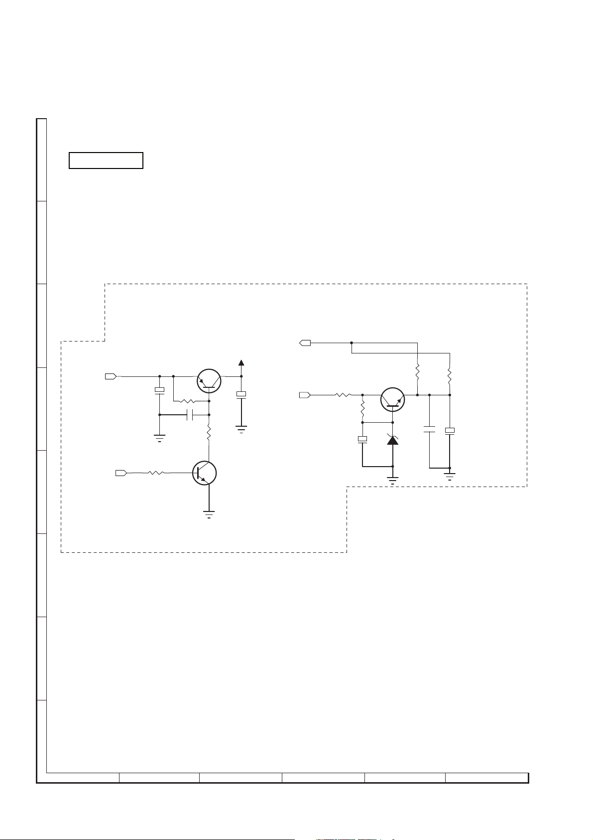
Figure 5-10: MAIN (TUNER AUDIO AND MUTE) SCHEMATIC DIAGRAM
5 – 12
Page 25

-MEMO-
XL-DH20NH
5 – 13
Page 26

XL-DH20NH
0
F
2
2
1
u
6
K
A
B
C
D
E
F
G
POWER / AMPLIFIER PWB-B
HV300V
BR201
KDL460
1 2
1 2
CX202
0.22uF/275V
R29
3
4
432
R201
3
3
4
4
TVR1
1
12
14471
F201
T2.5A L250V
1
1
CN302
AC IN
R32
R202
1M/SMD
2
2
1 2
1 2
1M/SMD
1
1
2
CY201
102P/250V
!
AC1 AC2
1M/SMD
LF201
UF16/35mH
0.22uF/275V
1M/SMD
LF202
EE25/45mH
1
12
2
L
When Servicing, pay attention as the
area enclosed by this line( )
is directly connected with AC main
voltage.
1
2
1
2
2
N
EC201
100uF/400V
!
CY202
102P/250V
!
CX201
RT1
5D-9
12
1 2
+
!
EC203
2.2uF/50V
FA
C223
0.1uF
R330 5.1R/SMD
C229
0.1uF
C211
0.1uF
5VB
L206
20uH/2.5A
2200uF/35V
C219
0.1uF
2200uF/35V
L205
20uH/2.5A
+VCC
-VCC
2
3
1
R235
10K
220uF/35V
L203
100uH/1A
20uH/2A
EC218
EC220
5VB
R216
10K
Q220
8050
1
EC207
L204
2
Q201
8050
R214
10K
2
ZD201
12V/1W
+
+
3
R217
10K
470uF/25V
+
1000uF/16V
R215
2K
+
R219
10K
-VEE
+
EC210
EC213
STY
FA
FB
C4
0.1uF
C5
0.1uF
FB
-VCC
+VCC
C208
47K
Q20
3
855
1
8
Q
C21
0.1u
C2
0.1
R2
10
!
T201
EEL19
10
D207
FR107
ZD205
15V/NC
E213
100K
ZD208
22V/NC
D206
FR107
!
!
D208
FR107
103P/1KV
2
1
!
9
8
11
7
12
13
1
C204
2
3
4
+
47uF/50V
4
3
T202
EI33
EC204
10
9
8
11
7
12
13
U204
PC817
1
2
3
4
3
CY203
U206
PC817
4
102P/250V
102P/
250V
13
12
11
9
1
2
CY1
R212
4.7R
ZD206
22V
EC202
C221
0.1uF
R208
0R
2
D205
FR107
6
7
8
1
VCC
1
2
Drain
Drain
Drain
R210
100K/1W
13
R28
560
C201
102P/1KV
2
1
FB201 FB
+
EC214
47uF/50V
ZD2
5.1V/NC
HV300V
FB202
FB
C331
100P/1KV
C232
473P
R205
100K/1W
R204
10K
U201
5
4
Vstr
nc
PWM
R1
NC
3
Vfb
GND
Vcc
2
DM311
ZD203
15V(NC)
3
5
+
C205
0.1uF
R207
4.7R
+
C202
47uF/50V
0.1uF
C203
333P
R209
27K
U202
7M0880
Drain
VCC
PWM
Start
GND
FB
4
ZD207
3V3
Q5
2SC8550
Vce=50v
Ice=500mA
2
2
1
1
3
3
4
4
5
5
6
6
1
1
2
23
!
13
R241
R27
12
11
9
R243
1
23
D209
FR107
EC205
220uF/35V
D210
FR107
D211
FR107
D212
FR107
D214
SR360
C222
102P/1KV
R326
330R
R327
1K
2
3
U203
TL431
1
D215A/B UF5404X2
C215
47/SMD
102P/1KV
47/SMD
EC217
2200uF/35V
EC219
2200uF/35V
R30
C218
47/SMD
R242
47/SMD
102P/1KV
D216A/B
UF5404X2
ZD4
18V
1K
R244
10K
C221
0.1uF
3
U205
TL431
1
VCC
U207
PC817
4
4
3
3
!
+
R221 2K/SMD
R31 2K/SMD
2
+
220uF/35V
1
+
EC209
470uF/25V
EC212
+
1000uF/16V
R248
5R1/SMD
R239
C213
0.1uF
+
+
R245
68K
R246
10K
R247
4.7K
R23
330
1
1
2
2
3
1
EC206
1K
C216
0.1uF
R238
10K
R240
10K
Q221
8050
H
1
23456
Figure 5-11: POWER / AMPLIFIER SCHEMATIC DIAGRAM (1/2)
5 – 14
Page 27

XL-DH20NH
01
50
ZD201
12V/1W
MD
7
5V
FA
3
R217
10K
R219
10K
FB
-VEE
+
+
EC210
470uF/25V
EC213
+
1000uF/16V
C4
0.1uF
C5
0.1uF
-VCC
+VCC
FA
FB
C208
47K
3
Q202
8550
2
1 3
8550
Q204
C210
0.1uF
C212
0.1uF
R26
10K
-12V
CON2
GND
+12V
GND
DVD5V
DVD5V
GND
STY
AMUTE
FB
GND
TO
6
6
1
FB2
2
BEAD
3
FB1
4
BEAD
Speaker OUT
10K
Q205
8550
1 3
3
R223
1K
2
AMP-R
AMP-L
+12V
2
Q203
8550
1
-12V
EC208
ZD202
+
220uF25V
12V
+12V
+
EC211
47UF/25V
D213
IN4148
R225 560R
+5V
Q212
8050
R256
4K7
+
EC216
100uF/16V
R255
2K
R257
2
1 3
+
-
-
+
MUTE
5
STY
2K
R307
10K/NC
+VCC
HEADPHONES PWB-D
3
+VCC
OUTL
IN-L
IN-R
OUTR
-VCC
-VCC
1
6
-VCC
C1
TO earphone
0.1uF
R4
4.7R
4
R17
18K
R18
560R
8
10
R19
560R
R16
18K
2
R5
4.7R
C2
0.1uF
12345
12345
Q206
2
8050
R227
1 3
10K
U702
TDA72669A
R21
4K7
4K7
R15
EC214
7
+
IN1
1uF/25V
R20
C3
681P
47K
9
GND
R14
C6
681P
47K
EC215
11
+
1uF/25V
IN2
MUTE
R22
10K
1
R219
R220
10K
2
-VEE
R224
5K1
DVD5V
SP1
GND
L
GND
R
AMP-R
FGND
AMP-L
1
2
3
4
5
6
7
8
9
TO MPEG
CON203
-FAF
1
F+
2
FGND
3
-24V-VEE
4
To Front PCB
CON1
1
2
3
TO MPEG
CON201
EC221 22uF/25V
VCC MUTE
D1
R10
IN4148
100K
R6
1
47K
+
EC4
47uF/25V
R215
2K
STY
14
K
EC3
220uF/25V
7
R9
47K
R34
47K
D2
R8 1K
IN4148
R11
1K
A_MUTE
Q2
8550
2 3
D10
IN4148
+
ZD3
16V
8 9 10 11 12
+
R13
15K
Q4
1
8050
2 3
1
Q3
8050
R33
470
R12
10K
2 3
VCC
Figure 5-12: POWER / AMPLIFIER SCHEMATIC DIAGRAM (2/2)
5 – 15
Page 28

XL-DH20NH
DISPLAY PWB-C
A
B
0.1uF
C
D
E
0.1
0.002
STAND-BY
0.002
FUNCTION
0.002
0.002
PLAY/PAUSE
F
G
H
1
23456
Figure 5-13: DISPLAY SCHEMATIC DIAGRAM (1/2)
5 – 16
Page 29

FL DISPLAY
XL-DH20NH
0.1
7
8 9 10 11 12
Figure 5-14: DISPLAY SCHEMATIC DIAGRAM (2/2)
5 – 17
Page 30

XL-DH20NH
A
B
HEADPHONE PWB-D
1NC
1
1
2
C
TO
POWER /
AMPLIFIER PWB
2
3
3
4
4
5
5
6
6
NI
R
D
NG
NIL
TUOR
DNG
OL
TU
1
C
1
R
Fu1.0
H
R074
0742R
HR
1
-
R
L-
1
2
2
3
3
4
4
5
5
6
6
7
7
8
8
9
9
01
01
11
11
HEADPHONE IN
D
E
USB PWB-E
F
FROM
USB EXTERNAL
DEVICE
G
H
1
1234
1234
TO
MAIN PWB
USB 1
23456
Figure 5-15: HEADPHONE AND USB SCHEMATIC DIAGRAM
5 – 18
CN1
Page 31

-MEMO-
XL-DH20NH
5 – 19
Page 32

XL-DH20NH
N
M
A
B
C
D
E
iPod PWB-F
CN1
iPod-CON
3137
32
33
34
35
36
D_GND
D_GND
PWR+5V
PWR-
PWR+
D_GND
D_GND
RXD
TXD
D_GND
VIDE_O
L_CH
R_CH
A_GND
DET
1
2
3
4
5
6
7
8
9
10
11
12
13
14
15
16
17
18
19
20
21
22
23
24
25
26
27
28
29
30
R761
75K 1%
R78
R83`
0R
549K 1%
R79
R80
R81
NC
MA111
R77
75K 1%
C40
FB1`
100R
1UF/50V
D28
D27MA111
1000RH
100R
iPod_L
iPod_R
iPod_GND
D_GND
100K 1%
R72`
100K 1%
R73`
R74`
R75` 100K 1%
100K 1%
D30
MA111
iPod_VIDEO
GND
GND
AGND
D29
MA111
C44
0.1UF
EC29
47UF/16V
iPod_VIDEO
C34
R90
75R/NC
100P
GND
RXD
TXD iPod-DET
iPod_LOUT
iPod_AGND
iPod_ROUT
iPod CON
L25
1.8UH
D11
GND GND
GND
EC42
47UF/10V
FB39
AGND
iPod+5V
C1
100P
1000RH
VIDE
iPod+3V3
R087
R06822R
R069
0R
R071
10K
R070
10K
FB16
F
16
17
18
19
1
2
3
4
5
MODE1
REST
VCC
678
20
15
14
MODEO
13
I2C_SDA
12
I2C_SCL
9
VSS
10
22R
11
U12
R072
1K
G
47UF/10V
10K/NC
R073
104P
C28
EC65
iPod_RST
iPod-SDA
FB
I2C/CLK
H
GND
1
23456
iPod hardware
Figure 5-16: iPod CONNECT AND iPod HARDWARE SCHEMATIC DIAGRAM (1/2)
5 – 20
Page 33

XL-DH20NH
F
CONNECT
VIDEO_OUT
C1
100P
GND
MVCC
B39
1000RH
/10V
iPod+5V
<iPod NOISE>
iPod_R
iPod_GND
iPod_L
iPod_R13100K
100K
iPod_R12
iPod_C11
iPod_E2
100P
iPod_C9
100P
iPod_C12
2.2UF/10V
2.2UF/10V
2.2UF/10V
iPod_C10
iPod_U1
BT606
GND
iPod_C6
iPod_ROUT
iPod_AGND
iPod_LOUT
iPod_R11
2.2UF/10V
1UF/16V
iPod_E9
iPod_C13
2.2UF/10V
5
6
7
IN2
3
VM2
IN14GND
OUT2
VM1
2
8
1
VCC
OUT1
iPod_C7
GND
100
1UF/10V
+12V
NOTE:E2:E9=2:1_capability
GND
102P
C014
R083 30K
10K
10K
C069
R085 30K
102P
GND
iPod-L
iPod-R
AGND
iPod_VCC
1000RH
300RH
300RH
300RH
300RH
300RH
FB47
FB14
FB13
FB12
FB29
FB31
GND
GND
AGND
iPod_DET
iPod_RXD
iPod_TXD
R084
R086
iPod_VIDEO
1
2
3
4
5
6
7
8
9
10
11
CN2
CON 2.0mm(1x11)/iPod
1
2
3
4
5
6
7
8
9
10
11
CON8
CON 2.0mm(1x11)/iPod
7
8 9 10 11 12
Figure 5-17: iPod CONNECT AND iPod HARDWARE SCHEMATIC DIAGRAM (2/2)
5 – 21
Page 34

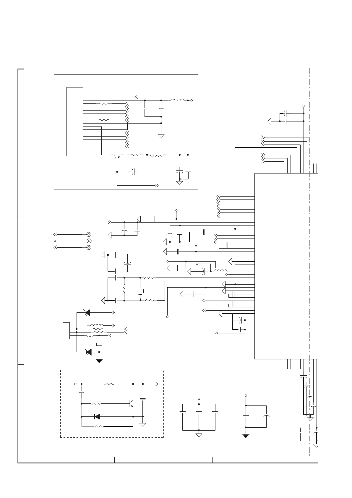
XL-DH20NH
A
RCH
[4] Charts Of Connecting Wires
A
CNS2
10987654321
RING CORE
(2 TURNS)
CN2
10987654321
B
ANTENNA
AUX IN
C
AM LOOP
FM
VIDEO OUT
L-CH
D
E
F
G
H
FROM
iPod EXTERNAL
DEVICE
CN1
130
iPod PWB-F
TOP VIEW
CN2
FOR MICOM
REFLASH ONLY
1234
CON7
RING CORE
(2 TURNS)
1234567891011
1234567891011
CNS2
CON11
1234567891011
CON8
1234
56789
1234
CON9
10
1234
CNS9
BKBKBK
BK
1
234
CN1
123456789
CON13
USB1
FOR
USB EXTERN
DEVICE
1
23456
Figure 5-18: WIRING CONNECTION (1/2)
5 – 22
Page 35

XL-DH20NH
L-CH
DISPLAY PWB-C
TOP VIEW
CNS302
BR
BR
AC POWER SUPPLY CORD
CN1
1234
NL
CN302
POWER / AMPLIFIER PWB-D
TOP VIEW
AUX IN
R-CH
123456789
CNS201-B
1
123
23
BK
BK
BK
BK
BK
BK
BK
BK
BK
WH
BK
RD
CNS1
1234
1234
56789
123
CNS201-A
CON203
1234
123456
789
CON201
123
CON1
123
SP1
CON2
456
56789
FOR
USB EXTERNAL
DEVICE
13 11 9 5 173
15
CON1
CON2
CON5
MAIN PWB-A
TOP VIEW
CON2
14
16 12 10 6 284
123 546
123 546
CNS1-B
116
CNS2-A
123 546
123 54
CNS5-A
FFC1
116
TO
CD PICK UP UNIT
CNS1-A
CNS1
123
123
CN1
456
BKBKBKBKBK
456
R-CH
BK
SPEAKER
TERMINAL
HEADPHONE PWB-D
L-CH
TOP VIEW
CNS2-B
BK
BK
BK
BK
BK
BK
123 546
BK
BK
BK
BK
BK
123 54
CNS5-B
TO
CD MOTOR PWB
TO
CD MECHANISM
PHONES IN
COLOR TABLE
WH
WHITE
RD
RED
BLACK
BK
BROWN
BR
7
8 9 10 11 12
Figure 5-19: WIRING CONNECTION (2/2)
5 – 23
Page 36

XL-DH20NH
[5] Wiring Side Of PWB
A
MAIN PWB-A
B
AM LOOP
ANTENNA
FM
75 OHMS
C
D
1234
E
F
10 11
23456 789
1
G
Lead-free solder indication
Lead-free solder is used in the MAIN PWB.
Refer to "Precautions for handling lead-free solder" for instructions
and precautions.
H
1
23456
Figure 5-20: WIRING SIDE OF MAIN PWB (TOP VIEW) (1/2)
1 2 34 5678910 12
5 – 24
Page 37

AUX IN
VIDEO OUTPUT L-CH R-CH
XL-DH20NH
32 1
1234
1234567 89
13579
111315
2468
10121416
5 432 1 564321
7
8 9 10 11 12
Figure 5-21: WIRING SIDE OF MAIN PWB (TOP VIEW) (2/2)
5 – 25
Page 38

XL-DH20NH
A
MAIN PWB-A
B
C
D
E
F
G
H
1
23456
Figure 5-22: WIRING SIDE OF MAIN PWB (BOTTOM VIEW) (1/2)
5 – 26
Page 39

XL-DH20NH
7
8 9 10 11 12
Figure 5-23: WIRING SIDE OF MAIN PWB (BOTTOM VIEW) (2/2)
5 – 27
Page 40

XL-DH20NH
POWER / AMPLIFIER PWB-B
A
SPEAKER TERMINAL
L-CH R-CH
B
1 2345 6
C
BCE
BCE
BCE
123
BCE
BCE
BCE
BCE
BCE
BCE
BCE
1 23456 7 89
BCE
23 4
1
BCE
D
BCE
BCE
E
F
G
Lead-free solder indication
Lead-free solder is used in the POWER PWB.
Refer to "Precautions for handling lead-free solder" for instructions
H
and precautions.
1
23456
Figure 5-24: WIRING SIDE OF POWER / AMPLIFIER PWB (TOP VIEW)
BCE
When Servicing, pay attention as the
area enclosed by this line( )
is directly connected with AC main
voltage.
5 – 28
Page 41

XL-DH20NH
A
B
C
D
POWER / AMPLIFIER PWB-B
E
F
area enclosed by this line( )
When Servicing, pay attention as the
is directly connected with AC main
voltage.
G
H
1
23456
Figure 5-25: WIRING SIDE OF POWER / AMPLIFIER PWB (BOTTOM VIEW)
5 – 29
Page 42

XL-DH20NH
A
DISPLAY PWB-C
B
C
D
E
12345678910
RED
BCE
ON/
STAND-BY
F
FUNCTION
G
Lead-free solder indication
H
Lead-free solder is used in the DISPLAY PWB.
Refer to "Precautions for handling lead-free solder" for instructions
and precautions.
1
23456
Figure 5-26: WIRING SIDE OF DISPLAY PWB (TOP VIEW) (1/2)
5 – 30
Page 43

XL-DH20NH
ECB
123 4
PLAY/
PAUS E
OPEN/
CLOSE
7
8 9 10 11 12
Figure 5-27: WIRING SIDE OF DISPLAY PWB (TOP VIEW) (2/2)
5 – 31
Page 44

XL-DH20NH
A
DISPLAY PWB-C
B
PT6311
C
U1
D
E
F
WIRE 1
G
Lead-free solder indication
H
Lead-free solder is used in the DISPLAY PWB.
Refer to "Precautions for handling lead-free solder" for instructions
and precautions.
1
23456
Figure 5-28: WIRING SIDE OF DISPLAY PWB (BOTTOM VIEW) (1/2)
5 – 32
Page 45

XL-DH20NH
7
8 9 10 11 12
Figure 5-29: WIRING SIDE OF DISPLAY PWB (BOTTOM VIEW) (2/2)
5 – 33
Page 46

XL-DH20NH
A
HEADPHONE PWB-D
B
C
D
E
USB PWB-E
HEADPHONE IN
USB IN
Top view
123456
C1
TO
ROHS
CHASSIS
F
1234
G
Top view
Lead-free solder indication
H
Lead-free solder is used in the HEADPHONE & USB PWB.
Refer to "Precautions for handling lead-free solder" for instructions
and precautions.
1
23456
Figure 5-30: WIRING SIDE OF HEADPHONE AND USB PWB
5 – 34
Bottom View
Page 47

A
B
C
XL-DH20NH
iPod PWB-F
1234567891011
D
FROM
E
F
iPod EXTERNAL DEVICE
G
Lead-free solder indication
H
Lead-free solder is used in the iPod PWB.
Refer to "Precautions for handling lead-free solder" for instructions
and precautions.
1
23456
Figure 5-31: WIRING SIDE OF iPod PWB
5 – 35
Page 48

XL-DH20NH
CHAPTER 6. FLOWCHART
[1] Troubleshooting
1. When the CD does not function
The CD section may not operate when the objective lens of the optical pickup is dirty. Clean the objective lens, and
check the playback operation. When this section does not operate even after the above step is taken, check the following items.
Remove the cabinet and follow the trouble shooting instructions.
"Track skipping and/or no TOC (Table Of Contents) may be caused by build up of dust other foreign matter on the laser
pickup lens. Before attempting any adjustment make certain that the lens is clean. If not, clean it as mentioned below."
Turn the power off.
Gently clean the lens with a lens cleaning tissue and a small amount of isopropyl alcohol.
Do not touch the lens with the bare hand.
Parts code
1. CD optical pickup Lens cleaner disc UDSKA0004AFZZ
HOW TO USE
Using the brush in the cleaner cap, apply 1 or 2 drops of the cleaning fluid to the
1.
brush on the CD cleaner disc which has the mark next to it.
Place the CD cleaner disc onto the CD disc compartment with the brush side down,
2.
then press the play button.
You will hear music for about 20 seconds and the CD player will automatically stop.
3.
If it still play continuously, press the stop button.
CAUTION
The CD lens cleaner should be effective for 30-50 operations, however if the
brushes become worn out earlier then please replace the cleaner disc.
If the CD cleaner brushes become very wet then wipe off any excess fluid with a soft
cloth.
Do not drink the cleaner fluid or allow it contact with the eyes. In the event of this
happening then drink and / or rinse with clean water and seek medical advice.
The CD cleaner disc must not be used on car CD players or on computer CD-ROM
drives.
All rights reserved. Unauthorized duplicating, broadcasting and renting this product
is prohibited by law.
2. When a CD cannot be played
Cleaning fluid
Cleaner disc
2.1. Pressing the CD operation key is accepted, but playback does not occur.
1) Focus error system check
2) Audio do not operate normally
6 – 1
Page 49

( 1 ) Focus error system check.
Although a CD is inserted and the cover is closed,
" NO DISC " is displayed.
XL-DH20NH
1. Does the servo supply is + 3.3 V?
Yes
2. Is it Open / Close function OK ? No Check incoming power supply VCC ( +3.3V )
Yes
3. Is Sled able to move to inner ? No Check Sled circuit, U304 ( Pin 28 ).
Yes
4. Is the laser lit ? No Check SLE circuit, CD Laser circuits.
Yes
5. Does the focus ( lens ) move up and down ? No Check U302 ( Pin 109, 3 ,4 ) and U304 ( Pin 1, 28 ).
Yes
6. Is the turntable rotating ? No Check U302 ( Pin 2 ) and U304 ( Pin 26 ).
Yes
7. Is it the CD Laser driver circuit OK ? No
No Check incoming jack supply AC ( 220V ).
Check Spindle SLED circuit.
Check the CD Laser driver ( Q206, Q302, Q303 )
peripheral circuit.
( 2 ) Audio do not operate normally
The RF waveform is normal and the time is
displayed normally, but no sound is produced.
Or the sound has dropouts.
1. Put a disc on DISC compartment.
Yes
2. When playback starts does the disc initialise ? No Repeat steps as Focus errror system check occurred.
Yes
3. Are the RF signal level output from U302
pin no 21 and 33 ( 3.3V and 1.8V ) normal?
( Waveform drawing Figure 1 for CD )
Yes
4. Replace Servo PWB. No Replace optical pickup mechanism unit.
Yes
No Is the objective lens of optical pickups clean ?
Yes
6 – 2
Page 50

XL-DH20NH
5. Does the supply shows as + 3.3 V? No Check supply ( Q210 Pin No.1 ).
Yes
6. Is Reset function OK? No Check U302 pin no 102.
( Waveform drawing Figure 3 )
Yes
7. Is clock frequency shows 16.934MHz? No Check clock circuit ( Y301 , C308 , C309 )
Yes
8. Is the Flash is normal? No Check U302 pin no 102.
Yes
9. Is the SDRAM is normal? No Check U303 pin no 35.
Yes
10. Is the DSP is normal? No Check U302 Data Bus.
Yes
11. Is the Audio out is normal? No Check Audio out circuit ( U302 Pin No.35 and 38 )
or at Audio filter U602 circuits.
9
U302 33
RF
Figure 1
10
U302 102
RESET
Figure 2
6 – 3
Page 51

CHAPTER 7. OTHERS
[1] Function Table Of IC
U5 92L117ALIM5601 : Digital Signal Processor ( M5673 ) / ( 1/3 )
XL-DH20NH
I2S
SPDIF
I2C
master/slave
LCD
module
GPIO
SD/MMC
card
MS/MS pro
card
Crystal
16.9344MHz
XTAL
PLL
Interface control logic
CD
servo controller
& decoder
3.3V
ADSP
1.8V
Linear
regulator
MIC in FM in Line in
boost
ADC
DAC MUX
Micro
CD ECC
& System
buffer
Controller
Cache
MUX
L/R Line Out
USB host
controller
USB
transceiver
Motor
driver
Serial
Flash
Pickup
Head
Figure 7-1 BLOCK DIAGRAM OF IC
USB
device
7 – 1
Page 52

XL-DH20NH
[2] VFD Display
VFD1 92L118GTD805A1
GRID ASSIGNMENT
OUTER DIMENSIONS
131
PATTERN AREA
7 – 2
Page 53

PARTS GUIDE
MICRO COMPONENT SYSTEM
XL-DH20NH
[1] INTEGRATED CIRCUITS
[2] TRANSISTORS
[3] DIODES
[4] TRANSFORMER
[5] COILS
[6] VIBRATORS/ CRYSTALS
[7] CAPACITORS
MODEL
XL-DH20NH Micro Component System consisting of
XL-DH20NH (main unit) and CP-DH20NH (speaker system).
CONTENTS
[8] RESISTORS
[9] OTHER CIRCUITRY PARTS
[10] CABINET PARTS/ CD MECHANISM
PARTS
[11] ACCESSORIES/ PACKING PARTS
[12] P.W.B. ASSEMBLY
[13] OTHER SERVICE PARTS
XL-DH20NH
Explanation of PWB Assembly parts code category
S Category -- Repair ( Component parts of PWB can be replace and repair, PWB no supply )
X Category -- Replacement ( PWB can not be repair. Component parts no supply )
S.X Category -- Repair and Replacement ( PWB can repair and replace )
KG Category -- Revolve repair by Business Center ( Return to Business Center and repair by manufacturer. Component parts no supply )
Parts marked with " " are important for maintaining the safety of the set. Be sure to replace these parts with specified
ones for maintaining the safety and performance of the set.
!
SHARP CORPORATION
This document has been published to be used
for after sales service only.
The contents are subject to change without notice.
Page 54

XL-DH20NH
NO. PARTS CODE
PRICE
RANK
[1] INTEGRATED CIRCUITS
IC1 92L11711170332 Voltage Regulator, 3.3V
IC2 92L11711170332 Voltage Regulator, 3.3V
! U1 92L117TDA72652 Power Amplifier, TDA7265B [Use in POWER PWB-B]
! U9 92L117FSDM0565 AM FSDM0565
U1 92L11700045581 AC Operational Amplifier, 4558 [Use in MAIN PWB-A]
U1 92L117CS163111 AH CS16311 [Use in DISPLAY PWB-C]
U1 92L117BT606001 BT606 [Use in iPod PWB-F]
U2 92L117EON2M001 EON 2M FLASH
U3 92L117A5888S01 A5888S
U4 92L117SI473101 SI4731
U5 92L117ALIM5601 ALIM5673
U6 92L117RF212662 RF21266
U7 92L11724C02001 24C02
U8 92L117NJU73911 NJU7391V
U12 92L117IPOD0001 MFI341S2161
U20 92L117RCR51001 AE RCR5102
U201 92L117DM311D01 DM311
U202 92L1177M088002 7M0880
U203 92L117TL431A03 TL431A
U204 92L114EL817001 AC Photocoupler, EL817
U205 92L117TL431A03 TL431A
U206 92L114EL817001 AC Photocoupler, EL817
U207 92L114EL817001 AC Photocoupler, EL817
[2] TRANSISTORS
Q1 92L11300080502 AB 8050 [Use in MAIN PWB-A]
Q1 92L11300080506 8050 [Use in POWER PWB-B]
Q1 92L11300090144 8050 [Use in DISPLAY PWB-C]
Q2 92L11300039042 AB 3904 [Use in MAIN PWB-A]
Q2 92L11300085509 SS8550 [Use in POWER PWB-B]
Q3 92L11300039062 AB 3906 [Use in MAIN PWB-A]
Q3 92L11300080506 8050 [Use in POWER PWB-B]
Q3 92L11300090144 8050 [Use in DISPLAY PWB-C]
Q4 92L11300080506 8050 [Use in POWER PWB-B]
Q5 92L11300039042 AB 3904 [Use in MAIN PWB-A]
Q5 92L11300085509 SS8550 [Use in POWER PWB-B]
Q6 92L11300085502 AB 8550
Q7 92L11300039042 AB 3904
Q8 92L1132SB77202 2SB772
Q9 92L1132SB77202 2SB772
Q11 92L11300080502 AB 8050
Q12 92L11300039062 AB 3906
Q13 92L11300039042 AB 3904
Q14 92L11300039042 AB 3904
Q15 92L11300039042 AB 3904
Q16 92L1132SB77202 2SB772
Q17 92L11300039042 AB 3904
Q18 92L1132SB11323 2SB1132
Q201 92L11300080506 8050
Q202 92L11300085509 SS8550
Q203 92L11300085509 SS8550
Q204 92L113MPAS4202 MPSA42
Q205 92L11300085509 SS8550
Q206 92L11300080506 8050
Q212 92L11300080506 8050
Q220 92L11300080506 8050
Q221 92L11300080506 8050
[3] DIODES
BR201 92L109KDL40601 KDL406
D1 92L10901N41482 AB 1N4148 [Use in MAIN PWB-A]
D1 92L1091N414802 1N4148 [Use in POWER PWB-B]
D1 92L11103R02002 AB LED, 3mm Red [Use in DISPLAY PWB-C]
D2 92L10901N41482 AB 1N4148 [Use in MAIN PWB-A]
D2 92L1091N414802 1N4148 [Use in POWER PWB-B]
D2 92L11103R06001 LED, 3mm Blue [Use in DISPLAY PWB-C]
D3 92L10901N41482 AB 1N4148 [Use in MAIN PWB-A]
D3 92L10901N41489 1N4148 [Use in POWER PWB-B]
D3 92L11103R06001 LED, 3mm Blue [Use in DISPLAY PWB-C]
D4 92L10901N41482 AB 1N4148 [Use in MAIN PWB-A]
D4 92L11103R06001 LED, 3mm Blue [Use in DISPLAY PWB-C]
D5 92L10901N41482 AB 1N4148
D6 92L10901N41482 AB 1N4148
D7 92L10901N41482 AB 1N4148
D8 92L10901N41482 AB 1N4148
D9 92L11000680054 Zener, 6.8V,1/2W
D10 92L11000680054 Zener, 6.8V,1/2W [Use in MAIN PWB-A]
D10 92L1091N414802 1N4148 [Use in POWER PWB-B]
D11 92L1090BAV99S2 AB BAV99-S
D13 92L109IN539902 1N5399
D14 92L109IN539902 1N5399
D15 92L109IN539902 1N5399
D16 92L10901N41482 AB 1N4148
D17 92L10901N41482 AB 1N4148
D18 92L10901N41482 AB 1N4148
D19 92L10901N41482 AB 1N4148
D205 92L10900FR1071 FR107
NEW
MARK
PAR T
RANK
DESCRIPTION
1
Page 55

NO. PARTS CODE
PRICE
RANK
NEW
MARK
PAR T
RANK
[3] DIODES
D206 92L10900FR1071 FR107
D207 92L10900FR1071 FR107
D208 92L10900FR1071 FR107
D209 92L10900FR1071 FR107
D210 92L10900FR1071 FR107
D211 92L10900FR1071 FR107
D212 92L10900FR1071 FR107
D213 92L1091N414802 1N4148
! D215A 92L109UF540402 UF5404,3A/200V
! D216A 92L109UF540402 UF5404,3A/200V
! D215B 92L109UF540402 UF5404,3A/200V
! D216B 92L109UF540402 UF5404,3A/200V
D214 92L10900SB3602 AE SB360
Z1 92L11000390051 AC Zener, 3.9V,1/2W
ZD1 92L11000910052 AB Zener, 9.1V,1/2W [Use in MAIN PWB-A]
ZD1 92L11000510053 Zener, 5.1V,1/2W [Use in POWER PWB-B]
ZD2 92L11000390051 AC Zener, 3.9V,1/2W [Use in MAIN PWB-A]
ZD2 92L11000510053 Zener, 5.1V,1/2W [Use in POWER PWB-B]
ZD3 92L11001500053 Zener, 15V, 1/2W
ZD4 92L11001800053 Zener, 18V, 1/2W
ZD5 92L11001800052 Zener, 18V, 1/2W
ZD201 92L11001200102 Zener, 12V, 1W
ZD202 92L11001200102 Zener, 12V, 1W
ZD206 92L11002200052 Zener, 22V, 1/2W
ZD207 92L11000330052 Zener, 3.3V, 1/2W
[4] TRANSFORMER
! T201 92L108EEL19015 POWER
! T202 92L108EI33N904 SUB
[5] COILS
FB1 92L106S0805K01 Ferrite Bead, 7 ohms [Use in MAIN PWB-A]
FB1 92L10603560002 Bead, 3.5 X 6mm [Use in POWER PWB-B]
FB2 92L106S0603K01 Ferrite Bead, 7 ohms [Use in MAIN PWB-A]
FB2 92L10603560002 Bead, 3.5 X 6mm [Use in POWER PWB-B]
FB3 92L106S0805K01 Ferrite Bead, 7 ohms [Use in MAIN PWB-A]
FB3 92L10603560002 Bead, 3.5 X 6mm [Use in POWER PWB-B]
FB4 92L106S0603K01 Ferrite Bead, 7 ohms [Use in MAIN PWB-A]
FB4 92L10603560002 Bead, 3.5 X 6mm [Use in POWER PWB-B]
FB5 92L106S0603K01 Ferrite Bead, 7 ohms [Use in MAIN PWB-A]
FB5 92L10603560002 Bead, 3.5 X 6mm [Use in POWER PWB-B]
FB6 92L106S0603K01 Ferrite Bead, 7 ohms
FB7 92L106S0603K01 Ferrite Bead, 7 ohms
FB9 92L106S0603K01 Ferrite Bead, 7 ohms
FB12 92L106S0603K01 Ferrite Bead, 7 ohms
FB13 92L106S0603K01 Ferrite Bead, 7 ohms
FB14 92L106S0603K01 Ferrite Bead, 7 ohms
FB16 92L106S0603K01 Ferrite Bead, 7 ohms
FB17 92L106S0603K01 Ferrite Bead, 7 ohms
FB21 92L106S0603K01 Ferrite Bead, 7 ohms
FB22 92L106S0603K01 Ferrite Bead, 7 ohms
FB23 92L106S0603K01 Ferrite Bead, 7 ohms
FB24 92L106S0603K01 Ferrite Bead, 7 ohms
FB26 92L106S0603K01 Ferrite Bead, 7 ohms
FB29 92L106S0603K01 Ferrite Bead, 7 ohms
FB31 92L106S0603K01 Ferrite Bead, 7 ohms
FB38 92L106S0603K01 Ferrite Bead, 7 ohms
FB39 92L106S0603K01 Ferrite Bead, 7 ohms
FB40 92L106S0805K01 Ferrite Bead, 7 ohms
FB44 92L106S0805K01 Ferrite Bead, 7 ohms
FB45 92L106S0805K01 Ferrite Bead, 7 ohms
FB47 92L106S0805K01 Ferrite Bead, 7 ohms
FB51 92L106S0805K01 Ferrite Bead, 7 ohms
FB59 92L106S0805K01 Ferrite Bead, 7 ohms
FB61 92L106S0805K01 Ferrite Bead, 7 ohms
L1 92L105101K0001 100 µH[Use in MAIN PWB-A]
L1 92L106S0603K01 Ferrite Bead, 7 ohms [Use in iPod PWB-F]
L2 92L106S0805K01 Ferrite Bead, 7 ohms
L7 92L106S0603K01 Ferrite Bead, 7 ohms
L9 92L105101K0001 100 µH
L10 92L106S0603K01 Ferrite Bead, 7 ohms
L14 92L106S0603K01 Ferrite Bead, 7 ohms
L15 92L106S0805K01 Ferrite Bead, 7 ohms
L16 92L106S0805K01 Ferrite Bead, 7 ohms
L17 92L106S0805K01 Ferrite Bead, 7 ohms
L18 92L106S0805K01 Ferrite Bead, 7 ohms
L19 92L106S0603K01 Ferrite Bead, 7 ohms
L22 92L106S0805K01 Ferrite Bead, 7 ohms
L25 92L1051R8K0003 Coil 1.8 µH
L41 92L105271K0001 Inductance, 270 nH
L42 92L106S0603K01 Ferrite Bead, 7 ohms
L44 92L106S0603K01
L45 92L106S0603K01 Ferrite Bead, 7 ohms
L46 92L106S0603K01 Ferrite Bead, 7 ohms
L47 92L106S0603K01 Ferrite Bead, 7 ohms
L49 92L106S0603K01 Ferrite Bead, 7 ohms
L50 92L106S0603K01 Ferrite Bead, 7 ohms
L56 92L106S0805K01 Ferrite Bead, 7 ohms
Ferrite Bead, 7 ohms
XL-DH20NH
DESCRIPTION
2
Page 56

XL-DH20NH
NO. PARTS CODE
PRICE
RANK
[5] COILS
L203 92L105101J0001 Coil 100 µH
L204 92L105200L2001 Coil 20 µH
L205 92L105220K7002 Coil 22 µH
! LF201 92L105UM007002 Line Filter
! LF202 92L105EE25002U Line Filter
L206 92L105220K7002 Coil 22 µH
RC1 92L10623061401 Ring Core, 22.5 X 6.4 X 13.8mm [Use in iPod PWB-F]
RC2 92L10623061401 Ring Core, 22.5 X 6.4 X 13.8mm [Use in DISPLAY PWB-C]
RC3 92L10619091301 Ring Core, 19 X 8 X 13mm [Use in POWER PWB-B]
RC4 92L10619091301 Ring Core, 19 X 8 X 13mm [Use in USB PWB-E]
RC5 92L10616081201 Ring Core, 16 X 8 X 12mm
R059 92L106S0805K01 Ferrite Bead, 7 ohms
T1 92L108SL755TF1 AM Coil
[6] VIBRATORS/ CRYSTALS
X1 92L12732768205 Crystal, 32.768KHz
X2 92L12732768205 Crystal, 32.768KHz
X3 92L12716920102 AD Crystal, 16.9344MHz
[7] CAPACITORS
C1 92L104101J0601 AB 100 pF 50V [Use in MAIN PWB-A]
C1 92L104104K0802 0.1 µF 100V [Use in POWER PWB-B]
C1 92L104104Z0603 0.1 µF 50V [Use in DISPLAY PWB-C]
C2 92L104104M0601 0.1 µF 50V [Use in MAIN PWB-A]
C2 92L104104K0802 0.1 µF 100V [Use in POWER PWB-B]
C2 92L104101K0603 100 pF 50V [Use in DISPLAY PWB-C]
C3 92L104200J0601 AB 20 pF 50V [Use in MAIN PWB-A]
C3 92L104102M0601 AA 1000 pF 50V [Use in POWER PWB-B]
C3 92L104101K0603 100 pF 50V [Use in DISPLAY PWB-C]
C3 92L104101J0601 AB 100 pF 50V [Use in iPOD PWB-F]
C4 92L104200J0601 AB 20 pF 50V [Use in MAIN PWB-A]
C4 92L104104Z0601 AA 0.1 µF 50V [Use in POWER PWB-B]
C4 92L104101K0603 100 pF 50V [Use in DISPLAY PWB-C]
C5 92L104104M0601 0.1 µF 50V [Use in MAIN PWB-A]
C5 92L104104Z0603 0.1 µF 50V [Use in DISPLAY PWB-C]
C5 92L104102M1602 1000 pF 50V [Use in POWER PWB-B]
C5 92L104101J0601 AB 100 pF 50V [Use in iPOD PWB-F]
C6 92L104220J0601 22 pF 50V [Use in MAIN PWB-B]
C6 92L104102M0601 AA 1000 pF 50V [Use in POWER PWB-B]
C6 92L104104Z0603 0.1 µF 50V [Use in DISPLAY PWB-C]
C6 92L104225Z0301 AE 2.2 µF 50V [Use in iPOD PWB-F]
C7 92L104104K0402 0.1 µF 25V [Use in MAIN PWB-A]
C7 92L104102M1602 1000 pF 50V [Use in POWER PWB-B]
C7 92L104104Z0603 0.1 µF 50V [Use in DISPLAY PWB-C]
C7 92L104105Z0301 AA 1 µF 16V [Use in iPOD PWB-F]
C8 92L104224Z0402 0.22 µF 25V
C9 92L104330J0601 33 pF 50V [Use in MAIN PWB-A]
C9 92L104104Z0602 0.1 µF 50V [Use in POWER PWB-B]
C9 92L104101J0601 AB 100 pF 50V [Use in iPOD PWB-F]
C10 92L104330J0601 33 pF 50V [Use in MAIN PWB-A]
C10 92L104102M1904 1000 pF 1KV [Use in POWER PWB-B]
C10 92L104225Z0301 AE 2.2 µF 50V [Use in iPOD PWB-F]
C11 92L104104M0601 0.1 µF 50V [Use in MAIN PWB-A]
C11 92L104102M1904 1000 pF 1KV [Use in POWER PWB-B]
C11 92L104225Z0301 AE 2.2 µF 50V [Use in iPOD PWB-F]
C12 92L104225M0601 2.2 µF 50V [Use in MAIN PWB-A]
C12 92L104104Z0602 0.1 µF 50V [Use in POWER PWB-B]
C12 92L104101J0601 AB 100 pF 50V [Use in iPOD PWB-F]
C13 92L104225M0302 2.2 µF 16V, Electrolytic [Use in MAIN PWB-A]
C13 92L104104Z0602 0.1 µF 50V [Use in POWER PWB-B]
C13 92L104225Z0301 AE 2.2 µF 50V [Use in iPOD PWB-F]
C14 92L104225M0302 2.2 µF 16V, Electrolytic
C15 92L104225M0302 2.2 µF 16V, Electrolytic
C16 92L104225M0302 2.2 µF 16V, Electrolytic
C17 92L104225M0302 2.2 µF 16V, Electrolytic
C18 92L104225M0302 2.2 µF 16V, Electrolytic
C19 92L104682K0601 6800 pF 50V
C20 92L104473K0803 0.047 µF 100V [Use in POWER PWB-B]
C20 92L104472K0601 4700 pF 50V [Use in DISPLAY PWB-C]
C21 92L104225M0601 2.2 µF 50V [Use in MAIN PWB-A]
C21 92L104473K0803
C22 92L104682K0601 6800 pF 50V
C23 92L104104K0402 0.1 µF 25V
C24 92L104224Z0402 0.22 µF 25V
C25 92L104472K0601 4700 pF 50V
C26 92L104225M0302 2.2 µF 16V, Electrolytic
C27 92L104476M0306 47 µF 16V, Electrolytic
C28 92L104104M0601 0.1 µF 50V
C29 92L104102K0601 AB 1000 pF 50V
C30 92L104102K0601 AB 1000 pF 50V
C31 92L104225M0302 2.2 µF 16V, Electrolytic
C32 92L104225M0302 2.2 µF 16V, Electrolytic
C33 92L104225M0302 2.2 µF 16V, Electrolytic
C34 92L104101J0601 AB 100 pF 50V
C35 92L104103K0601 AA 0.01 µF 50V
C36 92L104107M030G 100 µF 16V, Electrolytic
C37 92L104104M0602 0.1 µF 50V
C46 92L104104M0601 0.1 µF 50V
NEW
MARK
PAR T
RANK
0.047 µF 100V [Use in POWER PWB-B]
3
DESCRIPTION
Page 57

NO. PARTS CODE
PRICE
RANK
NEW
MARK
PAR T
RANK
[7] CAPACITORS
C48 92L104104M0601 0.1 µF 50V
C62 92L104104M0602 0.1 µF 50V
C69 92L104104M0602 0.1 µF 50V
C78 92L104101J0601 AB 100 pF 50V
C79 92L104474Z0301 AB 0.47 µF 16V
C80 92L104225M0302 2.2 µF 16V, Electrolytic
C81 92L104225M0302 2.2 µF 16V, Electrolytic
C82 92L104200J0601 AB 20 pF 50V
C83 92L104200J0601 AB 20 pF 50V
C84 92L104104M0602 0.1 µF 50V
C87 92L104104M0602 0.1 µF 50V
C88 92L104104M0602 0.1 µF 50V
C89 92L104104M0602 0.1 µF 50V
C92 92L104225M0302 2.2 µF 16V, Electrolytic
C96 92L104104M0602 0.1 µF 50V
C98 92L104104M0602 0.1 µF 50V
C201 92L104102M1902 1000 pF 1KV
C202 92L104104Z0602 0.1 µF 50V
C203 92L104333K0801 0.033 µF 100V
C204 92L104103Z1902 0.01 µF 1KV
C205 92L104104Z0602 0.1 µF 50V
C206 92L104104K0802 0.1 µF 100V
C208 92L104104Z0602 AB 0.1 µF 50V
C209 92L104104Z0601 AA 0.1 µF 50V
C210 92L104104Z0601 AA 0.1 µF 50V
C211 92L104104Z0601 AA 0.1 µF 50V
C212 92L104104Z0601 AA 0.1 µF 50V
C213 92L104104K0802 0.1 µF 100V
C215 92L104102M1902 1000 pF 1KV
C216 92L104104Z0602 AB 0.1 µF 50V
C218 92L104102M1902 1000 pF 1KV
C219 92L104104Z0601 AA 0.1 µF 50V
C221 92L104104K0802 0.1 µF 100V
C222 92L104102M1902 1000 pF 1KV
C223 92L104104Z0601 AA 0.1 µF 50V
C232 92L104473K0802 0.047 µF 100V
C311 92L104101K1902 100 pF 1KV
! CX201 92L104224Z1302 0.22 µF 275V (X2 Capacitor)
! CX202 92L104224Z1302 0.22 µF 275V (X2 Capacitor)
! CY1 92L104102M1401 1000 pF 400V (Y Capacitor)
! CY201 92L104102M1401 1000 pF 400V (Y Capacitor)
! CY202 92L104102M1401 1000 pF 400V (Y Capacitor)
! CY203 92L104102M1401 1000 pF 400V (Y Capacitor)
C001 92L104474Z0301 AB 0.47 µF 16V
C05 92L104102K0601 AB 1000 pF 50V
C06 92L104820J0601 AA 82 pF 50V
C07 92L104820J0601 AA 82 pF 50V
C08 92L104102K0601 AB 1000 pF 50V
C014 92L104102K0601 AB 1000 pF 50V
C016 92L104104M0601 0.1 µF 50V
C017 92L104104M0601
C018 92L104104M0601 0.1 µF 50V
C019 92L104473M0601 AB 0.047 µF 50V
C020 92L104103K0601 AA 0.01 µF 50V
C021 92L104103K0601 AA 0.01 µF 50V
C022 92L104104M0601 0.1 µF 50V
C023 92L104104M0602 0.1 µF 50V
C024 92L104104M0601 0.1 µF 50V
C025 92L104104M0601 0.1 µF 50V
C026 92L104104M0601 0.1 µF 50V
C027 92L104104M0601 0.1 µF 50V
C028 92L104104M0601 0.1 µF 50V
C029 92L104104M0601 0.1 µF 50V
C030 92L104104M0601 0.1 µF 50V
C031 92L104105Z0301 AA 1 µF 16V
C032 92L104104M0601 0.1 µF 50V
C033 92L104104M0601 0.1 µF 50V
C034 92L104300J0601 AA 30 pF 50V
C035 92L104300J0601 AA 30 pF 50V
C037 92L104104M0601 0.1 µF 50V
C039 92L104104M0601 0.1 µF 50V
C040 92L104104M0601 0.1 µF 50V
C041 92L104823M0602 0.082 µF 50V
C042 92L104823M0602 0.082 µF 50V
C043 92L104104M0601 0.1 µF 50V
C045 92L104104M0601 0.1 µF 50V
C046 92L104104M0601 0.1 µF 50V
C049 92L104104M0601 0.1 µF 50V
C050 92L104104M0601 0.1 µF 50V
C051 92L104104M0601 0.1 µF 50V
C052 92L104104M0601 0.1 µF 50V
C053 92L104104M0601 0.1 µF 50V
C054 92L104104M0601 0.1 µF 50V
C055 92L104104M0601 0.1 µF 50V
C057 92L104104M0601 0.1 µF 50V
C059 92L104104M0601 0.1 µF 50V
C060 92L104104M0601 0.1 µF 50V
C061 92L104104M0601 0.1 µF 50V
C063 92L104104M0602 0.1 µF 50V
0.1 µF 50V
4
XL-DH20NH
DESCRIPTION
Page 58

XL-DH20NH
NO. PARTS CODE
PRICE
RANK
[7] CAPACITORS
C065 92L104104M0602 0.1 µF 50V
C069 92L104102K0601 AB 1000 pF 50V
C070 92L104225M0302 2.2 µF 16V, Electrolytic
C071 92L104104M0602 0.1 µF 50V
C073 92L104102K0601 AB 1000 pF 50V
C074 92L104102K0601 AB 1000 pF 50V
E1 92L104107M030G 100 µF 16V, Electrolytic
E2 92L104107M030G 100 µF 16V, Electrolytic [Use in DISPLAY PWB-C]
E2 92L104226M0307 AA 22 µF 16V, Electrolytic [Use in iPOD PWB-F]
E5 92L104107M030G 100 µF 16V, Electrolytic
E8 92L104107M030G 100 µF 16V, Electrolytic
E9 92L104106M0403 AA 10 µF 25V, Electrolytic
EC1 92L104476M0306 47 µF 16V, Electrolytic
EC2 92L104476M0306 47 µF 16V, Electrolytic
EC3 92L104107M030G 100 µF 16V, Electrolytic [Use in MAIN PWB-A]
EC3 92L104227M0502 220 µF 35V, Electrolytic [Use in POWER PWB-B]
EC4 92L104107M030G 100 µF 16V, Electrolytic [Use in MAIN PWB-A]
EC4 92L104476M0401 47 µF 25V, Electrolytic [Use in POWER PWB-B]
EC5 92L104476M0306 47 µF 16V, Electrolytic
EC6 92L104106M0410 10 µF 25V, Electrolytic
EC7 92L104225M0302 2.2 µF 16V, Electrolytic
EC8 92L104106M0410 10 µF 25V, Electrolytic
EC9 92L104476M0306 47 µF 16V, Electrolytic
EC10 92L104107M030G 100 µF 16V, Electrolytic
EC11 92L104106M0410 10 µF 25V, Electrolytic
EC12 92L104107M030G 100 µF 16V, Electrolytic
EC13 92L104227M0204 220 µF 10V, Electrolytic
EC14 92L104227M0204 220 µF 10V, Electrolytic
EC15 92L104227M0204 220 µF 10V, Electrolytic
EC16 92L104106M0410 10 µF 25V, Electrolytic
EC17 92L104105Z0301 AA 1 µF 16V
EC18 92L104105Z0301 AA 1 µF 16V
EC19 92L104105Z0301 AA 1 µF 16V
EC20 92L104105Z0301 AA 1 µF 16V
EC22 92L104106M0410 10 µF 25V, Electrolytic
EC23 92L104107M030G 100 µF 16V, Electrolytic
EC24 92L104225M0302 2.2 µF 16V, Electrolytic
EC25 92L104107M030G 100 µF 16V, Electrolytic
EC26 92L104107M030G 100 µF 16V, Electrolytic
EC27 92L104477M0207 470 µF 10V, Electrolytic
EC28 92L104107M030G 100 µF 16V, Electrolytic
EC29 92L104476M0306 47 µF 16V, Electrolytic
EC30 92L104476M0306 47 µF 16V, Electrolytic
EC31 92L104106M0410 10 µF 25V, Electrolytic
EC32 92L104107M030G 100 µF 16V, Electrolytic
EC33 92L104476M0306 47 µF 16V, Electrolytic
EC34 92L104107M030G 100 µF 16V, Electrolytic
EC35 92L104477M0207 470 µF 10V, Electrolytic
EC36 92L104227M0204 220 µF 10V, Electrolytic
EC38 92L104227M0204 220 µF 10V, Electrolytic
EC39 92L104107M030G
EC40 92L104476M0306 47 µF 16V, Electrolytic
EC41 92L104476M0306 47 µF 16V, Electrolytic
EC42 92L104476M0306 47 µF 16V, Electrolytic
EC43 92L104107M030G 100 µF 16V, Electrolytic
EC62 92L104107M030G 100 µF 16V, Electrolytic
EC63 92L104106M0410 10 µF 25V, Electrolytic
EC64 92L104475M0610 4.7 µF 50V, Electrolytic
EC65 92L104476M0306 47 µF 16V, Electrolytic
! EC201 92L104107M1401 100 µF 400V, Electrolytic
EC202 92L104476M0604 47 µF 50V, Electrolytic
EC203 92L104225M0605 2.2 µF 50V, Electrolytic
EC204 92L104476M0604 47 µF 50V, Electrolytic
EC205 92L104227M0502 220 µF 35V, Electrolytic
EC206 92L104227M0502 220 µF 35V, Electrolytic
EC207 92L104227M0502 220 µF 35V, Electrolytic
EC208 92L104227M040A 220 µF 25V, Electrolytic
EC209 92L104477M0404 470 µF 25V, Electrolytic
EC210 92L104477M0404 470 µF 25V, Electrolytic
EC211 92L104476M0401 47 µF 25V, Electrolytic
EC212 92L104108M0308 1000 µF 16V, Electrolytic
EC213 92L104108M0308 1000 µF 16V, Electrolytic
EC214 92L104105M0601 1 µF 50V, Electrolytic
EC215 92L104105M0601 1 µF 50V, Electrolytic
EC216 92L104107M0407 100 µF 25V, Electrolytic
EC217 92L104228M0504 2200 µF 35V, Electrolytic
EC218 92L104228M0504 2200 µF 35V, Electrolytic
EC219 92L104228M0504 2200 µF 35V, Electrolytic
EC220 92L104228M0504 2200 µF 35V, Electrolytic
EC221 92L104226M0605 22 µF 50V, Electrolytic
TP81 92L104228M0201 2200 µF 10V, Electrolytic
[8] RESISTORS
FB2 92L10133R0F021 33 OHM 1/10W
FB8 92L10133R0F021 33 OHM 1/10W
FB10 92L10133R0F021 33 OHM 1/10W
FB15 92L1010000J021 AA 0 OHM 1/10W
FB28 92L10122R0J021 22 OHM 1/10W
NEW
MARK
PAR T
RANK
100 µF 16V, Electrolytic
DESCRIPTION
5
Page 59

NO. PARTS CODE
PRICE
RANK
NEW
MARK
PAR T
RANK
[8] RESISTORS
FB33 92L1010000J021 AA 0 OHM 1/10W
FB34 92L1010000J021 AA 0 OHM 1/10W
FB50 92L1010000J021 AA 0 OHM 1/10W
FB202 92L10133R0F021 33 OHM 1/10W
FB204 92L10133R0F021 33 OHM 1/10W
J1 92L50107500001 Jumper, 7.5mm [Use in POWER PWB-B]
J1 92L50105000001 Jumper, 5mm [Use in HEADPHONE PWB-D]
J2 92L50107500001 Jumper, 7.5mm [Use in POWER PWB-B]
J2 92L50110000001 Jumper, 10mm [Use in DISPLAY PWB-C]
J3 92L50107500001 Jumper, 7.5mm [Use in POWER PWB-B]
J3 92L50110000001 Jumper, 10mm [Use in DISPLAY PWB-C]
J4 92L50110000001 Jumper, 10mm [Use in POWER PWB-B]
J4 92L50110000001 Jumper, 10mm [Use in DISPLAY PWB-C]
J5 92L50110000001 Jumper, 10mm
J6 92L50107500001 Jumper, 7.5mm [Use in POWER PWB-B]
J6 92L50110000001 Jumper, 10mm [Use in DISPLAY PWB-C]
J7 92L50107500001 Jumper, 7.5mm [Use in POWER PWB-B]
J7 92L50110000001 Jumper, 10mm [Use in DISPLAY PWB-C]
J8 92L50107500001 Jumper, 7.5mm [Use in POWER PWB-B]
J8 92L50110000001 Jumper, 10mm [Use in DISPLAY PWB-C]
J9 92L50107500001 Jumper, 7.5mm [Use in POWER PWB-B]
J9 92L50110000001 Jumper, 10mm [Use in DISPLAY PWB-C]
J10 92L50107500001 Jumper, 7.5mm [Use in POWER PWB-B]
J10 92L50110000001 Jumper, 10mm [Use in DISPLAY PWB-C]
J11 92L50112000001 Jumper, 12mm
J12 92L50112000001 Jumper, 12mm
J13 92L50107500001 Jumper, 7.5mm [Use in POWER PWB-B]
J13 92L50110000001 Jumper, 10mm [Use in DISPLAY PWB-C]
J14 92L50110000001 Jumper, 10mm
J15 92L50110000001 Jumper, 10mm
J16 92L50110000001 Jumper, 10mm
J20 92L50107500003 Jumper, 7.5mm [Use in POWER PWB-B]
J22 92L50107500003 Jumper, 7.5mm [Use in POWER PWB-B]
J25 92L50110000003 Jumper, 10mm [Use in POWER PWB-B]
J26 92L50107500003 Jumper, 7.5mm [Use in POWER PWB-B]
J30 92L50107500003 Jumper, 7.5mm [Use in POWER PWB-B]
L207 92L50110000001 Jumper, 10mm [Use in POWER PWB-B]
L207 92L50107500001 Jumper, 7.5mm [Use in POWER PWB-B]
R1 92L1013300J021 330 OHM 1/10W [Use in MAIN PWB-A]
R1 92L10147R0J054 47 OHM 1/4W [Use in DISPLAY PWB-C]
R1 92L1014700J051 470 OHM 1/4W [Use in HEADPHONE PWB-D]
R2 92L10122R0J021 22 OHM 1/10W [Use in MAIN PWB-A]
R2 92L1011002J053 10 KOHM 1/4W [Use in DISPLAY PWB-C]
R2 92L1014700J051 470 OHM 1/4W [Use in HEADPHONE PWB-D]
R2 92L1011000F021 100 OHM 1/10W [Use in iPOD PWB-F]
R3 92L10110R0J021 AA 10 OHM 1/10W [Use in MAIN PWB-A]
R3 92L1012200J053 220 OHM 1/4W [Use in DISPLAY PWB-C]
R3 92L1011000F021 100 OHM 1/10W [Use in iPOD PWB-F]
R4 92L1011003J021 100 KOHM 1/10W [Use in MAIN PWB-A]
R4 92L10104R7J062 AA 4.7 OHM 1/2W [Use in POWER PWB-B]
R4 92L1011000J054
R5 92L1018201J021 8.2 KOHM 1/10W [Use in MAIN PWB-A]
R5 92L10104R7J062 AA 4.7 OHM 1/2W [Use in POWER PWB-B]
R5 92L1011000J054 820 OHM 1/4W [Use in DISPLAY PWB-C]
R6 92L1014701J021 AA 4.7 KOHM 1/10W [Use in MAIN PWB-A]
R6 92L1014702J011 47 KOHM 1/16W [Use in POWER PWB-B]
R6 92L1011001J053 1 KOHM 1/4W [Use in DISPLAY PWB-C]
R6 92L1015493F021 549 KOHM 1/10W [Use in iPOD PWB-F]
R7 92L1014701J021 AA 4.7 KOHM 1/10W [Use in MAIN PWB-A]
R7 92L1017502F021 75 KOHM 1/10W [Use in iPOD PWB-F]
R8 92L1018201J021 8.2 KOHM 1/10W [Use in MAIN PWB-A]
R8 92L1011001J021 AA 1 KOHM 1/10W [Use in POWER PWB-B]
R8 92L1012200J053 220 OHM 1/4W [Use in DISPLAY PWB-C]
R8 92L1014992F021 49.9 KOHM 1/10W [Use in iPOD PWB-F]
R9 92L1014702J021 47 KOHM 1/10W [Use in MAIN PWB-A]
R9 92L1014702J011 47 KOHM 1/16W [Use in POWER PWB-B]
R9 92L1012200J053 220 OHM 1/4W [Use in DISPLAY PWB-C]
R9 92L1014992F021 49.9 KOHM 1/10W [Use in iPOD PWB-F]
R10 92L1011002J021 AA 10 KOHM 1/10W [Use in MAIN PWB-A]
R10 92L1011003F021 100 KOHM 1/10W [Use in POWER PWB-B]
R10 92L1011001J053 1 KOHM 1/4W [Use in DISPLAY PWB-C]
R10 92L1017502F021 75 KOHM 1/10W [Use in iPOD PWB-F]
R11 92L1011002J021 AA 10 KOHM 1/10W [Use in MAIN PWB-A]
R11 92L1011001J021 AA 1 KOHM 1/10W [Use in POWER PWB-B]
R11 92L1011002J053 10 KOHM 1/4W [Use in DISPLAY PWB-C]
R11 92L1011000F021 100 OHM 1/10W [Use in iPOD PWB-F]
R12 92L1011002J021 AA 10 KOHM 1/10W [Use in POWER PWB-B]
R12 92L1011001J053 1 KOHM 1/4W [Use in DISPLAY PWB-C]
R12 92L1011003J021 AA 100 KOHM 1/10W [Use in iPOD PWB-F]
R13 92L1011002J021 AA 10 KOHM 1/10W [Use in MAIN PWB-A]
R13 92L1011502J021 15 KOHM 1/10W [Use in POWER PWB-B]
R13 92L1011001J053 1 KOHM 1/4W [Use in DISPLAY PWB-C]
R13 92L1011003J021 AA 100 KOHM 1/10W [Use in iPOD PWB-F]
R14 92L1014702J011 47 KOHM 1/16W [Use in POWER PWB-B]
R14 92L1011002J053 10 KOHM 1/4W [Use in DISPLAY PWB-C]
R15 92L10122R0J021 22 OHM 1/10W [Use in MAIN PWB-A]
R15 92L1014701J021 AA 4.7 KOHM 1/10W [Use in POWER PWB-B]
R15 92L1011002J053 10 KOHM 1/4W [Use in DISPLAY PWB-C]
R16 92L10122R0J021 22 OHM 1/10W [Use in MAIN PWB-A]
100 OHM 1/4W [Use in DISPLAY PWB-C]
6
XL-DH20NH
DESCRIPTION
Page 60

XL-DH20NH
NO. PARTS CODE
[8] RESISTORS
R16 92L1011802J052 18 KOHM 1/4W [Use in POWER PWB-B]
R16 92L1011002J053 10 KOHM 1/4W [Use in DISPLAY PWB-C]
R17 92L10122R0J021 22 OHM 1/10W [Use in MAIN PWB-A]
R17 92L1011802J052 18 KOHM 1/4W [Use in POWER PWB-B]
R17 92L1011002J053 10 KOHM 1/4W [Use in DISPLAY PWB-C]
R18 92L1011002J021 AA 10 KOHM 1/10W [Use in MAIN PWB-A]
R18 92L1015600J032 560 OHM 1/8W [Use in POWER PWB-B]
R18 92L1014702J052 47 KOHM 1/4W [Use in DISPLAY PWB-C]
R19 92L1011003J021 100 KOHM 1/10W [Use in MAIN PWB-A]
R19 92L1015600J032 560 OHM 1/8W [Use in POWER PWB-B]
R19 92L1011002J053 10 KOHM 1/4W [Use in DISPLAY PWB-C]
R20 92L1011000F021 100 OHM 1/10W [Use in MAIN PWB-A]
R20 92L1014702J011 47 KOHM 1/16W [Use in POWER PWB-B]
R21 92L1011000F021 100 OHM 1/10W [Use in MAIN PWB-A]
R21 92L1014701J021 AA 4.7 KOHM 1/10W [Use in POWER PWB-B]
R21 92L1012201J052 2.2 KOHM 1/4W [Use in DISPLAY PWB-C]
R22 92L1011000F021 100 OHM 1/10W [Use in MAIN PWB-A]
R22 92L1011002J052 10 KOHM 1/4W [Use in POWER PWB-B]
R22 92L10104R7J064 4.7 OHM 1/2W [Use in DISPLAY PWB-C]
R23 92L1010000J021 AA 0 OHM 1/10W [Use in MAIN PWB-A]
R23 92L1013300J033 330 OHM 1/8W [Use in POWER PWB-B]
R23 92L1012200J053 220 OHM 1/4W [Use in DISPLAY PWB-C]
R24 92L1010000J021 AA 0 OHM 1/10W [Use in MAIN PWB-A]
R24 92L1011002J053 10 KOHM 1/4W [Use in DISPLAY PWB-C]
R25 92L1011003J021 100 KOHM 1/10W
R26 92L1012202J021 22 KOHM 1/10W [Use in MAIN PWB-A]
R26 92L1011002J021 AA 10 KOHM 1/10W [Use in POWER PWB-B]
R27 92L1012202J021 22 KOHM 1/10W [Use in MAIN PWB-A]
R27 92L10147R0J052 AA 47 OHM 1/4W [Use in POWER PWB-B]
R28 92L1011002J021 AA 10 KOHM 1/10W [Use in MAIN PWB-A]
R28 92L1015600J053 560 OHM 1/4W [Use in POWER PWB-B]
R29 92L1012102F021 21 KOHM 1/10W [Use in MAIN PWB-A]
R29 92L1011004J051 1 MOHM 1/4W [Use in POWER PWB-B]
R30 92L1011202J021 AA 12 KOHM 1/10W [Use in MAIN PWB-A]
R30 92L10147R0J052 AA 47 OHM 1/4W [Use in POWER PWB-B]
R31 92L1012001J021 AA 2 KOHM 1/10W
R32 92L1014702J021 47 KOHM 1/10W [Use in MAIN PWB-A]
R32 92L1011004J051 1 MOHM 1/4W [Use in POWER PWB-B]
R33 92L1010000J021 AA 0 OHM 1/10W [Use in MAIN PWB-A]
R33 92L1013300J033 330 OHM 1/8W [Use in POWER PWB-B]
R34 92L1013902J021 39 KOHM 1/10W [Use in MAIN PWB-A]
R34 92L1014702J011 47 KOHM 1/16W [Use in POWER PWB-B]
R35 92L1013902J021 39 KOHM 1/10W [Use in MAIN PWB-A]
R35 92L1013002J032 30 KOHM 1/8W [Use in POWER PWB-B]
R36 92L10115R0J021 AA 15 OHM 1/10W
R37 92L1013302J021 33 KOHM 1/10W
R38 92L1013901J021 AA 3.9 KOHM 1/10W
R39 92L1010000J021 AA 0 OHM 1/10W
R40 92L1010000J021 AA 0 OHM 1/10W
R41 92L1011001J021 AA 1 KOHM 1/10W
R42 92L1018202J022
R43 92L1011002J021 AA 10 KOHM 1/10W
R44 92L1011002J021 AA 10 KOHM 1/10W
R45 92L1011004J021 AA 1 MOHM 1/10W
R46 92L1011003J021 100 KOHM 1/10W
R47 92L1011003J021 100 KOHM 1/10W
R48 92L1013302J021 33 KOHM 1/10W
R49 92L1015602J021 56 KOHM 1/10W
R50 92L10102R2J032 2.2 OHM 1/8W
R51 92L1011002J021 AA 10 KOHM 1/10W
R52 92L1011501J021 1.5 KOHM 1/10W
R53 92L1012702J021 27 KOHM 1/10W
R54 92L1012202J021 22 KOHM 1/10W
R55 92L1011002J021 AA 10 KOHM 1/10W
R56 92L1011501J021 1.5 KOHM 1/10W
R58 92L1012202J021 22 KOHM 1/10W
R59 92L1011002J021 AA 10 KOHM 1/10W
R61 92L1011003J021 100 KOHM 1/10W
R62 92L1013902J021 39 KOHM 1/10W
R63 92L1011001J021 AA 1 KOHM 1/10W
R64 92L1012201J021 2.2 KOHM 1/10W
R65 92L1014702J021 47 KOHM 1/10W
R66 92L1011002J021 AA 10 KOHM 1/10W
R67 92L1010000J021 AA 0 OHM 1/10W
R68 92L1010000J021 AA 0 OHM 1/10W
R69 92L1011002J021 AA 10 KOHM 1/10W
R71 92L1010000J021 AA 0 OHM 1/10W
R74 92L1011002J021 AA 10 KOHM 1/10W
R75 92L1011000F021 100 OHM 1/10W
R76 92L1011000F021 100 OHM 1/10W
R78 92L1013002J021 AA 30 KOHM 1/10W
R79 92L1013002J021 AA 30 KOHM 1/10W
R80 92L1011002J021 AA 10 KOHM 1/10W
R81 92L1011002J021 AA 10 KOHM 1/10W
R83 92L1011001J021 AA 1 KOHM 1/10W
R84 92L1011001J021 AA 1 KOHM 1/10W
R85 92L1011001J021 AA 1 KOHM 1/10W
R86 92L1011002J021 AA 10 KOHM 1/10W
R87 92L1011002J021 AA 10 KOHM 1/10W
PRICE
RANK
NEW
MARK
PAR T
RANK
DESCRIPTION
82 KOHM 1/10W
7
Page 61

NO. PARTS CODE
PRICE
RANK
NEW
MARK
PAR T
RANK
[8] RESISTORS
R89 92L1016800J021 680 OHM 1/10W [Use in MAIN PWB-A]
R89 92L1013301J053 3.3 KOHM 1/4W [Use in POWER PWB-B]
R90 92L10175R0J021 75 OHM 1/10W
R91 92L1012702J021 27 KOHM 1/10W [Use in MAIN PWB-A]
R91 92L1013002J032 30 KOHM 1/8W [Use in POWER PWB-B]
R97 92L1012702J021 27 KOHM 1/10W
R98 92L1011003J021 100 KOHM 1/10W
R110 92L1011002J021 AA 10 KOHM 1/10W
R130 92L1012002J021 AA 20 KOHM 1/10W
R201 92L1011004J051 1 MOHM 1/4W [Use in POWER PWB-B]
R202 92L1011004J051 1 MOHM 1/4W [Use in POWER PWB-B]
R204 92L1011002J052 10 KOHM 1/4W
R205 92L1011003J071 100 KOHM 1W
R207 92L10104R7J052 4.7 OHM 1/4W
R208 92L50110000001 Jumper, 10mm
R209 92L1012702J052 27 KOHM 1/4W
R210 92L1011003J082 100 KOHM 2W
R212 92L10104R7J052 4.7 OHM 1/4W
R213 92L1011003F021 100 KOHM 1/10W
R214 92L1011002J021 AA 10 KOHM 1/10W
R215 92L1012001J021 AA 2 KOHM 1/10W
R216 92L1011002J021 AA 10 KOHM 1/10W
R217 92L1011002J032 AA 10 KOHM 1/8W
R218 92L1011002J021 AA 10 KOHM 1/10W
R219 92L1011002J032 AA 10 KOHM 1/8W
R220 92L1011002J021 AA 10 KOHM 1/10W
R221 92L1012001J021 AA 2 KOHM 1/10W
R222 92L10105R1J024 5.1 OHM 1/10W
R223 92L1011001J021 AA 1 KOHM 1/10W
R224 92L1015101J021 AA 5.1 KOHM 1/10W
R225 92L1011002J021 AA 10 KOHM 1/10W
R227 92L1011002J021 AA 10 KOHM 1/10W
R235 92L1011002J052 10 KOHM 1/4W
R236 92L1013300J033 330 OHM 1/8W
R237 92L1011001J021 AA 1 KOHM 1/10W
R238 92L1011002J021 AA 10 KOHM 1/10W
R239 92L1011001J021 AA 1 KOHM 1/10W
R240 92L1019101J021 9.1 KOHM 1/10W
R241 92L10147R0J052 AA 47 OHM 1/4W
R242 92L10147R0J052 AA 47 OHM 1/4W
R243 92L1011001J021 AA 1 KOHM 1/10W
R244 92L1011002J021 AA 10 KOHM 1/10W
R245 92L1016802J021 AA 68 KOHM 1/10W
R246 92L1011002J021 AA 10 KOHM 1/10W
R247 92L1014701J021 AA 4.7 KOHM 1/10W
R248 92L10105R1J024 5.1 OHM 1/10W
R255 92L1012001J021 AA 2 KOHM 1/10W
R256 92L1014701J021 AA 4.7 KOHM 1/10W
R257 92L1012001J021 AA 2 KOHM 1/10W
R01 92L10122R0J021 22 OHM 1/10W
R02 92L1011002J021 AA
R03 92L1010000J021 AA 0 OHM 1/10W
R04 92L10122R0J021 22 OHM 1/10W
R05 92L10122R0J021 22 OHM 1/10W
R06 92L1010000J021 AA 0 OHM 1/10W
R07 92L1010000J021 AA 0 OHM 1/10W
R09 92L1011002J021 AA 10 KOHM 1/10W
R010 92L1011002J021 AA 10 KOHM 1/10W
R011 92L1011002J021 AA 10 KOHM 1/10W
R012 92L1011002J021 AA 10 KOHM 1/10W
R013 92L1011003J021 100 KOHM 1/10W
R014 92L1011002J021 AA 10 KOHM 1/10W
R015 92L1011002J021 AA 10 KOHM 1/10W
R018 92L1011002J021 AA 10 KOHM 1/10W
R019 92L1011002J021 AA 10 KOHM 1/10W
R020 92L1011002J021 AA 10 KOHM 1/10W
R021 92L1011002J021 AA 10 KOHM 1/10W
R022 92L1010000J021 AA 0 OHM 1/10W [Use in MAIN PWB-A]
R022 92L1011000F021 100 OHM 1/10W [Use in ,MAIN PWB-A]
R023 92L1011002J021 AA 10 KOHM 1/10W
R027 92L1011002J021 AA 10 KOHM 1/10W
R029 92L1011001J021 AA 1 KOHM 1/10W
R031 92L1011000F021 100 OHM 1/10W
R032 92L1011000F021 100 OHM 1/10W
R033 92L1012001J021 AA 2 KOHM 1/10W
R034 92L1012001J021 AA 2 KOHM 1/10W
R035 92L1012001J021 AA 2 KOHM 1/10W
R036 92L1012001J021 AA 2 KOHM 1/10W
R039 92L1011003J021 100 KOHM 1/10W
R040 92L1011003J021 100 KOHM 1/10W
R041 92L1011003J021 100 KOHM 1/10W
R042 92L1011003J021 100 KOHM 1/10W
R044 92L1011002J021 AA 10 KOHM 1/10W
R047 92L1012001J021 AA 2 KOHM 1/10W
R048 92L1012001J021 AA 2 KOHM 1/10W
R049 92L1011003J021 100 KOHM 1/10W
R050 92L1011003J021 100 KOHM 1/10W
R051 92L1011000F022 100 OHM 1/10W
R052 92L1011001J021 AA 1 KOHM 1/10W
10 KOHM 1/10W
8
XL-DH20NH
DESCRIPTION
Page 62

XL-DH20NH
NO. PARTS CODE
PRICE
RANK
[8] RESISTORS
R053 92L1011002J021 AA 10 KOHM 1/10W
R054 92L1011002J021 AA 10 KOHM 1/10W
R055 92L1011002J021 AA 10 KOHM 1/10W
R056 92L1016800J021 680 OHM 1/10W
R061 92L1014701J021 AA 4.7 KOHM 1/10W
R062 92L1016800J021 680 OHM 1/10W
R064 92L1011002J021 AA 10 KOHM 1/10W
R066 92L1011002J021 AA 10 KOHM 1/10W
R068 92L10122R0J021 22 OHM 1/10W
R069 92L10122R0J021 22 OHM 1/10W
R070 92L1011002J021 AA 10 KOHM 1/10W
R071 92L1011002J021 AA 10 KOHM 1/10W
R072 92L1011001J021 AA 1 KOHM 1/10W
R076 92L1015601J021 AA 5.6 KOHM 1/10W
R077 92L1015601J021 AA 5.6 KOHM 1/10W
R078 92L10102R2J032 2.2 OHM 1/8W
R079 92L10102R2J032 2.2 OHM 1/8W
R083 92L1013302J021 33 KOHM 1/10W
R084 92L1011002J021 AA 10 KOHM 1/10W
R085 92L1013302J021 33 KOHM 1/10W
R086 92L1011002J021 AA 10 KOHM 1/10W
R087 92L1010000J021 AA 0 OHM 1/10W
R089 92L1014702J021 47 KOHM 1/10W
R091 92L1011001J021 AA 1 KOHM 1/10W
! RT1 92L1015D090002 5D-9 3A/5R 9, 5 OHM
! RU1 92L101FNR10K01 FNR-10K471
R092 92L1011001J021 AA 1 KOHM 1/10W
[9] OTHER CIRCUITRY PARTS
AV6P1 92L12138414010 Socket, Audio Video
CN1 92L12344420133 Connector Ass'y, 4 Pins, 200mm with CNS1 [Use in DISPLAY PWB-C]
CN1 92L1200TJC36A1 AA Connector, 6 Pin [Use in HEADPHONE PWB-D]
CN1 92L12344440153 Connector Ass'y, 4 Pins, 400mm with CNS1 [Use in USB PWB-E]
CN1 92L121514S0101 Jack, iPod [Use in iPod PWB-F]
CN2 92L123AAA20108 Connector Ass'y, 10 Pins, 200mm with CNS2 [Use in DISPLAY PWB-C]
CN2 92L123BBB25111 Connector Ass'y, 11 Pins, 250mm with CNS2 [Use in iPod PWB-F]
CNS1A 92L12333320157 Connector Ass'y, 3 Pins, 200mm with CNS1B [Use in POWER PWB-B]
CNS2A 92L12366630101 Connector Ass'y, 6 Pins, 300mm with CNS2B [Use in MAIN PWB-A]
CNS2A 92L12366635164 Connector Ass'y, 6 Pins, 350mm with CNS2B [Use in POWER PWB-B]
CNS5A 92L12355535104 Connector Ass'y, 5 Pins, 350mm with CNS5B [Use in MAIN PWB-A]
CNS201A 92L12399920112 Connector Ass'y, 9 Pins, 200mm with CNS201B [Use in POWER PWB-B]
CON1 92L1200016PIN1 AC Connector, 16 Pin [Use in MAIN PWB-A]
CON1 92L1200TJH33A1 AA Connector, 3 Pin [Use in POWER PWB-B]
CON2 92L1200TJH36A1 AA Connector, 6 Pin [Use in MAIN PWB-A]
CON2 92L1200TJC36A1 AA Connector, 6 Pin [Use in POWER PWB-B]
CON3 92L1200TJH33A1 AA Connector, 3 Pin
CON5 92L1200TJH35A1 AA Connector, 5 Pin
CON6 92L121AV3AMFM1 Socket, Antenna
CON7 92L1200TJC34A1 AA Connector, 4 Pin
CON8 92L120TJH311A1 Connector, 10 Pin
CON9 92L1200TJH34A1 AA Connector, 4 Pin
CON11 92L120TJH310A1 Connector, 10 Pin
CON12 92L1200TJH33A1 AA Connector, 3 Pin
CON13 92L1200TJH39A1 Connector, 9 Pin
CON201 92L1200TJC39A1 Connector, 9 Pin
CON203 92L1200TJC34A1 AA Connector, 4 Pin
CON302 92L120VH3A0001 Connector, 3 Pin
! C0N1 92L120VH3A0001 AB Connector, 3 Pin [Use in POWER PWB-B]
! F201 92L13225013306 Fuse, 2.5A, 250V
! K1 92L11506060501 AB Switch, Key Type [ On / Stand-by ]
FFC1 92L123GGG30101 Flat Cable, 16 Pins
K2 92L11506060501 AB Switch, Key Type [ Function ]
K3 92L11506060501 AB Switch, Key Type [ Play / Pause ]
K4 92L11506060501 AB Switch, Key Type [ Open / Close ]
MJGND2 92L12401010102 Lug Wire, Black, 100mm [Use in HEADPHONE PWB-D]
PH1 92L121350111P4 AD Jack, Headphone
REM1 92L131HM638161 Remote Sensor
RT1 92L1015D090001 Thermistor
SP1 92L12200WP4132 AE Clamp Wire (Speaker Output Jack)
TVR 92L101FNR10K01 Voltage Dependent Resistor
USB1 92L121USB01001 Jack, USB
VFD1 92L118HLD13211 VFD Display
VOL1 92L10302420424 Volume Variable
WIRE1 92L12424050001 Single Wire, Black, 50mm
WIRE2 92L12401010102 Lug Wire, Black, 100mm [Use in iPod PWB-F]
NEW
MARK
PAR T
RANK
DESCRIPTION
9
Page 63

-MEMO-
XL-DH20NH
10
Page 64

XL-DH20NH
[10] CABINET PARTS/ CD MECHANISM PARTS
218
PWB-G
208
605
606 x 3
203
607 x 2
227
607
610 x 6
606
201
606 x 3
225
PWB-F
226
228
604 x 3
606 x 3
601 x 5
609 x 2
207
605 x 2
211
605 x 2
209
602 x 2
205
605 x 2
212
607
606 x 2
606 x 2
PWB-A
206
605 x 3
PWB-B
210
602 x 2
232
233
215
222
606 x 2
216
217
606
606
PWB-D
214
608 x 2
204
219
603 x 8
606 x 2
PWB-C
220
606
606 x 2
606
213
11
221
610 x 8
PWB-E
608 x 2
231
229 x 2
223 x 2
304 x 4
302 x 4
303 x 4
301
224 x 2
202
230 x 4
Page 65

NO. PARTS CODE
PRICE
RANK
NEW
MARK
PAR T
RANK
[10] CABINET PARTS/ CD MECHANISM PARTS
! 201 92L12518527513 Power Cord
202 92L2024CM903A0 Main Chassis
203 92L2034CM903A2 Rear Panel
204 92L206CM903A01 Stainless Piece
205 92L206CM903A1L Bracket, A
206 92L206CM903A1R Bracket, B
207 92L206CM903A1S Bracket, F
208 92L206JCM903A1 Bracket, E
209 92L206M903A00L Bracket, C
210 92L206M903A00R Bracket, D
211 92L208DM904A01 AC Radiator(Small)
212 92L208M904A01S Radiator(Big)
213 92L218CM903A01 Magnet
214 92L301CM903A01 Front panel
215 92L302CM903001 Volume Ring
216 92L304CM904A01 Display panel
217 92L305CM903001 Tray cover
218 92L305CM903002 iPod Cover
219 92L305CM903A01 USB Door
220 92L307CM903001 Standby Knob
221 92L307CM903002 Function Knob
222 92L311CM903001 Volume Knob
223 92L31721501100 Support, Mecha
224 92L31721651100 Support, Mecha
225 92L333CM90301U Top Cover
226 92L3364DM7170A iPod adaptor,A
227 92L337CM903001 Refresh Cover
228 92L51220680320 PET Sheet
229 92L513214R0150 Support Cushion
230 92L513CM903A01 Foot Cushion
231 92L7052DBL294S Loader panel
232 -------------- - Nut (Not Replacement Item )
233 -------------- - Washer (Not Replacement Item )
301 92L7051DA11VZ0 CD Mechanism
302 92L214405R0000 Spring
303 92L22012815000 Screw, Special
304 92L7054DA11VZ0 Antivibration Cushion
601 92L22013008122 Screw, M3 X 8mm
602 92L22013022122 Screw, M3 X 22mm
603 92L2202006P221 AA Screw, M2 X 6mm
604 92L2202808P211 Screw, M2.8 X 8mm
605 92L22030062221 AA Screw, M3 X 6mm
606 92L22030067222 AA Screw, M3 X 6mm
607 92L22030081228 AA Screw, M3 X 8mm
608 92L22030082214 AA Screw, M3 X 8mm
609 92L22030082221 AA Screw, M3 X 8mm
610 92L2203008P221 AA Screw, M3 X 8mm
[11] ACCESSORIES/ PACKING PARTS
1 92L1342SLMWAL0 AM Antenna
2 92L134FM151002 AE FM Antenna
3 92L3364DM7170B iPod adaptor,B
4 92L3364DM7170C iPod adaptor,C
5 92L3364DM7170D iPod adaptor,D
6 92L3364DM7170E iPod adaptor,E
7 92L402CM904011 Packing case
8 92L40743055001 Polyethylene Bag, Unit
9 92L407CM904011 Packing Add
10 92L410CM903011 Operation manual (English/Espanol/Francais)
11 92L410CM903012 Operation manual (Deutsch/Svenska/Italiano)
12 92L410CM903013 Operation manual (Portugues/Nederlands/Finnish)
13 92L412SHARP002 WMA Label
14 92L412CM904012 POP Label
15 92L711CM90401S Speaker assy (with spec label)
16 92L850R1000293 Remote-control Assy
17 -------------- - Battery
[12] P.W.B. ASSEMBLY
NO. PARTS CODE
! PWB-B 92L701CM904001 - S Category Power
PWB-A 92L701M5673006 - S Category Main
PWB-C 92L701CM903002 - S Category Display
PWB-D 92L701CM903005 - S Category Headphone
PWB-E 92L701CM90300E - S Category USB
PWB-F 92L701CM90300W - S Category iPod
PWB-G -------------- - S Category Refresh
PRICE
RANK
NEW
MARK
PART
RANK
REMARK
(interchangeble)
[13] OTHER SERVICE PARTS
UDSKA0004AFZZ AZ CD Optical Pickup Lens Cleaner Disc
XL-DH20NH
DESCRIPTION
DESCRIPTION
NOTE: FOR CD MECHANISM PARTS, ITEM NO. ARE 3XX
12
Page 66

XL-DH20NH
COPYRIGHT 2009 BY SHARP CORPORATION
ALL RIGHTS RESERVED.
No part of this publication may be reproduced,
stored in a retrieval system, or transmitted in
any form or by any means, electronic, mechanical,
photocopying, recording, or otherwise, without
prior written permission of the publisher.
SHARP CORPORATION
S&O Electronics (Malaysia) Sdn. Bhd.
Sungai Petani, Kedah,
Malaysia
Printed in Malaysia
A0909-1MX RR M
SG
 Loading...