

Page 1
TopPage
XL-DAB9H
SERVICE MANUAL
No. S8560XLDAB9H/
MICRO COMPONENT SYSTEM
(Except
for U.K.)
(Fo
U.K. only)
r
CONTENTS
CHAPTER 1. GENERAL DESCRIPTION
[1] PRECAUTION FOR USING LEAD-FREE
SOLDER ........................................................ 1-1
[2] SAFETY PRECAUTION FOR SERVICE
MANUAL ........................................................ 1-2
[3] IMPORTANT SERVICE NOTES (FOR U.K.
ONLY) ............................................................ 1-2
[4] SPECIFICATIONS ......................................... 1-3
[5] NAMES OF PARTS........................................ 1-4
CHAPTER 2. ADJUSTMENTS
[1] ADJUSTMENT ............................................... 2-1
[2] How to check the version number of the
system microcomputer ................................... 2-1
[3] TEST MODE .................................................. 2-2
CHAPTER 3. MECHANICAL DESCRIPTION
[1] DISASSEMBLY.............................................. 3-1
CHAPTER 4. DIAGRAMS
[1] BLOCK DIAGRAM MAIN ............................... 4-1
[2] BLOCK DIAGRAM DISPLAY ......................... 4-3
CHAPTER 5. CIRCUIT DESCRIPTION
[1] WAVEFORMS OF CD CIRCUIT .................... 5-1
[2] VOLTAGE....................................................... 5-2
MODEL
XL-DAB9H Micro Component System consisting of
XL-DAB9H (main unit) and CP-DAB9H (speaker system).
• In the interests of user-safety the set should be restored to its original condition and only parts identical to those specified be used.
CHAPTER 6. CIRCUIT SCHEMATICS AND PARTS
LAYOUT
[1] NOTES ON SCHEMATIC DIAGRAM ............6-1
[2] TYPES OF TRANSISTOR AND LED ............6-1
[3] SCHEMATIC DIAGRAM MAIN(1/3)...............6-2
[4] SCHEMATIC DIAGRAM MAIN(2/3)...............6-4
[5] SCHEMATIC DIAGRAM MAIN(3/3)...............6-6
[6] SCHEMATIC DIAGRAM DISPLAY ................6-8
[7] WIRING SIDE OF PWB ..............................6-10
[8] WIRING SIDE OF PWB MAIN TOP ............6-12
[9] WIRING SIDE OF PWB MAIN BOTTOM......6-14
[10] WIRING SIDE OF PWB POWER/JACK ......6-16
[11] WIRING SIDE OF PWB DISPLAY/
SWITCH ......................................................6-18
CHAPTER 7. FLOWCHART
[1] TROUBLESHOOTING ..................................7-1
CHAPTER 8. OTHERS
[1] FUNCTION TABLE OF IC .............................8-1
[2] FL DISPLAY ................................................8-10
Parts Guide
XL-DAB9H
This document has been published to be used for
after sales service only.
The contents are subject to change without notice.
Page 2
XL-DAB9H
Home StereoXL-DAB9HService ManualXL-DAB9H S/MMarketE
CHAPTER 1. GENERAL DESCRIPTION
[1] PRECAUTION FOR USING LEAD-FREE SOLDER
1. Employing lead-free solder
"
MAIN,JACK,SENSOR,SWITCH,DISPLAY,POWER
The LF symbol indicates lead-free solder, and is attached on the PWB and service manuals. The alphabetical character
following LF shows the type of lead-free solder.
Example:
Indicates lead-free solder of tin, silver and copper.
2. Using lead-free wire solder
When fixingthe PWBsoldered withthe lead-freesolder, applylead-free wire solder. Repairing withconventional leadwire solder
may cause damage or accident due to cracks.
As the melting point of lead-free solder (Sn-Ag-Cu) is higher than the lead wire solder by 40 C, we recommend you to use a
dedicated soldering bit,if you are not familiarwith how to obtain lead-free wire solder or solderingbit, contact our servicestation
or service branch in your area.
3. Soldering
As the melting point of lead-free solder (Sn-Ag-Cu) is about 220 C which is higher than the conventional lead solder by 40 C,
and as it has poor solder wettability, you may be apt to keep the soldering bit in contact with the PWB for extended period of
time. However, Since the land may be peeled off or the maximum heat-resistance temperature of parts may be exceeded,
remove the bit from the PWB as soon as you confirm the steady soldering condition.
Lead-free solder contains more tin, and the end of the soldering bit may be easily corrected. Make sure to turn on and off the
power of the bit as required.
If a different type of solder stays on the tip of the soldering bit, it is alloyed with lead-free solder. Clean the bit after every use
of it.
When the tip of the soldering bit is blackened during use, file it with steel wool or fine sandpaper.
PWB" of this model employs lead-free solder.
Be careful when replacing parts with polarity indication on the PWB silk.
Lead-free wire solder for servicing
Ref No.
PWB-A DCEKKV596SJ03
PWB-A DCEKKV597SJ03
PWB-B
PWB-B
Parts No.
DCEKSV596SJ03
DCEKSV597SJ03
MAIN(A1)/DISPLAY(A2)/POWER(A3)SENSOR(A4) [Exceput for U.K.]
MAIN(A1)/DISPLAY(A2)/POWER(A3)SENSOR(A4) [For U.K.]
SWITCH(B1) /JACK(B2)/[Exceput for U.K.]
SWITCH(B1)/JACK(B2) [For U.K.]
Description
1 – 1
Page 3
XL-DAB9H
PROBE
AC
OUT
UNIT
SHORT-CIRCUIT
AC POWER
SUPPLY CORD
CONNECT THE PROBE
TO GND OF CHASSIS
SCREW
WITHSTANDING
VOLTAGE TESTER
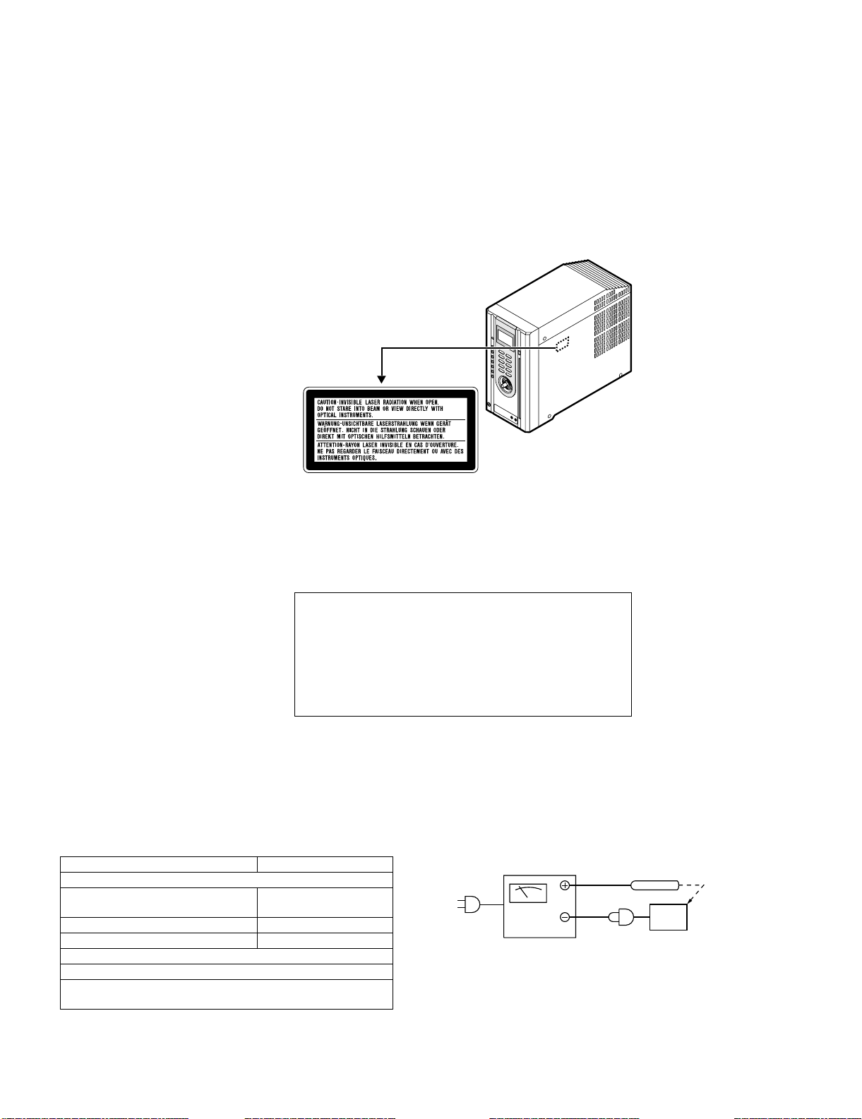
[2] SAFETY PRECAUTION FOR SERVICE MANUAL
Precaution to be taken when replacing and servicing the Laser Pickup.
The AEL (Accessible Emission Level) of Laser Power Output for this model is specified to be lower than Class 1 Requirements. However, the following precautions must be observed during servicing to protect your eyes against exposure to the Laser beam.
1) When the cabinet has been removed, the power is turned on without a compact disc, and the Pickup is on a position outer than the lead-in position, the Laser will light for several seconds to detect a disc. Do not look into the Pickup Lens.
2) The Laser Power Output of the Pickup inside the unit and replacement service parts have already been adjusted prior to shipping.
3) No adjustment to the Laser Power should be attempted when replacing or servicing the Pickup.
4) Under no circumstances look directly into the Pickup Lens at any time.
5) CAUTION - Use of controls or adjustments, or performance of procedures other than those specified herein may result in hazardous radiation
exposure.
Laser Diode Properties
Material: GaAIAs
Wavelength: 780 nm
Emission Duration: continuous
Laser Output: max. 0.6 mW
[3] IMPORTANT SERVICE NOTES (FOR U.K. ONLY)
Before returning the unit to the customer after completion of a repair or
adjustment it is necessary for the following withstand voltage test to be
applied to ensure the unit is safe for the customer to use.
Setting of Withstanding Voltage Tester and set.
Set name set value
Withstanding Voltage Tester
Test voltage 4,240 VPEAK
Set time 6 secs
Set current (Cutoff current) 4 mA
Unit
Judgment
OK: The “GOOD” lamp lights.
NG: The “NG” lamp lights and the buzzer sounds.
ADVARSEL-USYNLIG LASERSTRÅLING VED ÅBNING. SE IKKE IND I
STRÅLEN-HELLER IKKE MED OPTISKE INSTRUMENTER.
VARO! AVATTAESSA OLET ALTTIINA NÄKYMÄTÖN LASERSÄTEILYLLE.
ÄLÄ TUIJOTA SÄTEESEEN ÄLÄKÄ KATSO SITÄ OPTISEN LAITTEEN
LÄPI.
VARNING-OSYNLIG LASERSTRÅLNING NÄR DENNA DEL ÄR ÖPPNAD.
STIRRA EJ IN I STRÅLEN OCH BETRAKTA EJ STRÅLEN GENOM
OPTISKT INSTRUMENT.
VAROITUS! LAITTEEN KÄYTTÄMINEN MUULLA KUIN TÄSSÄ
KÄYTTÖOHJEESSA MAINITULLA TAVALLA SAATTAA
ALTISTAA KÄYTTÄJÄN TURVALLISUUSLUOKAN 1
YLITTÄVÄLLE NÄKYMÄTTÖMÄLLE LASERSÄTEILYLLE.
VARNING - OM APPARATEN ANVÄNDS PÅ ANNAT SÄTT ÄN
I DENNA BRUKSANVISNING SPECIFICERAS. KAN
ANVÄNDAREN UTSÄTTAS FÖR OSYNLIG LASERSTRÅLNING, SOM ÖVERSKRIDER GRÄNSEN FÖR
LASERKLASS 1.
3,000 VRMS
1 – 2
Page 4
XL-DAB9H
FOR A COMPLETE DESCRIPTION OF THE OPERATION OF THIS UNIT, PLEASE REFER TO THE OPERATION MANUAL.
[4] SPECIFICATIONS
Except for U.K.
Genera■
Power source AC 230 V, 50 Hz
Power
consumption
Dimensions Width: 100 mm
Weight 2.3 kg
■
Amplifier
Output power PMPO: 30 W (total)
Output terminals Speakers: 4 ohms
Input terminals Line input: 47 k ohms
■
Tuner
Frequency range DAB: 174 - 240 MHz (Band-III)
For U.K.
Power on: 25 W
Power stand-by: 0.9 W
Height: 205 mm
Depth: 266 mm
MPO: 15 W (7.5 W + 7.5 W) (DIN 45 324)
RMS: 10 W (5 W + 5 W) (DIN 45 324)
Headphones: 16 - 50 ohms
(recommended: 32 ohms)
Line output: 2 k ohms
1,450 - 1,492 MHz (L-Band)
FM: 87.5 - 108.0 MHz
■l
CD player
Type Compact disc player
Signal readout Non-contact, 3-beam semiconductor laser
D/A converter 1-bit D/A converter
Frequency
response
Dynamic range 90 dB (1 kHz)
Speaker
■
Type 2-way type speaker system
Maximum input
power
Rated input power 5W
Impedance 4 ohms
Dimensions Width: 100 mm
Weight 1.2 kg/each
pickup
20 - 20,000 Hz
4 cm tweeter
8cmwoofer
10 W
Height: 205 mm
Depth: 193 mm
Genera
■
Power source AC 230 V, 50 Hz
Power
consumption
Dimensions Width: 100 mm
Weight 2.3 kg
■
Amplifier
Output power RMS: 10 W (5 W + 5 W) (10 % T.H.D.)
Output terminals Speakers: 4 ohms
Input terminals Line input: 47 k ohms
■
Tuner
Frequency range DAB: 174 - 240 MHz
Specifications for this model are subject to change without prior
notice.
l
Power on: 25 W
Power stand-by: 0.9 W
Height: 205 mm
Depth: 266 mm
Headphones: 16 - 50 ohms
(recommended: 32 ohms)
Line output: 2 k ohms
FM: 87.5 - 108.0 MHz
■
CD player
Type Compact disc player
Signal readout Non-contact, 3-beam semiconductor laser
D/A converter 1-bit D/A converter
Frequency
response
Dynamic range 90 dB (1 kHz)
Speaker
■
Type 2-way type speaker system
Maximum input
power
Rated input power 5W
Impedance 4 ohms
Dimensions Width: 100 mm
Weight 1.2 kg/each
pickup
20 - 20,000 Hz
4 cm tweeter
8 cm woofer
10 W
Height: 205 mm
Depth: 193 mm
1 – 3
Page 5
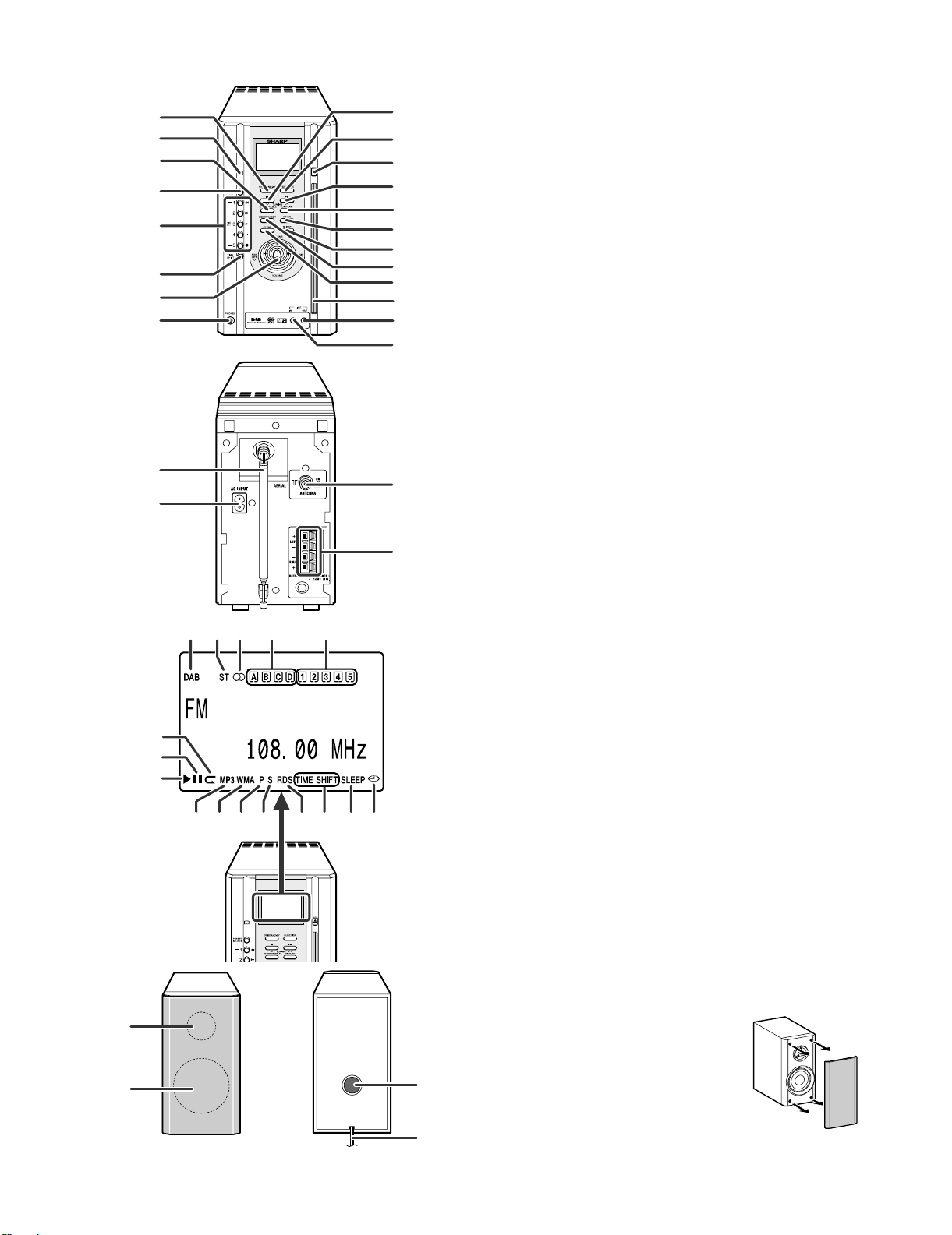
[5] NAMES OF PARTS
1
2
3
4
5
6
7
8
21
22
9
10
11
12
13
14
15
16
17
18
19
20
23
XL-DAB9H
1. On/Stand-by Button
2. Remote Sensor
3. Bass/T reble Selector Button
4. Preset Zone Select Button
5. Preset Number Select/Time Shift Mode Buttons
6. Time Shift Button
7. Volume Up and Down/Track Up and Down/
Preset Up and Down Lever
8. Headphone Socket
9. Disc Stop/Tuning Down Button
10. Function Selector Button
11. D isc Eject Button
12. Disc Play or Pause/Tuning Up Button
13. MP3/WMA Display Button
14. Timer Button
15. S leep Button
16. Memory/Set Button
17. Clear Button
18. Disc Slot
19. Li ne Output Socket
20. Line Input Socket
21. DAB Rod Aerial
22. AC Power Input Socket
23. FM 75 Ohm Aerial Socket
24. S peaker Terminals
24
4
321 5
6
7
8
11 12 13
14 15 16109
1. DAB Indicator
2. FM Stereo Mode Indicator
3. FM Stereo Receiving Indicator
4. Preset Zone Indicators
5. Preset Number Indicators
6. Repeat Play Indicator
7. Pause Indicator
8. Play Indicator
9. MP3 Track Indicator
10. WMA Track Indicator
11. Primary with Secondary Indicator
12. Secondary Indicator
13. RDS Indicator
14. Time Shift Indicator
15. Sleep Indicator
16. Timer Play Indicator
17. Tweeter
18. Woofer
19. Bass Reflex Duct
20. Speaker Wire
Note:
There is no distinction between the right and the left speakers.
17
18
19
20
Speaker grilles are removable:
Make sure nothing comes into contact with the
speaker diaphragm when you remove the
speaker grilles.
1 – 4
Page 6
XL-DAB9H
13 18
14
15
16
32 33
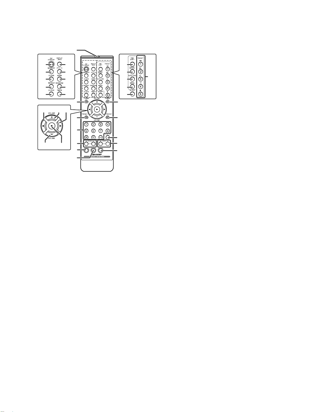
1. Remote Control Transmitter
2. Fast Reverse/Tuning Down Button
3. Track Down/Preset Down Button
4. Direct Search Buttons
1
23
19
20
21
2217
2
31
3029
3
8
9
24
25
26
27
28
4
10
5
6
11
12
7
5. Treble Up and Down Buttons
6. CD Select Button
7. Tuner and Band Selector Button
8. Fast Forward/Tuning Up Button
9. Track Up/Preset Up Button
10. MP3/WMA Display Button
11. Bass Up and Down Buttons
12. Auxiliary Button
13. On/Stand-by Button
14. Memory Button
15. Clear Button
16. Repeat Button
17. Clock Button
18. RDS Display Mode/Information Select Button
19. RDS Programme Type/
Traffic Information Search Button
20. RDS ASPM (Auto Station Programme Memory) Button
21. Random Button
22. Timer Button
23. Time Shift Button
24. Preset Zone Select Button
25. Auto Tune Button
26. M enu Button
27. S leep Button
28. Preset Number Select/Time Shift Mode Buttons
29. Disc Stop Button
30. Volume Up Button
31. D isc Pause Button
32. Volume Down Button
33. Disc Play Button
1 – 5
Page 7
XL-DAB9H
CHAPTER 2. ADJUSTMENTS
[1] ADJUSTMENT
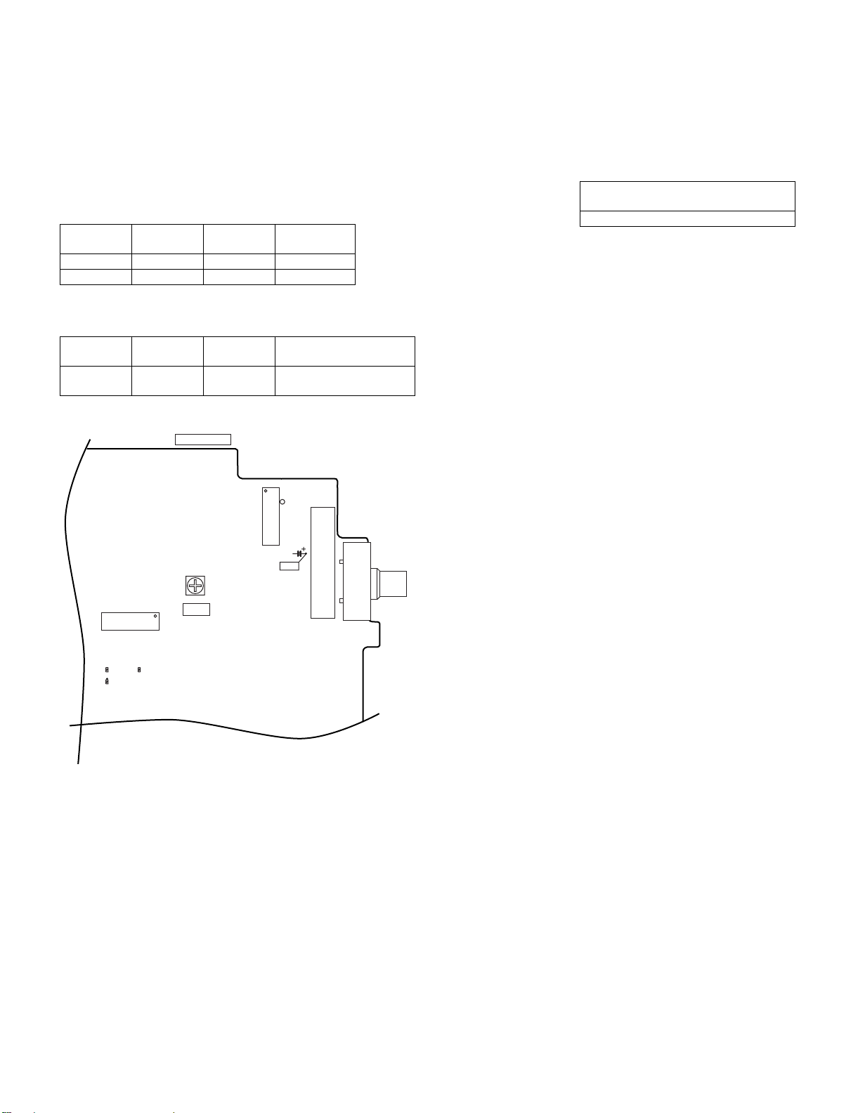
1. TUNER SECTION
fL: Low-range frequency
fH: High-range frequency
• Check FM VT
Signal generator: 1 kHz, 40 kHz dev., FM modulated
Frequency Display Check
Point
87.5 MHz 87.5 MHz 2.2V ± 1.0V TP301
108 MHz 108 MHz 7.3V ± 1.0V TP301
• FM Mute Level
Signal generator: 1 kHz, 40 kHz dev., FM modulated
Frequency Display Adjusting
Parts
98.00 MHz
98.00 MHz VR351*1 Input: SO301
(30 dBµV)
*1.Adjiust so that an output signal appears.
Instrument
Connection
Instrument
Connection
Output: Speaker Terminal
XL-DAB9H
[2] How to check the version number of the
Service Manual
system microcomputer
1. Turn the power off.
2. With holding down “PRESET SELECT” and “PRESET 2” buttons,
turn the power on.
3. The version number displays as below.
Version number display
Ver.08 C ← Version number of the system microcom-
puter
SHP_SER_V1.7.2 ← Version number of DAB module
R356
MAIN PWB-A1
VR351
FM MUTE
IC303
R357
LEVEL
R350
Figure 1 ADJUSTMENT POINTS
IC302
20
C393
TP301
SO301
FE301
2 – 1
Page 8
XL-DAB9H
A
A
[3] TEST MODE
1. Turning on the test mode
Turning on the test mode
To turn on the specific test mode, holding down the following two buttons in the ordinary stand-by mode (power off state). In this case only the main
unit button is valid. Even when the ON/STAND-BY of remote control button is set to on, the test mode is not turned on. Then press the ON/STANDBY button.
[Ordinary test mode]
TEST CONTENTS KEY1 KEY2 KEY3
Tuner and DAB clear test (Test 1) MEMORY PRESET UP ON/STAND-BY
Tuner and DAB test mode (Test 2) FUNCTION BASS/TREBLE ON/STAND-BY
DISPLAY+KEY TEST (Test 3) MEMORY PLAY ON/STAND-BY
CD Test Mode (Test 4) MEMORY FUNCTION ON/STAND-BY
Soft rest test (Test 5) FUNCTION CLEAR ON/STAND-BY
Volume Test Mode (Test 6) BASS/TREBLE VOLUME DOWN ON/STAND-BY
Time Test Mode (Test 7) BASS/TREBLE TIMER ON/STAND-BY
Main line Test Mode (Test 8) PRESET UP BASS/TREBLE ON/STAND-BY
All test modes can be terminated by turning off the power with ON/STAND-BY key.
• Tuner and DAB clear test (Test 1)
All tuner and DAB preset stations are cleared
• Tuner and DAB clear test (Test 2)
PRESET CH BAND FREQUENCY
1 → PRESET1
2 → PRESET2 108.00MHz
3 → PRESET3 90.00MHz
4 → PRESET4 106.00MHz
5 → PRESET5 98.00MHz
6 → A1
7 → A2 239.200MHz
8 → A3 218.640MHz
9 → A4 234.208MHz
10 → A5 206.352MHz
11 → B1 1452.960MHz
12 → B2 1471.792MHz
13 → B3 1490.624MHz
14 → B4 176.640MHz
15 → B5 237.488MHz
• DISPLAY+KEY TEST (Test 3)
FUNCTION: KEY AND DISPLAY
1. into the mode (Press Memory + Play + ON/STAND-BY) first time
display indictor all turn on.
When the following keys are pressed, they are turn off. "kitchen
timer" icon is always turn on.
When all keys are pressed, 5*7 segment are off
1 TIME SHIFT TIME SHIFT
2 PRESET 1 "1" and THE FRAME
3 PRESET 2 "2" and THE FRAME
4 PRESET 3 "3" and THE FRAME
5 PRESET 4 "4" and THE FRAME
6 PRESET 5 "5" and THE FRAME
7 PRESET
SELECT
8 FUNC RDS
9 PLAY "A" and THE FRAME
10 DISP STEREO, STEREO IND
11 F.SKIP PLAY
12 VOL DOWN "D" and THE FRAME
13 STOP "B" and THE FRAME
14 SOUND FM
FM MONO
DAB
KEY OFF
"P", "S"
ICON
87.50MHz
174.928MHz
15 MEMO DAB
16 CLEAR REPEAT
17 B.SKIP PAUSE ICON
18 VOL UP "C" and THE FRAME
19 EJECT MP3 and WMA
20 TIMER TIMER
21 SLEEP SLEEP
• CD Test Mode (TEST 4)
[cd step 1] Enter test mode. ←–––––––
↓ Hold down the “memory” button
[cd step 2]
↓ Hold down the “memory” button
[cd step 3]
↓ Hold down the “memory” button
[cd step 4]
↓ Hold down the “memory” button
[cd step 5] CD playback starts.
↓Hold down the “stop” button to returnto [cd step 1]—→
In step 5, hold down the AUX key on the remote control. The tracking servo is switched on/off.
From step 3, the pick up can be moved with the FF/REW key.
• Soft reset Test (TEST 5)
All data in RAM is cleared.
• Volume Test Mode (TEST 6)
Starting from level 23 (default), check all the levels (0 - 23 - MAX).
• Time Test Mode (TEST 7)
At 1:05, the power turns on to activate the tape function, and turns
off after 90 seconds (equivalent to 90 minutes on the unit).
KEY OFF
After some steps, the laser turns
on.
After some steps, focus search is
performed.
After some steps, CLV rotation is
performed.
2 – 2
Page 9
• Main line Test Mode (TEST 8)
Function: 1. check communication from main micon to DAB unit when without DAB unit.
2. Check volume IC (75341) DAB channel condition.
3. supply condition check
Note: At test mode 8, there is not DAB unit.
TEST8
GO TO POWER OFF MODE.
WHILST HOLDING DOWN THE "PRESET UP" and "BASS/TREBLE" BUTTON, PRESS THE
POWER BUTTON.
(chataring: 10ms x 3)
1 .DISPLAY "Communicate" FOR 1 SECOND
2. Set Volume IC (75341) to DAB channel
3. Set mute off but when volume change to 0 set mute on
XL-DAB9H
Push "preset select" key and change "SCP_CLK" & "SI_DIN" & "SI_DOUT" as follows: (need
display statue on LCD, first line display "CLK DIN DOUT", second line display Pin status.)
CLK DIN DOUT
0
1
0
0
1
0
0
1
0
1
0
0
0
1
1
Push "power" key to enter into standby mode
2 – 3
Page 10
XL-DAB9H
Home StereoXL-DAB9HService ManualXL-DAB9H S/MMarketE
CHAPTER 3. MECHANICAL DESCRIPTION
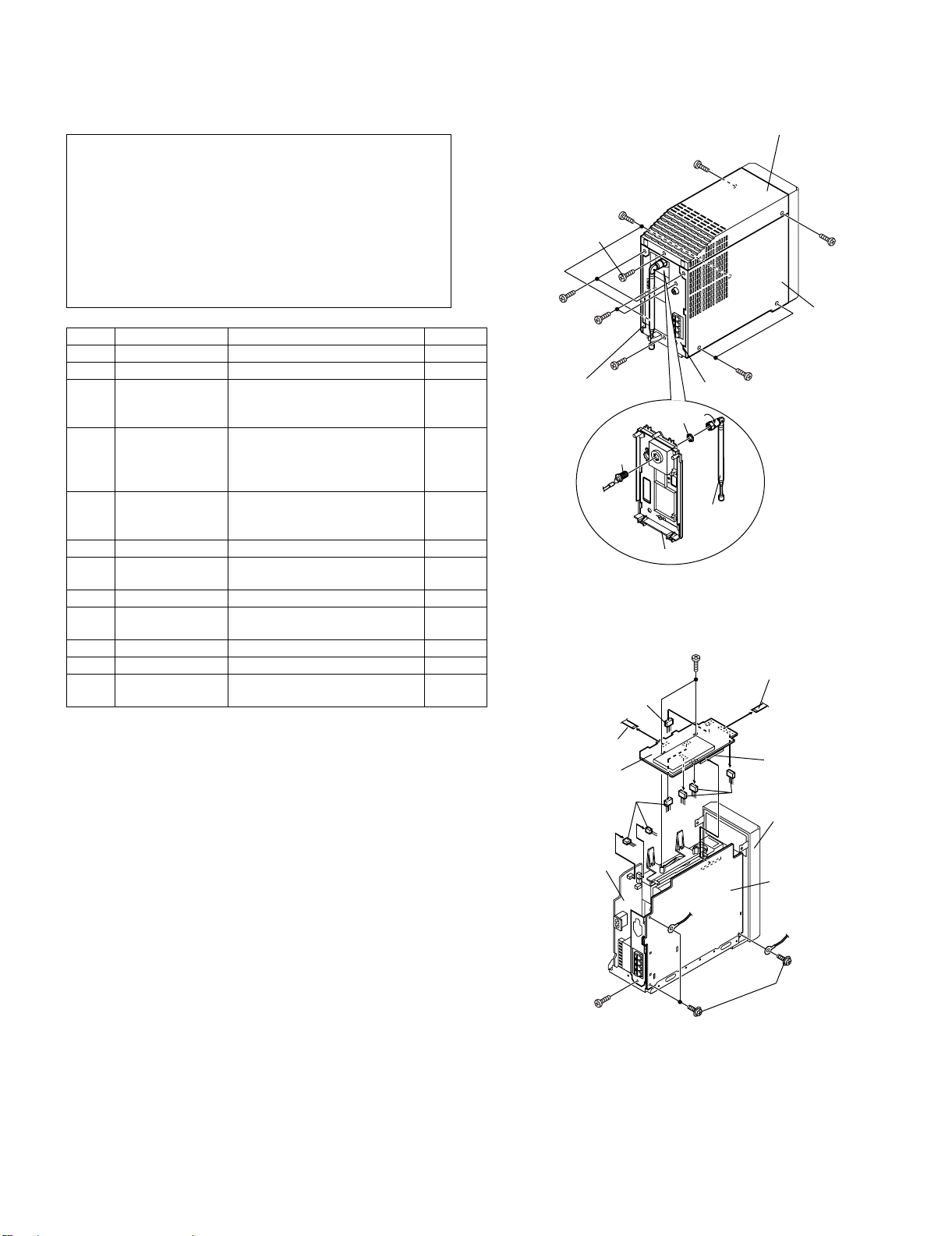
[1] DISASSEMBLY
Caution on Disassembly
Follow the below-mentioned notes when disassembling the unit and
reassembling it, to keep it safe and ensure excellent performance:
1) Be sure to remove the power supply plug from the wall outlet
before starting to disassemble the unit.
2) Take off nylon bands or wire holders where they need to be
removed when disassembling the unit. After servicing the unit,
be sure to rearrange the leads where they were before disassembling.
3) Take sufficient care on static electricity of integrated circuits and
other circuits when servicing.
STEP REMOVAL PROCEDURE FIGURE
1 Top Cabinet 1. Screw...........................(A1) x 5 1
2 Side Panel 1. Screw...........................(B1) x 4 1
3 Rear Panel 1. Screw..........................(C1) x 3
2. Antenna.......................(C2) x 1
3. Nat..............................(C3) x 1
4 Display PWB 1. Screw..........................(D1) x 2
2. Flat cable.....................(D2) x 2
3. Socket.........................(D3) x 7
4. Socket.........................(D4) x 1
5 Main PWB 1. Screw..........................(E1) x 4
2. Socket.........................(E2) x 6
3. Flat cable.....................(E3) x 1
6 Front Panel 1. Screw...........................(F1) x 1 3
7 CD Mechanism
1. Screw..........................(G1) x 4 4
Unit
8 Power PWB 1. Screw..........................(H1) x 4 4
9 Sensor PWB 1. Screw..........................(J1) x 4
2. Socket.........................(J2) x 2
10 Switch PWB 1. Screw..........................(K1) x 7 5
11 Jack PWB 1. Screw...........................(L1) x 2 5
12 CD Mechanism
(Note)
1. Screw..........................(M1) x 4
2. Spring..........................(M2) x 1
1
2
2
3
3
5
6
(A1)x1
ø3x12mm
(A1)x2
ø3x12mm
(C1)x2
ø3x12mm
Side Panel
(Right)
(B1)x2
ø3x6mm
(C1)x1
ø3x8mm
Antenna
terminal
(A1)x1
Top Cabinet
ø3x12mm
(A1)x1
ø3x12mm
Side Panel
(Lift)
(B1)x2
ø3x6mm
Rear Panel
(C3)x1
(C2)x1
Rear Panel
Figure 1
(D1)x2
ø3x10mm
(D2)x1
(D3)x1
Note:
After removing the connector for the optical pickup from the connector,
wrap the conductive aluminium foil around the front end of the connector so as to protect the optical pickup from electrostatic damage.
(D2)x1
Display PWB
Power PWB
(E1)x1
ø3x6mm
(D3)x3
(D4)x1
(D3)x3
Front Panel
Main PWB
(E1)x3
ø3x12mm
Figure 2
3 – 1
Page 11
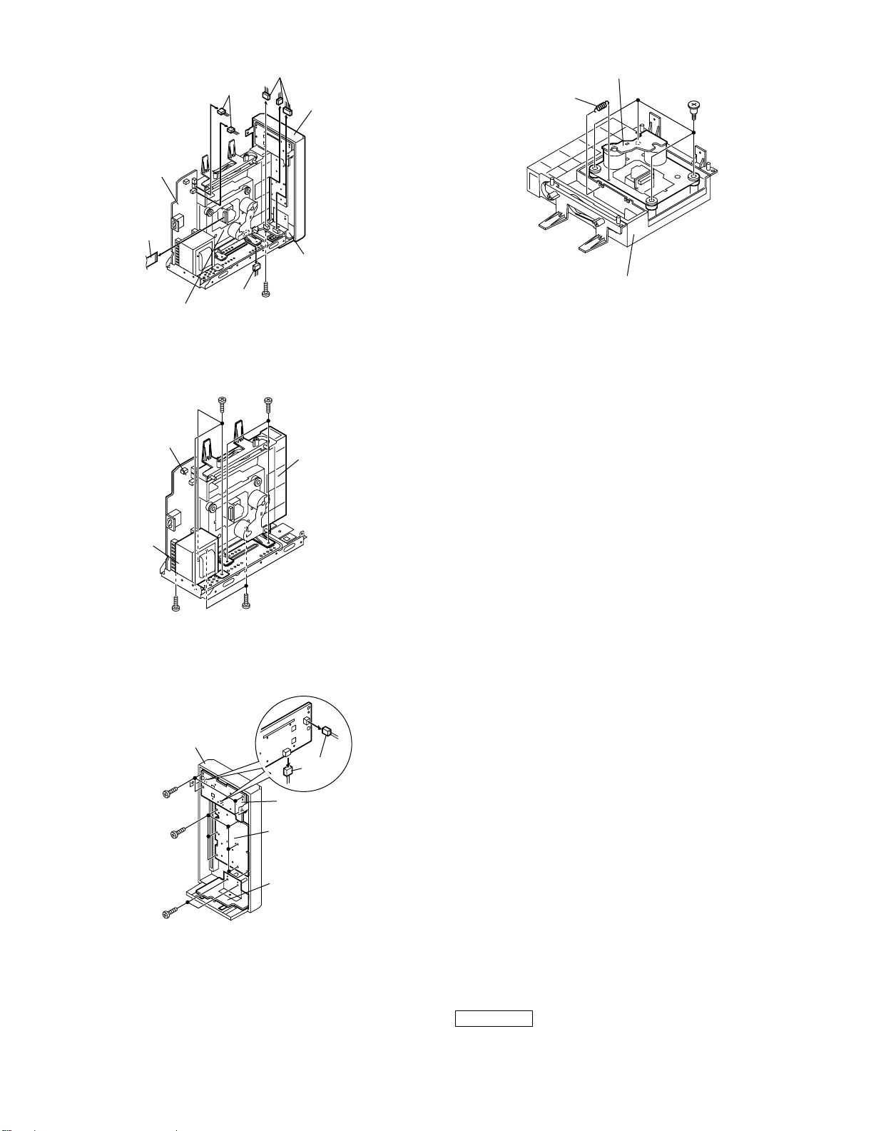
XL-DAB9H
Power PWB
(E3)x1
CD Mechanism
Power PWB
(E2)x2
Figure 3
(H1)x3
ø3x6mm
(E2)x1
(E2)x3
(F1)x1
ø3x6mm
(G1)x2
ø3x6mm
Front Panel
Jack PWB
CD
Mechanism Unit
(M2)x1
CD Mechanism
CD
Mechanism Unit
Figure 6
(M1)x4
ø2.5x12mm
Transformer
(J1)x4
ø2.5x10mm
(K1)x7
ø2.5x10mm
(L1)x2
ø2.5x10mm
(G1)x2
ø3x8mm
(H1)x1
ø3x6mm
Figure 4
Front Panel
(J2)x2
Sensor PWB
Switch PWB
Jack PWB
Figure 5
CP-DAB9H
These speaker CP-DAB9H are available in assembles only and may
not be disassembled.
3 – 2
Page 12
XL-DAB9H
F
B
A
E
FO+
TR+
TR-
FO-
ACTUATOR
TR+
FO+
FO-
C
F
B
A
E
TR-
C
D
VCC
VC
LD
VR
MD
D
GND
LD
VR
MD
F
B
A
E
FO+
TR+
TR-
FO-
C
D
VCC
VC
GND
LD
VR
MD
8
6
5
3
13
14
15
16
7
4
2
1
9
10
11
12
8
6
5
3
13
14
15
16
7
4
2
1
9
10
11
12
CD PICKUP UNIT
CD MECHANISM UNIT
MECHANISM PWB
+
+
-
-
SP+
SPÐ
SL+
SLÐ
PU-IN
GND
PICKUP IN
SLED
MOTOR
SPINDLE
MOTOR
M
M
MP3 DECODER
DIGITAL SIGNAL
PROCESSOR
FOCUS/TRACKING/
SPIN/SLED DRIVER
EFMIN
SLCO
AVDD
RF
LPF
PHLPF
AIN
CIN
BIN
DIN
FEC
RFMON
VREF
JITTC
EIN
FIN
TEC
TE
TEIN
LDD
LDS
VSS
AVDD
FDO
TDO
SLDO
SPDO
VVSS1
PDOUT1
PDOUT0
PCKIST
VVDD1
DMUTEB
PUIN
DEFECT
FSEQ
C2F
DVDD
DVSS
DVDD1.8
VVDD3
TES
STDA
ST
STR
TES
CON
CON
CON
INT
INT
RE
RCHO
LRVSS
LRVDD
LCHO
XVDD
XIN
XOUT
XVSS
AMUTEB
DOUT
DVDD
DVSS
DVDD1.8
VVSS2
VCOC2
VPREF2
VPDOUT2
DV
DV
1
2
3
4
5
6
7
8
9
10
11
12
13
14
15
16
17
18
19
20
21 22 23 24 25 26 27 28 2930 31 32 33 34 35 36 37 38
16 17 18 19 20 21 22 23 2425 26 27 28 29 30
151413121110987654321
39
80 79 78 77 76 75 74 73 7271 70 69 68 67 66 65 64 63 62
LC78690
1
2
3
4
5
6
1
2
3
4
5
6
1
2
3
4
5
6
7
LA6548ND
VINT
VG3
VO3+
VO3-
CD
RESET
REG-IN
VO4-
VO4+
VIN4
VG4
VREF
VIN2
REG-OUT
VO2+
VO2-
VG2
VO1-
VG1
GND
GND
GND
VO1+
GND
GND
GND
GND
VCC
MUTE
VCC
+B
+B
+B
+B
+B
+B
16.93MHz
+B
+B
LASER
DRIVER
CON
VOL
CONSTANT
VOLTAGE
STEREO
SD
CF351
FM IF
24
22
21
20
19
18
17
16
15
14
13
12
11
10
9
8
7
6
5
4321
IC303
LA1832S
22
21
20
17
16
15
14
13
12
12 3 4
5
6
7
8
897106115124133142151
16
9
10
11
IC302
LC72131
IC521
LC72723M
X352
X351
456kHz
L354
LOW PASS
FILTER
XIN
NC
CEDICL
MO/ST
FM
FM
DO
CEDICL
DO
FM IN
XOUT
DATA
CLE
VSS
AOUT
VDD
AM IN
NC
IF IN
IF REQ
SW
VCC
VR351
10K(B)
FM MUTE LEVEL
23
+5V
MUTE
R-MUTE
MO/ST
L-CH OUT
R-CH OUT
MPX VCO
AM LOW CUT
FM/AM OUT
MPX IN
AM OSC OUT
FM AFC
AM RF IN
VSM
AM OSC INAM MIX OUT
AM IF IN
GND
REG
FM IF IN
SD
STEREO
FM DET
PHASE
(AM/FM)
IF OUT
PHASE
FM IF DET./FM MPX./AM IF
FE301
FM FRONT END
4.5MHz
Q351
SWITCHING
R_MUTE
PLL TUNER
RDS
ZD351
Q360
FM+B
TUN+B
TUN+B
FM+B
FM RF
AM OSC OUT
A_GND
+5V
D_GND
CF302
1
2
3
21345678
10.7MHz
FM IF
CF301
1
2
3
10.7MHz
VT
FM
SO301
FM
ANTENNA
TERMINAL
Q301
Q521
FC801
Q802
X801
Q805
IC802
IC801
Q801
Q809
Q808
Q810
+B1
+B1
Q806
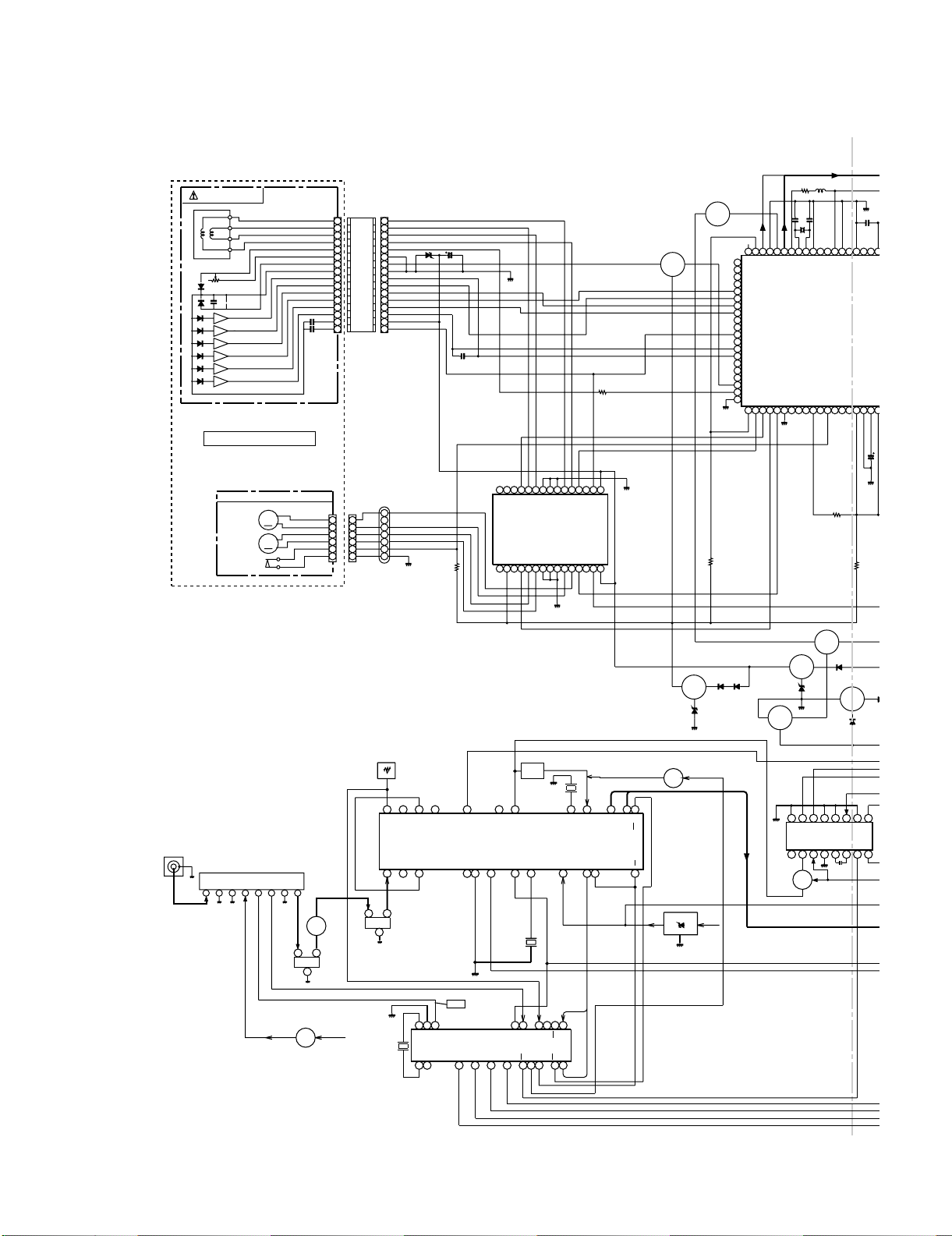
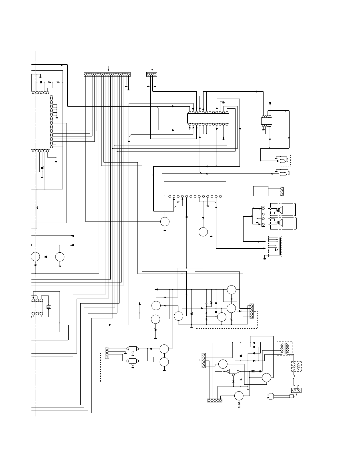
CHAPTER 4. DIAGRAMS
[1] BLOCK DIAGRAM MAIN
Figure 4-1 BLOCK DIAGRAM (1/4)
4 – 1
Page 13
XL-DAB9H
FSEQ
DVSS
7666564636261
VVSS2
VCOC2
DVDD1.8
TEST1
VPDOUT2
STDATA
STCK
STREQ
TEST0
CONT0
CONT1
CONT2
R
INTB1
AL
INTB0
RESB
R
DVSS
DVDD
C2F
DVDD
DVSS
4353637383940
VVDD3
DVDD1.8
+B
+B
CONSTANT
VOLTAGE
Q808
VVDD2
VPREF2
DO
DI
CL
CE
VVSS3
60
59
58
57
56
55
54
53
52
51
50
49
48
47
46
45
44
43
42
41
CD_L
CD_R
LRSY
DATACK
DATA
Q803
+B
+12V
CD-VCC
O_CD_RESET
I_CD_DATA
O_CD_DATA
O_CD_CLK
O_CD_CE
+B1
+B1
FROM DISPLAY FROM DISPLAY
24 8675913 2413
O_CD_CLK
O_P_MUTE
I_CD_DATA
O_CD+B
O_CD_CE
O_CD_DATA
O_CD_RESET
FM ST
O_POWER
0_AMP_ON
11 13 1715 1614 18 19 2010 12
SD
VSM
O_TU_CE
I_TU_SDI
O_TU_SCK
O_TU_SDO
D_GND
RDS_CLK
RDS_DATA
+B2
M+5V
CNP501 CNS502
D_GND
DAB_R
D_GND
DAB_L
CD L
LC75341M
AUDIO
PROCESSOR
CD R
R.F
(L)
Q107
Q108
MUTING
IC601
IN1
TUN L
TUN R
PRE.GND
(R)
IN2
STBY
4321
5
AUX L
101112
L4L3L2
L1
LSL0
R3R1R2CLR4
RSL0
151413 181716 212019 242322
AUX R
P.P
VCC
OUT2
8
9
6
7
(R)
Q104
LIN
RIN
P_GND
10
LTRE
RTRE
11
LBS
RBS
12
LOUT
R OUT
OUT1
(L)
LOUT
ROUT
CL
CE
DI
13
VSS
VREF
+B1
(L)
(R)
123456789
DI
CE
VDD
IC101
LA4631++
POWER AMP.
Q651~653
J101
SPEAKER
TERMINAL
+B1
LOUT
678
15234
R OUT
R OUT
LOUT
LIN
RIN
5V
SPEAKER BOX A'SSY
1
2
3
4
SPEAKER BOX A'SSY
IC602
PRE.AMP.
NJM14558
1
2
3
1
2
3
3
2
1
CNS730
L-CH
J103
HEADPHONES
SO601
LINE OUT
SO201
LINE IN
TO DISPLAY
R-CH
CD+B
VSM
RDS_DATA
RDS_CLK
SD
11
X521
456 kHz
897106
+5V
FM ST
DO
CL
DI
CE
TUN_L
TUN_R
CONSTANT VOLTAGE
DAB_+3.3V
1
DAB_GND
2
DAB_+5V
3
DAB_POWER
4
CNS510
CONSTANT VOLTAGE
IC141
BAD33T++
REGULATOR
3
2
3
2
IC140
KIA7805API
REGULATOR
+B2
M+5V
1
1
TO DISPLAY
12V
+B1
Q105
Q109
Q150
Q151
P-ON
Q106
+B
D113
1
2
3
4
5
ZD111
GND
VP
LED+11.3V
VP
21
TO DISPLAY
D110
Q103
Q110
KIA7805API
CONSTANT
VOLTAGE
REGULATOR
+5.6V
3
45
Q101
Q102
3
IC151
TO CHASSIS GND
CNP102
1
2
3
4
5
D101
D102
D103
D104
RP602
1
2
Q154
Q128
PT1
POWER TRANSFORMER
L101
LINE
FILTER
F101
T200mA L250V
SO102
AC INPUT
SOCKET
AC POWER
SUPPLY CODE
AC 230V 50Hz
Figure 4-2 BLOCK DIAGRAM (2/4)
4 – 2
Page 14
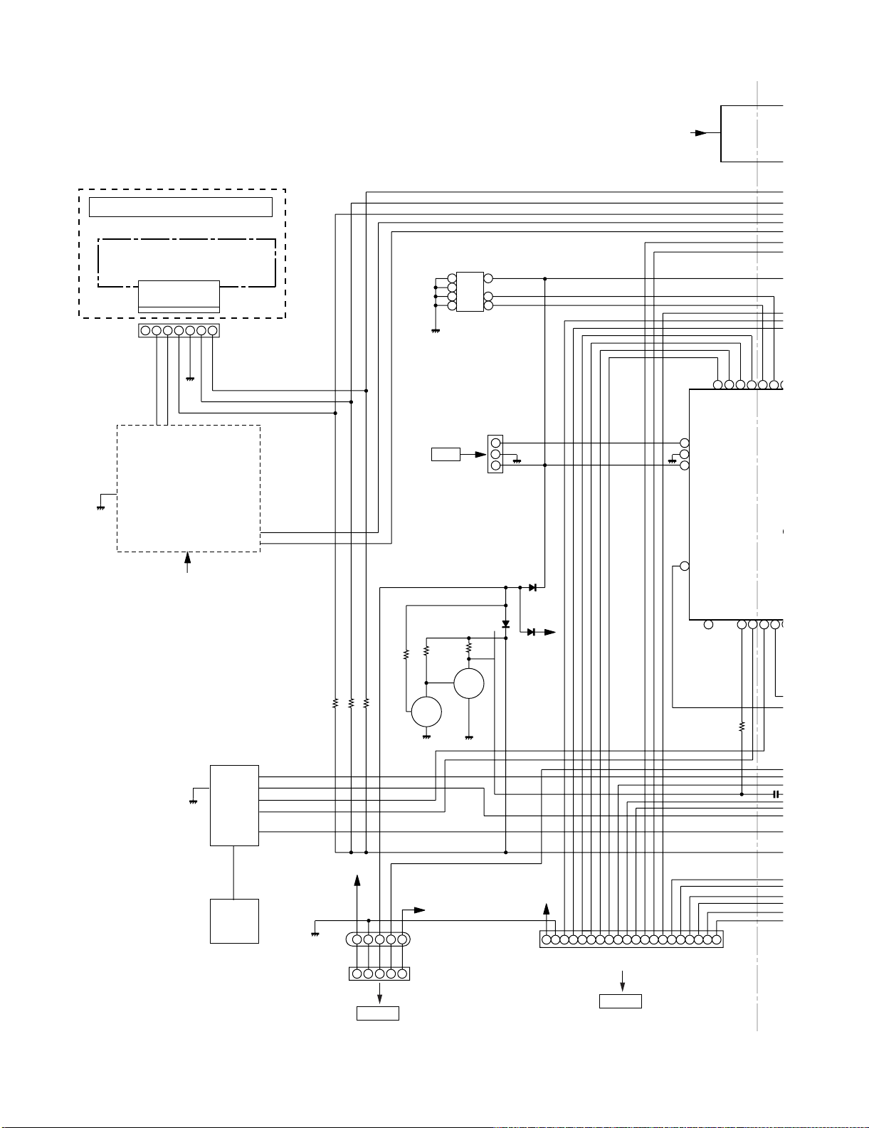
XL-DAB9H
5
O
O
C
[2] BLOCK DIAGRAM DISPLAY
SLOT IN MECHANISM A'SSY
MECHANISM PWB
1324657
CNP701
SW1
SW3
SW2
MM-
MM+
M_GND
Q701~Q706
DISC SLOT-IN
M_GND
MECHA DRIVER
MM+
MM-
SW1
SW2
SW3
IC7A1
AT24C04
EEPROM
1
2
3
4
EEP-GNDD
FROM JACK PWB
CNS730
EEP-VDDD
8
6
5
CNP730
3
2
1
EEP-CLK
EEP-DATA
ROD ANTENNA
+B
TU_CE
69
LINE_OUT_MUTE
GND
+B
70
VDD3
71
TU_DI
TU_CLK
TUN
AMP_
TU_DO
O_P
565758596061
EEP_CLK
EEP_DATA
MI
+B2
D_GND
KEY
SW701~706
SW707
SW709~715
SW716~722
OPEN_CLOSE
KEY
SW708
I_KEY3
DAB_KEY
I_KEY1
I_KEY2
I_POWER
D_GND
+B
+B5
NEC_+4V
+5.6V
CNP102
TO POWER
VP
LED+11V
CNW102
134
1235645
CNS102
Q707
80
D704
+B
D705
D703
+B4
LED_CON
PROG_ENA
HOLD
KEY3
36789
POWER
REM
Q709
D_GND
CNW501
+B2
M+5V
D_GND
RDS_CLK
I_TU_SDI
RDS_DATA
O_TU_SDO
VSM
O_TU_CE
O_TU_SCK
SD
1011121314151617181920
FM ST
O_POWER
O_CD+B
0_AMP_ON
O_CD_CE
I_CD_DATA
O_CD_DATA
O_CD_RESET
123456789
O_CD_CLK
O_P_MUTE
+B1
CNP501
TO MAIN
Figure 4-3 BLOCK DIAGRAM (3/4)
4 – 3
Page 15
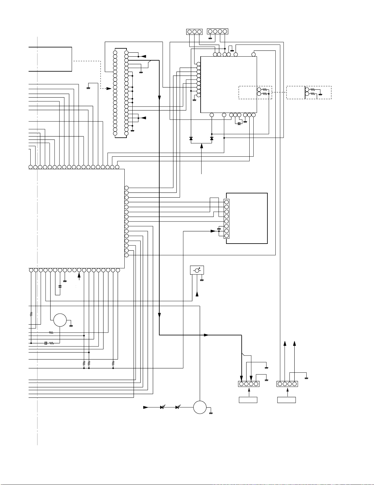
XL-DAB9H
TUN1
O_POWER
AMP_ON
TU_DI
TU_DO
EEP_CLK
EEP_DATA
E
MICROCOMPUTER
HOLD
KEY3
POWER
REM
10 11 12 13 14 15 16 17 18 19 20 21 22 23 24
6789
MM-
RDS_CLK
RDS_DATA
IC701
IXA063SJ
SYSTEM
RES
XT2
XT1
32.768 KHz
X702
MM+
VSS1
D_GND
SW3
CF1
SW2+4
CF2
+B4
SW1
VDD1
CD_ON
KEY1
POWER
AMP_ON
KEY2
RDS_VSM
GND
TU_SD
VDD2
FM_ST
44
43
42
41
40
39
38
37
36
35
34
33
32
31
30
29
28
27
26
25
24
23
CNP701
41424344454647484950515253545556575859
DAB_EN
DAB_ON
DAB_RES
DAB_CLK
DAB_DI
DAB_DO
LCD_RES
LCD_RS
LCD_CLK
LCD_CSB
LCD_DATA
CD_CLK
CD_DI
CD_DO
CD_CE
CD_RES
P_MUTE
SUFIX
VOL_ENC
1
2
3
4
5
6
7
8
9
10
11
12
13
14
15
16
17
18
19
20
21
22
40
39
38
37
36
35
34
33
32
31
30
29
28
27
26
DAB_KEY
AAUD_L
AAUD_R
DAB_GND
DAB_AGND
GND
AV_REF
34
VPP
RESET
1516
VSS0
VDD0
IXA066SJ
4321
CNP708B
VDD
VSS0
VDD0
DAB_POWER(0)
IC702
MODE_SEL
SDRAM_SEL
RESET
36 39 40 41 42 43 44
8
7
6
5
4
3
2
1
RST
RS
CSB
SCL
SI
VSS
VDD
VOU
X703
8MHz
VSS1
X1X2IC(VPP)
LCD701
FL DISPLAY
DAB_MUTE_OUT
17910
56
55
PON_DET
DAB_EN
(FOR U.K.)
MODE_SEL
SDRAM_SEL
DAB_GND
56
55
CNP708A
+B7
+B6
I_REM
LED_CON
SO3
SCK3
17
18
19
20
21
22
23
24
25
RX701
REMOTE
SENSOR
123
+5V
+B3
321
SI3
SCK3
SI
SO
SCK
SI_DIN
SI_DOUT
SCP_CLK
VDDI
AVSS
+B5
Q710
+12V
+B1
LED701
LED702
Q708
Figure 4-4 BLOCK DIAGRAM (4/4)
4 – 4
DAB_L
DAB_R
CNS502
FROM MAIN
DAB_AGND
M_GND
1234
+B7
+B6
DAB_+3.3V
DAB_+5V
DAB_POWER
1234
CNP510CNP502
CNS510
FROM POWER
DAB_GND
Page 16
XL-DAB9H
Home StereoXL-DAB9HService ManualXL-DAB9H S/MMarketE
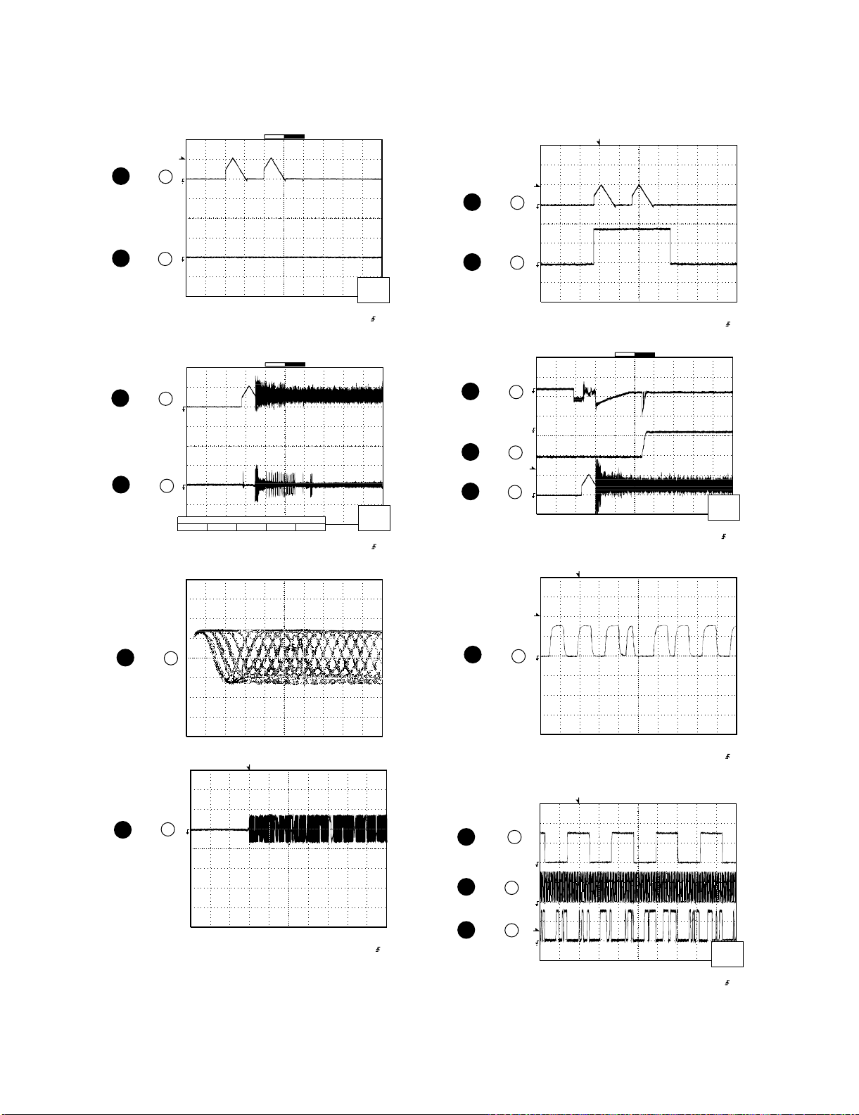
CHAPTER 5. CIRCUIT DESCRIPTION
[1] WAVEFORMS OF CD CIRCUIT
IC801 22
1
IC801 23
2
IC801 22
1
3
IC801 16
Stopped
CH1=500 mV
DC 10:1
T
FDO
1
TDO
3
Smoothing : ON CH1 : 0.000V
BW : FULL
1
3
Smoothing : ON CH1 : 0.000 V
BW : FULL
CH2 : 0.0 V
CH3 : 0.000 V
CH4 : 0.00V
Stopped
CH1=500 mV
DC 10:1
FDO
TE
-3 div -1 div 0 div +1 div +3 div
CH2 : 0.0 V
CH3 : 0.00V
CH4 : 0.00V
CH2=10 V
DC 10:1
CH Position To
CH3=500 mV
DC 10:1
=Record Length=
Main : 100 K
Zoom : 2 K
CH3=1 V
DC 10:1
=Record Length=
Main : 100 K
Zoom : 2 K
500 ms/div
(500 ms/div)
NORM:20 kS/s
CH1
v/DIV
500 mV
=Trigger==Filter= =Offset=
Mode : AUTO
Type : EDGE CH1
Delay : 0.0 ns
Hold off : 0.2 µs
500 ms/div
(500 ms/div)
NORM:20 kS/s
CH2
Position
0.20 div
=Trigger==Filter= =Offset=
Mode : AUTO
Type : EDGE CH1
Delay : 0.0 ns
Hold off : 0.2 µs
1
5
6
7
1
IC801 22
IC801 2 5
IC801 28
IC801 27
IC801 22
Stopped
CH1=200 mV
DC 10:1
T
FDO
2
SPDO
1
Smoothing : ON CH1 : 0.000 V
BW : FULL
Stopped
CH1=500 mV
DC 10:1
PDOUT0
3
4
PDOUT1
T
FDO
1
Smoothing : ON CH1 : 0.000 V
BW : FULL
Stopped
CH1=2 V
DC 10:1
T
T
CH2=500 mV
DC 10:1
CH2 : 0.000 V
CH3 : 0.00V
CH4 : 0.00V
CH2 : 0.0 V
CH3 : 0.00V
CH4 : 0.00V
T
=Record Length=
Main : 100 K
Zoom : 2 K
CH3=1 V
DC 10:1
=Record Length=
Main : 100 K
Zoom : 2 K
1999/04/07 09:51:15
(500 ms/div)
NORM:20 kS/s
=Trigger==Filter= =Offset=
Mode : NORMAL
Type : EDGE CH2
Delay : 2.924 ms
Hold off : 0.2 µs
1999/04/05 17:33:17
CH4=1 V
500 ms/div
(500 ms/div)
DC 10:1
NORM:20 kS/s
=Trigger==Filter= =Offset=
Mode : AUTO
Type : EDGE CH2
Delay : 0.0 ns
Hold off : 0.2 µs
1999/04/07 09:25:28
(500 ns/div)
NORM:200 MS/s
500 ms/div
CH1
v/DIV
500 mV
500 ns/div
4
3
IC801 2
IC801 16
RF
Stopped
CH1=10 V
DC 10:1
TE
2
=Filter= =Offset=
Smoothing : ON CH1 : 0.0 V
BW : FULL
T
CH2=1 V
DC 10:1
CH2 : 0.00 V
CH3 : 0.00 V
CH4 : 0.00 V
=Record Length=
Main : 100 K
Zoom : 2 K
Vp-p=1.0 V~1.3 V
0.5 mV/div,0.5 µsec/div
100 ms/div
(100 ms/div)
NORM:100 kS/s
=Trigger=
Mode : NORMAL
Type : EDGE CH1
Delay : 2.924 ms
Hold off : 0.2 µs
8
9
10
11
IC801 69
IC801 60
IC801 59
IC801 58
1
DOUT
Smoothing : ON CH1 : 0.00 V
BW : FULL
1
2
T
3
Smoothing : ON CH1 : 0.00 V
BW : FULL
Stopped
LRSY
DATACK
DATA
CH1=2 V
DC 10:1
CH2 : 0.00V
CH3 : 0.00V
CH4 : 0.00V
T
CH2=2 V
DC 10:1
CH2 : 0.00V
CH3 : 0.00V
CH4 : 0.00V
=Record Length=
Main : 1 K
Zoom : 100
CH3=2 V
DC 10:1
=Record Length=
Main : 5K
Zoom : 100
=Trigger==Filter= =Offset=
Mode : NORMAL
Type : EDGE CH1
Delay : 2.887 ms
Hold off : 0.2 µs
1999/04/05 20:50:17
5 µs/div
(5 µs/div)
NORM:100 kS/s
CH3
v/DIV
=Trigger==Filter= =Offset=
Mode : AUTO
Type : EDGE CH3
Delay : 0.0 ns
Hold off : 0.2 µs
2V
5 – 1
Page 17
[2] VOLTAGE
XL-DAB9H
PIN
NO.
10
11
12
13
PIN
NO.
PIN
NO.
PIN
NO.
PIN
NO.
10
11
12
13
14
15
16
17
18
19
20
21
22
PIN
NO.
10
11
12
13
14
15
16
17
18
19
20
21
22
23
24
1
2
3
4
5
6
7
8
9
1
2
3
1
2
3
1
2
3
1
2
3
4
5
6
7
8
9
1
2
3
4
5
6
7
8
9
IC101
VOLTAGE
9.14V
1.62V
0V
1.62V
1.51V
12V
18.3V
9.21V
0V
0V
0V
9.15V
0V
IC140
VOLTAGE
11.6V
0V
5V
IC141
VOLTAGE
11.6V
0V
3.3V
IC151
VOLTAGE
16.5V
0.6V
5.6V
IC302
VOLTAGE
2.4 V
0V
0V
0V
0V
5V
0.17 V
0.1 V
3.7 V
0V
0V
0V
0V
0.1 V
0V
2.4 V
4.9 V
0.9 V
0.9 V
2.2 V
0V
2.4 V
IC303
VOLTAGE
2V
4.2 V
2V
2V
0V
4.9 V
4.9 V
2.6 V
4.8 V
0V
3.7 V
3.7 V
2V
1.2 V
1.2 V
2V
4.9 V
2.2 V
0.3 V
0.3 V
0.4 V
2.4 V
4.8 V
3.3 V
PIN
NO.
10
11
12
13
14
15
16
PIN
NO.
10
11
12
13
14
15
16
17
18
19
20
21
22
23
24
PIN
NO.
PIN
NO.
10
11
12
13
14
15
16
17
18
19
20
21
22
23
24
25
26
27
28
29
30
1
2
3
4
5
6
7
8
9
1
2
3
4
5
6
7
8
9
1
2
3
4
5
6
7
8
1
2
3
4
5
6
7
8
9
IC521
VOLTAGE
2.5V
2.5V
5.1V
0V
5V
2.3V
0.6V
2.5V
2.5V
0V
5.1V
0V
0V
1.3V
1.3V
0V
IC601
VOLTAGE
3.5 V
3.5 V
0V
3.5 V
3.5 V
3.5 V
3.5 V
3.5 V
3.5 V
3.5 V
3.5 V
3.5 V
3.5 V
3.5 V
3.5 V
3.5 V
3.5 V
3.5 V
3.5 V
3.5 V
3.5 V
3.5 V
7V
3.5 V
IC602
VOLTAGE
6V
6V
6V
6V
6V
6V
6V
12 V
IC802
VOLTAGE
7.75V
2.77V
1.45V
1.47V
3.9V
3.3V
0V
0V
0V
3.5V
3.7V
1.46V
1.45V
2.9V
1V
2.9V
3.4V
1.45V
1.45V
3.7V
3.6V
0V
0V
0V
3.6V
3.6V
1.46V
1.46V
1.46V
7.8V
PIN
NO.
10
11
12
13
14
15
16
17
18
19
20
21
22
23
24
25
26
27
28
29
30
31
32
33
34
35
36
37
38
39
40
41
42
43
44
45
46
47
48
49
50
51
52
53
54
55
56
57
58
59
60
61
62
63
64
65
66
67
68
69
70
71
72
73
74
75
76
77
78
79
80
1
2
3
4
5
6
7
8
9
IC701
VOLTAGE
0V
0V
0V
0V
0V
5V
5V
5V
5V
5V
1.4V
2.5V
0V
4.3V
5.1
V
5.1
V
5V
5V
0V
0V
0V
2V
0.4V
5V
0V
4V
4.4V
0V
0V
0V
2V
0V
0V
5V
5V
0V
5V
0V
0V
3.9V
4.8V
0V
5V
5V
0V
0V
0V
0V
5V
5V
5V
0V
0V
2.4V
2.5V
0V
0V
0V
5V
0V
0V
0V
0V
0V
0V
0V
0V
0V
4.8V
0V
4.9V
0V
0V
0V
0V
0V
0V
0V
0V
3V
PIN
NO.
10
11
12
13
14
15
16
17
18
19
20
21
22
23
24
25
26
27
28
29
30
31
32
33
34
35
36
37
38
39
40
41
42
43
44
45
46
47
48
49
50
51
52
53
54
55
56
57
58
59
60
61
62
63
64
1
2
3
4
5
6
7
8
9
IC702
VOLTAGE
3.6V
0V
0V
0V
0V
0V
3.5V
0V
0V
3.6V
0V
0V
0V
0V
0V
0V
0V
0V
0V
3.6V
0.9V
3.6V
3.6V
3.6V
0V
1.1V
1.1V
1.1V
1.1V
1.1V
1.1V
1.1V
1.2V
4V
0V
3.3V
2.2V
1.6V
0V
4V
0.9V
0V
1.4V
3.2V
1V
0V
0V
0V
0V
0V
0V
0V
4V
4V
4.2V
0V
0V
0V
0V
0V
0V
0V
0V
0V
PIN
NO.
10
11
12
13
14
15
16
17
18
19
20
21
22
23
24
25
26
27
28
29
30
31
32
33
34
35
36
37
38
39
40
41
42
43
44
45
46
47
48
49
50
51
52
53
54
55
56
57
58
59
60
61
62
63
64
65
66
67
68
69
70
71
72
73
74
75
76
77
78
79
80
1
2
3
4
5
6
7
8
9
IC801
VOLTAGE
1.38V
1.47V
1.45V
1.2V
1.6V
1.7V
1.67V
1.63V
1.42V
1.4V
1.46V
1.74V
1.75V
1.74V
1.43V
1.43V
1.43V
2V
0.18V
0V
2.9V
1.47V
1.5V
1.5V
1.6V
0V
0V
1V
0.93V
2.74V
0V
2.8V
0V
2.8V
0V
2.8V
0V
1.8V
2.8V
0V
2.8V
0V
0.45V
3V
3V
0V
3.23V
2.8V
2.8V
2.8V
0V
0V
0V
0V
0V
0V
0V
0V
0V
0V
2.57V
1.44V
2.1V
2.1V
0V
1.8V
0V
2.8V
0V
0V
0V
1V
1.14V
2.7V
1.64V
3.3V
0V
1.64V
2.9V
1.4V
Q104
PIN NO. VOLTAGE
E
0V
C
3V
0.6V
B
Q105
PIN NO. VOLTAGE
E4.7V
C4.7V
B3.9V
Q106
PIN NO. VOLTAGE
E
0V
C
0V
0.7V
B
Q107
PIN NO. VOLTAGE
E
0V
C
0V
0V
B
Q108
PIN NO. VOLTAGE
E
0V
C
0V
0V
B
Q109
PIN NO. VOLTAGE
E
0V
C
12.3V
5.3V
B
Q110
PIN NO. VOLTAGE
E
0V
C
0V
3V
B
Q128
PIN NO. VOLTAGE
E
17.5V
C
17.4V
16.7V
B
Q150
PIN NO. VOLTAGE
E
12V
C
0.9V
12V
B
Q151
PIN NO. VOLTAGE
E
12V
C
12V
0V
B
Q154
PIN NO. VOLTAGE
E
4.5V
C
16.7V
4.9V
B
Q301
PIN NO. VOLTAGE
E
0V
C
9.5V
0.8V
B
Q351
PIN NO. VOLTAGE
E
0V
C
4.7V
3.7V
B
Q360
PIN NO. VOLTAGE
E
12V
C
11V
11V
B
Q521
PIN NO. VOLTAGE
E
2V
C
5.1V
2.5V
B
Q651
PIN NO. VOLTAGE
E
12.3V
C
12.3V
11.5V
B
Q652
PIN NO. VOLTAGE
E
0V
C
0V
3.7V
B
Q653
PIN NO. VOLTAGE
E
0V
C
0V
3.7V
B
Q701
PIN NO. VOLTAGE
E
4.7V
C
1.3V
4.2V
B
Q702
PIN NO. VOLTAGE
E
0V
C
4.3V
10V
B
Q703
PIN NO. VOLTAGE
E
0V
C
4.3V
10V
B
Q704
PIN NO. VOLTAGE
E
4.7V
C
1.4V
4.3V
B
Q705
PIN NO. VOLTAGE
E
0V
C
1.3V
0V
B
Q706
PIN NO. VOLTAGE
E
0V
C
1.3V
0V
B
Q707
PIN NO. VOLTAGE
E
0V
C
0V
0.7V
B
Q708
PIN NO. VOLTAGE
E
0V
C
0V
0.7V
B
Q709
PIN NO. VOLTAGE
E
0V
C
5V
0V
B
Q710
PIN NO. VOLTAGE
E
0V
C
5V
0V
B
Q801
PIN NO. VOLTAGE
E
3.3V
C
3.3V
0.7V
B
Q802
PIN NO. VOLTAGE
E
3.3V
C
6V
3.9V
B
Q803
PIN NO. VOLTAGE
E
0V
C
8V
0V
B
Q805
PIN NO. VOLTAGE
E
3.4V
C
12V
4V
B
Q806
PIN NO. VOLTAGE
E
0V
C
0V
0.7V
B
Q808
PIN NO. VOLTAGE
E
0V
C
0V
0.7V
B
Q809
PIN NO. VOLTAGE
E
7.7V
C
10V
8.2V
B
Q810
PIN NO. VOLTAGE
E
7.7V
C
10V
8.2V
B
Q103
PIN NO. VOLTAGE
E
0V
C
0.7V
0.6V
B
Q101
PIN NO. VOLTAGE
E
17.5V
C
12.3V
16.8V
B
Q102
PIN NO. VOLTAGE
E
0V
C
16.7V
0.7V
B
5 – 2
Page 18

XL-DAB9H
-MEMO-
5 – 3
Page 19

Home StereoXL-DAB9HService ManualXL-DAB9H S/MMarketE
CHAPTER 6. CIRCUIT SCHEMATICS AND PARTS LAYOUT
[1] NOTES ON SCHEMATIC DIAGRAM
XL-DAB9H
•Resistor:
To differentiate the units of resistors, such symbol as K and M are
used: the symbol K means 1000 ohm and the symbol M means
1000 kohm and the resistor without any symbol is ohm-type resistor. Besides, the one with “Fusible” is a fuse type.
• Capacitor:
To indicate the unit of capacitor, a symbol P is used: this symbol P
means micro-micro-farad and the unit of the capacitor without such
a symbol is microfarad. As to electrolytic capacitor, the expression
“capacitance/withstand voltage” is used.
(CH), (TH), (RH), (UJ): Temperature compensation
(ML): Mylar type
(P.P.): Polypropylene type
• Schematic diagram and Wiring Side of P.W.Board for this model
are subject to change for improvement without prior notice.
REF. NO DESCRIPTION POSITION
SW701 STOP ON-OFF
SW702 BASS/TREBLE ON-OFF
SW703 MEMORY/SET ON-OFF
SW704 CLEAR ON-OFF
SW705 VOLUME UP ON-OFF
SW706 PRESET DOWN ON-OFF
SW707 ON/STAND-BY ON-OFF
SW708 DISC EJECT ON-OFF
SW709 FUNCTION ON-OFF
SW710 PLAY ON-OFF
SW711 MP3/WMA DISPLAY ON-OFF
• The indicated voltage in each section is the one measured by Digital Multimeter between such a section and the chassis with no signal given.
1. In the tuner section,
( ) indicates AM
< > indicates FM stereo
2. In the main section, a tape is being played back.
3. In the deck section, a tape is being played back.
( ) indicates the record state.
4. In the power section, a tape is being played back.
5. In the CD section, the CD is stopped.
• Parts marked with “ ” ( ) are important for
maintaining the safety of the set. Be sure to replace these parts
with specified ones for maintaining the safety and performance of
the set.
REF. NO DESCRIPTION POSITION
SW712 TIMER ON-OFF
SW713 SLEEP ON-OFF
SW714 PRESET UP ON-OFF
SW715 VOLUME DOWN ON-OFF
SW716 TIME SHIFT ON-OFF
SW717 5/HOLD ON-OFF
SW718 4/PAUSE ON-OFF
SW719 3/PLAY ON-OFF
SW720 2/FORWARD ON-OFF
SW721 1/REWIND ON-OFF
SW722 PRESET SELECT ON-OFF
[2] TYPES OF TRANSISTOR AND LED
C
B
2SC3052 F+
2SA1235 F+
E
(1) (2) (3)
2HA1015 GR
2HC1815 GR
KTC3203 Y
KTA1271 Y
KTC3205 Y
6 – 1
FRONT
VIEW
EC B
(S) (G) (D)
2SC380 O
2SB1370 E+
KRC104 M
KRC107 M
KRA107 M
FRONT
VIEW
LPBB73VQ
Page 20
XL-DAB9H
6
0
6
2
5
3
4
6
7
C
8
8
2
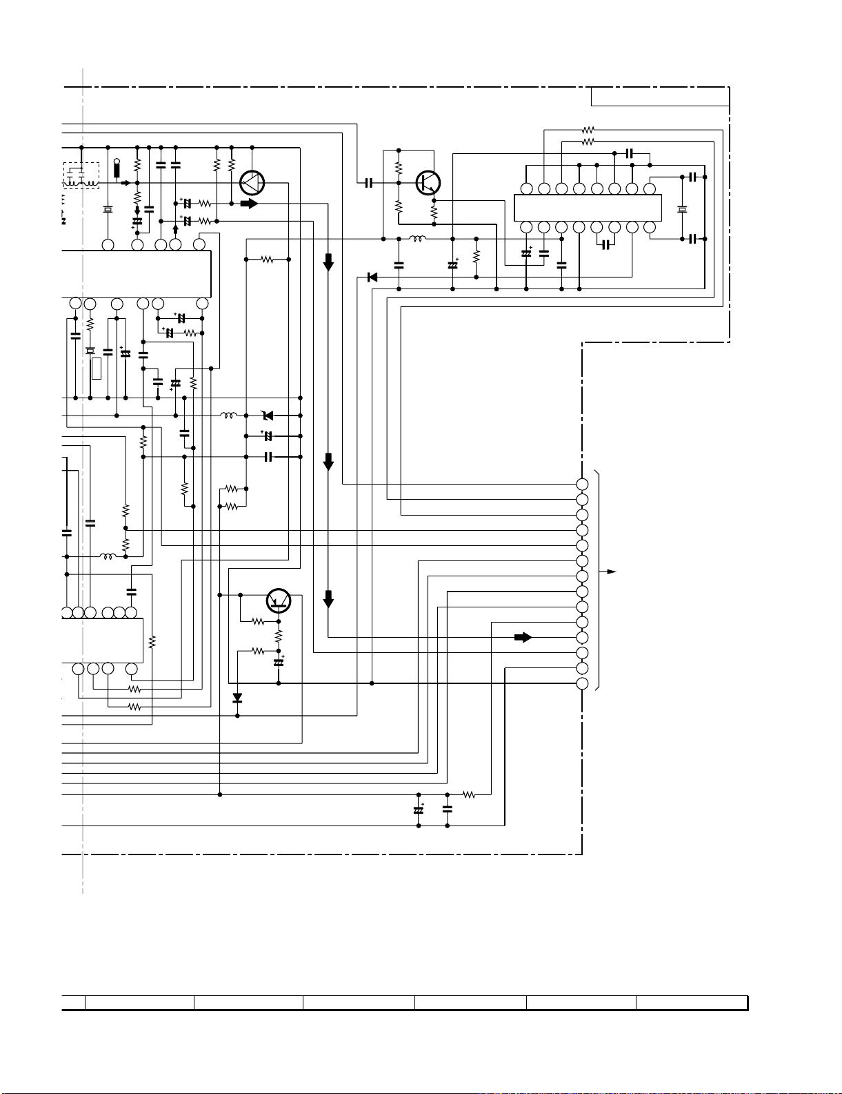
[3] SCHEMATIC DIAGRAM MAIN(1/3)
A
CD MECHANISM Ass'y(209)
FOTR-
TR+
FO+
B
C
MD
LD
ACTUATOR
VR
SHORT
LAND
F
C
B
A
D
E
CD PICKUP UNIT
D
MECHANISM PWB
E
SPINDLE
MOTOR
SLED
MOTOR
PICKUP IN
F
FO-
16
TR-
15
TR+
14
FO+
13
MD
12
VR
11
LD
10
GND
9
F
8
C
7
B
6
A
5
D
4
E
3
VCC
2
VC
1
+
SP+
1
2
3
4
5
6
1
2
3
4
5
6
CNS402
M
SP-
+
SL+
M
SL-
-
PU-IN
GND
MAIN PWB-A1(1/3)
FO-
16
TR-
15
TR+
FO+
MD
VR
LD
GND
9
F
8
C
7
B
6
A
5
D
4
E
3
VCC
2
VC
1
CNP801
SP+
1
2
SP-
3
SL+
4
SL-
5
PU-IN
6
D_GND
7
CNW402
JP801
R801
JP802
0
0
0
R802
FC801
14
13
12
11
10
8.2K
R803
8.2K
CD SIGNAL
ZD801
DZH05C2+
+B
+B
C801
0.1
330
R804
+B
C802 C803
33/16
C809
0.001
FOCUS/TRACKING/
SPIN/SLED DRIVER
R853
10K
0.1
IC802
LA6548ND
C804
CD
VIN3
RESET
REG_OUT
REG_IN
VIN2
+B
3.3
R805
Q801
2SA1235F+
0.1
R806
470
212019181716 272625 302928242322
GND
GND
789
GND
VO4-
VO1-
GND
C844
2200/16
VG4
VO4+
VG1
VO1+
C805
2200/16
VIN4
VIN1
VCC
VREF
VCC
MUTE
123456
VG3
VG2
VO3+
VO2+
101112131415
VO3-
VO2-
GND
GND
R807
100
+B
C807
+B
100/16
0.1
C808
9.1K
R812
18K
+B
R813
C81
C81
C81
C81
C81
C81
C818
0.05
2
R
R
C854
0.005
+B
+B
+B
C806
0.1
560
R814
G
KTC32
C811
0.1
ZD802
DZH04B2+
Q80
NOTES ON SCHEMATIC DIAGRAM can be found on page 6-1
H
The numbers to are waveform numbers shown in page 5-1
1
1 11
23456
Figure 6-2 SCHEMATIC DIAGRAM (1/8)
6 – 2
Page 21
XL-DAB9H
R831
100K
100P
C842
R841
2.2K
L806
1K
L805
1K
100P
C843
2.2K
R842
R823
10K
R824
10K
O_CD_DATA
O_CD_CLK
100P
C845
2.2K
R844
C823
10/16
C824
10/16
R830
L804
82
0.82µH
C830
Q805
2SC3052F+
9.1K
R812
18K
B
R813
C812
0.047
C813
0.01
0.047
C814
0.056
C815
220/16
C816
C817
0.01
C818
0.056
+B
C856
220/16
8.2K
R815
6.8K
R816
C854
0.0056
C857
0.1
C848
470/16
C849
R819
330
0.0022
3
C819
C821
0.1
R822
2.2M
C825
1/16
C826
0.047
C827
0.1
C828
0.1
4
0.1
C820
0.01
AVSS
C810
LDS
C822
1
2
3
4
5
6
7
8
9
10
11
12
13
14
15
16
17
18
19
20
100/16
+B
+B
0.1
10P
10P (CH)
(CH)
0.1
C832
+B
DOUT
DVDD
AMUTEB
8
DEFECT
PUIN
DMUTEB
C837
100/16
C835
C836
100/16
R832
82
DVSS
DVDD1.8
39
C2F
FSEQ
0.1
C834
1/16
R834
VVSS2
DVDD
+B
AVDD
SLCO
80 79 78 77 76 75 74 73 72 71 70 69 68 67 66 65 64 63 6162
EFMIN
RF
RCHO
LPF
PHLPF
AIN
CIN
BIN
DIN
FEC
RFMON
VREF
JITTC
EIN
FIN
TEC
TE
1
TEIN
LDD
FDO
TDO
AVDD
21 22 23 24 25 26 27 28 29 30 31 32 33 34 35 36 37 38 4039
+B+B
0.47/16
R825
680
R826
680
R827
68K
16.93MHz
C831
C829
X801
XIN
XVSS
XVDD
LCHO
LRVDD
XOUT
LRVSS
IC801
LC78690
MP3 DECODER
DIGITAL SIGNAL
PROCESSOR
7
2
5
6
SPDO
SLDO
PDOUT0
VVSS1
VVDD1
PCKIST
PDOUT1
+B
C833
0.1
R835
150
20K
VCOC2
DATACK
VPDOUT2
TEST1
STDATA
STREQ
TEST0
CONT0
CONT1
CONT2
VVDD3
DVDD1.8
DVSS
C838
100/16
R837
3.3K
VVDD2
VPREF2
LRSY
DATA
STCK
INTB1
INTB0
RESB
DO
DI
CL
CE
DVSS
DVDD
VVSS3
+B
60
59
58
57
56
55
54
53
52
51
50
49
48
47
46
45
44
43
42
41
0.1
C839
C840
0.1
L808
0.82µH
R840
22
9
10
11
R862
R861
R860
R859
C841
JM801
+B
+B
1K
1K
1K
1K
0.1
2K
R810
R811
2K
O_CD_RESET
I_CD_DATA
O_CD_CE
100P
100P
C847
C846
2.2K
R845
CD_L
CD_R
1
2
3
4
5
6
7
8
9
6-6 1-B~D
POWER SECTION
TO MAIN PWB(3/3)
1
R820
+B
+B +B
D805
1N4004
Q802
KTC3203 Y
811
.1
ZD802
H04B2+
D806
1N4004
L801
2.2µH
L807
0.82µH
+B
Q806
2HC1815 GR
KTC3205 Y
C853
470/16
0.1
C852
Q809
C855
Q808
2HC1815 GR
R850
1K
7
R828
47/16
10K
6.8K
R829
Q810
2HA1015 GR
ZD803
DZH09A2+
D801
1N4148
R852
1K
C851
R856
0.1
C850
R855
4.7K
1K
R854
470/16
1K
+B
R857
D802
1N4148
R833
510
1
D808 D807 D804
1N4004 1N4004 1N4004
R858
510
Q803
2HC1815 GR
CFW801B
+B
+B
+12V
CD-VCC
CD-P-GND
CD+B
GND
10
11
12
13
14
15
8 9 10 11 12
Figure 6-3 SCHEMATIC DIAGRAM (2/8)
6 – 3
Page 22
XL-DAB9H
B
(0V)
0 022
1
µ
E
R
3
5
[4] SCHEMATIC DIAGRAM MAIN(2/3)
A
FM MUTE
LEVEL
L353
1mH
R358
L321
0.82µH
CHASSIS
GND
VR351
B
5.6K
D303
1N4148
7
D304
1N4148
C301
0.001
C349
SO301
ANTENNA
TERMINAL
0.001
C388
0.001
C376
0.001
C
FROM
FM ANTENNA
FM
75 OHMS
8
FE301
FM FRONT END
9V
6
5
R369B
82
68
R369A
L342
2.2µH
C346
0.022
R345
4.7K
C345
0.022
2.5V
C348
R343
100/16
180
C341
0.022
C347
R346
330
0.022
1234
R344
680
CF301
R347
R348
6.8K
0.8V
680
9.5V
R349
Q301
33
+B
R351
CF302
FM RF
C351
2SC380 O
0.022
10.7MHz
8.2K
C344
2.1V
33P
C343
2.5V
AM OSC
FM IF
OUT
IN
33P
5V
5V
C352
C360
AM MIX
10/16
0.022
AM OSC
C361
C362
3.3/50
2.1V
IN
REG
OUT
2.1V 2.1V
321
C350
FM AFC
0.022
0.022
(2.7V)
2.1V
(2.7V)
IN
AM RF
C363
0.022
0.6V
C364
VSM
4.7/25
(0.9V)
0V
AM IF
IN
C365
AM LOW
0V
0.022
CUT
GND
LOW PASS FILT
C366
0.001
2.3V
OUT
FM/AM
SD
654
5V
C353
0.022
2.7K
R350
C367
STEREO
5V
C354
1/50
L354
87
0.022
CF351
X351
FM DET
456kHz
1718192021222324
2.3V
MPX VCO
2.9V
(4.3V)
270
R353
C399
FM IF
+
FM IF
D
C397
R382
330
R386
+B
E
FM SIGNAL
F
330
C381
12P
2.6V
(CH)
X352
4.5MHz
C382
2.6V
15P
(CH)
IC302
LC72131
C384
0.001
PLL(TUNER)
C394
0.022
47/16
10K
202122
C393
1/50
AOUT
R374
1K
0.1V
C392
R380
1.5K
DI
CE
0.1V
1K
R373
VT
R381
VSS
X OUT
XIN
0V
0.001
0.9V
4.8V
1K
R372
R
C380
10/16
0.022
C387
R379
2.2K
0.9V
PD
AIN
DO
CL
7654321
5.1V
1.7V
(11.4V)
1K
R371
5.2V
VDD
(0V)
2.6V
8
3.7V
0V
FM IN
AM IN
MUTEFMFM
9
(0V)
3.9V
C385
L3
100
(2.6V)
141516171819
10
0.01
5
MO/ST
3.5V
DO
CL
DI
CE
+B
G
H
NOTES ON SCHEMATIC DIAGRAM can be found on page 6-1
1
23456
Figure 6-4 SCHEMATIC DIAGRAM (3/8)
6 – 4
Page 23
5
2V
C387
W PASS FILTER
L354
2.7K
R350
X351
456kHz
1/50
C367
2.3V
STEREO
FM DET
87
2.9V
5V
R353
0.022
C354
FM IF
CF351
+B
R393
0.022
C385
L351
100µH
(0V)
.
0V
2.6V
(2.6V)
VDD
FM IN
AM IN
MUTE
FM
10
9
8
(0V)
3.9V
3.7V
MPX VCO
(4.3V)
270
C399
1K
0.01
R377
5.6K
MO/ST
(0V)
3.5V
R360
4.7K
(0V)
VCC
9
0.022
R359
1.8K
R356
C368
5V
C398
121314151617
11
1/50
R357
470K
C374
0.022
1K
56P
C369
1.3V
1.3V
2.1V
OUT
L-CH
R-CH
MPX IN
PHASE
IF OUT
C358
10 11 12
1/50
0V
3.8V
(1.9V)
100/10
C357
2.2/50
C356
0.001
22P
(CH)
C370
C355
47K
R395
IF INIF REQ
C386
0V
330P
R365
C383
R387
10K
C371
1/50
C372
1/50
OUT
0.022
5.6K
C373
1/50
0.022
R361
10K
R362
10K
1314151617
MO/ST
9.1K
R364
PHASE
(AM/FM)
3.8V
R355
10K
R376
R363
4V
(2.2V)
LA1832S
(1.2V)
3.3K
IC303
L352
100µH
C396
100/10
R391
390
R392
390
9.1K
+B
FM IF DET./FM MPX./AM IF
DZ5.1BSB
+B
2HA1015 GR
+B
11.7V
R383
5.6K
R384
6.8K
D308
1N4148
Q351
KRC104 M
R366
2.2K
ZD351
C395
0.022
Q360
10.9V
R385
5.6K
10.8V
C391
+B
47/16
XL-DAB9H
MAIN PWB A-1(2/3)
R529
1K
+B
R528
1.3V
0.1
FM ST
TUN_R
D_GND
A_GND
1.3V
5.1V
330P
VSM
A_12V
TUN_L
1K
0V
0V
16
17
18
SD
19
20
DO
21
CL
22
CE
23
DI
24
25
26
27
28
29
5.1V
56K
R534
2.5V
C537
0.022
D521
1N4148
VSM
A_GND
TUN L
TUN R
DATA
CLE
R533
2.2 µH
C536
0.022
56K
L521
Q521
2HC1815 GR
LC72723M
2V
10K
R532
+B
C535
IC521
RDS
R521
47/16
0V
123456 87
2.5V
2.5V
C521
10/16
47K
C522
C523
RDS_DATA
RDS_CLK
0V
2.5V
C524
560P
5.1V
0V
2.3V
0.6V
TO MAIN PWB(3/3)
C527
0.1
910111213141516
2.5V
2.5V
6-61-F
POWER SECTION
X521
456kHz
C526
22P
(CH)
C525
22P
(CH)
R342
C390
47/16
C389
10
0.047
+B
7
8 9 10 11 12
Figure 6-5 SCHEMATIC DIAGRAM (4/8)
6 – 5
Page 24

XL-DAB9H
2 2/50
K
5
1
7
8
P GND
LIN
C612
[5] SCHEMATIC DIAGRAM MAIN(3/3)
6 - 8 5~6-G
FROM DISPLAY PWB
CNS501
A
B
C
D
E
F
G
TO DISPLAY PWB
6 - 3 12-A~G
TO MAIN PWB(1/3)
CD SERVO SECTION
TO MAIN PWB(2/3)
CNP510
6-8 4 - G
6 - 5 11-C,D
TUNER SECTION
1
2
3
4
MAIN PWB-A1(3/3)
CD L
1
2
CD R
3
O_CD_RESET
4
I_CD_DATA
5
O_CD_DATA
6
O_CD_CLK
7
O_CD_CE
8
9
CFW801A
10
+12V
11
CD-VCC
12
CD-P-GND
13
CD+B
14
GND
15
VSM
16
RDS_DATA
17
RDS_CLK
18
SD
19
FM ST
20
DO
21
CL
22
CE
23
DI
24
A_12V
25
TUN_L
26
TUN_R
27
D_GND
28
A_GND
29
CNS510
DAB_+3.3V
1
2
DAB_GND
3
DAB_+5V
4
DAB_POWER
5
CNW510
CONSTANT VOLTAGE
L502
0.82µH
IC141
BAD033T++
CONSTANT VOLTAGE
REGULATOR
C190
470/6.3
3
1
2
+B
IC140
KIA7805API
REGULATOR
3
C192
470/6.3
+B
+B
2
24 8675913
O_CD_CLK
O_P_MUTE
+B
D116
1N4004
1
+B
O_CD_CE
I_CD_DATA
O_CD_DATA
O_CD_RESET
C191
470/16
O_CD+B
0_AMP_ON
FM ST
O_POWER
Q150
KTA1271 Y
R131
1.5K(1/4)
11 13 1715 1614 18 19 2010 12
SD
O_TU_CE
RDS_VSM
R130
47K
Q151
2SC3052 F+
I_TU_SDI
O_TU_SCK
RDS_DATA
O_TU_SDO
+B
M+5V
D_GND
RDS_CLK
D-GND
CNP501
2HA1015 GR
M+5V
M_GND
Q105
ZD115
DZH05C2+
R125
820
R126
330
Q109
KTC3203 Y
R127
C126
390
47/25
CNW502
CD-P-GND
D-GND
A_GND
M_GND
TO DISPLAY PWB
CNP502
6-8 5 - G
M_GND
DAB_R
CD-VCC
+B
SP-GND
CNS502
3214
3214
DAB_AGND
DAB_L
2.7K
R467
TUN L
+B
2.2K
R114
P-ON
Q106
2.7K
R468
TUN R
+B
LRVDD
3.3K
R123
2HC1815 GR
+B
1N4148
C129
2200/16
C118
D113
22/16
R110
1.5K
R117
R124
C128
R111
6.8K
R116
2.2K
0.1
680
AUX L
CD L
LC75341M
AUDIO
PROCESSOR
CD R
DAB_R
AUX R
6.8K
R.F
D114
1N4148
C119
100/16
R105
1K
R115
2.2K
Q107
2HC1815 GR
47K
R128
ZD111
DZH11B1+
C124
0.01
Q103
2SC3052 F+
DAB_L
IC601
IN1
R113
3.3K
R112
3.3K
Q108
2HC1815 GR
+B
D110
1SS133
C439
10/16
C605
C606
C601
C602
C440
R601
R602
R603
PRE.GND
IN2
4321
1/50
C125
Q101
2SB1370 E+
R118
100
EMC-GND
R604
R605
10/16
C123
R108
1K
10/16
10/16
1K
1K
10/16
10/16
1K
1K
1K
5
1/50
STBY
C120
Q102
R109
0.1
R643
100
C624
10/16
+B
+B
2SC3052 F+
L1
2.2K
6
R644
R606
P.P
2.2K
R450
1K
101112
R3R1R2R4RSL0
151413 1
1K
R607
R469
C625
10/16
VCC
7
C121
4.7/50
R120
C117
22/50
R614
10K
1K
1K
R629
8
5.6K
R628
L4L3L2
OUT2
C115
1000/2
R119
56K
1K
1716
C608
1K
D112
C607
89
4.7/50
R61
9
4.7/50
LSL0
C610
10
Q104
C609
RIN
2.2/50
1N4148
2HC1815 GR
H
NOTES ON SCHEMATIC DIAGRAM can be found on page 6-1
1
23456
Figure 6-6 SCHEMATIC DIAGRAM (5/8)
6 – 6
Page 25

XL-DAB9H
4
7/50
1K
2
2K
L2
R2
C117
RIN
LIN
D101
1N5395
1N5395
330P
C637
330P
C638
D601
L104
1µH
D102
1N5395
0.1
0.1
D104
1N5395
KTC3205 Y
C161
220/16
ZD151
FM SIGNAL
CD SIGNAL
AUX SIGNAL
DAB SIGNAL
R645
3.3K
R646
3.3K
R663
10K
C603
D602
1N4148
1N4148
C202
330P
R201
1K
R202
1K
330P
C203
D202
D201
1N4148
1N4148
C110
0.0047
R101
270
R102
270
C112
330P
D158
1N4004
Q154
2.2K
R164
C158
0.022
DZ4R7BSB
Q652
2HC1815 GR
R662
10K
Q651
R664
KRA107 M
2.7K
3
2
1
0.0047
C201
C111
330P
RP602
KTA1271 Y
2.2K
R180
C157
100/16
R665
2.7K
R661
2HC1815 GR
3.3K
0.0047
When Servicing,
Pay attention as the area enclosed
by this line ( ) is directly
connected with AC main voltage.
D105
1N4004
Q128
R162
47K
R163
2.7K
(1/4)
1
2
3
18K
R667
18K
R668
5V
CFW601
1
2
3
CNW730
1
2
3
CHASSIS
GND
J103
HEADPHONES
Q653
POWER PWB-A3
PT1
POWER TRANSFORMER
L101
LINE
FILTER
F101
T200mA L250V
SO102
AC INPUT
SOCKET
AC POWER
SUPPLY CODE
AC 230V 50Hz
SO601
LINE OUT
1
2
3
CNS730
SO201
LINE IN
CNP730
TO DISPLAY PWB
6-8 5 - B
R623
100K
C619
220P
C620
220P
C621
220P
10K
R631
4.7K
R633
R632
R630
4.7K
10K
+B
22K
R635
39K
R637
C636
100/16
R620
2.2K
R634
39K
22K
R636
R626
7.5K
C628
470P
C634
3.3/50
R619
2.2K
.
R614
10K
1K
R450
R628
1K
10
L4
L3
R3
R4
15
1K
R469
R629
C625
10/16
C611
C607
C609
4.7/50
2.2/50
1K
LIN
LSL0
RSL0
RIN
181716 212019 242322
C610
C612
C608
4.7/50
2.2/50
R615
1K
10K
R613
0.0027
R616
LTRE
RTRE
0.0027
R617 C614
2.2K
2.2K
R612
C613
0.18/63
5.6K
LBS
RBS
0.18/63
5.6K
C622
LOUT
ROUT
C623
CL
CE
DI
C615
0.1
VREF
C616
0.1
C617
1/16
VSS
1/16
33/16
123456789
DI
CE
CL
VDD
+B
C604
C618
0.047
100/16
R608
+B +B
R622
100K
220
IC101
LA4631++
C122
12
4.7/50
OUT1
(L)
(R)
POWER AMP.
13
C132
0.0047
D155
1N4004
R121
R122
3.3K
3.3K
C130
C131
0.0047
R106
10
R107
10
0.0047
GND
VP
C109
0.1
L103
R103
10
C106
C107
0.0047
C108
0.1
CNW103
1
2
3
4
5
FROM DISPLAY PWB
CNW108
1
2
L102
C105
0.1
0.0047
R104
10
C104
CNS102
6-8 4 - G
C103
0.0047
C102
0.0047
0.1
L_OUT
L_IN
R_IN
R_OUT
CNW105
CNS103
VCC
OUT2
P_GND
8
9
10
7
.
R120
22/50
C115
1000/25
R119
56K
5.6K
D112
1N4148
Q104
2HC1815 GR
11
C116
1000/25
C629
470P
R621
7.5K
C635
3.3/50
680
R639
C627
4.7/50
R OUT
1
2
3
4
J101
SPEAKER
TERMINAL
1
2
3
4
5
6
1
2
3
4
5
CNS108
212
FROM TUN1
CNW712
6-8 5 - A
+B
+B
+B
678
IC602
15234
R638
680
C630
10/16
L602
L603
3.3 µH
L201
R641
27K
L202
L203
3.3 µH
R642
27K
CHASSIS
GND
SPEAKER BOX A'SSY
SPEAKER BOX A'SSY
1
2
3
4
5
CNS105
L150
+B
CNP103
2.2 µH
GND
1
VP
2
+11.3V+11.3V
3
4
R160
5
1K
LED+11.3V
CNP102
1
VP
2
L511
+5.6V
3
D_GND
4
5
NEC_+4V
CNP108
1
C631
10/16
C633
330/16
C632
0.01
PRE.AMP.
NJM14558
C626
4.7/50
L OUT
CNW601
L601
1
3.3 µH
2
3.3 µH
3
4
3.3 µH
1
2
3.3 µH
3
4
5
CNW201
L-CH
R-CH
+B
C141
Q110
KRC107 M
C162
0.1
0.047
2
3
1
IC151
KIA7805API
CONSTANT VOLTAGE
REGULATOR
+B
3
2
C139
0.047
D109
C136
1
47/25
2
0.0047
CNP151
1N4004
C140
CNS601
1
2
3
1
2
3
4
CNS201
+B
C137
3300/35
+B
1
C138
1000/25
TO CHASSIS GND
1
R OUT
2
L OUT
3
CNP601
1
2
3
4
CNP201
CNP105
1
2
3
4
5
C101
0.047
JACK PWB-B2
D103
C133
C134
CFW101
7
8 9 10 11 12
Figure 6-7 SCHEMATIC DIAGRAM (6/8)
6 – 7
Page 26

XL-DAB9H
E
[6] SCHEMATIC DIAGRAM DISPLAY
TUN1
A
ANTENNA TERMINAL
(201-4)
CNW711
SHIELD COVER
(218)
CNW712
TO POWER PWB
CNS730
6-7 12 - C
TO JACK PWB
CNP151
6-7 9 - H
B
C
DISPLAY PWB-A2
MECHANISM PWB
SLOT IN MECHANISM UNIT (208)
DAB SIGNAL
AT24C04
EEPROM
D
SWITCH PWB-B1
E
F
G
H
CNS702
CNS705
CNS510
6-61-G
FROM MAIN PWB (3/3)
CHASSIS
GND
NOTES ON SCHEMATIC DIAGRAM can be found on page 6-1
CNP102
6-7 9 - G
TO POWER PWB
CNS102
6-6 5 - A
FROM MAIN PWB (3/3)
CNS502
CNP501
6-6 3 - A
TO MAIN PWB (3/3)
SYSTEM
MICROCOMPUT
1
23456
Figure 6-8 SCHEMATIC DIAGRAM (7/8)
6 – 8
Page 27

SD-RAM
XL-DAB9H
Except for U.K. Only
SYSTEM
OCOMPUTER
1
2
3
4
5
6
CNS703
SENSOR PWB-A4
REMOTE
SENSOR
CNW725
SHIELD
PLATE
(205-10)
7
8 9 10 11 12
Figure 6-9 SCHEMATIC DIAGRAM (8/8)
6 – 9
Page 28

XL-DAB9H
1
11
16
16 16
J
CHASSIS
GND
JACK PWB-B2 (TOP VIEW)
FC801
SPINDLE
MOTOR
SLED
MOTOR
PICKUP IN
MECHANISM PWB
564321
CD MECHANISM Ass'y(209)
CD PICKUP UNIT
DISPLAY PWB-A2 (TOP VIEW)
SWITCH PWB-B1 (TOPVIEW)
SENSOR PWB-A4 (TOPVIEW)
PH
LINE
OUT IN
CFW701
TO
CHASSIS
CNW702
CNW705
1
1
3
1
BK
BK
BK
GY
GY
GY
GY
2
123
34567
234
1
1
4
1
2345
6
7
CNS702
CNS705
13
CNP705
CNP702
CNP720
7
6
8
8
1
1
1
1
CNP701
CNP730
1
1
3
7
CNW502
1
BK
GY
2
3
4
5
6
CNS402
CNW402
1
7
CNW201
CNW601
BR
BR
WH
RD
BK
WH
WH
BK
RD
RD
BK
BK
BK
RD
WH
BK BK
RD
RD
WH
WH
1
1
5
4
1
4
2
3
CNS601
1
2
3
4
CNS201
CNP601
CNP201
CNP105
1
1
1
3
4
5
CFW601
TO
CHASSIS
1
1
BK
GY
2
3
4
5
6
7
CNW703
CNS703
CNP703
1
1
20
1
4
CNS501
CNP502
CNS730
CNW730
1
1
3
23
CNW102
CNP510
CNS102
LCD701
FL DISPLAY
1
2
CNP725
GY
BK
1
2
CNW725
Shield Plate
(205- 10)
BK
[7] WIRING SIDE OF PWB
Figure 6-10 WIRING SIDE OF PWB (1/10)
6 – 10
Page 29

XL-DAB9H
W)
3
4
CNW502
GY
RD
RD
J103
PHONES
1234
WH
WH
BK BK
ANTENNA TERMINAL
CNP501
MAIN PWB-A1 (TOPVIEW)
CNS502
BK
1
CFW801A
16
CNP801
1
CFW801B
(201-4)
20
CNS510
BK
WH
CNW711
WH
BK
BK
CNP710
TUN1
GY
DISPLAY PWB-A2 (BOTTOMVIEW)
CHASSIS
GND
CNS103
5
1
21234
BKBKBK
BK
GY
CNS108
1
5
CNW103
GY
BK
1
2
CNW108
GY
4
3
2
1
5
BK
CNW510
1
6
CNW105
1
GY
CNS105
5
4
3
2
1
BK
CHASSIS
GND
SPEAKER TERMINAL
TO
CHASSIS
FROM
FM ANTENNA
SO102
AC INPUT
SOCKET
LEFTRIGHT
BK
51
CFW101
POWER TRANSFORMER
F101
CNP102
CNW712
5
CNP103
2
1
CNP151
2
1
2
1
CNP108
1
SLOT IN MECHANISM UNIT(208)
MECHANISM PWB
Figure 6-11 WIRING SIDE OF PWB (2/10)
6 – 11
POWER PWB-A3 (TOP VIEW)
COLOR TABLE
BR
BROWN
RD(R)
RED
OR
ORANGE
YL
YELLOW
GR
GREEN
BL
BLUE
VL
VIOLET
GY
GRAY
WH(W)
WHITE
BK
BLACK
PK
PINK
Page 30

XL-DAB9H
[8] WIRING SIDE OF PWB MAIN TOP
A
B
C
MAIN PWB-A1 (TOP VIEW)
D
E
F
G
H
Lead-free solder is used in there MAIN PWB.
Refer to "Precautions for handling lead-free solder" for instructions
and precautions.
1
Lead-free solder indication
23456
Figure 6-12 WIRING SIDE OF PWB (3/10)
6 – 12
Page 31

XL-DAB9H
)
7
8 9 10 11 12
Figure 6-13 WIRING SIDE OF PWB (4/10)
6 – 13
Page 32

XL-DAB9H
[9] WIRING SIDE OF PWB MAIN BOTTOM
A
B
C
MAIN PWB-A1 (BOT
D
E
F
G
H
Lead-free solder is used in there MAIN PWB.
Refer to "Precautions for handling lead-free solder" for instructions
and precautions.
1
Lead-free solder indication
23456
Figure 6-14 WIRING SIDE OF PWB (5/10)
6 – 14
Page 33

BOTTOM VIEW)
XL-DAB9H
WAVEFORM NUMBERS
9
61
60
10
8
65
70
80
75
IC801
1
5
10
4
15
3
20
The numbers to are waveform numbers shown in page 5-1
7
8 9 10 11 12
1 11
11
55
50
45
41
40
35
30
25
6
7
21
5
2
1
Figure 6-15 WIRING SIDE OF PWB (6/10)
6 – 15
Page 34

XL-DAB9H
[10] WIRING SIDE OF PWB POWER/JACK
A
LINE
OUT IN
J103
PHONES
B
C
JACK PWB-B2 (TOP VIEW)
D
E
JACK PWB-B2 (BOTTOM VIEW)
F
G
H
Lead-free solder is used in there POWER, JACK PWB.
Refer to "Precautions for handling lead-free solder" for instructions
and precautions.
Lead-free solder indication
1
23456
Figure 6-16 WIRING SIDE OF PWB (7/10)
6 – 16
Page 35

XL-DAB9H
SO102
AC INPUT
SOCKET
POWER PWB-A3 (TOP VIEW)
When Servicing,
Pay attention as the area enclosed
by this line ( ) is directly
connected with AC main voltage.
POWER PWB-A3 (BOTTOM VIEW)
7
8 9 10 11 12
Figure 6-17 WIRING SIDE OF PWB (8/10)
6 – 17
Page 36

XL-DAB9H
A
B
C
D
E
F
G
H
1
23456
SWITCH PWB-B1 (TOP VIEW)
SENSOR PWB-A4 (TOP VIEW)
SWITCH PWB-B1 (BOTTOM VIEW)
Lead-free solder indication
Lead-free solder is used in there DISPLAY,SENSOR,SWITCH PWB.
Refer to "Precautions for handling lead-free solder" for instructions
and precautions.
[11] WIRING SIDE OF PWB DISPLAY/SWITCH
Figure 6-18 WIRING SIDE OF PWB (9/10)
6 – 18
Page 37

SENSOR PWB-A4 (BOTTOM VIEW)
XL-DAB9H
DISPLAY PWB-A2 (TOP VIEW)
7
8 9 10 11 12
Figure 6-19 WIRING SIDE OF PWB (10/10)
TUN1
For U.K.
Except for U.K.
DISPLAY PWB-A2 (BOTTOM VIEW)
6 – 19
Page 38

XL-DAB9H
CHAPTER 7. FLOWCHART
[1] TROUBLESHOOTING
1. When the CD does not function
The CD section may not operate when the objective lens of the optical pickup is dirty. Clean the objective lens, and check the playback operation.
When this section does not operate even after the above step is taken, check the following items.
Remove the cabinet and follow the trouble shooting instructions.
"Track skipping and/or no TOC (Table Of Contents) may be caused by build up of dust other foreign matter on the laser pickup lens. Before attempting
any adjustment make certain that the lens is clean. If not, clean it as mentioned below."
Turn the power off.
Gently clean the lens with a lens cleaning tissue and a small amount of isopropyl alcohol.
Do not touch the lens with the bare hand.
Parts code
1. CD optical pickup Lens cleaner disc UDSKA0004AFZZ
HOW TO USE
1.
Using the brush in the cleaner cap, apply 1 or 2 drops of the cleaning fluid to the
brush on the CD cleaner disc which has the mark next to it.
2.
Place the CD cleaner disc onto the CD disc tray with the brush side down,then
press the play button.
3.
You will hear music for about 20 seconds and the CD player will automatically stop.
If it still play continuously, press the stop button.
Cleaning fluid
CAUTION
The CD lens cleaner should be effective for 30-50 operations, however if the
brushes become worn out earlier then please replace the cleaner disc.
If the CD cleaner brushes become very wet then wipe off any excess fluid with a soft
cloth.
Do not drink the cleaner fluid or allow it contact with the eyes. In the event of this
happening then drink and / or rinse with clean water and seek medical advice.
The CD cleaner disc must not be used on car CD players or on computer CD-ROM
drives.
All rights reserved. Unauthorized duplicating, broadcasting and renting this product
is prohibited by law.
2. When a CD cannot be played
2.1. Pressing the CD operation key is accepted, but playback does not occur.
1) Focus-HF system check
2) Tracking system check
3) Spin system check
4) PLL system check
5) Others
Cleaner disc
7 – 1
Page 39

XL-DAB9H
(1) Focus-HF system check.
Although a CD is inserted and the cover is closed, "NO
DISC" is displayed.
T
1
Stopped
FDO
CH1=500 mV
DC 10:1
CH3=500 mV
DC 10:1
500 ms/div
(500 ms/div)
NORM:20 kS/s
Press the DISC EJECT switch (SW708) without inserting a disc,
and try starting the playback operation.
TDO
3
Smoothing : ON CH1 : 0.000 V
BW : FULL
CH2 : 0.0 V
CH3 : 0.000 V
CH4 : 0.00 V
=Record Length=
Main : 100 K
Zoom : 2 K
=Trigger==Filter= =Offset=
Mode : AUTO
Type : EDGE CH1
Delay : 0.0 ns
Hold off : 0.2 µs
Figure 1
1. Does the pickup move to the PICKUP-IN Switch position? No Sled motor.
Yes
2. Does the focus (lens) move up and down?
No Check the focus peripheral circuit.
(Waveform drawing Figure 1)
Yes
3. Is the laser lit? No Check the laser diode driver Q801 peripheral circuit.
CH1
v/DIV
500 mV
Yes
4. Is the turntable rotating? No Spindle motor.
When a disc is loaded, start playback operation.
1. Is focus servo activated?
(Waveform drawing Figure 2)
No Pins 5~9,11, 14 and 18,19 on IC801.
Check the laser diode driver Q801 peripheral circuit.
Yes
2. Does DRF change from "L" to "H"? No Is the disc rotating? No Check the spin system.
If the disc is spinning and a HF waveform
is generated, DRF will go H.
3. Is the HF waveform normal?
Yes
No If the level is not normal.
(Waveform drawing Figure 3)
Stopped
CH1=500 mV
CH2=10 V
DC 10:1
CH3=1 V
DC 10:1
DC 10:1
FDO
1
500 ms/div
(500 ms/div)
NORM:20 kS/s
RF
TE
3
-3 div -1 div 0 div +1 div +3 div
Smoothing : ON CH1 : 0.000 V
BW : FULL
CH Position To
CH2 : 0.0 V
CH3 : 0.00 V
CH4 : 0.00 V
=Record Length=
Main : 100 K
Zoom : 2 K
Figure 2
CH2
Position
0.20 div
=Trigger==Filter= =Offset=
Mode : AUTO
Type : EDGE CH1
Delay : 0.0 ns
Hold off : 0.2 µs
7 – 2
Figure 3
Vp-p=1.0 V~1.3 V
0.5 mV/div,0.5 µsec/div
Page 40

XL-DAB9H
(2) Tracking system check.
Check the TE waveform at pin 16 on IC 801.
If the waveform shown in Figure 4 appears and soon after NO
DISC appears?
Yes
No
"Initialization" is possible, but play is not possible?
Yes
No
"Initialization" is not possible. Data cannot be read. Check the VCO-PLL (Pin26~30 on IC801)
The tracking servo is not activated.
Check the peripheral circuits at pins 15, 16 and 23 on IC801,
and FC801.
A normal jump operation cannot be completed or the beginning
of the track cannot be found.
Check the around pin 23 on IC801.
system.
(3) Spin system check.
Press the DISC EJECT switch without inserting a disc, and
then try starting the play operation.
1. The turntable rotates a little?
(Waveform drawing Figure 5)
Yes
Stopped
CH1=10 V
DC 10:1
TE
2
Smoothing : ON CH1 : 0.0 V
BW : FULL
T
CH2=1 V
DC 10:1
CH2 : 0.00 V
CH3 : 0.00 V
CH4 : 0.00 V
The spin driver circuit is OK.
=Record Length=
Main : 100 K
Zoom : 2 K
Figure 4
100 ms/div
(100 ms/div)
NORM:100 kS/s
=Trigger==Filter= =Offset=
Mode : NORMAL
Type : EDGE CH1
Delay : 2.924 ms
Hold off : 0.2 µs
No
2. The turntable doesn't rotate. Check around pin 25 on IC801, pins 10 and 11 on IC802, and
CNW402.
Stopped
CH1=200 mV
DC 10:1
T
FDO
2
SPDO
1
=Filter= =Offset=
Smoothing : ON CH1 : 0.000 V
BW : FULL
T
CH2=500 mV
DC 10:1
CH2 : 0.000 V
CH3 : 0.00 V
CH4 : 0.00 V
=Record Length=
Main : 100 K
Zoom : 2 K
1999/04/07 09:51:15
500 ms/div
(500 ms/div)
NORM:20 kS/s
=Trigger=
Mode : NORMAL
Type : EDGE CH2
Delay : 2.924 ms
Hold off : 0.2 µs
Figure 5
7 – 3
Page 41

XL-DAB9H
(4) PLL system check.
When a disc is loaded, start play operation.
The HF waveform is normal, but the TOC data cannot be read.
Check the PDOUT waveform. (Figure 6)
Check around pins 26~30 on IC801.
Stopped
CH1=500 mV
DC 10:1
PDOUT0
3
4
PDOUT1
T
FDO
1
Smoothing : ON CH1 : 0.000 V
BW : FULL
CH2 : 0.0 V
CH3 : 0.00 V
CH4 : 0.00 V
CH3=1 V
DC 10:1
=Record Length=
Main : 100 K
Zoom : 2 K
Figure 6
1999/04/05 17:33:17
CH4=1 V
500 ms/div
(500 ms/div)
DC 10:1
NORM:20 kS/s
=Trigger==Filter= =Offset=
Mode : AUTO
Type : EDGE CH2
Delay : 0.0 ns
Hold off : 0.2 µs
CH1
v/DIV
500 mV
(5) Others.
The HF waveform is normal and the time is displayed normally, but no sound is produced. Or the sound has dropouts.
Is pin 35 (C2F) on IC801 "L"? No There are too many error flags on a damaged disc which makes
error correction impossible.
Yes
1. When playing at normal speed.
Check the peripheral circuit at pin 69 (DOUT) on IC801 and the
waveform (Figure 7).
If OK, Check the unit.
Check again using a known good disc.
T
Stopped
CH1=2 V
DC 10:1
T
1
DOUT
=Filter= =Offset=
Smoothing : ON CH1 : 0.00 V
BW : FULL
CH2 : 0.00 V
CH3 : 0.00 V
CH4 : 0.00 V
=Record Length=
Main : 1 K
Zoom : 100
Figure 7
1999/04/07 09:25:28
500 ns/div
(500 ns/div)
NORM:200 MS/s
=Trigger=
Mode : NORMAL
Type : EDGE CH1
Delay : 2.887 ms
Hold off : 0.2 µs
7 – 4
Page 42

XL-DAB9H
XL-DAB9H
CHAPTER 8. OTHERS
[1] FUNCTION TABLE OF IC
TUN1 DCEKLV596SJ01: DAB Unit (For U.K.)
TUN1 DCEKLV597SJ01: DAB Unit (Except for U.K.)
Service Manual
1. FS2023 (VOLTERRA) MODULE OVERVIEW
1.1. Intr od uc tion
The FS2023 (Volterra) module has been developed as an OEM module, which will enable low cost Band /L-Band DAB receivers. All that
is required to produce a low cost Digital Radio is a power source,
antenna, LCD and Keypad. Alternatively the module can be programmed to operate in ‘slave’ mode under the control of an existing
microcontroller. The module has been designed for use in static, portable and car audio products.
Reference software can be provided for both master (R eference MMI),
or slave (Serial Interface) applications.
1.2. Features
A block diagram of the Module is shown in Figure 7-1. The main components are Band /L-Band RF frontend, FS1010 (Chorus) DAB
baseband processor, a serial boot FLASH and audio DAC.
As an option SDRAM can be fitted to support advanced applications.
External components that may be connected to the module are shown
as grey blocks in Figure 7-1.
NOTE: 3.3 V rail is connected to RF section only and care should be
taken to provide a clean, decoupled supply to ensure that the
RF sensitivity is not degraded.
Band
L-Band RF
Serial
Flash
3.3V
/
LCD
384KB
RAM
Keypad/
Rotary
encoder
FS1010
(Chorus)
External
DAC or
CODEC
SDRAM
(optional)
Audio
DAC
The FS1010 (Chorus) processor is based around Imagination Technologies' META advanced RISC/DSP. In addition to running the core DAB
demodulation functions, this processor is well suited to running the
application code, which receiver manufacturers will add on top of the
core DAB processing to produce complete products. The core DAB
functions require less than one third of the processing capacity of
META, leaving considerable scope for application processing.
2. HARDWARE INTERFACES
The FS2023 (Volterra) module has a number of hardware interfaces,
designed to support a range of DAB applications. The characteristics
of these interfaces are detailed below.
2.1. RF Input
There are two connectors available that can be used to carry VHF (174
MHz to 240 MHz) for Band /1450 MHz to 1492 MHz for L-Band.
Thesearea2.6mmUMPtypeand2.54mmpitchholestobeused
with a header or for direct soldering of an RF cable.
Input impedance: 50 R, nominal
VSWR 2.0, maximum
Max power: 0 dBm
Sensitivity:
(signal level required for 10
Adjacent Channel Rejection
-4
(for 10
BER with 1/2 rate coding)
2.2. Analogue Audio output
Stereo line level outputs are provided using the on-board stereo audio
DAC.
2.3. Digital Audio Input/Output (I2S)
Seven signal wires (master clock, bit clock, sample frame, stereo in, 6
channel out) carry digital audio input and multi-channel output to an
external DAC or CODEC. The multi-channel output may be used for
home cinema applications including Dolby Digital and DTS.
Sample rate: 48 kHz
Master clock rate: 512 x sample r ate (24.576 MHz)
Sample resolution: 16, 18, 20 or 24 bits (controlled by software).
-4
BER with 1/2 rate coding)
-98 dBm
38 dB minimum
Serial
I/Faces
S/PDIF
&RDI
I/faces
USB
I/face
Figure 1 VOLTERRA MODULE BLOCK DIAGRAM
(Functions in white are on board, in grey are external)
An on-board SPI port supports a serial boot FLASH device.
A dedicated port is provided for direct connection to an LCD, generalpurpose I/O lines are provided for keypad scanning, shaft encoder
input and control of simple circuits.
Hardware interfaces include USB ports, and a serial host port for connection to a controlling CPU.
Stereo audio output is available in S/PDIF digital formats, as well as
line level. Multi-channel audio output is available via the I
2
S port, while
PCM or compressed audio can be input to CHORUS via the S/PDIF
input.
2.4. S/PDIF Audio Output
The S/PDIF audio output carries a stereo digital audio output on a single wire using the signal format defined in IEC60958.
Sample rate: 48 kHz
Sample resolution: 24 bits
2.5. S/PDIF Input
The S/PDIF input accepts digital audio data on a single wire using the
signal format defined in IEC60958. This input may also be used as an
input for CD-ROM data including MP3 encoded date.
2.6. RDI Output
The RDI output carries a an RDI signal conforming to Specification of
the Receiver Data Interface (RDI) - Eureka 147 Project - Issue 1. 4
November 1996 on a single wire using the signal format defined in
IEC60958. If an output is not required, then this line may be used as
GPIO.
Sample rate: 48 kHz
RDI format: high capacity
8 – 1
Page 43

XL-DAB9H
2.7. Asynchronous Serial Port
The asynchronous serial port carries asynchronous serial characters
over two wires (TxD, RxD) at data rates up to 115 kbit/s. In this particular application it can be used to control the module in ‘slave’ mode.
The default baud rate is 115 kbit/s.
2.8. Universal Serial Bus
A USB 1.1 interface (slave) is carried over two wires. The USB interface will support data transfers at up to 12 Mbits/s.
2.9. Serial Control Bus (I2C)
The Serial Control Bus consists of a two wire, open collector bus. This
bus is a master only, and may be used for controlling other devices in
the system.
2.10. PDM output
A single PDM (Pulse Density Modulated) output can be provided for
generation of a low resolution analogue output. This may be used for
control of display brightness for example.
2.11. LCD Port
LCD display data is presented on 8 data lines, with 4 timing control
lines to synchronize transfers. The LCD port will support both alphanumeric and graphic LCDs. If a LCD connection is not required, then
these lines may be used as GPIO.
Alphanumeric mode: 4-bit or 8-bit data transfers.
Compatible with displays using Hitachi
HD44780, Samsung S6A0069X (KS0066) or
similar controllers.
Graphic mode: 4-bit or 8-bit data transfers.
4 control signals (date clock, line clock, frame
clock, polarity reversal) compatible with wide
range of graphic display controllers.
NOTE: Ideally, the LCD controller should be powered from the 3V3
supply. If a 5 V LCD module is used it should have its own
supply rail and should not be connected to the 5 V RF supply
as any conducted noise will degrade RF sensitivity.
2.12. General Purpose I/O
All the above signals (excluding USB, I2S control and stereo out) may
be used as GPIO signals. The state of each GPIO signal can be read
by software. The logic level and tri-state drive of each GPIO signal can
also be controlled by software.
The following table specifies the main pin functions, identifies which of
these can be used as GPIO lines, and also defines an example DAB
product function based on the reference MMI software.
Main Function GPIO CN1 pin
number
S/PDIF Output A11 12 S/PDIF Output
S/PDIF Input A0 37 Keypad row 3
RDI Output A10 38 Keypad row 4
S1_DIN D3 15
S1_DOUT D2 16
USB_DP No 9 USB_DP
USB_DM No 8 USB_DM
SCP_CLK A9 39 IR remote activity LED
SCP_DAT A8 40 IR receiver input
PDM Output A7 41 Keypad column 3
LCD_DATA<7..0> B<15..8> 25-32 LCD_DATA<7..0>
LCD_F C1 33 Keypad row 2
LCD_LRS C2 34 LCD_RS
LCD_M C0 35 Keypad row 1
LCD_PE C3 36 LCD_E
AUD_SFR No 21 AUD_SFR
AUD_SCLK No 23 AUD_SCLK
AUD_MCLK No 24 AUD_MCLK
AUD_SDOUT0 No 22 AUD_SDOUT0
AUD_SDOUT1 A1 42 Keypad column 1
AUD_SDOUT2 A2 43 Keypad column 2
AUD_SDIN A12 44 Keypad column 4
The Reference MMI software assigns the following button mapping for
the keypad matrix:
Column 1 Column 2 Column 3 Column 4
Row 1 scroll_up scroll_down Select preset 1
Row 2 display info Scan preset 2
Row 3 volume_up volume_down Mute preset 3
Row 4 power factor y _rst preset 4 preset 5
Reference MMI
Implementation
8 – 2
Page 44

XL-DAB9H
IC601 VHiLC75341M-1: Signal Control (LC75341M)
Pin No. Terminal Name Function
1 DI Serial data and clock input pin for con-
trol.
2 CE Chip enable pin.
Data written into an internal latch in a
timing of "H" to "L".
Each analog switch is activated.
Data transfer enabled at "H" level.
3 VSS Ground pin.
4 LOUT Bass band filter comprising
capacitor and resistor connection pin
and bass/treble output pin.
5 LBASS Bass band filter comprising capacitor
and resistor connection pin.
6 LTRE Treble band filter comprising capacitor
and resistor connection pin.
7 LIN Volume + equaliser output pin.
8 LSEL0 Input selector output pin.
9,10,11,12L4-1 Input signal pin.
IC601 VHiLC75341M-1: Signal Control (LC75341M)
LIN
LSEL0
LTRE
Pin No. Terminal Name Function
13,14,
15,16
17 RSEL0 Input selector output pin.
18 RIN Volume + equaliser output pin
19 RTRE Treble band filter comprising capacitor
20 RBASS Bass band filter comprising capacitor
21 ROUT Bass band filter comprising capacitor
22 VREF 0.5x VDD voltage generation block
23 VDD Supply pin
24 CL Serial data and clock input pin for con-
R1-4 Input signal pin.
and resistor connection pin.
and resistor connection pin.
and resistor connection pin and bass/
treble output pin.
for analog ground. Capacitor of several 10µF to be connected between
VREF and AWSS (VSS) as a countermeasure against power ripple.
trol.
LOUT
LBASS
45678
L4
L3
L2
L1
R1
R2
R3
R4
9
10
11
12
13
14
15
16
CONTROL
CIRCUIT
LOGIC
CIRCUIT
CONTROL
CIRCUIT
1817
RSEL0
Figure 2 BLOCK DIAGRAM OF IC
19
RIN
RTRE
INTERFACE
CCB
20 21
RBASS
LVref
RVref
ROUT
3
2
1
24
23
22
VSS
CE
DI
CL
VDD
VREF
8 – 3
Page 45

IC701 RH-iXA063SJ00: System Microcomputer (IXA063SJ)
Pin No Port Name Terminal Name Input/Output Function
1* PA1 2* PA2 -
3 PA3/AN12 PROG_ENA Input PROGRAM USE DATA1/ENABLE(PULL-UP NEED)
4* PA4/AN13 PROG_DAT Input/Output PROGRAM USE DATA0
5* PA5/AN14 PROG_CLK Input/Output PROGRAM USE CLOCK
6 P70/INT0/T0LCP/AN8 I_HOLD Input [INT] BACKUP
7 P71/INT1/T0HCP/AN9 I_KEY3 Input [INT/AD] KEY INPUT FOR TIMER/SLEEP
8 P72/INT2/T0IN I_POWER Input [INT] KEY INPUT FOR POWER KEY
9 P73/INT3/T0IN I_REM Input [INT] REMOTE SIGNAL INPUT
10 RES - Input RESET
11 XT1/AN10 - - SUB CLOCK
12 XT2/AN11 - - f=32.768KHz
13 VSS1 GND - GND
14 CF1 - - MAIN CLOCK
15 CF2 - - f=8MHz
16 VDD1 VDD1 - +5.0V
17 P80/AN0 I_KEY1 Input [A/D] KEY INPUT
18 P81/AN1 I_KEY2 Input [A/D] KEY INPUT
19 P82/AN2 I_RDS_VSM Input [A/D] RDS VSM DETECT
20 P83/AN3 I_TU_SD Input TUNER SD INPUT
21 P84/AN4 I_FM_ST Input FM STEREO INPUT
22 P85/AN5 I_VOL_ENC Input [A/D] VOL ENCODER INPUT
23 P86/AN6 I_SUFIX (MATRIX) Input [A/D] DIFFERENT COUNTRY SELECT
24 P87/AN7 DAB_KEY Input [A/D] DAB KEY INPUT
25* P30/PMW4 -
26 P31/PMW5 I_DAB_MUTE Input DECTION_DAB_MUTE
27 P32/UTX1 O_P_MUTE Output AMP INPUT MUTE (H:ON)
28 P33/URX1 O_CD_RESET Output CD RESET
29 P34 O_CD_CE Output CD-CE
30 P10/SO0 O_CD_DATA Output CD DATA OUT(LC78690 DATA IN)
31 P11/SI0/SB0 I_CD_DATA Input CD DATA INPUT(LC78690 DATAOUT)
32 P12/SCK0 O_CD_CLK Output CD CLOCK(LC78690 DATA IN)
33 P13/SO1 O_LCD_DATA Output ST 7032 SI(DB7)
34 P14/SI1/SB1 O_LCD_CSB Output ST 7032 CSB
35 P15/SCK1 O_LCD_CLK Output ST7032 CLOCK(DB6)
36 P16/T1PWML O_LCD_RS Output ST7032 RS
37 P17/T1PWMH/BUZ O_LCD_RESET Output ST7032 RESET
38 SI2P0/DO2 O_DAB_DATA Output DAB DATA OUT(uPD78006)
39 SI2P1/SI2/SB2 I_DAB_DATA Input DAB DATA IN(uPD78006)
40 SI2P2/SCK2 I_DAB_CLK Input DAB CLOCK IN(uPD78006)
41 SI2P3/SCK20 O_DAB_EN Output DAB_ENABLE_OUT
42 PWM1 O_DAB_ONOFF Output DAB ON/OFF
43 PWM0 O_DAB_RESET Output DAB_RESET
44 VDD2 VDD2 - +5.0V
45 VSS2 GND - GND
46 P00 O_POWER Output POWER SWITCH
47 P01 O_AMP_ON Output AMP ON
48 P02 O_CD_ON Output CD POWER ON
49 P03 SW1 Input SLOT IN TRAY POSITON DETECT
50 P04 SW2+4 Input SLOT IN TRAY POSITON DETECT
51 P05/CK0 SW3 Input SLOT IN TRAY POSITON DETECT
52 P06/T6O MM+ Output SLOT-IN MECHA CONTROL
53 P07/T7O MM- Output SLOT-IN MECHA CONTROL
54 P20/INT4 RDS_CLK Input [INT] RDS CLK SIGNAL (LC72723)
55 P21/INT4 RDS_DATA Input RDS DATA IN (LC72723)
56 P22/INT4 O_EEP_CLK Output EEPROM CLOCK
57 P23/INT4 IO_EEP_DATA Input/Output EEPROM DATA
58 P24/INT5 O_TU_DATA Output TU DATA OUT (LC72131, LC75341 DATA IN)
59 P25/INT5 I_TU_DATA Input TUNER DATA INPUT (LC72131 DATA OUT)
60 P26/INT5 O_TU_CLK Output CLOCK (LC72131, LC75341 CLOCK IN)
61 P27/INT5 O_TU_CE Output CHIP SELECT (LC72131, LC75341)
62* PB7 Output
63* PB6 Output
XL-DAB9H
8 – 4
Page 46

XL-DAB9H
Pin No Port Name Terminal Name Input/Output Function
64* PB5 Output
65* PB4 Output
66* PB3 Output
67* PB2 Output
68* PB1 Output
69 PB0 LINE_OUT_MUTE Output
70 VSS3 GND - GND
71 VDD3 VDD3 - +5.0V
72* PC7 Output
73* PC6 Output
74* PC5 Output
75* PC4 Output
76* PC3 Output
77* PC2 Output
78* PC1 Output
79* PC0 Output
80 PA0 LED_CON Output LED CONTROL
In this unit, the terminal with asterisk mark (*) is (open) terminal which is not connected to the outside.
IC701 RH-iXA063SJ00: System Microcomputer (IXA063SJ)
Figure 3 BLOCK DIAGRAM OF IC
8 – 5
Page 47

IC702 RH-iXA066SJ00: SD-RAM,(IXA066SJ)
Pin No Port Name Terminal Name Input/Output Function
1 P50/A8 A_MUTE Output Audio(DAB) mute(H:DAB MUTE ON)
2* P51/A9 3* P52/A10 4* P53/A11 5* P54/A12 6* P55/A13 -
7 P56/A14 DAB POWER Output DAB Power control(H;off) to HOST
8* P57/A15 -
9Vsso Vsso -
10 Vddo Vddo 11* P30 12* P31 HS - (HS: For flash writer)
13* P32 14* P33 -
15 P34/SI3/TxD2 SI3 Output For flash writer
16 P35/SO3/RxD2 SO3 Output For flash writer
17 P36/SCK3/ASCK2 SCK3 Output For flash writer
18 P20/SI1 SI Input HOST Interface DATA(HOST)
19* P21/SO1 SO Output HOST Interface DATA(DAB)
20 P22/SCK1 SCK Output HOST Interface CLK(DAB)
21 P23/Rxd0 S1_DIN Input DAB RXD
22 P24/TxD0 S1_DOUT Output DAB TXD
23 P25/ASCK0 SCP_CLK Output DAB Handshake
24
25
V
AV
DD1
SS
-
-
26* P17/ANI7 27* P16/ANI6 28* P15/ANI5 29* P14/ANI4 30* P13/ANI3 31* P12/ANI2 32* P11/ANI1 33* P10/ANI0 -
34
AV
REF
-
35* P80/SS1 -
36 RESET - RESET from HOST
37* XT2 38* XT1 -
39 IC - IC/VPP(FLASH: 10k pull down, MASK: GND)
40 X2 OSC - 8.38MHz
41 X1 OSC - 8.38MHz
42
V
SS1
-
43 P00/INTP0 EN - HOST Interface EN(HOST)
44 P01/INTP1 PON_DET - Power key detect
45* P02/INTP2 46* P03/INTP3 47* P70/TI000/T000 48* P71/TI010 49* P72/TI50/TO50 50* P73/TI51/TO51 51* P74/PCL/TI011 52* P75/BUZ/TI001/TO01 53* P64/RE 54* P65/WR -
55 P66/WAIT SDRAM_SEL Input SDRAM select(H:8M, L:64M)
56 P67/ASTB MODE_SEL Input MODE(Destination) select(H:Dual Band, L:Band3)
57* P40/AD0 58* P41/AD1 59* P42/AD2 60* P43/AD3 61* P44/AD4 62* P45/AD5 63* P46/AD6 -
XL-DAB9H
8 – 6
Page 48

XL-DAB9H
Pin No Port Name Terminal Name Input/Output Function
64* P47/AD7 -
In this unit, the terminal with asterisk mark (*) is (open) terminal which is not connected to the outside.
IC702 RH-iXA066SJ00:SD-RAM, (IXA066SJ)
P72/TI50/TO50
P73/TI51/TO51
P74/PCL/TI011
P64/RD
P65/WR
P66/WAIT
P67/ASTB
P40/AD0
P41/AD1
P42/AD2
P43/AD3
P45/AD5
P44/AD4
P46/AD6
P47/AD7
P75/BU2/TI001/TO01
P50/A8
P51/A9
P52/A10
P53/A11
P54/A12
P55/A13
P56/A14
P57/A15
VSS0
VDD0
P30
P31
P32
P33
P34/SI3/TxD2
P35/SO3/RxD2
1
2
3
4
5
6
7
8
9
10
11
12
13
14
15
16
AVSS
P24/TxD0
P23/RxD0
P22/SCK1
VDD1
P25/ASCK0
P17/ANI7
P16/ANI6
P15/ANI5
P14/ANI4
P13/ANI3
P20/SI1
P21/SO1
P36/SCK3/ASCK2
Figure 4 BLOCK DIAGRAM OF IC
505152535455565758596061626364 49
313029282726252423222120191817 32
P12/ANI2
48
47
46
45
44
43
42
41
40
39
38
37
36
35
34
33
P11/ANI1
P71/TI010
P70/TI000/TO00
P03/INTP3/ADTRG
P02/INTP2
P01/INTP1
P00/INTP0
VSS1
X1
X2
IC
XT1
XT2
RESET
P80/SS1
AVREF
P10/ANI0
8 – 7
Page 49

XL-DAB9H
IC801 VHiLC7890/-1: MP3 Decoder Digital Signal Processor (LC78690)
Pin No. Terminal Name Input/Output Setting in Reset Function
1 EFMIN Input Input RF signal input.
2 RFOUT Output Unfix RF signal output.
3 LPF Output Unfix To LPF capacitor for detecting DC level of RF signal.
4 PHLPF Output Unfix To LPF capacitor for detecting scratch.
5 AIN Input Input A signal input.
6 CIN Input Input C signal input.
7 BIN Input Input B signal input.
8 DIN Input Input D signal input.
9 FEC Output Unfix To LPF capacitor for FE signal.
10* RFMON Output Unfix Monitoring for LSI internal analog signal.
11 VREF Output AVDD/2 VREF voltage output.
12 JITTC Output Unfix For jitter detection capacitor.
13 EIN Input Input E signal input.
14 FIN Input Input F signal input.
15 TEC Output Unfix To LPF capacitor for TE signal.
16 TE Output Unfix TE signal output.
17 TEIN Input Input TE signal input for TES signal generation.
18 LDD Output Unfix Laser power control signal output.
19 LDS Input Input Laser power detection signal input.
20 AVSS - - Analog GND. Connected to 0V.
21 AVDD - - Analog power supply.
22 FDO Output AVDD/2 Focus control signal output. D/A output.
23 TDO Output AVDD/2 Tracking control signal output. D/A output.
24 SLDO Output AVDD/2 Sled control signal output. D/A output.
25 SPDO Output AVDD/2 Spindle control signal output. D/A output.
26 VVSS1 - - For EFM
27 PDOUT1 Output Unfix Phase comparison output pin 1 for built-in VCO control.
28 PDOUT0 Output Unfix Phase comparison output pin 0 for built-in VCO control.
29 PCKIST Input Input To resistance for current setting of PDOUT0, 1 output.
30 VVDD1 - - Power supply for built-in VCO
31* DMUTEB Output L DMUTEB (general-purpose) output
32 PUIN Input/Output Input PUIN (general-purpose) input/output (Built-in Pull-Up resistance)
33* DEFECT Output L Scratch detection signal output
34* FSEQ Output L Sync signal output. Switches to "H" when sync signal detected from EFM
35* C2F Output L C2 error signal output.
36 DVDD - - Digital power supply.
37 DVSS - - Digital GND. Connected to 0V.
38 DVDD1.8 Output H To power supply capacitor for digital circuit.
39 VVDD3 - - Power supply for built-in PLL.
40 VVSS3 - - GND for built-in PLL. Connected to 0V.
41 DVDD - - Digital power supply.
42 DVSS - - Digital GND. Connected to 0V.
43 CE Input Input For micro44 CL Input Input Data transfer clock input.
45 DI Input Input Data input
46 DO Output (H) Data output (Tri-state output: Built-in Pull-Up resistance)
47 RESB Input - Reset input for this LSI. Set as "L" when turning power on.
48* INTB0 Output H Interrupt signal output pin 0 (Servo section)
49* INTB1 Output H Interrupt signal output pin 1 (Decoder section)
50 CONT2 Input/Output Input General-purpose input/
51* CONT1 Input/Output Input General-purpose input/
52* CONT0 Input/Output Input General-purpose input/
53 TEST0 Input L Input for testing. Connected to 0V.
54 STREQ Input/Output Input Stream data request signal output.
55 STCK Input/Output Input Bit clock input for stream data.
56 STDATA Input/Output Input Stream data input.
57 TEST1 Input L Input for testing. Connected to 0V.
58* DATA Output L L/R channel data output.
59* DATACK Output L Bit clock output
PLL
signal and sync signal generated internally are the same.
processor
interface
output pin 2
output pin 1
output pin 0 (Built-in PullUp resistance)
GND for built-in VCO. Connected to 0V.
Enable signal input.
Controlled by command from microprocessor.
When not in use, set as input and connect to
0V, or set as output and leave open.
8 – 8
Page 50

XL-DAB9H
Pin No. Terminal Name Input/Output Setting in Reset Function
60* LRSY Output L L/R ch clock output
61 VVDD2 - - For EFM
62 VPREF2 Input Input Input for oscillation range setting of built-in VCO.
PLL
63 VCOC2 Input Input Input for control voltage setting of built-in VCO.
64 VPDOUT2 Output Unfix Output for controlling built-in VCO.
65 VVSS2 - - GND for built-in VCO. Connected to 0V.
66 DVDD1.8 Output H To power supply capacitor for digital circuit.
67 DVSS - - Digital GND. Connected to 0V.
68 DVDD - - Digital power supply.
69* DOUT Output L Digital OUT output. EIAJ format.
70* AMUTEB Output L AMUTEB (general-purpose) output.
71 XVSS - - Digital GND. Connected to 0V.
72 XOUT Output Oscillator For crystal
73 XIN Input Oscillator
oscillation
74 XVDD - - Digital power supply
75 LCHO Output LRVDD/2 D/A con76 LRVDD - - Power supply for LR channel.
verter
77 LRVSS - - GND for LR channel. Connected to 0V.
78 RCHO Output LRVDD/2 R channel output.
79 AVDD - - Analog power supply.
80 SLCO Output Unfix Slice level control output.
In this unit, the terminal with asterisk mark (*) is (open) terminal which is not connected to the outside.
IC801 VHiLC7890/-1: MP3 Decoder Digital Signal Processor (LC78690)
Power supply for built-in VCO
To 16.9344 MHz oscillator
L channel output.
EFMIN
RFOUT
LPF
PHLPF
AIN
CIN
BIN
DIN
FEC
RFMON
VREF
JITTC
EIN
FIN
TEC
TE
TEIN
LDD
LDS
AVSS
1
2
3
4
5
6
7
8
9
10
11
12
13
14
15
16
17
18
19
20
SLCO
AVDD
RCHO
79 78 77 76 75
80
SLICE LEVEL
CONTROL
RF
SIGNAL
PROCESSOR
VREF
MONITOR
TES, HFL,
DEFECT
JITTER
APC
LRVSS
LPF
LRVDD
LCHO
XVDD
XIN
73 72 71
74
CLOCK
GENERATOR
1bit DAC
8FS DIGITAL FILTER
DEEMPHASIS
ATTENUATION CONTROL
INTERPOLATION MUTE
Synchronization
Detection
EFM
Demodulation
SERVO
CONTROL
A/D
D/A
CD PLL
XOUT
XVSS
AMUTEB
DOUT
68
70
69
DOUT
Audio FLT MUTE
MP3 & WMA
DECODER
Memory I/F
TEXT
SUBCODE DECODE
DVDD
DVSS
DVDD1.8
66
67
ROM
DECODER
ERROR
CORRECTION
VVSS2
65
VCOC2
VPDOUT2
64
63
PLL2
Memory
CONTROL
VPREF2
62
AUDIO
I/F
Stream
I/F
1M
CPU I/F
&
PORT
PLL3
VVDD2
61
60
LRSY
59
DATACK
58
DATA
57
TEST1
56
STDATA
55
STCK
54
STREQ
53
TEST0
52
CONT0
51
CONT1
50
CONT2
49
INTB1
48
INTB0
47
RESB
46
DO
45
DI
44
CL
43
CE
42
DVSS
41
DVDD
21
22 23 24 25 26 27 28 29 30 31 32 33 34 35 36 37 38 39 40
AVDD
FDO
TDO
SLDO
SPDO
VVSS1
PDOUT1
PDOUT0
VVDD1
PCKIST
PUIN
DMUTEB
FSEQ
DEFECT
C2F
DVDD
DVSS
Figure 5 BLOCK DIAGRAM OF IC
8 – 9
VVDD3
DVDD1.8
VVSS3
Page 51

[2] FL DISPLAY
LCD701: RV-LXA010SJZZ
XL-DAB9H
ICON
Address
00H
01H
02H
03H
04H
05H
06H
07H
08H
09H
0AH
0BH
0CH
0DH
0EH
0FH
1 2 3
00H 01H 02H 03H 04H 05H 06H 07H 08H 09H 0AH 0BH 0CH 0DH 0EH 0FH
40H 41H 42H 43H 44H 45H 46H 47H 48H 49H 4AH 4BH 4CH 4DH 4EH 4FH
2
1
ICON RAM bits
D7 D6 D5 D4 D3 D2 D1 D0
4 5
6 7 8 9
1 2
1
2
3
4
5
6
7
8
9
8 – 10
Page 52

XL-DAB9H
-MEMO-
8 – 11
Page 53

PartsGuide
XL-DAB9H
PARTS GUIDE
MICRO COMPONENT SYSTEM
[1] INTEGRATED CIRCUITS
[2] TRANSISTORS
[3] DIODES
[4] FILTERS
[5] TRANSFORMERS
[6] COILS
[7] VIBRATORS
[8] CAPACITORS
[9] RESISTORS
MODEL
XL-DAB9H Micro Component System consisting of
XL-DAB9H (main unit) and CP-DAB9H (speaker system).
CONTENTS
[10] OTHER CIRCUITRY PARTS
[11] CABINET PARTS
[12] SPEAKER BOX PARTS
[13] ACCESSORIES/PACKING PARTS
[14] ACCESSORIES/PACKING PARTS
[15] P.W.B. ASSEMBLY (Not
[16] OTHER SERVICE PARTS
XL-DAB9H
(Except for U.K.)
(For U.K.)
Replacement Item)
INDEX
Parts marked with " " are important for maintaining the safety of the set. Be sure to replace these
parts with specified ones for maintaining the safety and performance of the set.
This document has been published to be used
for after sales service only.
The contents are subject to change without notice.
Page 54

XL-DAB9H
NO. PARTS CODE
PRICE
RANK
NEW
MARK
PAR T
RANK
DESCRIPTION
[1] INTEGRATED CIRCUITS
IC7A1 VHIAT24C04/-1 AH EEPROM,AT24C04
IC140 VHIKIA7805API AF Constant Voltage Regulator,KIA7805API
IC141 VHIBA033T++-1 AK Constant Voltage Regulator,BA033T++
IC151 VHIKIA7805API AF Constant Voltage Regulator,KIA7805API
IC302 VHILC72131/-1 AP PLL (Tuner),LC72131
IC303 VHILA1832S/-1 AN FM IF Det./FM Mpx./AM IF,LA1832S
IC521 VHILC72723M-1 AS RDS,LC72723M
IC601 VHILC75341M-1 AM Signal Control Audio Processor,LC75341M
IC602 VHINJM14558-1 AF Pre. Amp.,NJM14558
IC701 RH-IXA063SJ00 BD System Microcomputer,IXA063SJ
IC702 RH-IXA066SJ00 BC SD-RAM,IXA066SJ
IC801 VHILC78690/-1 BE MP3 Decoder Digital Signal Processor,LC78690
IC802 VHILA6548ND-1 AL Focus/Tracking/Spin/Sled Driver,LA6548ND
[2] TRANSISTORS
Q101 VS2SB1370E+-1 AG Silicon,PNP,2SB1370 E+
Q102 VS2SC3052F+-1 AD Silicon,NPN,2SC3052 F+
Q103 VS2SC3052F+-1 AD Silicon,NPN,2SC3052 F+
Q104 VS2HC1815GR-1 AB Silicon,NPN,2HC1815 GR
Q105 VS2HA1015GR-1 AB Silicon,PNP,2HA1015 GR
Q106 VS2HC1815GR-1 AB Silicon,NPN,2HC1815 GR
Q107 VS2HC1815GR-1 AB Silicon,NPN,2HC1815 GR
Q108 VS2HC1815GR-1 AB Silicon,NPN,2HC1815 GR
Q109 VSKTC3203Y/-1 AC Silicon,NPN,KTC3203 Y
Q110 VSKRC107M//-1 AC Digital,NPN,KRC107 M
Q128 VSKTA1271Y/-1 AC Silicon,PNP,KTA1271 Y
Q150 VSKTA1271Y/-1 AC Silicon,PNP,KTA1271 Y
Q151 VS2SC3052F+-1 AD Silicon,NPN,2SC3052 F+
Q154 VSKTC3205Y/-1 AD Silicon,NPN,KTC3205 Y
Q301 VS2SC380-O/-1 AC Silicon,NPN,2SC380 O
Q351 VSKRC104M//-1 AC Digital,NPN,KRC104 M
Q360 VS2HA1015GR-1 AB Silicon,PNP,2HA1015 GR
Q521 VS2HC1815GR-1 AB Silicon,NPN,2HC1815 GR
Q651 VSKRA107M//-1 AE Digital,PNP,KRA107 M
Q652 VS2HC1815GR-1 AB Silicon,NPN,2HC1815 GR
Q653 VS2HC1815GR-1 AB Silicon,NPN,2HC1815 GR
Q701 VSKTA1271Y/-1 AC Silicon,PNP,KTA1271 Y
Q702 VS2HC1815GR-1 AB Silicon,NPN,2HC1815 GR
Q703 VS2HC1815GR-1 AB Silicon,NPN,2HC1815 GR
Q704 VSKTA1271Y/-1 AC Silicon,PNP,KTA1271 Y
Q705 VSKTC3203Y/-1 AC Silicon,NPN,KTC3203 Y
Q706 VSKTC3203Y/-1 AC Silicon,NPN,KTC3203 Y
Q707 VS2SC3052F+-1 AD Silicon,NPN,2SC3052 F+
Q708 VS2HC1815GR-1 AB Silicon,NPN,2HC1815 GR
Q709 VS2SC3052F+-1 AD Silicon,NPN,2SC3052 F+
Q710 VS2SC3052F+-1 AD Silicon,NPN,2SC3052 F+
Q801 VS2SA1235F+-1 AD Silicon,PNP,2SA1235 F+
Q802 VSKTC3203Y/-1 AC Silicon,NPN,KTC3203 Y
Q803 VS2HC1815GR-1 AB
Q805 VS2SC3052F+-1 AD Silicon,NPN,2SC3052 F+
Q806 VS2HC1815GR-1 AB Silicon,NPN,2HC1815 GR
Q808 VS2HC1815GR-1 AB Silicon,NPN,2HC1815 GR
Q809 VSKTC3205Y/-1 AD Silicon,NPN,KTC3205 Y
Q810 VS2HA1015GR-1 AB Silicon,PNP,2HA1015 GR
Silicon,NPN,2HC1815 GR
[3] DIODES
D101 VHD1N5395//-1 AB Silicon,1N5395
D102 VHD1N5395//-1 AB Silicon,1N5395
D103 VHD1N5395//-1 AB Silicon,1N5395
D104 VHD1N5395//-1 AB Silicon,1N5395
D105 VHD1N4004//-1 AB Silicon,1N4004
D109 VHD1N4004//-1 AB Silicon,1N4004
D110 VHD1SS133//-1 AA Silicon,1SS133
D112 VHD1N4148//-1 AA Silicon,1N4148
D113 VHD1N4148//-1 AA Silicon,1N4148
D114 VHD1N4148//-1 AA Silicon,1N4148
D116 VHD1N4004//-1 AB Silicon,1N4004
D155 VHD1N4004//-1 AB Silicon,1N4004
D158 VHD1N4004//-1 AB Silicon,1N4004
D201 VHD1N4148//-1 AA Silicon,1N4148
D202 VHD1N4148//-1 AA Silicon,1N4148
D303 VHD1N4148//-1 AA Silicon,1N4148
D304 VHD1N4148//-1 AA Silicon,1N4148
D308 VHD1N4148//-1 AA Silicon,1N4148
D521 VHD1N4148//-1 AA Silicon,1N4148
D601 VHD1N4148//-1 AA Silicon,1N4148
D602 VHD1N4148//-1 AA Silicon,1N4148
D701 VHDDS1SS133-1 AB Silicon,DS1SS133
D702 VHDDS1SS133-1 AB Silicon,DS1SS133
D703 VHD1N4148//-1 AA Silicon,1N4148
D704 VHD1N4148//-1 AA Silicon,1N4148
D705 VHD1N4148//-1 AA Silicon,1N4148
D706 VHD1N4148//-1 AA Silicon,1N4148
D707 VHD1N4148//-1 AA Silicon,1N4148
D708 VHD1N4148//-1 AA Silicon,1N4148
2
Page 55

XL-DAB9H
NO. PARTS CODE
PRICE
RANK
NEW
MARK
PAR T
RANK
[3] DIODES
D709 VHD1N4148//-1 AA Silicon,1N4148
D801 VHD1N4148//-1 AA Silicon,1N4148
D802 VHD1N4148//-1 AA Silicon,1N4148
D804 VHD1N4004//-1 AB Silicon,1N4004
D805 VHD1N4004//-1 AB Silicon,1N4004
D806 VHD1N4004//-1 AB Silicon,1N4004
D807 VHD1N4004//-1 AB Silicon,1N4004
D808 VHD1N4004//-1 AB Silicon,1N4004
LED701 VHPLPBB73VQ-1 AF LED,White,LPBB73VQ
LED702 VHPLPBB73VQ-1 AF LED,White,LPBB73VQ
ZD111 VHEDZH11B1+-1 AB Zener,10V,DZH11B1+
ZD115 VHEDZH05C2+-1 AB Zener,5.1V,DZH05C2+
ZD151 VHEDZ4R7BSB-1 AB Zener,4.7V,DZ4.7BSB
ZD351 VHEDZ5R1BSB-1 AC Zener,5.1V,DZ5.1BSB
ZD801 VHEDZH05C2+-1 AB Zener,5.1V,DZH05C2+
ZD802 VHEDZH04B2+-1 AB Zener,3.9V,DZH04B2
ZD803 VHEDZH09A2+-1 AB Zener,8.2V,DZH09A2+
[4] FILTERS
CF301 RFILFA001SJZZ AE FM IF
CF302 RFILF0004SJZZ AG FM RF,10.7 MHz
CF351 RFILF0003AWZZ AK FM IF
[5] TRANSFORMERS
!
PT1 RTRNPA052SJZZ N Power
[6] COILS
!
L101 RCILZ0005SJZZ AF Line Filter
L102 RCILZA001SJZZ AC Line Filter
L103 RCILZA001SJZZ AC Line Filter
L104 VP-DH1R0K0000 AC 1 µ H
L150 VP-DH2R2K0000 AB 2.2 µ H,Peaking
L201 RCILCA004SJZZ AB 3.3 µ H
L202 RCILCA004SJZZ AB 3.3 µ H
L203 RCILCA004SJZZ AB 3.3 µ H
L321 VP-DHR82K0000 AE 0.82 µ H,Choke
L342 VP-DH2R2K0000 AB 2.2 µ H,Peaking
L351 VP-DH101K0000 AB 100 µ H,Choke
L352 VP-DH101K0000 AB 100 µ H,Choke
L353 VP-DH102K0000 AB 1 mH,Choke
L354 RFILL0001SJZZ AF Low Pass Filter
L502 VP-DHR82K0000 AE 0.82 µ H,Choke
L511 RCILCA004SJZZ AB 3.3 µ H
L521 VP-DH2R2K0000 AB 2.2 µ H,Peaking
L601 RCILCA004SJZZ AB 3.3 µ H
L602 RCILCA004SJZZ AB 3.3 µ H
L603 RCILCA004SJZZ AB 3.3 µ H
L703 VP-DHR47K0000 AB 0.47 µ H
L710 VP-DH101K0000 AB 100 µ H,Choke
VP-DH2R2K0000 AB 2.2 µ H,Peaking
L801
L804 VP-DHR82K0000 AE 0.82 µ H,Choke
L805 RBLN-A003SJZZ AB Ferrite Bead,1 kohms
L806 RBLN-A003SJZZ AB Ferrite Bead,1 kohms
L807 VP-DHR82K0000 AE 0.82 µ H,Choke
L808 VP-DHR82K0000 AE 0.82 µ H,Choke
[7] VIBRATORS
X351 RCRM-0007SJZZ AG VCO,456 kHz
X352 RCRSP0006SJZZ AF Crystal,4.5 MHz
X521 RCRSP0005SJZZ AF Crystal,456 kHz
X701 RCRM-0008SJZZ AG Ceramic,8 MHz
X702 RCRSP0007SJZZ AE Crystal,32.768 kHz
X703 RCRM-0008SJZZ AG Ceramic,8 MHz
X801 RCRSP0002SJZZ AL Crystal,16.93 MHz
[8] CAPACITORS
C7A1 VCKYCY1EF104Z AA 0.1 µ F,25V
C101 VCKYCY1EF473Z AB 0.047 µ F,25V
C102 VCKYCY1HB472K AA 0.0047 µ F,50V
C103 VCKYCY1HB472K AA 0.0047 µ F,50V
C104 VCKYCY1EF104Z AA 0.1 µ F,25V
C105 VCKYCY1EF104Z AA 0.1 µ F,25V
C106 VCKYCY1HB472K AA 0.0047 µ F,50V
C107 VCKYCY1HB472K AA 0.0047 µ F,50V
C108 VCKYCY1EF104Z AA 0.1 µ F,25V
C109 VCKYCY1EF104Z AA 0.1 µ F,25V
C110 VCKYCY1HB472K AA 0.0047 µ F,50V
C111 VCKYPA1HB331K AA 330 pF,50V
C112 VCKYCY1HB331K AA 330 pF,50V
C115 RC-GZV108AF1E AD 1000 µ F,25V,Electrolytic
C116 RC-GZV108AF1E AD 1000 µ F,25V,Electrolytic
C117 RC-GZA226AF1H AB 22 µ F,50V,Electrolytic
C118 RC-GZA226AF1C AB 22 µ F,16V,Electrolytic
C119 RC-GZA107AF1C AB 100 µ F,16V,Electrolytic
DESCRIPTION
3
Page 56

XL-DAB9H
NO. PARTS CODE
PRICE
RANK
NEW
MARK
PAR T
RANK
[8] CAPACITORS
C120 VCKYCY1EF104Z AA 0.1 µ F,25V
C121 RC-GZA475AF1H AB 4.7 µ F,50V,Electrolytic
C122 RC-GZA475AF1H AB 4.7 µ F,50V,Electrolytic
C123 RC-GZA105AF1H AB 1 µ F,50V,Electrolytic
C124 VCKYCY1HB103K AA 0.01 µ F,50V
C125 RC-GZA105AF1H AB 1 µ F,50V,Electrolytic
C126 RC-GZA476AF1E AB 47 µ F,25V,Electrolytic
C128 VCKYCY1EF104Z AA 0.1 µ F,25V
C129 RC-GZV228AF1C AG 2200 µ F,16V,Electrolytic
C130 VCKYCY1HB472K AA 0.0047 µ F,50V
C131 VCKYCY1HB472K AA 0.0047 µ F,50V
C132 VCKYCY1HB472K AA 0.0047 µ F,50V
C133 VCKYCY1EF104Z AA 0.1 µ F,25V
C134 VCKYPA1HB104K AC 0.1 µ F,50V
C136 VCKYCY1HB472K AA 0.0047 µ F,50V
C137 RC-GZW338AF1V AH 3300 µ F,35V,Electrolytic
C138 RC-GZV108AF1E AD 1000 µ F,25V,Electrolytic
C139 VCKYCY1HB473K AB 0.047 µ F,50V
C140 RC-GZA476AF1E AB 47 µ F,25V,Electrolytic
C141 VCKYCY1HB473K AB 0.047 µ F,50V
RC-GZA107AF1C AB 100 µ F,16V,Electrolytic
C157
C158 VCKYCY1HF223Z AA 0.022 µ F,50V
C161 RC-GZA227AF1C AB 220 µ F,16V,Electrolytic
C162 VCKYCY1EF104Z AA 0.1 µ F,25V
C190 RC-GZA477AF0J AB 470 µ F,6.3V,Electrolytic
C191 RC-GZA477AF1C AC 470 µ F,16V,Electrolytic
C192 RC-GZA477AF0J AB 470 µ F,6.3V,Electrolytic
C201 VCKYCY1HB472K AA 0.0047 µ F,50V
C202 VCKYCY1HB331K AA 330 pF,50V
C203 VCKYCY1HB331K AA 330 pF,50V
C301 VCKYCY1HB102K AA 0.001 µ F,50V
C341 VCKYCY1EF223Z AB 0.022 µ F,25V
C343 VCCSCY1HL330J AD 33 pF,50V
C344 VCCSCY1HL330J AD 33 pF,50V
C345 VCKYCY1EF223Z AB 0.022 µ F,25V
C346 VCKYCY1EF223Z AB 0.022 µ F,25V
C347 VCKYCY1EF223Z AB 0.022 µ F,25V
C348 RC-GZA107AF1C AB 100 µ F,16V,Electrolytic
C349 VCKYCY1HB102K AA 0.001 µ F,50V
C350 VCKYCY1EF223Z AB 0.022 µ F,25V
C351 VCKYCY1EF223Z AB 0.022 µ F,25V
C352 RC-GZA106AF1C AB 10 µ F,16V,Electrolytic
C353 VCKYCY1EF223Z AB 0.022 µ F,25V
C354 VCKYCY1EF223Z AB 0.022 µ F,25V
C355 VCCCCY1HH220J AA 22 pF (CH),50V
C356 VCKYCY1HB102K AA 0.001 µ F,50V
C357 RC-GZA225AF1H AB 2.2 µ F,50V,Electrolytic
C358 RC-GZA105AF1H AB 1 µ F,50V,Electrolytic
C360 VCKYCY1EF223Z AB 0.022 µ F,25V
C361 VCKYCY1EF223Z AB 0.022 µ F,25V
C362 RC-GZA335AF1H AB 3.3 µ F,50V,Electrolytic
C363 VCKYCY1EF223Z AB 0.022 µ F,25V
C364 RC-GZA475AF1E AB 4.7 µ F,25V,Electrolytic
C365 VCKYCY1EF223Z AB 0.022 µ F,25V
C366 VCKYCY1HB102K AA 0.001 µ F,50V
C367 RC-GZA105AF1H AB 1 µ F,50V,Electrolytic
C368 RC-GZA105AF1H AB 1 µ F,50V,Electrolytic
C369 VCCSCY1HL560J AD 56 pF,50V
C370 RC-GZA105AF1H AB 1 µ F,50V,Electrolytic
C371 RC-GZA105AF1H AB 1 µ F,50V,Electrolytic
C372 RC-GZA105AF1H AB 1 µ F,50V,Electrolytic
C373 VCTYPA1CX223K AA 0.022 µ F,16V
C374 VCTYPA1CX223K AA 0.022 µ F,16V
C376 VCKYCY1HB102K AA 0.001 µ F,50V
C380 RC-GZA106AF1C AB 10 µ F,16V,Electrolytic
C381 VCCCCY1HH120J AA 12 pF (CH),50V
C382 VCCCCY1HH150J AA 15 pF (CH),50V
C383 VCKYCY1EF223Z AB 0.022 µ F,25V
C384 VCKYCY1HB102K AA 0.001 µ F,50V
C385 VCKYPA1HF103Z AB 0.01 µ F,50V
C386 VCKYPA1HB331K AA 330 pF,50V
C387 VCKYCY1EF223Z AB 0.022 µ F,25V
C388 VCKYCY1HB102K AA 0.001 µ F,50V
C389 VCKYPA1HF473Z AB 0.047 µ F,50V
C390 RC-GZA476AF1C AB 47 µ F,16V,Electrolytic
C391 RC-GZA476AF1C AB 47 µ F,16V,Electrolytic
C392 VCKYCY1HB102K AA 0.001 µ F,50V
C393 RC-GZA105AF1H AB 1 µ F,50V,Electrolytic
C394 RC-GZA476AF1C AB 47 µ F,16V,Electrolytic
C395 VCKYCY1EF223Z AB 0.022 µ F,25V
C396 RC-GZA107AF1A AB 100 µ F,10V,Electrolytic
C397 VCKYCY1EF223Z AB 0.022 µ F,25V
C398 RC-GZA107AF1A AB 100 µ F,10V,Electrolytic
C399 VCKYPA1HF223Z AB 0.022 µ F,50V
C439 RC-GZA106AF1C AB
10 µ F,16V,Electrolytic
DESCRIPTION
4
Page 57

XL-DAB9H
NO. PARTS CODE
PRICE
RANK
NEW
MARK
PAR T
RANK
[8] CAPACITORS
C440 RC-GZA106AF1C AB 10 µ F,16V,Electrolytic
C521 RC-GZA106AF1C AB 10 µ F,16V,Electrolytic
C522 VCKYPA1HB331K AA 330 pF,50V
C523 VCKYCY1EF104Z AA 0.1 µ F,25V
C524 VCKYCY1HB561K AA 560 pF,50V
C525 VCCCCY1HH220J AA 22 pF (CH),50V
C526 VCCCCY1HH220J AA 22 pF (CH),50V
C527 VCKYCY1EF104Z AA 0.1 µ F,25V
C535 RC-GZA476AF1C AB 47 µ F,16V,Electrolytic
C536 VCKYCY1EF223Z AB 0.022 µ F,25V
C537 VCKYPA1HF223Z AB 0.022 µ F,50V
C601 RC-GZA106AF1C AB 10 µ F,16V,Electrolytic
C602 RC-GZA106AF1C AB 10 µ F,16V,Electrolytic
C603 VCKYCY1HB472K AA 0.0047 µ F,50V
C604 VCKYCY1EF473Z AB 0.047 µ F,25V
C605 RC-GZA106AF1C AB 10 µ F,16V,Electrolytic
C606 RC-GZA106AF1C AB 10 µ F,16V,Electrolytic
C607 RC-GZA475AF1H AB 4.7 µ F,50V,Electrolytic
C608 RC-GZA475AF1H AB 4.7 µ F,50V,Electrolytic
C609 RC-GZA225AF1H AB 2.2 µ F,50V,Electrolytic
C610 RC-GZA225AF1H AB 2.2 µ F,50V,Electrolytic
C611 VCKYCY1HB272K AA 0.0027 µ
C612 VCKYCY1HB272K AA 0.0027 µ F,50V
C613 VCQYKA1JM184J AC 0.18 µ F,63V
C614 VCQYKA1JM184J AC 0.18 µ F,63V
C615 RC-GZA105AF1C AB 1 µ F,16V,Electrolytic
C616 RC-GZA105AF1C AB 1 µ F,16V,Electrolytic
C617 RC-GZA336AF1C AB 33 µ F,16V,Electrolytic
C618 RC-GZA107AF1C AB 100 µ F,16V,Electrolytic
C619 VCKYCY1HB221K AA 220 pF,50V
C620 VCKYCY1HB221K AA 220 pF,50V
C621 VCKYCY1HB221K AA 220 pF,50V
C622 VCKYCY1HB104K AD 0.1 µ F,50V
C623 VCKYCY1HB104K AD 0.1 µ F,50V
C624 RC-GZA106AF1C AB 10 µ F,16V,Electrolytic
C625 RC-GZA106AF1C AB 10 µ F,16V,Electrolytic
C626 RC-GZA475AF1H AB 4.7 µ F,50V,Electrolytic
C627 RC-GZA475AF1H AB 4.7 µ F,50V,Electrolytic
C628 VCKYCY1HB471K AA 470 pF,50V
C629 VCKYCY1HB471K AA 470 pF,50V
C630 RC-GZA106AF1C AB 10 µ F,16V,Electrolytic
C631 RC-GZA106AF1C AB 10 µ F,16V,Electrolytic
C632 VCKYCY1EF103Z AA 0.01 µ F,25V
C633 RC-GZA337AF1C AC 330 µ F,16V,Electrolytic
C634 RC-GZA335AF1H AB 3.3 µ F,50V,Electrolytic
C635 RC-GZA335AF1H AB 3.3 µ F,50V,Electrolytic
C636 RC-GZA107AF1C AB 100 µ F,16V,Electrolytic
C637 VCKYCY1HB331K AA 330 pF,50V
C638 VCKYCY1HB331K AA 330 pF,50V
C701 RC-GZA476AF1C AB 47 µ F,16V,Electrolytic
C702 VCKYCY1HB473K AB 0.047 µ F,50V
C703 VCKYCY1HB101K AB 100 pF,50V
C705 VCKYCY1HB101K AB 100 pF,50V
C706 VCCCCY1HH200J AA 20 pF (CH),50V
C707 VCCCCY1HH200J AA 20 pF (CH),50V
C708 VCKYCY1EB101K AA 100 pF,25V
C710 VCKYCY1EF104Z AA 0.1 µ F,25V
C711 VCKYCY1HB102K AA 0.001 µ F,50V
C713 RC-EZD336AF1C AB 33 µ F,16V,Electrolytic
C714 VCKYCY1EF104Z AA 0.1 µ F,25V
C717 RC-GZA227AF1A AB 220 µ F,10V,Electrolytic
C718 VCKYCY1HB103K AA 0.01 µ F,50V
C719 VCKYCY1EB101K AA 100 pF,25V
C720 VCKYCY1EB101K AA 100 pF,25V
C721 VCKYCY1EF223Z AB 0.022 µ F,25V
C725 VCKYCY1EF223Z AB 0.022 µ F,25V
C726 VCKYCY1HF224Z AB 0.22 µ F,50V
C727 VCKYCY1HF224Z AB 0.22 µ
C728 VCKYCY1EF223Z AB 0.022 µ F,25V
C730 RC-EZD107AF0J AC 100 µ F,6.3V,Electrolytic
C731 RC-EZD107AF0J AC 100 µ F,6.3V,Electrolytic
C732 VCKYCY1HB271K AA 270 pF,50V
C733 VCKYCY1HB271K AA 270 pF,50V
C734 VCKYCY1HB271K AA 270 pF,50V
C735 VCKYCY1HB102K AA 0.001 µ F,50V
C736 VCKYCY1HB271K AA 270 pF,50V
C737 VCKYCY1HF104Z AB 0.1 µ F,50V
C738 VCKYCY1EB101K AA 100 pF,25V
C740 VCKYCY1EB101K AA 100 pF,25V
C741 VCKYCY1HB103K AA 0.01 µ F,50V
C742 VCKYCY1EB101K AA 100 pF,25V
C743 VCKYCY1HB103K AA 0.01 µ F,50V
C744 VCKYCY1HB103K AA 0.01 µ F,50V
C744 VCKYCY1HB331K AA 330 pF,50V
C745 VCKYCY1HB103K AA 0.01 µ F,50V
F,50V
F,50V
DESCRIPTION
5
Page 58

XL-DAB9H
NO. PARTS CODE
PRICE
RANK
NEW
MARK
PAR T
RANK
[8] CAPACITORS
C745 VCKYCY1HB331K AA 330 pF,50V
C746 VCKYCY1HB103K AA 0.01 µ F,50V
C746 VCKYCY1HB331K AA 330 pF,50V
C747 VCKYCY1HB103K AA 0.01 µ F,50V
C748 VCKYCY1HB103K AA 0.01 µ F,50V
C749 VCKYCY1HB103K AA 0.01 µ F,50V
C750 VCKYCY1HB103K AA 0.01 µ F,50V
C751 VCKYCY1HB103K AA 0.01 µ F,50V
C752 VCKYCY1HB103K AA 0.01 µ F,50V
C753 VCKYCY1HB103K AA 0.01 µ F,50V
C754 VCKYCY1HB103K AA 0.01 µ F,50V
C755 VCKYCY1HB103K AA 0.01 µ F,50V
C756 VCKYCY1HB103K AA 0.01 µ F,50V
C757 VCKYCY1HB103K AA 0.01 µ F,50V
C758 VCKYCY1HB103K AA 0.01 µ F,50V
C759 VCKYCY1HB103K AA 0.01 µ F,50V
C760 VCKYCY1HB103K AA 0.01 µ F,50V
C761 VCKYCY1HB103K AA 0.01 µ F,50V
C762 VCKYCY1HB103K AA 0.01 µ F,50V
C763 VCKYCY1HB472K AA 0.0047 µ F,50V
C764 VCKYCY1HB103K AA 0.01 µ F,50V
C765 VCKYCY1HB472K AA 0.0047 µ F,50V
C801 VCKYCY1EF104Z AA 0.1 µ F,25V
C802 RC-EZD336AF1C AB 33 µ F,16V,Electrolytic
C803 VCKYCY1EF104Z AA 0.1 µ F,25V
C804 VCKYCY1EF104Z AA 0.1 µ F,25V
C805 RC-GZV228AF1C AG 2200 µ F,16V,Electrolytic
C806 VCKYCY1EF104Z AA 0.1 µ F,25V
C807 RC-GZA107AF1C AB 100 µ F,16V,Electrolytic
C808 VCKYCY1EF104Z AA 0.1 µ F,25V
C809 VCKYCY1HB102K AA 0.001 µ F,50V
C810 RC-GZA474AF1C AB 0.47 µ F,16V,Electrolytic
C811 VCKYCY1EF104Z AA 0.1 µ F,25V
C812 VCKYCY1EF473Z AB 0.047 µ F,25V
C813 VCKYCY1EF103Z AA 0.01 µ F,25V
C814 VCKYCY1EF473Z AB 0.047 µ F,25V
C815 VCKYPA1HB563K AC 0.056 µ F,50V
C816 RC-GZA227AF1C AB 220 µ F,16V,Electrolytic
C817 VCKYCY1EF103Z AA 0.01 µ F,25V
C818 VCKYCY1EB563K AD 0.056 µ F,25V
C819 VCKYCY1EF104Z AA 0.1 µ F,25V
VCKYCY1EF103Z AA 0.01 µ F,25V
C820
C821 VCKYCY1HB222K AA 0.0022 µ F,50V
C822 RC-GZA107AF1C AB 100 µ F,16V,Electrolytic
C823 RC-GZA106AF1C AB 10 µ F,16V,Electrolytic
C824 RC-GZA106AF1C AB 10 µ F,16V,Electrolytic
C825 RC-GZA105AF1C AB 1 µ F,16V,Electrolytic
C826 VCKYCY1EF473Z AB 0.047 µ F,25V
C827 VCKYCY1EF104Z AA 0.1 µ F,25V
C828 VCKYCY1EF104Z AA 0.1 µ F,25V
C829 VCCCCY1HH100J AA 10 pF (CH),50V
C830 VCKYCY1HB104K AD 0.1 µ F,50V
C831 VCCCCY1HH100J AA 10 pF (CH),50V
C832 VCKYCY1HB104K AD 0.1 µ F,50V
C833 VCKYCY1HB104K AD 0.1 µ F,50V
C834 RC-GZA105AF1C AB 1 µ F,16V,Electrolytic
C835 VCKYCY1HB104K AD 0.1 µ F,50V
C836 RC-EZD107AF1C AC 100 µ F,16V,Electrolytic
C837 RC-EZD107AF1C AC 100 µ F,16V,Electrolytic
C838 RC-GZA107AF1C AB 100 µ F,16V,Electrolytic
C839 VCKYCY1HB104K AD 0.1 µ F,50V
C840 VCKYCY1HB104K AD 0.1 µ F,50V
VCKYCY1HB104K AD 0.1 µ F,50V
C841
C842 VCKYPA1HB101K AA 100 pF,50V
C843 VCKYPA1HB101K AA 100 pF,50V
C844 RC-GZV228AF1C AG 2200 µ F,16V,Electrolytic
C845 VCCSCY1HL101J AA 100 pF,50V
C846 VCCSCY1HL101J AA 100 pF,50V
C847 VCKYPA1HB101K AA 100 pF,50V
C848 RC-GZA477AF1C AC 470 µ F,16V,Electrolytic
C849 VCKYCY1EF104Z AA 0.1 µ F,25V
C850 RC-GZA477AF1C AC 470 µ F,16V,Electrolytic
C851 VCKYCY1EF104Z AA 0.1 µ F,25V
C852 VCKYCY1EF104Z AA 0.1 µ F,25V
C853 RC-GZA477AF1C AC 470 µ F,16V,Electrolytic
C854 VCKYCY1HB562K AA 0.0056 µ F,50V
C855 RC-GZA476AF1C AB 47 µ F,16V,Electrolytic
C856 RC-GZA227AF1C AB 220 µ F,16V,Electrolytic
C857 VCKYPA1HB104K AC 0.1 µ F,50V
DESCRIPTION
6
Page 59

XL-DAB9H
NO. PARTS CODE
PRICE
RANK
NEW
MARK
PAR T
RANK
[9] RESISTORS
JP710 VRS-CY1JB000J AA 0 ohm,Jumper,0.8x1.55mm,Green
JP712 VRS-CY1JB000J AA 0 ohm,Jumper,0.8x1.55mm,Green
JP713 VRS-CY1JB000J AA 0 ohm,Jumper,0.8x1.55mm,Green
JP801 VRS-CY1JB000J AA 0 ohm,Jumper,0.8x1.55mm,Green
JP802 VRS-CY1JB000J AA 0 ohm,Jumper,0.8x1.55mm,Green
R7A2 VRS-CY1JB103J AA 10 kohm,1/16W
R7A4 VRS-CY1JB103J AA 10 kohm,1/16W
R101 VRD-ST2CD271J AA 270 ohms,1/6W
R102 VRD-ST2CD271J AA 270 ohms,1/6W
R103 VRD-ST2CD100J AA 10 ohm,1/6W
R104 VRD-ST2CD100J AA 10 ohm,1/6W
R105 VRS-CY1JB102J AA 1 kohm,1/16W
R106 VRD-ST2CD100J AA 10 ohm,1/6W
R107 VRD-ST2CD100J AA 10 ohm,1/6W
R108 VRS-CY1JB102J AA 1 kohm,1/16W
R109 VRS-CY1JB101J AA 100 ohm,1/16W
R110 VRS-CY1JB152J AA 1.5 kohms,1/16W
R111 VRS-CY1JB681J AA 680 ohms,1/16W
R112 VRS-CY1JB332J AA 3.3 kohms,1/16W
R113 VRS-CY1JB332J AA 3.3 kohms,1/16W
R114 VRD-ST2CD222J AA 2.2 kohms,1/6W
R115 VRD-ST2CD222J AA 2.2 kohms,1/6W
R116 VRS-CY1JB222J AA 2.2 kohms,1/16W
R117 VRD-ST2CD682J AA 6.8 kohms,1/6W
R118 VRS-CY1JB101J AA 100 ohm,1/16W
R119 VRS-CY1JB563J AA 56 kohms,1/16W
R120 VRS-CY1JB562J AA 5.6 kohms,1/16W
R121 VRD-ST2CD332J AA 3.3 kohms,1/6W
R122 VRD-ST2CD332J AA 3.3 kohms,1/6W
R123 VRD-ST2CD332J AA 3.3 kohms,1/6W
R124 VRD-ST2CD682J AA 6.8 kohms,1/6W
R125 VRD-ST2EE821J AA 820 ohms,1/4W
R126 VRS-CY1JB331J AA 330 ohms,1/16W
R127 VRD-ST2EE391J AA
R128 VRD-ST2CD473J AA 47 kohms,1/6W
R130 VRS-CY1JB473J AA 47 kohms,1/16W
R131 VRD-ST2EE152J AA 1.5 kohms,1/4W
R160 VRS-CY1JB102J AA 1 kohm,1/16W
R162 VRS-CY1JB473J AA 47 kohms,1/16W
R163 VRD-ST2EE272J AA 2.7 kohms,1/4W
R164 VRD-ST2EE222J AA 2.2 kohms,1/4W
R180 VRD-ST2EE222J AA 2.2 kohms,1/4W
R201 VRS-CY1JB102J AA 1 kohm,1/16W
R202 VRS-CY1JB102J AA 1 kohm,1/16W
R342 VRD-ST2EE100J AA 10 ohm,1/4W
R343 VRD-ST2CD181J AA 180 ohms,1/6W
R344 VRS-CY1JB681J AA 680 ohms,1/16W
R345 VRS-CY1JB472J AA 4.7 kohms,1/16W
R346 VRS-CY1JB331J AA 330 ohms,1/16W
R347 VRS-CY1JB682J AA 6.8 kohms,1/16W
R348 VRS-CY1JB681J AA 680 ohms,1/16W
R349 VRS-CY1JB330J AA 33 ohms,1/16W
R350 VRS-CY1JB272J AA 2.7 kohms,1/16W
R351 VRS-CY1JB562J AA 5.6 kohms,1/16W
R353 VRS-CY1JB271J AA 270 ohms,1/16W
R355 VRS-CY1JB332J AA 3.3 kohms,1/16W
R356 VRS-CY1JB102J AA 1 kohm,1/16W
R357 VRS-CY1JB474J AA 470 kohms,1/16W
R358 VRS-CY1JB822J AA 8.2 kohms,1/16W
R359 VRS-CY1JB182J AA 1.8 kohms,1/16W
R360 VRS-CY1JB472J AA 4.7 kohms,1/16W
R361 VRS-CY1JB103J AA 10 kohm,1/16W
R362 VRS-CY1JB103J AA 10 kohm,1/16W
R363 VRD-ST2CD912J AA 9.1 kohms,1/6W
R364 VRS-CY1JB912J AA 9.1 kohms,1/16W
R365 VRS-CY1JB103J AA 10 kohm,1/16W
R366 VRS-CY1JB222J AA 2.2 kohms,1/16W
R369A
R369B VRS-CY1JB820J AA 82 ohms,1/16W
VRS-CY1JB680J AA 68 ohms,1/16W
R371 VRS-CY1JB102J AA 1 kohm,1/16W
R372 VRS-CY1JB102J AA 1 kohm,1/16W
R373 VRS-CY1JB102J AA 1 kohm,1/16W
R374 VRS-CY1JB102J AA 1 kohm,1/16W
R376 VRD-ST2CD103J AA 10 kohm,1/6W
R377 VRD-ST2CD562J AA 5.6 kohms,1/6W
R379 VRS-CY1JB222J AA 2.2 kohms,1/16W
R380 VRD-ST2CD152J AA 1.5 kohms,1/6W
R381 VRS-CY1JB103J AA 10 kohm,1/16W
R382 VRD-ST2EE331J AA 330 ohms,1/4W
R383 VRS-CY1JB562J AA 5.6 kohms,1/16W
R384 VRD-ST2CD682J AA 6.8 kohms,1/6W
R385 VRD-ST2CD562J AA 5.6 kohms,1/6W
R386 VRD-ST2EE331J AA 330 ohms,1/4W
R387 VRD-ST2CD562J AA 5.6 kohms,1/6W
R391 VRD-ST2EE391J AA 390 ohms,1/4W
390 ohms,1/4W
DESCRIPTION
7
Page 60

XL-DAB9H
NO. PARTS CODE
PRICE
RANK
NEW
MARK
PAR T
RANK
[9] RESISTORS
R392 VRD-ST2EE391J AA 390 ohms,1/4W
R393 VRS-CY1JB102J AA 1 kohm,1/16W
R395 VRD-ST2CD473J AA 47 kohms,1/6W
R450 VRS-CY1JB102J AA 1 kohm,1/16W
R467 VRS-CY1JB272J AA 2.7 kohms,1/16W
R468 VRS-CY1JB272J AA 2.7 kohms,1/16W
R469 VRS-CY1JB102J AA 1 kohm,1/16W
R521 VRD-ST2CD473J AA 47 kohms,1/6W
R528 VRS-CY1JB102J AA 1 kohm,1/16W
R529 VRS-CY1JB102J AA 1 kohm,1/16W
R532 VRS-CY1JB103J AA 10 kohm,1/16W
R533 VRS-CY1JB563J AA 56 kohms,1/16W
R534 VRS-CY1JB563J AA 56 kohms,1/16W
R601 VRD-ST2CD102J AA 1 kohm,1/6W
R602 VRD-ST2CD102J AA 1 kohm,1/6W
R603 VRD-ST2CD102J AA 1 kohm,1/6W
R604 VRS-CY1JB102J AA 1 kohm,1/16W
R605 VRS-CY1JB102J AA 1 kohm,1/16W
R606 VRS-CY1JB102J AA 1 kohm,1/16W
R607 VRS-CY1JB102J AA 1 kohm,1/16W
R608 VRD-ST2CD221J AA 220 ohms,1/6W
R612 VRS-CY1JB222J AA 2.2 kohms,1/16W
R613 VRS-CY1JB222J AA 2.2 kohms,1/16W
R614 VRS-CY1JB103J AA 10 kohm,1/16W
R615 VRS-CY1JB103J AA 10 kohm,1/16W
R616 VRS-CY1JB562J AA 5.6 kohms,1/16W
R617 VRS-CY1JB562J AA 5.6 kohms,1/16W
R619 VRS-CY1JB222J AA 2.2 kohms,1/16W
R620 VRS-CY1JB222J AA 2.2 kohms,1/16W
R621 VRS-CY1JB752J AA 7.5 kohms,1/16W
R622 VRS-CY1JB104J AA 100 kohm,1/16W
R623 VRS-CY1JB104J AA 100 kohm,1/16W
R626 VRS-CY1JB752J AA 7.5 kohms,1/16W
R628 VRS-CY1JB102J AA
R629 VRS-CY1JB102J AA 1 kohm,1/16W
R630 VRS-CY1JB103J AA 10 kohm,1/16W
R631 VRD-ST2CD103J AA 10 kohm,1/6W
R632 VRS-CY1JB472J AA 4.7 kohms,1/16W
R633 VRS-CY1JB472J AA 4.7 kohms,1/16W
R634 VRS-CY1JB223J AA 22 kohms,1/16W
R635 VRS-CY1JB223J AA 22 kohms,1/16W
R636 VRS-CY1JB393J AA 39 kohms,1/16W
R637 VRS-CY1JB393J AA 39 kohms,1/16W
R638 VRS-CY1JB681J AA 680 ohms,1/16W
R639 VRS-CY1JB681J AA 680 ohms,1/16W
R641 VRS-CY1JB273J AA 27 kohms,1/16W
R642 VRS-CY1JB273J AA 27 kohms,1/16W
R643 VRS-CY1JB222J AA 2.2 kohms,1/16W
R644 VRS-CY1JB222J AA 2.2 kohms,1/16W
R645 VRS-CY1JB332J AA 3.3 kohms,1/16W
R646 VRS-CY1JB332J AA 3.3 kohms,1/16W
R661 VRS-CY1JB332J AA 3.3 kohms,1/16W
R662 VRS-CY1JB103J AA 10 kohm,1/16W
R663 VRS-CY1JB103J AA 10 kohm,1/16W
R664 VRS-CY1JB272J AA 2.7 kohms,1/16W
R665 VRS-CY1JB272J AA 2.7 kohms,1/16W
R667 VRS-CY1JB183J AA 18 kohms,1/16W
R668 VRS-CY1JB183J AA 18 kohms,1/16W
R701A VRS-CY1JB471J AA 470 ohms,1/16W
R701B VRS-CY1JB471J AA 470 ohms,1/16W
R702A VRS-CY1JB391J AA 390 ohms,1/16W
R702B VRS-CY1JB391J AA 390 ohms,1/16W
R703 VRD-ST2CD102J AA 1 kohm,1/6W
R703A VRS-CY1JB223J AA 22 kohms,1/16W
R703B VRS-CY1JB223J AA 22 kohms,1/16W
R704 VRD-ST2CD102J AA 1 kohm,1/6W
R705 VRD-ST2CD102J AA 1 kohm,1/6W
VRD-ST2CD102J AA 1 kohm,1/6W
R706
R707 VRD-ST2CD102J AA 1 kohm,1/6W
R708 VRS-CY1JB102J AA 1 kohm,1/16W
R709 VRD-ST2CD102J AA 1 kohm,1/6W
R710 VRS-CY1JB102J AA 1 kohm,1/16W
R710A VRS-CY1JB103J AA 10 kohm,1/16W [Except for U.K.]
R711 VRD-ST2CD102J AA 1 kohm,1/6W
R711A VRS-CY1JB102J AA 1 kohm,1/16W [For U.K. Only]
R712 VRS-CY1JB102J AA 1 kohm,1/16W
R713 VRD-ST2CD102J AA 1 kohm,1/6W
R714 VRS-CY1JB102J AA 1 kohm,1/16W
R715 VRS-CY1JB102J AA 1 kohm,1/16W
R716 VRS-CY1JB102J AA 1 kohm,1/16W
R717 VRD-ST2CD102J AA 1 kohm,1/6W
R718 VRS-CY1JB913J AA 91 kohms,1/16W
R719 VRD-ST2CD102J AA 1 kohm,1/6W
R720 VRS-CY1JB102J AA 1 kohm,1/16W
R721 VRS-CY1JB102J AA 1 kohm,1/16W
1 kohm,1/16W
DESCRIPTION
8
Page 61

XL-DAB9H
NO. PARTS CODE
PRICE
RANK
NEW
MARK
PAR T
RANK
[9] RESISTORS
R722 VRD-ST2CD102J AA 1 kohm,1/6W
R723 VRS-CY1JB103J AA 10 kohm,1/16W
R724 VRS-CY1JB103J AA 10 kohm,1/16W
R725 VRS-CY1JB102J AA 1 kohm,1/16W
R726 VRS-CY1JB102J AA 1 kohm,1/16W
R729 VRS-CY1JB103J AA 10 kohm,1/16W
R730 VRS-CY1JB103J AA 10 kohm,1/16W
R731 VRS-CY1JB103J AA 10 kohm,1/16W
R732 VRS-CY1JB104J AA 100 kohm,1/16W
R733 VRS-CY1JB334J AA 330 kohms,1/16W
R734 VRS-CY1JB103J AA 10 kohm,1/16W
R735 VRS-CY1JB103J AA 10 kohm,1/16W
R736 VRS-CY1JB103J AA 10 kohm,1/16W
R737 VRS-CY1JB394J AA 390 kohms,1/16W
R738 VRS-CY1JB103J AA 10 kohm,1/16W
R739 VRS-CY1JB103J AA 10 kohm,1/16W
R740 VRS-CY1JB103J AA 10 kohm,1/16W
R741 VRS-CY1JB104J AA 100 kohm,1/16W
R742 VRS-CY1JB122J AA 1.2 kohms,1/16W
R743 VRS-CY1JB222J AA 2.2 kohms,1/16W
R744 VRS-CY1JB272J AA 2.7 kohms,1/16W
R745 VRS-CY1JB472J AA 4.7 kohms,1/16W
R746 VRS-CY1JB822J AA 8.2 kohms,1/16W
R747 VRS-CY1JB122J AA 1.2 kohms,1/16W
R748 VRS-CY1JB222J AA 2.2 kohms,1/16W
R750 VRD-ST2EE221J AA 220 ohms,1/4W
R751 VRS-CY1JB153J AA 15 kohms,1/16W
R752 VRS-CY1JB223J AA 22 kohms,1/16W
R755 VRD-ST2CD100J AA 10 ohm,1/6W
R756 VRS-CY1JB473J AA 47 kohms,1/16W
R757 VRD-ST2CD102J AA 1 kohm,1/6W
R758 VRS-CY1JB223J AA 22 kohms,1/16W
R759 VRS-CY1JB471J AA 470 ohms,1/16W
R760 VRD-ST2CD103J AA
R761 VRS-CY1JB102J AA 1 kohm,1/16W
R762 VRS-CY1JB682J AA 6.8 kohms,1/16W
R763 VRS-CY1JB332J AA 3.3 kohms,1/16W
R764 VRS-CY1JB392J AA 3.9 kohms,1/16W
R765 VRS-CY1JB102J AA 1 kohm,1/16W
R771 VRS-CY1JB223J AA 22 kohms,1/16W
R773 VRD-ST2CD102J AA 1 kohm,1/6W
R774 VRS-CY1JB101J AA 100 ohm,1/16W
R775 VRS-CY1JB101J AA 100 ohm,1/16W
R776 VRS-CY1JB102J AA 1 kohm,1/16W
R779 VRD-ST2CD102J AA 1 kohm,1/6W
R780 VRS-CY1JB102J AA 1 kohm,1/16W
R780A VRS-CY1JB332J AA 3.3 kohms,1/16W
R781 VRD-ST2CD102J AA 1 kohm,1/6W
R781A VRS-CY1JB332J AA 3.3 kohms,1/16W
R782 VRD-ST2CD102J AA 1 kohm,1/6W
R782A VRS-CY1JB102J AA 1 kohm,1/16W
R783 VRD-ST2CD102J AA 1 kohm,1/6W
R783A VRS-CY1JB102J AA 1 kohm,1/16W
R784 VRD-ST2CD102J AA 1 kohm,1/6W
R784A VRS-CY1JB332J AA 3.3 kohms,1/16W
R785 VRD-ST2CD102J AA 1 kohm,1/6W
R785A VRS-CY1JB102J AA 1 kohm,1/16W
R786 VRD-ST2CD102J AA 1 kohm,1/6W
R787 VRS-CY1JB103J AA 10 kohm,1/16W
R788 VRS-CY1JB273J AA 27 kohms,1/16W
R789 VRD-ST2CD273J AA 27 kohms,1/6W
R789A VRS-CY1JB682J AA 6.8 kohms,1/16W
R790 VRD-ST2CD102J AA 1 kohm,1/6W
R790A VRS-CY1JB682J AA 6.8 kohms,1/16W
R791 VRS-CY1JB102J AA 1 kohm,1/16W
R792 VRS-CY1JB103J AA 10 kohm,1/16W
R792A VRS-CY1JB682J AA 6.8 kohms,1/16W
R793A
VRS-CY1JB103J AA 10 kohm,1/16W
R794 VRS-CY1JB122J AA 1.2 kohms,1/16W
R795 VRS-CY1JB222J AA 2.2 kohms,1/16W
R796 VRS-CY1JB272J AA 2.7 kohms,1/16W
R797 VRS-CY1JB472J AA 4.7 kohms,1/16W
R798 VRS-CY1JB822J AA 8.2 kohms,1/16W
R799 VRS-CY1JB223J AA 22 kohms,1/16W
R801 VRS-CY1JB000J AA 0 ohm,Jumper,0.8x1.55mm,Green
R802 VRD-ST2CD822J AA 8.2 kohms,1/6W
R803 VRS-CY1JB822J AA 8.2 kohms,1/16W
R804 VRS-CY1JB331J AA 330 ohms,1/16W
R805 VRS-CY1JB3R3J AA 3.3 ohms,1/16W
R806 VRD-ST2CD471J AA 470 ohms,1/6W
R807 VRS-CY1JB101J AA 100 ohm,1/16W
R810 VRS-CY1JB202J AA 2 kohms,1/16W
R811 VRS-CY1JB202J AA 2 kohms,1/16W
R812 VRS-CY1JB912J AA 9.1 kohms,1/16W
R813 VRS-CY1JB183J AA 18 kohms,1/16W
10 kohm,1/6W
DESCRIPTION
9
Page 62

XL-DAB9H
NO. PARTS CODE
PRICE
RANK
NEW
MARK
PAR T
RANK
[9] RESISTORS
R814 VRD-ST2CD561J AA 560 ohms,1/6W
R815 VRD-ST2CD822J AA 8.2 kohms,1/6W
R816 VRS-CY1JB682J AA 6.8 kohms,1/16W
R819 VRS-CY1JB331J AA 330 ohms,1/16W
R820 VRD-ST2CD1R0J AA 1 ohm,1/6W
R822 VRS-CY1JB225J AA 2.2 Mohms,1/16W
R823 VRD-ST2CD103J AA 10 kohm,1/6W
R824 VRD-ST2CD103J AA 10 kohm,1/6W
R825 VRS-CY1JB681J AA 680 ohms,1/16W
R826 VRS-CY1JB681J AA 680 ohms,1/16W
R827 VRS-CY1JB683J AA 68 kohms,1/16W
R828 VRS-CY1JB103J AA 10 kohm,1/16W
R829 VRS-CY1JB682J AA 6.8 kohms,1/16W
R830 VRS-CY1JB820J AA 82 ohms,1/16W
R831 VRS-CY1JB104J AA 100 kohm,1/16W
R832 VRS-CY1JB820J AA 82 ohms,1/16W
R833 VRD-ST2CD1R0J AA 1 ohm,1/6W
R834 VRS-CY1JB203J AA 20 kohms,1/16W
R835 VRS-CY1JB151J AA 150 ohms,1/16W
R837 VRS-CY1JB332J AA 3.3 kohms,1/16W
R840 VRD-ST2CD220J AA 22 ohms,1/6W
R841 VRS-CY1JB222J AA 2.2 kohms,1/16W
R842 VRS-CY1JB222J AA 2.2 kohms,1/16W
R844 VRS-CY1JB222J AA 2.2 kohms,1/16W
R845 VRS-CY1JB222J AA 2.2 kohms,1/16W
R850 VRS-CY1JB102J AA 1 kohm,1/16W
R852 VRS-CY1JB102J AA 1 kohm,1/16W
R853 VRS-CY1JB103J AA 10 kohm,1/16W
R854 VRS-CY1JB102J AA 1 kohm,1/16W
R855 VRS-CY1JB472J AA 4.7 kohms,1/16W
R856 VRD-ST2EE102J AA 1 kohm,1/4W
R857 VRD-RT2HD511J N 510 ohms,1/2W
R858 VRD-RT2HD511J N 510 ohms,1/2W
R859 VRD-ST2CD102J AA
R860 VRD-ST2CD102J AA 1 kohm,1/6W
R861 VRS-CY1JB102J AA 1 kohm,1/16W
R862 VRS-CY1JB102J AA 1 kohm,1/16W
1 kohm,1/6W
[10] OTHER CIRCUITRY PARTS
CFW101 QCNWNA437SJZZ N Lead Wire with Lug
CFW601 QCNWNA466SJZZ N Lead Wire with Lug
CFW701 QCNWNA435SJZZ N Lead Wire with Lug
CFW721 QCNWNA468SJZZ N Lead Wire
CFW801 QCNWNA439SJZZ N Lead Wire (A-B)
CNP102 QCNCM068ESJZZ AB Plug,5Pin
CNP103 QCNCM078ESJZZ N Plug,5Pin
CNP105 QCNCM068ESJZZ AB Plug,5Pin
CNP108 QCNCWA072SJ02 N Plug,2Pin
CNP151 QCNCM068BSJZZ AB Plug,2Pin
CNP201 QCNCM068DSJZZ AB Plug,4Pin
CNP501 QCNCM010VAWZZ AD Plug,20Pin
CNP502 QCNCWA067SJ04 N Plug,4Pin
CNP510 QCNCWA069SJ04 N Plug,4Pin
CNP601 QCNCM068CSJZZ AB Plug,3Pin
CNP701 QCNCMA032SJZZ AC Plug,7Pin
CNP702 QCNCM068GSJZZ AC Plug,7Pin
CNP703 QCNCM068FSJZZ AB Plug,6Pin
CNP705 QCNCM076CSJZZ N Plug,3Pin
CNP708A QCNCM068CSJZZ AB Plug,3Pin
CNP708B QCNCM068DSJZZ AB Plug,4Pin
CNP710 QCNCMA054SJZZ AG Plug,42Pin
CNP720 QCNCWA057SJZZ N Plug,8Pin
CNP725 QCNCM068BSJZZ AB Plug,2Pin
CNP730 QCNCWA070SJ03 N Plug,3Pin
CNP801 QCNCWA031SJ16 AD Socket,16Pin
CNS501 QCNCW010VAWZZ AE Socket,20Pin
CNW102 QCNWNA402SJZZ N Connector Ass'y,6/5Pin with CNS102
CNW103 QCNWNA411SJZZ N Connector Ass'y,5/5Pin with CNS103
CNW105 QCNWNA410SJZZ N Connector Ass'y,6/5Pin with CNS105
CNW108 QCNWNA465SJZZ N Connector Ass'y,2/2Pin with CNS108
CNW201 QCNWNA409SJZZ N Connector Ass'y,5/4Pin with CNS201
CNW402 QCNWNA408SJZZ N Connector Ass'y,7/6Pin with CNS402
CNW502 QCNWNA436SJZZ N
CNW510 QCNWNA438SJZZ N Connector Ass'y,5/4Pin with CNS510
CNW601 QCNWNA407SJZZ N Connector Ass'y,4/3Pin with CNS601
CNW702 QCNWNA403SJZZ N Connector Ass'y,7/7Pin with CNS702
CNW703 QCNWNA406SJZZ N Connector Ass'y,7/6Pin with CNS703
CNW705 QCNWNA451SJZZ N Connector Ass'y,3/3Pin with CNS705
CNW711 QCNWNA405SJZZ N Connector Ass'y,2Pin [Except for U.K.]
CNW711 QCNWNA467SJZZ N Connector Ass'y,2Pin [For U.K.]
CNW712 QCNWNA450SJZZ N Connector Ass'y,2Pin
CNW725 QCNWNA469SJZZ N Connector Ass'y,2Pin
CNW730 QCNWNA464SJZZ N Connector Ass'y,3/3Pin with CNS730
!
F101 QFS-D201CAWNI AD Fuse,T200mA L 250V
FC801 QCNWNA404SJZZ N Flat Cable,16Pin
Connector Ass'y,4/4Pin with CNS502
DESCRIPTION
10
Page 63

XL-DAB9H
NO. PARTS CODE
PRICE
RANK
NEW
MARK
PAR T
RANK
[10] OTHER CIRCUITRY PARTS
FE301 RTUNS0027AWZZ AU FM Front End
J101 QTANA0008SJZZ AE Terminal,Speakers
J103 QJAKM0001SJZZ AG Jack,Headphone
JM801 QCNWNA485SJZZ N Jumper
LCD701 RV-LXA010SJZZ N FL Display
RP602 RH-QX1067AFZZ AE Posistor,8.2 ohms
!
RX701 VHLGP1U281X-1 AH Remote Sensor,GP1U281X
SO102 QSOCA0212AWZZ AD Socket AC Input
!
SO201 QTANCA003SJZZ AD Jack,Line In
SO301 QTANC0001SJZZ AF FM Antenna Terminal
SO601 QTANCA003SJZZ AD Jack,Line Out
SW701 QSW-K0002SJZZ AC Switch,Key Type [STOP]
SW702 QSW-K0002SJZZ AC Switch,Key Type [BASS/TREBLE]
SW703 QSW-K0002SJZZ AC Switch,Key Type [MEMORY/SET]
SW704 QSW-K0002SJZZ AC Switch,Key Type [CLEAR]
SW705 QSW-K0002SJZZ AC Switch,Key Type [VOLUME UP]
SW706 QSW-K0002SJZZ AC Switch,Key Type [PRESET DOWN]
SW707 QSW-K0002SJZZ AC Switch,Key Type [ON/STAND-BY]
SW708 QSW-K0002SJZZ AC Switch,Key Type [DISC EJECT]
SW709 QSW-K0002SJZZ AC Switch,Key Type [FUNCTION]
SW710 QSW-K0002SJZZ AC Switch,Key Type [PLAY]
SW711 QSW-K0002SJZZ AC Switch,Key Type [MP3/WMA DISPLAY]
SW712 QSW-K0002SJZZ AC Switch,Key Type [TIMER]
SW713 QSW-K0002SJZZ AC Switch,Key Type [SLEEP]
SW714 QSW-K0002SJZZ AC Switch,Key Type [PRESET UP]
SW715 QSW-K0002SJZZ AC Switch,Key Type [VOLUME DOWN]
SW716 QSW-K0002SJZZ AC Switch,Key Type [TIME SHIFT]
SW717 QSW-K0002SJZZ AC Switch,Key Type [5/HOLD]
SW718 QSW-K0002SJZZ AC Switch,Key Type [4/PAUSE]
SW719 QSW-K0002SJZZ AC Switch,Key Type [3/PLAY]
SW720 QSW-K0002SJZZ AC Switch,Key Type [2/FORWARD]
SW721 QSW-K0002SJZZ AC Switch,Key Type [1/REWIND]
SW722 QSW-K0002SJZZ AC Switch,Key Type [PRESET SELECT]
TUN1 DCEKLV596SJ01 N DAB Unit [For U.K.]
TUN1 DCEKLV597SJ01 N DAB Unit [Except for U.K.]
VR351 RVR-M0026AWZZ AC 10 kohm (B),Semi-VR [FM Mute Level]
DESCRIPTION
11
Page 64

XL-DAB9H
[11] CABINET PARTS
606
603
603
203
220
603
216
609
613
613
218
605
222
219
612
604
212
602
608
202
613
221
604
610
209
221
605
201-2
201-4
217
201-1
212
613
201-3
201
225
613
613
229
607
214
611
208
611
206
205-2
223
205-11
207
224
205-10
605
205-7
205-1
205-11
205-4
205-3
205
205-8
205-6
205-12
205-5
205-9
608
608
608
608
213
210
211
605
608
609
215
204
601
601
606
228
226
227
613
12
Page 65

XL-DAB9H
NO. PARTS CODE
PRICE
RANK
NEW
MARK
PAR T
RANK
[11] CABINET PARTS
201 GCABBA038SJ01 N Rear Panel Ass'y
201- 1 -------- Rear Panel (Not Replacement Item)
201- 2 PCOVSA022SJZZ N Plate,Rear Panel
201- 3 PCUSGA002SJZZ N Cushion
201- 4 QTANCA004SJZZ N Terminal,Antenna
202 GCABCA028SJSA AK Top Cabinet
203 GITASA015SJSA AK Side Panel,Left
204 GITASA016SJSA AK Side Panel,Right
205 CPNLCA014SJ02 N Front Panel Ass'y
205- 1 -------- - Front Panel (Not Replacement Item)
205- 2 HDECQA104SJSA AN Decoration Plate
205- 3 HDECQA107SJSA AE Knob,VOLUME DEC
205- 4 HDECQA113SJSA AD Cover,Sensor
205- 5 JKNBZA075SJSA AF Knob,FUNCTION
205- 6 JKNBZA076SJSA AD Knob,VOLUME
205- 7 JKNBZA077SJSA N Knob,Preset
205- 8 JKNBZA078SJSA AE Knob,CD EJECT
205- 9 LHLDZA085SJZZ AC Holder,Disc Slot
205- 10 PCOVPA005SJZZ N Shield Plate,Front Panel
205- 11 PCUSG0003SJZZ AC Cushion,Leg
205- 12 PSHEPA015SJZZ AF Felt,Disc Slot
206 HDECQA114SJSC N LCD Window
207 HDECQA118SJSA N LCD Illuminator
208 KMECZA005SJZZ BB CD Slot In Mechanism Unit Ass'y
!
!
!
209 KRPLE0024SJM2 BC CD Mechanism Ass'y
210 LANGKA107SJFW AC Bracket,Jack PWB
211 LCHSMA012SJFW AH Main Chassis
212 LHLDFA001SJZZ AB Spacer,PWB
213 LHLDW1001SJZZ AD Nylon Band
214 LHLDZA083SJZZ AD Holder,Mechanism Unit,Top
215 LHLDZA084SJZZ AD Holder,Mechanism Unit,Bottom
216 LHLDZA087SJSA N Holder,LCD
217 MSPRTA001SJZZ AB CD Unit Spring
218 PCOVSA018SJFW N Shield Cover,TUN1
219 PCOVSA019SJFW AD Cover,Terminal
220 PCOVUA005SJZZ N Cover,LED
221 PCUSGA026SJZZ AC Cushion
222 PRDARA047SJZZ N Heat Sink
223 PSHEFA013SJZZ AA Sheet
224 PSHEPA016SJZZ N LCD Diffusion Sheet
225 QANTRA001SJZZ N Rod Antenna
226 QFSHD1017CEZZ AB Holder,Fuse
227 QFSHD1018CEZZ AB Holder,Fuse
228 TLABS0042SJZZ AB Label,Laser
229 TSPC-A135SJZZ N Label,Specification
601 LX-HZA005SJF7 AB Screw,M3X8mm
602 LX-JZA010SJFN AB Screw,M3x10mm
603 LX-JZA011SJF7 AB Screw,M3X12mm
604 LX-JZA016SJZZ AB Screw,M2.5x12mm
605 XHBY730P06000 AB Screw,M3x6mm
606 XHBY930P06000 AA Screw,M3X6mm
607 XHBY930P08000 AA Screw,M3x8mm
608 XJBF725P10000 N Screw,M2.5x10mm
609 XJBY730P08000 AA Screw,M3x8mm
610 XJBY730P10000 AA Screw,M3x10mm
611 XJBY730P12000 AA Screw,M3x12mm
612 XJBY925P08000 AA Screw,M2.5x8mm
613 XJBY930P12000 AA Screw,M3x12mm
[12] SPEAKER BOX PARTS
B3CPDAB9H N Speaker Box Ass'y,L-CH/R-CH
[13] ACCESSORIES/PACKING PARTS (Except for U.K.)
!
1 QACCE0002SJZZ AH AC Power Supply Cord [Except for U.K.]
2 QANTWA001SJZZ AF FM Antenna
3 QPLGAA001SJZZ AE Adaptor,Plug
4 RRMCGA042SJSA N Remote Control
GCOVAA047SJSA N Battery Lid,Remote Control
5 SPAKAA093SJZZ AD Packing Add.,Top
6 SPAKAA094SJZZ AD Packing Add.,Bottom
7 SPAKCA188SJZZ N Packing Case
8 SPAKPA025SJZZ AE PAD
9 SPAKPA026SJZZ AE PAD,Accessories
10 SSAKA0002SJZZ AE Polyethylene Bag,Accessories
11 SSAKHA048SJZZ AC Polyethylene Bag,Unit
12 TCADN0003SJZZ AD Register Card
13 TINSZA071SJZZ AM Operation Manual [Except for U.K.]
15 TLABZ0067SJZZ AB Label,Energy [Except for U.K.]
16 TLABZA091SJZZ AB Label,Weee Mark
17 TLABZA111SJZZ N Label,Pop
18 TLSTHA001SJZZ N DAB Station List
19 TLSTHA002SJZZ N Label,Z-Card
20 -------- - Battery (Not Replacement Item) [Except for U.K.]
DESCRIPTION
13
Page 66

XL-DAB9H
[14] ACCESSORIES/PACKING PARTS (For U.K.)
1. AC Power Supply Cord QACCB0005SJ00
2. FM Antenna QANTWA001SJZZ
3. Adaptor,Plug QPLGAA001SJZZ
4. Remote Control RRMCGA042SJSA
5. Packing Add., Top SPAKAA093SJZZ
6. Packing Add., Bottom SPAKAA094SJZZ
7. Packing Case SPAKCA188SJZZ
8. Pad SPAKPA025SJZZ
9. Pad,Accessories
10. Polyethylene Bag,Accessories SSAKA0002SJZZ
SPAKPA026SJZZ
10
3
2
1
11. Polyethylene Bag,Unit SSAKHA048SJZZ
12. Register Card
13. Operation Manual
14. Quick Guide
16. Label,Weee Mark
17. Label,Pop TLABZA111SJZZ
18. DAB Station List TLSTHA001SJZZ
19. Label,Z-Card TLSTHA002SJZZ
11
TCADN0003SJZZ
TINSEA067SJZZ
TINSEA068SJZZ
TLABZA091SJZZ
5
16
17
6
8
12
14
19
18
4
13
9
7
14
Page 67

XL-DAB9H
NO. PARTS CODE
PRICE
RANK
NEW
MARK
PAR T
RANK
[14] ACCESSORIES/PACKING PARTS (For U.K.)
!
1 QACCB0005SJ00 AT AC Power Supply Cord [For U.K.]
2 QANTWA001SJZZ AF FM Antenna
3 QPLGAA001SJZZ AE Adaptor,Plug
4 RRMCGA042SJSA N Remote Control
GCOVAA047SJSA N Battery Lid,Remote Control
5 SPAKAA093SJZZ AD Packing Add.,Top
6 SPAKAA094SJZZ AD Packing Add.,Bottom
7 SPAKCA188SJZZ N Packing Case
8 SPAKPA025SJZZ AE PAD
9 SPAKPA026SJZZ AE PAD,Accessories
10 SSAKA0002SJZZ AE Polyethylene Bag,Accessories
11 SSAKHA048SJZZ AC Polyethylene Bag,Unit
12 TCADN0003SJZZ AD Register Card
13 TINSEA067SJZZ AD Operation Manual [For U.K.]
14 TINSEA068SJZZ AE Quick Guide [For U.K. Only]
16 TLABZA091SJZZ AB Label,Weee Mark
17 TLABZA111SJZZ N Label,Pop
18 TLSTHA001SJZZ N DAB Station List
19 TLSTHA002SJZZ N Label,Z-Card
[15] P.W.B. ASSEMBLY (Not Replacement Item)
PWB-A DCEKKV596SJ03 - N Main/Display/Power/Sensor (A1-A4) [For U.K.]
!
PWB-A DCEKKV597SJ03 - N Main/Display/Power/Sensor (A1-A4) [Except for U.K.
!
PWB-B DCEKSV596SJ03 - N Switch(B1)/Jack(B2) [For U.K.]
PWB-B DCEKSV597SJ03 - N Switch(B1)/Jack(B2) [Except for U.K.]
[16] OTHER SERVICE PARTS
UDSKA0004AFZZ AZ CD Optical Pickup Lens Cleaner Disc
DESCRIPTION
15
Page 68

XL-DAB9H
INDEX
PARTS CODE No.
[ B ]
B3CPDAB9H 12- N
[ C ]
CPNLCA014SJ02 11-205 N
[ D ]
DCEKKV596SJ03 15-PWB-A - N
DCEKKV597SJ03 15-PWB-A - N
DCEKLV596SJ01 10-TUN1 N
DCEKLV597SJ01 10-TUN1 N
DCEKSV596SJ03 15-PWB-B - N
DCEKSV597SJ03 15-PWB-B - N
[ G ]
GCABBA038SJ01 11-201 N
GCABCA028SJSA 11-202 AK
GCOVAA047SJSA 13- N
" 14- N
GITASA015SJSA 11-203 AK
GITASA016SJSA 11-204 AK
[ H ]
HDECQA104SJSA 11-205- 2 AN
HDECQA107SJSA 11-205- 3 AE
HDECQA113SJSA 11-205- 4 AD
HDECQA114SJSC 11-206 N
HDECQA118SJSA 11-207 N
[ J ]
JKNBZA075SJSA 11-205- 5 AF
JKNBZA076SJSA 11-205- 6 AD
JKNBZA077SJSA 11-205- 7 N
JKNBZA078SJSA 11-205- 8 AE
[ K ]
KMECZA005SJZZ 11-208 BB
KRPLE0024SJM2 11-209 BC
[ L ]
LANGKA107SJFW 11-210 AC
LCHSMA012SJFW 11-211 AH
LHLDFA001SJZZ 11-212 AB
LHLDW1001SJZZ 11-213 AD
LHLDZA083SJZZ 11-214 AD
LHLDZA084SJZZ 11-215 AD
LHLDZA085SJZZ 11-205- 9 AC
LHLDZA087SJSA 11-216 N
LX-HZA005SJF7 11-601 AB
LX-JZA010SJFN 11-602 AB
LX-JZA011SJF7 11-603 AB
LX-JZA016SJZZ 11-604 AB
[ M ]
MSPRTA001SJZZ 11-217 AB
[ P ]
PCOVPA005SJZZ 11-205- 10 N
PCOVSA018SJFW 11-218 N
PCOVSA019SJFW 11-219 AD
PCOVSA022SJZZ 11-201- 2 N
PCOVUA005SJZZ 11-220 N
PCUSG0003SJZZ 11-205- 11 AC
PCUSGA002SJZZ 11-201- 3 N
PCUSGA026SJZZ 11-221 AC
PRDARA047SJZZ 11-222 N
PSHEFA013SJZZ 11-223 AA
PSHEPA015SJZZ 11-205- 12 AF
PSHEPA016SJZZ 11-224 N
[ Q ]
QACCB0005SJ00 14-1 AT
QACCE0002SJZZ 13-1 AH
QANTRA001SJZZ 11-225 N
QANTWA001SJZZ 13-2 AF
" 14-2 AF
QCNCM010VAWZZ 10-CNP501 AD
QCNCM068BSJZZ 10-CNP151 AB
" 10-CNP725 AB
QCNCM068CSJZZ 10-CNP601 AB
" 10-CNP708A AB
QCNCM068DSJZZ 10-CNP201 AB
" 10-CNP708B AB
QCNCM068ESJZZ 10-CNP102 AB
" 10-CNP105 AB
QCNCM068FSJZZ 10-CNP703 AB
QCNCM068GSJZZ 10-CNP702 AC
QCNCM076CSJZZ 10-CNP705 N
QCNCM078ESJZZ 10-CNP103 N
PRICE
RANK
MARK
NEW
PAR T
RANK
PRICE
PARTS CODE No.
QCNCMA032SJZZ 10-CNP701 AC
QCNCMA054SJZZ 10-CNP710 AG
QCNCW010VAWZZ 10-CNS501 AE
QCNCWA031SJ16 10-CNP801 AD
QCNCWA057SJZZ 10-CNP720 N
QCNCWA067SJ04 10-CNP502 N
QCNCWA069SJ04 10-CNP510 N
QCNCWA070SJ03 10-CNP730 N
QCNCWA072SJ02 10-CNP108 N
QCNWNA402SJZZ 10-CNW102 N
QCNWNA403SJZZ 10-CNW702 N
QCNWNA404SJZZ 10-FC801 N
QCNWNA405SJZZ 10-CNW711 N
QCNWNA406SJZZ 10-CNW703 N
QCNWNA407SJZZ 10-CNW601 N
QCNWNA408SJZZ 10-CNW402 N
QCNWNA409SJZZ 10-CNW201 N
QCNWNA410SJZZ 10-CNW105 N
QCNWNA411SJZZ 10-CNW103 N
QCNWNA435SJZZ 10-CFW701 N
QCNWNA436SJZZ 10-CNW502 N
QCNWNA437SJZZ 10-CFW101 N
QCNWNA438SJZZ 10-CNW510 N
QCNWNA439SJZZ 10-CFW801 N
QCNWNA450SJZZ 10-CNW712 N
QCNWNA451SJZZ 10-CNW705 N
QCNWNA464SJZZ 10-CNW730 N
QCNWNA465SJZZ 10-CNW108 N
QCNWNA466SJZZ 10-CFW601 N
QCNWNA467SJZZ 10-CNW711 N
QCNWNA468SJZZ 10-CFW721 N
QCNWNA469SJZZ 10-CNW725 N
QCNWNA485SJZZ 10-JM801 N
QFS-D201CAWNI 10-F101 AD
QFSHD1017CEZZ 11-226 AB
QFSHD1018CEZZ 11-227 AB
QJAKM0001SJZZ 10-J103 AG
QPLGAA001SJZZ 13-3 AE
" 14-3 AE
QSOCA0212AWZZ 10-SO102 AD
QSW-K0002SJZZ 10-SW701 AC
" 10-SW702 AC
" 10-SW703 AC
" 10-SW704 AC
" 10-SW705 AC
" 10-SW706 AC
" 10-SW707 AC
" 10-SW708 AC
" 10-SW709 AC
" 10-SW710 AC
" 10-SW711 AC
" 10-SW712 AC
" 10-SW713 AC
" 10-SW714 AC
" 10-SW715 AC
" 10-SW716 AC
" 10-SW717 AC
" 10-SW718 AC
" 10-SW719 AC
" 10-SW720 AC
" 10-SW721 AC
" 10-SW722 AC
QTANA0008SJZZ 10-J101 AE
QTANC0001SJZZ 10-SO301 AF
QTANCA003SJZZ 10-SO201 AD
" 10-SO601 AD
QTANCA004SJZZ 11-201- 4 N
[ R ]
RBLN-A003SJZZ 6-L805 AB
" 6-L806 AB
RC-EZD107AF0J 8-C730 AC
" 8-C731 AC
RC-EZD107AF1C 8-C836 AC
" 8-C837 AC
RC-EZD336AF1C 8-C713 AB
" 8-C802 AB
RC-GZA105AF1C 8-C615 AB
" 8-C616 AB
" 8-C825 AB
" 8-C834 AB
RANK
NEW
MARK
PART
RANK
16
Page 69

PARTS CODE No.
RC-GZA105AF1H 8-C123 AB
" 8-C125 AB
" 8-C358 AB
" 8-C367 AB
" 8-C368 AB
" 8-C370 AB
" 8-C371 AB
" 8-C372 AB
" 8-C393 AB
RC-GZA106AF1C 8-C352 AB
" 8-C380 AB
" 8-C439 AB
" 8-C440 AB
" 8-C521 AB
" 8-C601 AB
" 8-C602 AB
" 8-C605 AB
" 8-C606 AB
" 8-C624 AB
" 8-C625 AB
" 8-C630 AB
" 8-C631 AB
" 8-C823 AB
" 8-C824 AB
RC-GZA107AF1A 8-C396 AB
" 8-C398 AB
RC-GZA107AF1C 8-C119 AB
" 8-C157 AB
" 8-C348 AB
" 8-C618 AB
" 8-C636 AB
" 8-C807 AB
" 8-C822 AB
" 8-C838 AB
RC-GZA225AF1H 8-C357 AB
" 8-C609 AB
" 8-C610 AB
RC-GZA226AF1C 8-C118 AB
RC-GZA226AF1H 8-C117 AB
RC-GZA227AF1A 8-C717 AB
RC-GZA227AF1C 8-C161 AB
" 8-C816 AB
" 8-C856 AB
RC-GZA335AF1H 8-C362 AB
" 8-C634 AB
" 8-C635 AB
RC-GZA336AF1C 8-C617 AB
RC-GZA337AF1C 8-C633 AC
RC-GZA474AF1C 8-C810 AB
RC-GZA475AF1E 8-C364 AB
RC-GZA475AF1H 8-C121 AB
" 8-C122 AB
" 8-C607 AB
" 8-C608 AB
" 8-C626 AB
" 8-C627 AB
RC-GZA476AF1C 8-C390 AB
" 8-C391 AB
" 8-C394 AB
" 8-C535 AB
" 8-C701 AB
" 8-C855 AB
RC-GZA476AF1E 8-C126 AB
" 8-C140 AB
RC-GZA477AF0J 8-C190 AB
" 8-C192 AB
RC-GZA477AF1C 8-C191 AC
" 8-C848 AC
" 8-C850 AC
" 8-C853 AC
RC-GZV108AF1E 8-C115 AD
" 8-C116 AD
" 8-C138 AD
RC-GZV228AF1C 8-C129 AG
" 8-C805 AG
" 8-C844 AG
RC-GZW338AF1V 8-C137 AH
RCILCA004SJZZ 6-L201 AB
" 6-L202 AB
" 6-L203 AB
" 6-L511 AB
" 6-L601 AB
PRICE
RANK
NEW
MARK
PART
RANK
XL-DAB9H
PRICE
PARTS CODE No.
" 6-L602 AB
" 6-L603 AB
RCILZ0005SJZZ 6-L101 AF
RCILZA001SJZZ 6-L102 AC
" 6-L103 AC
RCRM-0007SJZZ 7-X351 AG
RCRM-0008SJZZ 7-X701 AG
" 7-X703 AG
RCRSP0002SJZZ 7-X801 AL
RCRSP0005SJZZ 7-X521 AF
RCRSP0006SJZZ 7-X352 AF
RCRSP0007SJZZ 7-X702 AE
RFILF0003AWZZ 4-CF351 AK
RFILF0004SJZZ 4-CF302 AG
RFILFA001SJZZ 4-CF301 AE
RFILL0001SJZZ 6-L354 AF
RH-IXA063SJ00 1-IC701 BD
RH-IXA066SJ00 1-IC702 BC
RH-QX1067AFZZ 10-RP602 AE
RRMCGA042SJSA 13-4 N
" 14-4 N
RTRNPA052SJZZ 5-PT1 N
RTUNS0027AWZZ 10-FE301 AU
RV-LXA010SJZZ 10-LCD701 N
RVR-M0026AWZZ 10-VR351 AC
[ S ]
SPAKAA093SJZZ 13-5 AD
" 14-5 AD
SPAKAA094SJZZ 13-6 AD
" 14-6 AD
SPAKCA188SJZZ 13-7 N
" 14-7 N
SPAKPA025SJZZ 13-8 AE
" 14-8 AE
SPAKPA026SJZZ 13-9 AE
" 14-9 AE
SSAKA0002SJZZ 13-10 AE
" 14-10 AE
SSAKHA048SJZZ 13-11 AC
" 14-11 AC
[ T ]
TCADN0003SJZZ 13-12 AD
" 14-12 AD
TINSEA067SJZZ 14-13 AD
TINSEA068SJZZ 14-14 AE
TINSZA071SJZZ 13-13 AM
TLABS0042SJZZ 11-228 AB
TLABZ0067SJZZ 13-15 AB
TLABZA091SJZZ 13-16 AB
" 14-16 AB
TLABZA111SJZZ 13-17 N
" 14-17 N
TLSTHA001SJZZ 13-18 N
" 14-18 N
TLSTHA002SJZZ 13-19 N
" 14-19 N
TSPC-A135SJZZ 11-229 N
[ U ]
UDSKA0004AFZZ 16- AZ
[ V ]
VCCCCY1HH100J 8-C829 AA
" 8-C831 AA
VCCCCY1HH120J 8-C381 AA
VCCCCY1HH150J 8-C382 AA
VCCCCY1HH200J 8-C706 AA
" 8-C707 AA
VCCCCY1HH220J 8-C355 AA
" 8-C525 AA
" 8-C526 AA
VCCSCY1HL101J 8-C845 AA
" 8-C846 AA
VCCSCY1HL330J 8-C343 AD
" 8-C344 AD
VCCSCY1HL560J 8-C369 AD
VCKYCY1EB101K 8-C708 AA
" 8-C719 AA
" 8-C720 AA
" 8-C738 AA
" 8-C740 AA
" 8-C742 AA
VCKYCY1EB563K 8-C818 AD
VCKYCY1EF103Z 8-C632 AA
RANK
NEW
MARK
PART
RANK
17
Page 70

XL-DAB9H
PARTS CODE No.
" 8-C813 AA
" 8-C817 AA
" 8-C820 AA
VCKYCY1EF104Z 8-C104 AA
" 8-C105 AA
" 8-C108 AA
" 8-C109 AA
" 8-C120 AA
" 8-C128 AA
" 8-C133 AA
" 8-C162 AA
" 8-C523 AA
" 8-C527 AA
" 8-C710 AA
" 8-C714 AA
" 8-C7A1 AA
" 8-C801 AA
" 8-C803 AA
" 8-C804 AA
" 8-C806 AA
" 8-C808 AA
" 8-C811 AA
" 8-C819 AA
" 8-C827 AA
" 8-C828 AA
" 8-C849 AA
" 8-C851 AA
" 8-C852 AA
VCKYCY1EF223Z 8-C341 AB
" 8-C345 AB
" 8-C346 AB
" 8-C347 AB
" 8-C350 AB
" 8-C351 AB
" 8-C353 AB
" 8-C354 AB
" 8-C360 AB
" 8-C361 AB
" 8-C363 AB
" 8-C365 AB
" 8-C383 AB
" 8-C387 AB
" 8-C395 AB
" 8-C397 AB
" 8-C536 AB
" 8-C721 AB
" 8-C725 AB
" 8-C728 AB
VCKYCY1EF473Z 8-C101 AB
" 8-C604 AB
" 8-C812 AB
" 8-C814 AB
" 8-C826 AB
VCKYCY1HB101K 8-C703 AB
" 8-C705 AB
VCKYCY1HB102K 8-C301 AA
" 8-C349 AA
" 8-C356 AA
" 8-C366 AA
" 8-C376 AA
" 8-C384 AA
" 8-C388 AA
" 8-C392 AA
" 8-C711 AA
" 8-C735 AA
" 8-C809 AA
VCKYCY1HB103K 8-C124 AA
" 8-C718 AA
" 8-C741 AA
" 8-C743 AA
" 8-C744 AA
" 8-C745 AA
" 8-C746 AA
" 8-C747 AA
" 8-C748 AA
" 8-C749 AA
" 8-C750 AA
" 8-C751 AA
" 8-C752 AA
" 8-C753 AA
" 8-C754 AA
" 8-C755 AA
PRICE
RANK
NEW
MARK
PAR T
RANK
PARTS CODE No.
" 8-C756 AA
" 8-C757 AA
" 8-C758 AA
" 8-C759 AA
" 8-C760 AA
" 8-C761 AA
" 8-C762 AA
" 8-C764 AA
VCKYCY1HB104K 8-C622 AD
" 8-C623 AD
" 8-C830 AD
" 8-C832 AD
" 8-C833 AD
" 8-C835 AD
" 8-C839 AD
" 8-C840 AD
" 8-C841 AD
VCKYCY1HB221K 8-C619 AA
" 8-C620 AA
" 8-C621 AA
VCKYCY1HB222K 8-C821 AA
VCKYCY1HB271K 8-C732 AA
" 8-C733 AA
" 8-C734 AA
" 8-C736 AA
VCKYCY1HB272K 8-C611 AA
" 8-C612 AA
VCKYCY1HB331K 8-C112 AA
" 8-C202 AA
" 8-C203 AA
" 8-C637 AA
" 8-C638 AA
" 8-C744 AA
" 8-C745 AA
" 8-C746 AA
VCKYCY1HB471K 8-C628 AA
" 8-C629 AA
VCKYCY1HB472K 8-C102 AA
" 8-C103 AA
" 8-C106 AA
" 8-C107 AA
" 8-C110 AA
" 8-C130 AA
" 8-C131 AA
" 8-C132 AA
" 8-C136 AA
" 8-C201 AA
" 8-C603 AA
" 8-C763 AA
" 8-C765 AA
VCKYCY1HB473K 8-C139 AB
" 8-C141 AB
" 8-C702 AB
VCKYCY1HB561K 8-C524 AA
VCKYCY1HB562K 8-C854 AA
VCKYCY1HF104Z 8-C737 AB
VCKYCY1HF223Z 8-C158 AA
VCKYCY1HF224Z 8-C726 AB
" 8-C727 AB
VCKYPA1HB101K 8-C842 AA
" 8-C843 AA
" 8-C847 AA
VCKYPA1HB104K 8-C134 AC
" 8-C857 AC
VCKYPA1HB331K 8-C111 AA
" 8-C386 AA
" 8-C522 AA
VCKYPA1HB563K 8-C815 AC
VCKYPA1HF103Z 8-C385 AB
VCKYPA1HF223Z 8-C399 AB
" 8-C537 AB
VCKYPA1HF473Z 8-C389 AB
VCQYKA1JM184J 8-C613 AC
" 8-C614 AC
VCTYPA1CX223K 8-C373 AA
" 8-C374 AA
VHD1N4004//-1 3-D105 AB
" 3-D109 AB
" 3-D116 AB
" 3-D155 AB
" 3-D158 AB
" 3-D804 AB
PRICE
RANK
NEW
MARK
PART
RANK
18
Page 71

PRICE
PARTS CODE No.
" 3-D805 AB
" 3-D806 AB
" 3-D807 AB
" 3-D808 AB
VHD1N4148//-1 3-D112 AA
" 3-D113 AA
" 3-D114 AA
" 3-D201 AA
" 3-D202 AA
" 3-D303 AA
" 3-D304 AA
" 3-D308 AA
" 3-D521 AA
" 3-D601 AA
" 3-D602 AA
" 3-D703 AA
" 3-D704 AA
" 3-D705 AA
" 3-D706 AA
" 3-D707 AA
" 3-D708 AA
" 3-D709 AA
" 3-D801 AA
" 3-D802 AA
VHD1N5395//-1 3-D101 AB
" 3-D102 AB
" 3-D103 AB
" 3-D104 AB
VHD1SS133//-1 3-D110 AA
VHDDS1SS133-1 3-D701 AB
" 3-D702 AB
VHEDZ4R7BSB-1 3-ZD151 AB
VHEDZ5R1BSB-1 3-ZD351 AC
VHEDZH04B2+-1 3-ZD802 AB
VHEDZH05C2+-1 3-ZD115 AB
" 3-ZD801 AB
VHEDZH09A2+-1 3-ZD803 AB
VHEDZH11B1+-1 3-ZD111 AB
VHIAT24C04/-1 1-IC7A1 AH
VHIBA033T++-1 1-IC141 AK
VHIKIA7805API 1-IC140 AF
" 1-IC151 AF
VHILA1832S/-1 1-IC303 AN
VHILA6548ND-1 1-IC802 AL
VHILC72131/-1 1-IC302 AP
VHILC72723M-1 1-IC521 AS
VHILC75341M-1 1-IC601 AM
VHILC78690/-1 1-IC801 BE
VHINJM14558-1 1-IC602 AF
VHLGP1U281X-1 10-RX701 AH
VHPLPBB73VQ-1 3-LED701 AF
" 3-LED702 AF
VP-DH101K0000 6-L351 AB
" 6-L352 AB
" 6-L710 AB
VP-DH102K0000 6-L353 AB
VP-DH1R0K0000 6-L104 AC
VP-DH2R2K0000 6-L150 AB
" 6-L342 AB
" 6-L521 AB
" 6-L801 AB
VP-DHR47K0000 6-L703 AB
VP-DHR82K0000 6-L321 AE
" 6-L502 AE
" 6-L804 AE
" 6-L807 AE
" 6-L808 AE
VRD-RT2HD511J 9-R857 N
" 9-R858 N
VRD-ST2CD100J 9-R103 AA
" 9-R104 AA
" 9-R106 AA
" 9-R107 AA
" 9-R755 AA
VRD-ST2CD102J 9-R601 AA
" 9-R602 AA
" 9-R603 AA
" 9-R703 AA
" 9-R704 AA
" 9-R705 AA
" 9-R706 AA
" 9-R707 AA
RANK
NEW
MARK
PART
RANK
PARTS CODE No.
" 9-R709 AA
" 9-R711 AA
" 9-R713 AA
" 9-R717 AA
" 9-R719 AA
" 9-R722 AA
" 9-R757 AA
" 9-R773 AA
" 9-R779 AA
" 9-R781 AA
" 9-R782 AA
" 9-R783 AA
" 9-R784 AA
" 9-R785 AA
" 9-R786 AA
" 9-R790 AA
" 9-R859 AA
" 9-R860 AA
VRD-ST2CD103J 9-R376 AA
" 9-R631 AA
" 9-R760 AA
" 9-R823 AA
" 9-R824 AA
VRD-ST2CD152J 9-R380 AA
VRD-ST2CD181J 9-R343 AA
VRD-ST2CD1R0J 9-R820 AA
" 9-R833 AA
VRD-ST2CD220J 9-R840 AA
VRD-ST2CD221J 9-R608 AA
VRD-ST2CD222J 9-R114 AA
" 9-R115 AA
VRD-ST2CD271J 9-R101 AA
" 9-R102 AA
VRD-ST2CD273J 9-R789 AA
VRD-ST2CD332J 9-R121 AA
" 9-R122 AA
" 9-R123 AA
VRD-ST2CD471J 9-R806 AA
VRD-ST2CD473J 9-R128 AA
" 9-R395 AA
" 9-R521 AA
VRD-ST2CD561J 9-R814 AA
VRD-ST2CD562J 9-R377 AA
" 9-R385 AA
" 9-R387 AA
VRD-ST2CD682J 9-R117 AA
" 9-R124 AA
" 9-R384 AA
VRD-ST2CD822J 9-R802 AA
" 9-R815 AA
VRD-ST2CD912J 9-R363 AA
VRD-ST2EE100J 9-R342 AA
VRD-ST2EE102J 9-R856 AA
VRD-ST2EE152J 9-R131 AA
VRD-ST2EE221J 9-R750 AA
VRD-ST2EE222J 9-R164 AA
" 9-R180 AA
VRD-ST2EE272J 9-R163 AA
VRD-ST2EE331J 9-R382 AA
" 9-R386 AA
VRD-ST2EE391J 9-R127 AA
" 9-R391 AA
" 9-R392 AA
VRD-ST2EE821J 9-R125 AA
VRS-CY1JB000J 9-R801 AA
" 9-JP710 AA
" 9-JP712 AA
" 9-JP713 AA
" 9-JP801 AA
" 9-JP802 AA
VRS-CY1JB101J 9-R109 AA
" 9-R118 AA
" 9-R774 AA
" 9-R775 AA
" 9-R807 AA
VRS-CY1JB102J 9-R105 AA
" 9-R108 AA
" 9-R160 AA
" 9-R201 AA
" 9-R202 AA
" 9-R356 AA
" 9-R371 AA
PRICE
RANK
XL-DAB9H
NEW
PART
MARK
RANK
19
Page 72

XL-DAB9H
PARTS CODE No.
" 9-R372 AA
" 9-R373 AA
" 9-R374 AA
" 9-R393 AA
" 9-R450 AA
" 9-R469 AA
" 9-R528 AA
" 9-R529 AA
" 9-R604 AA
" 9-R605 AA
" 9-R606 AA
" 9-R607 AA
" 9-R628 AA
" 9-R629 AA
" 9-R708 AA
" 9-R710 AA
" 9-R712 AA
" 9-R714 AA
" 9-R715 AA
" 9-R716 AA
" 9-R720 AA
" 9-R721 AA
" 9-R725 AA
" 9-R726 AA
" 9-R761 AA
" 9-R765 AA
" 9-R776 AA
" 9-R780 AA
" 9-R791 AA
" 9-R850 AA
" 9-R852 AA
" 9-R854 AA
" 9-R861 AA
" 9-R862 AA
" 9-R711A AA
" 9-R782A AA
" 9-R783A AA
" 9-R785A AA
VRS-CY1JB103J 9-R361 AA
" 9-R362 AA
" 9-R365 AA
" 9-R381 AA
" 9-R532 AA
" 9-R614 AA
" 9-R615 AA
" 9-R630 AA
" 9-R662 AA
" 9-R663 AA
" 9-R723 AA
" 9-R724 AA
" 9-R729 AA
" 9-R730 AA
" 9-R731 AA
" 9-R734 AA
" 9-R735 AA
" 9-R736 AA
" 9-R738 AA
" 9-R739 AA
" 9-R740 AA
" 9-R787 AA
" 9-R792 AA
" 9-R7A2 AA
" 9-R7A4 AA
" 9-R828 AA
" 9-R853 AA
" 9-R710A AA
" 9-R793A AA
VRS-CY1JB104J 9-R622 AA
" 9-R623 AA
" 9-R732 AA
" 9-R741 AA
" 9-R831 AA
VRS-CY1JB122J 9-R742 AA
" 9-R747 AA
" 9-R794 AA
VRS-CY1JB151J 9-R835 AA
VRS-CY1JB152J 9-R110 AA
VRS-CY1JB153J 9-R751 AA
VRS-CY1JB182J 9-R359 AA
VRS-CY1JB183J 9-R667 AA
" 9-R668 AA
" 9-R813 AA
PRICE
RANK
NEW
MARK
PAR T
RANK
PARTS CODE No.
VRS-CY1JB202J 9-R810 AA
" 9-R811 AA
VRS-CY1JB203J 9-R834 AA
VRS-CY1JB222J 9-R116 AA
" 9-R366 AA
" 9-R379 AA
" 9-R612 AA
" 9-R613 AA
" 9-R619 AA
" 9-R620 AA
" 9-R643 AA
" 9-R644 AA
" 9-R743 AA
" 9-R748 AA
" 9-R795 AA
" 9-R841 AA
" 9-R842 AA
" 9-R844 AA
" 9-R845 AA
VRS-CY1JB223J 9-R634 AA
" 9-R635 AA
" 9-R752 AA
" 9-R758 AA
" 9-R771 AA
" 9-R799 AA
" 9-R703A AA
" 9-R703B AA
VRS-CY1JB225J 9-R822 AA
VRS-CY1JB271J 9-R353 AA
VRS-CY1JB272J 9-R350 AA
" 9-R467 AA
" 9-R468 AA
" 9-R664 AA
" 9-R665 AA
" 9-R744 AA
" 9-R796 AA
VRS-CY1JB273J 9-R641 AA
" 9-R642 AA
" 9-R788 AA
VRS-CY1JB330J 9-R349 AA
VRS-CY1JB331J 9-R126 AA
" 9-R346 AA
" 9-R804 AA
" 9-R819 AA
VRS-CY1JB332J 9-R112 AA
" 9-R113 AA
" 9-R355 AA
" 9-R645 AA
" 9-R646 AA
" 9-R661 AA
" 9-R763 AA
" 9-R837 AA
" 9-R780A AA
" 9-R781A AA
" 9-R784A AA
VRS-CY1JB334J 9-R733 AA
VRS-CY1JB391J 9-R702A AA
" 9-R702B AA
VRS-CY1JB392J 9-R764 AA
VRS-CY1JB393J 9-R636 AA
" 9-R637 AA
VRS-CY1JB394J 9-R737 AA
VRS-CY1JB3R3J 9-R805 AA
VRS-CY1JB471J 9-R759 AA
" 9-R701A AA
" 9-R701B AA
VRS-CY1JB472J 9-R345 AA
" 9-R360 AA
" 9-R632 AA
" 9-R633 AA
" 9-R745 AA
" 9-R797 AA
" 9-R855 AA
VRS-CY1JB473J 9-R130 AA
" 9-R162 AA
" 9-R756 AA
VRS-CY1JB474J 9-R357 AA
VRS-CY1JB562J 9-R120 AA
" 9-R351 AA
" 9-R383 AA
" 9-R616 AA
" 9-R617 AA
PRICE
RANK
NEW
MARK
PART
RANK
20
Page 73

PRICE
PARTS CODE No.
VRS-CY1JB563J 9-R119 AA
" 9-R533 AA
" 9-R534 AA
VRS-CY1JB680J 9-R369A AA
VRS-CY1JB681J 9-R111 AA
" 9-R344 AA
" 9-R348 AA
" 9-R638 AA
" 9-R639 AA
" 9-R825 AA
" 9-R826 AA
VRS-CY1JB682J 9-R347 AA
" 9-R762 AA
" 9-R816 AA
" 9-R829 AA
" 9-R789A AA
" 9-R790A AA
" 9-R792A AA
VRS-CY1JB683J 9-R827 AA
VRS-CY1JB752J 9-R621 AA
" 9-R626 AA
VRS-CY1JB820J 9-R830 AA
" 9-R832 AA
" 9-R369B AA
VRS-CY1JB822J 9-R358 AA
" 9-R746 AA
" 9-R798 AA
" 9-R803 AA
VRS-CY1JB912J 9-R364 AA
" 9-R812 AA
VRS-CY1JB913J 9-R718 AA
VS2HA1015GR-1 2-Q105 AB
" 2-Q360 AB
" 2-Q810 AB
VS2HC1815GR-1 2-Q104 AB
" 2-Q106 AB
" 2-Q107 AB
" 2-Q108 AB
" 2-Q521 AB
" 2-Q652 AB
" 2-Q653 AB
" 2-Q702 AB
" 2-Q703 AB
" 2-Q708 AB
" 2-Q803 AB
" 2-Q806 AB
" 2-Q808 AB
VS2SA1235F+-1 2-Q801 AD
VS2SB1370E+-1 2-Q101 AG
VS2SC3052F+-1 2-Q102 AD
" 2-Q103 AD
" 2-Q151 AD
" 2-Q707 AD
" 2-Q709 AD
" 2-Q710 AD
" 2-Q805 AD
VS2SC380-O/-1 2-Q301 AC
VSKRA107M//-1 2-Q651 AE
VSKRC104M//-1 2-Q351 AC
VSKRC107M//-1 2-Q110 AC
VSKTA1271Y/-1 2-Q128 AC
" 2-Q150 AC
" 2-Q701 AC
" 2-Q704 AC
VSKTC3203Y/-1 2-Q109 AC
" 2-Q705 AC
" 2-Q706 AC
" 2-Q802 AC
VSKTC3205Y/-1 2-Q154 AD
" 2-Q809 AD
[ X ]
XHBY730P06000 11-605 AB
XHBY930P06000 11-606 AA
XHBY930P08000 11-607 AA
XJBF725P10000 11-608 N
XJBY730P08000 11-609 AA
XJBY730P10000 11-610 AA
XJBY730P12000 11-611 AA
XJBY925P08000 11-612 AA
XJBY930P12000 11-613 AA
RANK
NEW
MARK
PART
RANK
XL-DAB9H
21
Page 74

XL-DAB9H
“HOW TO ORDER REPLACEMENT PARTS”
To have your order filled promptly and correctly, please furnish the
following information.
1. MODEL NUMBER 2. REF. No.
3. PART NO. 4. DESCRIPTION
MARK: SPARE PARTS-DELIVERY SECTION
Explanation of capacitors/resistors parts codes
Capacitors
VCC ....................... Ceramic type
VCK ........................ Ceramic type
VCT ........................ Semiconductor type
VC••MF............... Cylindrical type (without lead wire)
VC••MN............... Cylindrical type (without lead wire)
VC••TV................ Square type (without lead wire)
VC••TQ............... Square type (without lead wire)
VC••CY............... Square type (without lead wire)
VC••CZ............... Square type (without lead wire)
VC•••••••••J..The13thcharacter represents capacity difference.
("J" ±5%, "K" ±10%, "M" ± 20%, "N" ±30%,
"C" ±0.25 pF, "D" ±0.5 pF, "Z" +80-20%.)
If there are no indications for the electrolytic capacitors, error is ±20%.
For U.S.A. only
Contact your nearest SHARP Parts Distributor to order.
For location of SHARP Parts Distributor,
Please call Toll-Free;
1-800-BE-SHARP
Resistors
VRD ....................... Carbon-film type
VRS ........................ Carbon-film type
VRN ....................... Metal-film type
VR • • MF ............... Cylindrical type (without lead wire)
VR • • MN ............... Cylindrical type (without lead wire)
VR••TV................Square type (without lead wire)
VR••TQ...............Squaretype(without lead wire)
VR••CY...............Square type (without lead wire)
VR••CZ...............Squaretype(without lead wire)
VR•••••••••J..The13thcharacter represents error.
("J" ±5%, "F" ±1%, "D" ±0.5%.)
If there are no indications for other parts, the resistors are ±5%
carbon-film type.
Page 75

-MEMO-
XL-DAB9H
Page 76

XL-DAB9H
COPYRIGHT©2005 BY SHARP CORPORATION
ALL RIGHTS RESERVED.
No part of this publication may be reproduced,
stored in a retrieval system, or transmitted in
any form or by any means, electronic, mechanical,
photocopying, recording, or otherwise, without
prior written permission of the publisher.
SHARP CORPORATION
AV Systems Group
CS Promotion Center
Yaita,Tochigi 329-2193, Japan
Printed in Japan
A0508-0SS•HA•C
SG•SK
 Loading...