

Page 1
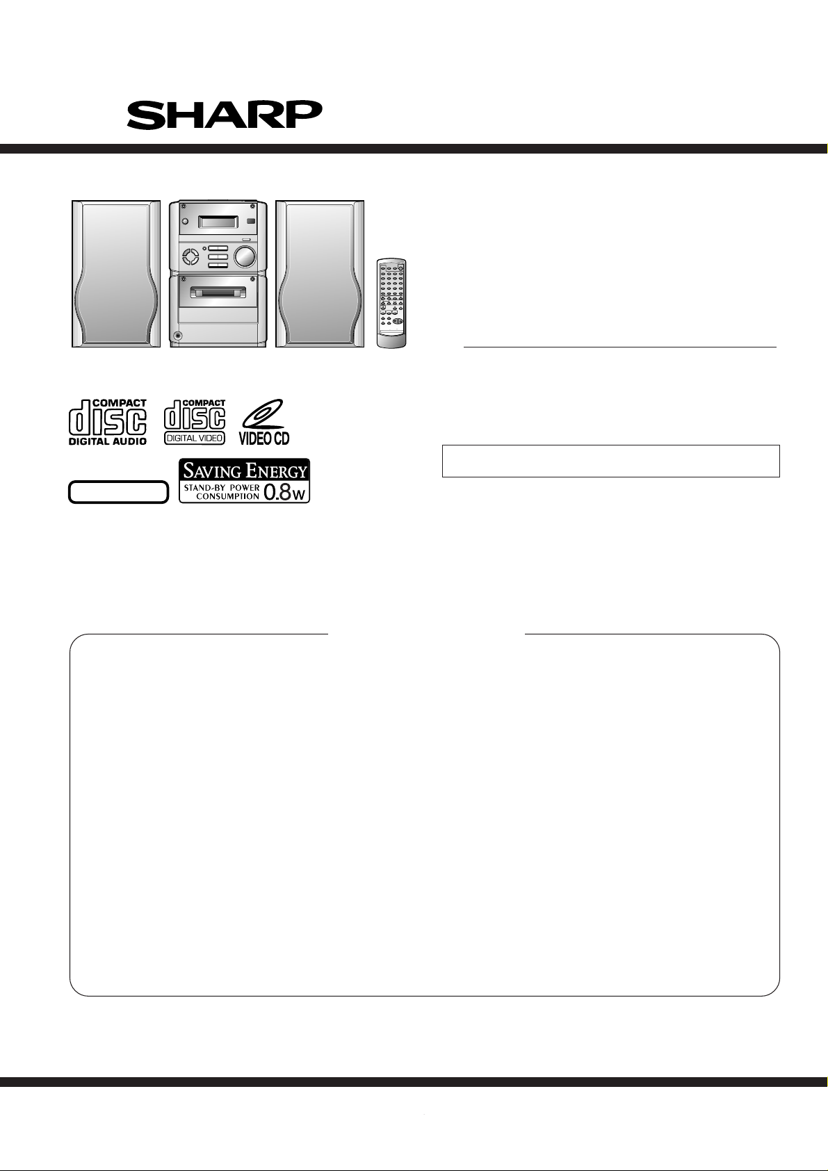
XL-30V
SERVICE MANUAL
No. S0081XL30V///
VIDEO CD MICRO SYSTEM
MODEL
XL-30V Video CD Micro System consisting of XL-30V (main unit)
and CP-XL30V (speaker system).
• In the interests of user-safety the set should be restored to its original
condition and only parts identical to those specified should be used.
NTSC/PAL
XL-30V
CONTENTS
Page
SAFETY PRECAUTION FOR SERVICE MANUAL .............................................................................................................2
VOLTAGE SELECTION.......................................................................................................................................................2
AC POWER SUPPLY CORD AND AC PLUG ADAPTOR ................................................................................................... 2
SPECIFICATIONS ...............................................................................................................................................................3
NAMES OF PARTS ............................................................................................................................................................. 4
OPERATION MANUAL ........................................................................................................................................................ 6
DISASSEMBLY................................................................................................................................................................... 8
REMOVING AND REINSTALLING THE MAIN PARTS.................................................................................................... 10
ADJUSTMENT .................................................................................................................................................................. 12
TEST MODE ..................................................................................................................................................................... 15
ERROR LIST..................................................................................................................................................................... 17
NOTES ON SCHEMATIC DIAGRAM ............................................................................................................................... 19
TYPES OF TRANSISTOR AND LED................................................................................................................................ 19
BLOCK DIAGRAM ............................................................................................................................................................ 20
SCHEMATIC DIAGRAM / WIRING SIDE OF P.W.BOARD.............................................................................................. 26
VOLTAGE ......................................................................................................................................................................... 40
WAVEFORMS OF CD CIRCUIT....................................................................................................................................... 41
TROUBLESHOOTING ...................................................................................................................................................... 42
FUNCTION TABLE OF IC................................................................................................................................................. 49
LCD SEGMENT ................................................................................................................................................................ 62
PARTS GUIDE/EXPLODED VIEW
SHARP CORPORATION
– 1 –
This document has been published to be used
for after sales service only.
The contents are subject to change without notice.
Page 2
XL-30V
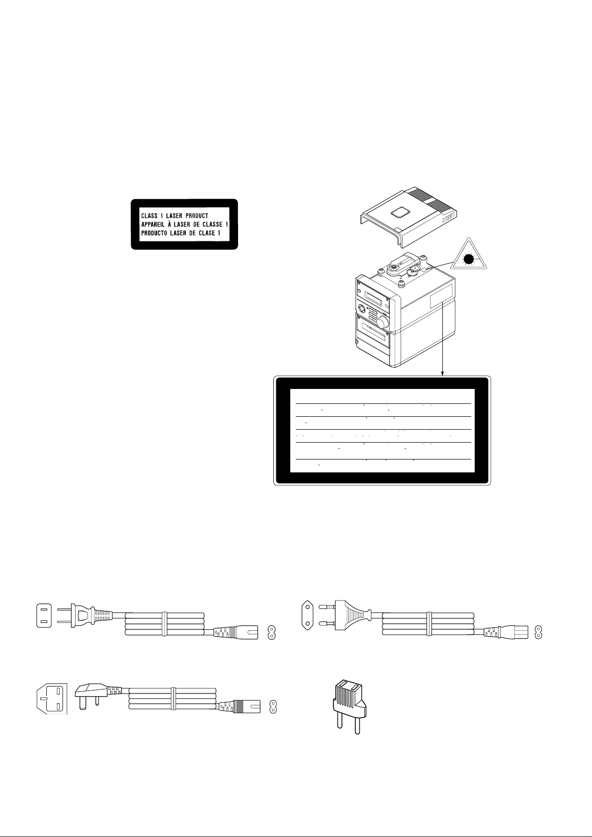
SAFETY PRECAUTION FOR SERVICE MANUAL
Precaution to be taken when replacing and servicing the Laser Pickup.
The AEL (Accessible Emission Level) of Laser Power Output for this model is specified to be lower than Class 1 Requirements.
However, the following precautions must be observed during servicing to protect your eyes against exposure to the Laser beam
(1) When the cabinet has been removed, the power is turned on without a compact disc, and the Pickup is on a position outer than
the lead-in position, the Laser will light for several seconds to detect a disc. Do not look into the Pickup Lens.
(2) The Laser Power Output of the Pickup inside the unit and replacement service parts have already been adjusted prior to shipping.
(3) No adjustment to the Laser Power should be attempted when replacing or servicing the Pickup.
(4) Under no circumstances look directly into the Pickup Lens at any time.
(5) CAUTION - Use of controls or adjustments, or performance of procedures other than those specified herein may result in
hazardous radiation exposure.
CAUTION
Laser Diode Properties
Material: GaAIAs
Wavelength: 780 nm
Emission Duration: continuous
Laser Output: max. 0.6 mW
● This Video CD Micro System is classified as
a CLASS 1 LASER product.
● The CLASS 1 LASER PRODUCT label is located on the rear cover.
● Use of controls or adjustments or performance of procedures other than those specified herein may result in hazardous radiation
exposure.
As the laser beam used in this compact disc
player is harmful to the eyes, do not attempt
to disassemble the cabinet. Refer servicing
to qualified personnel only.
CAUTION-INVISIBLE LASER RADIATION WHEN OPEN. DO NOT STARE INTO
BEAM OR VIEW DIRECTLY WITH OPTICAL INSTRUMENTS.
VARNING-OSYNLIG LASERSTRALNING NAR DENNA DEL AR OPPNAD. STIRRA
EJ IN I STRALEN OCH BETRAKTA EJ STRALEN MED OPTISKA INSTRUMENT.
ADVERSEL-USYNLIG LASERSTRALING VED ABNING. SE IKKE IND I
STRALEN-HELLER IKKE MED OPTISKE INSTRUMENTER.
VARO! AVATTAESSA OLET ALTTIINA NAKYMATON LASERSATEILYLLE.
ALA TUIJOTA SATEESEEN ALAKA KATSO SITA OPTISEN LAITTEEN LAPI.
VARNING-OSYNLIG LASERSTRALNING NAR DENNA DEL AR OPPNAD.
STIRRA EJ IN I STRALEN OCH BETRAKTA EJ STRALEN GENOM OPTISKT
INSTRUMENT.
ADVERSEL-USYNLIG LASERSTRALING NAR DEKSEL APNES. STIRR IKKE
INN I STRALEN ELLER SE DIREKTE MED OPTISKE INSTRUMENTER.
VOLTAGE SELECTION
Before operating the unit on mains, check the preset voltage. If the voltage is different from your local voltage, adjust the voltage
as follows, turn the selector with a screwdriver until the appropriate voltage number appears in the window (110V - 127 V or
220 V - 240 V AC).
AC POWER SUPPLY CORD AND AC PLUG ADAPTOR
QACCA0001SJ00
QACCE0001SJ00
QACCB0001SJ00 QPLGA0253AFZZ
– 2 –
Page 3

(
)
XL-30V
XL-30V
FOR A COMPLETE DESCRIPTION OF THE OPERATION OF THIS UNIT, PLEASE REFER
TO THE OPERATION MANUAL.
SPECIFICATIONS
● General
Power source:
Power consumption:
Dimensions:
Weight:
● Amplifier section
Output power:
Output terminals:
● Video CD section
Video output
format:
● Compact disc player section
Type: Compact disc player
Signal readout: Non-contact, 3-beam semi-
D/A converter: 1-bit D/A converter
Filter: 8-times oversampling digital
Frequency response:
Wow and flutter: Unmeasurable
AC 110 - 127/220 - 240 V,
50/60 Hz
35 W
Width; 160 mm (6-5/16")
Height; 241 mm (9-1/2")
Depth; 249 mm (9-13/16")
3.1 kg (6.8 lbs.)
MPO; 14 W (7 W + 7 W)
(10 % T.H.D.)
RMS; 10 W (5 W + 5 W)
(10 % T.H.D.)
Speakers; 4 ohms
Headphones; 16 - 50 ohms
(recommended; 32 ohms)
Video out: 1 Vp-p (75 ohms)
PAL / NTSC
conductor laser pickup
filter
20 - 20,000 Hz
less than 0.001% W. peak
● Tuner section
Frequency range:
● Cassette deck section
Frequency response: 50 - 14,000 Hz (Normal tape)
Signal/noise ratio: 50 dB
Wow and flutter: 0.25 % (WRMS)
CP-XL30V
Type: Full range speaker system
Speakers: 10 cm (4") full-range speaker
Rated input power:
Maximum input power:
Impedance: 4 ohms
Dimensions: Width; 145 mm (5-3/4")
Weight: 1.5 kg (3.3 lbs.)/each
Specifications for this model are subject to change without
prior notice.
FM; 88-108 MHz
AM; 531-1,602 kHz
5 W
10 W
Height; 240 mm (9-1/2")
Depth; 191 mm (7-9/16")
– 3 –
Page 4
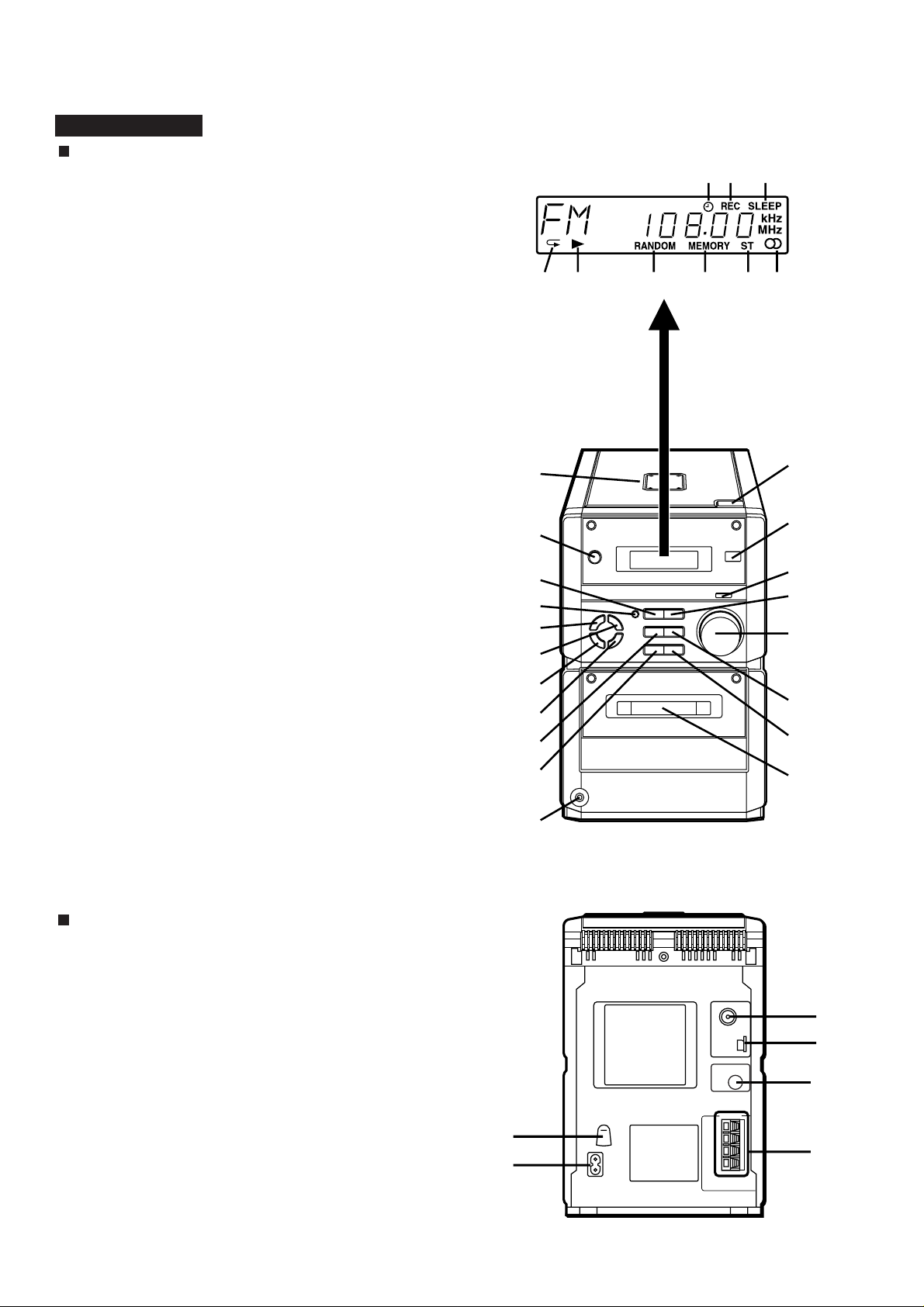
XL-30V
XL-30V
Front panel
1. Timer Indicator
2. Record Indicator
3. Sleep Indicator
4. (VCD/CD) Repeat Indicator
5. (VCD/CD) Play Indicator
6. (VCD/CD) Random Indicator
7. (VCD/CD/TUNER) Memory Indicator
8. FM Stereo Mode Indicator
9. FM Stereo Indicator
10. VCD/CD Compartment
11. On/Stand-by Button
12. (VCD) Stop/Return Button
(CD/TAPE) Stop Button
(TUNER) Memory Clear Button
13. (TAPE) Record Pause Button
14. Bass/Treble Selector Button
15. Memory/Set Button
16. Clock/Timer/Sleep Button
17. Band Selector Button
18. (VCD) Skip/Previous Button
(CD) Track Down Button
(TAPE) Rewind Button
(TUNER) Tuning Down Button
19. Function Selector Button
20. Headphones Socket
21. (VCD/CD) Eject Button
22. Remote Control Sensor
23. Volume Select Button
24. (VCD/CD/TAPE) Play Button
25. Volume/Jog Dial
26. (VCD) Skip/Next Button
(CD) Track Up Button
(TAPE) Fast Forward Button
(TUNER) Tuning Up Button
27. Volume/Jog Dial Selector Button
28. Cassette Compartment
NAMES OF PARTS
10
11
12
13
14
15
16
17
18
19
20
1
5
4
6
7
3
2
9
8
21
22
23
24
25
26
27
28
Rear panel
1. Voltage Selector
2. AC Power Input Socket
3. FM 75 ohms Aerial Socket
4. AM Loop Aerial Socket
5. Video Output Socket
5.
6. Speaker Terminals
3
4
5
1
6
2
– 4 –
Page 5
XL-30V
Remote control
1. Remote Control Transmitter LED
2. Timer Button
3. (VCD/CD) Audio Mode Button
4. (VCD/CD) Direct Search Buttons
5. (VCD/CD) Display Button
6. (VCD) Video Intro Button
7. Sleep Button
8. On/Stand-by Button
9. (VCD) TV Type Button
10. (VCD) Track Digest Button
11. (VCD) Time Search Button
12. (VCD/CD) Memory Button
13. (VCD/CD) Clear Button
14. (VCD/CD) Random Button
15. (VCD) Playback Control Auto/Off Button
16. (VCD) Skip/Previous Button
(CD) Track Down Button
17. (VCD) Skip/Next Button
(CD) Track Up Button
18. (VCD/CD) Repeat Button
19. (VCD/CD) Pause Button
20. (VCD/CD) Review Button
(TAPE) Rewind Button
21. (VCD/CD) Cue Button
(TAPE) Fast Forward Button
22. (VCD) Stop/Return Button
(CD/TAPE) Stop Button
23. (VCD/CD/TAPE) Play Button
24. (TAPE) Record Pause Button
25. Function Buttons
26. Treble Buttons
27. Bass Buttons
28. (TUNER) Preset Up/Down Buttons
29. Volume Up/Down Buttons
24
25
26
27
XL-30V
1
2
3
7
8
4
9
5
6
12
13
14 15
10
11
16 17 1918
20 21
22 23
28
29
CP-XL30V
1. Bass Reflex Duct
2. Full-Range Speaker
3. Speaker Wire
1
2
3
– 5 –
Page 6
XL-30V
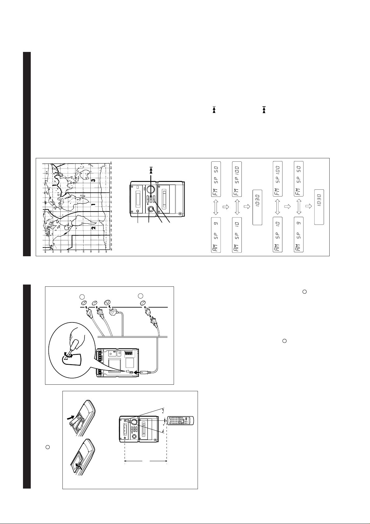
■ AM/FM interval (span)
The International Telecommunication Union (ITU)
has established that member countries should
maintain either a 10 kHz or a 9 kHz interval be-
tween broadcasting frequencies of any AM station.
The illustration shows the 9 kHz interval zones (re-
gions 1 and 3), and the 10 kHz interval zone (re-
gion 2).
This product is not equipped with a span selector.
OPERATION MANUAL
Press the ON/STAND-BY button to turn the
power on.2Press the FUNCTION button until “FM” or
“AM” appears in the display.3Press the BAND button to select the AM
band.
radio has been adjusted for a 9 kHz span. If “AM
530 kHz” is displayed, it means that the radio
has been adjusted for a 10 kHz span.
However, it will be adjusted to 9 kHz AM inter val
(50 kHz FM interval) when shipped from the fac-
tory.
Before using the unit, be sure to set it for the AM
tuning interval (span) used in your area.
To check the tuning span currently selected:
1
● If “AM 531 kHz” is displayed, it means that the
T o change from a 9 kHz AM (50 kHz FM) interval
to a 10 kHz AM (100 kHz FM) interval:
Press the ON/STAND-BY b utton to enter the
stand-by mode.2Hold down the button and the MEMORY/
SET button for at least 4 seconds. Release
1
the buttons when “AM SP 10 kHz” and “FM
SP 100 kHz” are displayed alternately.
● The unit will return to the clock display.
Press the ON/STAND-BY b utton to enter the
To return to a 9 kHz AM (50 kHz FM) interval:
1
stand-by mode.2Hold down the button and the MEMORY/
SET button for at least 4 seconds. Release
the buttons when “AM SP 9 kHz” and “FM
SP 50 kHz” are displayed alternately.
● The unit will return to the clock display.
span has been switched and AC power lead dis-
connected, it will be automatically returned to a
Caution:
● When the unit is left for a few hours after the
9 kHz span. If this happens, set the span again.
memorised will be cancelled.
● When the span is switched, any stations that are
kHz
kHz
BAND
SET
MEMORY/
ON/
STAND-BY
1
2
FUNCTION
kHz kHz
kHz
kHz
kHz kHz
).
1
To an AC socket
is used, connect the unit
2
220Vı240V
RATED
LINE VOL TAGE
■ Connecting the AC power lead
-
unit to malfunction.
■ Remote control
them towards the battery terminals.
● When inserting or removing the batteries, push
● Installing the batteries incorrectly may cause the
PREPARATION FOR USE PREPARATION FOR USE
or similar)
● 2 “AA” size batteries (UM/SUM-3, R6, HP-7
0.2m - 6m
(8"- 20')
the unit is not to be used for a prolonged period
of time.
plied.
Otherwise, a malfunction or an accident may
Check the setting of the AC voltage selector located
on the rear panel before plugging the unit into an
AC socket. If necessary, adjust the selector to cor-
respond to the AC power voltage used in your area.
Selector adjustment:
Turn the selector with a screwdriver until the ap-
propriate voltage number appears in the window
(110V - 127V or 220V - 240V AC).
Notes:
● Unplug the AC power lead from the AC socket if
15
15
dicated in the battery compartment.
same time.
unit will not be used for long periods of time. This
will prevent potential damage due to battery leak-
Precautions for battery use:
● Insert the batteries according to the direction in-
● Replace all old batteries with new ones at the
● Do not mix old and new batteries.
● Remove the batteries if they are weak or if the
age.
occur.
● Never use a power lead other than the one sup-
Caution:
Do not use rechargeable batteries (nickel-cadmium
battery, etc.).
using the AC plug adaptor supplied with the unit,
● AC Plug Adaptor
Notes concerning use:
as illustrated. The AC plug adaptor is not included
In areas (or countries) where an AC socket as
shown in illustration
reduced or if the operation becomes erratic.
mote control and the sensor on the main unit
● Replace the batteries if the operating distance is
● Periodically clean the transmitter LED on the re-
Note for users in Australia and New Zealand:
An AC plug adaptor is not supplied if the lead has
in areas where the AC wall socket and AC power
plug can be directly connected (see illustration
with a soft cloth.
● Exposing the sensor on the main unit to strong
an Australian Standard plug.
light may interfere with operation. Change the
lighting or the direction of the unit.
excessive heat, shock, and vibrations.
● Keep the remote control away from moisture,
– 6 –
Page 7
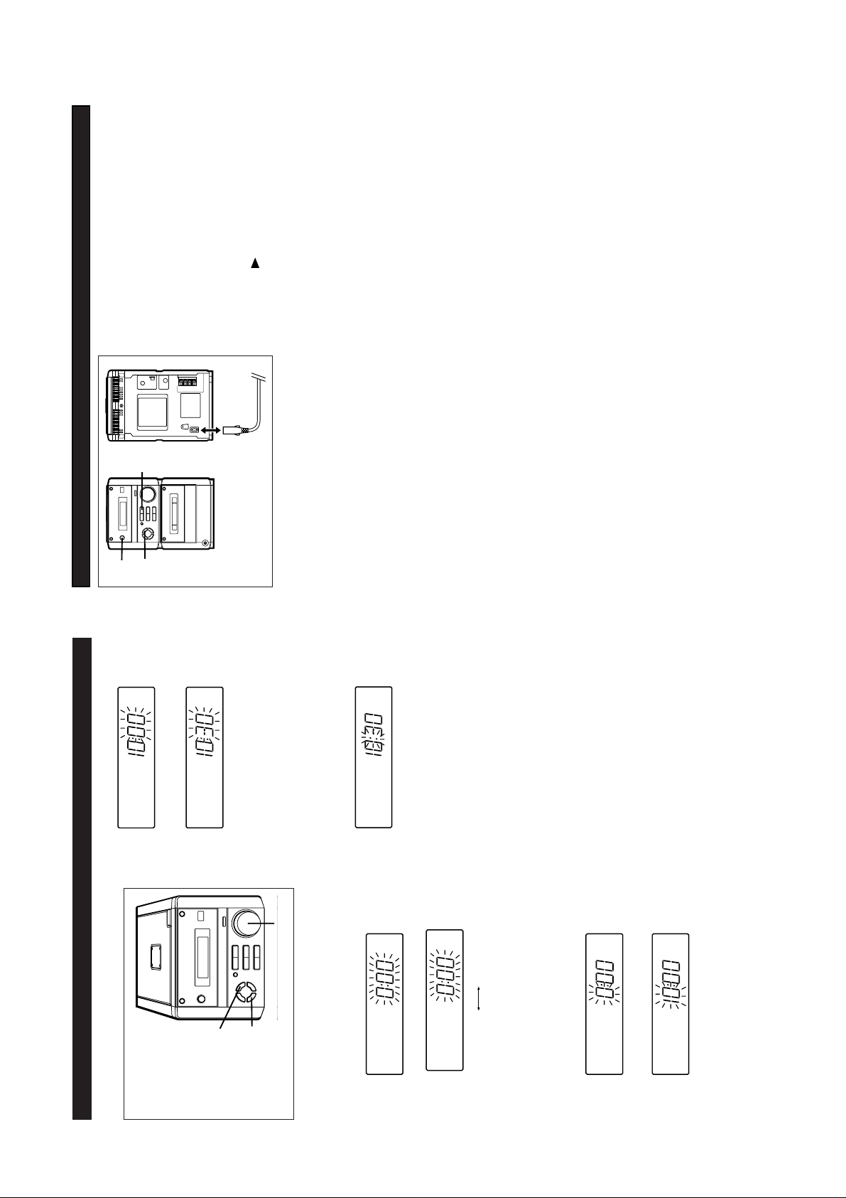
Press the ON/ST AND-BY button to enter the
stand-by mode.
Unplug the AC power lead from the AC IN-
PUT socket on this unit.
Whilst pressing down the MEMORY/SET but-
ton and the button, plug the AC power lead
and timer settings, and tuner and CD presets).
Reset the microcomputer under the following
conditions:
● To erase all of the stored memory contents (clock
● If the display is not correct.
● If the operation is not correct.
1
2
AC INPUT
into the AC INPUT socket on this unit.
3
stored in memory, such as clock and timer set-
Caution:
● The operation explained above will erase all data
2,3
3
XL-30V
tings, and tuner and CD presets.
3
1
RESETTING THE MICROCOMPUTER
the time will increase by 1 minute. When it is
turned one click anti-clockwise, the time will de-
crease by 1 minute.
Keep turning the jog dial to change the time con-
tinuously.
Press the MEMORY/SET button.
6
Adjust the minutes by turning the jog dial.
7
● When the jog dial is turned one click clockwise,
utes advance from “59” to “00”.
● The hour setting will not advance even if min-
Jog dial
Press the MEMORY/SET button.
8
(Seconds are not displayed.)
● The clock starts operating from “0” seconds.
AC power supply is restored after a power fail-
ure occurs or after the AC power lead is discon-
nected.
If this happens, follow the procedure below to
Note:
● The clock display will flash on and off when the
change the clock time.
T o change the clock time:
Perform steps 1, 2 and 5 - 8 above.
THE MICROCOMPUTER”.
To change the time display mode:
➀Perform steps 1 - 3 in the section “RESETTING
➁Perform steps 1 - 8 above.
CLOCK/TIMER/
SLEEP
SETTING THE CLOCK
In this example, the clock is set for the 24-hour
(0:00) system.
MEMORY/SET
Press the CLOCK/TIMER/SLEEP button.2Within 3 seconds, press the MEMORY/SET
button.3Turn the jog dial to select the time display mode.
(Main unit operation)
1
– 7 –
0:00 AM 12:00
(0:00 - 23:59)
“0:00” → The 24-hour display will appear.
(AM 12:00 - PM 11:59)
first installed or it has been reset.
Press the MEMORY/SET button.5Adjust the hour by turning the jog dial.
● Note that this can only be set when the unit is
“AM 12:00” → The 12-hour display will appear.
4
● When the jog dial is turned one click clockwise,
the time will increase by 1 hour. When it is turned
one click anti-clockwise, the time will decrease
by 1 hour.
Keep turning the jog dial to change the time con-
tinuously.
change automatically to “PM”.
● When the 12-hour display is selected, “AM” will
Page 8
XL-30V
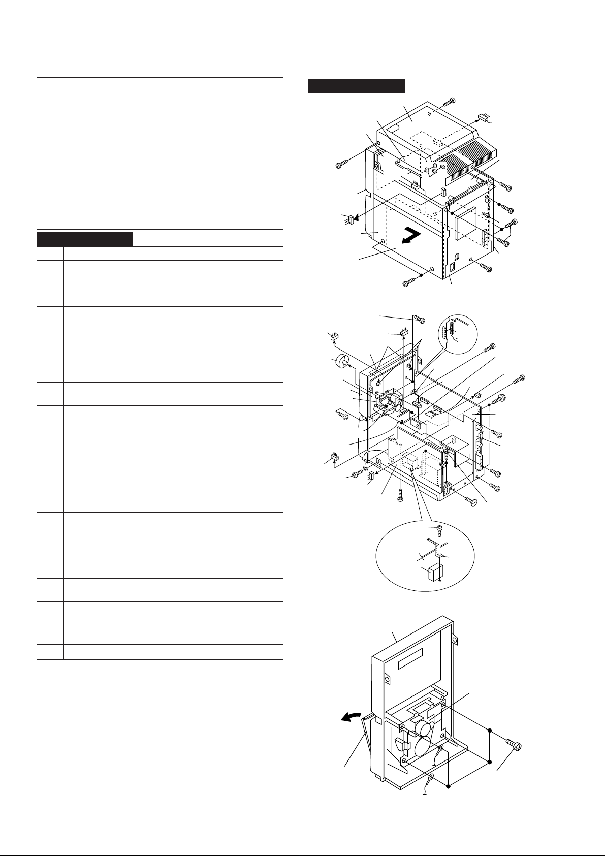
DISASSEMBLY
Follow the below-mentioned notes when disassembling
the unit and reassembling it, to keep it safe and ensure
excellent performance:
1. Take cassette tape and compact disc out of the unit.
2. Be sure to remove the power supply plug from the wall
outlet before starting to disassemble the unit.
3. Take off nylon bands or wire holders where they need to
be removed when disassembling the unit. After servicing
the unit, be sure to rearrange the leads where they were
before disassembling.
4. Take sufficient care on static electricity of integrated
circuits and other circuits when servicing.
XL-30V
STEP REMOVAL
1 Side Panel 1. Screw ................. (A1) x8 8-1
(Left/Right)
2 Top Cabinet 1. Screw ................. (B1) x1 8-1
3 Rear Panel 1. Screw ................. (C1) x3 8-1
4 Main PWB/ 1. Screw ................. (D1) x2 8-2
Headphones PWB 2. Screw ................. (D2) x3
5 Jog Switch PWB 1. Socket ................ (E1) x1 8-2
6 Display PWB/ 1. Screw ................. (F1) x3 8-2
LED PWB 2. Screw ................. (F2) x3
(With Jog Motor 3. Bracket ............... (F3) x1
Holder) 4. Socket ................ (F4) x1
7 Front Panel 1. Screw ................. (G1) x1 8-2
8 Power PWB 1. Screw ................. (H1) x4 8-2
9 Tape Mechanism 1. Open the cassette holder. 8-3
10 Video PWB 1. Screw ................. (K1) x4 8-4
11 CD PWB/ 1. Screw ................. (L1) x4 8-4
Open Close Switch 2. Bracket............... (L2) x3
PWB (Note) 3. Hook ................... (L3) x2
12 CD Mechanism 1. Screw ................. (M1) x3 8-5
Note:
After removing the connector for the optical pickup from the
connector, wrap the conductive aluminium foil around the
front end of connector remove to protect the optical pickup
from electrostatic damage.
PROCEDURE
2. Socket ................ (B2) x5
3. Bracket ............... (D3) x1
4. Socket ................ (D4) x3
5. Flat wire.............. (D5) x1
6. Socket ................ (D6) x1
2. Screw ................. (E2) x2
3. Knob ................... (F5) x1
6. Hook ................... (F6) x2
7. Hook ................... (F7) x2
2. Socket ................ (G2) x1
3. Screw ................. (G3) x1
2. Screw ................. (H2) x1
3. Screw ................. (H3) x1
4. Bracket ............... (H4) x1
2. Screw ................. (J1) x4
2. Socket ................ (K2) x3
4. Socket ................ (L4) x3
FIGURE
(A1)x1
ø3x10mm
Front
Panel
(B2)x1
Side Panel
(Right)
Power
PWB
(E1)x1
(F5)x1
Display PWB
Front Panel
Jog Switch
PWB
(E2)x2
ø2.5x12mm
Jog Motor
Tape
Holder
Mechanism
PWB
(F4)x1
(G3)x1
ø3x6mm
Open
XL-30VCaution on Disassembly
Top Cabinet
CD PWB
Display
PWB
(A1)x2
ø3x10mm
(F2)x2
ø2.5x10mm
(D4)x1
LED
(F7)x2
PWB
(D4)x1
Power PWB
Front Panel
(B2)x1
Figure 8-1
(G1)x1
ø3x8mm
(H3)x1
ø3x6mm
Power PWB
Sub Power
Transformer
Figure 8-2
(B2)x2
(F6)x2
(A1)x1
ø3x10mm
Rear Panel
(D6)x1
(F3)x1
(D4)x1
(H2)x1
ø3x10mm
(H4)x1
(B2)x1
Main PWB
(B1)x1
ø3x10mm
Side Panel
(Left)
(C1)x1
ø3x10mm
(D2)x1
ø3x8mm
Headphones
PWB
(G2)x1
(D5)x1
(D1)x2
ø3x10mm
Main PWB
(F2)x1
ø2.5x10mm
(D3)x1
(F1)x3
ø2.5x14mm
(D2)x1
ø3x8mm
(H1)x4
ø3x6mm
Tape
Mechanism
(C1)x2
ø3x10mm
(A1)x4
ø3x10mm
(D2)x1
ø3x8mm
– 8 –
Cassette
Holder
(J1)x4
ø2.5x10mm
Figure 8-3
Page 9
XL-30V
(K1)x4
ø2x10mm
Video PWB
(L1)x4
ø2.5x14mm
(L2)x1
CD PWB
(L4)x1
(L3)x2
Open/Close
Switch PWB
CD Motor PWB
(K2)x1
(K2)x2
(L2)x1
(L2)x1
Top Cabinet
CD Mechanism
(L4)x2
CD Mechanism
(M1)x3
ø2.5x10mm
PWB Washer x3
Top Cabinet
Figure 9-1 Figure 9-2
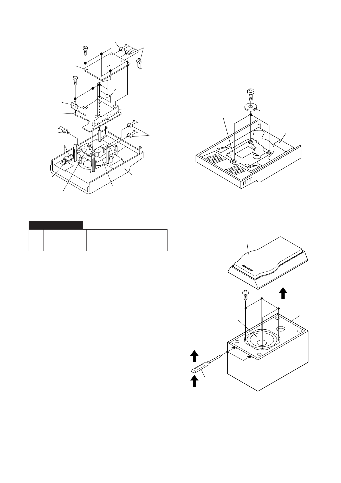
CP-XL30V
STEP REMOVAL PROCEDURE FIGURE
1 Woofer 1. Front panel .......... (A1) x1 9-3
2. Screw .................. (A2) x4
(A1)x1
(A2)x4
ø4x12mm
Speaker Box
Woofer
Direction of handle
Driver should be
pried away from
speaker Box.
– 9 –
Screwdriver
Figure 9-3
Page 10
XL-30V
REMOVING AND REINSTALLING THE MAIN PARTS
TAPE MECHANISM SECTION
Perform steps 1 to 7 and 9 of the disassembly method to
remove the tape mechanism. (See page 8.)
How to remove the record / playback and erase
heads (See Fig. 10-1.)
1. Remove the screws (A1) x 2 pcs., to remove the erase head.
2. Remove the screws (A2) x 2 pcs., to remove the record/
playback head.
Note:
After replacing the heads and performing the azimuth
adjustment, be sure to apply screw lock.
How to remove the pinch roller (See Fig. 10-2.)
1. Carefully bend the pinch roller pawl in the direction of the
arrow <A>, and remove the pinch roller (B1) x 1 pc.,
upwards.
(A2)x1
ø2x7mm
(A1)x2
ø2x8mm
Erase Head
Record/
Playback Head
Pinch Roller
(B1)x1
(A2)x1
ø2x3mm
Figure 10-1
<A>
Pinch Roller
Pawl
Figure 10-2
How to remove the belts (See Fig. 10-3.)
1. Remove the main belt (C1) x 1 pc., from the motor pulley.
2. Remove the FF/REW belt (C2) x 1 pc., from the REW/FF
clutch.
3. Put on the belts in the reverse order of removal.
Note:
When putting on the belt, ascertain that the belt is not twisted,
and clean it.
How to remove the motor (See Fig. 10-4.)
1. Remove the main belt.
2. Remove the screws (D1) x 2 pcs., to remove the motor
bracket.
3. Remove the screws (D2) x 3 pcs., to remove the motor.
Note:
When mounting the motor, pay attention to the motor mounting
angle.
Main Belt
(C1)x1
(D1)x1
ø2x4mm
Motor
REW/FF
Clutch
FF/REW Belt
(C2)x1
Figure 10-3
(D2)x3
Special
Screw
Motor
Motor
Bracket
– 10 –
(D1)x1
ø2x4mm
Motor
Figure 10-4
Page 11
XL-30V
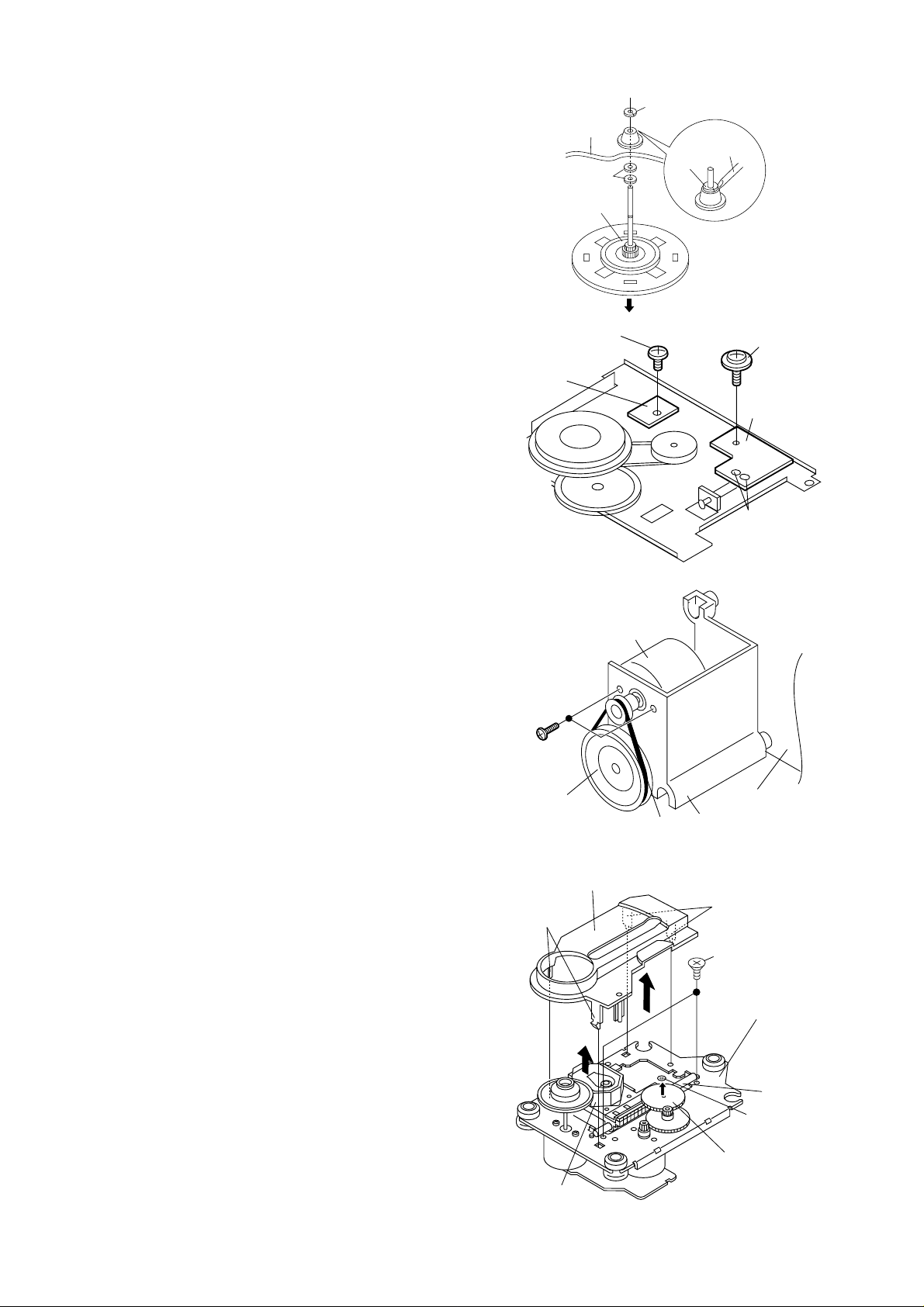
How to remove the flywheel (See Fig. 11-1.)
1. Remove the belt.
2. Remove the stop washer (E1) x 1 pc., with a small precision
screwdriver to extract the flywheel from the capstan metal.
Note:
When the stop washer is deformed or damaged, replace it with
a new one.
How to reinstall the parts
Install each part in the reverse order of the removal with care.
How to remove the tape mechanism PWB
(See Fig. 11-2.)
1. Remove the screw (F1) x 1 pc., to remove the tape
mechanism PWB.
2. Remove the screw (F2) x 1 pc.
3. Remove the solder joints (F3) x 2 pcs., to remove the tape
mechanism PWB.
Mechanism
Chassis
Washer x 2
Flywheel
(F1)x1
Tape
ø2x3mm
Mechanism
PWB
(E1)x1
Stop Washer
Stop
Washer
Figure 11-1
Driver
(F2)x1
ø2x8mm
Tape
Mechanism
PWB
(F3)x2
Solder
Joint
How to remove the jog motor (See Fig. 11-3.)
1. Remove the side panel and top cabinet.
2. Remove the jog belt (G1) x 1 pc., from the motor pulley.
3. Remove the screws (G2) x 2 pcs., to remove the jog motor.
Note:
When putting on the belt, ascertain that the belt is not twisted,
and clean it.
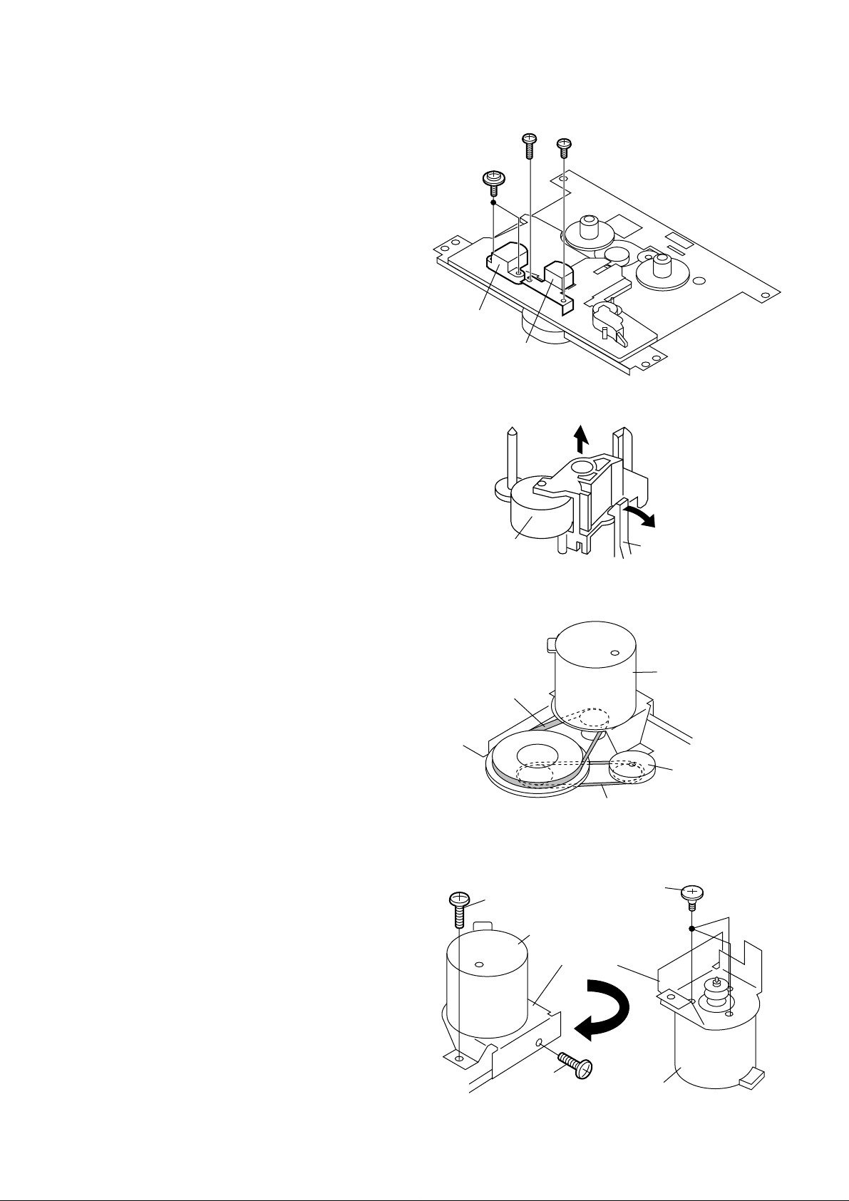
CD MECHANISM SECTION
Perform steps 1, 2, 10, 11 and 12 of the disassembly method
to remove the CD mechanism.
How to remove the pickup (See Fig. 11-4.)
1. Remove the mechanism cover, paying attention to the
pawls (A1) x 4 pcs.
2. Remove the screws (A2) x 2 pcs., to remove the shaft
(A3) x 1 pc.
3. Remove the stop washer (A4) x 1 pc., to remove the gear
(A5) x 1 pc.
4. Remove the pickup.
Note:
After removing the connector for the optical pickup from the
connector, wrap the conductive aluminium foil around the
front end of connector remove to protect the optical pickup
from electrostatic damage.
(G2)x2
ø2x5mm
Worm
Gear
(A1) x2
Pickup Unit
Figure 11-2
Jog Motor
Jog Belt
(G1)x1
Figure 11-3
Mechanism Cover
Figure 11-4
Display PWB
Jog Motor
Holder
(A1) x2
(A2) x2
ø2.6 x6mm
CD Mechanism
Shaft
(A3) x1
Stop Washer
(A4) x1
Gear
(A5) x1
– 11 –
Page 12
XL-30V
ADJUSTMENT
CD SECTION
Since this CD system incorporates the following automatic
adjustment function, when the pickup is replaced, it is not
necessary to readjust it.
VIDEO CD SECTION
A-BEX
TEST VIDEO CD
Model No.
• Measurement of oscillation frequency
Disc Adjusting
Point
CD Stop TC100V 27.00000 MHz1 of R163V and
Instrument
Connection
± 160 Hz
• Checking of video output signal
Checking of color bar
Disc
Track 2 Video output terminal Chroma Peak Level
Adjusting Point
TVD-581
TVD-581A
Specified Value
2
of C183V
Instrument
Connection
100 ± 15 IRE
SET
Video Output Terminal
Video Input Terminal
TV
Figure 12-3 Checking of video output signal
VIDEO PWB
R163V
1
TC100V
PCLK2X
C183V
2
GND
IC15V
Figure 12-1 ADJUSTMENT POINTS
SET
VIideo Output Terminal
XL100V
IC14V
140 IRE
40 IRE
(1V)
(0.286V)
40 IRE
Color Burst
100 IRE
(0.714V)
-40
Gray
100 100
75
33.5
20
-20
Gray
Figure 12-4
Cyan
Yellow
(59.94Hz/NTSC)
IH
88.5
5
0
-13.5
Magenta
Cyan
Yellow
Green
75
Green
Magenta
Color bar signal
70
waveform
41.5
-25 -25
Blue
Red
Red
Blue
Horizontal
sync signal
75 ohms
GND
Vectorscope
Waveform monitor
or oscilloscope
Figure 12-2 Measurement of oscillation frequency
TV monitor
Figure 12-5
– 12 –
Page 13
Checking of vector scope waveform
Checking SettingDisc Checking
Item
Track 2 VIDEO OUT Set the phase of Phase check
color burst signal ± 10°
(B) to 180°-360°
line.
( Check that the setting is within the illustrated range.)
XL-30V
I
R-Y
R
MG
YL
75%
-Q
G
CY
-I
[NTSC] [PAL]
Checking the black-and-white level
Checking Checking ItemDisc
Track 16 VIDEO OUT Output level
100 ± 10 IRE
100% Luminance
B
Q
B-Y
Figure 13-1
YL
yl
G
g
75%
R
V
cy
CY
MG
b
U
B
mg
100IRE
40IRE
Horizontal Interval
reference signal
40IRE
100% WHITE LEVEL
Figure 13-2
– 13 –
Page 14
XL-30V
MECHANISM SECTION
• Driving Force Check
Torque Meter
Play: TW-2412 Over 80 g
Specified Value
• Torque Check
Torque Meter
Play: TW-2111 30 to 60 g.cm
Fast forward: TW-2231 55 to 140 g.cm
Rewind: TW-2231 55 to 140 g.cm
Specified Value
• Tape Speed
Test Tape
MTT-111 Variable 3,000 ± 90 Hz Headphones
Adjusting
Point
resistor in jack
motor. (M901)
Specified
Value
Instrument
Connection
TAPE MECHANISM
M901
Tape
Motor
Variable
resistor
in motor
Figure 14-1 ADJUSTMENT POINT
TUNER SECTION
fL: Low-range frequency
fH: High-range frequency
• AM IF/RF
Signal generator: 400 Hz, 30%, AM modulated
Test Stage
AM IF 450 kHz 1,602 kHz T351 *1
AM Band — 531 kHz (fL): T306 *2
Coverage 1.1 ± 0.1 V
AM Tracking 990 kHz 990 kHz T302 *1
*1. Input: Antenna Output: Speaker Terminal
*2. Input: Input is not connected Output: TP301
• FM Mute Level
Signal generator: 1 kHz, 40 kHz dev., FM modulated
Frequency
98.00 MHz 98.00 MHz VR351 *1 Input: SO301
(25 dBµV) Output: Speaker
*1. Adjust so that an output signal appears.
Frequency Frequency
Display
Display
Adjusting
Parts
Setting/
Adjusting
Parts
Connection
Terminal
Instrument
Connection
Instrument
• FM Detection
Signal generator: 10.7 MHz, FM sweep generator
Frequency
Test
Stage
FM IF 10.7 MHz 98.00 MHz T304 (Turn Input: Pin 1 of
Frequency
Display
Setting/
Adjusting
Parts
the core of IC301
T304 fully
counterclockwise).
Instrument
Connection
• FM RF
Signal generator: 1 kHz, 75 kHz dev., FM modulated
Test Stage
FM Band — 87.50 MHz (fL): L303 *1
Coverage 3.4 ± 0.1 V
FM RF 98.00 MHz 98.00 MHz L302 *2
Frequency
(10~30 dB)
Frequency
Display
Setting/
Adjusting
Parts
Instrument
Connection
*1. Input: Antenna Output: TP301
*2. Input: Antenna Output: Speaker Terminal
• Setting the Test Mode
Keeping the FF/FWD button and MEMORY button pressed,
turn on POWER. Then, the frequency is initially set in the
memory as shown in Table. Call it with the Jog volume button
by pressing the VOLUME/JOG button to use it for adjustment
and check of tuner circuit.
Preset No.
1 87.50 MHz 6 531 kHz
2 108.00 MHz 7 1,602 kHz
3 98.00 MHz 8 990 kHz
4 90.00 MHz 9 603 kHz
5 106.00 MHz 10 1,404 kHz
Preset No. BAND
11~25
FM STEREO
Preset No.
Preset No. FM MONO
26 106.00 MHz
27 90.00 MHz
28 98.00 MHz
29 108.00 MHz
30 87.50 MHz
AM
MAIN PWB
SO301
FM ANTENNA
R336
FM Band
Coverage fL
FM IF
L302
L303
T304
FM RF
T302
9
IC301
1
AM
Tracking
CNP301
AM ANTENNA
T351
AM IF
AM Band
Coverage fL
FM Mute
Level
VR351
TP301
T306
– 14 –
Figure 14-2 ADJUSTMENT POINTS
Page 15
XL-30V
TEST MODE
The test mode applied to this microcomputer has three modes, namely ordinary test mode to be used for adjustment or
measurement, aging test mode to be used for aging test, and self-diagnosis test mode for self-inspection in case of final product
inspection.
1. Turning on the test mode
To turn on the specific test mode, press the POWER button, holding down the following two buttons in the ordinary stand-by
mode (power off state). In this case only the main unit button is valid. Even when the POWER of remote control button is set
to on, the test mode is not turned on.
[Ordinary test mode]
1. Tuner Test Mode (TEST 2)............................. Volume/JOG Dial Selector + Volume Select
2. Electronic volume Test Mode (TEST 3) ......... REW/REV + FF/FWD
3. Timer Test Mode (TEST 4) .............................FUNCTION + Volume Select
4. LCD Test Mode (TEST 5) ...............................FUNCTION + FF/FWD
[Self-diagnosis Test Mode]
1. Button input diagnosis test mode (TEST6)..... REW/REV + Volume Select
2. Tuner Test Mode (TEST 2)
1. Outline of tuner (radio) test mode
The tuner test mode is intended to store the adjustment and measurement frequencies in the preset memory CH without
frequency setting by adjusting personnel when the tuner section is adjusted in the production line.
2. Details of tuner test mode
When the power is turned on by using the "POWER" button while the "Volume/JOG Dial Selector" and "Volume Select"
buttons are held down in POWER OFF state, the frequency for adjustment and measurement of destination specified by the
AREA terminal is preset and stored in the preset memory CH. However, Ordinary 1 and Ordinary 2 are set to the designation
(destination selected by SPAN switching operation) set when the test mode is set. (As for frequencies to be preset and stored
for each destination, refer to item 3.)
The tuner test mode is started from preset No.1.
The operations of test mode are identical with the ordinary operations of TUNER function. However, FUNCTION switching
is invalid.
Since it is necessary to discard the content of preset memory when the tuner test mode is ended, "0000" or "1111" bits are
written in the memory to be checked in case of memory check (in case of initial setting) so that memory abnormality is detected
in case of initial setting so as to ensure memory initialization.
When the tuner test mode is turned on, the following indication lights for one second.
• The TUNER TEST2 mode is set as a result of Volume Select + POWER. -> IF AC is set to OFF in the TEST2 mode, the initial
state is restored.
When POWER is set to OFF, the memory of TEST2 mode is protected.
When the power is turned on again, the ordinary operation is enabled while the data is stored in the
memory (besides TUNER).
If AC OFF state is maintained in this state for about 1/2 day, start is executed in the initial state.
• To clear the whole memory, insert the AC cord, holding down MEMORY + PLAY.
– 15 –
Page 16
XL-30V
3. Preset frequencies for various destinations (random preset memory)
Ordinary 1,ChinaCH
1 FM 87.50 MHz
2 FM108.00 MHz
3 FM STEREO FM 98.00 MHz
4 FM 90.00 MHz
5 FM106.00 MHz
6 AM 531 kHz
7 AM1602 kHz
8 AM AM 990 kHz
9 AM 603 kHz
10 AM1404 kHz
11-15 LW
• The hatched sections of the table are not stored in memory.
16-20
21-25
26 FM106.00 MHz
27 FM 90.00 MHz
28 FM MONO FM 98.00 MHz
29 FM108.00 MHz
30 FM 87.50 MHz
BAND
Ordinary 1,ChinaCHBAND
3. Electronic volume Test Mode (TEST 3)
When the test mode is set, the following indication lights for one second.
When this mode is set, BASS/TREBLE is set to 0 (0 dB) and SURROUND mode is set to off, and start-up function is set to CD
when volume is -14 dB (STEP 17). The button operations in the test mode are the same as those of ordinary operation excepting
sound volume UP/DOWN.
(1) The indication is the same as that of ordinary operation excepting test mode setting.
(2) The sound volume control with the sound volume UP/DOWN button is only the following 3 steps unlike the ordinary state.
Volume- ∞ (STEP 0) <-> Volume-14 dB (STEP 23) <-> Volume-0 (STEP 30)
(3) BASS/TREBLE and SURROUND are switched when button operation is performed.
4. Timer test Mode (TEST 4)
When the test mode is set, the following indication lights for one second.
The current time and timer time are set in the following procedure to perform the timer playback.
1. Set the current time to 1:00, set the timer to ON time 1:02, set the function to Tape, and set volume STEP 8. One minute is
counted as one second, and the timer playback operation is performed. The fade-in (when playback is started) is executed
at a rate of one step for 0.5 sec. After completion of fade-in the fade-out is executed at a rate of one step for 0.5 sec (WAIT
1 sec inserted).
After completion of fade-out the power is turned off (after WAIT 1 sec), and the mode is changed to the stand-by mode.
The indication during operation is the same as that of ordinary timer operation.
5. LCD Test Mode (TEST 5)
When the LCD test mode is set, all the LCD segments are lighted. After that the indication is changed as follows according to
the "PLAY" button input.
Lighting of all segments Lighting of odd segments Lighting of even segments
– 16 –
Page 17
XL-30V
6. Key input diagnosis Test Mode (TEST 6)
When the test mode is set, the following indication appears.
This test mode is intended to check whether all the main unit buttons can be detected. Accordingly, in this test mode checking
as to whether the "POWER" button was pressed after all the buttons shown below were pressed is performed. If the result is
OK, OK is indicated. Even any one of keys was not pressed, an error is indicated. In case of OK termination or error termination
exit from this mode occurs when the "POWER" button is pressed next time, and the stand-by mode is set.
1. In case of "FF/FWD" + "REC PAUSE"
Since SURROUND and RDS are not provided, the following 11 buttons are detected as all buttons.
PLAY, JOG MODE, BAND, BASS/TREBLE, FUNCTION, MEMORY/SET, REC PAUSE, REW, FF, STOP, CLOCK/TIMER/
SLEEP.
The OK/NG indication of test result is as follows.
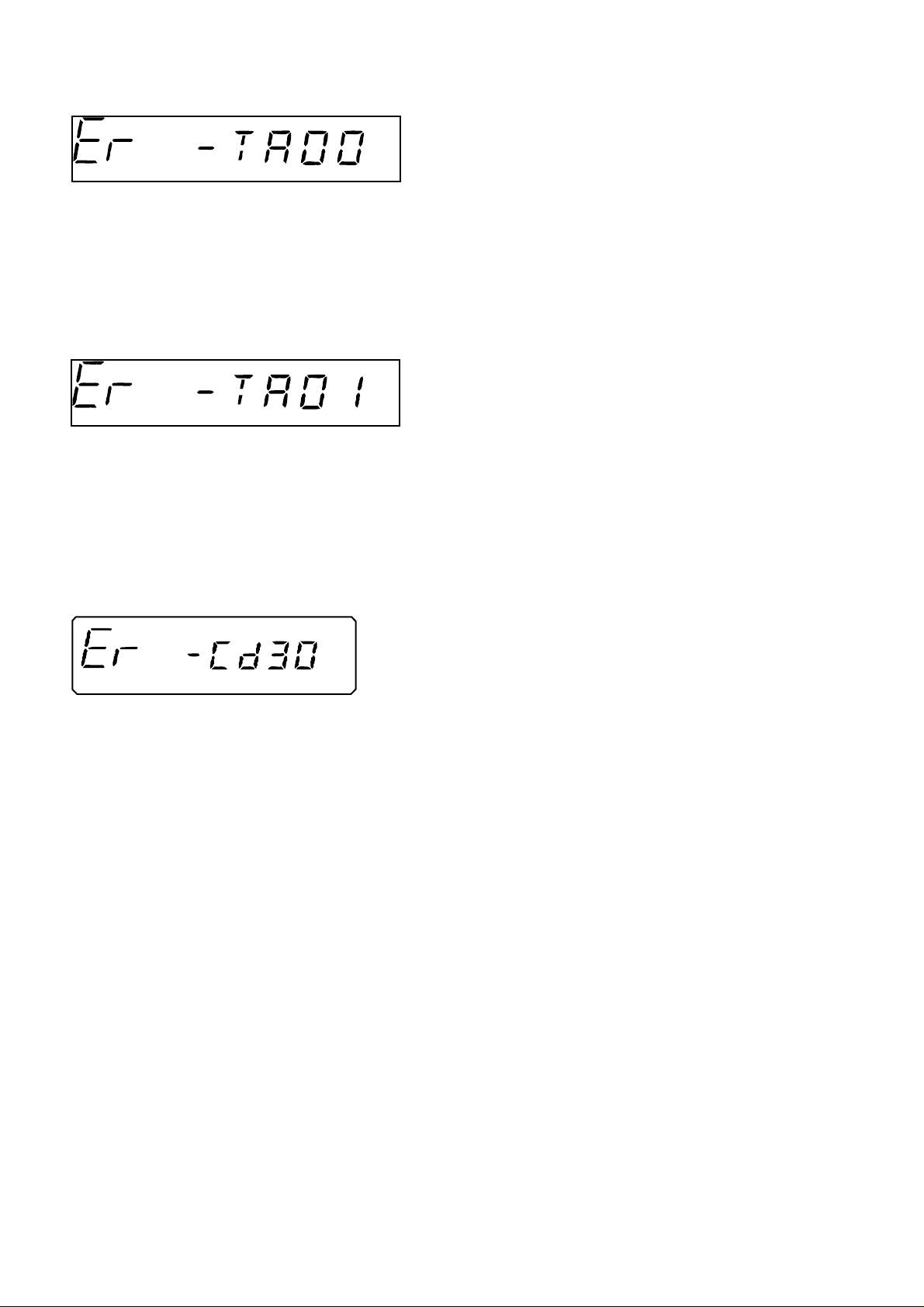
ERROR LIST
PU-IN SW detection error display
Error contents ............................ Displayed when the ON of detection SW could not be detected even after a certain period of time
passed, even though controlled to return the CD pickup to the most inside periphery in
microcomputer.
Major causes ............................. Failure of PU-IN SW or connection failure, and failure of slide motor or connection failure
Recovery method from error ..... Remove the cause of the error and turn on the power again.
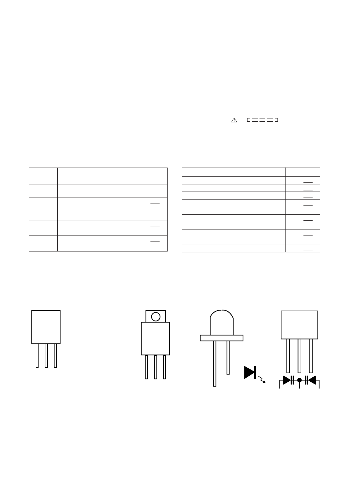
CD Read error display
Error contents ............................ Displayed when the data of the DISC can not be read correctly, or can be read however the
standard of the disc is impossible to be played back.
Major cause ............................... The disc is back to front. Other disc than CD-DA/VCD1.1/VCD2.0 is inserted.
The flaw or contamination of the disc is great and the data cannot be read.
Recovery method from error ..... Open the CD cover and insert a correct disc correctly. Remove the contamination or flaw of the
disc.
NO DICS display
Error contents ............................ Displayed when impossible to focus on the disc.
Major cause ............................... The disc is back to front. Other disc than CD-DA/VCD1.1/VCD2.0 is inserted. The flaw or
contamination of the disc is great and the data cannot be read.
Recovery method from error ..... Open the CD cover and insert a correct disc correctly. Remove the contamination or flaw of the
disc.
– 17 –
Page 18
XL-30V
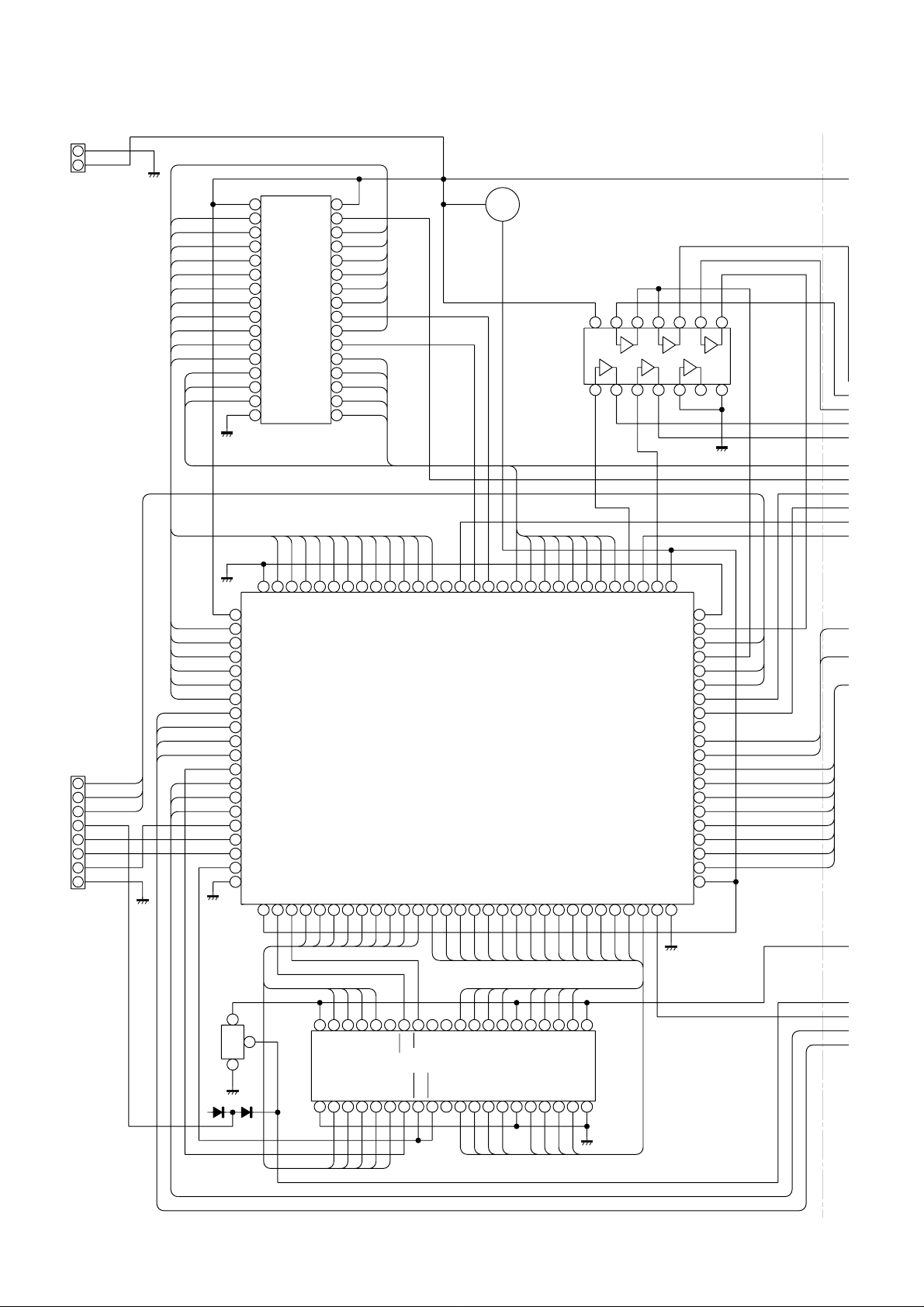
TAPE mechanism error display (1)
Error contents ............................ Displayed when not becomes "ON" while the mechanism operating detection SW "CAM-SW" is
being operated even though the motor or solenoid are controlled to operate the tape for playback/
FF/REW/Recording.
Major cause ............................... When displayed even though the mechanism is working, failure of CAM-SW and connection
failure.
When the mechanism is not working, failure of the motor and solenoid and connection failure.
Recovery method from error ..... Remove the cause of the error and turn on the power again.
TAPE mechanism error display (2)
Error contents ............................ Displayed when the initialization cannot be completed, even though the microcomputer controls
the motor or the solenoid to initialize the tape mechanism (set the mechanism to the stop
condition.) (Mechanism operating detection SW "CAM-SW" is stopped and does not become
"OFF".)
Major cause ............................... When displayed even though the mechanism is working, failure of CAM-SW and connection
failure.
When the mechanism is not working, failure of the motor and solenoid and connection failure.
Recovery method from error ..... Remove the cause of the error and turn on the power again.
VCD unit communication error
Error contents ............................ The system computer cannot communicate with VCD unit microcomputer. Or can communicate
however the contents are not as specified in the specification.
Major cause ............................... VCD microcomputer or the CD servo microcomputer are in abnormal operation.
The power is not supplied to the VCD unit and CD servo unit.
The communication line between the system microcomputer and the VCD unit are short-circuit
or open.
Recovery method from error ..... Remove the cause of the error and turn on the power again.
– 18 –
Page 19
NOTES ON SCHEMATIC DIAGRAM
XL-30V
• Resistor:
To differentiate the units of resistors, such symbol as K and
M are used: the symbol K means 1000 ohm and the symbol
M means 1000 kohm and the resistor without any symbol is
ohm-type resistor. Besides, the one with “Fusible” is a fuse
type.
• Capacitor:
To indicate the unit of capacitor, a symbol P is used: this
symbol P means pico-farad and the unit of the capacitor
without such a symbol is microfarad. As to electrolytic
capacitor, the expression “capacitance/withstand voltage”
is used.
(CH), (TH), (RH), (UJ): Temperature compensation
(ML): Mylar type
(P.P.): Polypropylene type
• Schematic diagram and Wiring Side of P.W.Board for this
model are subject to change for improvement without prior
notice.
REF. NO DESCRIPTION POSITION
NSW801 PICKUP IN ON—OFF
SW651 VOLTAGE SELECTOR 110V-127V
—220-240V
SW700 JOG ON—OFF
SW709 ON/STAND-BY ON—OFF
SW710 CLOCK/TIMER/SLEEP ON—OFF
SW711 TUNING UP ON—OFF
SW712 PLAY/CD PAUSE ON—OFF
SW713 VOLUME SELECT ON—OFF
SW721 MEMORY/SET ON—OFF
• The indicated voltage in each section is the one measured
by Digital Multimeter between such a section and the chassis with no signal given.
1. In the tuner section,
( ) indicates AM
< > indicates FM stereo
2. In the main section, a tape is being played back.
3. In the deck section, a tape is being played back.
( ) indicates the record state.
4. In the power section, a tape is being played back.
5. In the CD section, the CD is stopped.
• Parts marked with “ ” ( ) are important for
maintaining the safety of the set. Be sure to replace these
parts with specified ones for maintaining the safety and
performance of the set.
POSITIONREF. NO DESCRIPTION
SW722 BASS/TREBLE ON—OFF
SW723 BAND ON—OFF
SW724 REC. PAUSE ON—OFF
SW725 STOP/CLEAR ON—OFF
SW726 TUNING DOWN ON—OFF
SW727 FUNCTION ON—OFF
SW728 VOLUME/JOG ON—OFF
SW801 OPEN/CLOSE ON—OFF
SW901 FOOL PROOF ON—OFF
SW902 CAM ON—OFF
FRONT
VIEW
ECB
(1) (2) (3)
TYPES OF TRANSISTOR AND LED
2SA933 SR
2SB562 C
2SC2001 K
2SC535 C
2SD1858 R2
KRA102 M
KRC102 M
KRC104 M
KRC107 M
KTA1266 GR
KTC3199 GR
FRONT
VIEW
BCE
2SD2012 Y
– 19 –
FRONT
VIEW
MPG3372X
HY2043
1 2 3
SVC348S
KDV147B
Page 20
XL-30V
V_GND
2
V_5V
1
TO CD PWB
CNP810
VPP
VCC
1
2
3
4
5
6
7
8
9
10
11
12
13
14
15
16
A16
A15
A12
A7
A6
A5
A4
A3
A2
A1
A0
D0
D1
D2
VSS
A18
A17
A14
A13
A8
A9
A11
OE
A10
CE
D7
D6
D5
D4
D3
32
31
30
29
28
27
26
25
24
23
22
21
20
19
18
17
IC10V
IX0035SJ
ROM 256K x 16
REGULATOR
Q11V
3.3V
IC17V
74HC07A
1 2 3 4
BUFFER AMP.
VCC
10 11 12 13 14
5
9
6
8
GND
7
MPACK
8
MPDATA
7
MPSTB
6
MPRST
5
DATA
4
LRCK
3
TO CD PWB
BCK
2
D_GND
1
CNP808
81
VCC
LA12
82
LA13
83
LA14
84
LA15
85
LA16
86
LA17
87
AUDIO_CLK
88
AUDIO_DATA
89
BCLK
90
LR
91
DRAS1/DOE
92
RSD
93
RBCLK
94
RWS
95
TDMCLK
96
TDMDR
97
TDMFS
98
DCAS
99
VSS
100
1 2 3 4
IC13V
RESET
KIA7036P
1
3
2
VSS
VCC3
LA4
LA5
LA6
LA7
LA8
LA9
LA10
LA11
DRAS
DWE
DA0
DA1
DA2
DA3
DA4
DA5
8
9
6
5
7
20 19 18 17 16 15 14 13 12 11 10
A0
A1
A2
A3
VCC
51 52 53 54 55 56 57 58 59 60 61 62 63 64 65 66 67 68 697071727374757677787980
LA0
LA1
LA2
LA3
LSCE0
LSCE1
LOE
LROMCE
LWR
LD7
LD6
LD5
LD4
LD3
LD2
LD1
LDO
AUX1/DSADATA
IC15V
ES3880F
VIDEO CD DECODER
DA6
DA7
DA8
DBUS0
DBUS1
DBUS2
DBUS3
DBUS4
DBUS5
DBUS6
DBUS7
DBUS8
DBUS9
DBUS10
DBUS11
DBUS12
10 11 12 13 14 15 16 17 18 19 20 21 22 23 24 25 26 27 28 29 30
D1
D2
D3
D4
D5
D6
D7
WE
RAS
VCC
DBUS13
1 2 3 4 5 6 7 8 9
D0
VCC
VCC3
VSSK
/MRQ
AUX6
AUX5
AUX4
/BUSY
DSC_STB
AUX7/SCK
AUX3/DSASTB
AUX2/DATA
AUX0/DSAACK
PCLKQSCN
PCLK2XSCN
DCLK
HSYNC
VSYNC
YUV7
YUV6
YUV5
YUV4
YUV3
YUV2
YUV1
YUV0
VCC3
DBUS14
DBUS15
RESET
VSS
5 0
49
48
47
46
45
44
43
42
41
40
39
38
37
36
35
34
33
32
31
VSS A4A5A6A7A8OE
21
22 23 24 25 26 27 28 29 30 31 32 33 34 35 36 37 38 39 40
LCASD8D9
UCAS
D10
D11
VSS
D12
D13
D14
D15
IC16V
IX0025SJ
D-RAM 256K x 16
Figure 20 BLOCK DIAGRAM (1/6)
– 20 –
VSS
Page 21
IC11V
NJM4555M
BUFFER AMP.
XL-30V
7
- + + -
6
5
8
XL100V
27MHz
27MHz
80 79 78 77 76 75 74 73 72 71 70 69 68 67 66 65 64 63 62 61 60 59 58 57 56 55 54 53 52 51
XIN
VSS
VSS
81
82
83
84
85
86
87
88
89
90
91
92
93
94
95
96
97
98
99
100
HSYNC
DSC_D6
VSYNC
DSC_D5
YUV7
YUV6
YUV5
YUV4
VCC
VSS
YUV3
DSC_D4
YUV2
DSC_D3
YUV1
DSC_D2
YUV0
DSC_D1
VSS
PCLK
DSC_D7
PCLK2X
VSS
1 2 3 4
VCC
VSS
5
VCC
DSC_CLK
6
AUX0
7
VCC
XOUT
AUX3
AUX4
AUX5
VIDEO CD ENCODER
DSC_D0
AUX1
DSC_STB
AUX2
DCLK
8
9
RST
1110 12 13 14 15 16 17 18 19 20 21 22 23 24 25 26 27 28 29 30
1
2
3
4
VCC
AUX6
ACAP
VDAC
IC14V
ES3883F
AUX7
MUTE
VCC
MCLK
VSSAV
VSSAV
AUX8
TWS
YDAC
AUX9
VCCA
TSD
VCCA
TBCK
CDAC
RWS
V_AMP
VSSAV
VSSAV
RSTOUT
VSS
RSET
COMP
VSS
SQCK
Q12V
VSSA
VREF
MIC2
VREFM
MIC1
AOL+
AOL-
AORAOR+
VCCA
VREFP
VCM
VSSA
AUX15
AUX14
LA18/AUX13
RBCK
AUX12
AUX11
AUX10
RSD
VCC
VSS
SQSO
50
49
48
47
46
45
44
43
42
41
40
39
38
37
36
35
34
33
32
31
R_CH
A_GND
L_CH
A_12V
VDAC
V_GND
VD_DO
VD_DI
BUSY
SCK
VD_STB
BI606
1
2
3
4
2
1
1
2
3
4
5
CNP809
TO MAIN PWBTO CD PWB
CNP607
CNS606
1
2
3
4
TO MAIN PWB
AUDIO_CLK LRAUDIO_DATA
Figure 21 BLOCK DIAGRAM (2/6)
– 21 –
BCLK
Page 22
XL-30V
S
N
P
V
P
3
1
BUS1
~
1 4
LCD701
5
24
~
SWITCHING
Q707
Q706
D704-709
LED
CFW701
SWITCHING
M_12V
SWITCHING
LED+B
Q708
RESET
Q701
A_12V
Q709
Q702
Q703
RX701
REMOTE
SENSOR
2
3
SW700
1
JOG
100
99
98
97
1
2
3
4
5
6
7
8
9
X701
8MHz
X702
32.768kHz
SW709-SW710
KEY
SW711-SW713
SW721-SW728
C
A
B
UP
DOWN
U-COM VDD
U-CON+5V
SYS STOP
REMOCON
RESET
P CONT
3
TO
POWER
2
PWB
1
CNS707
10
11
12
13
14
15
16
17
18
19
20
21
22
23
24
25
DI
SEG1
SEG0
COM1
COM0
VLC3
VLC2
VLC1
VDD
OSC2
OSC1
VSS
XI
XO
MMOD
VREF
CLID_SW
KEY1
KEY2
MODEL
CLID_PRO
TAPE_SW
VREF+
DO
CL
26
27
SEG2
VCD_OUT
28
29
SEG3
1
2
VCD_IN
96
SEG4
COM3
COM2
VCD_CLK
30
95
SEG5
VCD_BUSY
31
92
93
91
94
SEG9
SEG8
SEG7
SEG6
SYSTEM CO
MICROCOM
RESET
CD_STB
CE
33
34
32
35
89
90
SEG11
SEG10
IX0030
CLOCK
POWER
36
37
88
87
SEG13
SEG12
IC701
SYS STOP
REMOCON
39
38
86
SEG14
VCD_STB
40
SW801
OPEN/CLOSE
TO VIDEO PWBTO VIDEO PWB
TO DISPLAY PWB
1
2
3
4
5
CNS809
CNS808
1
2
3
4
5
6
7
8
CNP702
CD_STB
1
VD_STB
2
SCK
3
BUSY
4
VD_DI
5
VD_DO
6
CLID_OUT
7
CLID_SW
8
VD_DO
1
VD_DI
2
BUSY
3
SCK
4
VD_STB
5
BI809
BI808
D_GND
1
BCK
2
LRCK
3
AOUT
4
MP RST
5
MP STB
6
MP DATA
7
MP ACK
8
CFW807
X801
16.9344MHz
48 47 46 45 44 43 42 41 40 39 38 37 36 35 34 33
XI
49
50
51
52
53
54
55
56
57
58
59
60
61
62
63
64
RO
DVDD
DVR
LO
DVSS
ZDET
VSS
BUSO
BUS1
BUS2
BUS3
BUCK
/CCE
RST
VDD
1 2 3 4
XVDD
BCK
XO
LRCK
XVSS
TESIN
TC9490F
SERVO SIGNAL
CONTROL
AOUT
IPF
DOUT
6
5
DVSS
DVDD
IC802
17
DVSS
DVDD
8
7
SEL
FMO
DMO
AVDD3
TMAX
SBOK
CLCK
DATA
SFSY
10 11 12 13 14 15
9
TEBC
SBSY
VREF
RFGC
PVREF
/HSO
X802
8MHz
TRO
TEI
SBAD
FEI
RFRP
RFZI
RFCT
AVDD
RFI
SLCO
AVSS
VCOF
LPFO
LPFN
/UHSO
PVDD
16
FOO
PDO
10 11
MECHA
12
TEST
13
/RESET
14
XIN
15
XOUT
16
AVSS
17
VAREF
18
TSW1A
19
TSW1B
20
TSW2A
21
22
MICROCOM
TSWUP
23 24 25 26 27 28 29 30 3
+5V +5V
TEZI
32
31
30
29
28
27
26
25
24
23
22
21
20
19
18
17
TRY+
PUNSW
IX0031S
CD SER
6
789
TRY-
CCE
IC806
5
BUCK
4
BUS0
Figure 22 BLOCK DIAGRAM (3/6)
– 22 –
Page 23

SEG4
VCD
CLK
701
5
~
92
93
91
94
SEG6
SEG7
SEG8
90
SEG9
6
COM3
95
SEG5
SYSTEM CONTROL
MICROCOMPUTER
_
VCD_BUSY
RESET
CD_STB
CE
33
31
34
0
36
32
35
24
89
88
87
86
SEG13
SEG12
SEG11
SEG10
IC701
IX0030SJ
CLOCK
SYS STOP
REMOCON
POWER
39
38
37
40
85
SEG15
SEG14
VCD_STB
JOG_UP
42
41
84
SEG16
49
50
VCD_IND
82
83
SEG18
SEG17
75
74
SURR
JOG_DOWN
SOL
MOT
43
44
81
SEG25
SEG26 COM2
REC
45
80
SEG19
46
79
78
SEG21
SEG20
CLID_OUT
MVOL_DW
MVOL_UP
MVOL_IND
RUN_PLS
BIAS
48
47
77
SEG22
SEG27
SEG28
SEG29
SEG30
SEG31
SEG32
SEG33
CLID_DW
CLID_UP
STEREO
B-LIGHT
P-CONT
CD+B
P-MUTE
P-STB
B-CAN
49
76
SEG23
SD
50
75
74
SEG24
73
72
71
70
69
68
67
66
65
64
63
62
61
60
59
58
57
56
55
54
53
52
51
IC702
MVOL_DW
TA7291S
LOADING MOTOR DRIVER
1 2 3 4
M_12V
XL-30V
CL ID_SW
VD_DO
VD_DI
BUSY
SCK
VD_STB
CD_STB
A_12V
M_12V
D_GND
SOL
MOT
REC
RUN_PLS
BIAS
B_CAN
SD
DO
CL
CE
DI
CD+B
CFW704
8
7
6
5
4
3
2
1
CNS702
11
10
9
8
7
6
5
4
3
2
1
CNP703
9
1
TO CD PWB
TO MAIN PWB
TO MAIN PWB
CLID_OUT
MVOL_UP
TAPE_SW
U_CON5V
8
7
9
M701
JOG MOTOR
6
5
M
STEREO
P_MUTE
P_STB
10 11
6
789
MECHA
12
TEST
13
/RESET
14
XIN
15
XOUT
16
AVSS
17
VAREF
18
TSW1A
19
TSW1B
20
TSW2A
21
22
+5V +5V
TRY-
CCE
TRY+
PUNSW
IC806
IX0031SJ
CD SERVO
MICROCOMPUTER
TSWUP
23 24 25 26 27 28 29 30 31 32 33
4321
5
BUS0
BUCK
BUS1
MPRST
BUS2
DATA
44
ACK
BUS3
43
42
STB
41
VDD
40
39
38
37
36
35
34
13
14
FEI
15
16
RFRP SEL
17
18
RFI
19
RFGC
20
21
22
23
24
SERVO AMP.
GVSW
VRO
FEO
FEN
RFRP
RFIS
RFGO
RFGC
AGCI
RFO
RFN
GND
IC801
TA2147F
IC807
KIA7805AP
VOLTAGE
REGULATOR
+5V
+5V
Q861
IC804
LA6548D
FOCUS/TRACKING/
SBAD
RFDC
12
TEI
TEO
11
10
TEN
TEBC
TEB
9
SEL
8
LDOx
7
MDI
6
E
5
TN1
F
4
TPI
B
3
FPI
A
2
FNI
1
VCC
CD_8V
1 3
2
SL+
SL-
FMO
REG
101112131415
IN
REG
OUT
REG.
RESET
RES
CD
16 17 18 19 20 21 22 23 24 25 26 27 28 29 30
SPIN/SLED DRIVER
TRO
TR-
TR+
SP-
8
9
6
5
7
FO-
FO+
SWITCHING
Q801
SP+
DMO
CD STB
2 3 4
FOO
+5V
1
VCC
MUTE
VCC
PU-IN
SP+
SP-
SL+
SL-
VREF
+5V
TRTR+
FO+
FO-
D-GND
CD_GND
PD
VR
LD
M_GND
CD_8V
V_GND
C
F
B
A
E
1/2V
+5V
M_12V
V_5V
1 2 1
1
2
3
4
BI605B
1 2 1
BI605A
CNS605A
2
CNS605B
1
2
3
4
2
BI810
CNS810
+
NM802
M
-
SPINDLE MOTOR
+
NM801
M
-
SLED MOTOR
NSW801
PICKUP IN
PICKUP UNIT
TO MAIN PWB
TO POWER PWB
TO VIDEO PWB
TR-
TR+
FO+
FO-
ACTUATOR
1/2VCC
C
F
B
A
E
GND
MON
LD
LT0H41M1
VCC
Figure 23 BLOCK DIAGRAM (4/6)
– 23 –
Page 24

XL-30V
E
L
AM
ANTENNA
TERMINALS
SO301
FM ANTENNA
TERMINALS
BF301
BAND
PASS
FILTER
CNP301
1
2
FM RF
L302
VD303
FM FRONT END
VT
IC301
TA7358AP
T306
AM OSC.
78654323211
T302
AM ANT.
FM IF FM IF
T304
CF303
FM OSC
VT
L303
VD302
9
VD301-1
SVC348S
VD301-2
SVC348S
Q305
FM+B
FM IF
AMP.
Q306
VT
FM MUTE LEVEL
VR351
10K(B)
AM OSC OUT
FM IF
CF302
X352
4.5MHz
24
23
AM OSC OUT
FM IF IN
AM MIX OUT
21
22
FM AFC
AM RF IN
AM OSC IN
REG
AM MIX OUT
AM IF
T351
TP301
21
22
20
VSS
AOUT
X OUT
X IN
1 2 3 4
20
VSM
AM IF IN
GND
4 3 2 1
5
AM IF IN
CF352
IC302
LC72131
PLL(TUNER)
19
18
AIN
CE
DI
X351
18
7
17
VDD
DO
FM/AM OUT
LA1832
FM DET
STEREO
8
15
16
FM IN
FM
MUTE
8
7
456kHz
IC303
14
AM IN
FM
9
19
AM LOW CUT
FM IF DET./FM MPX./AM IF
SD
6
+5V
PD
CL
6
5
+5V
13
10
9
12
SW
IF IN
MO/ST
11
17
MPX VCO
VCC
IF REQ
16
10
MPX IN
IF OUT
11
PHASE
15
R-CH OUT
13
14
L-CH OUT
PHASE
12
MO/ST
(AM/FM)
SWITCHING
+5V
Q351
FM+B
ZD351
R_MUTE
R-MUTE
FM RIPPLE
FILTER
Q360
A_12V
A_12V
STER
RECORD/
PLAYBACK
HEAD
L-CH
R-CH
ERASE
HEAD
M901
TAPE MOTOR
M
SOL901
SOLENOID
SD
REC
REC
A_12V
A_12V
TAPE SW
10
11
TAPE
IC101
HEAD SELECTOR
BA3126N
REC SW
L-CH
1
2
L-CH
3
P/B SW
CONT
4
5
6
7
8
9
BIAS OSC
Q151
L151
Q172
SWITCHING
IC101
P/B SW
REC SW
REC
SWITCHING
Q152
Q153
A-12V
R-CH
R-CH
SWITCHING
Q171
A_12V
PH901
PHOTE INTERRUPTER
CFM901
+
-
SW901
FOOL
PROOF
SW902
CAM
A_12V
SWITCHING
REC BIAS
CONT
SOLENOID
DRIVER
Q101-Q104
SWITCHING
IC102
BA3311L
REC./P.B.
EQUALIZER AMP.
SWITCHING
Q903
Q902
Q901
SWITCHING
L-IN
5
9
R-IN
RUN PLS
SOL
M_12V
Q905
TAPE MOTOR
DRIVER
NF
3
150K
+
MUTE
+
150K
11
NF
SWITCHING
6
Q906
SWITCHING
Q904
ALC
7
U_CON5V
1
12
MOT
CNP703
L-OUT
R-OUT
10
8
2
ALC
B-CAN(NC)
1 2 3 4
A_12V
BIAS
RUN_PLS
REC
MOT
5
TO DISPLAY PWB
Q105
Q106
REC MUTE
D-GND
SOL
U_CON 5V
8
6
7
M_12V
M_12V
9
Figure 24 BLOCK DIAGRAM (5/6)
– 24 –
Page 25

XL-30V
L
NG
R_MUTE
51
R-MUTE
FM RIPPLE
FILTER
Q360
Q105
Q106
REC MUTE
A_12V
A_12V
M_12V
REC
STEREO
SD
REC L/R CH
TAPE L/R CH
FM ST
CD+B
P MUTE
P-STB
CNS704
SD
DO
CL
CE
DI
9
8
7
6
TO DISPLAY
5
PWB
4
3
2
1
FROM CD PWB
MECHA 12V
(M_12V)
AUDIO 12V
(A_12V)
MUTE
REGULATOR
Q605
VOLTAGE
REGULATOR
Q604
CNP654
V_5V
1
2
CD_8V
3
4
Q601
Q602
VOLTAGE
VOLTAGE
REGULATOR
IC682
KIA7805AP
VOLTAGE
REGULATOR
Q603
Q672
TAPE R
TUN R
CD R
CD L
TUN L
TAPE L
L-IN
R-IN
T1A L 250V
CD+B
1 3
2
REG.
Q671
SWITCHING
FROM
DISPLAY PWB
P-CONT
F653
15
16
10
8
9
Q673
Q608
CNP707
14
13 12
IC401
LC75342M
18
17
IC601
LA4600
POWER
AMP.
VCC
7
4
F656
T500mA L 250V
Q609
SWITCHING
3
2
1
REC R-CH
11
10
FUNCTION/VOLUME EQUALIZER
19
20
21
REC L-CH
L-CH OUT
1
R-CH OUT
3
2
D651~D654
VOLTAGE
REGULATOR
D661~D664
IC681
KIA7805AP
VOLTAGE
REGULATOR
3
2
R-CH OUT
8
9
7
24
23
22
Q681
1
6
25
L-CH OUT
T1.6A L 250V
5
26
L-CH
F651
T2.5A L 250V
F654
VSS
NC
28
+
+
HEADPHONES
L-CH
MAIN POWER
TRANSFORMER
RLY681
CE
LOGIC
VDD
29
A_12V
SO601
SPEAKER
TERMINALS
J601
T651
4 3 2 1
27
DI
30
CL
T.F
Q683
T681
SUB POWER
TRANSFORMER
220-240V
110-127V
SW651
VOLTAGE
SELECTOR
SO651
AC POWER INPUT
AC110-127/220-240V,
50/60Hz
SOL
U_CON 5V
6
7
AY PWB
M_12V
D-GND
8
9
A_12V
A_12V
TAPE SW
10
11
A_12V
4
CD L
3 2 1
CD R
M_12V
D681~D684
CNP605
2
1
TO CD PWB TO VIDEO PWB
Figure 25 BLOCK DIAGRAM (6/6)
– 25 –
Page 26

XL-30V
R
3
8
R
A
P29 12 - C
TO VIDEO PWB
P33 12 - C
CNS702
FROM
DISPLAY PWB
B
CNP809
CNS809
1
2
3
4
5
BI809
VD_DO
1
VD_DI
2
BUSY
3
SCK
4
VD_STB
5
CD_STB
1
VD_STB
2
SCK
3
BUSY
4
VD_DI
5
VD_DO
6
CLID_OUT
7
CLID_SW
8
X802
8MHz
R837
10K
C844
0.1
CNP702
C
+B
XVDD
BCK
1
XO
2
R815
LRCK
3
22
C820
XI
AOUT
0.1
R890 33
R891 33
R892 33
+B
C827
47P(CH)
XVSS
DVSS
DVDD
TESIN
14
15
IC802
TC9490F
SERVO/SIGNAL
CONTROL
DVSS
DVDD
IPF
DOUT
5
8
4
6
7
13
+B
J851
33
+B
+B
D
+B
E
R819
220
+B
C830
0.056
C840
100/10
F
C835
0.056
+B
C836
100/10
C837
470P
C828
100/10
BUS0
BUS1
BUS2
BUS3
BUCK
/CCE
C825
C826
47P(CH)
X801
16.9344MHz
49
DVSS
50
RO
51
DVDD
52
DVR
53
LO
54
DVSS
55
ZDET
56
VSS
57
BUS0
58
BUS1
59
BUS2
60
BUS3
61
BUCK
62
/CCE
63
/RST
64
VDD
R813
22
0.1
R818
1M
R820
1K
48 47 46 44 43 42 41 40 39 38 37 36 34 333545
G
H
• NOTES ON SCHEMATIC DIAGRAM can be found on page 19.
• The numbers 1 to 15 are waveform numbers shown in page 41.
1
23456
Figure 26 SCHEMATIC DIAGRAM (1/9)
– 26 –
DMO
SBOK
9
+B
FMO
CLCK
10
AVDD3
4
DATA
11
SEL
SFSY
12
TEBC
SBSY
13
GND
RFGC
11
/HSO
14
VREF
6
8
/UHSO
15
+B
TRO
5
PVDD
1
1
C818
0.047
FOO
TEZI
TEI
SBAD
FEI
RFRP
RFZI
RFCT
AVDD
RFI
SLCO
AVSS
VCOF
PVREF
LPFO
LPFN
TMAX
PDO
16
R801
5.6K
AOUT
LRCK
BCK
2
3
4
2
3
4
CNP808
P28 1 - E
TO VIDEO PWB
C819
0.047
C817
0.047
R809
4.7K
32
31
30
29
28
27
26
25
24
23
22
21
20
19
18
17
MPRST
5
5
1
12
R802
47K
MPSTB
6
6
1
2
C808
0.033
R804
120K
MPACK
MPDATA
8
7
8
7
OPEN/CLOSE
SWITCH PWB-A6
CFW807
1
2
C823
0.01
220/10
C821
0.047
C810
0.001
C809
0.001
47/10
7
C807
0.033
R807
10K
C806 0.01
C805 0.0027
C804 0.01
C802
0.015
R806
15K
C801
47P
BI808
CNS808
C822
C811
C803
47/10
SW801
OPEN/CLOSE
+B
+B
0.01
C812
+B
L803
10µH
C813
100/10
C863
470P
C838
0.0068
R839
2.2K
L801
10µH
C842
0.1
R831
3.3K
+B
C845
100/10
C831
0.1
R82
1K
C848
56P
R829
39K
C849
0.056
C850
220/10
+B
Page 27

X802
8MHz
R839
2.2K
L801
10µH
R837
10K
C844
0.1
R848
33
R836
2.2K
11 10 9 8 7 6 5 4 3 2 1
12
13
14
15
16
17
18
19
20
21
22
R838
33K
MECHA
TEST
/RESET
XIN
XOUT
AVSS
VAREF
TSW1A
TSW1B
TSW2A
TSW2B
TRY+
PUNSW
MICROCOMPUTER
TSWUP
23
2625
24
R846 33
R847 33
CCE
TRY-
BUS0
BUCK
IC806
IX0031SJ
CD SERVO
28
29
27
R835 10K
30
IC804
C857
47/16
+B
R834 10K
R845 33
BUS1
31
32
LA6548D
FOCUS/TRACKING/
SPIN/SLED DRIVER
10K
R843 33
R844 33
BUS2
BUS3
ACK
44
DATA
43
42
STB
41
MPRST
40
VDD
39
38
37
C832 0.01
36
35
34
33
R861
Q861
2SB562 C
2.2K
6.4V3.3V
+B
10 9
11
12
13
15
14
VIN2
VG2
VO2-
VO2+
REG_IN
REG_OUT
CD
RESET
VG3
VIN3
VO3+
16 17 18 19 20 21 22 23 24 25 26 27 28 29 30
VO3-
+B
R832
R833 10K
R842
R893
10K
R894
R841
10K
R840
R895
10K
R896
+B
3
C853
0.1
C833
47/10
C834
220/10
IC807
KIA7805AP
VOLTAGE
REGULATOR
+B
6
GND
3
7
4
5
VG1
GND
VO1-
VO1+
8
GND
3 2
VG4
GND
GND
GND
VO4+
VO4-
R863
33
33
33
33
R862
VIN1
VIN4
2.2K
2
2.2K
2
MUTE
VREF
1
+B
C854
VCC
VCC
0.1
MPACK
MPDATA
MPSTB
MPRST
1
+B
D801
1N4004
D802
1N4004
C860 0.1
C859 470/10
XL-30V
+B
C891
0.001
C890
0.0027
+B
+B+B
M_GND
M_12V
CD_GND
CD_8V
V_GND
V_5V
V_5V
V_GND
SP+
SP-
SL+
SL-
PU-IN
GND
BI605A
1
2
1
2
3
4
BI605B
1
2
BI810
BI803
6
5
4
3
2
1
CNS605ACNS605B
P31 8 - H
1
CNP605
2
TO MAIN PWB
1
P34 1 - D
2
CNP654
3
TO POWER PWB
4
P28 1 - B
1
CNP810
2
TO VIDEO PWB
CNS810
CD MOTOR PWB-C
CNS803
CNP803
SP+
6
6
SP-
5
5
SL+
4
4
SL-
3
3
PU-IN
2
2
GND
1
1
+
NM802
SPINDLE
M
-
MOTOR
+
NM801
M
SLED
-
MOTOR
NSW801
PICKUP IN
838
.0068
R849
C842
0.1
R831
3.3K
+B
C845
100/10
C831
0.1
R828
R826
10K
1K
C848
56P
R827
R829
3.3K
39K
C849
0.056
C850
220/10
+B
C846
0.1
C839
1P(CH)
C847
R823
0.1
100
R825
13
14
15
82K
16
17
18
19
20
21
22
23
24
C855
100/10
820
GVSW RFDC
VRO
FEO
FEN
RFRP
RFIS
RFGO
RFGC
AGCI
RFO
RFN
GND
TEO
TEN
10
TEB
SEL
LDO
MDI
TNI
TPI
9
FPI
FNI
VCC
IC801
TA2147F
SERVO AMP.
C841
100/10
+B
R822
10
3.3V
Q801
2SB562C
1.6V
C843
0.1
+B
+B
R80E 82K
R80A 82K
R80F 82K
R80G 56K
R821
150
R80B 56K
R80C 82K
C889
0.1
+B
12
11
R824
10
82K
9
8
7
6
5
4
3
2
1
TR+
FO+
GND
VREF
+5V
TR-
FO-
1
2
3
4
5
PD
6
VR
7
LD
8
BI801
C
1
F
2
B
3
A
4
E
5
6
7
BI802
CD PWB-A3
1
2
3
4
5
6
7
8
CNS801
1
2
3
4
5
6
7
CNS802
TR-
1
TR+
2
FO+
3
FO-
4
GND
5
PD
6
VR
7
LD
8
C
1
F
2
B
3
A
4
E
5
1/2V
6
+5V
7
PICKUP UNIT
TRTR+
FO+
FO-
ACTUATOR
1/2VCC
C
F
B
A
E
MON
GND
LD
VCC
+
+
+
+
+
-
7
8 9 10 11 12
Figure 27 SCHEMATIC DIAGRAM (2/9)
– 27 –
Page 28

XL-30V
A
P27 12 - C
FROM CD PWB
B
C
CNS810
2
1
CNP810
V_GND
V_8V
+B +B
+B
IC10V
IX0035SJ
ROM 256Kx16
+B
VPP
1
PGM/A18
A16
2
A15
3
A12
4
A7
5
A6
6
A5
7
A4
8
A3
9
A2
10
A1
11
A0
12
D0
13
D1
14
D2
15
VSS
16
C125V
100/10
VCC
A17
A14
A13
A11
OE
A10
CE
C105V
C115V
32
100/10
31
30
29
28
A8
27
A9
26
25
24
23
22
D7
21
D6
20
D5
19
D4
18
D3
17
Q11V
2SD1858R2
0.1
R143V
100
ZD101V
MTZJ4.3A
C112V
0.1
+B
4.3V
C126V
+B
3.6V5V
C128V
100/10
0.1
+B
R98V
4.7K
R90V
10K
+B
14 13 12 11 10 9 8
R91V
4.7K
+B
IC17V
74HC07A
VCC
GND
7654321
+B
R97V
4.7K
AMP.
BUFFER
R93V
+B
4.7K
R96V
4.7K
+B+B
D
E
F
G
MPDATA
CNS808
P26 4 - H
FROM CD PWB
MPACK
MPSTB
MPRST
DATA
LRCK
BCK
D_GND
R153V 33
8
7
6
5
4
3
2
1
CNP808
R154V 33
R155V 33
R161V 33
R166V 33
R168V 33
R169V
R158V
33
R159V
33
C107V
0.1
C108V
33
R157V
33
R156V
+B
1
0.01
2
IC13V
KIA7036P
RESET
D107V
DA204K
R95V
6.8K
4.7K
R162V
4.7K
3
R160V
4.7K
C110V
80 79 78 77 76 75 74 73 72 71 70 69 68 67 66 65 64 63 62 61 60 59 58 57 56 55 54 53 52 51
C109V
100/10
VSS
LA10
LA11
VCC
81
LA12
82
LA13
83
LA14
84
LA15
85
LA16
86
LA17
87
AUDIOCLK
88
AUDATA
89
BCLK
90
LR
91
DRAS1/DOE YUV7
92
RSD
93
RBCLK
94
RWS
95
TDMCLK
96
TDMDR
97
TDMFS
98
DCAS
99
VSS
100
VCC3
DWE
DRAS
0.1
+B
+B
2019181716151413121110987654321
0.1
A3A2A1
C111V
VCC
VSS
A4
LA5
LA6
LA7
LA8
LA9
DA4
DA3
DA2
DA1
DA0
A0
RAS
A8OEA7A6A5
D-RAM 256Kx16
LA0
LA1
LA2
LA3
LA4
VIDEO CD DECODER
DA8
DA7
DA6
DA5
987654321
D7D6D5D4D3D2D1
WE
UCAS
LCAS
IC16V
IX0025SJ
LSCE1
LSCE0
LROMCE
IC15V
ES3880F
DBUS3
DBUS2
DBUS1
DBUS0
VCC
VSS
D11
D10D9D8
LOE
DBUS4
0.1
C116V
D12
LWR
DBUS5
D13
D14
LD6
LD7
DBUS7
DBUS6
+B
D0
D15
4039383736353433323130292827262524232221
LD5
DBUS8
VCCVSS
LD3
LD4
DBUS10
DBUS9
C117V
0.1
LD1
LD2
DBUS12
DBUS11
C118V
LD0
SCK/AUX7
AUX3/DSASTB
AUX1/DSADATA
AUX0/DSAACK
DBUS14
DBUS13
100/10
+B
AUX5
VCC3
VSS
BUSY
DSC_STB
MRQ/AUX6
AUX4
AUX2/DATA
PCLKQSCN
PCLK2XSCN
DCLK
HSYNC
VSYNC
YUV6
YUV5
YUV4
YUV3
YUV2
YUV1
YUV0
VCC3
DBUS15
RESET
VSS
302928272625242322212019181716151413121110
C005
0.001
50
49
48
47
46
45
44
43
42
41
40
39
38
37
36
35
34
33
32
31
C004
0.001
0.1
C119V
0.1
C120V
(D_GND)
(GND_A)
+B
C121V
+B
+B
100/10
R163V
33
R164V
10
R165V
10
+B
+B
R167V
33
TP
27MHz
C127V
0.1
+B
+B
H
• NOTES ON SCHEMATIC DIAGRAM can be found on page 19.
• The numbers 16 and 17 are waveform numbers shown in page 41.
1
23456
Figure 28 SCHEMATIC DIAGRAM (3/9)
– 28 –
Page 29

XL-30V
96V
.7K
R163V
33
R164V
10
R165V
10
+B
+B
R167V
33
TP
27MHz
C127V
0.1
C150V
0.1
R102V
100K
R116V
15K
C167V
22P(CH)
C158V
R115V
15K
100/10
0.1
C169V
C168V
0.1
C160V
+B
22P(CH)
C161V
100/10
+B
C104V
100/10
R111V
R113V
150
Q12V
2SA933 SR
A_12V
Lch
GND_A
Rch
68
C101V
1000/6.3
R112V
10K
R137V
1K
R138V 1K
R139V 1K
R141V 1K
R140V 1K
4
3
2
1
BI606
VDAC
2
GND_V
1
BI607
VD_DO
1
VD_DI
2
BUSY
3
SCK
4
VD_STB
5
CNP809
4
3
2
1
CNS606
2
1
CNS607
CNP606
P31 8 - H
TO MAIN PWB
CNP607
P31 12 - E
CNS809
P26 1 - A
FROM CD PWB
TO MAIN PWB
IC11V
NJM4565M
BUFFER AMP.
R107V
18K
R189V
R187V
10K
C137V
10/25
10K
C143V
33P(CH)
C141V
C139V
10/25
33P(CH)
100K
R181V
16
18K
R185V
R183V
100K
7
6
5
C149V
R195V
100
- + + -
8
4
0.1
C147V
C148V
100/10
17
1
2
3
100/10
R104V
R103V
C144V
33P(CH)
R186V
18K
10K
6.8K
C140V
R182V
R184V
100K
10/25
R108V
18K
100K
C171V
10/25
C142V
33P(CH)
10K
R188V
C172V
10/25
R101V
100K
R190V
10K
C138V
10/25
+B
L103V
+B
3.3µH
+B
+B
470
L104V
3.3µH
0.1
C131V
0.001
R171V
L111V
C129V
10µH
27P
(CH)
C184V
+B
0.1
100K
10P
XL100V
TC100V
27MHz
+B
150
R178V
+B
0.1
C124V
C136V
R194V
80 79 78 77 76 75 74 73 72 71 70 69 68 67 66 65 64 63 62 61 60 59 58 57 56 55 54 53 52 51
XIN
VSS
VSS
22P(CH)
DSC_D7
HSYNC
DSC_D6
VSYNC
DSC_D5
YUV7
YUV6
YUV5
YUV4
VCC
VSS
YUV3
DSC_D4
YUV2
DSC_D3
YUV1
DSC_D2
YUV0
DSC_D1
VSS
PCLK
PCLK2X
VSS
C130V
VCC
0.1
C183V
81
82
83
84
85
86
87
88
89
90
91
92
93
94
95
96
97
98
99
100
+B
VSS
VCC
AUX3AUX2
XOUT
VIDEO CD ENCODER
AUX1
AUX0
DSC_STB
DSC_CLK
DSC_D0
VCC
987654321
C106V
1
R142V
5.6K
VCC
AUX6
AUX5
AUX4
IC14V
ES3883F
AUX7
MUTE
DCLK
RST
C135V
0.1
ACAP
VCC
VDAC
MCLK
VSSAV
AUX8
VCCA
VCCA
YDAC
VSSAV
AUX9
TWSTSTBCK
CDAC
RWS
VSSAV
VSSAV
RSTOUT
VSS
R193V
4.7K
RSET
COMP
NC/ AUX15
S_EN/ AUX14
LA18/ AUX13
NC/ AUX12
NC/ AUX11
NC/ AUX10
SQCK
VSS
VREFM
SQSO
VREF
MIC2
MIC1
AOL+
AOL-
AORAOR+
VCCA
VREFP
VCM
VSSA
RBCK
RSD
VCC
VSS
302928272625242322212019181716151413121110
VSSA
50
49
48
47
46
C162V
45
44
43
42
41
40
39
38
37
36
35
34
33
32
31
C164V
47/10
R100V
4.7K
C100V
10P
0.1
C165V
0.1
R94V
4.7K
+B
C166V
0.1
R105V
4.7K
100/10
C159V
VIDEO SIGNAL
BCLK
AUDATA
LR
AUDIOCLK
VIDEO PWB-F
7
8 9 10 11 12
Figure 29 SCHEMATIC DIAGRAM (4/9)
– 29 –
Page 30

XL-30V
M 12V
+
W
A
AM
GND
B
FM
SO301
FM ANTENNA
C
D
E
F
G
H
1
2
75 OHMS
CNP301
C301
0.001
D301
1N4148
D302
1N4148
C349
0.001
C376
0.001
D306
1N4148
1
2
BF301
BAND PASS
FILTER
RECORD/PLAYBACK
HEAD
L-CH
R-CH
ERASE HEAD
AM TRACKING
AM ANT.
T302
C331
0.047
C330
C329
0.022
+B
C337
0.022
C307
0.0047
C305
0.0047
C308
0.022
R301
22
FM RF
L302
C306 9P(UJ)
C304 0.01
D305 1N4148
C303
0.001
C319
18P
(CH)
123 4 56 7 8 9
3
CNP101
CNS101
1
1
2
2
3
3
4
4
5
5
6
6
7
7
8
8
MAIN PWB-A1
M901
TAPE
MOTOR
+
CFM901
1
M
-
2
SOL901
SOLENOID
12P(CH)
R323
C335
68K
560P
T306
AM OSC.
AM BAND
COVERAGE fL
R310
4.7K
R315
33
Q305
2SC535 C
0.8V
R304
47K
FM BAND
COVERAGE
R303
33K
fL
FM IF
T304
KDV147B
C311
10P(CH)
IC301
TA7358AP
R101
R140
10K
C102
0.001
R102
1K
+B
82P
C122
1 1
2
Q171
KRA102 M
SWITCHING
0V
2.4V
1K
1
2
3
4
5
6
7
R138
330
8
9
11.7V
(0V)
2
3
KRC102 M
PH901
PHOTE
INTERRUPTER
R305
FM OSC.
R306
Q172
C309
0.001
R302
100K
VD303
C318
5P
FM FRONT END
C101
0.001
C121
82P
R139
2.7K
(11.7V)
1
2
SW901
FOOL
PROOF
SW902
CAM
TAPE
MECHANISM PWB-D/E
C315
680
10
C332
0.022
VD301
SVC348S
C334
27P(UJ)
100P
C317
C316
10/16
C314
22P(CH)
L303
C313
6P(UJ)
VD302
C312
33P
CF303
123
R307
47
C113
4.7/25
R126
5.6K
IC101
BA3126N
HEAD SELECTOR
C114
4.7/25
0V
3
C153
0.0039
C154
0.027
(ML)
7
6
5
4
3
2
1
CNP901
+B
R336
10K
0.022
680
R314
R313
0.1V
0.7V
FM IF AMP.
R312
10K
R308
KDV147B
R309
470
Q101-Q104: SWITCHING
Q101
KTC3199 GR
0.3V
(0.8V)
R121
4.7K
Q102
KTC3199 GR
0.3V
(0.8V)
R122
4.7K
C117
10/16
R151
47K
BIAS OSC
Q151
2SC2001 K
7
7
6
6
5
5
4
4
3
3
2
2
1
1
CNS901
FM MUTE
LEVEL
VR351
+B
33
1V
2.2K
R316
330
+B
1.5V
(0V)
(0.8V)
1.5V
(0V)
R152
100K
2.6V
(0V)
BI901
10K(B)
L353
1mH
C360
0.022
R351
5.6K
1
C351
0.022
CF302
C310
0.022
Q306
2SC535 C
+B
R115
15K
Q103
KTC3199 GR
0.3V
R123
4.7K
Q104
KTC3199 GR
0.3V
(0.8V)
R124
4.7K
R120
100
R125
100K
L151
330µH
R904
270
R903
47K
R909
18K
R910
33K
C901
0.001
C343
33P
R358
8.2K
C362 3.3/50
22
23
24
IN
FM AFC
OUT
AM OSC
AM OSC
FM IF
IN
OUT
REO
AM MIX
2
3
1
C350
3
2
+B
7.8V
(0V)
KRC104 M
C902
3.3/50
0.022
C352
10/16
C344
33P
VT
R382
330
R386
TP301
330
C381
22
12P
(CH)
X OUT
X352
4.5MHz
X IN
1
C382
15P(CH)
C384
0.001
IC302
LC72131
PLL(TUNER)
C129
R117
4.7/25
22K
C115
0.0022
R119
100
R118
22K
C116
0.0022
R116
15K
SWITCHING
Q152
KTA1266 GR
8.3V
+B
R154
10K
C155
100/16
R153
10K
R155
3
2
Q153
1
REC. BIAS
SWITCHING
Q903
KRC107 M
2
3
3.2V
0.7V
0V
1
+B
11.9V
R902
11.8V
56K
D901
1N4148
Q902
2SB562 C
Q902: SOLENOID DRIVER
FM IF DET./FM MPX./AM IF
C361 0.022
C363 0.022
C364 10/16
20
21
19
AM LO
AM RF
VSM
IN
CUT
IC303
AM IF IN
4
R352
1K
3
1
2
T351
AM IF
C394
47/16
C397
0.022
C392
0.001
R380
R381
10K
1.5K
C393
1/50
21
20
19
AOUT
+B
R901
1.5K
+B
IC302
CEDICL
3
4
R374 1K
R373 1K
R157
150
R156
150
R905
10K
11.7V
C903
100/25
AIN
5
R372 1K
C103
330P
C104
330P
+B
TAPE MOTOR
DRIVER
2SB562 C
D902
2
C130
4.7/25
56
(0V)
4.7V
VSS
IC303
LA1832S
C366 0.001
C365 0.022
R350
2.7K
C367
1/50
18
FM/AM OUT
STEREO
SD
GND
6
5
7
C353 0.022
C354 0.022
CF352
C380
10/50
C387
0.022
R379
2.2K
17
18
16
15
PD
VDD
FM IN
FM
DO
MUTE
7
6
8
R371 1K
R103
R107
120
10K
C107
47/16
C105
270P
5
BA3311L
REC./P.B.
EQUALIZER AMP.
9
11
C106
270P
C108
47/16
R104
R108
120
10K
M 12V
Q905
11.7V
Q901
R907
10K
11.8V
R906
1N4148
1.5K
Q901, Q904, Q906: SWITCHING
X351
456kHz
17
MPX VCO
FM DET
8
R353
270
CF351
C399
R393
1K
R377
5.6K
L351
100µH
C385
0.01
14
AM IN
MO/ST
FM
10
9
R359
1.8K
R360
4.7K
R105
150K
C109
0.015
(ML)
43
IC102
6
C110
0.015
(ML)
R106
150K
11.7V
2
KRC102 M
R357
R356
C368
VCC
9
C398
0.022
+B
13
12
R109
3.9K
R110
3.9K
C905
0.022
1
D904
1N4148
1/50
11
7
0V
3
470K
1K
16
MPX IN
10
100/10
C355
IF IN
IF REQ
+B
C374
C369
56P
15
IF OUT
11
C357
2.2/50
C356
0.001
22P
R395
C386
330P
R365
C111
10/16
1
12
C112
10/16
2
Q904
KRC102 M
0.015
14
R-C
OUT
PHASE
C358
1/50
47K
10K
8
10
2
C904
0.022
C373
0.015
C371
R361
1/50
12K
C372
1/50
13
OUT
L-CH
PHASE
12
C370
1/50
R387
REC MUTE
C126
22/16
C123
2.2/50
REC MUTE
4.9V
4.4V
3
1
D903
1N4148
TAPE_SW
R364
3.3K
4.7V
(0V)
R362
12K
MO/ST
(AM/FM)
R355
3.3K
R376
10K
L352
100µH
C383
0.022
R391
390
5.6K
+B
0.7V
Q106
KTC3199 GR
2
0.6V
3
CNP703
R363
3.3K
2
R366
2.2K
+B
C395
0.022
R392
390
11.7V
R383
5.6K
R384
6.8K
C391
47/16
R111
2.2K
Q105
KTC3199 GR
R131
4.7K
R134
100K
R133
1K
R141
330
C125
100/25
R112
2.2K
0.7V
R132
4.7K
D104
1N4148
RUN_PLS
Q906
KRA102 M
4.9V
1
1
B_CAN
1
3
SWITCHING
Q351
KRC104 M
ZD351
MTZJ5.1B
C396
100/10
10.8V
10.9V
R385
REC L
REC R
TAPE R
TAPE L
R113
3.3K
R114
REC
BIAS
3
2
4
TO DISPLAY P
Q360
KTA1266 GR
5.6K
3.3K
+B
SOL
MOT
5
6
CNS703
P33 12 - D
FILTER
FM RIPPLE
U_CON5V
D_GND
7
8
• NOTES ON SCHEMATIC DIAGRAM can be found on page 19.
1
23456
Figure 30 SCHEMATIC DIAGRAM (5/9)
– 30 –
Page 31

R363
3.3K
1
2
62
R366
2.2K
+B
2
µH
91
C395
0
0.022
R392
390
11.7V
R383
5.6K
R384
6.8K
C391
47/16
R111
2.2K
Q105
TC3199 GR
R131
4.7K
R134
100K
R133
1K
141
30
25
0/25
3
SWITCHING
Q351
KRC104 M
ZD351
MTZJ5.1B
C396
100/10
10.8V
10.9V
R385
5.6K
REC L
REC R
TAPE R
TAPE L
R113
3.3K
Q360
FM RIPPLE
KTA1266 GR
FILTER
+B
+B
CD+BCLDO
+B
+B
+B
P_STB
P_MUTE
SD
STEREO
DI
XL-30V
P33 12 - F
FROM
DISPLAY PWB
CNS704
CFW704
SD
9
FM ST
8
DO
7
CL
6
CE
5
DI
4
CD+B
3
P MUTE
2
P-STB
1
CE
CD L
TUN L
TUN R
CD R
TAPE R
+B
R634
3.3K
C601
R607
Q601,Q602: MUTE
33/16
6.8K
R601
10K
R603
10K
R604
10K
R602
10K
FUNCTION/VOLUME
EQUALIZER
TAPE L
C605
4.7/25
R615
6.8K
Q601
R616
6.8K
Q602
C606
4.7/25
R608
1K
C404
10/16
IC401
LC75342M
C403
10/16
10
C603
0.001
C607
100/25
KTC3199 GR
C608
KTC3199 GR
C604
0.001
C697
0.001
D601
1N4148
C401
10/16
5
9
22/25
6
8
C406
10/16
C402
10/16
C405
10/16
7
C615
0.022
+B
R416
1K
15 14 13
16
R415
1K
C698
820P
1
2
3
4
R418
1K
L1L2L3
R2
R1
18
17
R417
1K
R423 1K
R424 1K
R425 1K
POWER AMP.
LA4600
C614
1000/25
C616
4700/25
+B
+B
R420
1K
12
L4
R3
19
R419
1K
IC601
R436
10K
C416
11
R4
20
C415
R435
10K
C613
1000/25
C699
0.0033
10/16
10
21
10/16
R438
LSL0
RSL0
6.8K
C418
C417
R437
6.8K
C413
0.001
22
2.2/50
C420 0.0027
9
8
LIN
LTRE
RIN
RTRE
23
2.2/50
C419
0.0027
D412
1N4148
COR2
0.82µH
C422
LBS1
24
C421
0.1(ML)
7
LBS2
LOUT
RBS1
0.1(ML)
R440
3.9K
C424
6
TEST
RBS2
25
R439
3.9K
1N4148
C423
D411
0.1(ML)
5
ROUT
26
0.1(ML)
C426
27
C425
10/16
10/16
4
C429
CL
DI
CE
B1GND
BI608A
1
2
28
33/16
+B
CD +B
3
GND
VSS
VREF
+B1
21
CE
VDD
29
C430
D402
1N4004
D401
1N4004
CL
30
100/16
5
DI
+
+
1
CNP652BI608B
1
2
3
4
1
2
D403
1N4004
SO601
SPEAKER
TERMINALS
5
1
CFW601
HEADPHONS
P34 1 - B
CNS652
FROM
POWER PWB
CNP607
1
2
SO401
VIDEO OUT
R662
330
R661
330
PWB-A5
P29 12 - B
CNS607
FROM
VIDEO PWB
SP601
L-CH
4 ohm
SPEAKERS
SP602
R-CH
4 ohm
J601
HEADPHONES
R112
2.2K
0.7V
R114
3.3K
R132
4.7K
D104
1N4148
+B
+B
REC
MOT
5
4
CNS703
P33 12 - D
+B
SOL
U_CON5V
7
6
+B
M_12V
D_GND
9
8
A_12V
10
11
RUN_PLS
906
RA102 M
4.9V
1
BIAS
B_CAN
P703 CNP606
3
2
1
TO DISPLAY PWB
7
R441
820
R442
820
A_GND
CD_L
A_12V
CD_R
3
2
1
4
CNS606
P29 12 - A
FROM VIDEO PWB
+B
M_12V
2
C624
C625
10/16
C431
330P
M_GND
CNP605
1
CNS605A
P27 12 - B
FROM CD PWB
0.022
C622
0.022
R623
R621
+B
22K
22K
C621
100/25
2SD2012 Y
D603
1N4148
11.7V
Q605
Q604
2SD2012 Y
11.7V
12.3V
R620
D602
1N4148
R617
33K
Q683~Q685
VOLTAGE
REGULATOR
20V
47
F653
T1A L 250V
20V
R619
47
Q603
KTC3199 GR
20V
R628
13V
100
ZD601
MTZJ13A
+B
+B
FM SIGNAL
AM SIGNAL
+B
PLAYBACK SIGNAL
RECORD SIGNAL
CD SIGNAL
+B
R629
820
C620
470/25
VIDEO SIGNAL
8 9 10 11 12
Figure 31 SCHEMATIC DIAGRAM (6/9)
– 31 –
Page 32

XL-30V
R749 1K
C
0
M
C
CFW701
2
+B
+B
1
2
MPG3372X
MPG3372X
R7B2
47K
JOG SWITCH
PWB-A7
C
A
JOG
SW700
B
M
M701
JOG MOTOR
D709
D706
Q708
KTA1266 GR
SWITCHING
SWITCHING
KRC102 M
2
R7B3
2.2K
C705
0.001
C706
0.001
R7D3
82
R7D9
82
Q709
1
212
CNS705
+B
D708
MPG3372X
R7D5
82
D705
MPG3372X
R7D1
82
MPG3372X
LED PWB-A4
+B
D736
HY2043
R794
180
D732
+B
3
1
2
3
CNP706
HY2043
R795
180
BI706
CNS706
1
1
2
2
3
3
LOADING MOTOR DRIVER
1
CNP705
+B
D707
MPG3372X
D704
TA7291S
3 2 1
R787
C772
R798
8.2K
C773
47/16
R7D8
R7D6
R797
+B
IC702
4
2.2
0.1
82
82
D730
HY2043
R796
180
D737
HY2043
180
+B
5
SW728
VOLUME/JOG
SW727
FUNCTION
SW726
TUNING DOWN
SW725
STOP/ CLEAR
SW724
REC. PAUSE
SW723
BAND
SW722
BASS/TREBLE
SW721
MEMORY/SET
SW710
CLOCK/TIMER/
SLEEP
SW709
ON/STAND-BY
9
7
6
8
C771
47/16
MVOL_UP
MVOL_DW
R799
2.2K
R705
5.6K
R706
3.9K
R707
2.7K
R708
2.2K
R709
1.5K
R710
1.2K
R711
1.2K
R701
10K
+B
R702
10K
+B
SW713
VOLUME SELECT
SW712
PLAY/CD PAUSE
SW711
TUNING UP
+B
L701
100µH
R721 10K
R722 10K
+B
C703
0.022
R723
47K
32.768kHz
R719
1.2K
R720
1.2K
X702
X701
8 MHz
C701
22P
(CH)
R727
47K
+B
R729
47K
R728
1K
C702
22P
(CH)
R731 1K
R732 1K
R733 1K
R734
1K
1K
R737
R738
SEG0
100
COM3
1
COM2
2
COM1
3
COM0
4
VLC3
5
VLC2
6
VLC1
7
8
VDD
OSC2
9
OSC1
10
VSS
11
XI
12
XO
13
MMOD
14
VREF
15
CLID_SW
16
KEY1
17
KEY2
18
MODEL
19
CLID_PRO
20
21
TAPE_SW
22
23
VREF+
24
DI
25
DO
26
1K
1K
R739
98
99
SEG1
CL
28
27
R740 1K
1
96
97
SEG2
SEG3
VCD_OUT
VCD_IN
30
29
R741 1K
R775 1K
2
95
SEG4
VCD_CLK
31
R743 1K
94
SEG5
SEG6
VCD_BUSY
RESET
32
R746 1K
6
5 4 3
92
93
SEG7
SEG8
SYSTE
MICRO
CE
CD_ST B
34
33
R744 1K
R745 1K
8
7
91
90
SEG9
SEG10
IX
CLOCK
3635
R748 1K
9
89
SEG11
I
POWER
37
R756 1K
A
B
1
C
D
E
1
1
2
CNP707
3
CNS707
2
3
BI707
D722
1N4148
+B
D723
1N4148
+B
P34 1 - F
TO POWER PWB
R7A0
10K
3.3/50
C712
100K
0.01
2
R7A5
10K
Q702
KTC3199 GR
SWITCHING
Q703
KTC3199 GR
SWITCHING
R7A8
82
Q706
KRC102 M
SWITCHING
3
1
F
+B
G
R7A7
1K
C710
D720
0.01
1N4148
R7A6
R7A9
1K
3.3K
KRC102 M
2
SWITCHING
Q707
KTA1266 GR
RESET
Q701
1
3
D721
R792
1N4148
47K
R7A2
R793
2.2K
C711
H
• NOTES ON SCHEMATIC DIAGRAM can be found on page 19.
1
23456
Figure 32 SCHEMATIC DIAGRAM (7/9)
R7B0
10K
R7A4
120
R7A1
1K
– 32 –
+B
ZD701
MTZJ3.3B
RX701
N64H380A
REMOTE
SENSOR
C714
560P
+B
R7A3
100
C715
R778
100/10
C713
10/16
C704
0.022
47K
R779
47K
R780
47K
R781
47K
R782
33K
R783
33K
+B
3 2 1
+B
+B
Page 33

R738
XL-30V
DISPLAY PWB-A2
LCD701
LCD DISPLAY
8
6
4 3 2
7
10
9
91
92
34
R745 1K
88
89
90
SEG8
SEG9
SEG10
SEG11
IC701
IX0030SJ
SYSTEM CONTROL
MICROCOMPUTER
CLOCK
CE
POWER
38
3635
37
R748 1K
R749 1K
R756 1K
95
96
SEG4
SEG5
VCD_CLK
VCD_BUSY
30
31
R743 1K
R746 1K
R775 1K
94
93
SEG6
RESET
32
33
R744 1K
5
SEG7
CD_ST B
1
SEG0
100
98
97
99
COM3
1
SEG1
SEG2
26
1K
DO
27
VCD_OUT
CL
29
28
R741 1K
R740 1K
SEG3
VCD_IN
COM2
2
COM1
3
COM0
4
VLC3
5
29
VLC2
6
K
VLC1
7
8
VDD
28
OSC2
9
K
OSC1
10
VSS
11
XI
12
XO
13
MMOD
14
VREF
15
CLID_SW
16
1K
KEY1
17
1K
KEY2
18
1K
MODEL
19
34
CLID_PRO
20
K
21
TAPE_SW
22
23
VREF+
24
DI
25
1K
R739
12
11
86
87
SEG12
SEG13
REMOCON
SYS_STOP
40
39
R750 1K
R751 1K
14
13
84
85
SEG14
SEG15
VCD_STB
JOG_UP
42
41
R753 1K
R752 1K
15
83
SEG16
SEG17
50
SOL
VCD_IND
43
16
17
81
82
SEG18
SEG19
JOG_DOWN
REC
MOT
45
44
R742 1K
R755 1K
1918
79
80
SEG20
SEG21
BIAS
RUN_PLS
46
47
R758 1K
R757 1K
78
48
R759 1K
RUN_PLS
BIAS
CD_STB
VD_STB
SCK
MVOL_IND
MVOL_UP
MVOL_DW
BUSY
VD_DI
VD_DO
MOT
SOL
CE
CL
DO
DI
TAPE_SW
CLID_SW
+B
+B
77
SEG23
SEG22
CLID_DW
CLID_UP
CLID_OUT
MVOL_DW
MVOL_UP
MVOL_IND
STEREO
B-LIGHT
P-CONT
P-MUTE
SURR
B-CAN
49
76
SEG24
SEG25
SEG26
SEG27
SEG28
SEG29
SEG30
SEG31
SEG32
SEG33
SD
CD+B
P-STB
50
R754 1K
2423222120
75
74
73
72
71
70
69
68
67
66
65
64
63
62
61
60
59
58
57
56
55
54
53
52
51
R763 1K
R764 1K
R765 1K
R766 1K
R768 1K
R769 1K
R770 1K
R771 1K
R772 1K
R773 1K
R776
1K
CLID_SW
CLID_OUT
TAPE_SW
A_12V
+B
M_12V
+B
+B
D_GND
+B
U_CON5V
SOL
MOT
REC
RUN_PLS
BIAS
B_CAN
+B
+B
VD_DO
VD_DI
BUSY
SCK
VD_STB
CD_STB
STEREO
8
8
7
7
6
6
5
5
4
4
CNP702
P26 1 - B
3
3
2
2
1
1
TO CD PWB
CNS703
11
10
9
8
7
6
CNP703
P31 7 - H
5
4
TO MAIN PWB
3
2
1
9
SD
CNS702
BI702
DO
+B
CL
CE
DI
CD+B
+B
P_MUTE
P_STB
1
CFW704
CNS704
P31 8 - A
TO MAIN PWB
+B
+B
+B
+B
7
8 9 10 11 12
Figure 33 SCHEMATIC DIAGRAM (8/9)
– 33 –
Page 34

XL-30V
A
B
C
D
E
F
1
2
3
CNP652
P31 12 - D
4
TO MAIN PWB
P27 12 - B
CNS605B
FROM CD PWB
P32 1 - E
CNS707
FROM
DISPLAY PWB
CNS652
C651
+B
C653
BI652
+B1
1
B1GND
2
GND
3
CD+B
4
VOLTAGE REGULATOR
+B
C676
0.1
V_5V
1
V_GND
2
CD_8V
3
CD_GND
4
CNP654
USWD_5.6V
3
P_CONT
2
D_GND
1
CNP707
+B
IC682
KIA7805AP
3
2
C677
100/10
C673 10/16
C672 0.022
VOLTAGE
REGULATOR
4.5V
1
+B
R671 22K
IC681
0.1
0.1
C671
1N4004
1N4004
C675
8V
D672
1N4148
100/16
D651
D653
10/16
8.6V
D671
R676
4.7K
+B
+B
+B
C674
1N4148
C665
0.047
0.1
R670
47
D652
1N4004
D654
1N4004
8V
13.0V
Q673
2SD2012 Y
8.6V
R673
22K
R674
47
13.0V
+B
Q672
2SD2012 Y
8.6V
13.0V
Q671
KTC3199 GR
2
R678
100
KRA102 M
C670
ZD671
4.7/25
MTZJ9.1C
IC681
KIA7805AP
3
D688
1N4004
+B
D682
1N4004
C683
2200/35
C652
0.1
C654
0.1
C695
0.001
F656
T500mA L 250V
R679
470
KRC107 M
1
2
3
Q608
1
2
C688
0.047
Q609
1
MTZJ16C
+B
D681
1N4004
F651
T2.5A L 250V
+B
+B
+B
3
4.4V9V
Q608,Q609: SWITCHING
D689
1N4004
ZD684
R687
2.7K
ZD683
MTZJ16C
R688
1K
R689
C689
0.47/50
1K
C663
0.1
+B+B
C680
4700/25
+B
+B
D663
1N4004
C662
0.1
D662
1N4004
D686
1N4004
Q681
KTC3199 GR
R685
10K
+B
D664
1N4004
D661
1N4004
SWITCHING
R686
47K
F654
T1.6A L 250V
C661
0.1
D685
1N4004
Q683
KTC3199 GR
C664
0.1
POWER PWB-B
220-240V
110-127V
T.F
T651
MAIN POWER
TRANSFORMER
+B
RLY681
SW651
VOLTAGE
SELECTOR
C660
0.001
D683
1N4004
G
C696
2 1
2 1
GND
0.001
CNP653
CNS653
MAIN CHASSIS
GND
TAPE MECHANISM
H
• NOTES ON SCHEMATIC DIAGRAM can be found on page 19.
1
23456
Figure 34 SCHEMATIC DIAGRAM (9/9)
D684
1N4004
– 34 –
T681
SUB POWER
TRANSFORMER
SO651
AC POWER INPUT
AC 110-127V/220-240V
50/60Hz
Page 35

XL-30V
TO TAPE
MECHANISM GND
(226)
TO MAIN
T681
C696
ZD683
R689
C683
CHASSIS GND
(288)
C660
R688
Q681
1
ZD684
2
3
D688
E
C
B
R687
IC681
B C E B C E
Q672
R670
D685
RLY681
C665
D689
Q683
E C B
R686
C689
F656
T500mA
L 250V
C688
R685
C675
Q673
R674
C663
F654
T1.6A L 250V
D686
R673
C674
1 2 3
IC682
C673
Q671
C676
E
C
B
D664
C672
1
2
3
CNP707
C695
C677
D672
R678
1
BI652
4
D663
C664
FROM
DISPLAY PWB
CNS707
P37 12 - F
Q608
3 2 1
R679
C680
C661
D661
C662
D662
BR
BR
BR
RD
C670
3 2 1
CNS652
1
2
3
4
Q609
P36 1 - A
CNP652
TO MAIN PWB
C671
R676
ZD671
D671
R671
CNP654
1
2
3
4
P38 3 - C
CNS605B
FROM CD PWB
CNS653
A
12
12
CNP653
D684
D683
D682
D681
B
C
SUB POWER TRANSFORMER
D
T.F
E
MAIN POWER TRANSFORMER
F
AC POWER INPUT
AC 110-127V/220-240V
T651
SO651
50/60Hz
220-240V
110-127V
220-240V
VOLTAGE SELECTOR
110-127V
SW651
C651
C652
F651
T2.5A L 250V
C654
C653
POWER PWB-B
D651
D652
D654
D653
TAPE MECHANISM
ASSEMBLY
M901
TAPE MOTOR
G
RD
WH
CFW901
1
YL
BR
2
RD
PROOF
7 6 5 4 3 2 1
SW901
FOOL
CNP901
SW902
CAM
TAPE
MECHANISM
H
PWB-E
PH901
PHOTE
INTERRUPTER
P36 3 - G
CNS901
FROM MAIN PWB
TAPE
MECHANISM
PWB-D
SOL901
SOLENOID
COLOR TABLE
BROWN
BR
RED
RD(R)
ORANGE
OR
YELLOW
YL
GREEN
GR
BLUE
BL
VIOLET
VL
GRAY
GY
WHITE
WH(W)
BLACK
BK
PINK
PK
1
23456
Figure 35 WIRING SIDE OF P.W.BOARD (1/5)
– 35 –
Page 36

XL-30V
A
P35 5 - B
FROM POWER PWB
CNS652
B
C
D
E
F
G
C614
IC601
R425
R424
C426
R440
5
CFW601
1
HEADPHONES
HEADPHONES
PWB-A5
R-CH
C613
C698
1 2 3 4 5 6 7 8 9
D601
C697
R616
2134
CNP652
F653
T1A L 250V
D402
D403
C425
R437
R439
C429
C421
C423
30
R423
25
C430
IC401
5
1
C420
C424
C422
R436
R661
J601
SO601
SPEAKER
TERMINALS
GND GND
C607
C699
C604
C606
R602
B C E
Q602
R604
Q601
C615
C616
C417
R435
C419
R419
C415
R417
16
R415
20
R416
10
15
R420
C416
R438
C418
5
CFW601
1
P39 12 - E
R662
FROM VIDEO PWB
CNS101
ERASE
HEAD
WH
C608
10
C603
C605
E
C
B
C405
R418
CNS606
BK
L-CH
R615
R607
C601
R603
D401
C403
C401
C402
C406
C404
8 7 6 5 4 3 2 1
BL
BK
BK
YL
BK
WH
SO401
VIDEO OUT
R601
Q605
B
C
E
Q604
B
C
E
R620
Q603
E C B
C622
R629
R628
CNP606
R906
Q901
C905
E
C
Q152
B
C155
R155
R157
R156
RECORD/
PLAYBACK
HEAD
PK
WH
D412
4 3 2 1
R907
3
2
1
R153
RD
PK
2
R621
R442
Q905
E
C
B
R154
3
2
1
WH
WH
WH
COR2
C413
D411
1
BI608A
BK
C625
R623
D602
R619
D603
C621
ZD601
R617
C620
R441
Q902
R902
R901
C903
D902
Q906
D904
3 2 1
1 2 3
Q904
D903
C904
Q153
R152
L151
GYGYGYGYGYGYBK
7 6 5 4 3 2 1
CNP901
P35 5 - G
TO TAPE
MECHANISM PWB
C624
E
C
B
C902
E
C
B
C154
C329
R323
C344
C350
R351
C361
C360
R357
C374
R364
1
D901
R903
R904
3 2 1
Q903
Q151
T302
C330
C331
C334
T306
C337
R350
C373
BI901
7
R905
C153
R151
CNS901
C362
C364
R608
R910
R909
C901
D302
C365
C366
C367
C369
C368
C371
D301
VD301
C335
R356
C372
R362
R634
BK
GY
GY
GY
GY
GY
GY
C349
C319
L302
C303
Q306
C343
R358
ANTENNA
TERMINALS
AM LOOP
ANTENNA
1 2
CNP301
1
2
Q305
D306
3
BF301
E C B
R304
R315
C318
IC301
1 2 3 4 5 6 7 8 9
C306
C307
C305
D305
R303
VD303
R307
CF303
R302
123
C332
R336
R314
24
20
13
X351
R361
C129
C130
CNP101
E C B
15
C363
R363
CNS704
1
2
Q172
3
Q171
8
7
6
5
C122
4
3
2
1
C121
C310
R316
IC303
10
12
9
8
7
6
5
4
3
2
1
Q104
3
2
1
SO301
FM 75 OHMS
C301
R305
C315
C393
C316
C304
C317
C312
C314
C313
R310
VR351
FM
MUTE
LEVEL
CF352
C352
CF351
C398
R355
R366
C431
CNP605
C115
R117
R119
E C B
R123
E C B
Q101
C114
R116
R102
C104
IC101
C113
R101
R115
CNP703
IC302
L353
L352
R395
C357
WH
Q103
R126
C106
C103
C105
12
11
R309
C385
C386
C370
R383
ZD351
BK
C117
R125
R121
D104
C108
11
9
7
5
3
1
C107
R107
R301
TP301
R312
1
2
3
R313
1
5
C399
C354
C353
R120
E C B
B
C
E
C102
R139
T304
C356
C311
R306
L303
VD302
R308
C308
C309
T351
CF302
3 2 1
C351
R352
2
1
R353
C355
R376
R393
C358
Q351
3
2
1
C116
R118
R124
R122
Q102
R138
9
8
7
6
5
4
3
R140
2
1
C101
1110
987654321
MAIN PWB-A1
C376
C383
10
L351
C396
1
2
12
10
4
R103
C394
Q360
B C E
R377
R134
R133
R108
8
6
2
R380
15
R365
C387
R360
R359
R387
R382
R386
R384
C395
CNP607
1
2
BI608B
12
R114
C126
R104
C123
IC102
C125
C380
C397
R379
C392
5
R371
R385
R113
R112
R132
Q106
C112
C111
R381
20
R372
R392
B
C
E
R110
C110
R109
R105
C109
R373
X352
R391
C391
R111
R131
B
C
E
R141
22
C381
C382
1
R374
C384
Q105
R106
CNS607
P39 12 - G
FROM VIDEO PWB
P38 3 - B
CNS605A
FROM CD PWB
H
1
23456
Figure 36 WIRING SIDE OF P.W.BOARD (2/5)
– 36 –
Page 37

R701
R756
R750
R751
R752
R742
R755
R757
R758
R759
R753
R754
R745
R744
Q702
B
R7A0
C
E
C711
E C B
C712
3
2
1
R7A2
D721
Q701
ZD701
LED PWB-A4
1
2
CFW701
R778
50
R7A5
R7A8
R7A1
R748
51
3
2
1
R7B0
R7A4
R740
R739
R749
R763
R764
R765
R766
R768
R769
R770
R771
R772
R773
R776
Q703
R746
R741
45
55
RX701
C714
R7A3
C713
R743
R780
R738
35
40
IC701
60
65
75
C710
R7A7
C704
CFW701
26
30
70
R7A6
R779
R781
25
20
80
76
2
R7D6
R775
R702
SW709
ON/STAND-BY
R734
C701
R737
C702
15
10
5
95
90
85
D720
D723
1
D704
X702
R728
L701
1
100
LCD701
D722
D705
R7D1
C703
1
2
3
4
5
6
7
8
9
10
11
12
13
14
15
16
17
18
19
20
21
22
23
24
C715
R7A9
CNS706
X701
R729
VOLUME
SELECT
SW713
Q709
R7B3
3
2
1
3
D706
R7D9
R723
R727
1 2 3 4 5 6 7 8 9
CNS703
R733
R732
R731
R722
R783
R709
SW725
STOP/
CLEAR
D730
Q708
R7B2
B
C
E
BI706
GYGYBK
123
D707
D736
Q706
1 2 3
1
R7D8
R7D5
R782
SW724
REC
PAUSE
D708
10 11
SW710
SW722
CLOCK/
BASS/
TIMER/
TREBLE
SLEEP
SW721
MEMORY
/SET
R721
R710
R711
C773
SW723
BAND
IC702
C772
R792
R787
SW726
TUNING
DOWN
R706
SW711
TUNING
UP
6
R708
SW712
PLAY/CD
PAUSE
R719
R798
R707
R720
R796
B C E
Q707
2345
1
R794
R793
DISPLAY PWB-A2
D709
R7D3
BI702
C771
8
7
R799
SW727
FUNCTION
SW728
VOLUME/
JOG
D737
R797
D732
8
1
9
R795
1
R705
CNP705
2 1
1
BI707
3
CNS702
GY
8
GY
7
GY
6
GY
5
GY
4
GY
3
GY
2
BK
1
CFW704
99
WHITE
LINE
CNS705
BK
1
RD
2
CNS707
WH
1
BK
2
BK
3
JOG SWITCH
PWB-A7
CNP702
1
M
M701
JOG MOTOR
P35 4 - A
CNP707
TO POWER PWB
SW700
C706
JOG
CNP706
C
1
2
A
3
B
C705
XL-30V
P38 2 - E
TO CD PWB
RD(R)
COLOR
TABLE
7
BR
BROWN
RED
8 9 10 11 12
OR
ORANGE
YL
YELLOW
GR
GREEN
BL
BLUE
VL
VIOLET
GY
GRAY
WH(W) BK
WHITE
BLACK
PK
PINK
Figure 37 WIRING SIDE OF P.W.BOARD (3/5)
– 37 –
Page 38

XL-30V
A
OPEN/CLOSE
SWITCH PWB-A6
CD MOTOR PWB-C
1
2
3
4
5
6
CNP803
F3895AF
NSW801
PICKUP IN
NM801
SLED
MOTOR
NM802
SPINDLE
MOTOR
1
3 2 1
IC807
C853
C828
C840
C837
64
R840
34
33
C832
C833
P36 6 - F
TO MAIN PWB
CNP605
12
WH
P35 6 - C
TO POWER
1
2
2
BI605A
1
C854
R813
R819
R820
R815
C827
R818
C830
55
60
IC802
1
5
10
R890
C820
R801
C802
R806
R802
C801
C863
R893
R894
R895
R896
WHGYWHGYWHGYWH
CNS605A
GY
PWB
CNP654
2
34
WHGYGY
C890
BI605B
C891
C825
X801
4849
50
45
20
15
17
16
R804
4
40
25
C803
BI808
CNS605B
GY
15
1
2
BI810
C826
C822
C823
35
30
C812
C804
12345678
33
32
C808
R849
C807
R807
C805
C806
18
J851
RD
12
BK
GY
RD
WHGYWHGYWH
1
C817
R809
C838
C813
R831
C842
R828
CNS808
1 23456
CNS803
RD
CNS810
4
C857
BI803
L803
C819
C821
C818
C809
R825
C846
C847
R823
R827
R826
C843
C848
89
WHGYWHGYWH
11
6
Q861
B C E
R824
C810
C811
C845
C831
IC801
15
10
20
5
24
C839
R829
C855
D801
15 16
R861
20
10
IC804
25
5
R862
R863
1
C859
1
C849
C850
1213
C860
C841
R80G
R80B
R80A
R80F
E
C
Q801
B
R80E
30
R822
R80C
BI802
D802
1
R821
BI801
1
L801
7
CD PWB-A3
PICKUP UNIT (306)
71
81
3
2
1
CNS801
RD
1
WH
2
GY
3
WH
4
GY
5
WH
6
GY
7
WH
C889
RD
WH
GY
WH
GY
WH
GY
8
1
2
3
4
5
6
7
CNS802
10
8
SW801
OPEN/
1
2
B
CFW807
CLOSE
C
D
CFW807
1
CNP702
1
5
2
3
GY
4
E
FROM
CNS702
P37 12 - B
DISPLAY PWB
GY
5
GY
GY
BK
BI809
C834
1
6
7
8
14
GY
5
GY
4
GY
3
GY
2
BK
F
G
1
CNS809
13
12
5
R837
R836
R848
R834
R835
C844
X802
R846
R847
R833
1
11
10
IC806
12
15
22
R845
5
20 25
R839
R844
40
23
R892
R891
C836
R843
R842
R832
44
35
30
R838
C835
R841
7 6
H
• The numbers 1 to 17 are waveform numbers shown in page 41.
1
23456
Figure 38 WIRING SIDE OF P.W.BOARD (4/5)
– 38 –
Page 39

XL-30V
R90V
R143V
C105V
R137V
R138V
R139V
R141V
C126V
R140V
C107V
IC17V
R98V
14
R91V
17
R155V
C108V
R160V
R157V
R156V
R95V
D107V
R162V
C112V
10
R154V
R161V
C111V
5
R159V
R158V
R97V
8
R93V
R153V
80
81
100
1
C110V
20
21
R142V
R96V
R111V
70
75
85
90
IC15V
95
510
25 30 35
R169V
15 25
20
VIDEO PWB-F (BOTTOM VIEW)
R113V
R112V
556065
45
40
35
IC16V
R166V
C131V
C119V
51
50
31
30
51015
R168V
R163V
R164V
C116V
1
40
C183V
R165V
R186V
C120V
R185V
81
R167V
C127V
100
C117V
R171V
C129V
80
C184V
85
95
1
C106V
C130V
R183V
C141V
C143V
C136V
C124V
75
90
5
R188V
R184V
C142V
R189V
IC11V
5
C169V
R194V
R178V
70
IC14V
10
15
C135V
R190V
R108V
14
8
R107V
16
C150V
6065
20
R116V
C144V
R182V
R115V
R187V
R181V
C160V
51
55
45
40
35
25
R101V
C149V
50
31
30
C159V
R102V
C168V
R104V
C100V
R94V
C167V
R103V
C162V
C165V
R100V
R105V
R193V
R195V
17
1
3
4
CNP808
4
1
CNP809
2
CNP810
32
17
C115V
30
25
20
C125V
Q11V
5
IC10V
10
15
ZD101V
1
16
C128V
2
IC13V
C109V
VIDEO PWB-F (TOP VIEW)
COLOR
TABLE
BR
BROWN
RD(R)
RED
OR
ORANGE
YELLOW
C005
YL
C104V
C101V
Q12V
GR
GREEN
C148V
C004
C118V
C137V
C172V
C121V
C139V
TC100V
B
L111V
BL
BLUE
VL
VIOLET
C140V
L103V
XL100V
GY
GRAY
L104V
C171V
C147V
C138V
C158V
BI606
C166V
C161V
WH(W) BK
WHITE
BLACK
4
1
1
BI607
2
RD
BK
WH
C164V
BK
WH
GY
PK
PINK
RD
BK
WH
WH
BK
CNS606
4
3
2
1
1
2
CNS607
CNP606
P36 2 - G
TO MAIN PWB
CNP607
P36 6 - D
TO MAIN PWB
• : Through-hole where the top and bottom patterns are connected.
7
8 9 10 11 12
Figure 39 WIRING SIDE OF P.W.BOARD (5/5)
– 39 –
Page 40

XL-30V
PIN
NO.
PIN
NO.
PIN
NO.
PIN
NO.
PIN
NO.
1
2
3
4
5
6
7
8
9
1
2
3
4
5
6
7
8
9
10
11
12
1
2
3
4
5
6
7
8
9
1
2
3
4
5
6
7
8
9
10
11
12
13
14
15
16
17
18
19
20
21
22
1
2
3
4
5
6
7
8
9
10
11
12
13
14
15
16
17
18
19
20
21
22
23
24
IC101
VOLTAGE
0V
0V
0V
0.3V(8.3V)
0V
8V(10V)
0V
0V
0V
IC102
VOLTAGE
4.6V
0V
0.6V
—
0V
0V
0V
10.2V
0V
10.1V
0.6V
4.6V
IC301
VOLTAGE
0.8V
1.5V
5.2V
1.5V
0V
5.2V
4.4V
3.8V
5.2V
IC302
VOLTAGE
2.6V
0V
0.1V
0.1V
4.8V
5.1V
1.7V(11.4V)
3.7V(0V)
3.9V
3.5V(0V)
—
0V
—
—
0V(2.6V)
2.6V(0V)
5.2V
0.9V
0.9V
—
—
2.6V
IC303
VOLTAGE
2.1V
5V
2.1V
2.1V
0V
5V
5V
2.9V(4.3V)
5V
0V
3.8V(1.9V)
3.8V(1.2V)
4V(2.2V)
1.3V
1.3V
2.1V
2.3V(0V)
2.3V
0V(0.9V)
0.6V
2.1V(2.7V)
2.1V(2.7V)
5V
2.5V
PIN
NO.
PIN
NO.
PIN
NO.
PIN
NO.
PIN
NO.
1
2
3
4
5
6
7
8
9
10
11
12
13
14
15
16
17
18
19
20
21
22
23
24
25
26
27
28
29
30
1
2
3
4
5
6
7
8
9
10
1
2
3
4
5
6
7
8
9
10
11
12
13
14
15
16
17
18
19
20
21
22
23
24
1
2
3
1
2
3
4
5
6
7
8
9
IC401
VOLTAGE
0V
0V
0V
0V
4.8V
4.8V
4.8V
4.8V
4.8V
4.8V
—
4.8V
4.8V
4.8V
—
—
4.8V
4.8V
4.8V
—
4.8V
4.8V
4.8V
4.8V
4.8V
4.8V
—
4.8V
9.6V
5V
IC402
VOLTAGE
9.8V
0V
9.8V
20V
9.5V
12.9V
1.7V
1.4V
0V
1.4V
IC801
VOLTAGE
3.3V
1.6V
1.6V
1.6V
1.6V
0V
2.6V
0V
1.7V
1.6V
1.6V
0.7V
0.3V
1.6V
1.6V
1.6V
0.7V
1.6V
1.2V
1.3V
2.4V
1.1V
1.6V
0V
IC807
VOLTAGE
8V
0V
5V
IC702
VOLTAGE
0V
11.7V
0V
—
0V
11.7V
0V
2.5V
0V
PIN
NO.
PIN
NO.
10
11
12
13
14
15
16
17
18
19
20
21
22
23
24
25
26
27
28
29
30
1
2
3
4
5
6
7
8
9
10
11
12
13
14
15
16
17
18
19
20
21
22
23
24
25
26
27
28
29
30
31
32
33
34
35
36
37
38
39
40
41
42
43
44
45
46
47
48
49
50
1
2
3
4
5
6
7
8
9
VOLTAGE
2.5V
2.5V
2.5V
2.5V
0V
1.7V
3.3V
5V
2.6V
2.6V
0V
2.4V
1.9V
0V
0V
—
5V
5V
—
—
—
5V
—
5V
0V
5V
5V
0V
0V
5V
0V
5V
5V
0V
—
5V
5V
5V
5V
4V
5V
0V
0V
5V
0V
0V
0V
0V
—
5V
IC804
VOLTAGE
6.4V
5V
1.6V
1.6V
2.8V
2.8V
0V
0V
0V
2.8V
2.8V
1.6V
1.6V
3.3V
5.7V
—
—
1.6V
—
2.8V
2.8V
0V
0V
0V
2.8V
2.8V
1.6V
1.6V
1.6V
6.4V
VOL TAGE
IC701
PIN
VOLTAGE
NO.
—
51
4.6V
52
0V
53
5V
54
5V
55
56
5V
0V
57
0V
58
59
—
5V
60
61
4.3V
4.3V
62
63
4.3V
64
4.3V
65
4V
66
—
67
2.5V
68
2.5V
69
2.5V
70
2.5V
71
2.5V
72
2.5V
73
2.5V
74
2.5V
75
2.5V
76
2.5V
77
2.5V
78
2.5V
79
2.5V
80
2.5V
2.5V
81
2.5V
82
2.5V
83
2.5V
84
2.5V
85
2.5V
86
2.5V
87
2.5V
88
2.5V
89
90
2.5V
91
2.5V
92
2.5V
93
2.5V
94
2.5V
95
2.5V
96
2.5V
97
2.5V
98
2.5V
99
2.5V
100
2.5V
IC17V
PIN
VOLTAGE
NO.
3.3V
1
4.6V
2
2.7V
3
3.7V
4
0V
5
0V
6
0V
7
0.2V
8
0.2V
9
0.3V
10
0.3V
11
0.1V
12
0.2V
13
5V
14
IC11V
PIN
VOLTAGE
NO.
6.1V
1
5.3V
2
5.3V
3
0V
4
5.3V
5
5.3V
6
6.1V
7
11V
8
PIN
NO.
PIN
NO.
1
2
3
4
5
6
7
8
9
10
11
12
13
14
15
16
17
18
19
20
21
22
23
24
25
26
27
28
29
30
31
32
33
34
35
36
37
38
39
40
41
42
43
44
45
46
47
48
49
50
51
52
53
54
55
56
57
58
59
60
61
62
63
64
1
2
3
4
5
6
7
8
9
10
11
12
13
14
15
16
17
18
19
20
21
22
23
24
25
26
27
28
29
30
31
32
IC802
VOLTAGE
2.6V
2.5V
0V
2.6V
5V
3.3V
0V
0V
—
—
—
—
5V
5V
3.3V
1.6V
0V
1.1V
3.2V
1.6V
1.1V
0V
1.5V
1.6V
3.3V
1.6V
1.6V
0.7V
1.6V
0.7V
1.6V
1.6V
1.6V
1.6V
1.6V
1.3V
1.7V
0V
3.3V
1.6V
1.6V
0V
3.3V
0V
0V
1.4V
1.5V
3.2V
0V
1.3V
2.7V
1.3V
1.3V
0V
5V
0V
3.1V
2.7V
2.6V
2.5V
3.8V
2.8V
5V
5V
IC10V
VOLTAGE
5V
3.4V
1.6V
1.6V
1.8V
1.8V
1.9V
1.9V
1.9V
2.0V
1.9V
1.7V
1.2V
1.3V
1.6V
0V
1.4V
1.4V
1.4V
1.5V
1.2V
0.3V
1.9V
0V
1.6V
1.6V
1.7V
1.3V
2.0V
3.2V
5V
5V
PIN
NO.
10
11
12
13
14
15
16
17
18
19
20
21
22
23
24
25
26
27
28
29
30
31
32
33
34
35
36
37
38
39
40
41
42
43
44
PIN
NO.
10
11
12
13
14
15
16
17
18
19
20
21
22
23
24
25
26
27
28
29
30
31
32
33
34
35
36
37
38
39
40
1
2
3
4
5
6
7
8
9
1
2
3
4
5
6
7
8
9
IC806
VOLTAGE
2.5V
2.5V
2.7V
3.1V
3.8V
2.9V
—
—
5V
—
—
5V
0V
5V
1.7V
2.1V
0V
0V
—
—
—
—
0.5V
—
—
—
—
—
—
—
—
5V
—
—
—
—
—
—
—
5V
5V
5V
5V
5V
IC16V
VOLTAGE
5V
1.3V
2.9V
0.5V
0.4V
5V
2.7V
2.8V
1.5V
2.2V
—
—
3.5V
3.5V
—
1.8V
1.7V
1.8V
1.4V
5V
0V
1.8V
1.8V
1.7V
1.8V
1.8V
0.1V
3.3V
3.3V
—
1.3V
2.9V
0.7V
0.4V
0V
2.4V
2.4V
0.9V
2.4V
0V
PIN
NO.
PIN
NO.
1
2
3
4
5
6
7
8
9
10
11
12
13
14
15
16
17
18
19
20
21
22
23
24
25
26
27
28
29
30
31
32
33
34
35
36
37
38
39
40
41
42
43
44
45
46
47
48
49
50
1
2
3
4
5
6
7
8
9
10
11
12
13
14
15
16
17
18
19
20
21
22
23
24
25
26
27
28
29
30
31
32
33
34
35
36
37
38
39
40
41
42
43
44
45
46
47
48
49
50
VOLTAGE
0V
—
—
—
5V
3.5V
0V
1.2V
0V
3.5V
—
—
5V
—
—
5V
1.5V
—
2.1V
—
0.1V
1.8V
5V
5V
0V
0V
—
—
—
—
0V
5V
0V
—
—
—
0V
5V
—
—
0V
2.3V
0V
5V
2.3V
2.3V
2.3V
2.3V
—
—
VOLTAGE
3.6V
3.5V
3.5V
1.8V
1.7V
1.8V
1.4V
1.8V
1.8V
1.7V
1.8V
1.8V
1.3V
2.9V
0.5V
0.4V
2.7V
2.8V
1.5V
2.2V
1.3V
2.9V
0.7V
0.4V
2.4V
2.4V
0.9V
2.4V
5V
0V
3.6V
1.8V
0.6V
0.6V
2.3V
1.9V
1.9V
1.2V
1.0V
4.8V
4.5V
0.2V
2.2V
2.3V
5V
5V
0.2V
5V
0.2V
0V
IC14V
IC15V
PIN
NO.
100
PIN
NO.
100
51
52
53
54
55
56
57
58
59
60
61
62
63
64
65
66
67
68
69
70
71
72
73
74
75
76
77
78
79
80
81
82
83
84
85
86
87
88
89
90
91
92
93
94
95
96
97
98
99
51
52
53
54
55
56
57
58
59
60
61
62
63
64
65
66
67
68
69
70
71
72
73
74
75
76
77
78
79
80
81
82
83
84
85
86
87
88
89
90
91
92
93
94
95
96
97
98
99
VOLTAGE
0V
1.3V
5V
1.3V
2.3V
0V
0V
0V
5V
5V
0V
0V
0V
0.8V
2V
5V
—
—
—
—
2.4V
0V
5V
2.3V
0V
—
0V
5V
2.3V
2.2V
1.2V
4.5V
1.5V
4.8V
1.4V
1.0V
1.2V
1.9V
1.9V
5V
0V
2.3V
1.4V
0.6V
1.4V
0.8V
1.6V
0.8V
1.3V
0V
VOLTAGE
3.6V
2.7V
3.5V
3.2V
1.2V
1.3V
1.6V
1.4V
1.4V
1.4V
1.5V
1.2V
3.5V
0V
0.3V
3.5V
3.5V
1.7V
1.9V
2.0V
1.9V
1.9V
1.9V
1.8V
1.8V
1.7V
1.6V
1.9V
1.6V
0V
5V
1.6V
1.3V
2.0V
1.6V
3.4V
3.2V
1.5V
0V
1.8V
2.1V
0V
0V
0V
5V
0.6V
0V
2.5V
3.3V
0V
– 40 –
Page 41

WAVEFORMS OF CD CIRCUIT
NO DISC FOCUS SEARCH STOP PLAY
XL-30V
1
FOO
IC802 33pin
FO+ 2
2
IC804 26pin
3
FO- 3 DMO 3
IC804 25pin
FOCUS SEARCH TOC IL STOP PLAY
4
SEL 1 TEI 1
IC802 38pin
5
IC802 29pin
IC802 31pin IC802 40pin
IC802 29pin
IC802 30pin
FEI 2 TRO 2
TEI 3 FMO 3
6
STOP PLAY CUE
5
FEI
SBAD 2 TRO 2
7
1 TMAX 1
1 TEI 1
12
IC802 17pin
13
IC802 8pin
14
IC802 41pin
6
IC802 31pin
11
IC802 34pin
15
6
IC802 31pin
11
IC802 34pin
SBOK
2
RFO 3 FMO 3
8
IC801 22pin
STOP PLAY REVIEW
5
FEI
IC802 29pin
RFGO 2 TRO 2
9
IC801 19pin IC802 34pin
RFRP 3
10
IC801 17pin
STOP PLAY TCD-782 TNO-02 PLAYBACK
TEI 1LO 1
6
IC802 31pin
TRO 2
11
IC802 34pin
SBAD 3
7
IC802 30pin
1 TEI 1
15
IC802 40pin
6
IC802 31pin
11
15
IC802 40pin
16
IC11V 7pin
17
IC11V 1pin
FMO
RO 2
3
– 41 –
Page 42

XL-30V
TROUBLESHOOTING
When the CD does not function
When the CD section does not operate when the objective lens of the optical pickup is dirty, this section may not operate. Clean
the objective lens, and check the playback operation. When this section does not operate even after the above step is taken, check
the following items.
Remove the cabinet and follow the troubleshooting instructions.
"Track skipping and/or no TOC (Table Of Contents) may be caused by build up of dust other foreign matter on the laser pickup
lens. Before attempting any adjustment make certain that the lens is clean. If not, clean it as mentioned below."
Turn the power off.
Gently clean the lens with a lens cleaning tissue and a small amount of isopropyl alcohol.
Do not touch the lens with the bare hand.
Dust gradually accumulates on the objective lens during use, and it may degrade performance. To avoid this problem, use a
cleaning disc designed for CD optical pickup lenses.
HOW TO USE
1. Using the brush in the cleaner cap, apply 1 or 2 drops of the cleaning fluid to the brush on the CD cleaner disc which has
the mark next to it.
2. Place the CD cleaner disc onto the CD disc tray with the brush side down, then press the play button.
3. You will hear music for about 20 seconds and the CD player will automatically stop. If it continues to turn, press the stop
button.
CAUTION
The CD lens cleaner should be effective for 30~50 operations, however if the brushes become worn out earller then please
replace the cleaner disc.
If the CD cleaner brushes become very wet then wipe off any excess fluid with a soft cloth.
Do not drink the cleaner fluid or allow it to come in contact with the eyes. In the event of this happening then drink and /
or rinse with clean water and seek medical advice.
The CD cleaner disc must not be used on car CD players or on computer CD-ROM drives.
All rights reserved. Unauthorized duplicating, broadcasting and renting this product is prohibited by law.
Cleaner Liquid
Cleaning Disc
PARTS CODE: UDSKA0004AFZZ
– 42 –
Page 43

XL-30V
Set an audio disc and turn on the power, set to the CD function. Is +8.0V on the 2 pin and +5.0V on the 4 pin of BI605B/CNS605B?
Is +5.0V on CNP810?
Is the measured voltage the same as the one specified in the circuit
diagram?
(Turn on the power again if "Er-CD30" is displayed on the LCD
during the measurement.)
Yes
Is +5.0V on the 40 pin of IC806?
Is the sending waveform (8MHz) also on the 16 pin?
Yes
Is the SHARP logo displayed on the TV screen?
Yes
Is "Er-CD30" displayed on the LCD?
Yes
Is "Er-CD01" displayed on the LCD?
Yes
Cut off the power and return the pickup to the innermost periphery
of disc by hand and turn on the power again.
Isn't "Er-CD01" displayed?
Yes
Is the disc rotating after turning on the power?
No
No
No
No
No
No
No
Check the power supply circuit of the main unit.
Check around IC806/IC807.
If OK, IC807 or IC806 are defective.
Check the items of "SHARP logo is not displayed".
Check the items of "Communication error".
Check pattern between the 9 pin of IC806 (PUN SW) and
BI803/CNS803. Check between BI803/CNS803 and PU-IN
switch.
Is the pickup moving up and down?
Yes
Does laser light on when the pickup is moving up and down?
Yes
Check the items of "Focus abnormal".
Yes
Is "NO DISC" displayed on the LCD?
No
Is "READ ERROR" displayed on the LCD?
No
on the LCD?
Yes
Is sound heard when playback is started by pressing the PLAY
key?
Yes
Is the next track played by pressing the FF key?
Yes
Does playback last 30 seconds after start?
Yes
No
Yes
Yes
No
No
No
No
No
Check the items of "Pickup does not move up and down".
Check the items of "Laser abnormal".
Check the items of "NO DISC display".
Check the items of "HF abnormal".
Check the items of "HF abnormal".Does the disc stop after a while and are track and time displayed
Check the items of "No sound".
Check the items of "Track search abnormal".
Check the items of "Feed motor abnormal".
Can video CD be played back?
Normal
Yes
No
– 43 –
Check the items of "Video CD not played back".
Page 44

XL-30V
• The SHARP logo is not displayed.
Is the voltage on pin 52 (VREF) on IC14V (ES2883F) about 1.3V?
Yes
Is a 13.5MHz clock signal available at pin 79 (PCLK) on IC14V?
Yes
Is the signal shown in waveform drawing 8, 9 and 10 being supplied
to pin 82 (HSYNC), pin 84 (VSYNC) and pin 86 (YUV7) on IC14V?
Yes
Is a video signal available at pin 64 (VDAC) on IC14V?
Yes
Check the terminal PWB connector and each transistor.
• Communication error
Is waveform like the one shown in the figure 2 repeating on the 47
pin (DATA), the 49 pin (BUSY), the 52 pin (STB), the 54 pin (SCK)
of IC15V?
Yes
Is waveform like the one shown in the figure 3 repeating on the 10
pin (VD_DO), the 9 pin (BUSY), the 4 pin (VD_STV), the 2 pin
(SCK) of IC17V?
Yes
No
No
No
No
No
No
Check C150V.
Check the soldering on IC14V and the voltage at each pin.
Check the soldering on IC15V (ES3880) and IC16V (16M
SDRAM) and the voltage at each pin.
Check the soldering at pin 64 on IC14V, and at R194V and
R178V. If there is no problem, IC14V is derective.
Check around IC15V and voltage. If OK, IC15V is defective.
Check around IC17V and voltage. If OK, IC17V is defective.
Is waveform like the one shown in the figure 3 repeating on the 29
pin (VCD_IN), the 31 pin (VCD_BUSY), the 40 pin (VCD_STB), the
30 pin (VCD_CLK) of IC701?
Yes
Transmitting data is abnormal. IC15V or IC10V is defective.
• Pickup does not move up and down.
Is the following waveform outputted on the 33 pin (FOO) of IC802?
Yes
Is +6.2V on the 30 pin (VCC) and the 1 pin of IC804?
Yes
Is the following waveform obtained between the 25 pin and the 26
pin of IC804?
Yes
1.5 ~ 2.5sec
1.5 ~ 2.5sec
No
No
No
No
Check between IC701 and BI702/CNS702, connection of
BI702/CNS702 and CNP702, between CNP702 and BI809/
CNS809, connection of CNP809, between CNP809 and
IC17V.
IC802 is defective.
Check the PWB pattern among the 2 pin of BI605B/CNS605B
and the 1 pin of IC804 and the 30 pin (VCC).
Is +5 V on the 2 pin
(MUTE) of IC804?
Yes
Check the PWB pattern among the 33 pin (FOO) of IC802
and the 27 pin and the 28 pin of IC804. If OK, IC804 is
defective.
Check the PWB pattern between
No
the 2 pin of IC804 and the 33 pin
(CD_STB) of IC701.
Is the above waveform obtained between the 3 pin and the 4 pin
of BI801/CNS801?
Yes
Connection of BI801/CNS801 is poor or the pickup is defective.
No
Check the PWB pattern between BI801/CNS801 and IC804.
– 44 –
Page 45

• Laser abnormal
XL-30V
Is +6.2V on the emitter of Q861?
Yes
Is +5V on the collector of Q861?
Yes
Is +5V on the 64 pin (VDD) of IC802?
Yes
Is +5V on the 6 pin, the 43 pin and the 51 pin (DVDD) of IC802, the
15 pin (PVDD), the 25 pin (AVDD), the 39 pin (AVDD3)?
Yes
Is 0V on the 38 pin (SEL) of IC802?
Yes
No
Is approx. 2V on the collector of Q801?
Yes
Check BI802/CNS802. If normal, the pickup is defective.
No
No
No
No
No
No
Check the PWB pattern between the 2 pin of BI605B/
CNS605B and the emitter of Q861.
Check around IC804 and Q861.
Check the PWB pattern between IC807 and the 64 pin of
IC802.
Check the PWB pattern among the collector of Q861 and the
6 pin, the 43 pin, the 51 pin, the 15 pin, the 25 pin, the 39 pin
of IC801.
Does laser light on when cutting the pattern between the 38
pin (SEL) of IC802 and the 8 pin (SEL) of IC801?
Yes
Check the pattern between IC806 and IC802 (BUCK/CCE/
BUS0-3).
Check the parts around IC801 and Q801.
If normal, the pickup is defective.
• NO DISC display
Does RF waveform of approx. 1.3V (P-P) appear on the 22 pin
(RFO) of IC801?
Yes
Does eye pattern appear on the 24 pin of IC802?
Yes
Check around IC802. If OK, IC802 is defective.
• The Video CD cannot be played normally.
Whilst the disc is playing, is a signal being supplied to pins 96 ~98
on IC15V? (Refer to the waveform shown in Figure 45.)
Yes
Does the image freeze sometimes?
Yes
The disc has flaws in it or it is dirty. The disc itself has a defect.
The data is faulty.
No
No
No
No (Not displayed)
IC801 or BI801/CNS801, BI802/CNS802 is defective.
Or the pickup is defective.
Check around IC801. If OK, IC801 is defective.
IC802 is defective.
IC804 is defective.
96 pin
TDMCLK
97 pin
TDMDR
2µs / d
– 45 –
98 pin
TDMFS
Figure 45
Page 46

XL-30V
• HF abnormal
Is signal (tracking error signal) outputted to 31 (TEI) and 32 (TEZI)
pins of IC802 when starting CD disc rotation and during CD
rotation?
Yes
When starting CD rotation
TEI
TEZI
During CD rotation
Is signal (HF signal) outputted to the 24 pin (RFI) of IC802 when
starting CD disc rotation and during CD rotation?
Yes
When starting CD rotation During CD rotation
RFI
Is signal (HF signal) outputted to the 27 pin (RFZI), the 28 pin
(RFRP) of IC802 when starting CD disc rotation and during CD
rotation?
Yes
RFRP
When starting CD rotation
RFZI
During CD rotation
No
No
No
Signal on the 2 and 5 pins
of BI802/CNS802.
The pickup is defective.
No
Yes
Check the parts around IC801.
Check the PWB pattern among the 11 pin (TEO) of IC801
and the 31 and 32 pins of IC802. Check the PWB pattern
between the 34 pin (TRO) of IC802 and the 18 pin of IC804.
Check around IC804, BI801/CNS801.
If OK, the pickup is defective.
Is signal outputted to the
3 and 4 pins of BI802/
The pickup is defective.
No
CNS802?
Yes
Check around IC801.
Check the PWB pattern between the 19 pin (RFGO) of IC801
and the 24 pin (RFI) of IC802. If OK, IC801 is defective.
Check around IC801.
Check the PWB pattern between the 28 pin (RFRP) of IC802,
the 27 pin (RFZI) and the 17 pin (RFRP) of IC801.
If OK, IC801 is defective.
Is the following signal outputted to the 41 pin (DMO) of IC802 when
starting CD disc rotation?
Yes
DMO
Normal or the DICS is not compliant.
• Feed motor abnormal
Is the following feed signal outputted to the 40 pin (FMO) of IC802
by pressing FF/REW key when playing CD?
Yes
FMO
FF
Is the following feed signal outputted to the 10 pin and the 11 pin
of IC804 by pressing FF/REW key when playing CD?
Yes
SL±
FF REW
REW
No
No
No
Check around the 16 - 19 pins of IC802.
If OK, IC802 is defective.
IC802 is defective.
Check the parts around IC804, and check among the 40 pin
of IC802 and the 12 pin and the 13 pin of IC804. If OK, IC804
is defective.
Is feed voltage applied to both terminals of feed motor?
Yes
Check CD mechanism (around feed motor).
If not running when 2.0V DC is applied to both terminals of feed
motor, the feed motor is defective.
No
Check BI803/CNS803.
– 46 –
Page 47

• Abnormal of track search
XL-30V
Does the feed motor for the pickup run when pressing FF/REW key
during CD playing and moving track No. of LCD UP/DOWN?
Yes
Is the following waveform outputted to the 34 pin (TRO) of IC802
during track search?
Yes
TRO
Is the following waveform outputted to the 11 pin (TEO) of IC801
during track search?
Yes
TEO
TEI
TEZI
Is the above waveform outputted to the 31 pin (TEI), the 32 pin
(TEZI) of IC802 during track search?
Yes
Is the following waveform outputted to the 27 pin (RFZI), the 28 pin
(RFRP) of IC802 during track search?
Yes
RFRP
No
No
No
No
No
Check as specified in "Feed motor abnormal."
IC802 is defective.
Check the PWB pattern between the 34 pin (TRO) of IC802
and the 18 pin of IC804.
Check the PWB pattern among the 20, 21 pins of IC 804 and
the pickup. If OK, the pickup is defective.
Check the PWB pattern among the 11 pin (TEO) of IC801 and
the 31 pin and the 32 pin of IC802. If OK, IC801 is defective.
Check the PWB pattern among the 19 pin (RFGO) of IC801
and the 18 pin (RFIS), the 17 pin (RFRP) and the 27 pin and
the 28 in of IC802. If OK, IC801 is defective.
RFZI
Normal.
• Focus abnormal
Does the optical pickup move up and down when disc is removed?
Yes
Is the following waveform outputted on the 43 pin (FEI) of IC802
when the disc is loaded?
Yes
Is the above waveform inputted on the 44 pin (SBAD) of IC802?
Yes
pin 43
(FEI)
pin 44
(SBAD)
No
No
No
Check as specified in "pickup does not move up and sown."
Check around IC801 and BI802/CNS802. Are they normal?
Yes
The pickup is defective.
Check pattern between the 13 pin of IC801 and the 44 pin of
IC802. Check around IC801 and BI802/CNS802.
IC802 is defective.
– 47 –
Page 48

XL-30V
• No sound is heard.
Whilst the disc is playing, is a signal present at pins 89, 90, 91 on
IC15V?
(Refer to the waveform shown in Figure 48.)
Yes
Is an audio signal present at pins 45 ~ 48 on IC14V?
Yes
Is an audio signal present at pins 1 and 3 on BI101/CNS101 ?
Yes
Is the voltage at pin 5 (MUTE) on BI101/CNS101 about 12V ?
No
No
No
IC15 is defective.
IC14 is defective.
Check IC11V and the peripheral parts.
2µs / d
90 pin
BLCK
89 pin
AUDATA
91 pin
LR
Figure 48
– 48 –
Page 49

XL-30V
FUNCTION TABLE OF IC
IC401 VHiLC75342M-1: Function/Volume Equalizer (LC75342M)
Pin No. Port Name Function
1 DI Serial data and clock input pin for control.
2 CE Chip enable pin. Data written into an internal latch in a timing of [H] -> [L]. Each analog switch is activated.
Data transfer enabled at [H] level.
3 VSS Ground pin.
4 TEST Electronic volume control pin. To be set to the VSS potential.
5 LOUT Volume + equalizer output pin.
6 LBASS2 Bass-band filter comprising capacitor and resistor connection pin.
7 LBASS1 Bass-band filter comprising capacitor and resistor connection pin.
8 LTRE Capacitor connection pin comprising treble band filter.
9 LIN Volume + equalizer input pin.
10 LSEL0 Input selector output pin.
11* L4 Input signal pin.
12-14 L3-L1 Input signal pin.
15* NC No CONNECT pin. To be open or connected to VSS.
16* NC No CONNECT pin. To be open or connected to VSS.
17-19 R1-R3 Input signal pin.
20* R4 Input signal pin.
21 RSEL0 Input selector output pin.
22 RIN Volume + equalizer input pin.
23 RTRE Capacitor connection pin comprising treble band filter.
24 RBASS1 Bass-band filter comprising capacitor and resistor connection pin.
25 RBASS2 Bass-band filter comprising capacitor and resistor connection pin.
26 ROUT Volume + equalizer output pin.
27* NC No CONNECT pin. To be open or connected to VSS.
28 Vref 0.5 x VDD voltage generation block for analog ground. Capacitor of several 10µF to be connected between
Vref and AWSS (VSS) as a counter measure against power ripple.
29 VDD Supply pin.
30 CL Serial data and clock input pin for control.
In this unit, the terminal with asterisk mark (*) is (open) terminal which is not connected to the outside.
RIN
LIN
RSEL0
212223
LSEL0
NC
Vref
VDD
CL
DI
CE
VSS
TEST
27
28
29
30
ROUT
26
1
2
3
4
5
LOUT
RBASS2
RVref
LVref
LBASS2
RBASS1
25
24
CCB
INTERFACE
6
7
LBASS1
RTRE
CONTROL
CIRCUIT
LOGIC
CIRCUIT
CONTROL
CIRCUIT
8910
LTRE
19
17
16
15
14
13
12
20
18
11
R4
R3
R2
R1
NC
NC
L1
L2
L3
L4
Figure 49 BLOCK DIAGRAM OF IC
– 49 –
Page 50

XL-30V
IC701 RH-iX0030SJZZ: System Control Microcomputer (IX0030SJ) (1/2)
Pin No. FunctionTerminal Name Input/Output
1-4 COM3-COM0 COM3-COM0 Output LCD common output terminal.
5-7 VLC3-VLC1 VLC3-VLC1 — LCD power terminal.
8 VDD VDD — Microcomputer power +5V.
9 OSC2 OSC2 Output Oscillator connecting terminal for main clock. f=8MHz
10 OSC1 OSC1 Input Oscillator connecting terminal for main clock. f=8MHz
11 VSS VSS — Microcomputer power GND.
12 XI XI Input Oscillator connecting terminal for sub clock. f=32.768kHz
13 XO XO Output Oscillator connecting terminal for sub clock. f=32.768kHz
14 MMOD MMOD Input Memory mode selecting terminal.
15 VREF- VREF- — Power for AD converter GND.
16 KEY0 AN0/PA0 CLID-SW Input CD cover condition detection input. (Manual 1SW)
17 KEY1 AN0/PA1 KEY1 Input Operating key input MAX - 8 keys.
18 KEY2 AN0/PA2 KEY2 Input Operating key input MAX - 8 keys.
19 KEY3 AN0/PA3 MODEL Input Detection input for MODEL/TUNER specification.
20* KEY4 AN0/PA4 CLID_PRO Input Current detection of CD cover control motor.
21* KEY5 AN0/PA5 N.C Input Not used.
22 KEY6 AN0/PA6 TAPE-SW Input Cassette mechanism operating condition detection input.
23* KEY7 AN7/PA7 N.C — Not used.
24 VREF+ VREF+ — Power for A/D converter +5V.
25 TXD SBO0/P00 DI Output Data output terminal to Tuner PLL IC, Volume/Function IC.
26 RXD SBI0/P01 DO Input Data input from TUNER PLL IC.
27 SBT0/P02 CL Output Synchronous clock output with Tuner PLL IC, Volume/Function IC.
28 SBO1/P03 VCD_OUT Output VCD microcomputer communication data output line.
29 SBI1/P04 VCD_IN Input VCD microcomputer communication data input line.
30 SBT1/P05 VCD_CLK Input Clock input for VCD microcomputer communication.
31 DK/BZER P06 VCD_BUSY Output
32 RST/P27 RESET Input Reset signal input.
33 RMOUT P10 CD_STB Output ON/OFF output terminal of CD servo control IC.
34 P11 CE Output Enable output of Tuner PLL IC, Volume/Function IC.
35* TM2IO P12 N.C Output Not used.
36 TM3IO P13 CLOCK Input CLOCK/TIMER/SLEEP KEY input.
37 TM4IO P14 POWER Input Power key input detection.
38 IRQ0 P20 SYS STOP Input When becomes "L" at blackout detection input, moves to HALT mode.
39 SENS IRQ1/P21 REMOCON Input Remote controller signal input.
40 IRQ2 P22 VCD_STB Input VCD microcomputer communication data strobe input.
41 IRQ3 P23 JOG_UP Input Jog dial UP pulse input.
42* IRQ4 P24 N.C — Not used.
43 P30 SOL Output Cassette mechanism solenoid drive control output.
44 P31 MOT Output Cassette mechanism motor drive control output.
45 P32 REC Output Recording and playback selection output of tape circuit.
46 LED0 WE/P50 RUN PLS Input Tape run/END detection input. Judged as tape running if pulse is inputted
47 LED1 RE/P51 BIAS Output Recording bias oscillation circuit control output.
48* LED2 CS/P52 B-CAN Output Recording bias oscillation frequency selection control output.
49*
LDE3/S51 A16/P53 SURR
In this unit, the terminal with asterisk mark (*) is (open) terminal which is not connected to the outside.
Port name
Used for CD cover drive error judgement, control
F.P/CAM-SW condition is judged with A/D value.
Data determined in rise edge.
VCD microcomputer communication BUSY output with system
microcomputer.
"H" = Servo ON "L" = Servo stand-by
"L" = OFF "H" =ON
"H" = Impossible to send or receive
"L" = Possible to send and receive
"H" = Recording mode "L" = Playback mode
"H" = Bias oscillation "L" = Oscillation stop
Output SURROUND control output.
"L" = Surround ON "H" = Surround OFF
– 50 –
Page 51

XL-30V
IC701 RH-iX0030SJZZ: System Control Microcomputer (IX0030SJ) (2/2)
Pin No. FunctionTerminal Name Input/OutputPort name
50
51* SEG49 P60/A0 N.C Output Not used.
52 SEG48 P61/A1 P-STB Output POWER IC STND-BY terminal CONTROL
53 SEG47 P62/A2 P-MUTE Output Power mute output. "H" = MUTE ON "L" = MUTE OFF
54 SEG46 P63/A3 CD+B Output CD servo power circuit control output.
55 SEG45 P64/A4 P-CONT Output Main TRANS Power RELAY CONTROL. "H" = ON "L" = OFF
56 SEG44 P65/A5 B-LIGHT Output LCD backlight control signal output.
57 SEG43 P66/A6 STEREO Input Receiving radio stereo broadcast signal detection input.
58 SEG42 P67/A7 SD Input Broadcast receiving condition detection input.
59* SEG41 P70/A8 N.C Output Not used.
60 SEG40 P71/A9 MVOL-IND Output LED illumination control of electric operation JOG dial.
61 SEG39 P72/A10 MVOL_UP Output Electric operation JOG dial UP direction output.
62 SEG38 P73/A11 MVOL_DW Output Electric operation JOG dial DOWN direction output.
63 SEG37 P74/A12 CLID_OUT Output CD cover OPEN/CLOSE condition output terminal.
64* SEG36 P75/A13 CLID_UP Output Electric operation CD cover OPEN direction rotation output
65* SEG35 P76/A14 CLID_DW Output Electric operation CD cover CLOSE direction rotation output.
66* SEG34 P77/A15 N.C Output Not used.
67-74 SEG33 P87/D7- SEG26-SEG19 — LCD segment output.
(67*-73*) SEG26 P80/D0
75-93 SEG25-SEG7 SEG18-SEG0 — LCD segment output.
94-100 SEG6-SEG0 SEG6-SEG0 — LCD segment output.
LED4/S50 A17/P54
JOG_DOWN Input Jog dial DOWN pulse input.
"L" = POWER STAND-BY "H" = POWER IC ON
"H" = CD power ON "L" = CD power OFF
"H" = Backlight ON "L" = Backlight OFF
"L" = During receiving stereo broadcast
"L" = During receiving broadcast airwave
"L" = CD cover CLOSE condition "H" = CD cover OPEN condition
In this unit, the terminal with asterisk mark (*) is (open) terminal which is not connected to the outside.
SEG0
SEG1
SEG2
SEG3
SEG4
SEG5
SEG6
SEG7
SEG8
SEG9
SEG10
SEG11
SEG12
SEG13
SEG14
SEG15
SEG16
SEG17
SEG18
SEG19
SEG20
SEG21
SEG22
SEG23
SEG24
SSSSSSSSSSSSSSSSSSSSSSSSSJOG DOWN
OSC2
OSC1
CLID_SW
9998979695949392919089888786858483828180797877
100
1OCOM3
2OCOM2
3OCOM1
4OCOM0
5—VLC3
6—VLC2
7—VLC1
8—VDD
9O
10I
11—VSS
12IXI
13OXO
14IMMOD
15—VREF16I
17IKEY1
18IKEY2
19IMODEL
20ICLID_PRO
21I
22ITAPE_SW
23I
24—VREF+
25ODI
IX0030SJ
76I
SEG25
S
75
SEG26
S
74
SEG27
S
73
SEG28
S
72
SEG29
S
71
SEG30
S
70
SEG31
S
69
SEG32
S
68
SEG33
S
67
O
66
O
CLID_DW
65
O
CLID_UP
64
O
CLID_OUT
63
O
MVOL_DW
62
O
MVOL_UP
61
O
MVOL_IND
60
O
59
I
58
57
56
55
54
53
52
51
SD
I
STEREO
O
B-LIGHT
O
P-CONT
O
CD+B
O
P-MUTE
O
P-STB
O
39IREMOCON
40IVCD_STB
32IRESET
33OCD_STB
34O
35OCE36ICLOCK
28OVCD_OUT
29IVCD_IN
30IVCD_CLK
26IDO
27OCL
31OVCD_BUSY
37IPOWER
38ISYS STOP
41I
JOG UP
Figure 51 BLOCK DIAGRAM OF IC
– 51 –
46ORUN_PLS
47OBIAS
48OB-CAN
49ISURR
45OREC
42O
43OSOL
44OMOT
50
Page 52

XL-30V
IC801 VHiTA2147F/-1: Servo Pre Amp. (TA2147F)
Pin No. Input/Output
Terminal Name
Function
1 VCC — 3.3V power terminal.
2 FNI Input Main beam amplifier input terminal.
3 FPI Input Main beam amplifier input terminal.
4 TPI Input Sub-beam amplifier input terminal.
5 TNI Input Sub-beam amplifier input terminal.
6 MDI Input Monitor photo diode amplifier input terminal.
7 LDO Output Laser diode amplifier output terminal
8 SEL Input APC circuit ON/OFF signal, LDO terminal control input terminal and bottom/peak
detection frequency selecting terminal.
SEL APC Circuit
LDO
GND OFF Connect to Vcc by way of 1kΩ
HiZ ON Control signal output
Vcc ON Control signal output
9 TEBC Input Tracking error balance adjusting signal input terminal.
10 TEN Input Tracking error signal generating amplifier negative phase input terminal.
11 TEO Output Tracking error signal generating amplifier output terminal.
12 RFDC Output RF signal peak detection output terminal
13 GVSW Input AGC, FE, TE amplifier gain selection terminal.
GVSW MODE
GND CD-RW
HiZ CD-DA
Vcc CD-DA
14 VRO Output Reference voltage (VRO) output terminal.
15 FEO Output Focus error signal generating amplifier output terminal.
16 FEN Input Focus error signal generating amplifier negative phase input terminal.
17 RFRP Output Signal for track count generating amplifier output terminal.
18 RFRPIN Input Signal for track count generating amplifier input terminal.
19 RFGO Output RF signal oscillation adjusting amplifier output terminal.
20 RFGC Input RF oscillation adjusting control signal input terminal.
21 AGCIN Input RF signal oscillation adjusting amplifier input terminal.
22 RFO Output RF signal generating amplifier output terminal.
23 RFN Input RF signal generating amplifier input terminal.
24 GND — GND terminal.
CC
V
FNI
FPI
TPI
TNI
MDI
LDO
SEL
TEBC
TEN
TEO
12
+
PEAK
13
RFDC
-
20 kΩ 20 kΩ
GVSW
3
4
5
6
7
8
9
10
11
10 pF
+
-
20 µA
+
-
VRO
20 kΩ
+
-
40 kΩ
40 kΩ
20 kΩ
20 kΩ
50 µA
15 kΩ
-
+
15
FEO
20 kΩ
10 pF
16
FEN
50 kΩ 15 kΩ
14
1 kΩ
2 kΩ
-
14 kΩ
PEAK
BOTTOM
20 kΩ
40 kΩ 30 kΩ
18
RFRPIN
12 kΩ
-
50 kΩ
2 kΩ
+
1.3 V
17
-
60 µA
-
+
RFRP
+
12 kΩ
+
19
1.75 kΩ
RFGO
-
40 pF
180 kΩ
+
20 kΩ
80 kΩ
60 kΩ
60 kΩ
-
+
+
-
22
RFO
x2
x2
x0.5
x0.5
k
1
-
-
+
20
RFGC
+
15 pF
240 kΩ
+
-
20 kΩ
21
AGCIN
15 pF
240 kΩ
1
2
-
+
20 kΩ
80 kΩ
40 pF
180 kΩ
3 kΩ
3 kΩ
23
24
RFN
GND
Figure 52 BLOCK DIAGRAM OF IC
– 52 –
Page 53

XL-30V
IC802 VHiTC9490F/-1: Servo/Signal Control (TC9490F) (1/2)
Pin No. Port Name
1 BCK Output Bit clock output terminal. 32fs, 48fs, 84fs can be selected by command.
2 LRCK Output LR channel clock output terminal.
3 AOUT Output Audio data output terminal. MSB/LSB first can be selected by command.
4* DOUT Output Digital out output terminal. Possible to be outputted up to double speed.
5* IPF Output Correction flag output terminal.
6 VDD3 — Digital 3.3 V power terminal.
7 VSS3 — Digital GND terminal.
8* SBOK Output CRCC judged result output terminal of subcode Q data. "H" when the judged result is OK.
9* CLCK Input/Output Clock input/output terminal for subcode P-W data read.
10* DATA Output Subcode P-W data output terminal.
11* SFSY Output Playback system frame synch signal output terminal.
12* SBSY Output Subcode block synch output terminal.
13*,14* /HSO, /UHSO Output Playback speed mode flag output terminal.
Input/Output
When L channel "L", when R channel "H". The output polarity can be reversed by command.
"H" when AOUT output is correction impossible symbol in C2 correction output.
Input/output polarity can be selected by command.
"H" in the position of S1 when subcode synch is detected.
Function
/UHSO
H H Normal speed playback
H L Double speed
L L Quadruple speed
———
15 PVDD3 — PLL system dedicated 3.3 V power terminal.
16 PDO Output Phase error signal output terminal of EFM signal and PLCK signal.
17 TMAX Output TMAX detected result output terminal.
Longer than the specified synchronous "PVDD3"
In the specified synchronous "HiZ"
Shorter than the specified synchronous "AVSS3"
18 LPFN Input Amplifier reversing input terminal for PLL system low bass filter.
19 LPFO Output Amplifier output terminal for PLL system low bass filter.
20 PVREF — PLL system dedicated VREF terminal.
21 VCOF Output Filter terminal for VCO.
22 AVSS3 — Analog GND terminal.
23 SLCO Output DAC output terminal for data slice level.
24 RFI Input RF signal input terminal. ZIN can be selected by command.
25 AVDD3 — Analog 3.3 V power terminal.
26 RFCT Input RFRP signal center level input terminal.
27 RFZI Input Input terminal for RFRP signal zero cross.
28 RFRP Input RF ripple signal input terminal.
29 FEI Input Focus error signal input terminal.
30 SBAD Input Subbeam addition signal input terminal.
31 TEI Input Tracking error input terminal. Take in when tracking servo ON.
32 TEZI Input Input terminal for tracking error signal zero cross.
33 FOO Output Focus equalizer output terminal.
34 TRO Output Tracking equalizer output terminal.
35 VREF — Analog reference power terminal.
36 RFGC Output RF oscillation adjusting control signal output terminal.
37 TEBC Output Tracking balance control signal output terminal.
38 SEL Output APC circuit ON/OFF signal output terminal.
When laser ON, "HIZ" in UHS = "L", "H" in UHS = "H" output.
/HSO
TMAX detected result TMAX output
Playback speed
In this unit, the terminal with asterisk mark (*) is (open) terminal which is not connected to the outside.
– 53 –
Page 54

XL-30V
IC802 VHiTC9490F/-1: Servo/Signal Control (TC9490F) (2/2)
Pin No. Port Name
Input/Output
Function
39 AVDD3 — Analog 3.3 V power terminal.
40 FMO Output Feed equalizer output terminal.
41 DMO Output Disc equalizer output terminal.
42 VSS3 — Digital GND terminal.
43 VDD3 — Digital 3.3 V power terminal.
44 TESIN Input Test input terminal. Normally fixed to "L".
45 XVSS3 — GND terminal for system clock oscillation circuit.
46 XI Input System clock oscillation circuit input terminal.
47 XO Output System clock oscillation circuit output terminal.
48 XVDD3 — 3.3 V power terminal for system clock oscillation circuit.
49 DVSS3 — GND terminal for DA converter
50* RO Output R channel data normal output terminal.
51 DVDD3 — 3.3 V power terminal for QA converter.
52 DVR — Reference voltage terminal.
53* LO Output L channel data normal output terminal.
54 DVSS3 — DA converter unit GND terminal.
55* ZDET Output 1 bit DA converter 0 detection flag output terminal.
56 VSS5 — GND terminal for microcomputer interface.
57-60 BUS0-BUS3 Input/Output Data input/output terminal for microcomputer interface.
61 BUCK Input Clock input terminal for microcomputer interface.
62 /CCE Input Chip enable signal input terminal for microcomputer interface. When "L", BUS3-0 is active.
63 /RST Input Reset signal input terminal. When reset, "L".
64 VDD5 — 5V power terminal for microcomputer interface.
Note: Al/F: Analogue input/output terminal
3-51/F: 3-5 interface built-in terminal (5 V system input/output terminal)
31/F: 3V system input/output terminal
In this unit, the terminal with asterisk mark (*) is (open) terminal which is not connected to the outside.
DD3
XV
XO
48 47 46 45 44 43 42 41 40 39 38 37 36 35 34 33
SS3
XI
XV
TESIN
DD3VSS3
V
DMO
FMO
DD3
AV
SEL
TEBC
RFGC
REF
V
TRO
FOO
DVss
DV
DVR
DVss
ZDET
Vss
BUS0
BUS1
BUS2
BUS3
BUCK
/CCE
/RST
V
RO
DD3
DD5
-
PDO
TEZI
32
TEI
31
SBSD
30
FEI
29
RFRP
28
RFZI
27
RFCT
26
25
DD3
AV
RFI
24
23
SLCO
22
SS3
AV
21
VCOF
REF
PV
20
19
LPFO
18
LPFN
17
TMAX
3
49
circuit
SFSY
SBSY
+
-
D/A
Data
Slicer
/UHSO
DD3
PV
+
-
+
-
+
A/D
TMAX
/HSO
VCO
PLL
50
51
LPF
52
LO
53
3
54
55
56
5
57
58
59
60
61
62
63
64
1 2 3 4 5 6 7 8 9 10 11 12 13 14 15 16
BCK
Generator
Microcomputer
LRCK
AOUT
Clock
1-bit
DAC
Output Circuit
Interface
DOUT
Correcting
Audio
IPF
Circuit
Address
Circuit
16 k
RAM
Digital
Out
DD3
V
SS3
V
PWM
Control
ROM
RAM
CLV Servo
Synchronized signal
EFM demodulation
Demodulation
CLCK
SBOK
Servo
Digital equalizer
automatic adjusting
protection
Subcode
Circuit
DATA
Figure 54 BLOCK DIAGRAM OF IC
– 54 –
Page 55

IC804 VHiLA6548D/-1: Focus/Tracking/Spin/Sled Driver (LA6548D)
Pin No.
1 VCC Power (short-circuit with pin 30)
2 MUTE All channels output ON/OFF
3 VIN1 CH1 input terminal
4 VG1 CH1 input terminal (for gain control)
5 VO1+ CH1 output terminal (counter-inversion)
6 VO1- CH1 output terminal (inversion)
7-9 GND GND terminal.
10 VO2- CH2 output terminal (inversion)
11 VO2+ CH2 output terminal (counter-inversion)
12 VG2 CH2 input terminal (for gain control)
13 VIN2 CH2 input terminal
14 REG-OUT Connect collector of the external transistor (PNP). 3.3VREG output.
15 REG-IN Connect base of external PNP transistor.
16* RESET Reset output.
17* CD Reset output delay time setting (with external capacitor)
18 VIN3 CH3 input terminal
19* VG3 CH3 input terminal (for gain control)
20 VO3+ CH3 output terminal (counter-inversion)
21 VO3- CH3 output terminal (inversion)
22-24 GND GND terminal.
25 VO4- CH4 output terminal (inversion)
26 VO4+ CH4 output terminal (counter-inversion)
27 VG4 CH4 input terminal (for gain control)
28 VIN4 CH4 input terminal
29 VREF Application of the reference voltage.
30 VCC Power supply (short-circuit with pin 1)
*GND should have the lowest potential as connected with pins 7 to 9 and pins 22 to 24.
In this unit, the terminal with asterisk mark (*) is (open) terminal which is not connected to the outside.
Port Name Function
XL-30V
VCC
VREF
VIN4
30 29 28 27
-
Thermal shutdown
11k
+
-
+
15.4k
+
-
15.4k
MUTE(input ON/OFF)
11k
VO4-
VO4+
VG4
26
25
Level shift
Level shift Level shift
GND
23 22 21 20 19 18 17
24
-
+
Level shift
11k
15.4k
15.4k
11k
-
+
+
-
CD
VIN3
VG3
VO3+
VO3-
GND
GND
1 2 3 4 5 6 7 8 9 10 11 12 13 14 15
VCC
MUTE
VIN1
VG1
VO1+
VO1-
GND
GND
GND
VO2-
VO2+
VG2
VIN2
REG-OUT
Figure 55 BLOCK DIAGRAM OF IC
– 55 –
RESET
16
Reset
3.3VREG
REG-IN
Page 56

XL-30V
IC806 RH-iX0031SJZZ: CD Servo Microcomputer (IX0031SJ)
Pin No.
Port Name
1-4 P73-P70 BUS3-BUS0 Input/Output Output Commands to TC9490F and data I/O
5 P07 BUCK Output Clock Signal to TC9490F
6 P06 CCE Output TC9490F Chip Enable
7*,8* P05, P04 N.C Output Not used
9 P03 PICKINSW Input Pickup internal switch H: SW-Open L: SW-Closed
10*,11* P02, P01 N.C Unused Try - State I/O
12 P00 MECHA Input Fix to high level
13 TEST GND — Fix to ground level
14 /RESET RESET Input Reset signal input
15 XIN XIN Input 8.0 MHz crystal connecting pins
16 XOUT XOUT Output 8.0 MHz crystal connecting pins
17,18 AVSS,VAREF GND — Fix to ground level
19*-22* P60-P63 TSW1A Input Not used
23 P64 UP-SW Input Top open cover-sw H: SW-Open L: SW-Close
24*-26* P65-P67 N.C Unused Tri-state I/O, A/D converter analog input
27*,28* P50,P51 N.C Unused Output port (sink open drain)
29* P10 N.C Unused External interrupt input 0
30* P11 N.C Unused External interrupt input 1
31* P12 N.C Unused External interrupt input 2, Timer/Counter 1 input
32 P13 DSP RESET Output Reset out for TC9490F
33* P14 N.C Unused Programmable pulse generator output
34* P15 N.C Unused Timer/Counter 2 input
35*,36* P16, P17 N.C Unused Tri-State I/O
37* P20 N.C Unused External interrupt 5, STOP mode release signal input
38*,39* P21, P22 N.C Unused External clock, Resonator connecting pins (32.768 kHz)
40 VDD + 5V — Operating supply Voltage
41 P77 MPRST Input User Processor Reset Input
42 P76 STB Input/Output DSA-interface data strobe
43 P75 DATA Input/Output DSA-interface data transfer
44 P74 ACK Input/Output DSA-interface communication acknowledge
In this unit, the terminal with asterisk mark (*) is (open) terminal which is not connected to the outside.
Terminal Name
Input/Output Function
DSA Interfacce
MPEG Reset Input
TC9490F
Data I/O,
Chip-Enable
and Clock Signal
Pickup Inner Input
BUS3
BUS2
BUS1
BUS0
BUCK
CCE
N.C
N.C
PICKINSW
NC
NC
10
11
ACK
DATA
STB
MPRST
VDDNCNCNCNCNCNC
VDD
(HSO)P77
(HSCK)P76
(XOUT)P22
IX0031SJ
RESET
XIN
XOUT
AVSS(VASS)
XIN
GND
XOUT
/RESET
Oscillator
(8.0 MHz)
(XIN)P21
VAREF
GND
P73
1
(SCK)
2
P72(PDO/PWM)
3
P71(INT4)
4
P70(INT3/TC3)
5
P07
6
P06
7
P05
8
P04
9
P03
P02
P01
MCU Reset Input
4443424140393837363534
P74(SI)
P75(SO)
P00
TEST
1213141516171819202122
GND
MECHA
Figure 56 BLOCK DIAGRAM OF IC
– 56 –
P17
P16
P14(PPG)
(DVO)P13
(INT5/STOP)P20
(INT2/TC1)P12
(INT1)P11
(INT0)P10
(AIN7)P67
(AIN6)P66
(AIN5)P65
P60(AIN0)
P61(AIN1)
P62(AIN2)
N.C
N.C
N.C
P15
(TC2)
P51
P50
P64
(AIN4)
P63(AIN3)
N.C
33
NC
32
DSP RESET
31
NC
30
NC
29
NC
28
NC
27
NC
26
NC
25
NC
24
NC
23
UP-SW
TC9490F RESET
TOP OPEN SW
Page 57

XL-30V
IC14V VHiES3883F/-1: Video CD Encoder (ES3883F) (1/2)
Pin No. Terminal Name Input/Output
1 VSS Input Ground.
2*-4* NC — No connect. Do not connect to these pins.
5 VCC Input Voltage supply, 5V.
6 DSC_C Input Clock for programming to access internal registers.
7* AUX0 Input/Output Servo Forward Control pin.
8 DSC_D0 Input/Output Data for programming to access internal registers.
9* AUX1 Input/Output Servo Reverse Control pin.
10 DSC_S Input Strobe for programming to access internal registers.
11* AUX2 Input/Output Servo LDON or Control pin.
12* DCLK/EXT_CLK Output Dual-purpose pin. DCLK is the MPEG decoder clock.
Input EXT_CLK is the extemal clock. EXT_CLK is an input during bypass PLL mode.
13 RESET_B Input Video reset (active low).
14* AUX07 Input/Output Servo BRKM/Sense or Control pin/VFD_DI.
15* MUTE Output Audio mute.
16 VCC Input Voltage supply, 5V.
17 MCLK Input Audio master clock.
18* AUX8 Input/Output Servo Mute/Open or Control pin/VFD_CLK.
19 TWS/SPLL_OUT Input Dual-purpose pin. TWS is the transmit audio frame sync.
Output SPLL_OUT is the select PLL output.
20* AUX09 Input/Output Servo SQS0 or Control pin.
21 TSD Input Transmit audio data input.
22 TBCK Input Transmit audio bit clock.
23 RWS/SEL_PLL1 Output Dual-purpose pin. RWS is the receive audio frame sync.
23 RWS/SEL_PLL1 Input Pins SEL_PLL [1:0] select the PLL clock frequency for DCLK output.
SEL_PLL1 SEL_PLL0 DCLK
0 0 Bypass PLL (Input Mode)
0 1 27MHz (Output Mode)
1 0 32.4MHz (Output Mode)
1 1 40.5MHz (Output Mode)
24 RSTOUT_B Output Reset output (active low).
25, 26 VSS Input Ground.
27* NC (SQCK) — No connect. Do not connect to these pins.
28* NC (SQSO) — No connect. Do not connect to these pins.
29*, 30* NC — No connect. Do not connect to these pins.
31 VSS Input Ground.
32 VCC Input Voltage supply, 5V.
33 RSD/SEL_PLL0 Output Dual-purpose pin. RSD is the receive audio data input.
33 RSD/SEL_PLL0 Input SEL_PLL0 along with SEL_PLL1 select the PLL clock frequency for the DCLK output.
See the table for pin number 23.
34* AUX10 Input/Output Servo SQCK or Control pin.
35* AUX11 Input/Output 3880 IRQ or Interrupt Output or Control pin.
36* AUX12 Input/Output CD C2PO or Interrupt or Control pins.
37 RBCK/SER_IN Output Dual purpose pin. RBCK is the receive audio bit clock.
Input SER_IN is serial input DSC mode.
0 = Parallel DSC mode.
1 = Serial DSC mode.
38 AUX13 Input/Output Serial Interrupt/CD-Mute or Control pin.
39* AUX14 Input/Output Servo SCOR(S0S1) or Interrupt Input or Control pin.
40* AUX15 Input/Output Interrupt Input or Control pin.
41 VSSA Input Audio Analog ground.
42 VCM Input ADC Common Mode Reference (CMR) buffer output. CMR is approximately 2.25V.
Bypass to analog ground with 47 µF electrolytic in parallel with 0.1 µF.
43 VREFP Input DAC and ADC maximum reference. Bypass to VCMR with 10 µF in parallel with 0.1 µF.
44 VCCAA Input Analog VCC, 5V.
In this unit, the terminal with asterisk mark (*) is (open) terminal which is not connected to the outside.
Function
– 57 –
Page 58

XL-30V
IC14V VHiES3883F/-1: Video CD Encoder (ES3883F) (2/2)
Pin No.
45 AOR + Output Right channel output.
46 AOR - Output Right channel output.
47 AOL - Output Left channel output.
48 AOL + Output Left channel output.
49* MIC1 Input Microphone input 1.
50* MIC2 Input Microphone input 2.
51 VSSAA Input Audio Analog ground.
52 VREF Input Internal resistor divider generates Common Mode Reference (CMR) voltage.
53 VREFM Input DAC and ADC minimum reference. Bypass to VCMR with 10 µF in parallel with 0.1 µF.
54 RSET Input Full scale DAC current adjustment.
55 COMP Input Compensation pin.
56, 57 VSSAV Input Video Analog ground.
58* CDAC Output Modulated chrominance output.
59, 60 VCCAV Input Video VCC, 5V.
61* YDAC Output Y luminance data bus for screen video port.
62, 63 VSSAV Input Video Analog ground.
64 VDAC Output Composite video output.
65 ACAP Input Audio CAP.
66 VCC Input Voltage supply, 5V.
67* AUX6 Input/Output Servo XLAT or Control pin/VFD_DO.
68* AUX5 Input/Output Servo Data or Control pin.
69* AUX4 Input/Output Servo CCW/Close or Control pin.
70* AUX3 Input/Output Servo CW/Limit or Control pin.
71 XOUT Output Crystal output.
72 VSS Input Ground.
73 VCC Input Voltage supply, 5V.
74 XIN Input 27 MHz crystal input.
75 VSS Input Ground.
76* NC — No connect. Do not connect to these pins.
77 VSS Input Ground.
78 VCC Input Voltage supply, 5V.
79 PCLK Input/Output 13.5 MHz pixel clock.
80 2XPCLK Input/Output 27 MHz (2 times pixel clock).
81 DSC_D7 Input/Output Data for programming to access internal registers.
82 HSYN_B Output Horizontal sync (active low).
83 DSC_D6 Input/Output Data for programming to access internal registers.
84 VSYN_B Output Vertical sync (active low).
85 DSC_D5 Input/Output Data for programming to access internal registers.
86-89 YUV7-YUV4 Input YUV data bus for screen video port.
90 VCC Input Voltage supply. 5V.
91 VSS Input Ground.
92 YUV3 Input YUV data bus for screen video port.
93 DSC_D4 Input/Output Data for programming to access internal registers.
94 YUV2 Input YUV data bus for screen video port.
95 DSC_D3 Input/Output Data for programming to access internal registers.
96 YUV1 Input YUV data bus for screen video port.
97 DSC_D2 Input/Output Data for programming to access internal registers.
98 YUV0 Input YUV data bus for screen video port.
99 DSC_D1 Input/Output Data for programming to access internal registers.
100 VSS Input Ground.
In this unit, the terminal with asterisk mark (*) is (open) terminal which is not connected to the outside.
Terminal Name Input/Output Function
Bypass to analog ground with 0.1 µF.
– 58 –
Page 59

IC14V VHiES3883F/-1 :Video CD Encoder (ES3883F)
2XPCLK
PCLK
VCC
VSSNCVSS
XIN
VCC
VSS
XOUT
AUX03
AUX04
AUX05
AUX06/VFD_DO
VCC
ACAP
8079787776757473727170696867666564636261605958575655545352
YUV7
YUV6
YUV5
YUV4
VCC
VSS
YUV3
YUV2
YUV1
YUV0
VSS
81
82
83
84
85
86
87
88
89
90
91
92
93
94
95
96
97
98
99
100
123456789
NCNCNC
VSS
VCC
AUX00
DSC_C
IC14V
ES3883F
101112131415161718192021222324252627282930
AUX01
DSC_S
DSC_D0
AUX02
MUTE
RSTET_B
AUX07/VFD_DI
DCLK/EXT_CLK
DSC_D7
HSYN_B
DSC_D6
VSYN_B
DSC_D5
DSC_D4
DSC_D3
DSC_D2
DSC_D1
Figure 59-1 BLOCK DIAGRAM OF IC
IC16V RH-iX0025SJZZ: D-RAM 256Kx16 (IX0025SJ)
Pin No.
1 VCC Power (5V)
2-5 DQ1-DQ4 Data input/data output
6 VCC Power (5V)
7-10 DQ5-DQ8 Data input/data output
11*,12* NC Not used
13 WE Write enable
14 RAS Low address strobe
15* NC Not used
16-19 A0-A3 Address input
20 VCC Power (5V)
21 VSS Ground
22-26 A4-A8 Address input
27 OE Output enable
28 UCAS Upper column address strobe
29 LCAS Lower column address strobe
30* NC Not used
31-34 DQ9-DQ12 Data input/data output
35 VSS Ground
36-39 DQ13-DQ16 Data input/data output
40 VSS Ground
In this unit, the terminal with asterisk mark (*) is (open)
terminal which is not connected to the outside.
Port Name Function
VDAC
VSSAV
VCC
MCLK
AUX08/VFD_CLK
VSSAV
YDAC
VCCAV
VCCAV
CDAC
TSD
TBCK
AUX09/SQSO
TWS/SPLL_OUT
Vcc
DQ1
DQ2
DQ3
DQ4
Vcc
DQ5
DQ6
DQ7
DQ8
NC
NC
WE
RAS
NC
A0
A1
A2
A3
Vcc
RWS/SEL_PLL1
1
2
3
4
5
6
7
8
9
10
11
12
13
14
15
16
17
18
19
20
VSSAV
VSSAV
COMP
VSS
VSS
RSTOUT_B
RSET
VREFM
VREF
NCNCNC
VSSAA
51
50
MIC2
49
MIC1
48
AOL +
47
AOL -
46
AOR -
45
AOR +
44
VCCAA
43
VREFP
42
VCM
41
VSSAA
40
AUX15/IR
39
AUX14/SOS1
38
AUX13/SP
37
RBCK/SER_IN
36
AUX12/C2PO
35
AUX11/RQ
34
AUX10/SQCK
33
RSD/SEL_PLL0
32
VCC
31
VSS
NC
40
39
38
37
36
35
34
33
32
31
30
29
28
27
26
25
24
23
22
21
XL-30V
Vcc
DQ16
DQ15
DQ14
DQ13
Vss
DQ12
DQ11
DQ10
DQ9
NC
LCAS
UCAS
OE
A8
A7
A6
A5
A4
Vss
– 59 –
Figure 59-2 BLOCK DIAGRAM OF IC
Page 60

XL-30V
IC15V VHiES3880F/-1: Video CD Decoder (ES3880F)
Pin No.
1 VDD Input Voltage supply for 3.3V.
2 RAS# Output DRAM row address strobe (active low).
3 DWE# Output DRAM write enable (active low).
4-12 DA0-DA8 Output DRAM multiplaxed row and column address bus.
13-28 DBUS0-DBUS15 Input/Output DRAM data bus.
29 RESET# Input Ayatem reset (active low).
30 VSS Input Ground.
31 VDD Input Voltage supply for 3.3V.
32-39 YUV0-YUV7 Output Y is luminance, UV are chrominance data bus for screen video interface.
40 VSYNC Input/Output Vertival sync for screen video interface, programmable for rising or falling edge.
41 HSYNC Input/Output Horizontal sync for screen video interface, programmable for rising or falling edge.
42* CPUCLK Input RISC and system clock input. CPUCLK is used only if SEL_PLL0, SEL_PLL1=00.
43 PCLK2X Input/Output Pixel clock; two times the actual pixel clock for screen video interface.
44 PCLK Input/Output Pixel clock qualifier in for screen video interface.
45-49 AUX0-AUX4 Input/Output Auxiliary control pins (AUX0 and AUX1 are open collectors).
50 VSS Input Ground.
51 VDD Input Voltage supply for 3.3V.
52-54 AUX5-AUX7 Input/Output Auxiliary control pins.
55-62 LD0-LD7 Input/Output RISC interface data bus.
63* LWR# Output RISC interface write enable (active low).
64 LOE# Output RISC interface output enable (active low).
65 LCS3# Output RISC interface chip enable (active low).
66,67* LCS1#, LCS0# Output RISC interface chip enable (active low).
68-79 LA0-LA11 Output RISC interface address bus.
80 VSS Input Ground.
81 VPP Input Digital supply voltage for 5V.
82-87 LA12-LA17 Output RISC interface address bus.
88 ACLK Input/Output Master clock for external audio DAC (8.192 MHz, 11.2896 MHz, 12.288 MHz, 16.9344
89 AOUT/SEL_PLL0 Output Dual-purpose pin. AOUT is the audio interface serial data output.
90 ATCLK Input/Output Audio transmit bit clock.
91 ATFS/SEL_PLL1 Output Dual-purpose pin. ATFS is the audio interface transmit frame sync.
92 DA9/DOE# Output Dual purpose pin: DRAM output enable (active low)/DRAM multiplexed row column
93 AIN Input Audio interface serial data input.
94 ARCLK Input Audio receive bit clock.
95 ARFS Input Audio interface receive frame sync.
96 TDMCLK Input TDM interface serial clock.
97 TDMDR Input TDM interface serial data receive.
98 TDMFS Input TDM interface frame sync.
99 CAS# Output DRAM column address strobe bank 0 (active low).
100 VSS Input Ground.
In this unit, the terminal with asterisk mark (*) is (open) terminal which is not connected to the outside.
Terminal Name Input/Output Function
YUV0-YUV7 for 8-bit YUV mode.
MHz and 18.432 MHz).
Input Pins SEL_PLL0, SEL_PLL1 select phase-lock loop (PLL) clock frequency CPUCLK for the
Visba:
00 = bypass PLL.
01 = 54 MHz PLL.
10 = 67.5 MHz PLL.
11 = 81 MHz PLL.
Input Pins SEL_PLL0, SEL_PLL1 select phase-lock loop (PLL) clock frequency CPUCLK for tha
Viaba.
See the SEL_PLL0 pin above for the settings.
address bus.
– 60 –
Page 61

IC15V VHiES3880F/-1: Video CD Decoder (ES3880F)
81
82
83
84
85
86
87
88
89
90
91
92
93
94
95
96
97
98
99
100
50
49
48
47
46
45
44
43
42
41
40
39
38
37
36
35
34
33
32
31
VPP
LA12
LA13
LA14
LA15
LA16
LA17
ACLK
AOUT/SEL_PLL0
ATCLK
ATFS/SEL_PLL1
DA9/DOE#
AIN
ARCLK
ARFS
TDMCLK
TDMDR
TDMFS
CAS#
VSS
VSS
AUX4
AUX3
AUX2
AUX1
AUX0
PCLK
PCLK2X
CPUCLK
HSYNC
VSYNC
YUV7
YUV6
YUV5
YUV4
YUV3
YUV2
YUV1
YUV0
VDD
8079 78 77 76 75 7473 72 71 70 69 68 67 666564 63 62 61 60 59 5857 565554 53 52 51
1 2 3 4 5 6 7 8 9 101112131415161718192021222324252627282930
VSS
LA11
LA10
LA9
LA8
LA7
LA6
LA5
LA4
LA3
LA2
LA1
LA0
LCS0#
LCS1#
LCS3#
LOE#
LWR#
LD7
LD6
LD5
LD4
LD3
LD2
LD1
LD0
AUX7
AUX6
AUX5
VDD
VDD
RAS#
DWE#
DA0
DA1
DA2
DA3
DA4
DA5
DA6
DA7
DA8
DBUS0
DBUS1
DBUS2
DBUS3
DBUS4
DBUS5
DBUS6
DBUS7
DBUS8
DBUS9
DBUS10
DBUS11
DBUS12
DBUS13
DBUS14
DBUS15
RESET#
VSS
ES3880F
XL-30V
Figure 61 BLOCK DIAGRAM OF IC
– 61 –
Page 62

XL-30V
LCD701: RV-LX0008SJZZ
LCD SEGMENT
1
Z1
2
Z2
123456789
PinNo
1
2
3
com1
com1
com2
com2
Z3
3
o
9
r5
k
q4
q5
10 11 12 13 14 15 16 17 18 19 20 21 22 23 24
com3
com3
com4
PinNo
13
14
15
com1
a4
g4
com2
f3
b4
j4
7
com3
e3
c4
k4
Z4
com4
RANDOM
d4
4
5
6
7
8
9
10
11
12
f2
a1
g1
i1
a2
m2
VOL
a3
e2
h1
j1
f1
b2
j2
b3
j3
EQ
b1
k1
e1
c2
n2
c3
p3
com4
c1
d1
z1
z2
d2
AUX
d3
16
17
18
19
20
21
22
23
24
AM
PM
a5
z3
a6
REC
b7
a7
SLEEP
f4
b5
f5
r5
b6
f6
j7
f7
kHz
e4
j5
e5
q5
j6
e6
c7
e7
MHz
q4
c5
d5
MEMORY
c6
d6
ST
d7
z4
– 62 –
Page 63

PARTS GUIDE
VIDEO CD MICRO SYSTEM
XL-30V
“HOW TO ORDER REPLACEMENT PARTS”
To have your order filled promptly and correctly, please furnish the
following information.
1. MODEL NUMBER 2. REF. No.
3. PART NO. 4. DESCRIPTION
MARK: SPARE PARTS-DELIVERY SECTION
Explanation of capacitors/resistors parts codes
Capacitors
VCC ....................... Ceramic type
VCK........................ Ceramic type
VCT........................ Semiconductor type
VC • • MF ............... Cylindrical type (without lead wire)
VC • • MN............... Cylindrical type (without lead wire)
VC • • TV................ Square type (without lead wire)
VC • • TQ ............... Square type (without lead wire)
VC • • CY ............... Square type (without lead wire)
VC • • CZ ............... Square type (without lead wire)
VC • • • • • • • • • J .. The 13th character represents capacity difference.
("J" ±5%, "K" ±10%, "M" ±20%, "N" ±30%,
"C" ±0.25 pF, "D" ±0.5 pF, "Z" +80-20%.)
If there are no indications for the electrolytic capacitors, error is ±20%.
MODEL
XL-30V Video CD Micro System consisting of XL-30V (main unit)
and CP-XL30V (speaker system).
Contact your nearest SHARP Parts Distributor to order.
For location of SHARP Parts Distributor,
Please call Toll-Free;
1-800-BE-SHARP
XL-30V
For U.S.A. only
Resistors
VRD ....................... Carbon-film type
VRS........................ Carbon-film type
VRN ....................... Metal-film type
VR • • MF............... Cylindrical type (without lead wire)
VR • • MN ............... Cylindrical type (without lead wire)
VR • • TV ................ Square type (without lead wire)
VR • • TQ ............... Square type (without lead wire)
VR • • CY ............... Square type (without lead wire)
VR • • CZ ............... Square type (without lead wire)
VR • • • • • • • • • J .. The 13th character represents error.
("J" ±5%, "F" ±1%, "D" ±0.5%.)
If there are no indications for other parts, the resistors are ±5%
carbon-film type.
NOTE:
Parts marked with “ ” are important for maintaining the safety of the set.
Be sure to replace parts with specified ones for maintaining the safety and performance of the set.
– 63 –
Page 64

XL-30V
PARTS CODE NO. PARTS CODE
PRICE
RANK
DESCRIPTIONNO.
XL-30V
INTEGRATED CIRCUITS
IC10V RH-IX0035SJZZ J ROM 256K×16,IX0035SJ
IC11V VHINJM4565M-1 J AC Buffer Amp.,NJM4565M
IC13V VHIKIA7036P-1 J AG Reset,KIA7036P
IC14V VHIES3883F/-1 J BA Video CD Encoder,ES3883F
IC15V VHIES3880F/-1 J Video CD Decoder,ES3880F
IC16V RH-IX0025SJZZ J D-RAM 256K×16,IX0025SJ
IC17V VHI74HC07AF-1 J Buffer Amp.,74HC07A
IC101 VHIBA3126N/-1 J AF Head Selector,BA3126N
IC102 VHIBA3311L/-1 J AK REC./P.B.Equalizer Amp.,
IC301 VHITA7358AP-1 J AG FM Front End,TA7358AP
IC302 VHILC72131/-1 J AP PLL (Tuner),LC72131
IC303 VHILA1832S/-1 J AN FM IF Det./FM Mpx./AM IF,
IC401 VHILC75342M-1 J AN Function/Volume Equalizer,
IC601 VHILA4600//-1 J AN Power Amp.,LA4600
IC681,682 VHIKIA7805AP1 J AF Voltage Regulator,KIA7805AP
IC701 RH-IX0030SJZZ J System Control Microcomputer,
IC702 VHITA7291S/-1 J AH Loading Motor Driver,TA7291S
IC801 VHITA2147F/-1 J AM Servo Pre Amp.,TA2147F
IC802 VHITC9490F/-1 J AX Servo/Signal Control,TC9490F
IC804 VHILA6548D/-1 J AN Focus/Tracking/Spin/Sled Driver,
IC806 RH-IX0031SJZZ J CD Servo Microcomputer,
IC807 VHIKIA7805AP1 J AF Voltage Regulator,KIA7805AP
BA3311L
LA1832S
LC75342M
IX0030SJ
LA6548D
IX0031SJ
TRANSISTORS
Q11V VS2SD1858R2-1 J AC Silicon,NPN,2SD1858 R2
Q12V VS2SA933SR/-1 J AB Silicon,PNP,2SA933 SR
Q101~106 VSKTC3199GR-1 J AB Silicon,NPN,KTC3199 GR
Q151 VS2SC2001-K-1 J AD Silicon,NPN,2SC2001 K
Q152 VSKTA1266GR-1 J AB Silicon,PNP,KTA1266 GR
Q153 VSKRC104M//-1 J AC Digital,NPN,KRC104 M
Q171 VSKRA102M//-1 J AC Digital,PNP,KRA102 M
Q172 VSKRC102M//-1 J AC Digital,NPN,KRC102 M
Q305,306 VS2SC535-C/-1 J AC Silicon,NPN,2SC535 C
Q351 VSKRC104M//-1 J AC Digital,NPN,KRC104 M
Q360 VSKTA1266GR-1 J AB Silicon,PNP,KTA1266 GR
Q601~603 VSKTC3199GR-1 J AB Silicon,NPN,KTC3199 GR
Q604,605 VS2SD2012Y/-1 J AF Silicon,NPN,2SD2012 Y
Q608 VSKRA102M//-1 J AC Digital,PNP,KRA102 M
Q609 VSKRC107M//-1 J AC Digital,NPN,KRC107 M
Q671 VSKTC3199GR-1 J AB Silicon,NPN,KTC3199 GR
Q672,673 VS2SD2012Y/-1 J AF Silicon,NPN,2SD2012 Y
Q681 VSKTC3199GR-1 J AB Silicon,NPN,KTC3199 GR
Q683 VSKTC3199GR-1 J AB Silicon,NPN,KTC3199 GR
Q701 VSKRC102M//-1 J AC Digital,NPN,KRC102 M
Q702,703 VSKTC3199GR-1 J AB Silicon,NPN,KTC3199 GR
Q706 VSKRC102M//-1 J AC Digital,NPN,KRC102 M
Q707,708 VSKTA1266GR-1 J AB Silicon,PNP,KTA1266 GR
Q709 VSKRC102M//-1 J AC Digital,NPN,KRC102 M
Q801 VS2SB562-C/-1 J AD Silicon,PNP,2SB562 C
Q861 VS2SB562-C/-1 J AD Silicon,PNP,2SB562 C
Q901 VSKRC102M//-1 J AC Digital,NPN,KRC102 M
Q902 VS2SB562-C/-1 J AD Silicon,PNP,2SB562 C
Q903 VSKRC107M//-1 J AC Digital,NPN,KRC107 M
Q904 VSKRC102M//-1 J AC Digital,NPN,KRC102 M
Q905 VS2SB562-C/-1 J AD Silicon,PNP,2SB562 C
Q906 VSKRA102M//-1 J AC Digital,PNP,KRA102 M
DIODES
D104 VHD1N4148//-1 J AA Silicon,1N4148
D107V VHDDA204K//-1 J AB Silicon,DA204K
D301,302 VHD1N4148//-1 J AA Silicon,1N4148
D305,306 VHD1N4148//-1 J AA Silicon,1N4148
D401~403 VHD1N4004//-1 J AB Silicon,1N4004
D411,412 VHD1N4148//-1 J AA Silicon,1N4148
D601~603 VHD1N4148//-1 J AA Silicon,1N4148
1 D651~654 VHD1N4004//-1 J AB Silicon,1N4004
D661~664 VHD1N4004//-1 J AB Silicon,1N4004
D671,672 VHD1N4148//-1 J AA Silicon,1N4148
1 D681~684 VHD1N4004//-1 J AB Silicon,1N4004
PRICE
RANK
D685 VHD1N4004//-1 J AB Silicon,1N4004
D686 VHD1N4004//-1 J AB Silicon,1N4004
D688,689 VHD1N4004//-1 J AB Silicon,1N4004
D704~709 VHPMPG3372X-V J AD LED,Green,MPG3372X
D720~723 VHD1N4148//-1 J AA Silicon,1N4148
D730 VHPHY2043//-1 J AD LED,Orange,HY2043
D732 VHPHY2043//-1 J AD LED,Orange,HY2043
D736,737 VHPHY2043//-1 J AD LED,Orange,HY2043
D801,802 VHD1N4004//-1 J AB Silicon,1N4004
D901~904 VHD1N4148//-1 J AA Silicon,1N4148
ZD101V VHEMTZJ4R3A-1 J AC Zener,4.3V,MTZJ4.3A
ZD351 VHEMTZJ5R1B-1 J AC Zener,5.1V,MTZJ5.1B
ZD601 VHEMTZJ130A-1 J AC Zener,13V,MTZJ13A
ZD671 VHEMTZJ9R1C-1 J AA Zener,9.1V,MTZJ9.1C
ZD683,684 VHEMTZJ160C-1 J AB Zener,16V,MTZJ16C
ZD701 VHEMTZJ3R3B-1 J AA Zener,3.3V,MTZJ3.3B
DESCRIPTION
FILTERS
BF301 RFILR0008AWZZ J AE Band Pass Filter
CF302 RFILF0072AFZZ J AG FM IF
CF303 RFILF0004SJZZ J AG FM RF,10.7 MHz
CF351 RFILF0003AWZZ J AK FM IF
CF352 RFILA0003SJZZ J AF AM IF
TRANSFORMERS
T302 RCILA0007SJZZ J AG AM Antenna
T304 RCILI0005SJZZ J AF FM IF
T306 RCILB0009SJZZ J AG AM Oscillation
T351 RCILI0004SJZZ J AF AM IF
1 T651 RTRNP0047SJZZ J Power,Main
1 T681 RTRNP0028SJZZ J AU Power,Sub
COILS
COR2 VP-XHR82K0000 J AC 0.82 µH
L103V,104V VP-XF3R3K0000 J AB 3.3 µH,Choke
L111V VP-DH100K0000 J AB 10 µH,Choke
L151 VP-MK331K0000 J AB 330 µH,Choke
L302 RCILR0003SJZZ J AD FM RF
L303 RCILB0010SJZZ J AG FM Oscillation
L351,352 VP-DH101K0000 J AB 100 µH,Choke
L353 VP-DH102K0000 J AB 1 mH,Choke
L701 VP-DH101K0000 J AB 100 µH,Choke
L801 VP-DH100K0000 J AB 10 µH,Choke
L803 VP-DH100K0000 J AB 10 µH,Choke
VARIABLE RESISTOR
VR351 RVR-M0999AFZZ J AB 10 kohm (B),Semi-VR
[FM Mute Level]
VARIABLE CAPACITORS
TC100V RTO-H1004SJZZ J Trimmer,10 pF
VD301 VHCSVC348S/-1 J AK Variable Capacitance,SVC348S
VD302,303 VHCKDV147B/-1 J AH Variable Capacitance,KDV147B
VIBRATORS
X351 RCRM-0007SJZZ J AG Ceramic,456 kHz
X352 RCRSP0003SJZZ J AL Crystal,4.5 MHz
X701 RCRM-0008SJZZ J AG Ceramic,8 MHz
X702 RCRSP0011AWZZ J AC Crystal,32.768 kHz
X801 RCRSB0003SJZZ J AG Crystal,16.9344 MHz
X802 RCRM-0004SJZZ J AF Crystal,8 MHz
XL100V RCRSB0002SJZZ J AG Crystal,27 MHz
CAPACITORS
C004,005 VCKYPU1HB102K J AA 0.001 µF,50V
C100V VCCSTV1HL100J J AA 10 pF,50V
C101,102 VCKYTV1HB102K J AA 0.001 µF,50V
C101V RC-GZV108AF0J J AC 1000 µF,6.3V,Electrolytic
C103,104 VCKYTV1HB331K J AA 330 pF,50V
C104V RC-GZA107AF1A J AB 100 µF,10V,Electrolytic
C105,106 VCKYTV1HB271K J AA 270 pF,50V
C105V VCKYTV1EB104K J AA 0.1 µF,25V
C106V VCKYTQ1CB105K J AD 1 µF,16V
C107,108 RC-GZA476AF1C J AB 47 µF,16V,Electrolytic
C107V VCKYTV1EB103K J AA 0.01 µF,25V
– 1 –
Page 65

XL-30V
NO. PARTS CODE
C108V VCKYTV1EB104K J AA 0.1 µF,25V
C109,110 VCQYKA1HM153J J AB 0.015 µF,50V,Mylar
C109V RC-GZA107AF1A J AB 100 µF,10V,Electrolytic
C110V~112V VCKYTV1EB104K J AA 0.1 µF,25V
C111,112 RC-GZA106AF1C J AB 10 µF,16V,Electrolytic
C113,114 RC-GZA475AF1E J AB 4.7 µF,25V,Electrolytic
C115,116 VCKYTV1HB222K J AA 0.0022 µF,50V
C115V RC-GZA107AF1A J AB 100 µF,10V,Electrolytic
C116V,117V VCKYTV1EB104K J AA 0.1 µF,25V
C117 RC-GZA106AF1C J AB 10 µF,16V,Electrolytic
C118V RC-GZA107AF1A J AB 100 µF,10V,Electrolytic
C119V,120V VCKYTV1EB104K J AA 0.1 µF,25V
C121,122 VCCSTV1HL820J J AA 82 pF,50V
C121V RC-GZA107AF1A J AB 100 µF,10V,Electrolytic
C123 RC-GZA225AF1H J AB 2.2 µF,50V,Electrolytic
C124V VCKYTV1EB104K J AA 0.1 µF,25V
C125 RC-GZA107AF1E J AB 100 µF,25V,Electrolytic
C125V RC-GZA107AF1A J AB 100 µF,10V,Electrolytic
C126 RC-GZA226AF1C J AB 22 µF,16V,Electrolytic
C126V,127V VCKYTV1EB104K J AA 0.1 µF,25V
C128V RC-GZA107AF1A J AB 100 µF,10V,Electrolytic
C129,130 RC-GZA475AF1E J AB 4.7 µF,25V,Electrolytic
C129V VCCCTV1HH270J J AA 27 pF (CH),50V
C130V VCKYTV1EB104K J AA 0.1 µF,25V
C131V VCKYTV1HB102K J AA 0.001 µF,50V
C135V,136V VCKYTV1EB104K J AA 0.1 µF,25V
C137V~140V RC-GZA106AF1E J AA 10 µF,25V,Electrolytic
C141V~144V VCCCTV1HH330J J AA 33 pF (CH),50V
C147V,148V RC-GZA107AF1A J AB 100 µF,10V,Electrolytic
C149V,150V VCKYTV1EB104K J AA 0.1 µF,25V
C153 VCQPKA2AA392J J AB 0.0039 µF,100V,Polypropylene
C154 VCQYKA1HM273J J AB 0.027 µF,50V,Mylar
C155 RC-GZA107AF1C J AB 100 µF,16V,Electrolytic
C158V RC-GZA107AF1A J AB 100 µF,10V,Electrolytic
C159V,160V VCKYTV1EB104K J AA 0.1 µF,25V
C161V RC-GZA107AF1A J AB 100 µF,10V,Electrolytic
C162V VCKYTV1EB104K J AA 0.1 µF,25V
C164V RC-GZA476AF1A J AB 47 µF,10V,Electrolytic
C165V VCKYTV1EB104K J AA 0.1 µF,25V
C166V RC-GZA107AF1A J AB 100 µF,10V,Electrolytic
C167V,168V VCCCTV1HH220J J AA 22 pF (CH),50V
C169V VCKYTV1EB104K J AA 0.1 µF,25V
C171V,172V RC-GZA106AF1E J AA 10 µF,25V,Electrolytic
C183V VCCCTV1HH220J J AA 22 pF (CH),50V
C184V VCKYTV1EB104K J AA 0.1 µF,25V
C301 VCKYTV1HB102K J AA 0.001 µF,50V
C303 VCKYTV1HB102K J AA 0.001 µF,50V
C304 VCKYTV1EF103Z J AA 0.01 µF,25V
C305 VCKYTV1HB472K J AA 0.0047 µF,50V
C306 VCCUTV1HJ9R0D J AD 9 pF (UJ),50V
C307 VCKYTV1HB472K J AA 0.0047 µF,50V
C308 VCKYTV1EF223Z J AA 0.022 µF,25V
C309 VCKYTV1HB102K J AA 0.001 µF,50V
C310 VCKYTV1EF223Z J AA 0.022 µF,25V
C311 VCCCTV1HH100J J AA 10 pF (CH),50V
C312 VCCSTV1HL330J J AA 33 pF,50V
C313 VCCUTV1HJ6R0D J AA 6 pF (UJ),50V
C314 VCCCTV1HH220J J AA 22 pF (CH),50V
C315 VCKYBT1HB101K J AA 100 pF,50V
C316 RC-GZA106AF1C J AB 10 µF,16V,Electrolytic
C317 VCKYTV1EF223Z J AA 0.022 µF,25V
C318 VCCSTV1HL5R0J J AA 5 pF,50V
C319 VCCCTV1HH180J J AA 18 pF (CH),50V
C329 VCKYTV1EF223Z J AA 0.022 µF,25V
C330 VCCCPA1HH120J J AA 12 pF (CH),50V
C331 VCKYTV1EF473Z J AB 0.047 µF,25V
C332 VCKYTV1EF223Z J AA 0.022 µF,25V
C334 VCCUPA1HJ270J J AA 27 pF (UJ),50V
C335 VCKYTV1HB561K J AA 560 pF,50V
C337 VCKYTV1EF223Z J AA 0.022 µF,25V
C343,344 VCCSTV1HL330J J AA 33 pF,50V
C349 VCKYTV1HB102K J AA 0.001 µF,50V
C350,351 VCKYTV1EF223Z J AA 0.022 µF,25V
C352 RC-GZA106AF1C J AB 10 µF,16V,Electrolytic
C353,354 VCKYTV1EF223Z J AA 0.022 µF,25V
C355 VCCSTV1HL220J J AA 22 pF,50V
C356 VCKYTV1HB102K J AA 0.001 µF,50V
C357 RC-GZA225AF1H J AB 2.2 µF,50V,Electrolytic
C358 RC-GZA105AF1H J AB 1 µF,50V,Electrolytic
C360,361 VCKYTV1EF223Z J AA 0.022 µF,25V
C362 RC-GZA335AF1H J AB 3.3 µF,50V,Electrolytic
C363 VCKYTV1EF223Z J AA 0.022 µF,25V
PRICE
RANK
DESCRIPTION
NO.
C364 RC-GZA106AF1C J AB 10 µF,16V,Electrolytic
C365 VCKYTV1EF223Z J AA 0.022 µF,25V
C366 VCKYTV1HB102K J AA 0.001 µF,50V
C367,368 RC-GZA105AF1H J AB 1 µF,50V,Electrolytic
C369 VCCSTV1HL560J J AA 56 pF,50V
C370~372 RC-GZA105AF1H J AB 1 µF,50V,Electrolytic
C373,374 VCTYPA1CX153K J AA 0.015 µF,16V
C376 VCKYTV1HB102K J AA 0.001 µF,50V
C380 RC-GZA106AF1H J AB 10 µF,50V,Electrolytic
C381 VCCCTV1HH120J J AA 12 pF (CH),50V
C382 VCCCTV1HH150J J AA 15 pF (CH),50V
C383 VCTYBT1EF223Z J AA 0.022 µF,25V
C384 VCKYTV1HB102K J AA 0.001 µF,50V
C385 VCKYTV1HB103K J AA 0.01 µF,50V
C386 VCKYTV1HB331K J AA 330 pF,50V
C387 VCKYTV1EF223Z J AA 0.022 µF,25V
C391 RC-GZA476AF1C J AB 47 µF,16V,Electrolytic
C392 VCKYTV1HB102K J AA 0.001 µF,50V
C393 RC-GZA105AF1H J AB 1 µF,50V,Electrolytic
C394 RC-GZA476AF1C J AB 47 µF,16V,Electrolytic
C395 VCKYTV1EF223Z J AA 0.022 µF,25V
C396 RC-GZA107AF1A J AB 100 µF,10V,Electrolytic
C397 VCKYTV1EF223Z J AA 0.022 µF,25V
C398 RC-GZA107AF1A J AB 100 µF,10V,Electrolytic
C399 VCKYPA1HF223Z J AB 0.022 µF,50V
C401~406 RC-GZA106AF1C J AB 10 µF,16V,Electrolytic
C413 VCKYTV1HB102K J AA 0.001 µF,50V
C415,416 RC-GZA106AF1C J AB 10 µF,16V,Electrolytic
C417,418 RC-GZA225AF1H J AB 2.2 µF,50V,Electrolytic
C419,420 VCKYTV1HB272K J AA 0.0027 µF,50V
C421~424 RC-QZA104AFYJ J AC 0.1 µF,50V,Mylar
C425,426 RC-GZA106AF1C J AB 10 µF,16V,Electrolytic
C429 RC-GZA336AF1C J AB 33 µF,16V,Electrolytic
C430 RC-GZA107AF1C J AB 100 µF,16V,Electrolytic
C431 VCKYBT1HB331K J AA 330 pF,50V
C601 RC-GZA336AF1C J AB 33 µF,16V,Electrolytic
C603,604 VCKYTV1HB102K J AA 0.001 µF,50V
C605,606 RC-GZA475AF1E J AB 4.7 µF,25V,Electrolytic
C607 RC-GZA107AF1E J AB 100 µF,25V,Electrolytic
C608 RC-GZA226AF1E J AB 22 µF,25V,Electrolytic
C613,614 RC-GZV108AF1E J AD 1000 µF,25V,Electrolytic
C615 VCKYPA1HF223Z J AB 0.022 µF,50V
C616 RC-GZW478AF1E J AG 4700 µF,25V,Electrolytic
C620 RC-GZV477AF1E J AC 470 µF,25V,Electrolytic
C621 RC-GZA107AF1E J AB 100 µF,25V,Electrolytic
C622 VCKYPA1HF223Z J AB 0.022 µF,50V
C624 VCKYPA1HF223Z J AB 0.022 µF,50V
C625 RC-GZA106AF1C J AB 10 µF,16V,Electrolytic
1 C651~654 VCFYHU1HA104J J AB 0.1 µF,50V,Thin Film
C660 VCKYPA1HB102J J 0.001 µF,50V
C661~664 VCFYHU1HA104J J AB 0.1 µF,50V,Thin Film
C665 VCFYHU1HA473J J AB 0.047 µF,50V,Thin Film
C670 RC-GZV475AF1E J AA 4.7 µF,25V,Electrolytic
C671 RC-GZA107AF1C J AB 100 µF,16V,Electrolytic
C672 VCKYPA1HF223K J 0.022 µF,50V
C673 RC-GZA106AF1C J AB 10 µF,16V,Electrolytic
C674 VCFYHU1HA104J J AB 0.1 µF,50V,Thin Film
C675 RC-GZA106AF1C J AB 10 µF,16V,Electrolytic
C676 VCFYHU1HA104J J AB 0.1 µF,50V,Thin Film
C677 RC-GZA107AF1A J AB 100 µF,10V,Electrolytic
C680 RC-GZW478AF1E J AG 4700 µF,25V,Electrolytic
C683 RC-GZV228AF1V J AM 2200 µF,35V,Electrolytic
C688 VCFYHU1HA473J J AB 0.047 µF,50V,Thin Film
C689 RC-GZA474AF1H J AA 0.47 µF,50V,Electrolytic
C695 VCKYPA1HB102K J AA 0.001 µF,50V
C696 VCKYPA1HB102K J AA 0.001 µF,50V
C697 VCKYPA1HB102K J AA 0.001 µF,50V
C698 VCKYBT1HB821K J AA 820 pF,50V
C699 VCKYPA1HB332K J AA 0.0033 µF,50V
C701,702 VCCCTV1HH220J J AA 22 pF (CH),50V
C703,704 VCKYTV1EF223Z J AA 0.022 µF,25V
C705,706 VCKYTV1HB102K J AA 0.001 µF,50V
C710 VCKYTV1EB103K J AA 0.01 µF,25V
C711 RC-GZA335AF1H J AB 3.3 µF,50V,Electrolytic
C712 VCKYTV1EB103K J AA 0.01 µF,25V
C713 RC-GZA106AF1C J AB 10 µF,16V,Electrolytic
C714 VCKYTV1HB561K J AA 560 pF,50V
C715 RC-GZA107AF1A J AB 100 µF,10V,Electrolytic
C771 RC-GZA476AF1C J AB 47 µF,16V,Electrolytic
C772 VCKYTV1EB104K J AA 0.1 µF,25V
C773 RC-GZA476AF1C J AB 47 µF,16V,Electrolytic
C801 VCCSPA1HL470J J AA 47 pF,50V
PRICE
RANK
DESCRIPTIONPARTS CODE
– 2 –
Page 66

XL-30V
PARTS CODE NO. PARTS CODE
C802 VCKYTV1EB153K J AB 0.015 µF,25V
C803 RC-GZA476AF1A J AB 47 µF,10V,Electrolytic
C804 VCKYTV1EB103K J AA 0.01 µF,25V
C805 VCKYTV1HB272K J AA 0.0027 µF,50V
C806 VCKYTV1HB103K J AA 0.01 µF,50V
C807,808 VCKYTV1EB333K J AB 0.033 µF,25V
C809,810 VCKYTV1HB102K J AA 0.001 µF,50V
C811 RC-GZA476AF1A J AB 47 µF,10V,Electrolytic
C812 VCKYTV1EF103Z J AA 0.01 µF,25V
C813 RC-GZA107AF1A J AB 100 µF,10V,Electrolytic
C817~819 VCKYTV1EB473K J AB 0.047 µF,25V
C820 VCKYTV1EF104Z J AA 0.1 µF,25V
C821 VCKYTV1EB473K J AB 0.047 µF,25V
C822 RC-GZA227AF1A J AB 220 µF,10V,Electrolytic
C823 VCKYTV1EF103Z J AA 0.01 µF,25V
C825 VCKYTV1EB104K J AA 0.1 µF,25V
C826,827 VCCCTV1HH470J J AA 47 pF (CH),50V
C828 RC-GZA107AF1A J AB 100 µF,10V,Electrolytic
C830 VCKYTV1EB563K J AA 0.056 µF,25V
C831 VCKYTV1EF104Z J AA 0.1 µF,25V
C832 VCKYTV1EF103Z J AA 0.01 µF,25V
C833 RC-GZA476AF1A J AB 47 µF,10V,Electrolytic
C834 RC-GZA227AF1A J AB 220 µF,10V,Electrolytic
C835 VCKYTV1EB563K J AA 0.056 µF,25V
C836 RC-GZA107AF1A J AB 100 µF,10V,Electrolytic
C837 VCCSTV1HL471J J AA 470 pF,50V
C838 VCKYTV1HB682K J AA 0.0068 µF,50V
C839 VCCCTV1HH1R0J J 1 pF (CH),50V
C840,841 RC-GZA107AF1A J AB 100 µF,10V,Electrolytic
C842,843 VCKYTV1EF104Z J AA 0.1 µF,25V
C844 VCCSTV1HL104J J 0.1 µF,50V
C845 RC-GZA107AF1A J AB 100 µF,10V,Electrolytic
C846,847 VCKYTV1EF104Z J AA 0.1 µF,25V
C848 VCCSTV1HL560J J AA 56 pF,50V
C849 VCKYTV1EB563K J AA 0.056 µF,25V
C850 RC-GZA227AF1A J AB 220 µF,10V,Electrolytic
C853,854 VCKYTV1EF104Z J AA 0.1 µF,25V
C855 RC-GZA107AF1A J AB 100 µF,10V,Electrolytic
C857 RC-GZA476AF1C J AB 47 µF,16V,Electrolytic
C859 RC-GZA477AF1A J AC 470 µF,10V,Electrolytic
C860 VCKYTV1EF104Z J AA 0.1 µF,25V
C863 VCKYTV1HB471K J AA 470 pF,50V
C889 VCKYTV1EF104Z J AA 0.1 µF,25V
C890 VCKYTV1HB272K J AA 0.0027 µF,50V
C891 VCKYTV1HB102K J AA 0.001 µF,50V
C901 VCKYTV1HB102K J AA 0.001 µF,50V
C902 RC-GZA335AF1H J AB 3.3 µF,50V,Electrolytic
C903 RC-GZA107AF1E J AB 100 µF,25V,Electrolytic
C904,905 VCKYTV1HF223Z J AA 0.022 µF,50V
PRICE
RANK
DESCRIPTIONNO.
RESISTORS
J851 VRS-TV2AB330J J AA 33 ohms,1/10W
R7A0 VRS-TV2AB103J J AA 10 kohm,1/10W
R7A1 VRS-TV2AB102J J AA 1 kohm,1/10W
R7A2 VRS-TV2AB104J J AA 100 kohm,1/10W
R7A3 VRD-ST2CD101J J AA 100 ohm,1/6W
R7A4 VRS-TV2AB121J J AA 120 ohms,1/10W
R7A5 VRS-TV2AB103J J AA 10 kohm,1/10W
R7A6 VRS-TV2AB102J J AA 1 kohm,1/10W
R7A7 VRS-TV2AB102J J AA 1 kohm,1/10W
R7A8 VRS-TV2AB820J J AA 82 ohms,1/10W
R7A9 VRS-TV2AB332J J AA 3.3 kohms,1/10W
R7B0 VRS-TV2AB103J J AA 10 kohm,1/10W
R7B2 VRD-ST2CD473J J AA 47 kohms,1/6W
R7B3 VRD-ST2CD222J J AA 2.2 kohms,1/6W
R7D1 VRS-TV2AB820J J AA 82 ohms,1/10W
R7D3 VRS-TV2AB820J J AA 82 ohms,1/10W
R7D5 VRS-TV2AB820J J AA 82 ohms,1/10W
R7D6 VRS-TV2AB820J J AA 82 ohms,1/10W
R7D8 VRS-TV2AB820J J AA 82 ohms,1/10W
R7D9 VRS-TV2AB820J J AA 82 ohms,1/10W
R80A VRS-TV2AB823J J AA 82 kohms,1/10W
R80B VRS-TV2AB563J J AA 56 kohms,1/10W
R80C VRS-TV2AB823J J AA 82 kohms,1/10W
R80E VRD-ST2CD823J J AA 82 kohms,1/6W
R80F VRS-TV2AB823J J AA 82 kohms,1/10W
R80G VRD-ST2CD563J J AA 56 kohms,1/6W
R90V VRS-TV2AB103J J AA 10 kohm,1/10W
R91V VRS-TV2AB472J J AA 4.7 kohms,1/10W
R93V,94V VRS-TV2AB472J J AA 4.7 kohms,1/10W
VRS-TV2AB000J J AA 0 ohm,Jumper,1.25×2mm,Green
PRICE
RANK
R95V VRS-TV2AB682J J AA 6.8 kohms,1/10W
R96V~98V VRS-TV2AB472J J AA 4.7 kohms,1/10W
R100V VRS-TV2AB472J J AA 4.7 kohms,1/10W
R101,102 VRD-ST2CD102J J AA 1 kohm,1/6W
R101V,102V VRS-TV2AB104J J AA 100 kohm,1/10W
R103,104 VRS-TV2AB121J J AA 120 ohms,1/10W
R103V VRS-TV2AB682J J AA 6.8 kohms,1/10W
R104V VRS-TV2AB103J J AA 10 kohm,1/10W
R105 VRS-TV2AB154J J AA 150 kohms,1/10W
R105V VRS-TV2AB472J J AA 4.7 kohms,1/10W
R106 VRD-ST2CD154J J AA 150 kohms,1/6W
R107 VRD-ST2CD103J J AA 10 kohm,1/6W
R107V,108V VRS-TV2AB183J J AA 18 kohms,1/10W
R108 VRS-TV2AB103J J AA 10 kohm,1/10W
R109,110 VRS-TV2AB392J J AA 3.9 kohms,1/10W
R111 VRD-ST2EE222J J AA 2.2 kohms,1/4W
R111V VRS-TV2AB680J J AA 68 ohms,1/10W
R112 VRS-TV2AB222J J AA 2.2 kohms,1/10W
R112V VRS-TV2AB103J J AA 10 kohm,1/10W
R113,114 VRS-TV2AB332J J AA 3.3 kohms,1/10W
R113V VRS-TV2AB151J J AA 150 ohms,1/10W
R115 VRD-ST2CD153J J AA 15 kohms,1/6W
R115V,116V VRS-TV2AB153J J AA 15 kohms,1/10W
R116 VRS-TV2AB153J J AA 15 kohms,1/10W
R117,118 VRS-TV2AB223J J AA 22 kohms,1/10W
R119,120 VRS-TV2AB101J J AA 100 ohm,1/10W
R121~124 VRS-TV2AB472J J AA 4.7 kohms,1/10W
R125 VRS-TV2AB104J J AA 100 kohm,1/10W
R126 VRS-TV2AB562J J AA 5.6 kohms,1/10W
R131 VRD-ST2CD472J J AA 4.7 kohms,1/6W
R132 VRS-TV2AB472J J AA 4.7 kohms,1/10W
R133 VRS-TV2AB102J J AA 1 kohm,1/10W
R134 VRS-TV2AB104J J AA 100 kohm,1/10W
R137V~141V VRS-TV2AB102J J AA 1 kohm,1/10W
R138 VRD-ST2EE331J J AA 330 ohms,1/4W
R139 VRD-ST2EE272J J AA 2.7 kohms,1/4W
R140 VRS-TV2AB103J J AA 10 kohm,1/10W
R141 VRD-ST2CD331J J AA 330 ohms,1/6W
R142V VRS-TV2AB562J J AA 5.6 kohms,1/10W
R143V VRS-TV2AB101J J AA 100 ohm,1/10W
R151 VRS-TV2AB473J J AA 47 kohms,1/10W
R152 VRS-TV2AB104J J AA 100 kohm,1/10W
R153,154 VRS-TV2AB103J J AA 10 kohm,1/10W
R153V~155V VRS-TV2AB330J J AA 33 ohms,1/10W
R155 VRD-ST2EE560J J AA 56 ohms,1/4W
R156,157 VRD-ST2EE151J J AA 150 ohms,1/4W
R156V VRS-TV2AB472J J AA 4.7 kohms,1/10W
R157V~159V VRS-TV2AB330J J AA 33 ohms,1/10W
R160V VRS-TV2AB472J J AA 4.7 kohms,1/10W
R161V VRS-TV2AB330J J AA 33 ohms,1/10W
R162V VRS-TV2AB472J J AA 4.7 kohms,1/10W
R163V VRS-TV2AB330J J AA 33 ohms,1/10W
R164V,165V VRS-TV2AB100J J AA 10 ohm,1/10W
R166V~169V VRS-TV2AB330J J AA 33 ohms,1/10W
R171V VRS-TV2AB104J J AA 100 kohm,1/10W
R178V VRS-TV2AB151J J AA 150 ohms,1/10W
R181V~184V VRS-TV2AB104J J AA 100 kohm,1/10W
R185V,186V VRS-TV2AB183J J AA 18 kohms,1/10W
R187V~190V VRS-TV2AB103J J AA 10 kohm,1/10W
R193V VRS-TV2AB472J J AA 4.7 kohms,1/10W
R194V VRS-TV2AB471J J AA 470 ohms,1/10W
R195V VRS-TV2AB101J J AA 100 ohm,1/10W
R301 VRD-ST2EE220J J AA 22 ohms,1/4W
R302 VRS-TV2AB104J J AA 100 kohm,1/10W
R303 VRS-TV2AB333J J AA 33 kohms,1/10W
R304 VRD-ST2CD473J J AA 47 kohms,1/6W
R305 VRS-TV2AB681J J AA 680 ohms,1/10W
R306 VRS-TV2AB100J J AA 10 ohm,1/10W
R307 VRD-ST2EE470J J AA 47 ohms,1/4W
R308 VRS-TV2AB103J J AA 10 kohm,1/10W
R309 VRD-ST2EE471J J AA 470 ohms,1/4W
R310 VRS-TV2AB472J J AA 4.7 kohms,1/10W
R312 VRS-TV2AB222J J AA 2.2 kohms,1/10W
R313 VRS-TV2AB681J J AA 680 ohms,1/10W
R314,315 VRS-TV2AB330J J AA 33 ohms,1/10W
R316 VRD-ST2CD331J J AA 330 ohms,1/6W
R323 VRS-TV2AB683J J AA 68 kohms,1/10W
R336 VRD-ST2CD103J J AA 10 kohm,1/6W
R350 VRD-ST2CD272J J AA 2.7 kohms,1/6W
R351 VRS-TV2AB562J J AA 5.6 kohms,1/10W
R352 VRS-TV2AB102J J AA 1 kohm,1/10W
R353 VRS-TV2AB271J J AA 270 ohms,1/10W
DESCRIPTION
– 3 –
Page 67

XL-30V
NO. PARTS CODE
R355 VRS-TV2AB332J J AA 3.3 kohms,1/10W
R356 VRS-TV2AB102J J AA 1 kohm,1/10W
R357 VRS-TV2AB474J J AA 470 kohms,1/10W
R358 VRS-TV2AB822J J AA 8.2 kohms,1/10W
R359 VRD-ST2CD182J J AA 1.8 kohms,1/6W
R360 VRD-ST2CD472J J AA 4.7 kohms,1/6W
R361,362 VRS-TV2AB123J J AA 12 kohms,1/10W
R363 VRD-ST2CD332J J AA 3.3 kohms,1/6W
R364 VRS-TV2AB332J J AA 3.3 kohms,1/10W
R365 VRS-TV2AB103J J AA 10 kohm,1/10W
R366 VRS-TV2AB222J J AA 2.2 kohms,1/10W
R371~374 VRD-ST2CD102J J AA 1 kohm,1/6W
R376 VRD-ST2CD103J J AA 10 kohm,1/6W
R377 VRS-TV2AB562J J AA 5.6 kohms,1/10W
R379 VRS-TV2AB222J J AA 2.2 kohms,1/10W
R380 VRD-ST2CD152J J AA 1.5 kohms,1/6W
R381 VRS-TV2AB103J J AA 10 kohm,1/10W
R382 VRD-ST2EE331J J AA 330 ohms,1/4W
R383 VRS-TV2AB562J J AA 5.6 kohms,1/10W
R384 VRD-ST2CD682J J AA 6.8 kohms,1/6W
R385 VRD-ST2CD562J J AA 5.6 kohms,1/6W
R386 VRD-ST2EE331J J AA 330 ohms,1/4W
R387 VRD-ST2CD562J J AA 5.6 kohms,1/6W
R391,392 VRD-ST2EE391J J AA 390 ohms,1/4W
R393 VRS-TV2AB102J J AA 1 kohm,1/10W
R395 VRS-TV2AB473J J AA 47 kohms,1/10W
R415~420 VRS-TV2AB102J J AA 1 kohm,1/10W
R423~425 VRS-TV2AB102J J AA 1 kohm,1/10W
R435,436 VRS-TV2AB103J J AA 10 kohm,1/10W
R437,438 VRS-TV2AB682J J AA 6.8 kohms,1/10W
R439,440 VRS-TV2AB392J J AA 3.9 kohms,1/10W
R441,442 VRS-TV2AB821J J AA 820 ohms,1/10W
R601~604 VRS-TV2AB103J J AA 10 kohm,1/10W
R607 VRS-TV2AB682J J AA 6.8 kohms,1/10W
R608 VRD-ST2EE102J J AA 1 kohm,1/4W
R615,616 VRS-TV2AB682J J AA 6.8 kohms,1/10W
R617 VRS-TV2AB333J J AA 33 kohms,1/10W
R619,620 VRD-ST2EE470J J AA 47 ohms,1/4W
R621 VRS-TV2AB223J J AA 22 kohms,1/10W
R623 VRS-TV2AB223J J AA 22 kohms,1/10W
R628 VRD-ST2EE101J J AA 100 ohm,1/4W
R629 VRD-ST2EE821J J AA 820 ohms,1/4W
R634 VRD-ST2EE332J J AA 3.3 kohms,1/4W
R661,662 VRD-ST2EE331J J AA 330 ohms,1/4W
R670 VRD-ST2EE470J J AA 47 ohms,1/4W
R671 VRS-TV2AB223J J AA 22 kohms,1/10W
R673 VRS-TV2AB223J J AA 22 kohms,1/10W
R674 VRD-ST2EE470J J AA 47 ohms,1/4W
R676 VRS-TV2AB472J J AA 4.7 kohms,1/10W
R678 VRD-ST2EE101J J AA 100 ohm,1/4W
R679 VRD-ST2EE471J J AA 470 ohms,1/4W
R685 VRD-ST2CD103J J AA 10 kohm,1/6W
R686 VRD-ST2CD473J J AA 47 kohms,1/6W
R687 VRD-ST2HD272J J AP 2.7 kohms,1/2W
R688 VRD-ST2CD102J J AA 1 kohm,1/6W
R689 VRD-ST2EE102J J AA 1 kohm,1/4W
R701,702 VRS-TV2AB103J J AA 10 kohm,1/10W
R705 VRS-TV2AB562J J AA 5.6 kohms,1/10W
R706 VRS-TV2AB392J J AA 3.9 kohms,1/10W
R707 VRS-TV2AB272J J AA 2.7 kohms,1/10W
R708 VRS-TV2AB222J J AA 2.2 kohms,1/10W
R709 VRS-TV2AB152J J AA 1.5 kohms,1/10W
R710,711 VRS-TV2AB122J J AA 1.2 kohms,1/10W
R719,720 VRS-TV2AB122J J AA 1.2 kohms,1/10W
R721,722 VRS-TV2AB103J J AA 10 kohm,1/10W
R723 VRS-TV2AB473J J AA 47 kohms,1/10W
R727 VRS-TV2AB473J J AA 47 kohms,1/10W
R728 VRS-TV2AB102J J AA 1 kohm,1/10W
R729 VRS-TV2AB473J J AA 47 kohms,1/10W
R731~734 VRS-TV2AB102J J AA 1 kohm,1/10W
R737~746 VRS-TV2AB102J J AA 1 kohm,1/10W
R748~759 VRS-TV2AB102J J AA 1 kohm,1/10W
R763~766 VRS-TV2AB102J J AA 1 kohm,1/10W
R768~773 VRS-TV2AB102J J AA 1 kohm,1/10W
R775 VRD-ST2CD102J J AA 1 kohm,1/6W
R776 VRS-TV2AB102J J AA 1 kohm,1/10W
R778~781 VRS-TV2AB473J J AA 47 kohms,1/10W
R782,783 VRS-TV2AB333J J AA 33 kohms,1/10W
R787 VRD-ST2CD2R2J J AA 2.2 ohms,1/6W
R792 VRS-TV2AB473J J AA 47 kohms,1/10W
R793 VRS-TV2AB222J J AA 2.2 kohms,1/10W
R794~797 VRD-ST2CD181J J AA 180 ohms,1/6W
PRICE
RANK
DESCRIPTION
NO.
R798 VRS-TV2AB822J J AA 8.2 kohms,1/10W
R799 VRS-TV2AB222J J AA 2.2 kohms,1/10W
R801 VRD-ST2CD562J J AA 5.6 kohms,1/6W
R802 VRS-TV2AB473J J AA 47 kohms,1/10W
R804 VRS-TV2AB124J J AA 120 kohms,1/10W
R806 VRS-TV2AB153J J AA 15 kohms,1/10W
R807 VRS-TV2AB103J J AA 10 kohm,1/10W
R809 VRS-TV2AB472J J AA 4.7 kohms,1/10W
R813 VRD-ST2CD220J J AA 22 ohms,1/6W
R815 VRD-ST2CD220J J AA 22 ohms,1/6W
R818 VRS-TV2AB105J J AA 1 Mohm,1/10W
R819 VRD-ST2CD221J J AA 220 ohms,1/6W
R820 VRS-TV2AB102J J AA 1 kohm,1/10W
R821 VRD-ST2CD151J J AA 150 ohms,1/6W
R822 VRD-ST2EE100J J AA 10 ohm,1/4W
R823 VRS-TV2AB101J J AA 100 ohm,1/10W
R824,825 VRS-TV2AB823J J AA 82 kohms,1/10W
R826 VRS-TV2AB103J J AA 10 kohm,1/10W
R827 VRS-TV2AB332J J AA 3.3 kohms,1/10W
R828 VRS-TV2AB102J J AA 1 kohm,1/10W
R829 VRD-ST2CD393J J AA 39 kohms,1/6W
R831 VRS-TV2AB332J J AA 3.3 kohms,1/10W
R832~835 VRS-TV2AB103J J AA 10 kohm,1/10W
R836 VRS-TV2AB222J J AA 2.2 kohms,1/10W
R837 VRS-TV2AB103J J AA 10 kohm,1/10W
R838 VRS-TV2AB333J J AA 33 kohms,1/10W
R839 VRS-TV2AB222J J AA 2.2 kohms,1/10W
R840~842 VRS-TV2AB103J J AA 10 kohm,1/10W
R843~848 VRS-TV2AB330J J AA 33 ohms,1/10W
R849 VRS-TV2AB821J J AA 820 ohms,1/10W
R861~863 VRS-TV2AB222J J AA 2.2 kohms,1/10W
R890~896 VRS-TV2AB330J J AA 33 ohms,1/10W
R901 VRD-ST2CD152J J AA 1.5 kohms,1/6W
R902 VRD-ST2CD563J J AA 56 kohms,1/6W
R903 VRS-TV2AB473J J AA 47 kohms,1/10W
R904 VRS-TV2AB271J J AA 270 ohms,1/10W
R905 VRS-TV2AB103J J AA 10 kohm,1/10W
R906 VRD-ST2CD152J J AA 1.5 kohms,1/6W
R907 VRD-ST2CD103J J AA 10 kohm,1/6W
R909 VRS-TV2AB183J J AA 18 kohms,1/10W
R910 VRS-TV2AB333J J AA 33 kohms,1/10W
PRICE
RANK
DESCRIPTIONPARTS CODE
OTHER CIRCUITRY PARTS
BI605A/CNS605A
BI605B/CNS605B
BI606/CNS606 QCNCM0227AFZZ J Connector Ass’y,4/4Pin
BI607/CNS607 QCNCM0228AFZZ J Connector Ass’y,2/2Pin
BI608A/B QCNWN0244SJZZ J Connector Ass’y,2/2Pin
BI652/CNS652 QCNWN0229SJZZ J Connector Ass’y,4/4Pin
BI702/CNS702 QCNWN0231SJZZ J Connector Ass’y,8/8Pin
BI706/CNS706 QCNWN0185SJZZ J AC Connector Ass’y,3/3Pin
BI707/CNS707 QCNWN0125SJZZ J AE Connector Ass’y,3/3Pin
BI801/CNS801 QCNWN0186SJZZ J AF Connector Ass’y,8/8Pin
BI802/CNS802 QCNWN0187SJZZ J AE Connector Ass’y,7/7Pin
BI803/CNS803 QCNWN0188SJZZ J AE Connector Ass’y,6/6Pin
BI808/CNS808 QCNWN0232SJZZ J Connector Ass’y,8/8Pin
BI809/CNS809 QCNWN0233SJZZ J Connector Ass’y,5/5Pin
BI810/CNS810 QCNWN0234SJZZ J Connector Ass’y,2/2Pin
BI901/CNS901 QCNWN0176SJZZ J AE Connector Ass’y,7/7Pin
CFM901 ———— — Flat Wire,2Pin
CFW601 QCNWN0201SJZZ J AB Flat Wire,5Pin
CFW701 QCNWN0192SJZZ J Flat Wire,2Pin
CFW704 QCNWN0190SJZZ J AE Flat Wire,9Pin
CFW807 QCNWN0182SJZZ J AB Flat Wire,2Pin
CNP101 QCNCM931HAFZZ J AC Plug,8Pin
CNP301 QCNCM602BAFZZ J AA Plug,2Pin
CNP605 QCNWNM998B/// J Plug,2Pin
CNP606 QCNWNM705D/// J Plug,4Pin
CNP607 QCNCM705BAFZZ J AA Plug,2Pin
CNP652 QCNCM998DAFZZ J Plug,4Pin
CNP653 QCNCM998BAFZZ J AC Plug,2Pin
CNP654 QCNCM604DAFZZ J AB Plug,4Pin
CNP702 QCNCM004LSJZZ J Plug,8Pin
CNP703 QCNCM010MAWZZ J AC Plug,11Pin
CNP705 QCNCM932BAFZZ J AA Plug,2Pin
CNP706 QCNCM004CSJZZ J Plug,3Pin
CNP707 QCNCM603CAFZZ J AB Plug,3Pin
CNP808 QCNCM931HAFZZ J AC Plug,8Pin
CNP809 QCNCM999EAFZZ J AG Plug,5Pin
CNP810 QCNCM705BAFZZ J AA Plug,2Pin
QCNWN0246SJZZ J Connector Ass’y,2/2Pin
QCNWN0226SJZZ J Connector Ass’y,4/4Pin
(Supplies at REF.No.PWB-D)
– 4 –
Page 68

XL-30V
PARTS CODE NO. PARTS CODE
CNP901 ———— — Plug,7Pin
CNS101 QCNWN0175SJZZ J AG Connector Ass’y,8Pin
CNS653 QCNWN0148SJZZ J AD Socket,2Pin
CNS703 QCNCW010LAWZZ J AD Socket,11Pin
CNS704 QCNCW623JAFZZ J AC Socket,9Pin
CNS705 QCNWN0184SJZZ J Connector Ass’y,2Pin
1 F651 QFS-C252ASJNI J AH Fuse,T2.5A L 250V
1 F653 QFS-C102ASJNI J AE Fuse,T1A L 250V
1 F654 QFS-C162ASJNI J AD Fuse,T1.6A L 250V
1 F656 QFS-C501ASJNI J Fuse,T500mA L 250V
J601 QJAKM0001SJZZ J AG Jack,Headphones
LCD701 RV-LX0008SJZZ J AM LCD Display
M701 RMOTV0409AFZZ J AL Motor [JOG]
M901(237-9) 9GD192112344 J AY Motor with Pulley [Tape]
NM801 RMOTV0409AFM1 J AN Motor with Gear [Sled]
NM802 RMOTV0408AFM3 J AN Motor with Chassis [Spindle]
NSW801 QSW-F9001AWZZ J AE Switch,Push Type [Pickup In]
PH901 ———— — Photo Interrupter
1 RLY681 RRLYD0004SJZZ J AG Relay
RX701 VHLN64H380A-1 J AK Remote Sensor,N64H380A
SO301 QTANC0001SJZZ J AF Socket,FM Antenna
SO401 QSOCJ0101SJZZ J Jack,Video Out
SO601 QTANA0007SJZZ J AF Terminal,Speaker
1 SO651 QSOCA0004SJZZ J AH Socket,AC Power Input
SOL901(237-4) 9GD19212118 J AP Solenoid Ass’y
1 SW651 QSOCE0002SJZZ J AH Switch,Slide Type
SW700 QSW-Z0001SJZZ J AF Switch,Push Type [JOG]
SW709 QSW-K0002SJZZ J AC Switch,Key Type
SW710 QSW-K0002SJZZ J AC Switch,Key Type
SW711 QSW-K0002SJZZ J AC Switch,Key Type [TUNING UP]
SW712 QSW-K0002SJZZ J AC Switch,Key Type
SW713 QSW-K0002SJZZ J AC Switch,Key Type
SW721 QSW-K0002SJZZ J AC Switch,Key Type
SW722 QSW-K0002SJZZ J AC Switch,Key Type
SW723 QSW-K0002SJZZ J AC Switch,Key Type [BAND]
SW724 QSW-K0002SJZZ J AC Switch,Key Type [REC.PAUSE]
SW725 QSW-K0002SJZZ J AC Switch,Key Type [STOP/CLEAR]
SW726 QSW-K0002SJZZ J AC Switch,Key Type
SW727 QSW-K0002SJZZ J AC Switch,Key Type [FUNCTION]
SW728 QSW-K0002SJZZ J AC Switch,Key Type
SW801 QSW-P0004AWZZ J AE Switch,Push Type [Open/Close]
SW901(237-7) 9GD640101210 J AE Switch,Leaf Type [Fool Proof]
SW902(237-8) 9GD640101210 J AE Switch,Leaf Type [Cam]
PRICE
RANK
DESCRIPTIONNO.
(Supplies at REF.No.PWB-D)
(Supplies at REF.No.PWB-E)
[Voltage Selector]
[ON/STAND-BY]
[CLOCK/TIMER/SLEEP]
[PLAY/CD PAUSE]
[VOLUME SELECT]
[MEMORY/SET]
[BASS/TREBLE]
[TUNING DOWN]
[VOLUME/JOG]
CD MECHANISM PARTS
301 NGERH0586AFZZ J AC Gear,Middle
302 NGERH0587AFZZ J AC Gear,Drive
303 MLEVP1054AFZZ J AC Rail,Guide
304 NSFTM0291AFFW J AD Shaft,Guide
305 PCUSG0613AFZZ J AC Cushion
1 306 DCTRH8004SJ01 J BC Pickup Unit ass’y
306- 1 ———— — Pickup unit
306- 2 NGERR0043AFZZ J AC Gear,Rack
306- 3 MSPRC0961AFZZ J AA Spring,Rack
307 PCOVP1333AFSA J AF Cover,Mechanism
701 XBSSD26P06000 J AA Screw,ø2.6×6mm
702 XHBSD20P05000 J AA Screw,ø2×5mm
703 XBBSD20P03000 J AA Screw,ø2×3mm
704 LX-WZ1070AFZZ J AA Washer,ø1.5×ø3.8×0.25mm
NM801 RMOTV0409AFM1 J AN Motor with Gear [Sled]
NM802 RMOTV0408AFM3 J AN Motor with Chassis [Spindle]
NSW801 QSW-F9001AWZZ J AE Switch,Push Type [Pickup In]
(Not Replacement Item)
CABINET PARTS
201 CPNLC1053SJ01 J Front Panel Ass’y
201- 1 ———— — Front Panel
201- 2 JKNBZ0038SJSA J AE Button,Volume Select
201- 3 PCOVS3004SJFW J AC Shield Cover
201- 4 PCUSG0003SJZZ J AC Cushion,Leg
201- 5 QCNWN0219SJZZ J AC Lead Wire with Lug
201- 6 GDORF0016SJSA J Cassette Holder
(Not Replacement Item)
PRICE
RANK
201- 7 HDECP0003SJSA J AF Decoration Plate,LCD Display
201- 8 HDECP0002SJSA J AF Decoration Plate,Cassette
201- 9 HDECQ0028SJSA J AE LCD Window
201-10 HDECQ0029SJSA J AE Cassette Holder Window
201-11 JKNBZ0047SJSA J Button,Operation
201-12 MSPRD0006SJFJ J AC Spring,Cassette Holder
201-13 LX-EZ0001SJFN J AB Screw,ø2.5×10mm
203 CGERH0001SJ01 J AF Cassette Holder Damper Gear
208 HDECQ0033SJSA J AD Ring,JOG Dial Knob
209 JKNBK0025SJSA J AC Knob,JOG Dial
210 GCABC1039SJSA J AH Top Cabinet
211 MLEVP0001SJSA J AL Lever,CD Eject Button
212 GDORT0003SJSA J AF CD Lid
213 CHLDZ1003SJ01 J AG CD Lid Damper Gear Ass’y
214 JKNBZ0029SJSC J AC Button,CD Eject
215 MSPRD0013SJFJ J AC Spring,CD Lid
216 CHLDM1002SJ01 J AH Stabilizer Ass’y
216- 1 ———— — Stabilizer
216- 2 PMAGF0002AWZZ J AE Magnet
217 GITAS0003SJSA J AG Side Panel,Left
218 GITAS0005SJSA J Side Panel,Right
219 TLABS0003SJZZ J AD Label,Class 3A
220 TLABS0004SJZZ J AC Label,Laser
221 GCABB1050SJSA J Rear Panel
222 PCOVS3001SJFW J AG Bracket,Terminal
223 LCHSM0012SJFW J Main Chassis
224 LANGF0023SJFW J AD Bracket,Sub Transformer
225 LHLDW1001SJZZ J AD Nylon Band
226 QCNWN0148SJZZ J AD Lead Wire with Lug
1 227 QFSHD0001AWZZ J AB Holder,Fuse
228 LANGK0019SJFW J AB Bracket,Display PWB/Main PWB
230 PRDAR0033SJFW J Heat Sink,Main PWB
231 PCOVS3003SJFW J AD Shield Cover,Main PWB
232 PSHEP0002SJZZ J AH Sheet,LCD Display
233 LHLDZ1012SJSA J AG Holder,LCD Display
234 LHLDZ1020SJSA J AF Holder,LED PWB
237 CMECB0004SJ01 J BC Tape Mechanism Ass’y
237- 1 94R19210703 J AE Belt,FF/REW
237- 2 9GD19210943 J AG Belt,Main
237- 3 94R192104309 J AG Pinch Roller Arm Ass’y
(SOL901)
237- 4
237- 5 9GD62161401 J AN Head,Erase
237- 6 94R62010111 J AT Head,Record/Playback
237- 7(SW901) 9GD640101210 J AE Switch,Leaf Type [Fool Proof]
237- 8(SW902) 9GD640101210 J AE Switch,Leaf Type [Cam]
237- 9(M901) 9GD192112344 J AY Motor with Pulley [Tape]
237-10(PWB-D)9GD192121303 J — Tape Mechanism PWB Ass’y
237-11(PWB-E) 9GD192121304 J — Tape Mechanism PWB Ass’y
238 QCNWN0147SJZZ J AC Lead Wire with Lug
239 PRDAR0005SJZZ J AH Heat Sink,Power PWB
240 LHLDZ1023SJZZ J AD Holder,JOG Motor
241 LHLDZ1024SJZZ J AC Holder,JOG Motor Tray
242 LHLDZ1026SJZZ J AC Holder,JOG Motor Guide
243 NBLTK0001SJZZ J AA Belt,JOG Motor
244 NGERW0001SJZZ J AD Gear,Worm
245 NGERW0002SJZZ J AD Wheel,JOG Worm
246 NPLYP0001SJZZ J AB Pulley,JOG Motor
247 PCOVU9001SJZZ J AC Sheet,JOG Motor Guide Holder
248 TSPC-0184SJZZ J Label,Specifications
249 PRDAR0011SJZZ J AH Heat Sink,Fin Type
250 PRDAR0018SJFW J AH Heat Sink,Transistor
251 LANGK0021SJFW J Bracket,Video PWB A
252 LANGK0022SJFW J Bracket,Video PWB B
253 LANGK0023SJFW J Bracket,Video PWB C
254 LANGF0028SJFW J Support,Power Transformer
255 PCOVW1012SJZZ J Cover,PWB
601 XEBSD25P10000 J AA Screw,ø2.5×10mm
603 XEBSF25P08000 J AA Screw,ø2.5×8mm
604 XJBSD30P08000 J AA Screw,ø3×8mm
605 LX-JZ0001SJFD J AA Screw,ø3×10mm
608 XHBSD20P05000 J AA Screw,ø2×5mm
609 XEBSD25P14000 J AA Screw,ø2.5×14mm
610 XESSD25P12000 J AA Screw,ø2.5×12mm
611 XESSD30P10000 J AA Screw,ø3×10mm
612 XHBSD30P06000 J AA Screw,ø3×6mm
613 XJBSD30P10000 J AA Screw,ø3×10mm
615 XJBSD25P08000 J Screw,ø2.5×8mm
616 XHBSD40P06000 J AA Screw,ø4×6mm
9GD19212118 J AP Solenoid Ass’y
DESCRIPTION
Holder
Ass’y
(Not Replacement Item)
– 5 –
Page 69

XL-30V
NO. PARTS CODE
PRICE
RANK
DESCRIPTION
ACCESSORIES/PACKING PARTS
1 QACCA0001SJ00 J AS AC Power Supply Cord
1 QACCB0001SJ00 J AW AC Power Supply Cord
1 QACCE0001SJZZ J AH AC Power Supply Cord
1 QPLGA0253AFZZ J AE Adaptor,AC Plug
QANTL0002SJZZ J AM AM Loop Antenna
QANTW0002SJZZ J AH FM Antenna
QCNWG0006SJZZ J RCA Type,Video Cable
[Saudi Arabia Only]
SPAKA0042SJZZ J Packing Add.,Left/Right
SPAKC0133SJZZ J Packing Case
SPAKP0002SJZZ J AD Polyethylene Sheet,Unit
SPAKP0003SJZZ J AC Polyethylene Sheet,AC Power
Supply Cord
SPAKZ0023SJZZ J Pad,Remote Control
SSAKA0002SJZZ J AE Polyethylene Bag,Accessories
TINSZ0075SJZZ J Operation Manual
TLABE0076SJZZ J Label,Bar Code
TLABG0001SJZZ J AB Label,Hong Kong
[Hong Kong Only]
TLABG0028SJZZ J Label,Rated [Hong Kong Only]
TLABM0040SJZZ J Label,Feature
TLABM0044SJZZ J Label,MP-3
TLABZ0009SJZZ J AD Label,Made in China
TLABZ0011SJZZ J AD Label,SHARP Japan
[Syria/Union of Arab Emirates
Only]
TLABZ0012SJZZ J AC Label,SHARP Corporation
[Syria/Union of Arab Emirates
Only]
TLABZ0015SJZZ J AC Label,VJ No.
TLABZ0019SJZZ J AC Panel,Made in China
[Egypt/Kuwait Bahrain Cyprus/
Jordan Reunion/Saudi Arabia
Only]
TLSTS0004SJZZ J Service Station List
[Saudi Arabia Only]
RRMCG0025SJSB J Remote Control
GFTAB1021AWSB J AM Battery Lid,Remote Control
P.W.B. ASSEMBLY (Not Replacement Item)
PWB-A1~8 DCEKL0008SJ03 J — Main/Display/CD/LED/
1 PWB-B DCEKA0004SJ03 J — Power
PWB-C QPWBF3895AFZZ J AC CD Motor (PWB Only)
PWB-D 9GD192121303 J — Tape Mechanism
PWB-E 9GD192121304 J — Tape Mechanism
PWB-F DCEKS0003SJ03 J — Video
Headphones/Open•Close
Switch/JOG Switch/Washer
(Combined Ass'y)
OTHER SERVICE PART
UDSKA0004AFZZ J AZ CD Pickup Lens Cleaner Disc
NO.
PRICE
RANK
DESCRIPTIONPARTS CODE
CP-XL30V
SPEAKER BOX PARTS
GBOXS0008SJZZ J Speaker Ass’y
701 9GDYFY090B001 J AM Front Panel Ass’y
702 9GDYFY090B003 J AM Speaker Box Ass’y
703 9GDYFY978B008 J AF Duct Pipe
704 9GDYFY910Q013 J A E Screw,ø4×12mm
705 9GDYFY910Q020 J AD Cushion,Speaker
706 9GDYFY978B010 J AH Cord,Speaker
707 9GDYFY090B008 J AF Label,Specifications
SP601,602 VSPA010PBY24N J Speaker,Full-Range
PACKING PARTS
SPAKA0044SJZZ J Packing Add.,Speaker,Top/
Bottom
9GDYFY978B013 J AD Polyethylene Bag,Speaker
– 6 –
Page 70

XL-30V
A
B
XL-30V
307
701
306
306-2
304
701
C
306-1
704
306-3
302
D
702
301
303
E
703x2
NM802
F
305
G
NM801
305x2
NSW801
H
1
23456
Figure 7 CD MECHANISM EXPLODED VIEW
– 7 –
PWB-C
Page 71

XL-30V
212
XL-30V
214
613
216
216-2
BELT CONNECTION
Motor(M901)
Main
Belt
Flywheel
PWB-A2
603
242
201-3
201-5
201-2
203
604
601x2
M701
PWB-A8
216-1
FF/REW
Clutch
FF/REW
Belt
241
601
231
601
PWB-A7
246
PWB-A1
613
213
610x2
211
243
608x2
244
609x3
240
245
605x2
232
233
604
217
PWB-A4
234
247
610x2
208
209
201-11
A
B
C
613x2
LCD701
PWB-A5
D
201
201-1
E
616
611
228
227x2
IC601
601
254
227x4
TAPE MECHANISM
Silicon
604
Grease
226
IC681
601x4
239
612
224
201-7
201-9
604
F
201-4x2
237
(237-1,237-2,237-3,237-4(SOL901),
237-5,237-6,237-7(SW901),
237-8(SW902), 237-9(M901),
237-10(PWB-D),
237-11(PWB-E))
223
201-13x2
201-10
201-8
201-12
201-6
215
601x3
PWB-A8x3
CD
MECHANISM
Q604
604
612x4
613
609x2
222
604
604x2
T681
249
251
PWB-F
Q605
Silicon
Grease
T651
230
220
PWB-A6
227x2
PWB-B
252
613x2
616
613
PWB-A3
609
255
219
210
253
615x4
609
248
221
613
613
G
250
604
IC682
201-13x2
H
225
238
612
604x3
Q605
Q604
Silicon
Grease
Note: Only the unit and consumale parts are supplied as parts supply for the Tape mechanism.
1
23456
Figure 8 CABINET EXPLODED VIEW
– 8 –
218
613x2
Page 72

XL-30V
CP-XL30V
707
702
A
B
SP601(L-CH)
C
SP602(R-CH)
703
706
704x4
D
701
E
705
FULL-RANGE
SPEAKER
F
SP601(L-CH)
SP602(R-CH)
G
H
BLACK WITH WHITE LINE
1
23456
SPEAKER EXPLODED VIEW
BLACK
COPYRIGHT 2000 BY SHARP CORPORATION
©
ALL RIGHTS RESERVED.
No part of this publication may be reproduced,
stored in a retrieval system, or transmitted in
any form or by any means, electronic, mechanical,
photocopying, recording, or otherwise, without
prior written permission of the publisher.
SHARP CORPORATION
Communication Systems Group
Quality & Reliability Control Center
Higashihiroshima, Hiroshima 739-0192, Japan
Printed in Japan
A0010-1248DS•HA•C
EX
 Loading...