

Page 1
SERVICE MANUAL
No. 00ZUX510UASME
FACSIMILE
UX-510A
MODEL FO-1470
UX-510UA
FO-1470U
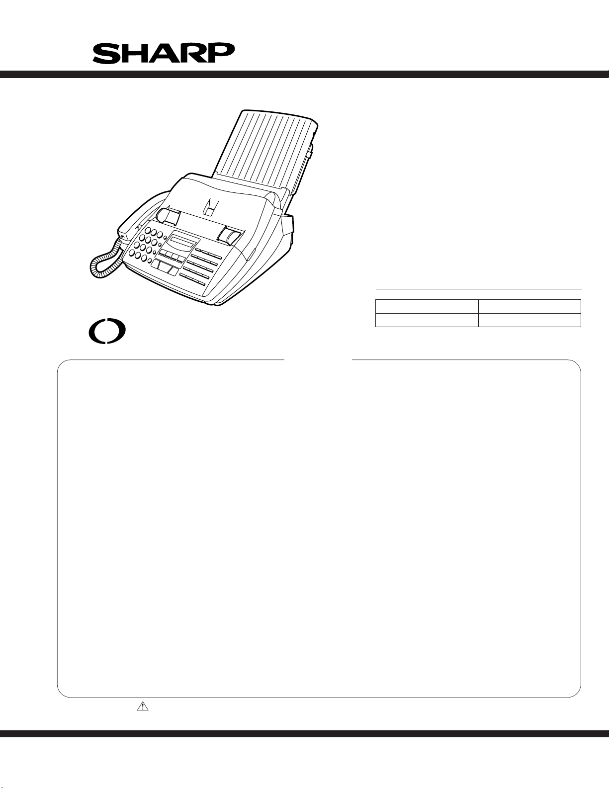
Illustration: UX-510UA
open
LCR
www.OpenLCR.com
CONTENTS
CHAPTER 1. GENERAL DESCRIPTION
[1] Specifications ............................................ 1-1
[2] Operation panel......................................... 1-2
[3] Transmittable documents .......................... 1-3
[4] Installation ................................................. 1-4
[5] Quick reference guide ............................... 1-9
CHAPTER 2. ADJUSTMENTS
[1] Adjustments .............................................. 2-1
[2] Diagnostics and service soft switch .......... 2-2
[3] Troubleshooting ...................................... 2-19
[4] Error code table....................................... 2-20
CHAPTER 3. MECHANISM BLOCKS
[1] General description ................................... 3-1
[2] Disassembly and assembly
procedures ....................................... 3-4
CHAPTER 4. DIAGRAMS
[1] Block diagram ............................................4-1
[2] Wiring diagram .......................................... 4-2
[3] Point-to-point diagram ............................... 4-3
SELECTION CODE DESTINATION
U U.S.A.
CHAPTER 5. CIRCUIT DESCRIPTION
[1] Circuit description ..................................... 5-1
[2] Circuit description of control PWB ............ 5-2
[3] Circuit description of TEL/LIU PWB .......... 5-8
[4] Circuit description of
power supply PWB............................5-11
[5] Circuit description of CCD PWB ..............5-11
CHAPTER 6. CIRCUIT SCHEMATICS AND
PARTS LAYOUT
[1] Control PWB circuit ................................... 6-1
[2] TEL/LIU PWB circuit.................................. 6-9
[3] Power supply PWB circuit ...................... 6-13
[4] CCD PWB circuit..................................... 6-15
[5] Operation panel PWB circuit ................... 6-16
CHAPTER 7. OPERATION FLOWCHART
[1] Protocol ..................................................... 7-1
[2] Power on sequence................................... 7-2
CHAPTER 8. OTHERS
[1] Service tools ............................................. 8-1
[2] IC signal name .......................................... 8-4
[3] Changing the record paper size ................ 8-6
PARTS GUIDE
Parts marked with " " are important for maintaining the safety of the set. Be sure to replace these par ts with specified ones for
maintaining the safety and performance of the set.
This document has been published to be used
SHARP CORPORATION
for after sales service only.
The contents are subject to change without notice.
Page 2

UX-510UA
FO-1470U
CAUTION FOR BATTERY REPLACEMENT
(Danish) ADVARSEL !
Lithiumbatteri-Eksplosionsfare ved fejlagtig håndtering.
Udskiftning må kun ske med batteri af samme fabrikat og type.
Levér det brugte batteri tilbage til leverandoren.
(English) Caution !
Danger of explosion if battery is incorrectly replaced.
Replace only with the same or equivalent type
recommended by the equipment manufacturer.
Discard used batteries according to manufacturer’s
instructions.
(Finnish) VAROITUS
Paristo voi räjähtää, jos se on virheellisesti asennettu.
Vaihda paristo ainoastaan laitevalmistajan suosittelemaan
tyyppiin. Hävitä käytetty paristo valmistajan ohjeiden
mukaisesti.
(French) ATTENTION
Il y a danger d’explosion s’ il y a remplacement incorrect
de la batterie. Remplacer uniquement avec une batterie du
même type ou d’un type recommandé par le constructeur.
Mettre au rébut les batteries usagées conformément aux
instructions du fabricant.
(Swedish) VARNING
Explosionsfare vid felaktigt batteribyte.
Använd samma batterityp eller en ekvivalent
typ som rekommenderas av apparattillverkaren.
Kassera använt batteri enligt fabrikantens
instruktion.
(German) Achtung
Explosionsgefahr bei Verwendung inkorrekter Batterien.
Als Ersatzbatterien dürfen nur Batterien vom gleichen Typ oder
vom Hersteller empfohlene Batterien verwendet werden.
Entsorgung der gebrauchten Batterien nur nach den vom
Hersteller angegebenen Anweisungen.
Page 3

CHAPTER 1. GENERAL DESCRIPTION
[1] Specifications
UX-510UA
FO-1470U
Automatic dialing: Rapid Key Dialing: 36 numbers
Speed Dialing: 63 numbers
Imaging film: Initial starter roll (included with
machine): Approx. 60 letter-size pages
Replacement roll:
UX-15CR/FO-15CR (One roll yields
approx. 500 letter-size pages)
Memory size* : 512 KB (approx. 30 average pages with
ECM turned off)
Modem speed: 14,400 bps with Automatic Fallback to
2400 bps.
Transmission time* : Approx. 6 seconds
Resolution: Horizontal:
203 pels/inch (8 dots/mm)
Vertical:
Standard: 98 lines/inch
(3.85 lines/mm)
Fine/Halftone: 196 lines/inch
(7.7 lines/mm)
Super fine: 391 lines/inch
(15.4 lines/mm)
Automatic document feeder: 20 sheets max.
Recording system: Thermal transfer recording
Halftone (grayscale): 64 levels
Display: 7 x 5 dots, 1 line by 16-digit display
Paper tray capacity: Letter: 200 sheets
(16-to 20-lb. paper) Legal: 200 sheets
Compression scheme: MH, MR, MMR
Applicable telephone line: Public switched telephone network
Compatibility: ITU-T (CCITT) G3 mode
Input document size: Automatic feeding:
Width 5.83 to 8.5"
(148 to 216 mm)
Length 5.04 to 11"
(128 to 279 mm)
Manual feeding:
Width 5.83 to 8.5"
(148 to 216 mm)
Length 5.04 to 39.4"
(128 to 1000 mm)
Effective scanning width: 8.2" (208 mm) max.
Effective printing width: 8.1" (206 mm) max.
Contrast control: Automatic/Dark selectable
Reception modes: TEL/FAX/A.M. (Note: A.M. mode is for
connecting an answering machine)
Copy function: Single/Multi/Sort (99 copies/page)
Telephone function: Yes
(cannot be used if power fails)
Power requirements: 120 V AC, 60 Hz
Operating temperature: 41 to 95°F (5 to 35°C)
Humidity: Maximum: 80 % RH
Power consumption: Stand-by: 3.6 W
Maximum: 100 W
Dimensions: Width: 14.4" (365 mm)
Depth: 19.0" (482 mm)
(With attachments)
Height: 10.6" (270 mm)
(With attachments)
Weight: Approx. 10.6 lbs. (4.8 kg)
* Based on ITU-T (CCITT) Test Chart #1 at standard resolution in Sharp
special mode, excluding time for protocol signals (i.e., ITU-T phase C
time only).
As a part of our policy of continuous improvement, SHARP reserves the right to make design and specification changes for product
improvement without prior notice. The performance specifications figures indicated are nominal values of production units. There may be some
deviation from these values in individual units.
1 – 1
Page 4
UX-510UA
FO-1470U
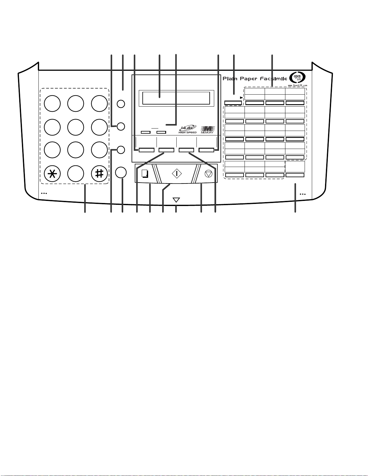
[2] Operation panel
ABC DEF
123
GHI JKL MNO
456
TUV WXYZPQRS
789
0
18
SPEED
DIAL
REDIAL
HOLD/
SEARCH
SPEAKER
16
VOLUME
DOWN
RECEPTION
MODE
COPY/
HELP
UP
FUNCTION
START
PANEL RELEASE
121415
1317
TEL FAX
RESOLUTION
11
A.M.
MEMORY
STOP
10
7
SHIFT
81 4 5 62 3
01 02 03
19 20 21
0504 06 07
2322 24 25
0908 10 11
2726 28 29
1312 14/POLL 15/P1
3130 32 33
17/G116/P2 18/G2
3534 36
OpenLCR
OpenLCR
9
1. REDIAL key
Press this key to automatically redial the last number dialed.
2. SPEED DIAL key
Press this key to dial a fax or voice number using an
abbreviated 2-digit Speed Dial number.
3. RECEPTION MODE key
Press this key to select the mode of reception.
4. Display
This displays messages and prompts during operation and
programming.
5. VOLUME keys
Press these keys to adjust the volume of the speaker when
@
the
handset when the handset is lifted, or the volume of the
ringer at all other times.
SPEAKER key has been pressed, the volume of the
6. MEMORY key
Press this key to scan a document into memory before
transmitting it.
7. SHIFT key
Press this key before pressing the Rapid key.
8. Rapid Dial keys
Press one of these keys to dial a fax number automatically.
9. Open LCR key
Press this key to register for Open LCR service and
receive carrier rate data to your fax.
10. RESOLUTION key
Press this key to adjust the resolution for faxing or copying.
11. STOP key
Press this key to cancel an operations before they are
completed.
12. Panel release
Grasp this finger hold and pull toward you to open the operation
panel.
13. START key
Press this key to begin transmission when using Speed
Dialing, Direct Keypad Dialing, or Normal Dialing.
14. COPY/HELP key
When a document is in the feeder, press this key to make
a copy of a document. At any other time, press this key to
print out the Help List, a quick reference guide to the
opeation of your fax machine.
15. FUNCTION key
Press this key to select various special functions.
16. SPEAKER key
Press this key to listen to the line and fax tones through
the speaker when faxing a document.
Note: This is not a speakerphone. You must pick up the
handset to talk with the other party.
17. HOLD/SEARCH key
Press this key to search for an auto-dial number, or,
during a phone conversation, press this key to put the
other party on hold.
18. Number keys
Use these keys to dial numbers, and enter numbers and letters
when storing auto-dial numbers.
1 – 2
Page 5
[3] T ransmittable documents
[
]
[
]
0.2"(5mm)
0.2"(5mm)
Readable length
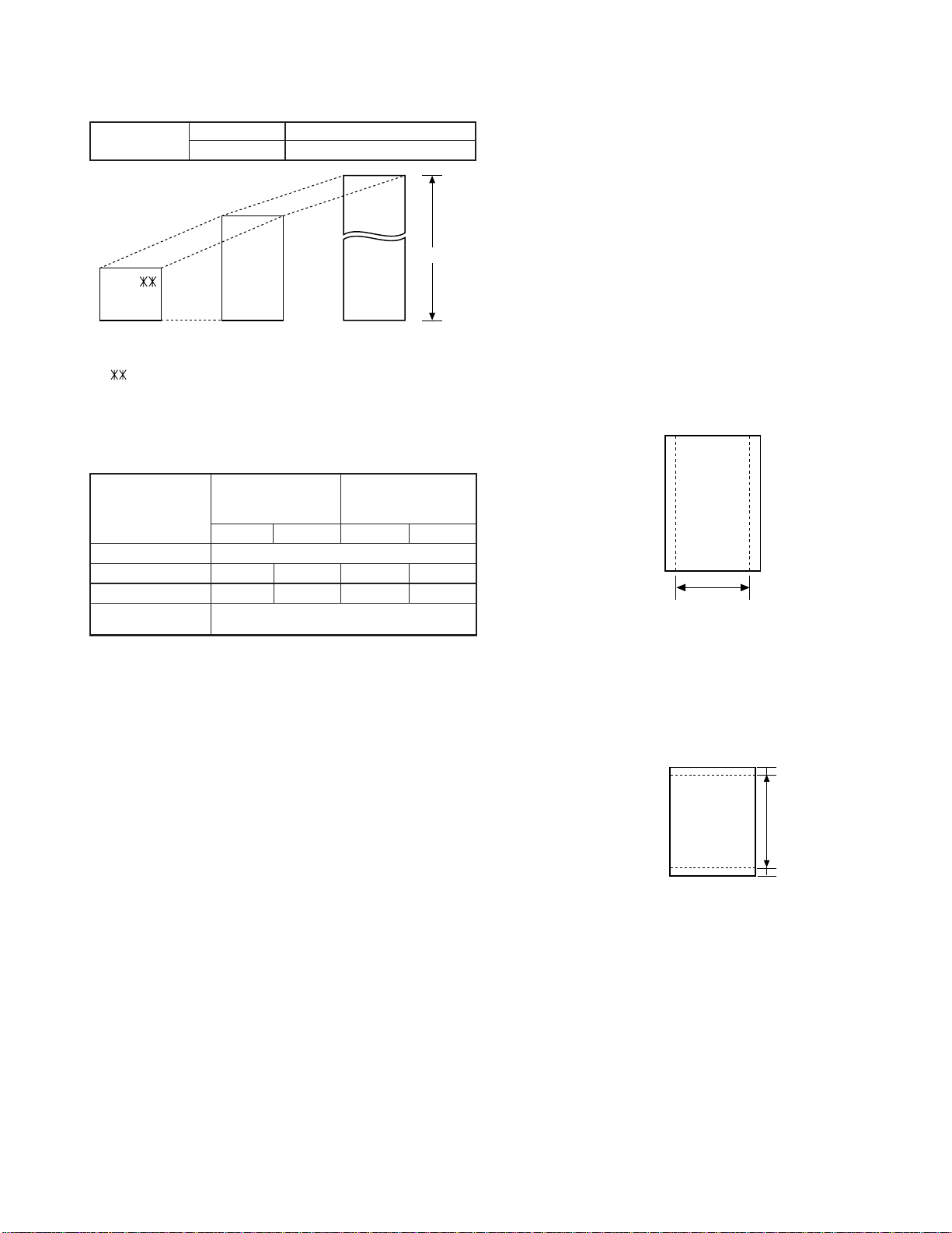
1. Document Sizes
Normal size
(Min.)
128mm
148mm 216mm
Use document carrier sheet for smaller documents.
* With special sizes, only one sheet can be fed into the machine at a
time. Insert next page into feeder as current page is being scanned.
2. Paper Thickness & Weight
width 5.83" – 8.5"(148 – 216 mm)
length 5.04" – 11"(128 – 279 mm)
(Max.)
(Max.)
Letter
size
Normal size
279mm
216mm
Special size
1000mm
UX-510UA
FO-1470U
5. Automatic Document Feeder Capacity
Number of pages that can be placed into the feeder at anytime is as
follows:
Normal size: max. ADF 20 sheets
Special size: single sheet only (manual feed)
NOTES: • When you need to send or copy more pages than the feeder
limit, place additional pages in feeder when last page in
feeder is being scanned.
• Place additional pages carefully and gently in feeder.
If force is used, double-feeding or a document jam may
result.
6. Readable Width & Length
The readable width and length of a document are slightly smaller than
the actual document size.
Note that characters or graphics outside the effective document scanning range will not be read.
• Readable width
8.1" (206mm), max.
4x6 series
(788mm x 1091mm x
1000 sheets)
Minimum Maximum Minimum Maximum
Feeder capacity 20 sheets, max.
Paper weight 45kg 64.3kg 52g/m274.3g/m
Paper thickness (ref.)
Paper size 128mm x 148mm ~ (MIN. SIZE)
0.06mm 0.09mm 0.06mm 0.09mm
A4 (210mm x 297mm), Letter (216mm x 279mm)
Square
meter series
3. Document Types
• Normal paper
Documents handwritten in pencil (No. 2 lead or softer), fountain
pen, ball-point pen, or felt-tipped pen can be transmitted.
Documents of normal contrast duplicated by a copying machine
can also be transmitted.
• Diazo copy (blue print)
Diazo copy documents of a normal contrast may be transmitted.
• Carbon copy
A carbon copy may be transmitted if its contrast is normal.
4. Cautions on Transmitting Documents
• Documents written in yellow, greenish y ellow, or light b lue ink cannot
be transmitted.
• Ink, glue, and correcting fluid on documents must be dry before
the documents can be transmitted.
• All clips, staples and pins must be removed from documents before transmission.
• Patched (taped) documents should be copied first on a copier and
then the copies used for transmission.
• All documents should be fanned before insertion into the feeder to
prevent possible double feeds.
2
Readable width
• Readable length
This is the length of the document sent minus 0.2" (5mm) from the top
and bottom edges.
1 – 3
Page 6
UX-510UA
FO-1470U
7. Use of Document Carrier Sheet
A document carrier sheet must be used for the following documents.
• Those with tears.
• Those smaller than siz e 5.83" (W) x 5.04" (L) (148 mm (W) x 128 mm
(L)).
• Carbon-backed documents
TELEPHONE JACK
A standard RJ11C telephone jack must be located near the machine.
This is the telephone jack commonly used in most homes and offices.
• Plugging the fax machine into a jack which is not a RJ11C jack may
result in damage to the machine or your telephone system. If y ou do
not know what kind of jack you hav e, or needed to hav e one installed,
contact the telephone company.
Make print straight
across paper
E.G.
Place the document
carrier in the document
feeder with the clear film
side down
Direction of insertion
NOTE: To transmit a carbon-backed document, insert a white sheet of
paper between the carbon back of the document and the document carrier.
• Those containing an easily separ able writing substance (e.g., track-
ing paper written on with a soft, heavy lead pencil).
NOTES: • When using the document carrier, carefully read the in-
structions written on the back.
• If the document carrier is dirty, clean it with a soft, moist
cloth, and then dry it before using for transmission.
• Do not place more than one document in the carrier at a
time.
[4] Installation
1. Site selection
T ak e the follo wing points into consideration when selecting a site for this
model.
ENVIRONMENT
• The machine must be installed on a level surface.
2. Loading the imaging film (UX-15CR/FO-15CR)
Your fax uses a roll of imaging film to create printed text and images.
The print head in the fax applies heat to the imaging film to transfer ink to
the paper. Follow the steps below to load or replace the film.
• The initial starter roll of imaging film included with your fax can print
about 60 letter-size pages.
• When replacing the film, use a roll of Sharp UX-15CR/FO-15CR
imaging film. One roll can print about 500 letter-size pages.
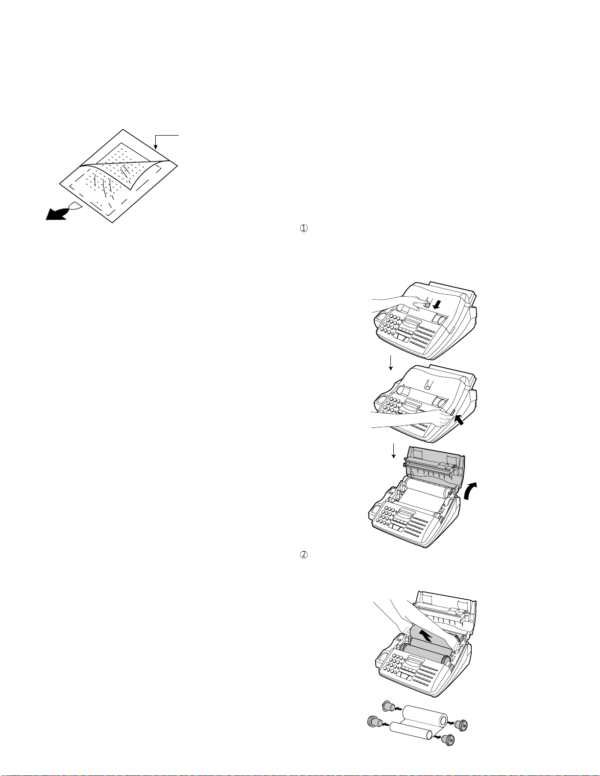
1
Press the release marked OPEN and open the print compartment
cover.
• Caution! The printing head (the strip of metal on the underside of
the cover) applies heat to the printing film. It may be hot
if a document has just been printed.
• Keep the machine away from air conditioners, heaters, direct sun-
light, and dust.
• Provide easy access to the front, back, and sides of the machine. In
particular, keep the area in front of the machine clear , or the original
document may jam as it comes out after scanning.
• The temperature should be between 5° and 35°C.
• The humidity should be between 30% and 85% (without conden-
sation).
ELECTRICITY
AC 120V, 60Hz, grounded (3-prong) AC outlet is required.
Caution!
• Connection to a power source other than that specified will cause
damage to the equipment and is not covered under the warranty.
• If y our area experiences a high incidence of lightning or power surges,
we recommend that you install a surge protector for the power and
telephone lines. Surge protectors can be purchased at most telephone
speciality stores.
If the machine is moved from a cold to a warm place...
Condensation may form on the reading glass if machine is moved from
a cold to a warm place, this will prevent proper scanning of documents
for transmission. Turn on the power and wait approximately 2 hours before using machine.
1 – 4
2
If you are replacing the imaging film, take the old film out of the printing compartment and remove the three (3) green gears and the green
flange from the ends of the spools.
DO NOT DISCARD THE GREEN GEARS AND THE GREEN
FLANGE!
Page 7
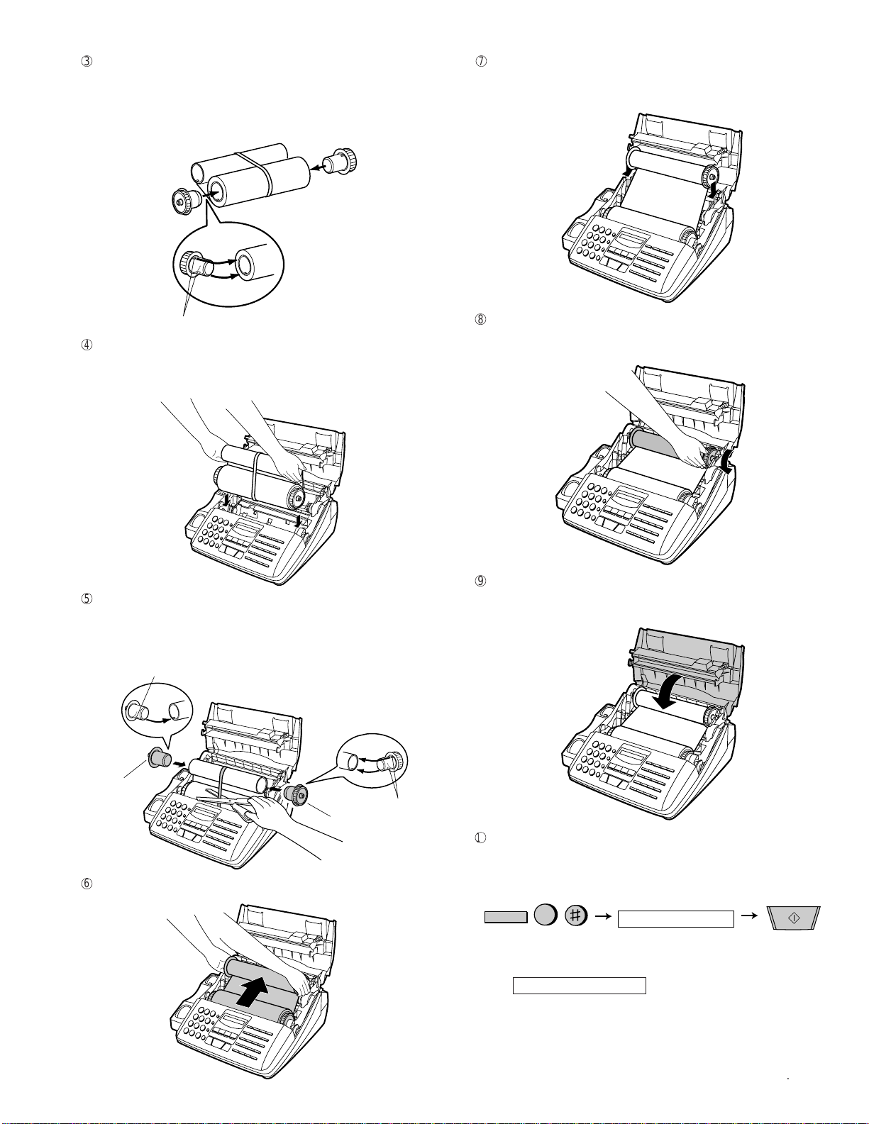
3
FUNCTION
START
6
INITIALIZE FILM
Display shows:
Take the new film out of its package, and insert two of the gears
provided with the fax into the ends of the spool with film. Make sure
that the two tabs on the gears fit properly into the slots in the ends of
the spool.
• Do not yet remove the band which holds the spools together.
2 tabs
4
Hold the empty spool so that the end with only one slot is on the left,
and lower the spools into the front of the printing compartment. The
gears in the ends of the spool with film should fit into the slots on
each side of the printing compartment.
UX-510UA
FO-1470U
7
Insert the empty spool into the back of the compartment so that the
gear and the flange fit into the slots on the sides of the compartment.
• Make sure that the gear engages with the gear below it.
8
Wind the film slightly (rotate the gear on the right side of the empty
spool) so that there is no slack in the film. Make sure that both edges
of the film wind onto the spool evenly.
5
Cut the band which holds the spools together with scissors, and re-
move it. Inser t the remaining gear into the right end of the empty
spool and the flange into the left end of the empty spool. Make sure
the tabs on the gear and the flange fit into the slots in the ends of the
spool (the gear has two tabs and the flange has one tab).
1 tab
Flange
Gear
6
Pull the empty spool toward the back of the compartment, unwind-
ing the film as you pull.
2 tabs
9
Close the print compartment cover, making sure it clicks into place.
• Caution! Close the cov er slowly to make sure it doesn’t pinch your
fingers.
F
Load paper in the paper tray and then press the following keys to
initialize the film.
Note: Paper must be loaded before the film can be initialized. To load
paper, see Loading the Printing Paper.
When to replace the imaging film
Replace the imaging film when the display shows:
FILM END
Use the following imaging film, which is av ailable from y our dealer
or retailer: Sharp UX-15CR/FO-15CR Imaging Film
• Caution! The text of documents printed with the imaging film is
visible on the used film. If confidential information has
been printed, dispose of the film appropriately.
1 – 5
Page 8
UX-510UA
FO-1470U
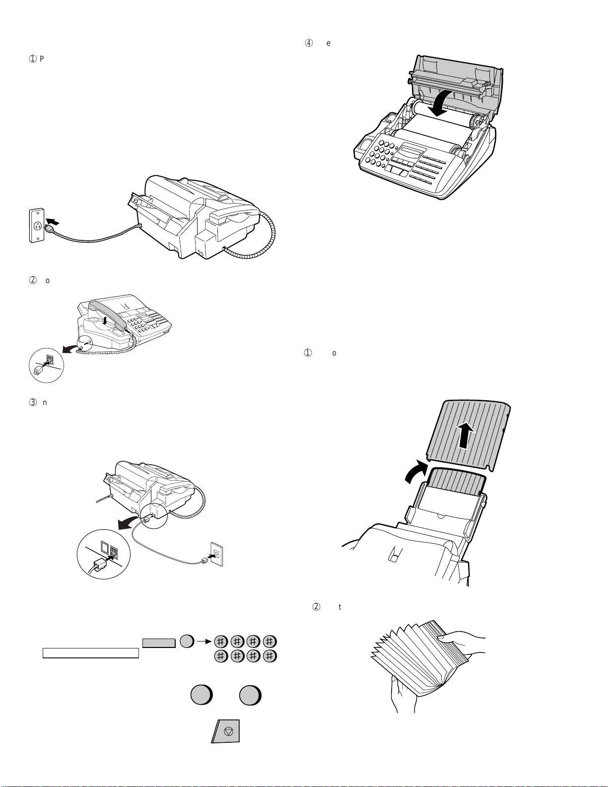
3. Assembly and connections
1
Plug the power cord into a 120V, 60Hz, grounded(3-prong) outlet.
• Caution: Do not plug the power cord into any other kind of outlet.
This will damage the machine and is not covered under the
warranty.
• The machine does not have a power on/off switch, so the power
is turned on and off by simply plugging in or unplugging the power
cord.
Note: If your area experiences a high incidence of lightning or power
surges, we recommend that you install surge protectors for
the power and telephone lines. Surge protectors can be
purchased at most telephone specialty stores.
2
Connect the handset as shown and place it on the handset rest.
Make sure the handset cord
goes into the unmarked jack
on the side of the machine!
Use the handset to make ordinary
phone calls, or to transmit and receive
faxes manually.
4
Insert the paper tray into the back of the fax as shown.
4. Loading printing paper
The paper tray holds the paper on which received documents and
copies are printed. Up to 200 sheets of letter or legal paper from
16 to 20 lbs. (60 to 75 g/m2) can be loaded in the tray. Less sheets can
be loaded when using heavier paper. The maximum allowed paper
weight is 24 lbs. (90 g/m2).
Note: When receiving or copying documents, do not allow more than
100 pages to collect in the received documents outlet. Otherwise ,
the outlet may become obstructed, causing paper jams.
• Caution! Do not use the blank side of paper that has already been
1
Remove the paper cover if it is on the paper tray.
• If you are going to load legal size paper, flip up the paper tray
extender.
printed on.
3
Insert one end of the line cord into the jack on the back of the ma-
chine marked TEL.LINE. Insert the other end into a standard (RJ11C)
single-line wall telephone jack.
Be sure to insert the line into the TEL.LINE jack.
Do not insert into the TEL.SET jack.
TEL.
SET
TEL.
LINE
Note: The fax machine is set for tone dialing. If you are on a pulse
dial line, you must set the fax machine for pulse dialing.
Press the keys on the operation panel as follows:
1. Press these keys:
The display will show:
DIAL MODE
2. Press 1 to select tone dialing, or 2
to select pulse dialing.
3. Press the STOP key to return to the date
and time display.
FUNCTION
4
TONE
1
or
STOP
PULSE
2
2
Fan the paper, and then tap the edge against a flat surf ace to e ven
the stack.
1 – 6
Page 9
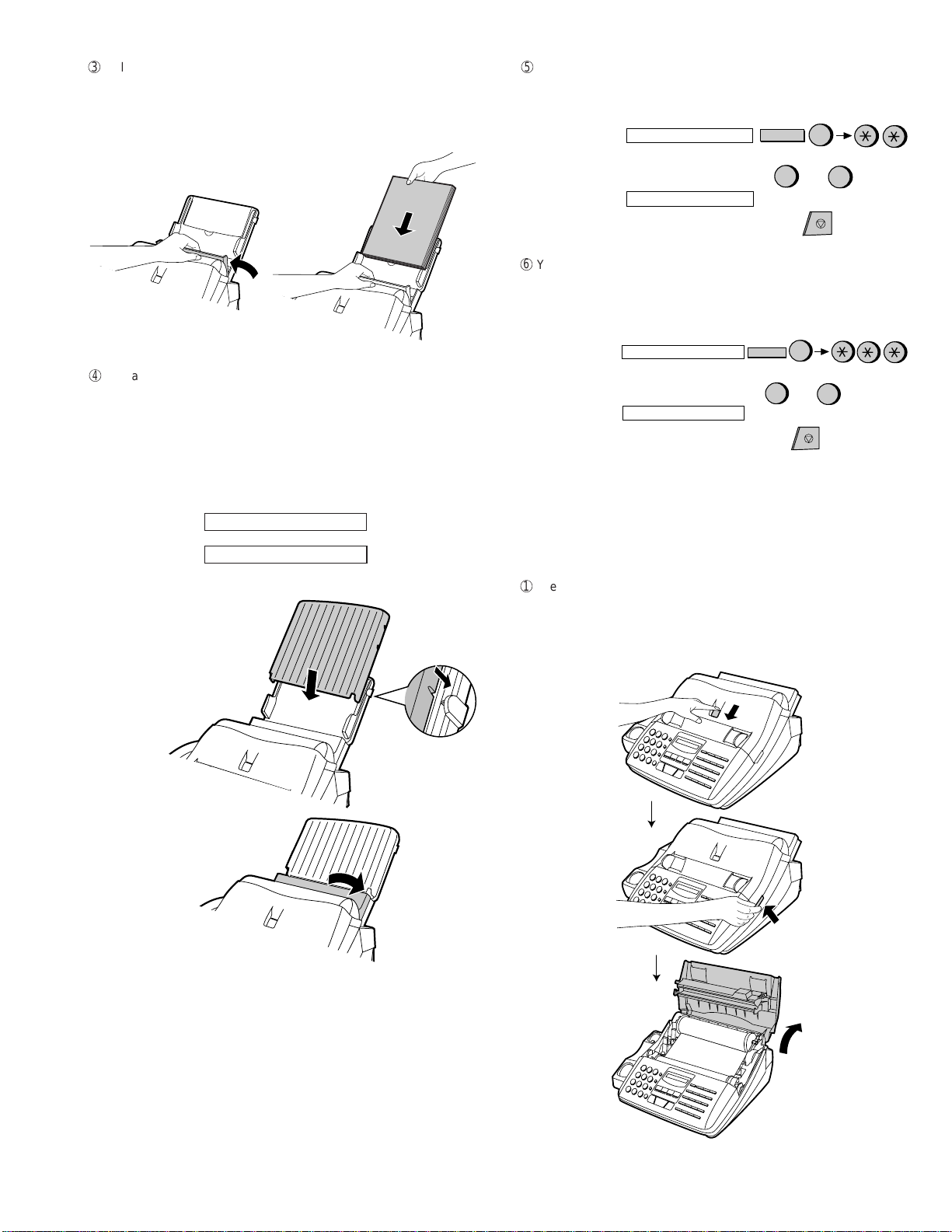
3
Pull the paper release plate toward you and insert the stack of paper
into the tray, print side down.
• If paper remains in the tray, take it out and combine it into a single
stack with the new paper before adding the new paper.
4
Replace the paper cover on the paper tray.
• Important: Be sure to replace the paper cover before you put
back the paper release plate down.
Note: If the display shows the following alternating messages when
making a copy or receiving a fax, check the paper tray. If the tray is
empty, add paper and then press the START key. If there is paper,
make sure it is inserted correctly and then press the START key.
SET PAPER &
PRESS START KEY
↑
↑
UX-510UA
FO-1470U
5
The fax has been set at the f actory to scale the size of received f axes
to letter size paper. If you have loaded legal paper , you m ust change
the paper size setting to legal. Press these keys:
The display will show: PAPER SIZE SET
Press 1 to select LETTER, 2 to select LEAGAL.
The display will show: COPY CUT-OFF
Press the STOP key to return to the date and time display.
6
Your fax has been set at the factory to print at normal contrast.
FUNCTION
LETTER
1
6
LEAGAL
or
STOP
2
Depending on the type of paper you have loaded, you may find that
you obtain better print quality by changing the setting to LIGHT.
Press these keys:
The display will show: PRINT CONTRAST
Press 1 to select NORMAL or 2 to select LIGHT.
The display will show: PAPER SIZE SET
Press the STOP key to return to the date and time display.
FUNCTION
NORMAL
1
6
LIGHT
2
or
STOP
5. Clearing paper jams
If a document doesn’t feed properly during transmission or copying, or
DOCUMENT JAMMED appears in the display, first try pressing the
START key. If the document doesn’t feed out, open the operation panel
(grasp the front edge at the "PANEL RELEASE" mark and pull up) and
pull it out gently.
1
Press the release marked OPEN and open the pr int compartment
cover.
• Caution! The printing head (the strip of metal on the underside of
the frame) applies heat to the imaging film. It may be hot
if a document has just been printed.
1 – 7
Page 10
UX-510UA
FO-1470U
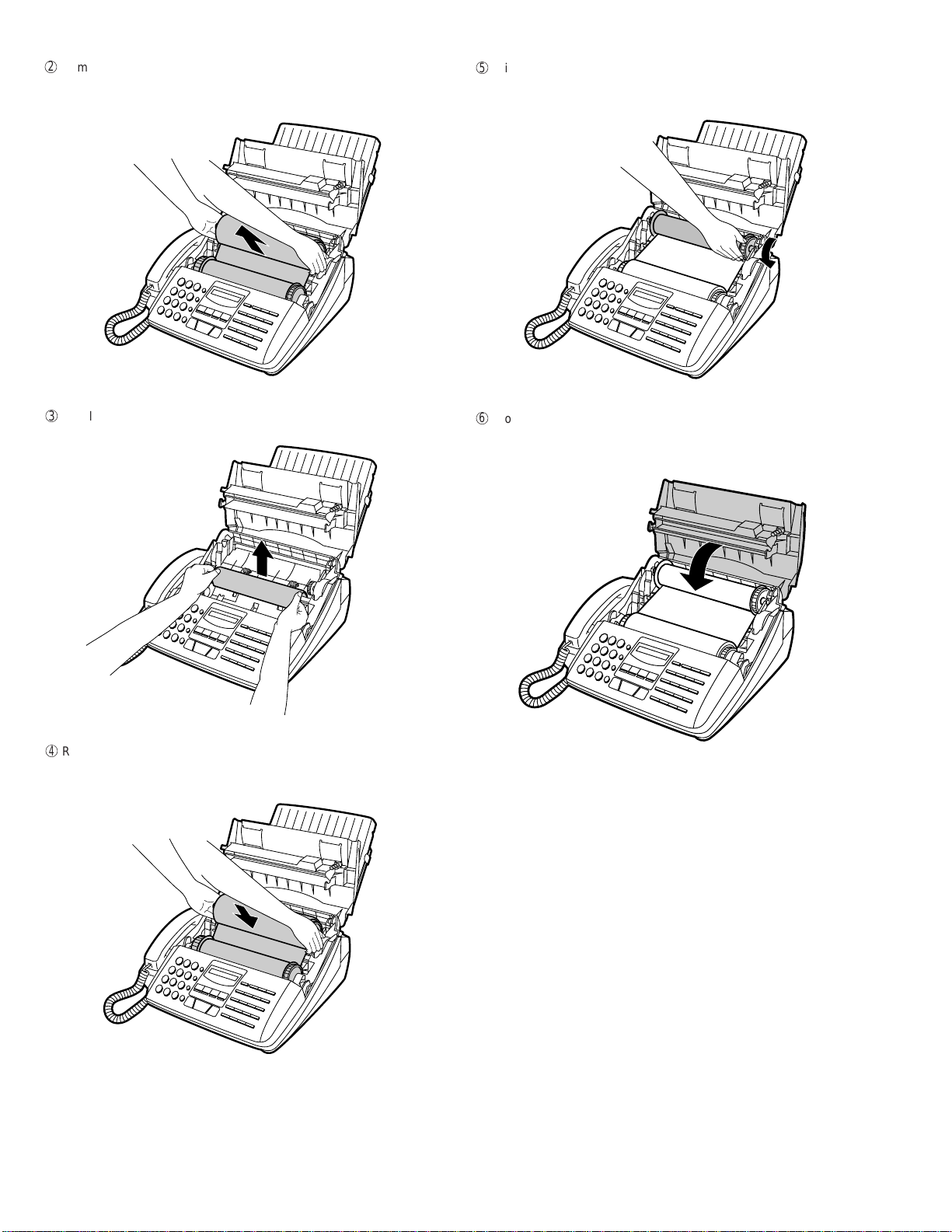
2
Remove the imaging film from the printing compartment and set it on
a sheet of paper.
3
Gently pull the jammed paper out of the printing compartment.
5
Wind the film slightly (rotate the gear on the right side of the rear
spool) so that there is no slack in the film. Make sure that both edges
of the film wind onto the spool evenly.
6
Close the print compartment cover, making sure it clicks into place.
• Caution! Close the co ver slowly to mak e sure it doesn’t pinch your
fingers.
4
Replace the imaging film, making sure that the flange goes into the
rear slot on the left side of the printing compartment. Also, make sure
that the right, rear gear engages with the gear below it.
1 – 8
Page 11
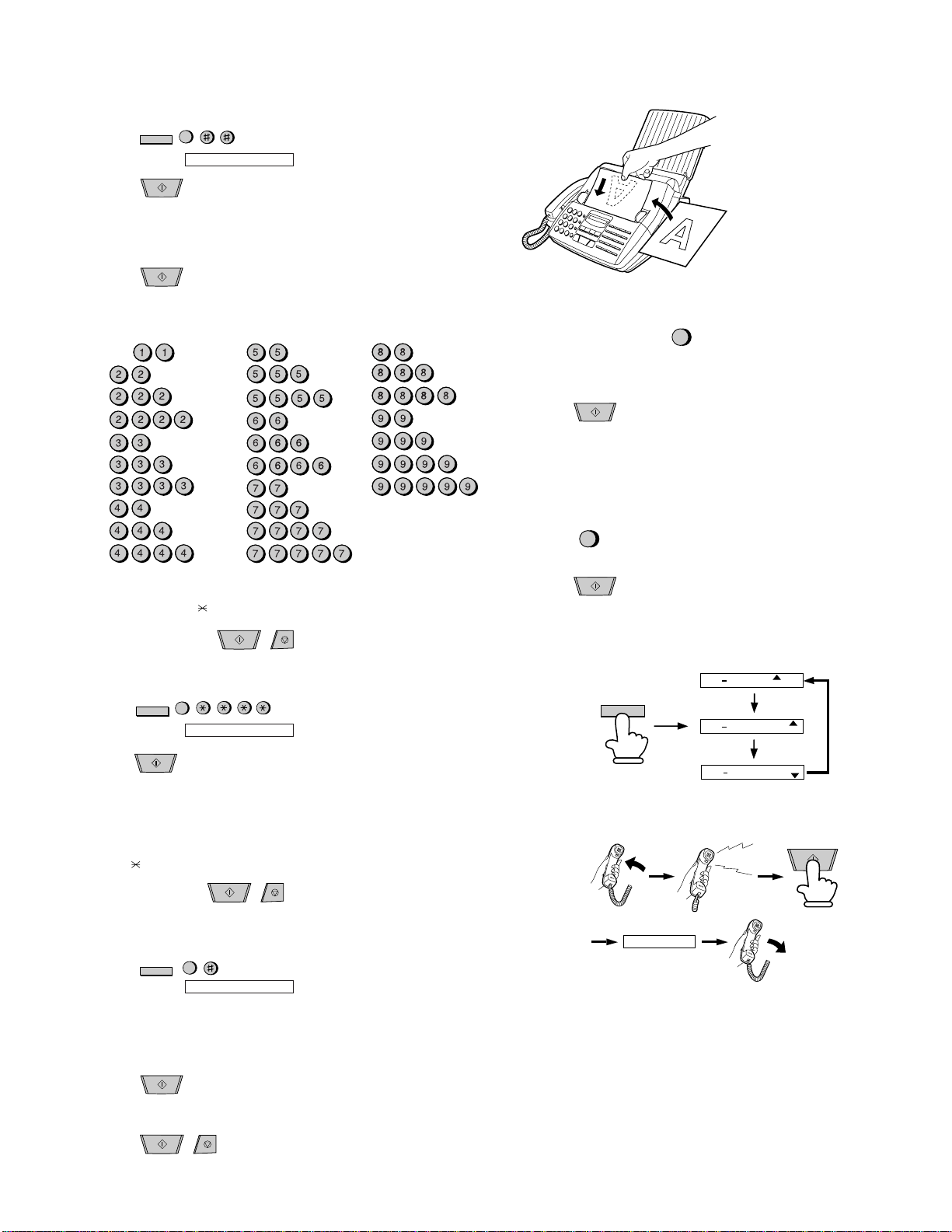
[5] Quick reference guide
3
FUNCTION
3
FUNCTION
ENTERING YOUR NAME AND NUMBER
1. Press:
Display shows: OWN NUMBER SET
2. Press:
3. Enter your fax number (max. of 20 digits) by pressing the number keys.
♦ To insert a space between digits, press the # key.
♦ If you mak e a mistake , press the SPEED DIAL ke y to backspace and clear the
4. Press:
5. Enter your name by pressing the appropriate number keys as shown below.
♦ To enter two letters in succession that require the same key , press the SPEAKER
SPACE =
A =
B =
C =
D =
E =
F =
G =
H =
I =
• To change case, press the REDIAL key.
6. When finished, press:
SETTING THE DATE AND TIME
1. Press:
2. Press:
3. Enter two digits for the month (01 to 12).
4. Enter two digits for the day (01 to 31).
5. Enter four digits for the year (Ex: 2000).
6. Enter two digits for the hour (01 to 12)
and two digits for the minute (00 to 59).
7. Press
8. When finished, press:
START
mistake.
START
key after entering the first letter.
J =
K =
L =
M =
N =
O =
P =
Q =
R =
S =
Press # or
to scroll through symbols and special characters.
START
Display shows: DATE & TIME SET
START
for A.M. or # for P.M.
START
T =
U =
V =
W =
X =
Y =
Z =
STOP
STOP
UX-510UA
FO-1470U
SENDING FAXES
Place your document (up to 20 pages)
face down in the document feeder.
Normal Dialing
1. Lift the handset or press:
2. Dial the fax number.
3. Wait for the reception tone (if a person answers, ask them to press their Start
key).
4. Press:
START
Rapid Key Dialing
Press the appropriate Rapid Key (if the Rapid Key is from 19 to 36, press the
SHIFT key first).
Transmission will begin automatically.
Speed Dialing
SPEED
1. Press:
DIAL
2. Enter 2-digit Speed Dial number.
3. Press:
START
RECEIVING FAXES
Press the RECEPTION MODE key until the appears in the display points to the
desired reception mode.
RECEPTION
MODE
FAX mode: The fax machine automatically ans wers on f our rings and receives the
incoming document.
TEL mode:
SPEAKER
NOV 05 10:30
NOV 05 10:30
NOV 05 10:30
Beep
FAX
TEL
A.M.
FAX
TEL
A.M.
FAX
TEL
A.M.
START
STORING AND CLEARING AUTO DIAL NUMBERS
1. Press:
2. Press 1 to store a number or 2 to clear a number.
3. Enter a 2-digit number (from
4. Enter the full fax/telephone number.
5. Press:
6. Enter the name of the location by pressing number keys (Refer to the letter
7. Press:
FUNCTION
3
Display shows: FAX/TEL # MODE
"01" to "99") by pressing the number keys. This
will be the Speed Dial number. (If you are clearing a number, go to Step 7.)
START
entry table in
ENTERING YOUR NAME AND NUMBER
START
STOP
RECEIVING
A.M. mode: Select this mode when an answering machine is connected to the f ax
and the answering machine is turned on.
.)
1 – 9
Page 12

UX-510UA
FO-1470U
M E M O
1 – 10
Page 13
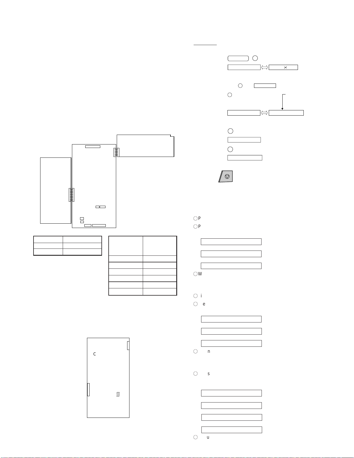
CHAPTER 2. ADJUSTMENTS
[1] Adjustments
General
Since the following adjustments and settings are provided f or this model,
make adjustments and/or setup as necessary.
1. Adjustments
Adjustments of output voltage (FACTORY ONLY)
1. Install the power supply unit in the machine.
2. Set the recording paper and document.
3. When the document is loaded, power is supplied to the output lines.
Confirm that outputs are within the limits below.
Output voltage settings
POWER
SUPPLY
PWB
TEL/LIU
PWB
CNTH
CONTROL
PWB
CNPW
3. Settings
(1) Dial mode selector
DIAL mode (Soft Switch No. SWB4 DATA No. 3)
(step 1) Select "OPTION SETTING".
KEY : FUNCTION 4
DISPLAY: OPTION SETTING PRESS OR #
(step 2) Select "DIAL MODE".
KEY: Push # until " DIAL MODE " is
indicated because the number of
# s changes by the model.
DISPLAY: DIAL MODE
(step 3) Select, using "1" or "2".
KEY: 1
DISPLAY: TONE SELECTED
KEY: 2
DISPLAY: PULSE SELECTED
(step 4) End, using the "STOP" key.
KEY:
STOP
1=TONE, 2=PULSE
UX-510UA
FO-1470U
Cursor
When initially registering,
the mode shows 1=TONE.
When registering again, the
mode which was registered
formerly is shown.
CNLIUACNLIUA
CNLED
CNSP
CNCSW
CNCCD
Output Voltage limits
+5V 4.75V ∼ 5.25V
+24V 23.3V ∼ 24.7V
CNMT
CNPN
Connector
No. CNPW
Pin No.
1 +24V
2 +24V
3MG
4MG
5 +5V
6DG
2. IC protectors replacement
ICPs (IC Protectors) are installed to protect the motor driver circuit.
ICPs protect various ICs and electronic circuits from an overcurrent condition.
The location of ICPs are shown below:
CONTROL
PWB (TOP SIDE)
CNLIUA
(1)FU100 (KAB2402) is installed in order to protect IC’s from an over-
current generated in the motor drive circuit. If FU100 is open, replace
it with a new one.
FU100
4. V olume adjustment
You can adjust the volume of the speaker and ringer using the UP and
DOWN keys.
(1) Speaker
1
Press the SPEAKER key.
2
Press the UP or DOWN key.
Display:
SPEAKER: HIGH
↔
SPEAKER: MIDDLE
↔↔
SPEAKER: LOW
3
When the display shows the desired volume le vel, press the SPEAKER
key to turn off the speaker.
(2) Handset
1
Lift the handset.
2
Press the UP or DOWN key.
Display:
RECEIVER: HIGH
RECEIVER: MIDDLE
↔
RECEIVER: LOW
3
When the display shows the desired volume level, replace the handset.
(3) Ringer
1
Press the UP or DOWN key. (Make sure the SPEAKER key has not
been pressed and the handset is not lifted.)
Display:
RINGER: HIGH
↔
RINGER: MIDDLE
↔
RINGER: LOW
↔
RINGER OFF: OK?
2
If you selected RINGER OFF: OK?, press the START key.
The ringer will ring once
at the selected level, then
the date and time will reappear in the display.
2 – 1
Page 14
UX-510UA
FO-1470U
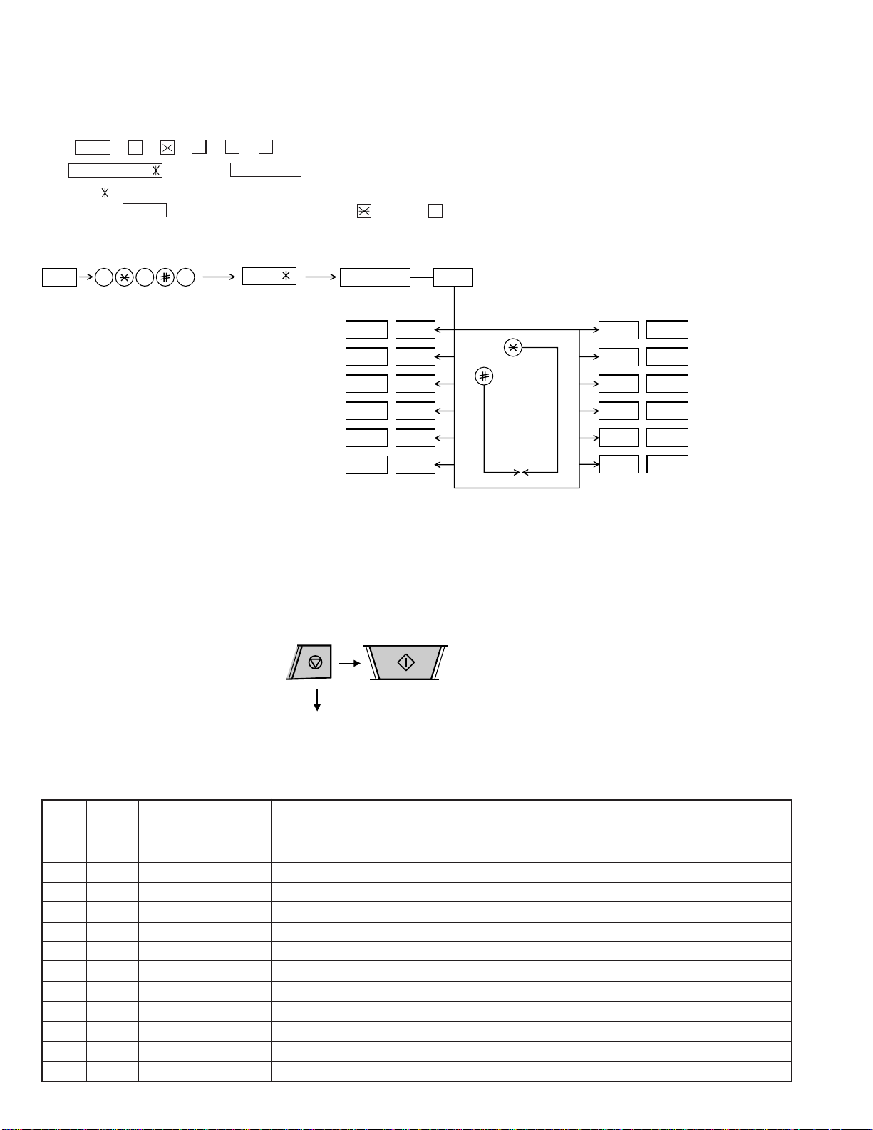
[2] Diagnostics and service soft switch
1. Operating procedure
(1) Entering the diagnostic mode
Press FUNC → 9 → → 8 → # → 7 , and the following display will appear.
ROM Ver. FPS0 After 2 sec: DIAG MODE
FPS0
Then press the START key. Select the desired item with the key or the # key or select with the rapid key. Enter the mode with the START key.
(Diag•specifications)
FUNC
9 8 7
FPS0
DIAG MODE
START 1Soft switch mode
START
START
START
START
START 6Signal send mode
If the diag mode cannot be set, repeat the diag mode operation, performing the following operation.
After the power is turned on and "WAIT A MOMENT" is indicated, press
the STOP key.
STOP
KEY
"Power ON"
+
Memory clear
(Work + Backup)
2ROM & RAM check
3Aging mode
4Panel key test
5Check pattern
START
KEY
START
12
11
10
9
8
7
In relation with the process response (request from Production
Engineering) "WAIT A MOMENT" clock indication ma y appear depending on STOP key timing. If the STOP key is held down,
"MEMORY CLEAR?" appears.
START
START
START
START
START
START
Entry data receive
Entry data send
Auto feeder mode
All black mode
CCD adjust mode
Memory clear
2. Diagnostic items
ITEM DIRECT
No. key
1 1 SOFT SWITCH MODE Soft switches are displayed and changed. List can be output.
2 2 ROM & RAM CHECK ROM is sum-checked, and RAM is matched. Result list is output.
3 3 AGING MODE 10 sheets of check patterns are output every 5 minutes per sheet.
4 4 PANEL KEY TEST Panel keys are tested. Result list is output.
5 5 CHECK PATTERN Check pattern is output.
6 6 SIGNAL SEND MODE Various signals of FAX communication are output.
7 7 MEMORY CLEAR Back-up memory is cleared, and is set at delivery.
8 8 CCD ADJUST MODE Optical system is adjusted.
9 9 ALL BLACK PRINT To check the print head, whole dots are printed over the interval of 2 m.
10 10 AUTO FEEDER MODE Insertion and discharge of document are tested.
11 11 ENTRY DATA SEND Registered content is sent.
12 12 ENTRY DATA RECEIVE Registered content is received, and its list is output.
Contents Function
2 – 2
Page 15
3. Diagnostic items description
3. 1. Soft switch mode
Used to change the soft switch settings.
The soft switch which is stored internally is set by using the keys.
The available soft switches are SW-A1 to SW-N3.
The content of soft switches is shown in page 2-5 to 2-18.
The contents are set to factory default settings.
3. 2. ROM & RAM check
ROM executes the sum check, and RAM executes the matching test.
The result will be notified with the number of short sounds of the buzzer
as well as by printing the ROM & RAM check list.
Number of short sounds of buzzer 0 → No error
1 → ROM error
2 → RAM error (32Kbyte)
3. 3. Aging mode
If any document is first present, copying will be ex ecuted sheet by sheet.
If no document is present, the check pattern will be printed sheet by
sheet. This operation will be executed at a rate of one sheet per 5minutes, and will be ended at a total of 10 sheets.
UX-510UA
FO-1470U
3. 6. Signal send mode
This mode is used to send various signals to the circuit during F AX communication. Ever y push of START key sends a signal in the following
sequence. Moreover , the signal sound is also output to the speaker when
the line monitor of the soft switch is on.
[1] No signals (CML ON)
[2] 14400BPS (V.33)
[3] 12000BPS (V.33)
[4] 14400BPS (V.17)
[5] 12000BPS (V.17)
[6] 9600BPS (V.17)
[7] 7200BPS (V.17)
[8] 9600BPS (V.29)
[9] 7200BPS (V.29)
[10] 4800BPS (V27ter)
[11] 2400BPS (V27ter)
[12] FLAG
[13] 2100Hz
[14] 1100Hz
3. 4. Panel key test
This mode is used to check whether each key operates properly or not.
Press the key on the operation panel, and the key will be displayed on
the display . Theref ore, press all ke ys. At this time, finally press the ST OP
key .
When the STOP key is pressed, the keys which are not judged as
"pressed" will be printed on the result list.
• LED part of the contact image sensor (CIS) is kept on during the term
from when "ST AR T" of the panel test mode to end with the STOP k ey .
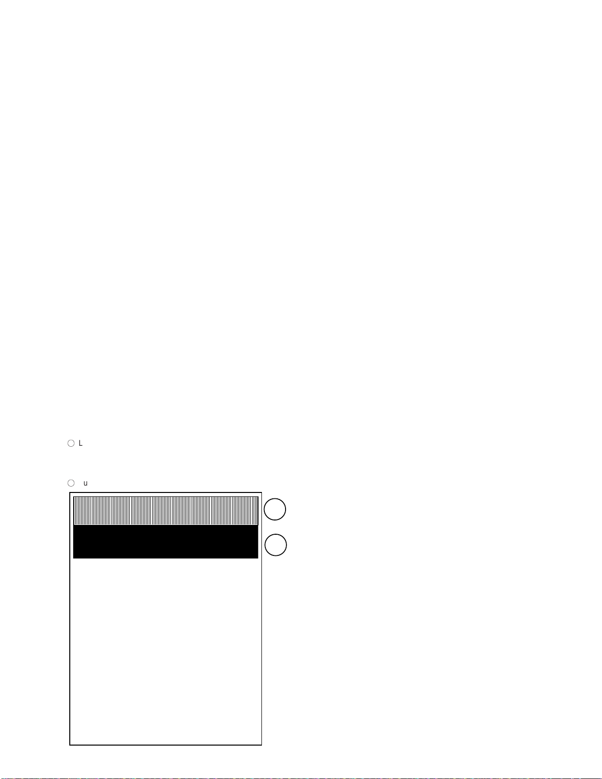
3. 5. Check pattern
This mode is used to check the state of the printing head. It is ended
with the following pattern printed on one printing sheet.
1
Longitudinal stripe 2 Approx. 30 mm
2 black dots and 2 white dots are repeatedly progressed on one
line.
2
Full black Approx. 30 mm
1
2
3. 7. Memory clear
This mode is used to clear the backup memory and reset to the default
settings.
3. 8. CCD adjust mode
This mode is used to adjust the optical system. Since the copy is function performed, set the original. To abort the copy operation, press the
STOP key. To restart press the START key. When the copy is completed
or when the STOP ke y is pressed in the interruption state, exit from this
mode occurs.
3. 9. All black print
This mode is used to check the state of the printing head and intentionally overheat it. Whole dots are printed over the interval of 2 m. If it is
overheated or the printing sheet is jammed, press STOP k ey for the end.
3. 10. Auto feeder mode
In this mode, a document is inserted and discharged to check the auto
feed function.
After this mode is started, set a document, and the document feed will
be automatically tested.
3. 11. Entry data send
This mode is used to send the registered data to the other machine and
make the other machine copy the registered content.
Before sending in this mode, it is necessary to set the other machine at
the entry data receive mode.
The following, information will be sent to the remote machine:
1. Telephone list data
2. Sender register data
3. Optional setting content
4. Soft switch content
5. Junk fax number list
6. Timer reservation data (only on the model which timer reservation is possible)
7. Recording setting list data
2 – 3
Page 16
UX-510UA
FO-1470U
3. 12. Entry data receive
In this mode, the registered data sent from the other machine is received and the received data is registered in the machine. When this mode
is used for receiving, the other machine must be in the entry data send
mode.
After receiving is completed, the following lists are printed.
1. Telephone list data
2. Sender register data (The passcode No. is also printed if the polling
function is provided.)
3. Optional setting list
4. Soft switch content
5. Junk fax number list
6. Timer reservation list (only model which timer communication is
possible)
7. Recording setting list data
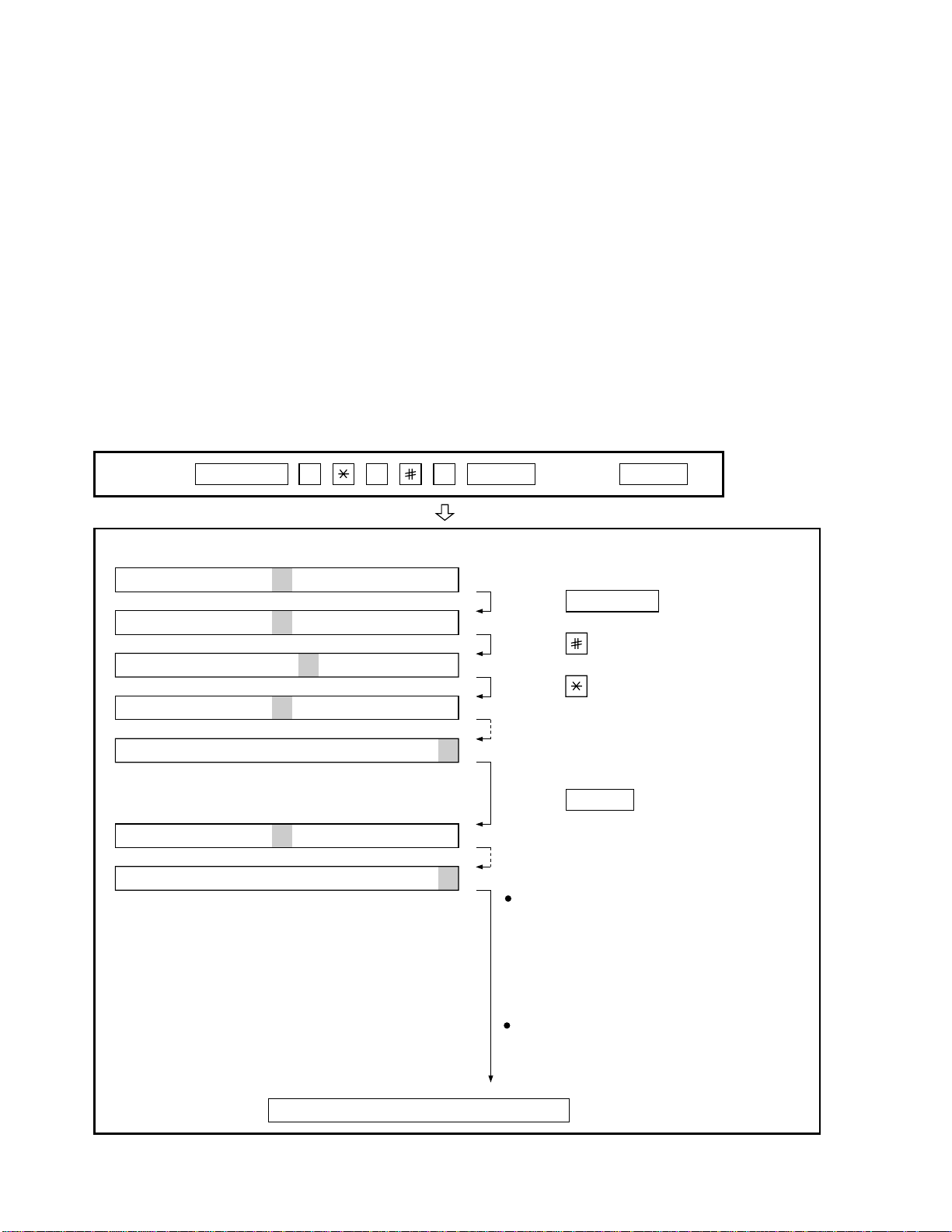
4. How to make soft switch setting
To enter the soft switch mode, press the following key entries in sequence.
Press
FUNCTION
9 8 7 START START
DATA No. 1 2 3 4 5 6 7 8
S F T SW-A1 = 0 0 0 0 0 0 0 0
S F T SW-A1 = 1 0 0 0 0 0 0 0
S F T SW-A1 = 1 0 0 0 0 0 0 0
S F T SW-A1 = 1 0 0 0 0 0 0 0
S F T SW-A1 = 1 0 0 0 0 0 0 0
S F T SW-A2 = 0 0 0 0 0 0 0 0
S F T SW-N3 = 0 0 0 0 0 0 0 0
Press FUNCTION key.
Press key.
Press key.
Bit1 - 8 are set.
Press key during setting.
START
Soft SW-A2 - SW-N3 are set.
To finish the settings halfway between
SW-A1 and SW-N3, press the STOP
key. In this case, the setting being done
to the SW No. on display will be nullified
while settings done to the preceding
SW Nos. remain in effect.
When the COPY key is pressed, the
contents of soft switches are printed.
The soft switch mode is terminated.
2 – 4
Page 17

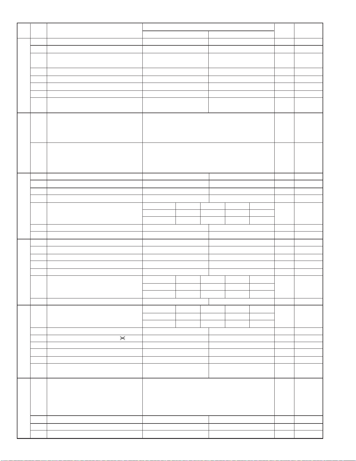
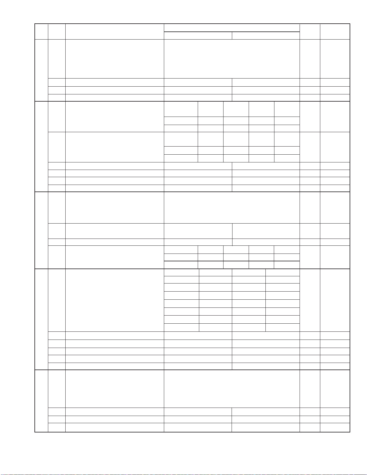
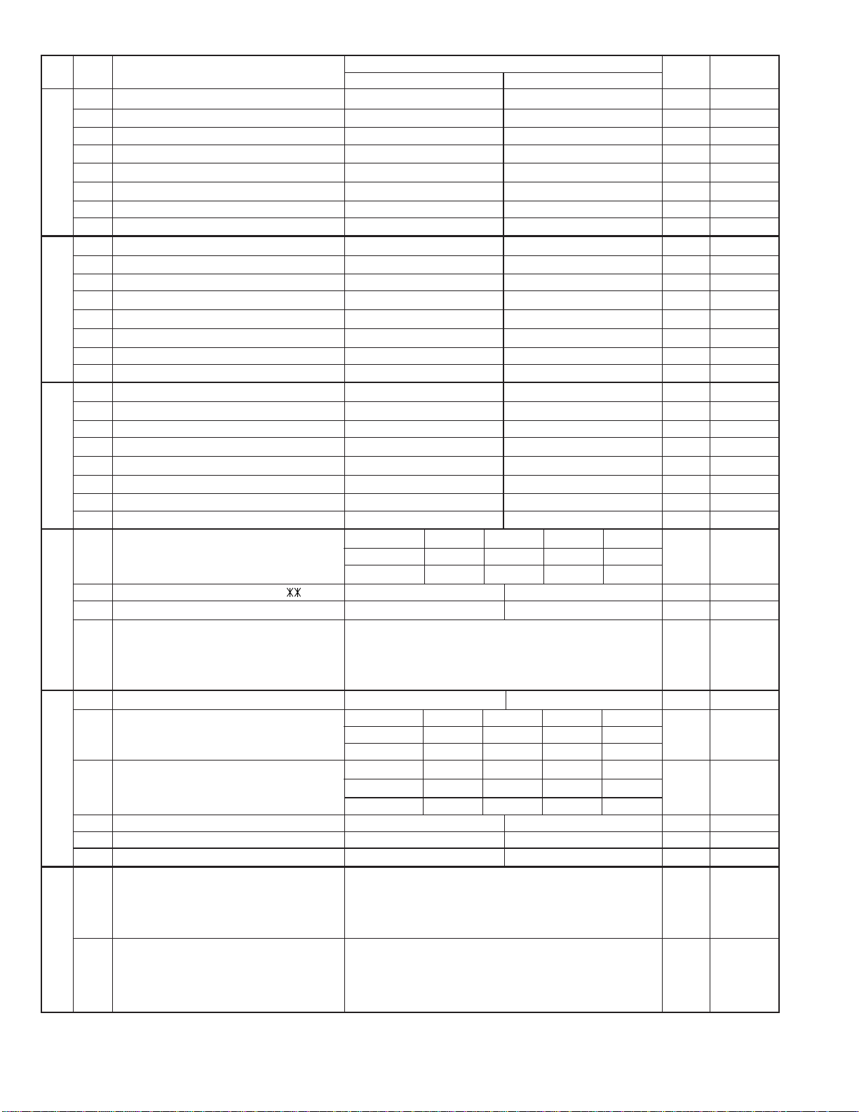
5. Soft switch description
• Soft switch
UX-510UA
FO-1470U
SW
NO.
SW
A1
SW
A2
SW
A3
SW
A4
SW
A5
DATA
NO.
1 Protect from echo No Yes 0
2 Forced 4800 BPS reception Yes No 0
3 Footer print Yes No 0
4 Length limitation of copy/send/receive No limit Copy/send: 1m 0
5 CSI transmission No transmitted Transmitted 0
l
6 DIS receive acknowledgement during G3 Twice NSF: Once 0
transmission DIS: Twice
7 Non-modulated carrier for V29 transmission Yes No 0
modem
8 EOL detect timer 25 s 13 s 0
Modem speed V.33 V.17 V.29 V.27 ter
1 0011110000 1
2 1100000000 0
3 0101010110 0
4 0000111100 0
l
5 Sender’s information transmit No Yes 0
6 Reserved 0
7 Communication error treatment in RTN No communication error Communication error 0
sending mode (reception)
8 CNG transmission No Yes 0
CED tone signal interval 1000ms 750ms 500ms 75ms
1 No. 1 1 1 0 0 0
2 No. 2 1 0 1 0 0
3 MR coding No Yes 0
l
4 ECM mode No Yes 0 OPTION
5 ECM MMR mode No Yes 0
6 Reserved 0
7 Reserved 0
8 Reserved 0
1 Signal transmission level Binary input 0
2 No. = 16 8 4 2 1 1
3 1 2 3 4 5 0
4 0 1 0 1 0 1
l
5 0
6 Protocol monitor (error print) Printed at com. error Not printed 0
7 Protocol monitor Yes No 0
8 Line monitor Yes No 0
Digital line equalization setting (Reception) 7.2km 3.6km 1.8km 0km
1 No. 111000
2 No. 210101
Digital line equalization setting 7.2km 3.6km 1.8km 0km
3 (Transmission) No. 3 1 1 0 0 0
l
4 No. 410101
Digital cable equalizer setting (Reception 7.2km 0km
5 for Caller ID) No. 5 1 0 1
6No. 6101
7 Error criterion 10 ~ 20 % 5 ~ 10 % 0
8 Anti junk fax check Yes No 0 OPTION
ITEM
14400 12000 14400 12000 9600 7200 9600 7200 4800 2400
Switch setting and function
10
Receive: 1.5m
Initial
setting
Remarks
2 – 5
Page 18
UX-510UA
FO-1470U
SW
DA TA
NO.
NO.
1 Auto gain control (MODEM) Enable Disable 1
2 End Buzzer Yes No 1
3 Disconnect the line when DIS is received in No Yes 1
SW
l
A6
SW
l
B1
SW
l
B2
SW
l
B3
SW
l
B4
SW
l
B5
RX mode
4 Equalizer freeze control (MODEM) On Off 0
5 Equalizer freeze control 7200BPS only No Yes 0
6 CNG transmission in manual TX mode Yes No 1
7 Reserved 0
8 Modem speed automatic fallback when RX Yes No 0
level is under -40dBm
1 Recall interval Binary input 0 OPTION
2 No. = 8 4 2 1 1
3 1 2 3 4 0
4 0 1 0 1 1
5 Recall times Binary input 0 OPTION
6 No. = 8 4 2 1 0
7 5 6 7 8 1
8 0 0 1 0 0
1 Dial pausing (sec/pause) 4 sec 2 sec 0
2 Dial tone detection (before outo dial) No Yes 1
3 Reserved 0
4 Busy tone detection (after auto dial) No Yes 0
Waiting time after dialing
5No.500110
6No.601010
7 Reserved 0
8 Reserved 0
1 Reserved 0
2 Reserved 0
3 Reserved 0
4 Reserved 0
5 Reserved 0
Auto dial mode Delay timer of before line
6 connect No.6 0 0 1 1 0
7No.701010
8 Hold key Enable Disable 1
Auto dial mode Delay timer of after line
1 connect No.1 0 0 1 1 0
2No.201010
3 Dial mode Tone Pulse 1 OPTION
4 Pulse → Tone change function by key Enable Disable 1
5 Dial pulse make/break ratio (%) 40/60 33/67 1
6 Reserved 0
7 Reserved 0
8
Recalling fixed only one time when dialing was
unsuccessful without detecting busy tone signal
1 DTMF signal transmission level (Low) Binary input 0
2 No. = 16 8 4 2 1 1
3 1 2 3 4 5 0
4 0 1 0 1 1 1
5 1
6 Reserved 0
7 Reserved 0
8 Reserved 0
ITEM
Yes No 1
Switch setting and function
1
45 seconds 55 seconds 90 seconds 140 seconds
0 second 1.5 seconds 3.0 seconds 4.5 seconds
1.7 seconds 3.0 seconds 3.6 seconds 4.0 seconds
0
Initial
setting
Remarks
2 – 6
Page 19
UX-510UA
FO-1470U
SW
NO.
SW
B6
SW
C1
SW
D1
SW
D2
SW
D3
DATA
NO.
1 DTMF signal transmission level (High) Binary input 0
2 No. = 16 8 4 2 1 0
3 1 2 3 4 5 1
4 0 0 1 1 1 1
l
5 1
6 Dial tone detection (LCR center call) No Yes 0
7 Reserved 0
8 Reserved 0
Reading slice (Binary) Factory Light Dark Darker in
1No. 101010
2 No. 2 0 0 1 1 0
Reading slice (Half tone) Factory Light Dark Darker in
l
3No. 301010
4No. 400110
5 Line density selection Fine Standard 0 OPTION
6 Reserved 0
7 MTF correction in half tone mode No Yes 0
8 Reserved 0
1 Number of rings for auto receive Binary input 0 OPTION
2 No. = 8 4 2 1 1
3 1 2 3 4 0
4 0 1 0 0 0
5 Automatic switching manual to auto receive Reception after 5 rings No reception 0
l
l
l
mode
6 Reserved 0
Cl detect frequency
7 No.700110
8 No.801010
Distinctive ringing setting No. 1 No. 2 No. 3 OPTION
(PATTERN 4 and 5 are for CANADA only) OFF 0 0 0
1 PATTERN3 1 0 0 0
2 PATTERN4 1 0 1 0
3 PATTERN5 1 1 0 0
4 Reserved 0
5 Caller ID function Yes No 0 OPTION
6 Caller ID detect during CI off All times Only first 0
7 Reserved 0
8 Reserved 0
1 Cl off detection timer (0-1550ms setting by Binary input 0
2 50ms step) No. = 16 8 4 2 1 1
3 1 2 3 4 5 1
4 0 1 1 1 0 1
5 0
6 Reserved 0
7 Reserved 0
8 Reserved 0
ITEM
STANDARD 0 0 1
PATTERN1 0 1 0
PATTERN2 0 1 1
Switch setting and function
1
setting dark
setting dark
As PTT 11.5Hz 13.0Hz 20.0Hz
0
Initial
setting
Remarks
2 – 7
Page 20
UX-510UA
FO-1470U
SW
DA TA
NO.
NO.
1 Reserved 0
2 Reserved 0
3 Reserved 0
SW
4 Reserved 0
l
5 Reserved 0
E1
6 Reserved 0
7 Reserved 0
8 Reserved 0
1 Reserved 0
2 Reserved 0
3 Reserved 0
SW
4 Reserved 0
l
5 Reserved 0
E2
6 Reserved 0
7 Reserved 0
8 Reserved 0
1 Reserved 0
2 Reserved 0
3 Reserved 0
SW
4 Reserved 0
l
5 Reserved 0
E3
6 Reserved 0
7 Reserved 0
8 Reserved 0
DTMF detection time 50ms 80ms 100ms 120ms
1No. 100110
2No. 201010
3 Protection of remote reception (5 ) detect Yes No 0 OPTION
SW
l
4 Remote reception with GE telephone Compatible Not compatible 1
F1
5 Remote operation code figure by external Binary input 0 OPTION
6 TEL (0~9) No. = 8 4 2 1 1
7 5 6 7 8 0
8 0 1 0 1 1
1 CNG detection in STAND-BY mode Yes No 1 OPTION
Number of CNG detect (AM mode) 1pulse 2pulses 3pulses 4pulses
2No. 200110
3 No. 3 0 1 0 1 1
SW
l
F2
SW
l
G1
Number of CNG detect (STAND-BY mode) 1pulse 2pulses 3pulses 4pulses
4No. 400110
5 No. 5 0 1 0 1 1
6 Reserved 0
7 Reserved 0
8 Reserved 0
1 Quiet detect time Binary input 0 OPTION
2 No. = 8 4 2 1 1
3 1 2 3 4 0
4 0 1 0 0 0
5 Quiet detect start timing Binary input 0
6 No. = 8 4 2 1 1
7 5 6 7 8 0
8 0 1 0 1 1
ITEM
Switch setting and function
1
0
Initial
setting
Remarks
2 – 8
Page 21
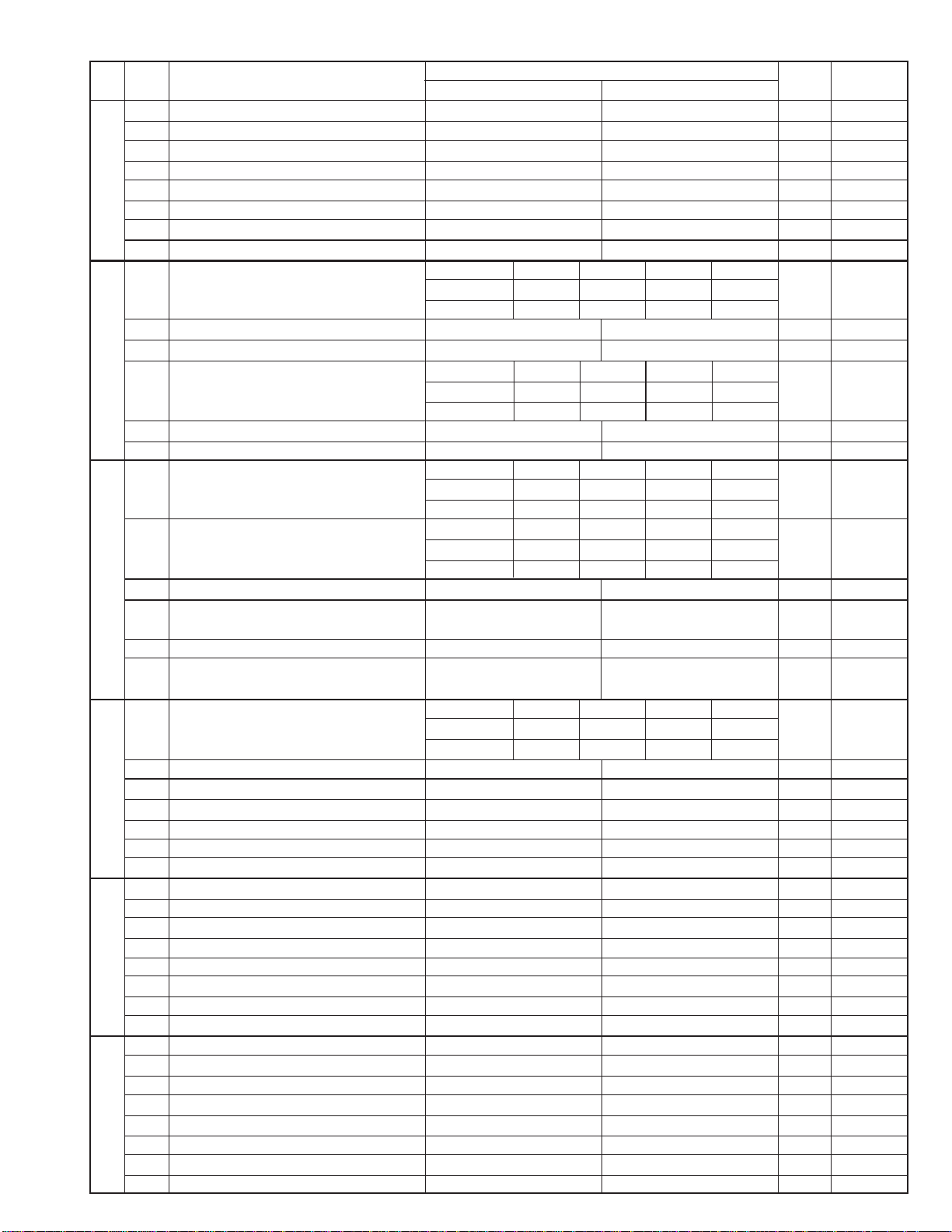
UX-510UA
FO-1470U
SW
NO.
SW
G2
SW
G3
SW
H1
SW
l
H2
SW
I1
SW
I2
DATA
NO.
1 Reserved 0
2 Reserved 0
3 Reserved 0
4 Reserved 0
l
5 Reserved 0
6 Reserved 0
7 Reserved 0
8 Reserved 0
OGM detect timer Not work 100ms 200ms 300ms
1No. 100110
2No. 201011
3 Reserved 0
4 Reserved 0
l
l
l
l
Selection time of quiet detection 30s 40s 50s 60s
5No. 500110
6No. 601011
7 Choice after quiet detect Wait response for 3sec Normal FAX RX 1
8 Reserved 0
Busy tone detection ON/OFF time (Lower 150ms 200ms 250ms 350ms
1 duration) No. 1 0 0 1 1 0
2No. 201011
Busy tone detection ON/OFF time (Upper 650ms 900ms 1500ms 2700ms
3 duration) No. 3 0 0 1 1 0
4No. 401011
5 Reserved 0
6 Busy tone detect continuation sound detect No Yes 0
(during ICM: for internal A.M.)
7 Reserved 0
8 Busy tone detect intermittent sound detect No Yes 0
(during ICM: for internal A.M.)
Busy tone detection pulse number 2pulses 4pulses 6pulses 10pulses
1No. 100110
2No. 201011
3 Fax switching when A.M. full Yes No 0 OPTION
4 Reserved 0
5 Reserved 0
6 Reserved 0
7 Reserved 0
8 Busy tone continuous sound detect time 5s 10s 1
1 Reserved 0
2 Reserved 0
3 Reserved 0
4 Reserved 0
5 Reserved 0
6 Reserved 0
7 Reserved 0
8 Reserved 0
1 Reserved 0
2 Reserved 0
3 Reserved 0
4 Reserved 0
5 Reserved 0
6 Reserved 0
7 Reserved 0
8 Reserved 0
ITEM
Switch setting and function
1
0
Initial
setting
Remarks
2 – 9
Page 22
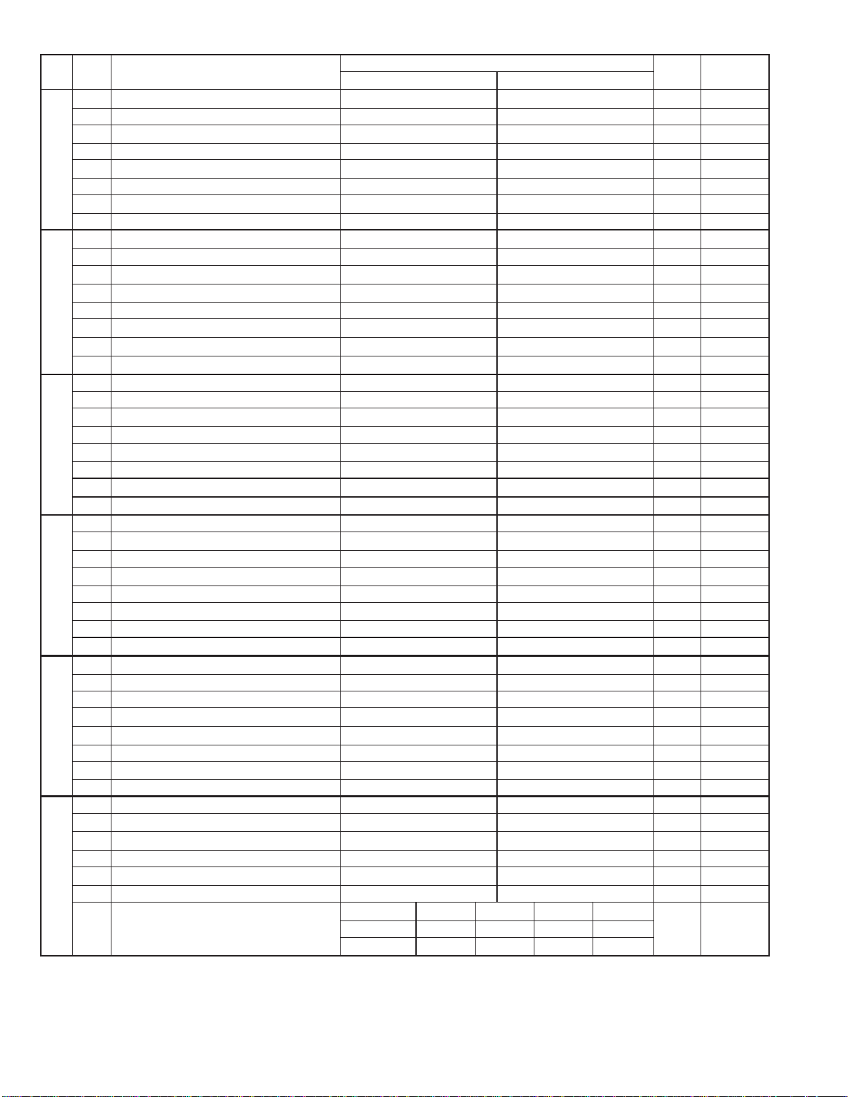
UX-510UA
FO-1470U
SW
DA TA
NO.
NO.
1 Reserved 0
2 Reserved 0
3 Reserved 0
SW
4 Reserved 0
l
5 Reserved 0
I3
6 Reserved 0
7 Reserved 0
8 Reserved 0
1 Reserved 0
2 Reserved 0
3 Reserved 0
SW
4 Reserved 0
l
5 Reserved 0
I4
6 Reserved 0
7 Reserved 0
8 Reserved 0
1 Reserved 0
2 Reserved 0
3 Reserved 0
SW
4 Reserved 0
l
5 Reserved 0
I5
6 Reserved 0
7 Reserved 0
8 Reserved 0
1 Reserved 0
2 Reserved 0
3 Reserved 0
SW
4 Reserved 0
l
5 Reserved 0
I6
6 Reserved 0
7 Reserved 0
8 Reserved 0
1 Reserved 0
2 Reserved 0
3 Reserved 0
SW
4 Reserved 0
l
5 Reserved 0
I7
6 Reserved 0
7 Reserved 0
8 Reserved 0
1 Activity report print Automatic printout No printout when memory full 0 OPTION
2 Total communication hours and pages print No Yes 0
3 Sender’s phone number setting Cannot change Change allowed 0
4 Reserved 0
SW
l
5 Reserved 0
J1
6 Summer time setting No Yes 1 OPTION
Ringer volume Off Low Middle High OPTION
7No. 700111
8No. 801010
ITEM
Switch setting and function
1
0
Initial
setting
Remarks
2 – 10
Page 23
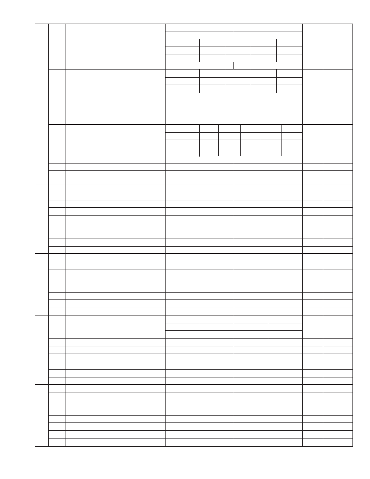
UX-510UA
FO-1470U
SW
NO.
SW
l
J2
SW
l
J3
SW
K1
SW
l
L1
SW
L2
SW
M1
DATA
NO.
Speaker volume (3 stages) Low Low Middle High OPTION
1No. 100111
2No. 201010
3 Polling key Yes No 0 OPTION
Handset receiver volume Low Low Middle High OPTION
4No. 400111
5No. 501010
6 Reserved 0
7 Reserved 0
8 Reserved 0
1 Automatic cover sheet Yes No 0 OPTION
Communication results printout E/T/M
(Transaction report)
2
3 No. 3001100
4 No. 4010100
5 Reserved 0
6 Reserved 0
7 Reserved 0
8 Reserved 0
1 Entering DIAG mode by pressing SPEED Yes No 0
key
2 Reserved 0
3 Reserved 0
4 Reserved 0
l
5 Reserved 0
6 Reserved 0
7 Reserved 0
8 Reserved 0
1 Reserved 0
2 Reserved 0
3 Reserved 0
4 Reserved 0
5 Cut off mode (COPY mode) Yes No 1 OPTION
6 A4 paper enable Enable Disable 0
7 LEGAL & LETTER paper enable Enable Disable 1
8 2 IN 1 Mode Yes No 0 OPTION
Paper set size LETTER LEGAL A4 OPTION
1No. 10010
2No. 20100
3 Automatic reduce of receive Auto 100 % 1 OPTION
4 Print contrast Light Normal 0 OPTION
l
5
Reception reduction ratio in case of memory full
6 Reserved 0
7 Reserved 0
8 Reserved 0
1 Reserved 0
2 Reserved 0
3 Reserved 0
4 Reserved 0
l
5 Reserved 0
6 Reserved 0
7 Reserved 0
8 Reserved 0
ITEM
No. 2000011
100 % 93 % 0 OPTION
Switch setting and function
1
Send only
Always No print Err only OPTION
0
Initial
setting
Remarks
2 – 11
Page 24
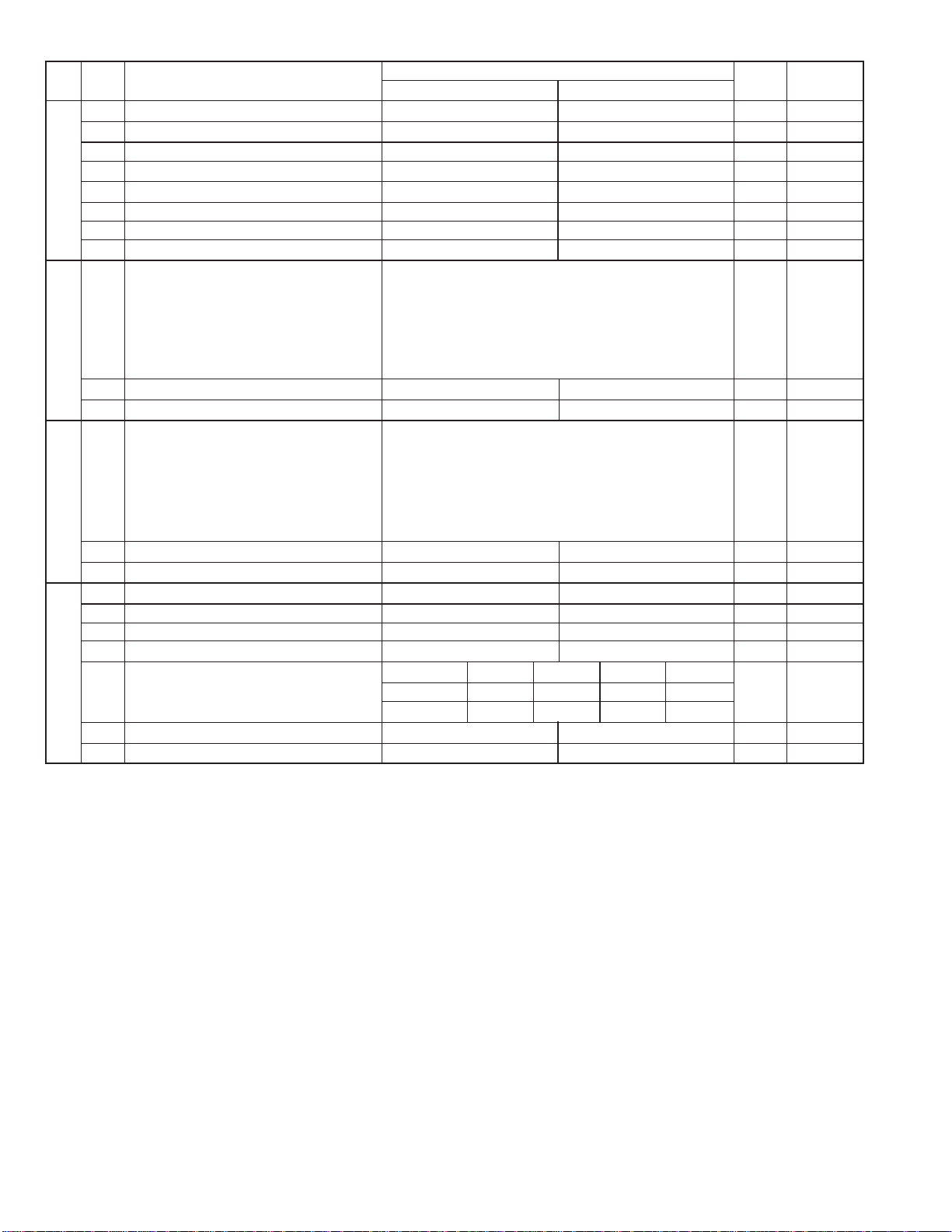
UX-510UA
FO-1470U
SW
DA TA
NO.
NO.
1 Reserved 0
2 Reserved 0
3 Reserved 0
SW
4 Reserved 0
l
5 Reserved 0
M2
6 Reserved 0
7 Reserved 0
8 Reserved 0
1 LCR short time Binary input 0 OPTION
2 No. =3216842 1 0
3 1 2 3 4 5 6 0
SW
4 0 0 0 0 1 0 0
l
5 1
N1
6 0
7 Reserved 0
8 Reserved 0
1 LCR long time Binary input 0 OPTION
2 No. =3216842 1 0
3 1 2 3 4 5 6 0
SW
4 0 0 0 1 0 0 1
l
5 0
N2
6 0
7 Reserved 0
8 Reserved 0
1 LCR Time Select Long Short 0 OPTION
2 Temporary release of caller ID withhold Yes No 1
3 Connect Japanese center Connect Japanese center Connect USA center 0
4 Open LCR debug mode Open LCR debug mode ON Open LCR debug mode OFF 0
SW
l
N3
Digital equalization setting (Reception for 0km 0km 7.2km 7.2km
5 LCR V23 mode) No. 5 0 0 1 1 0
6No. 601010
7 Reserved 0
8 Reserved 0
ITEM
Switch setting and function
1
0
Initial
setting
Remarks
2 – 12
Page 25
• Soft switch function description
SW-A1 No. 1 Protect from echo
Used to protect from echo in reception.
SW-A1 No. 2 Forced 4800BPS reception
When line conditions warrant that receptions take place at 4800BPS
repeatedly.
It may improve the success of receptions by setting at 4800BPS.
This improves the receiving document quality and reduces handshake
time due to fallback during training.
SW-A1 No. 3 Footer print
When set to "1", the date of reception, the sender machine No., and the
page No. are automatically recorded at the end of reception.
SW-A1 No. 4 Length limitation of copy/send/receive
Used to set the maximum page length.
To avoid possible paper jam, the page length is normally limited to 1
meter for copy or transmit, and 1.5 meters for receive.
It is possible to set it to "No limit" to transmit a long document, such as a
computer print form, etc. (In this case, the receiver must also be set to
no limit.)
SW-A1 No. 5 CSI transmission
(CSI TRANSMISSION) is a s witch to set whether the machine sends or
does not send the signal (CSI signal) informing its own telephone No. to
the remote fax machine when information is received. When "nonsending"
is set, the telephone No. is not output on the remote transmitting machine if the remote transmitting machine has the function to display or
print the telephone No. of receiving machine, using this CSI signal.
SW-A1 No. 6 DIS receive ackno wledgment during G3 transmission
Used to make a choice of whether reception of DIS (NSF) is acknowledged after receiving two DISs (NSFs) or receiving one DIS (two NSFs).
It may be useful for overseas communication to avoid an echo suppression problem, if set to 1.
SW-A1 No. 7 Non-modulated carrier for V29 transmission modem
Though transmission of a non-modulated carrier is not required for transmission by the V29 modem according to the CCITT recommendation, it
may be permitted to a send non-modulated carrier before the image
signal to avoid an echo suppression problem. It may be useful for overseas communication to avoid an echo suppression problem, if set to 1.
SW-A1 No. 8 EOL (End Of Line) detect timer
Used to make a choice of whether to use the 25-second or 13-second
timer for detection of EOL.
This is effective to override communication failures with some facsimile
models that have longer EOL detection.
SW-A2 No. 1 ~ No. 4 Modem speed
Used to set the initial modem speed. The default is 9600BPS.
It may be necessary to program it to a slower speed when frequent line
fallback is encountered, in order to save the time required for fallback
procedure.
SW-A2 No. 5 Sender’s information transmit
(SENDER’S INFORMATION TRANSMISSION) is a switch to set the
function to print the content of HEADER PRINT described in the passcode
list at the front end of receiver’s or iginal when original is sent to the
remote machine.
If this switch is set to "NO", the HEADER PRINT is not output at the
receiving machine.
SW-A2 No. 6 Reserved
Set to "0".
SW-A2 No. 7 Communication error treatment in R TN sending mode
(Reception)
Used to determine communication error treatment when RTN is sent by
occurrence of a received image error in G3 reception. When it is set to
"1", communication error is judged as no error.
UX-510UA
FO-1470U
SW-A2 No. 8 CNG transmission
When set to "0" , this model allows CNG transmission by pressing the
Start key in the key pad dialing mode. When set to "1", CNG transmission in the key pad dialing mode cannot be perfor med. In either case.
CNG transmission can be performed in the auto dial mode.
SW-A3 No. 1, No. 2 CED tone signal interval
For international communication, the 2100Hz CED tone may act as an
echo suppression switch, causing a communication problem.
Though SW-A3 No . 1 and No . 2 are normally set to 0, this selfing is used
to change the time between the CED tone signal to eliminate the communication caused by echo.
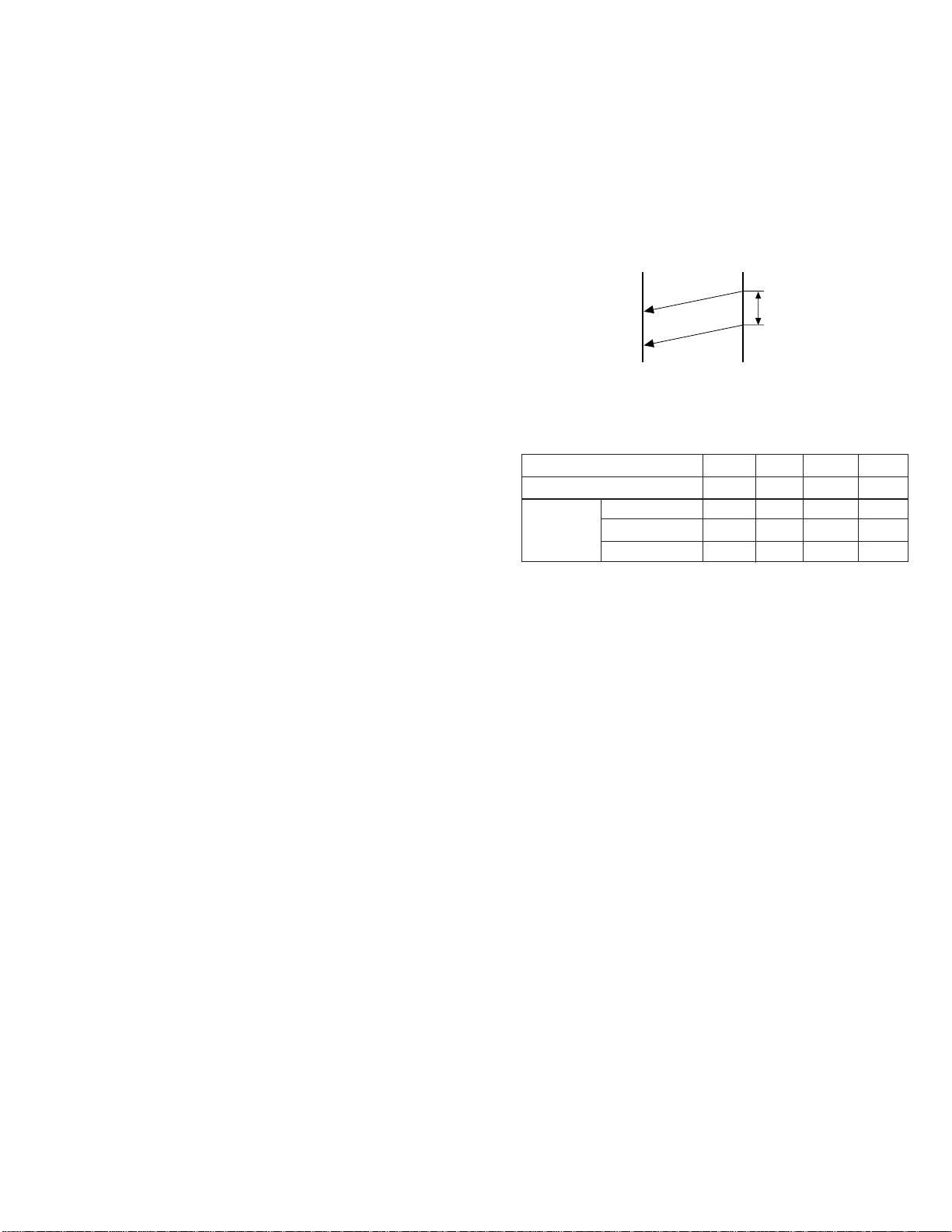
TX RX
CED
T
DIS
SW-A3 No. 3 MR Coding
MR Coding is enable.
SW-A3 No. 4 ECM mode
Used to determine ECM mode function. Refer to following table.
SW-A3 No.4 ECM MODE 0 0 1 1
SW-A3 No.5 ECM MMR MODE 0 1 0 1
Compression
method
(Depending on remote machine)
SW-A3 No. 5 ECM MMR mode
See SW-A3 No. 4.
SW-A3 No. 6 ~ No. 8 Reserved
Set to "0".
SW-A4 No. 1 ~ No. 5 Signal transmission level
Used to control the signal transmission level in the range of-0dB to31dB.
SW-A4 No. 6 Protocol monitor (Error print)
If set to "1", protocol is printed at communication error.
SW-A4 No. 7 Protocol monitor
Normally set to "0". If set to "1", communication can be chec ked, in case
of trouble, without using a G3 tester or other tools.
When communication FSK data transmission or reception is made, the
data is taken into the buffer . When communication is finished, the data is
analysed and printed out. When data is received with the line monitor
(SW-A4 No. 8) set to "1" the reception level is also printed out.
SW-A4 No. 8 Line monitor
Normally set to "0". If set to "1", the transmission speed and the reception level are displayed on the LCD. Used for line tests.
SW-A5 No. 1, No. 2 Digital line equalization setting (Reception)
Line equalization when reception is to be set according to the line characteristics.
Setting should be made according to distance between the telephone
and the telephone company central switching station.
SW-A5 No. 3, No. 4 Digital line equalization setting (Transmission)
Line equalization when transmitter is to be set according to the line
characteristics.
Setting should be made according to distance between the telephone
and the telephone company central switching station.
ECM MMR mode Yes No No No
ECM MH mode Yes Yes No No
MR Mode Yes Yes Yes Yes
2 – 13
Page 26
UX-510UA
FO-1470U
SW-A5 No. 5, No. 6 Digital cable equalizer setting
(Reception for Caller ID)
Line equalization when reception for CALLER ID is to be set according
to the line characteristics.
Setting should be made according to distance between the telephone
and the telephone company central switching station.
SW-A5 No. 7 Error criterion
Used to select error criterion for sending back RTN when receiving image data.
SW-A5 No. 8 Anti junk fax check
When using the Anti junk fax function, set to "1".
SW-A6 No. 1 Auto gain control (MODEM)
When this mode is enabled, if the reception signal lev el is under 31dBm,
the modem itself controls the signal gain automatically.
SW-A6 No. 2 End buzzer
Setting this bit to 0 will disable the end buzzer (including the error b uzzer/
on-hook buzzer).
SW-A6 No. 3 Disconnect the line when DIS is received in RX mode
Bit1= 0: When DIS signal is received during RX mode, the line is disconnected immediately.
Bit1= 1: When DIS signal is received during RX mode, the line is disconnected on the next tone.
SW-A6 No. 4 Equalizer freeze control (MODEM)
This switch is used to perform reception operation by fixing the equalizer control of modem for the line which is alwa ys in an unfa vorable state
and picture cannot be received.
* Usually, the control is executed according to the state of line where
the equalizer setting is changed always.
SW-A6 No. 5 Equalizer freeze control 7200BPS only
Setting which specifies SW-A3 No. 6 control only in the condition of
7200BPS modem speed.
SW-A6 No. 6 CNG transmission in manual TX mode
When set to "1", fax transmit the CNG signal in case of manual transmission mode (User press the START key after waiting for the fax answering signal from handset or speaker).
SW-A6 No. 7 Reserved
Set to "0".
SW-A6 No. 8 Modem speed automatic fallback when RX level is
under -40dBm
When set to "1", if fax signal level is under -40dBm during reception,
machine selects the slower modem speed automatically.
It is effective when noises occur on the received document due to the
long distance communications.
SW-B1 No. 1 ~ No. 4 Recall interval
Choice is made for a redial interval for speed and rapid dial calls.
Use a binary number to program this. If set to 0 accidentally, 1 will be
assumed.
SW-B1 No. 5 ~ No. 8 Recall times
Choice is made as to how many redials there should be.
SW-B2 No. 1 Dialing pause (sec/pause)
Pauses can be inserted between telephone numbers of direct dial connection. Selection of 4 sec or 2 sec pause is available.
SW-B2 No. 2 Dial tone detection (before auto dial)
Used to set YES/NO of dial tone detection in auto dialing.
SW-B2 No. 3 Reserved
Set to "0".
SW-B2 No. 4 Busy tone detection (after auto dial)
Used to set busy tone detection in auto dialing.
SW-B2 No. 5, No. 6 Waiting time after dialing
This is time waiting for the opponent’s signals after dialing.
SW-B2 No. 7, No. 8 Reserved
Set to "0".
SW-B3 No. 1 ~ No. 5 Reserved
Set to "0".
SW-B3 No. 6, No. 7 Auto dial mode Delay timer of before line connect
Delay time between the dial key input and line connection under the
auto dial mode.
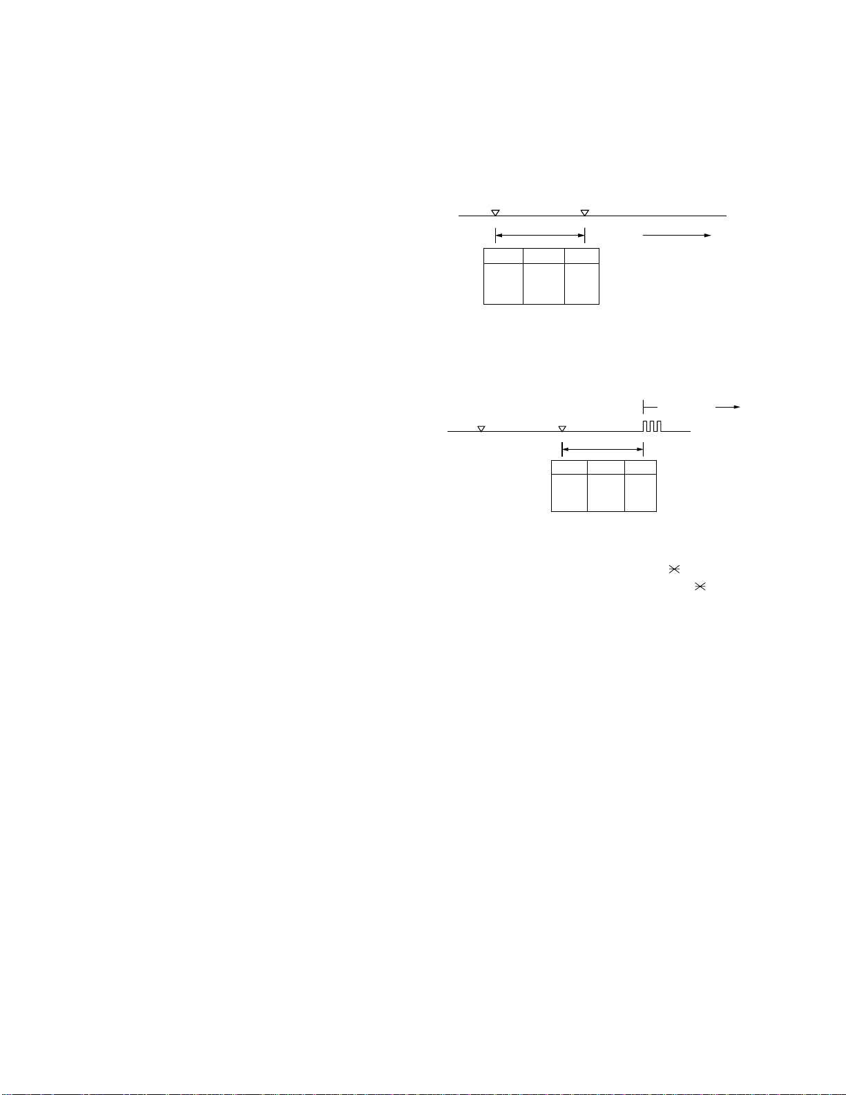
RAPID01 CML RELAY ON
DIALLING
No.6 No.7
0 0 0sec
0 1 1.5sec
1 0 3.0sec
1 1 4.5sec
SW-B3 No. 8 Hold key
Used to set YES/NO of holding function by the HOLD key.
SW-B4 No. 1, No. 2 A uto dial mode Delay timer of after line connect
Delay time between the line connection and dial data output under the
auto dial mode.
RAPID01 CML RELAY ON
No.1 No.2
0 0 1.7sec
0 1 3.0sec
1 0 3.6sec
1 1 4.0sec
DIAL DATA
SW-B4 No. 3 Dial mode
When using the pulse dial, set to 1. When using the tone dial, set to 0.
SW-B4 No. 4 Pulse → Tone change function by key
When setting to 1, the mode is changed by pressing the key from the
pulse dial mode to the tone dial mode.
SW-B4 No. 5 Dial pulse make/break ratio (%)
When using the 33% make ratio pulse dial, set to "0".
When using the 40% make ratio pulse dial, set to "1".
SW-B4 No. 6, No. 7 Reserved
Set to "0".
SW-B4 No. 8 Recalling fixed only one time when dialing was unsuccessful without detecting busy tone signal
When dialing results in failure since the busy tone cannot be detected,
recalling is fixed to one time.
Supplementary explanation
If time-out termination is made when dialing, only single recall is possible even if the setting time of recalls (SW-B1 No. 5 - No. 8) has been set
to some times. This soft switch is added in order to meet FCC.
SW-B5 No. 1 ~ No. 5 DTMF signal transmission level (Low)
The transmission level of DTMF signal is adjusted. (lower frequency)
00000: 0dBm
↓
11111: -15.5dBm (-0.5dBm x 31)
SW-B5 No. 6 ~ No. 8 Reserved
Set to "0".
SW-B6 No. 1 ~ No. 5 DTMF signal transmission level (High)
The transmission level of DTMF signal is adjusted. (higher frequency)
00000: 0dBm
↓
11111: -15.5 dBm (-0.5dBm x 31)
2 – 14
Page 27
SW-B6 No. 6 Dial tone detection (LCR center call)
Used to set YES/NO of dial tone detection (calling LCR center).
SW-B6 No. 7, No. 8 Reserved
Set to "0".
SW-C1 No. 1, No. 2 Reading slice (Binary)
Used to determine the set value of reading density in standard/fine mode.
The standard setting is "00" (Factory setting is "00")
SW-C1 No. 3, No. 4 Reading slice (Half tone)
Used to determine the set value of reading density in half tone mode.
The standard setting is "00" (Factory setting is "00")
SW-C1 No. 5 Line density selection
Used to set the transmission mode which is automatically selected when
the Resolution key is not pressed. In the copy mode, however, the fine
mode is automatically selected unless the Resolution key is manually
set to another mode.
SW-C1 No. 6 Reserved
Set to "0".
SW-C1 No. 7 MTF correction in half tone mode
This allows selection of MTF correction (dimness correction) in the half
tone mode.
When "NO" (=1) is selected, the whole image becomes soft and mild.
Clearness of characters will be reduced. Normally set to "YES" (=0).
SW-C1 No. 8 Reserved
Set to "0".
SW-D1 No. 1 ~ No. 4 Number of rings for auto receive
When the machine is set in the auto receive mode, the number of rings
before answering can be selected. It may be set from one to four rings
using a binary number. Since the facsimile telephone could be used as
an ordinary telephone if the handset is taken off the hook, it should be
programmed to the user’s choice. If the soft switch was set to 1, direct
connection is made to the facsimile. If a facsimile calling beep w as heard
when the handset is taken off the hook, press the START key and put
the handset on the hook to have the facsimile start receiving. If it was set
to 0 accidentally, receive ring is set to 1.
NOTE: If the machine is set to answer after a large number of rings, it
may not be able to receive faxes successfully. If you have difficulty receiving faxes, reduce the number of rings to a maximum
of 6.
SW-D1 No. 5 Automatic switching manual to auto receive mode
This soft switch is used to select whether the machine should switch to
the auto receive mode after 5 rings in the manual receive mode or remain in the same way as SW -D1 No. 1, No . 2, No . 3 and No. 4 "0"1"0"1"(5
rings).
SW-D1 No. 6 Reserved
Set to "0".
SW-D1 No. 7, No. 8 CI detect frequency
Detection frequency of ring signal for auto reception is set.
When set to No. 6=0, No . 7=0, frequency is set to PTT recommendation.
When set to No. 6=0, No. 7=1, frequency is set to 11.5Hz or more.
When set to No. 6=1, No. 7=0, frequency is set to 13.0Hz or more.
When set to No. 6=1, No. 7=1, frequency is set to 20.0Hz or more.
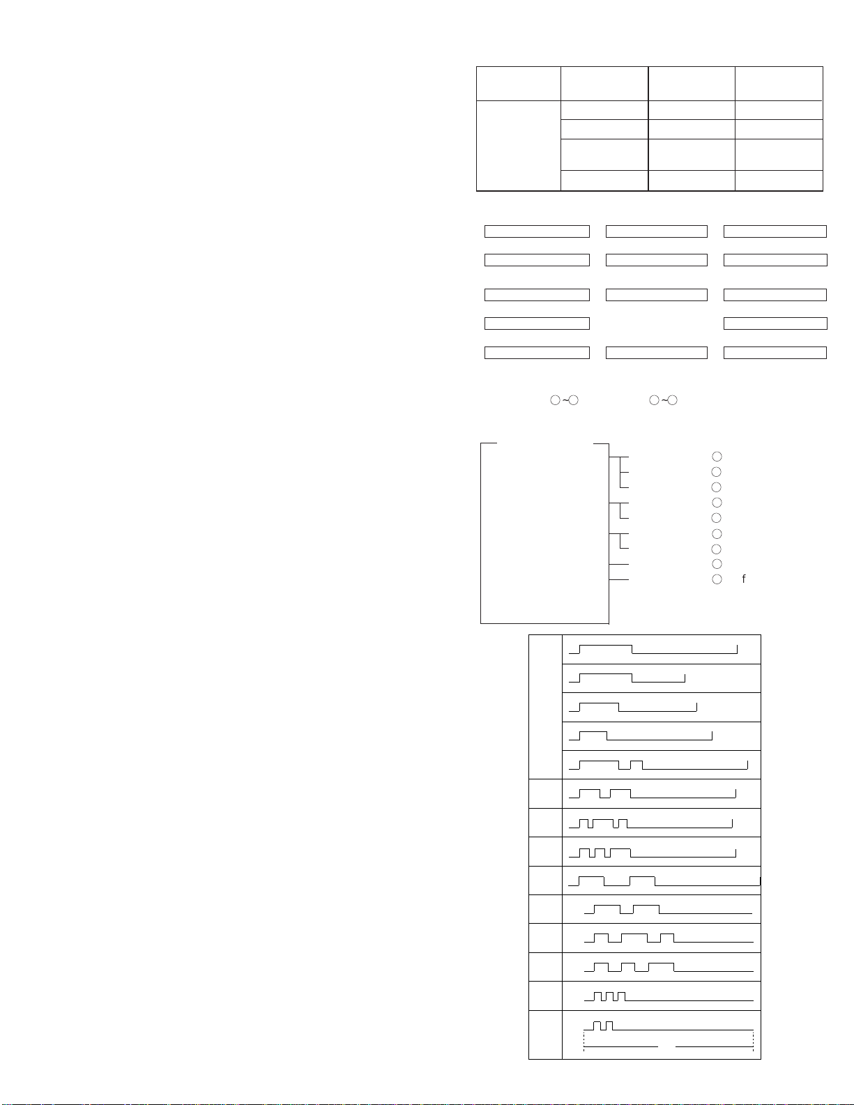
SW-D2 No. 1 ~ No. 3 Distinctive ringing setting (PATTERN 4 and 5
are for CANADA only)
This function allows reception of services offered by USA and Canada
telephone companies in which the customer contracts with the telephone
company to have up to 4 telephone numbers (USA) or 6 telephone numbers (Canada) established for one line.
Each telephone number is signalled by a different ringing pattern, and
the customer can allocate each number to a specific use.
UX-510UA
FO-1470U
<Example of use>
Phone Number Intended Ring Pattern
Purpose
Ring Pattern 555-1234 Voice Calls Standard
555-1235 Facsimile Calls Pattern 1
555-1236 Answering Pattern 2
Machine
555-1237 PC Modem Pattern 3
<Distinctive Ringing Timing Specifications>
1) USA
DISTINCTIVE RING → 1:RING PATTERN 1 → 2:RING PATTERN 2
↑↓
5:OFF SETTING ←
4:STANDARD RING
← 3:RING PATTERN 3
2) Canada
DISTINCTIVE RING → 1:RING PATTERN 1 → 2:RING PATTERN 2
↑↓
7:OFF SETTING 3:RING PATTERN 3
↑↓
6:
STANDARD RING←5:
RING PATTERN 5 ← 4:RING PATTERN 4
• Ring Pattern
STANDARD has 5 ring patterns, and DISTINCTIVE has 9 patterns.
Ring patterns 1~4 for USA, and 5~9 for Canada.
However, to make the setting procedure as easy as possible for the
user to understand these patterns are grouped as follows:
<Optional Setting>
1) RING PATTERN 1 RING PATTERN 1 for USA
RING PATTERN 4 for USA
RING PATTERN 5 for Canada
2) RING PATTERN 2 RING PATTERN 2 for USA
RING PATTERN 6 for Canada
3) RING PATTERN 3 RING PATTERN 3 for USA
RING PATTERN 7 for Canada
4) RING PATTERN 4 RING PATTERN 8 for Canada
5) RING PATTERN 5 RING PATTERN 9 for Canada
6) STANDARD RING
7) OFF SETTING
2S ring
STANDARD
RING
PATTERN 1
for USA
RING
PATTERN 2
for USA
RING
PATTERN 3
for USA
RING
PATTERN 4
for USA
RING
PATTERN 5
for CANADA
RING
PATTERN 6
for CANADA
RING
PATTERN 7
for CANADA
RING
PATTERN 8
for CANADA
RING
PATTERN 9
for CANADA
1.5S ring
1S ring
1.5S ring
0.8S
0.3S
0.2S
0.4S
0.2S 0.2S
0.25S
0.25S
2S ring
0.4S
1S
0.4S 0.8S
1S
1S 1S
0.5S
0.5S
0.25S
0.2S
0.2S
0.25S
0.2S
0.5S
0.8S
0.2S
1S
0.3S
0.5S
1S
0.5S
1S 0.5S
0.5S
0.5S0.5S
0.25S
2S ring
3S ring
4S ring
4S ring
4S ring
4S ring
4S ring
4S ring
4S ring
0.5S0.5S
1S
6S
2 – 15
Page 28
UX-510UA
2
FO-1470U
SW-D2 No. 4 Reserved
Set to "0".
SW-D2 No. 5 Caller ID function
Used for Caller ID function.
SW-D2 No. 6 Caller ID detect during CI off
Detection of caller ID signal is performed as follows:
0:First CI OFF only
1:All of CI OFF
SW-D2 No. 7, No. 8 Reserved
Set to "0".
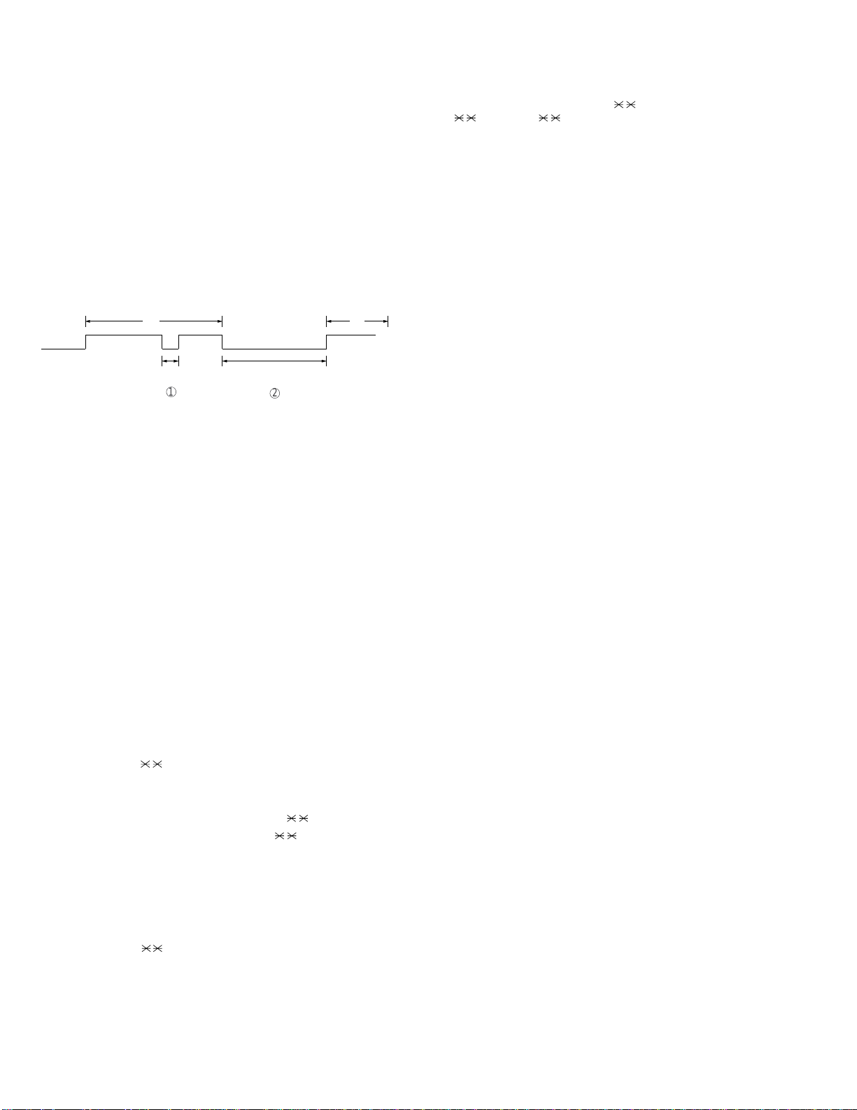
SW-D3 No. 1 ~ No. 5 CI off detection timer (0-1550ms setting by
50ms step)
Set the minimum time period of CI signal interruption which affords to be
judged as a CI OFF section with 50ms steps.
(Example)
AB
400msec
2000msec
1
01110 (50ms ~ 14):
700ms (CI interruption>700ms:Judged as a CI OFF section)
The section 1 is not judged as a CI OFF section, the CI signal A
is counted as one signal.
The section 2 is judged as a CI OFF section, the CI signal B is
considered as the second signal.
00111 (50ms ~ 7):
350ms (CI interruption>350ms:Judged as a CI OFF section)
The section 1 is judged as a CI OFF section, and the CI signal A
is counted as two signals.
The section 2 is judged as a CI OFF section, and the CI signal B
is considered as the third signal.
SW-D3 No. 6 ~ No. 8 Reserved
Set to "0".
SW-E1 No. 1 ~ No. 8 Reserved
Set to "0".
SW-E2 No. 1 ~ No. 8 Reserved
Set to "0".
SW-E3 No. 1 ~ No. 8 Reserved
Set to "0".
SW-F1 No. 1, No. 2 DTMF detect time
Used to set detect time of DTMF (Dual Tone Multi Frequency) used in
remote reception (5 ).
The longer the detect time is, the less the error detection is caused by
noises.
SW-F1 No. 3 Protection of remote reception (5 ) detect
Used to set the function of remote reception (5 ). When set to "1",
the remote reception function is disabled.
SW-F1 No. 4 Remote reception with GE telephone
(Corresponding to TEL made by GE) P. B. X.
"1": Compatible with TEL mode by GE
"0": Not compatible
• When sending (5 ) f or remote reception with a GE manuf actured
telephone remote reception may not take place because of special
specifications in their DTMF.
To overcome this, a soft SW is provided to change the modem set-
ting to allow for remote reception.
• If this soft SW is set to "1", other telephone sets may be adversely
affected.
SW-F1 No. 5 ~ No. 8 Remote operation code figure by external TEL
(0 ~ 9)
Remote operation codes can be changed from 0 through 9. If set to
greater than 9, it defaults to 9. The "5 " is not changed.
Ex-7 (Default: 5 )
SW-F2 No. 1 CNG detection in STAND-BY mode
When setting to "1", the CNG signal detection function during standby
stops.
SW-F2 No. 2, No. 3 Number of CNG detect (AM mode)
Used for detection of CNG in 1 to 4 pulses.
SW-F2 No. 4, No. 5 Number of CNG detect (STAND-BY mode)
Used for detection of CNG in 1 to 4 pulses.
SW-F2 No. 6 ~ No. 8 Reserved
Set to "0".
SW-G1 No. 1 ~ No. 4 Quiet detect time
When an answering machine is connected, if a no sound state is detected for a certain period of time, the machine judges it as a transmission from a facsimile machine and automatically switches to the FAX
mode.
SW-G1 No. 5 ~ No. 8 Quiet detect start timing
Inserts a pause before commencing quiet detection.
SW-G2 No. 1 ~ No. 8 Reserved
Set to "0".
SW-G3 No. 1, No. 2 OGM detect timer
This is used to change the OGM detection time for answering machine
hook up detection.
SW-G3 No. 3, No. 4 Reserved
Set to "0".
SW-G3 No. 5, No. 6 Selection time of quiet detection
The switch which sets the time from the start of detection function to the
end of the function.
SW-G3 No. 7 Choice after quiet detect
"0": The reception begins when no sound is detected in A.M. mode.
"1": The DIS signal is transmitted only once when no sound is detected
in A.M. mode.
SW-G3 No. 8 Reserved
Set to "0".
SW-H1 No. 1, No. 2 Busy tone detection ON/OFF time (Lower duration)
The initial value of detection is set according to electric condition.
The set value is changed according to the local switch board. (Erro-
neous detection of sound is reduced.)
Normally the upper limit is set to 900msec, and the lower limit to 200msec.
If erroneous detection is caused by sound, etc., adjust the detection
range.
The lower limit can be set in the range of 350msec to 150msec.
2 – 16
Page 29
SW-H1 No. 3, No. 4 Busy tone detection ON/OFF time (Upper duration)
Similarly to SW-H1 No. 1, the set value can be varied.
The upper limit can be set in the range of 650msec to 2700msec.
SW-H1 SW-H1 SW-H1 SW-H1
No. 1 No. 2 No. 3 No. 4
0 0 0 0 150msec ~ 650msec
0 0 0 1 150msec ~ 900msec
0 0 1 0 150msec ~ 1500msec
0 0 1 1 150msec ~ 2700msec
0 1 0 0 200msec ~ 650msec
0 1 0 1 200msec ~ 900msec
0 1 1 0 200msec ~ 1500msec
0 1 1 1 200msec ~ 2700msec
1 0 0 0 250msec ~ 650msec
1 0 0 1 250msec ~ 900msec
1 0 1 0 250msec ~ 1500msec
1 0 1 1 250msec ~ 2700msec
1 1 0 0 350msec ~ 650msec
1 1 0 1 350msec ~ 900msec
1 1 1 0 350msec ~ 1500msec
1 1 1 1 350msec ~ 2700msec
SW-H1 No. 5 Reserved
Set to "0".
SW-H1 No. 6 Busy tone detect continuation sound detect
(during ICM: for internal A.M.)
Used to select detection of the continuous sound of certain frequency.
SW-H1 No. 7 Reserved
Set to "0".
SW-H1 No. 8 Busy tone detect intermittent sound detect
(during ICM: for internal A.M.)
Used to select detection of the intermittent sound of certain frequency.
SW-H2 No. 1, No. 2 Busy tone detection pulse number
Used to set detection of Busy tone intermittent sounds.
SW-H2 No. 3 Fax switching when A.M. full
If the answering machine’s memory (tape) is full and there is no response, the machine automatically switches to Fax reception.
SW-H2 No. 4 ~ No. 7 Reserved
Set to "0".
SW-H2 No. 8 Busy tone continuous sound detect time
Set detecting time busy tone continuous sound for 5 or 10 seconds.
SW-I1 No. 1 ~ No. 8 Reserved
Set to "0".
SW-I2 No. 1 ~ No. 8 Reserved
Set to "0".
SW-I3 No. 1 ~ No. 8 Reserved
Set to "0".
SW-I4 No. 1 ~ No. 8 Reserved
Set to "0".
SW-I5 No. 1 ~ No. 8 Reserved
Set to "0".
SW-I6 No. 1 ~ No. 8 Reserved
Set to "0".
Detection range
UX-510UA
FO-1470U
SW-I7 No. 1 ~ No. 8 Reserved
Set to "0".
SW-J1 No. 1 Activity report print
This soft switch is used to select: whether or not to print out the activity
report when the memory is full. An activity report can be printed when
the following key entry command is made.
"FUNCTION", "2", "#", "START"
After producing the activity report, all the data in the memory will be
cleared.
When the switch function is set to "0" (no), the data in the memory will
be deleted from the oldest as it reaches the maximum memory capacity .
SW-J1 No. 2 Total communication hours and pages print
Used to make a choice of whether the total communication time and
pages are recorded in the activity report.
SW-J1 No. 3 Sender’s phone number setting
Used to make a choice of whether the registered sender’ s phone number
can be changed or not. If the switch is set to "1", new registration of the
sender’s phone number is disabled to prevent accidental wrong input.
SW-J1 No. 4, No. 5 Reserved
Set to "0".
SW-J1 No. 6 Summer time setting
This is used to set YES/NO of automatic cloc k adjustment f or European
Summer time.
SW-J1 No. 7, No. 8 Ringer volume
Used to adjust ringing volume.
SW-J2 No. 1, No. 2 Speaker volume (3 stages)
Used to adjust sound volume from a speaker.
SW-J2 No. 3 Polling key
If this switch is set to 1, the last of Rapid key works as polling key.
SW-J2 No. 4, No. 5 Handset receiver volume
Used to adjust sound volume from a handset receiver volume.
SW-J2 No. 6 ~ No. 8 Reserved
Set to "0".
SW-J3 No. 1 Automatic cover sheet
The machine automatically generates a cover sheet and sends it as the
last page of each transmission.
SW-J3 No. 2 ~ No. 4 Communication result printout (Transaction
report)
Every communication, the result can be output. As usual, it is set to print
the timer sending communication error alone. If No . 2: 0 No. 3: 1 No. 4: 0
are set, printing is always on (printed even if it is normally ended).
000: Error, timer and memory sending/receiving
001: Sending
010: Continuous printing
011: Not printed
100: Communication error
SW-J3 No. 5 ~ No. 8 Reserved
Set to "0".
SW-K1 No. 1 Entering DIAG mode by pressing SPEED key
A bit which is used in the production process only . When the SPEED key
is pressed, the switch is changed from the stand-by state to the DIAG
mode.
SW-K1 No. 2 ~ No. 8 Reserved
Set to "0".
SW-L1 No. 1 ~ No. 4 Reserved
Set to "0".
2 – 17
Page 30

UX-510UA
FO-1470U
SW-L1 No. 5 Cut off mode (COPY mode)
Whether the excessive part is printed on the next recording paper or
discarded is selected to copy a document which is longer than the recording paper.
SW-L1 No. 6 A4 Paper enable
The use of recording paper of A4 is enabled.
SW-L1 No. 7 LEGAL and LETTER paper enable
The use of recording paper of LEGAL and LETTER is enabled.
SW-L1 No. 8 2 IN 1 mode
A function to print transmitted data of two pages on one sheet.
SW-L2 No. 1, No. 2 Paper set size
At present size of the recording paper.
SW-L2 No. 3 Automatic reduce of receive
If set to 1, it is reduced automatically when receiving.
SW-L2 No. 4 Print contrast
0: Normal
1: Light
SW-L2 No. 5 Reception reduction ratio in case of memory full
This model is designed so that the print is started according to the setting of SW-L2 No .3 when reception of one page is completed. Howe ver,
if the memory is filled with data before completion of reception of one
page, the print is started with the reduction ratio which is set with this
switch.
SW-L2 No. 6 ~ No. 8 Reserved
Set to "0".
SW-M1 No. 1 ~ No. 8 Reserved
Set to "0".
SW-M2 No. 1 ~ No. 8 Reserved
Set to "0".
SW-N1 No. 1 ~ No. 6 LCR short time
First time setting transmitting to the Open LCR center.
SW-N1 No. 7, No. 8 Reserved
Set to "0".
SW-N2 No. 1 ~ No. 6 LCR long time
Second time setting transmitting to the Open LCR center.
SW-N2 No. 7, No. 8 Reserved
Set to "0".
SW-N3 No. 1 LCR Time Select
Used to select LCR short time or LCR long time.
0:LCR short time is selected.
1:LCR long time is selected.
SW-N3 No. 2 Temporary release of caller ID withhold
Used to do temporary release of caller ID withhold.
0:Normal dialing.
1:Release of caller ID withhold before dialing.
SW-N3 No. 3 Connect Japanese center
Used to connect Japanese open LCR center.
0:Connect USA open LCR center.
1:Connect Japanese open LCR center.
SW-N3 No. 4 Open LCR debug mode
Used to debug open LCR function.
0:Normal mode.
1:debug mode.
SW-N3 No. 5, No. 6 Digital egualization setting (Recept for LCR V23
mode)
Line egualization when Open LCR table download is to be set according
to the line characteristics.
Setting should be made according to distance between the telephone
and the telephone company central switching station.
SW-N3 No. 7, No. 8 Reserved
Set to "0".
2 – 18
Page 31
[3] Troubleshooting
y
UX-510UA
FO-1470U
Refer to the following actions to troubleshoot any of the problems mentioned in 1-4.
[1] A communication error occurs.
[2] Image distortion produced.
[3] Unable to do overseas communication.
[4] Communication speed slow due to FALLBACK.
• Increase the transmission lev el SOFT SWITCH A4-1, 2, 3, 4, 5.
May be used in case [1] [2] [3].
• Decrease the transmission level SOFT SWITCH A4-1, 2, 3, 4,
5. May be used in case [3].
TO: ATT: Ref.No.:
CC: ATT: Date :
FM: Dept :
***** Facsimile communication problem *****
From: Mr . F ax Tel No.:
Our customer Name Tel No.
Address Fax No.
Contact person Model name
Other party Name Tel No.
Address Fax No.
Contact person Model name
Problem mode Line: Domestic / international Model: G3 Phase: A, B, C, D.
Reception / Transmission
Frequency: % ROM version:
Confirmation
item
Our customer
Automatic reception / Manual reception
Automatic dialing / Manual dialing / Others
B1
B2
• Apply line equalization SOFT SWITCH A5-1, 2.
May be used in case [1] [2] [3] [4].
• Slow down the transmission speed SOFT SWITCH A2-1, 2, 3,
4. May be used in case [2] [3].
• Replace the TEL/LIU PWB.
May be used in all cases.
• Replace the control PWB.
May be used in all cases.
* If transmission problems still exist on the machine, use the following
format and check the related matters.
Sign :
Other party
Please mark problem with an X.
No problem is: 0.
A1 A2 B1 B2 C1 C2 D1 D2 E1 E2
Ref.No.:
Date:
A1 A2
C1 D2
C2 D1
E1
E2
Our service
Comment
Countermeasure
**** Please attach the G3 data and activity report on problem. ****
* Please complete this report before calling the “TAC” hotline if problem still occurs.
Other part
's service
Transmission level setting is ( ) dB at our
customer
Transmission level ( ) dBm
Reception level ( ) dBm
By level meter at B1 and B2
2 – 19
Page 32
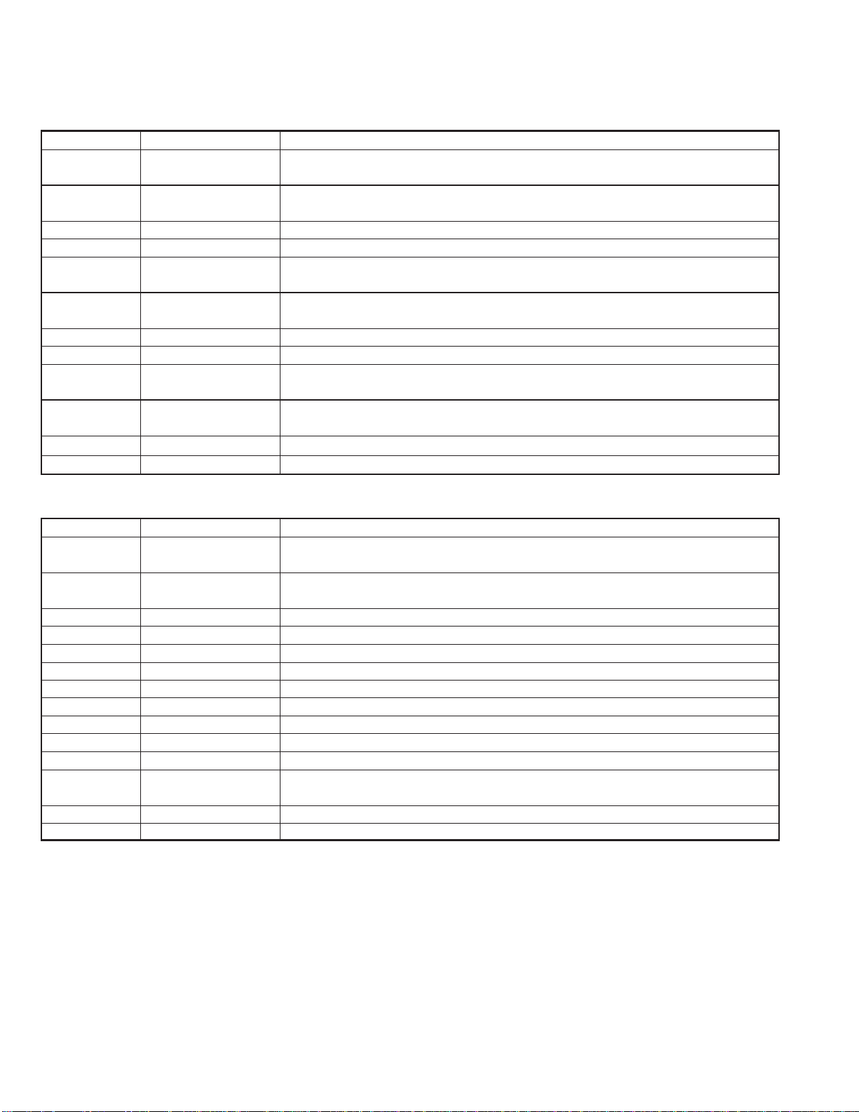
UX-510UA
FO-1470U
[4] Error code table
1. Communication error code table
G3 Transmission
Code Final received signal Error Condition (Receiver side)
0 Incomplete signal frame Cannot recognize bit stream after flag
1 NSF, DIS Cannot recognize DCS signal by echo etc.
Cannot recognize NSS signal (FIF code etc)
2 CFR Disconnects line during reception (carrier missing etc)
3 FTT Disconnects line by fall back
4 MCF Disconnects line during reception of multi page
Cannot recognize NSS, DCS signal in the case of mode change
5 PIP or PIN The line is hung up without replying to telephone request from the receiving party.
6 RTN or RTP Cannot recognize NSS, DCS signal after transmit RTN or RTP signal.
7 No signal or DCN No response in receiver side or DCN signal received* (transmitter side)
8 − Owing to error in some page the error could not be corrected although the specified number of
error retransmissions were attempted.
11 − Error occurred after or while reception by the remote (receiving) machine was revealed to be
impossible.
12 − Error occurred just after fallback.
13 − Error occurred after a response to retransmission end command was received.
G3 Reception
Code Final received signal Error Condition (Receiver side)
0 Incomplete signal frame Cannot recognize bit stream after flag
1 NSS, DCS Cannot recognize CFR or FTT signal
Disconnects line during transmission (line error)
2 NSC, DTC Cannot recognize NSS signal (FIF code etc)
3 EOP Cannot recognize MCF, PIP, PIN, RTN, RTP signal
4 EOM Cannot recognize MCF, PIP, PIN, RTN, RTP signal in the case of mode change
5 MPS The line is hung up without replying to communication request.
6 PR1-Q Cannot recognize PIP, PIN signal in the case of TALK request
7 No signal or DCN No response in transmitter (cannot recognize DIS signal) or DCN signal received* (receiver side)
8 − Error occurred upon completion of reception of all pages.
9 − Error occurred when mode was changed or Transmission/Reception switching was performed.
10 − Error occurred during partial page or physical page reception.
11 − Error occurred after or during inquiry from the remote (transmitting) machine as to whether
reception is possible or not.
12 − Error occurred during or just after fallback.
13 − Error occurred after the retransmission end command was received.
2 – 20
Page 33
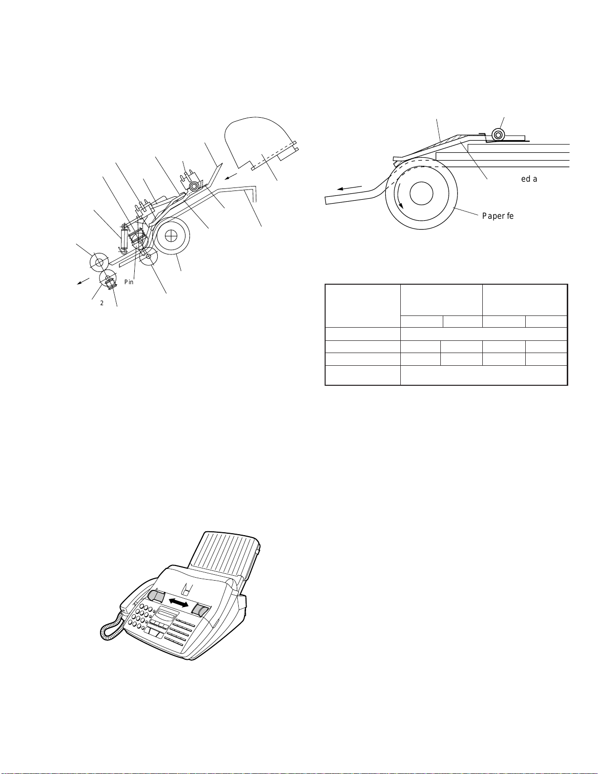
CHAPTER 3. MECHANISM BLOCKS
[1] General description
1. Document feed block and diagram
Document
guide upper
Front
sensor
Paper feed arm
Paper feed
spring
Hopper guide
Document guide
lower
Pinch roller
spring
Separate
spring
Feed roller 2
Original
sensor
Separation
rubber
Separate
plate
UX-510UA
FO-1470U
3-2. Automatic document feed
1) Use of the paper feed roller and separation rubber plate ensures
error-free transport and separation of documents. The plate spring
presses the document to the paper feed roller to assure smooth feeding of the document.
2) Document separation method: Separation rubber plate
Separation rubber
Fig. 3
Paper feed spring
Paper feed arm
Paper feed roller
Paper feed roller
Feed roller
Pinch roller2
Pinch roller
Pinch roller spring 2
Fig. 1
2. Document feed operation
1) The original, which is set in the document hopper, feeds automatically when the front sensor is activated. This in turn activates the
pulse motor which drives the document supply roller. The document
stops when the lead edge is detected by the document sensor.
2) The lead edge of the original is fed a specified number of pulses after
the lead edge of the document is detected for the reading process to
begin.
3) The trailing edge of the original is fed a specific number of pulses
after the trailing edge of the document deactivates the original sensor. The read process then stops and the original is discharged.
4) When the front sensor is in the OFF state (any document is not set
up in the hopper guide), the drive will be stopped when the document is discharged.
3. Hopper mechanism
3-1. General view
3-3. Documents applicable for automatic feed
4x6 series
(788mm x 1091mm x
1000 sheets)
Minimum Maximum Minimum Maximum
Feeder capacity 20 sheets, max.
Paper weight 45kg 64.3kg 52g/m274.3g/m
Paper thickness (ref.)
0.06mm 0.09mm 0.06mm 0.09mm
Paper size 128mm x 148mm ~ (MIN. SIZE)
A4 (210mm x 297mm), Letter (216mm x 279mm)
NOTE: Double-side coated documents and documents on facsimile re-
cording paper should be inserted manually. The document feed
quantity may be changed according to the document thickness.
Documents corresponding to a paper weight heavier than 64.3kg (74.3g/
m2 ) and lighter than 135kg (157g/m2 ) are acceptable for manual feed.
Documents heavier than 135kg in terms of the paper weight must be
duplicated on a copier to make it operative in the facsimile.
Square
meter series
3-4. Loading the documents
1) Make sure that the documents are of suitable size and thickness,
and free from creases, folds, curls, wet glue, wet ink, clips, staples
and pins.
2) Place documents face down in the hopper.
i) Adjust the document guides to the document size.
ii) Align the top edge of documents and gently place them into the
hopper. The first page under the stack will be taken up by the
feed roller to get ready for transmission.
NOTES: 1) Curled edge of documents, if any, must be straighten
out.
2) Do not load the documents of different sizes and/or
thicknesses together.
2
Fig. 2
The hopper section contains document guides that are used to adjust
the hopper to the width of the original document. This ensures that the
original feeds straight into the fax machine for scanning.
Document width: 148 mm to 216 mm (A5 longitudinal size to Letter
longitudinal size)
NOTE: Adjust the document guide after setting up the document.
3 – 1
Page 34
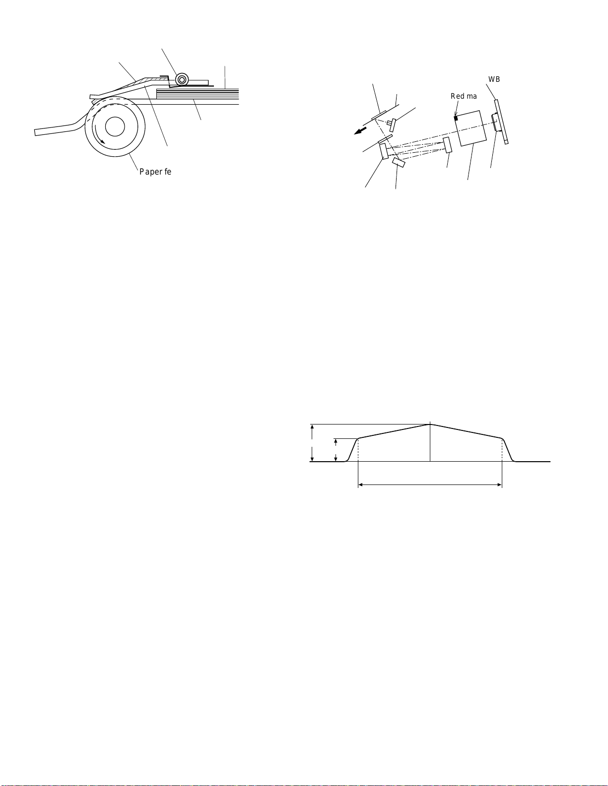
UX-510UA
,,
,
,
FO-1470U
Paper feed spring
Separation
rubber
Last page of document
First page of
document
Paper feed arm
Paper feed roller
Fig. 4
3-5. Documents requiring use of copy
1) Documents smaller than 128mm x 148mm.
2) Documents thinner than the thickness of 0.06mm.
3) Documents containing creases, folds, or curls, especially those whose
surface is curled (maximum allowable curl is 5mm).
4) Documents containing tears.
5) Carbon-backed documents. (Insert a white sheet of paper between
the carbon back and the document carrier to avoid transfer of carbon
to the carrier.)
6) Documents containing an easily separable writing material (e.g., those
written with a lead pencil).
7) Transparent documents.
8) Folded or glued documents.
4. Document release
5. Optical system
(1) General view
Reader
glass
Rear sheet
Mirror 3
Document
LED lamp
Mirror 2
Mirror 1
Fig. 5
CCD PWB
Red mark
CCD
Lens
(2) Composition
The optical system is composed of the document feed mechanism, the
LED lamp, the reflecting mirrors, the f ocusing lens, the CCD sensor , and
the read process circuit.
5-1. LED Lamp/Lens
The LED lamp is used to project light to the document.
NOTE: Take care for the position of the red mark on the lens. (Top of
the light-projected side)
5-2. CCD
The CCD (charge coupled device) image sensor consists of a photodiode
array which converts the intensity of light reflected from the document
surface into series of analog voltages which are then stored in an ana
log shift register. The series of analog v oltages are then converted into a
digital equivalent by a black/white binary logic circuit.
(Example) Scan signal output waveform
4-1. General
To correct a jammed document or to clean the document running surface, pull the operation panel lock lever under the front center of the
operation panel. To open the upper document guide, the operation panel
must be opened first.
Peak
100%
50%
minimum
Scan line
Maximum document width, 216mm
length
Fig. 6
1) The minimum output from the CCD at the maximum scan width of
document (216mm) must be more than 50% of the peak value.
2) The peak output must be about 0.2 ~ 0.6 under room temperature to
avoid CCD saturation.
3 – 2
Page 35
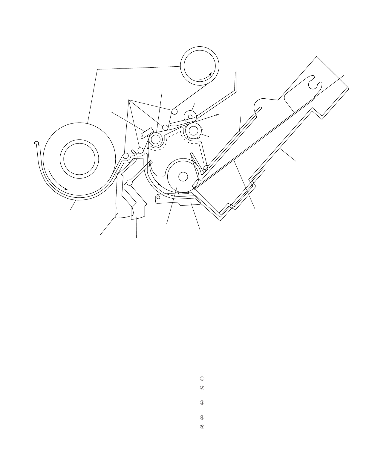
6. Recording block
(1) General view
UX-510UA
FO-1470U
Supply
side
Main frame
Imaging film
Thermal
head
Film sensor
lever
Guide shaft
P-IN sensor lever
Take-up
side
Platen
roller
Pinch
roller
Paper guide
PO roller
U turn guide
RP hopper
Rotation plate
PU roller
Separate plate
6-1. Driving
In the drive mechanism, the rotating force of the pulse motor for both
transmission and reception is transmitted to the paper supply roller, the
recording paper feed roller and imaging film drive gear through the pulse
motor axle gear, reduction gear and planetary gear.
6-2. Recording
This equipment employs the thermal transcription system which used
the thermal head imaging film.
1) Thermal head
The thermal head is composed of 2,016 heating elements in traverse
line, and the resolution power is 8 dots/mm. The maximum speed is 10
ms/line.
2) Structure of recording mechanism
Recording is achieved by applying a suitable pressure to the thermal
head through the imaging film of the recording paper feed roller and the
recording paper.
The main scanning is electronically done, and the sub-scanning is me
chanically done (by sending the recording paper with the recording paper feed roller).
Fig. 7
3) Recording paper transfer sequence
a) The recording paper stored in the RP hopper is fed with the PU roller,
and the recording paper is stopped when the P-IN sensor is turned
on by sensing its lead edge.
b) Hereafter, the imaging film and recording paper are transferred with
the recording paper feed roller, and thermal transcription is done on
the recording paper.
c) After thermal transcription, the imaging film is taken up by the roller
on the take-up side, and the recording paper is discharged by the PO
roller.
As basic, the density unevenness mainly results from the longitudinal misalignment of the thermal head to the heater line. Other-wise,
the head is in uneven contact with the recording paper f eed roller, or
the imaging film is wrinkled.
The following items are described as the simplified checking method.
1
Are the power and signal cables of the thermal head suitably treated?
2
Does the same symptom appear even if the thermal head pres-sure
spring is replaced?
3
Is the feed roller of the recording paper concentric? (Density is uneven at intervals.)
4
Does the same symptom appear even if the thermal head is replaced?
5
Is the imaging film stained or wrinkled?
3 – 3
Page 36
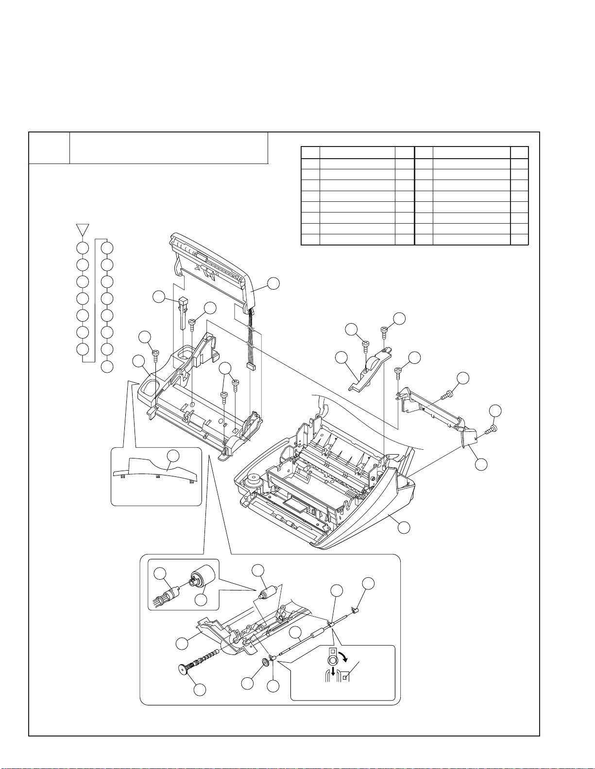
UX-510UA
FO-1470U
[2] Disassembly and assembly procedures
• This chapter mainly describes the disassembly procedures. For the assembly procedures, reverse the disassembly procedures.
• Easy and simple disassembly/assembly procedures of some parts and units are omitted. For disassembly and assembly of such parts and units,
refer to the Parts List.
• The numbers in the illustration, the parts list and the flowchart in a same section are common to each other.
• To assure reliability of the product, the disassembly and the assembly procedures should be performed carefully and deliberately.
2
Parts list (Fig. 1)
No. Part name Q’ty No. Part name Q’ty
1 Mechanism unit 1
2 Operation panel unit 1
3 Screw (3×12) 2
4 Side cover 1
5 Screw (3×12) 1
6 Screw (3×10) 2
7 Rear cabinet 1
8 Screw (3×10) 4
9 Hook switch lever 1
10
Document guide lower unit
11 Transfer gear 1
12 Transfer bearing 3
13 Transfer roller 1
14 Feed gear ass’y 1
15 Paper feed roller 1
16 Document guide lower 1
3
3
4
5
1
1
Operation panel unit, document guide
lower and rear cover
1
2
9
3
10
4
11
10
9
8
8
8
5
12
6
13
7
14
8
15
16
6
6
10
Hook the three lock nail
to LOWER CABINET.
14
16
15
14
11
15
13
12
An attachment rib is attached
in accordance with hole.
Fig. 1
12
7
1
12
Rib
3 – 4
Page 37
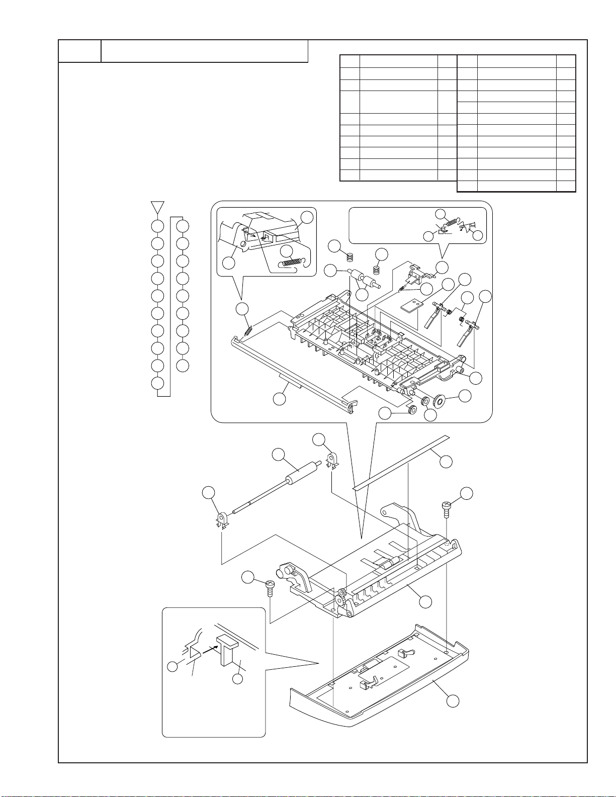
UX-510UA
FO-1470U
2
Document guide upper
1
20
2
12
3
13
4
14
5
15
6
16
7
17
8
18
5
4
4
Parts list (Fig. 2)
No. Part name Q’ty No. Part name Q’ty
1 Operation panel unit 1
2 Screw (3×10) 2
3 Document guide upper 1
unit
4 Panel lock lever spring 1
5 Panel lock lever 1
6 Idler gear (28Z) 1
7 Idler gear (20Z) 1
8 Transfer gear 2 1
9 Rear sheet 1
After mounting to the
fulcrum and push down
to the direction of arrow
mark.
20
10 Transfer bearing 2
11 Transfer roller 1
12 Separate spring 1
13 Separate plate 1
14 Paper feed arm 2
15 Paper feed spring 1
16 Separation rubber 1
17 Pinch roller spring 2
18 Pinch roller shaft 1
19 Pinch roller 2
20 Document guide upper 1
12
13
17
17
12
13
16
14
15
14
18
19
10
11
9
19
20
20
5
8
7
6
10
11
10
9
2
2
3
Positioning rib
3
Hook
1
A hook of a document
guide upper is fit to
positioning rib of panel
unit .
1
Fig. 2
3 – 5
Page 38
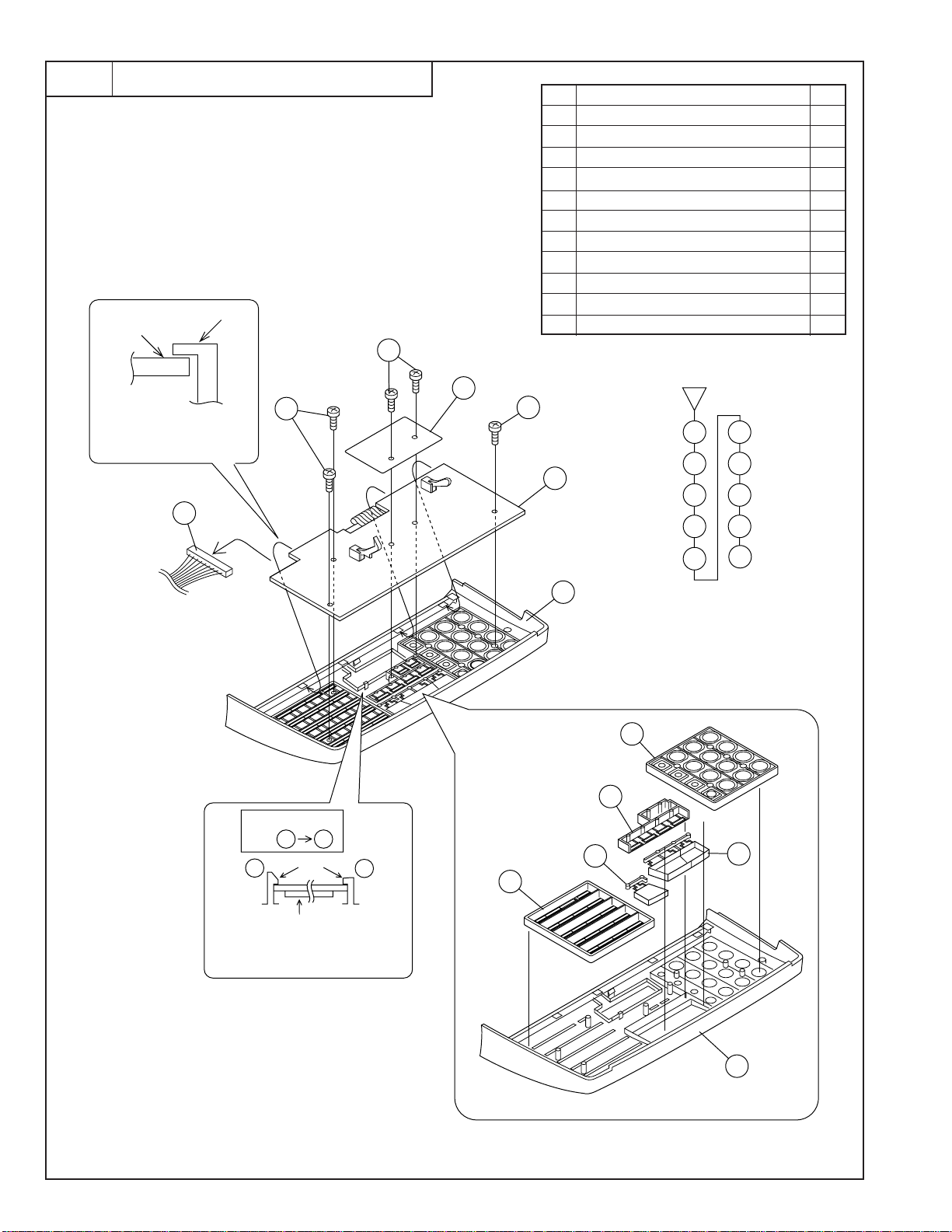
UX-510UA
FO-1470U
3
Operation panel
Panel PWB
Note) Keep the panel PWB
to under the rib like a
picture.
10
rib
Parts list (Fig. 3)
No. Part name Q’ty
1 Operation panel unit 1
2 Screw (2.6×6) 5
3 Insulation sheet 1
4 Operation panel PWB unit 1
5 12 key 1
6 Start key 1
7 Stop key 1
8 Mode key 1
9 Direct key 1
10 Panel cable 1
11 Operation panel 1
2
3
2
2
1
2
3
7
8
4
4
9
5
10
Ass'y process
a b
b
Note) The LCD PWB should be securely
locked by the click of the panel
case.
Rib
LCD PWB
a
11
6
1
5
8
7
6
9
Fig. 3
3 – 6
11
Page 39
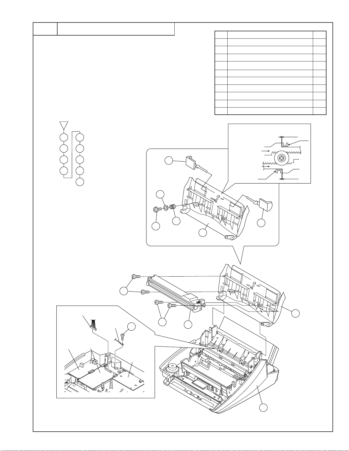
UX-510UA
FO-1470U
4
Top cover and head frame unit
1
2
6
7
3
4
8
5
9
6
Parts list (Fig. 4)
No. Part name Q’ty
1 Mechanism unit 1
2 Top cover unit 1
3 Screw (3×10) 5
4 Head frame unit 1
5 Hopper guide, right 1
6 Hopper guide, left 1
7 Screw (3×6) 1
8 Pinion gear 1
9 Hopper spring 1
10 Top cover 1
Confirm of HOPPER GUIDE position.
GAP 0
Rib
HOPPER GUIDE,
LEFT
HOPPER GUIDE,
RIGHT
Rib
GAP 0
10
HEAD CABLE
TEL/LIU
PWB
CONTROL
PWB
HEAD
EARTH
CABLE
3
3
POWER
SUPPLY
PWB
8
7
9
5
10
2
3
4
Fig. 4
3 – 7
1
Page 40
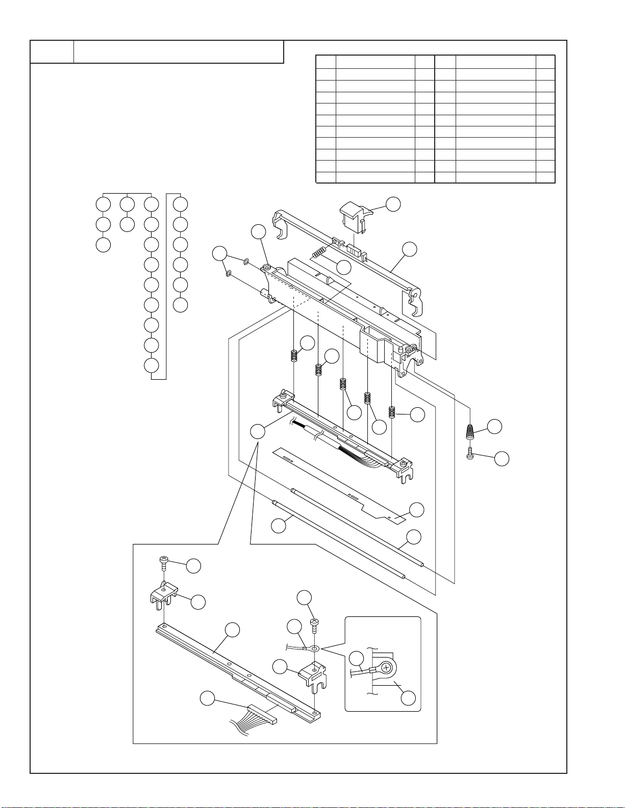
UX-510UA
FO-1470U
5
Head frame and thermal head
124
3
6
15
7
5
16
8
17
13
6
9
18
10
19
11
20
Parts list (Fig. 5)
No. Part name Q’ty No. Part name Q’ty
1 Release knob 1
2 Lock spring 1
3 Lock lever 1
4 Screw (3×10) 1
5 Pop up spring 1
6 Cut washer 2
7 Film guide shaft 2
8 Head guide sheet 1
9 Thermal head unit 1
10 Head spring B 2
11 Head spring 2 2
12 Head spring 1 1
13 Head frame 1
14 Head cable 1
15 Screw (3×6) 1
16 Head earth cable 1
17 Head guide, right 1
18 Screw (3×6) 1
19 Head guide, left 1
20 Thermal head 1
1
3
2
12
13
11
10
14
18
19
14
20
12
9
10
11
5
4
8
7
7
15
16
Fix position of
EARTH CABLE.
16
17
17
Fig. 5
3 – 8
Page 41
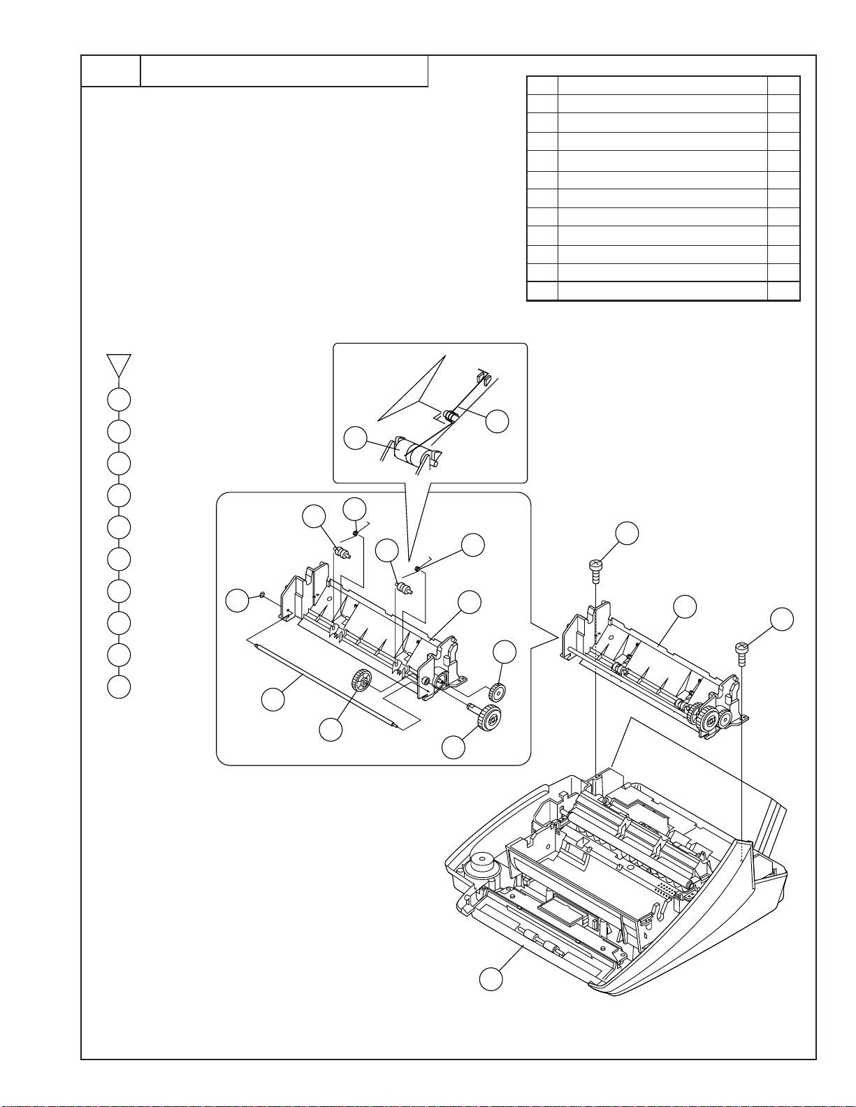
UX-510UA
FO-1470U
6
Paper out guide
Parts list (Fig. 6)
No. Part name Q’ty
1 Mechanism unit 1
2 Screw (3×10) 2
3 Paper out guide unit 1
4 Idler gear A 1
5 Take-up gear 1
6 Slip gear ass’y 1
7 Cut washer 1
8 Film shaft C 1
9 PO pinch roller spring 2
10 PO pinch roller 2
11 Paper out guide 1
1
2
3
10
9
4
5
6
7
8
9
10
11
10
9
2
11
9
3
10
7
2
4
8
5
6
Fig. 6
3 – 9
1
Page 42
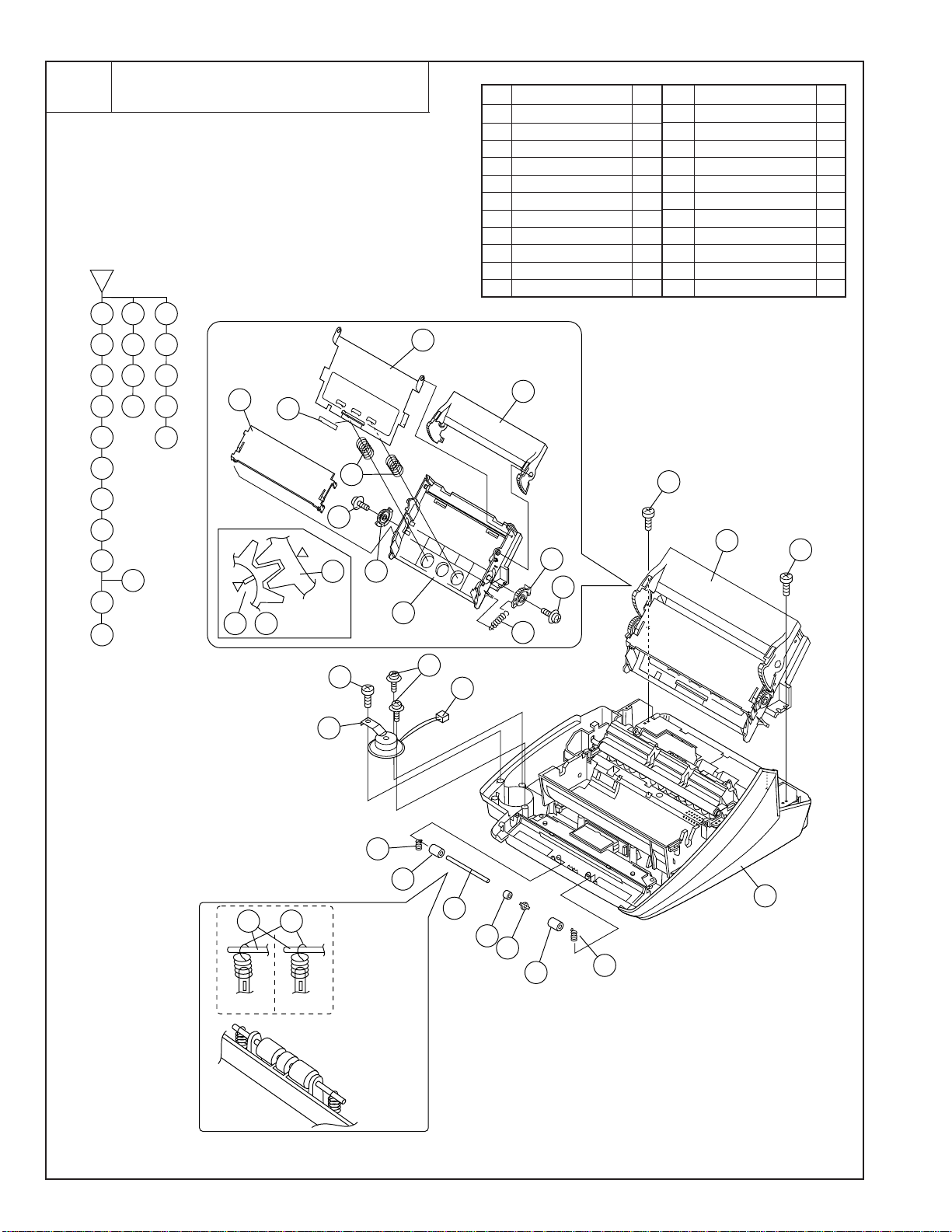
UX-510UA
FO-1470U
7
Recording paper hopper, speaker and
pinch roller
1
2
14
18
3
15
19
4
16
20
5
17
21
6
22
7
4
11
12
10
Parts list (Fig. 7)
No. Part name Q’ty No. Part name Q’ty
1 Mechanism unit 1
2 Screw (3×12) 2
3 RP hopper unit 1
4 Paper guide 1
5 Screw 2
6 RP release spring 1
7 RP release gear, right 1
8 RP release gear, left 1
9 RP release plate 1
10 Paper up plate 1
11 RP pad 1
12 Cassette spring 2
13 RP hopper 1
14 Screw 2
15 Screw (3×10) 1
16 Speaker holder spring 1
17 Speaker 1
18 Pinch roller spring 2
19 Pinch roller 2
20 Document kick plate 1
21 Document kick roller 1
22 Pinch roller shaft 1
9
2
8
5
10
12
13
9
7
5
6
11
7 ,
8
9
8
13
3
2
20
15
16
18
OKOK
Position of pinch
shaft,roller,spring
18
19
14
22
17
21
20
19
1
18
Fig. 7
3 – 10
Page 43
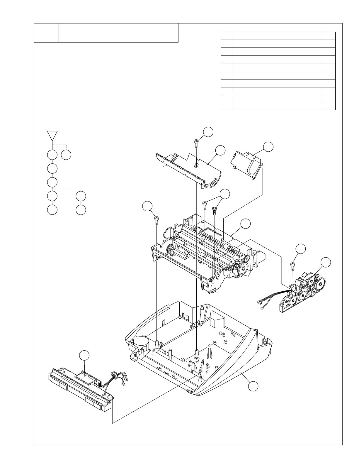
UX-510UA
FO-1470U
2
3
Parts list (Fig. 8)
No. Part name Q’ty
1 Mechanism unit 1
2 Screw (3×10) 1
3 ROM cover 1
4 Memory cover 1
5 Screw (3×10) 1
6 Drive unit 1
7 Screw (3×10) 3
8 Main frame unit 1
9 Optical unit 1
4
8
Main frame unit, ROM cover, memory
cover, drive unit and optical unit
1
2
4
3
7
8
9
5
6
7
7
8
5
6
9
1
Fig. 8
3 – 11
Page 44
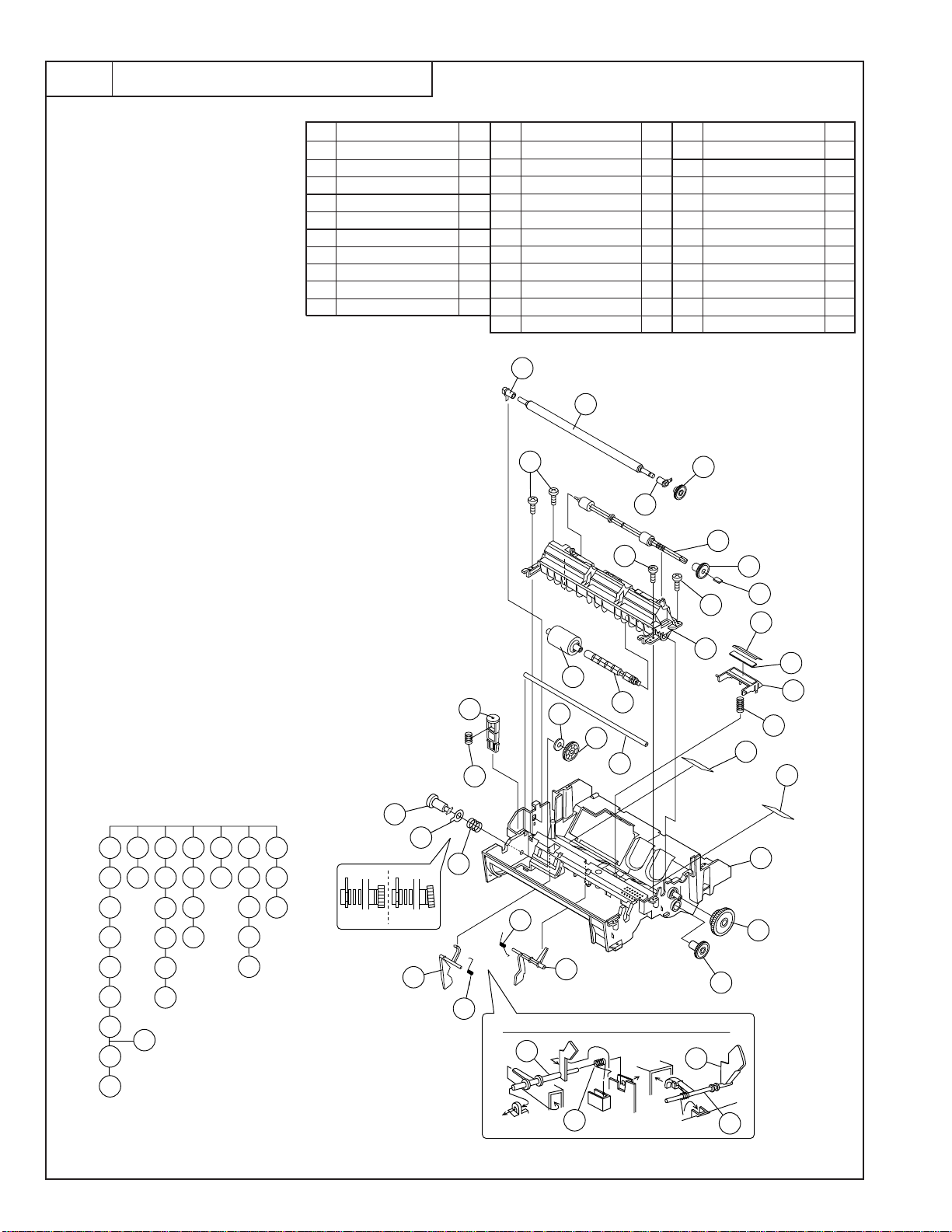
UX-510UA
FO-1470U
9
Main frame, U turn guide and transfer roller etc.
Parts list (Fig. 9)
No. Part name Q’ty No. Part name Q’ty No. Part name Q’ty
1 Reduction gear A 1
2 PU gear 1
3 Platen bearing 1
4 Platen gear 1
5 Platen bearing 1
6 Platen roller 1
7 PO gear 1
8 Screw (3×10) 4
9 Film guide shaft B 1
10 PU roller shaft 1
11 PU roller ass’y 1
12 PO roller ass’y 1
13 U turn guide 1
14 Sensor lever spring 1
15 Film sensor lever 1
16 Sensor lever spring 1
17 P-IN sensor lever 1
18 Pop up spring 1
19 Cover switch lever 1
20 Back tension gear 1
21 Back tension felt 1
22 Slip spring 1
23 Hold down plate B 1
24 Back tension stopper 1
25 Separate plate spring 1
26 Separate sheet 1
27 Separate plate sheet 1
28 Separate plate 1
29 Guide sheet, left 1
30 Guide sheet, right 1
31 PO gear cushion 1
32 Main frame 1
5
6
8
4
3
1
2
3
4
5
6
7
8
101112
13
25
26
27
28
31
14
1819202129
15
16
17
22
23
24
30
32
24
OK NG
15
23
22
14
8
11
19
21
10
20
9
18
16
17
Position of SENSOR LEVER and SPRING.
17
15
13
8
12
7
31
26
27
28
25
29
30
32
1
2
9
16
Fig. 9
14
3 – 12
Page 45
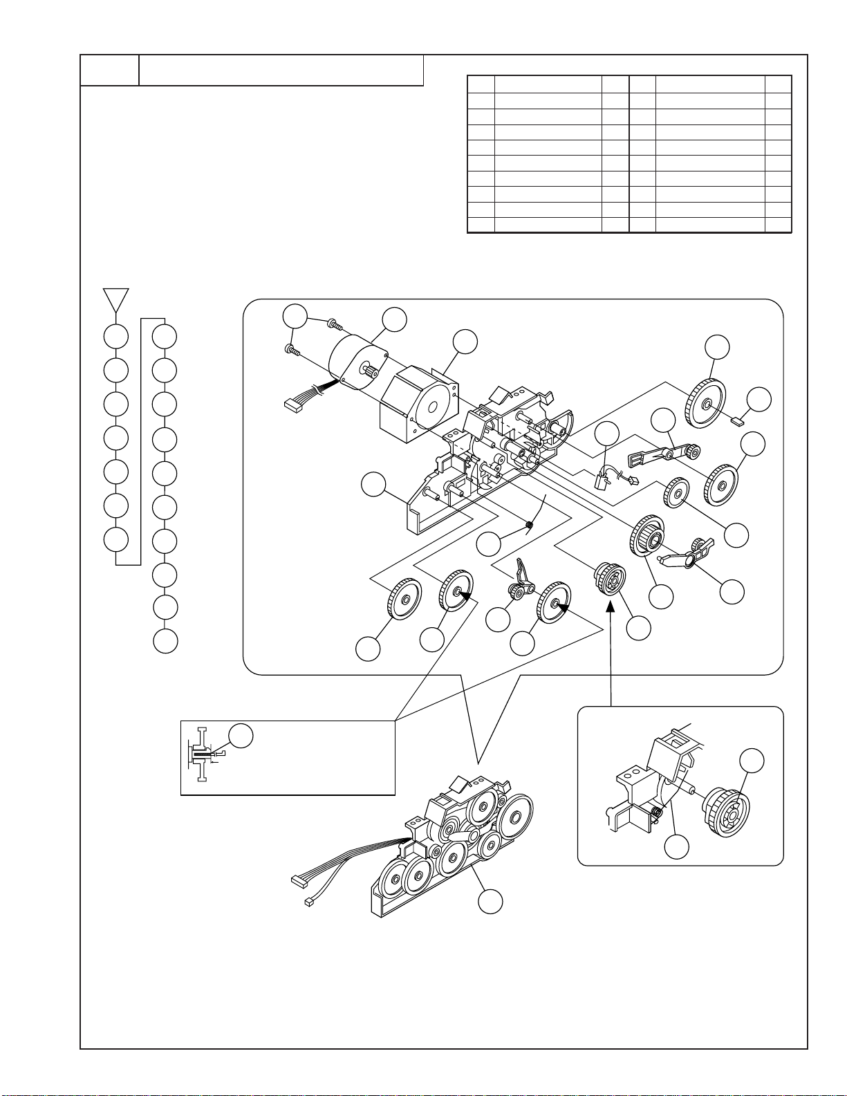
UX-510UA
FO-1470U
10
1
2
3
4
5
Drive unit frame
9
10
11
12
13
14
Parts list (Fig. 10)
No. Part name Q’ty No. Part name Q’ty
1 Drive unit 1
2 Reduction gear B 1
3 Planet lever B ass’y 1
4 Idler gear A 1
5 Idler gear C 1
6 Reduction gear A 1
7 Planet lever C ass’y 1
8 Cam hold spring 1
9 Cam A 1
15
10 Planet lever A ass’y 1
11 Reduction gear C 2
12 Cam switch ass’y 1
13 Screw (3×10) 2
14 Motor 1
15 Motor heat sink 1
16 Cushion 1
17 Band 2
18 Drive unit frame 1
2
7
12
16
5
6
7
8
13
14
15
18
8
4
16
3
17
18
11
11
10
6
9
5
17
Cut after insert must be
9
touch to the bottom.
8
Fig. 10
3 – 13
1
Page 46
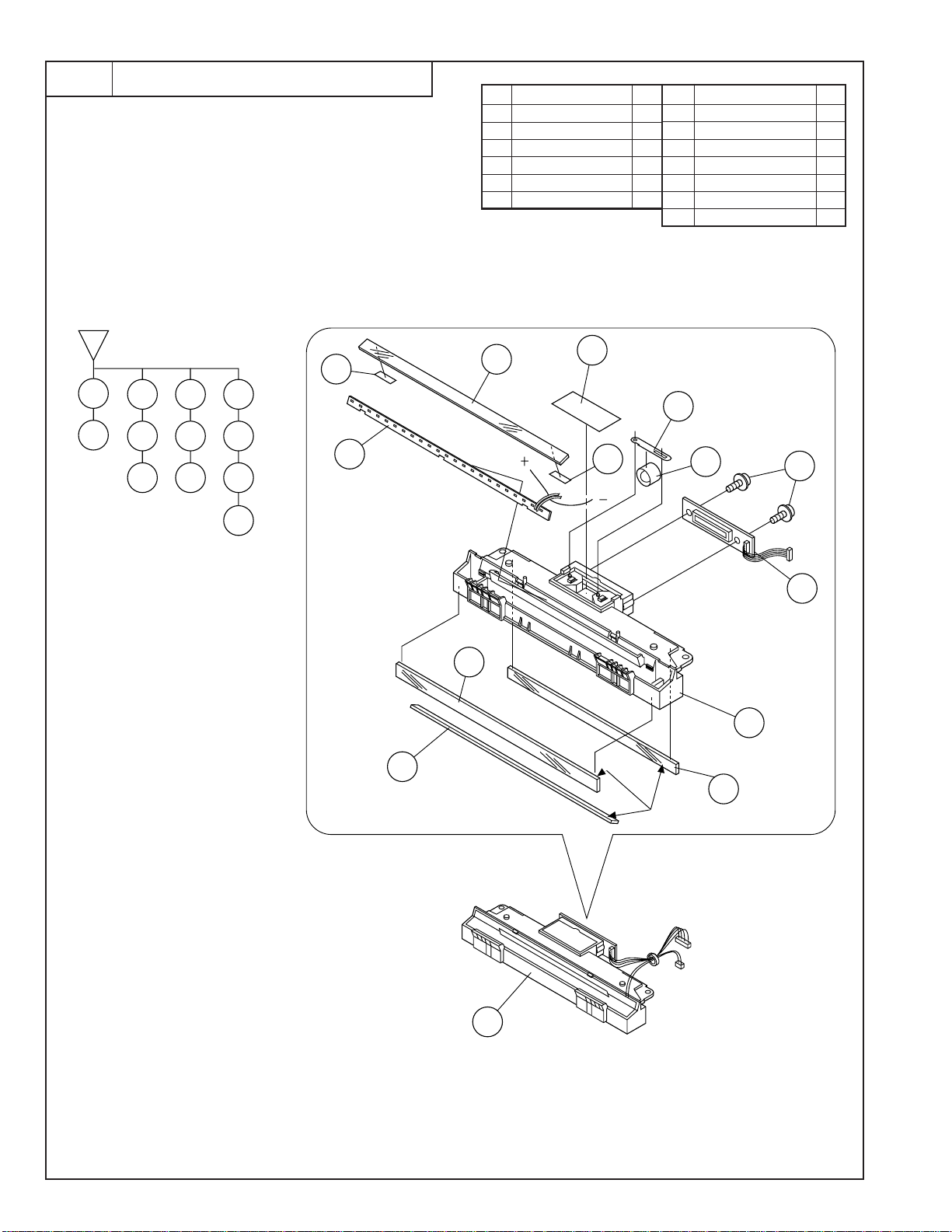
UX-510UA
FO-1470U
11
Optical frame
1
2
3
Parts list (Fig. 11)
No. Part name Q’ty No. Part name Q’ty
1 Optical unit 1
2 Screw 2
3 CCD PWB unit 1
4 Shading sheet 1
5 Lens holding spring 1
6 Lens 1
9
4
5
7
10
8
11
8
6
9
12
7
Red( )
4
9
Blue
( )
7 Reader glass 1
8 LED 1
9 Shading sheet 3 2
10 Mirror 3 1
11 Mirror 1 1
12 Mirror 2 1
13 Optical frame 1
5
6
2
13
11
3
10
13
12
Face of reflect
1
Fig. 11
3 – 14
Page 47
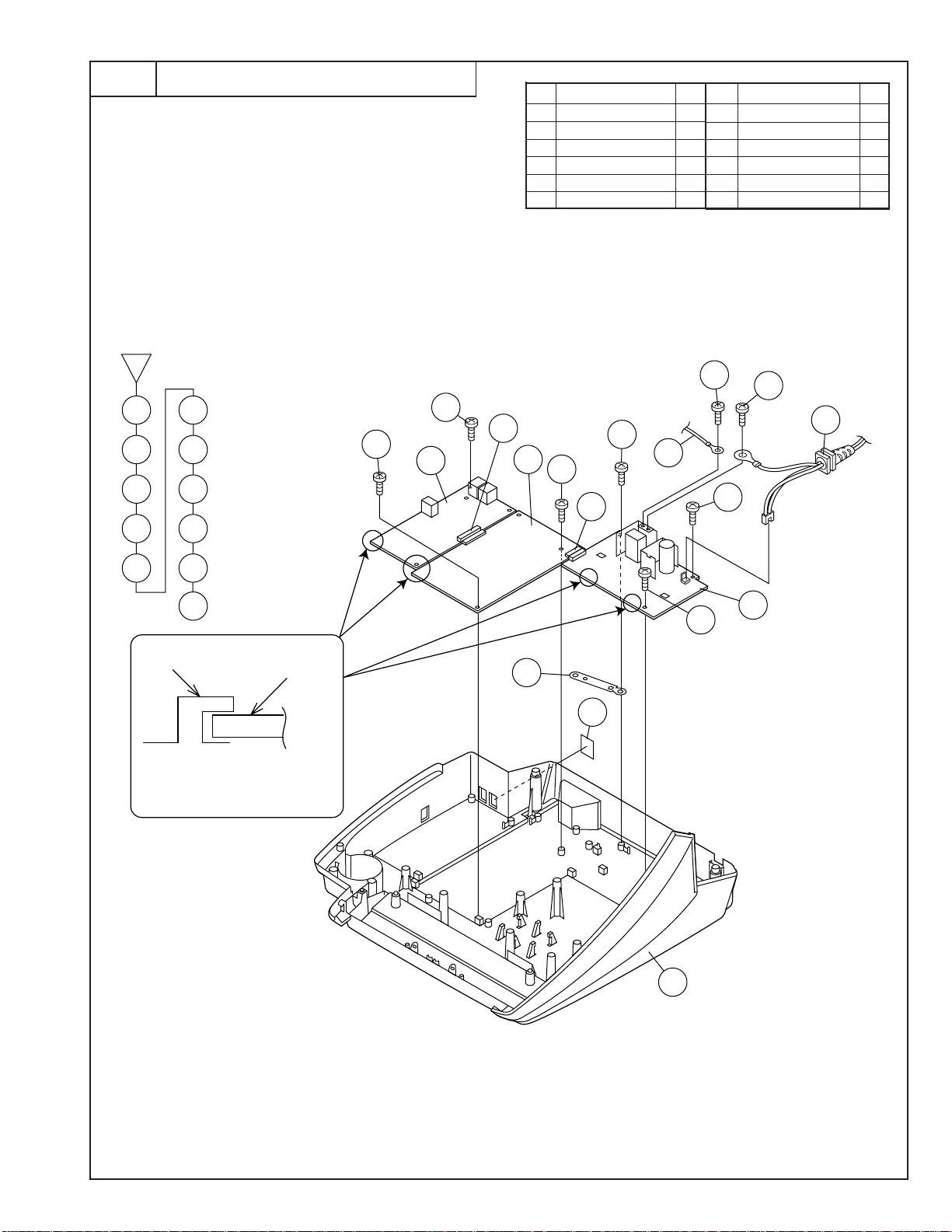
UX-510UA
FO-1470U
12
PWB section
1
2
3
4
5
7
8
9
10
Parts list (Fig. 12)
No. Part name Q’ty No. Part name Q’ty
1 Mechanism unit 1
2 Screw (3×6) 1
3 TEL/LIU ARG cable 1
4 Screw (4×6) 1
5 AC cord 1
6 Screw (3×10) 6
7 Connector 2
8 Control PWB unit 1
9 TEL/LIU PWB unit 1
10 Power supply PWB unit 1
11 Earth plate 1
12 Jack sheet 1
2
4
6
7
6
9
8
6
6
3
7
6
5
6
11
12
Hook
Note) The PWB hook to
cabinet.
PWB
10
6
11
12
1
Fig. 12
3 – 15
Page 48
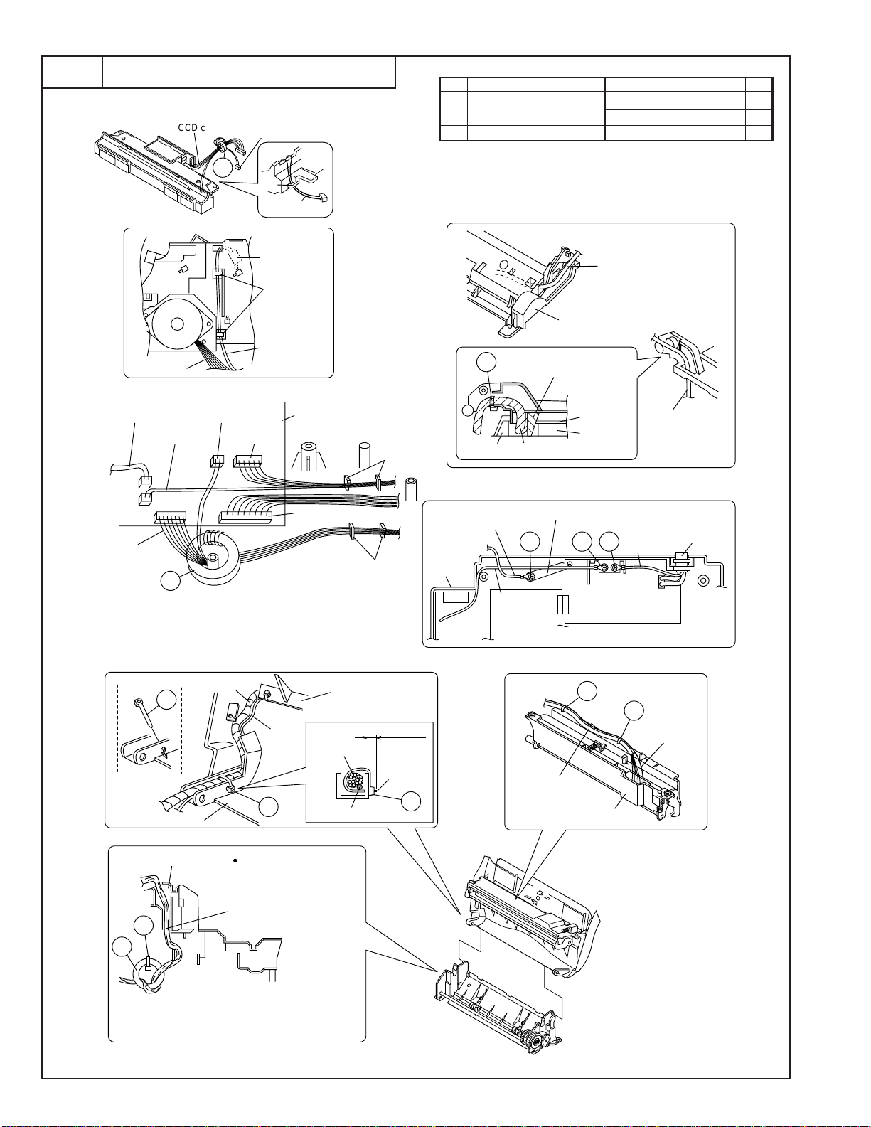
UX-510UA
FO-1470U
13
Wire treatment
CCD cable
Motor cable
Speaker
cable
Cam switch
cable
2
LED
cable
LED cable
Rib
Cam switch
Rib
Cam switch
cable
Motor
cable
LED
cable
Control PWB
Rib
Parts list (Fig. 13)
No. Part name Q’ty No. Part name Q’ty
1 Band (Black) 1
2 Core (F2125) 2
3 Screw (3×6) 1
Document guide lower
1
Document guide upper rib
Panel rib
Panel cable
4 Screw (4×6) 1
5 Screw (3×10) 2
6 Band (100mm) 5
Panel cable
Panel PWB
Key
Panel cable
CCD
cable
2
PO guide
6
2
The CCD and LED cables
pass to the core 3 times.
Head cable
6
Top cover
Panel cable
Head
earth
Head cable
cable
6
Wiring position of
head and head earth cable.
Head and Head eart cable
Head earth cable
Head unit
Rib
within 5mm
Position of
BINDING
BAND head.
Lower
cabinet
TEL/LIU
PWB
Head earth
cable
Earth plate
5
ARG cable
Control
PWB
3
Power supply PWB
earth cable
AC cord
4
AC cord
6
6
Head earth
cable
Head cable
6
Head unit
The head and head
earth cables pass to
the core 3 times.
Fig. 13
3 – 16
Page 49
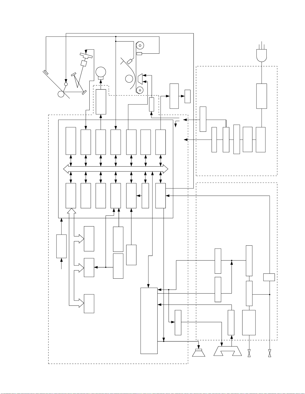
CHAPTER 4. DIAGRAMS
SRAM
256kbit
ROM
2Mbit
CPU
CPU I/F
TIMER
RTC
PIO
WATCHDOG
TIMER
CLOCK
32.768kHz
INTERRUPT
CONTROLLER
CCD I/F
MOTOR I/F
SENSOR I/F
SIO
THERMAL
HEAD I/F
PANEL I/F
OPERATION
PANEL
CONTROL PWB UNIT
1CHIP FAX ENGINE (SCE114)
HANDSET
SPEAKER
+5V +24V
OPERATION
PANEL
TEL/LIU
PWB UNIT
DRIVER
PM
POWER SUPPLY
PWB UNIT
DRAM
4Mbit
REGULATOR
AMPLIFIER
RESET
VOLTAGE
REGULATOR
+3.3V
+5V
AMPLIFIER
AMPLIFIER
SURGE
PROTECT/
FILTER
CML TRANSFORMER
CI
VBT
STABILIZER
RECTIFIER
TRANSFORMER
RECTIFIER
DIODE
LINE
EXT.TEL
AMPLIFIER
BZ
CLOCK
32.256MHz
INTEGRATED ANALOG DEVICE
(20415)
LCD
RELAY
THERMAL
HEAD
P-IN
SENSOR
FILM
SENSOR
IMAGING
FILM
RECORDING PAPER
CCD
LED
FILTER
SURGE
ABSORBER
UX-510UA
FO-1470U
[1] Block diagram
4 – 1
Page 50
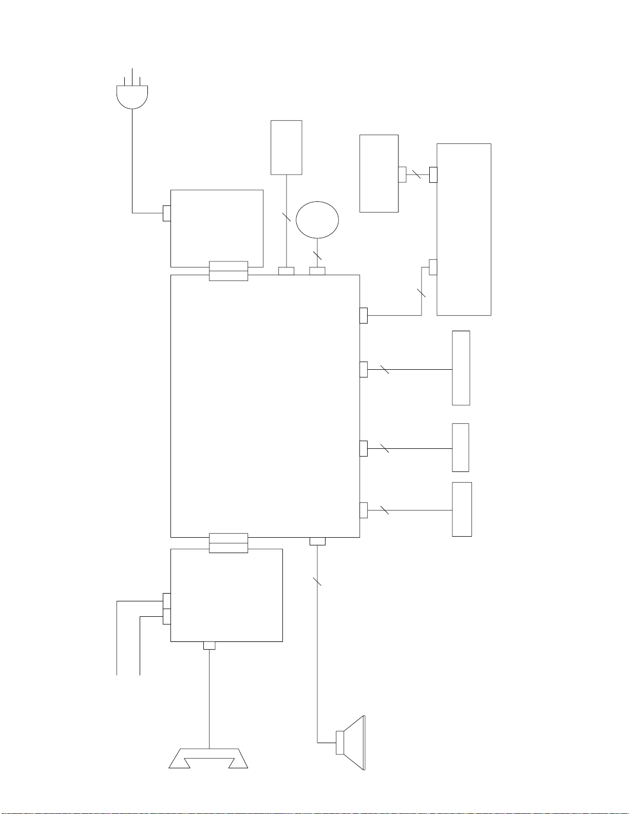
UX-510UA
AC CORD
SPEAKER
2
CNSP
CNHJ
HANDSET
TEL LINE
EXTERNAL LINE
TEL/LIU PWB
UNIT
CNLIUA
POWER
SUPPLY
PWB
14
CNCCD
CNLIUA
CONTROL PWB UNIT
CNPW
7
CNTH
OPERATION
PANEL PWB
LCD UNIT
14 6
THERMAL HEAD
CNPN
15
CCD PWB
CNLED
2
CN2
16
LED ARRAY
CNPN CNLCD
2
6
CAM SW.
TX/RX
MOTOR
CNCS
CNMT
CNLNJ
FO-1470U
[2] Wiring diagram
4 – 2
Page 51
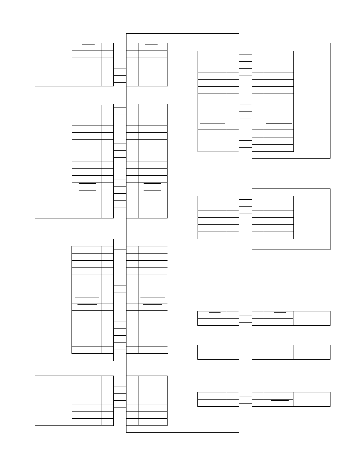
[3] Point-to-point dia gram
TX/RX
MOTOR
THERMAL
HEAD
OPERATION
PANEL
PWB
CCD PWB
TPBD
TPAD
TPBD
TPAD
VMT
VMT
VTH
VTH
STRB1
STRB2
THI
N.C.
THG
THG
THG
THVDD
STRB3
STRB4
LATCH
PCLK
DATA
VTH
KEN4A
KEN3A
KEN2A
KEN1A
DG
DG
+5V
ORGSNS
FRSNS
E
SEN4
SEN3
SEN2
SEN1
SEN0
VO
VCCD
VG
øT
ø2
ø1
øR
1
2
3
4
5
6
1
2
3
4
5
6
7
8
9
10
11
12
13
14
15
16
CNPN CNPN
1
2
3
4
5
6
7
8
9
10
11
12
13
14
15
1
2
3
4
5
6
7
CNMT
1
2
3
4
5
6
CNTH
1
2
3
4
5
6
7
8
9
10
THVDD
11
12
13
14
15
16
1
2
3
4
5
6
7
8
ORGSNS
9
10
11
12
13
14
15
CNCCD
1
2
3
4
5
6
7
TPBD
TPAD
TPBD
TPAD
VMT
VMT
VTH
VTH
STRB1
STRB2
THI
N.C.
THG
THG
THG
STRB3
STRB4
LATCH
PCLK
DATA
VTH
KEN4A
KEN3A
KEN2A
KEN1A
DG
DG
+5V
FRSNS
E
SEN4
SEN3
SEN2
SEN1
SEN0
VO
VCCD
VG
øT
ø2
ø1
øR
CONTROL
PWB
PE1
TEL OUT
TEL IN
TEL MUTE
CI
HS
CML
TXOUT
RXIN
RHS
DOOR SW
+5V
DG
+24VA
CNPW
+24V
+24V
MG
MG
+5V
DG
CNCSW
CSW
DG
CNSP
SP+
SP-
CNLED
+24V
LEDON
10
11
12
13
14
1
2
3
4
5
6
UX-510UA
FO-1470U
CNLIUACNLIUA
1
2
3
4
5
6
7
8
9
1
2
1
2
1
2
1
2
3
4
TEL MUTE
5
6
7
8
9
10
11
DOOR SW
12
13
14
CN2
1
2
3
4
5
6
1
2
1
2
1
2
N.C.
TEL OUT
TEL IN
CI
N.C.
CML
TXOUT
RXIN
RHS
+5V
DG
+24V
+24V
+24V
MG
MG
+5V
DG
CSW
DG
SP+
SP-
+24V
LEDON
TEL/LIU
PWB
POWER
SUPPLY
PWB
CAM
SWITCH
SPEAKER
LED
4 – 3
Page 52
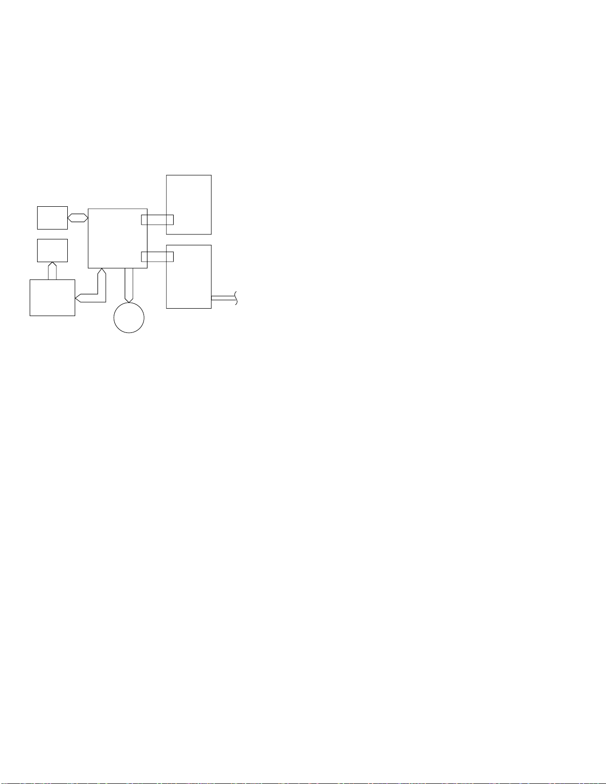
UX-510UA
FO-1470U
CHAPTER 5. CIRCUIT DESCRIPTION
[1] Circuit description
1. General description
The compact design of the control PWB is obtained by using CONEXANT
fax engine in the main control section and high density printing of surface mounting parts. Each PWB is independent according to its function
as shown in Fig. 1.
2. PWB configuration
TEL/LIU
PWB
CIS
CONTROL
LCD
PWB
PANEL
PWB
1) Control PWB
The control PWB controls peripheral PWBs, mechanical parts, transmission, and performs overall control of the unit.
This machine employs a 1-chip modem (SCE114) which is in-stalled on
the control PWB.
2) TEL/LIU PWB
This PWB controls connection of the telephone line to the unit.
3) Power supply PWB
This PWB provides voltages of +5V and +24V to the other PWBs.
4) Panel PWB
The panel PWB allows input of the operation keys.
PWB
POWER
SUPPLY
PWB
AC CORD
MOTOR
Fig. 1
3. Operational description
Operational descriptions are given below:
• Transmission operation
When a document is loaded in standby mode, the state of the document sensor is sensed via the 1 chip fax engine (SCE114). If the
sensor signal was on, the motor is started to bring the document into
the standby position. With depression of the START key in the offhook state, transmission takes place.
Then, the procedure is sent out from the modem and the motor is
rotated to move the document down to the scan line. In the scan
processor, the signal scanned by the CCD is sent to the internal image processor and the AD converter to convert the analog signal into
binary data. This binary data is transferred from the scan processor
to the image buffer within the RAM and encoded and stored in the
transmit buffer of the RAM. The data is then converted from parallel
to serial form by the modem where the serial data is modulated and
sent onto the line.
• Receive operation
There are two ways of starting reception, manual and automatic.
Depression of the START key in the off-hook mode in the case of
manual receive mode, or CI signal detection by the LIU in the automatic receive mode.
First, the SCE114 controls the procedure signals from the modem to
be ready to receive data. When the program goes into phase C, the
serial data from the modem is converted to parallel form in the modem interface of the 1 chip fax engine (SCE114) which is stored in
the receive buffer of the RAM. The data in the receive buffer is decoded software-wise to reproduce it as binary image data in the image buffer. The data is DMA transferred to the recording processor
within the SCE114 which is then converted from parallel to serial
form to be sent to the thermal head. The data is printed line by line by
the SCE114 which is assigned to control the motor rotation and strobe
signal.
• Copy operation
T o mak e a cop y on this facsimile , the COPY ke y is pressed when the
machine is in stand-by with a document on the document table and
the telephone set is in the on-hook state.
First, depression of the COPY key advances the document to the
scan line. Similar to the transmitting operation, the image signal from
the CCD is converted to a binary signal in the DMA mode via the 1
chip fax engine (SCE114) which is then sent to the image buffer of
the RAM. Next, the data is transferred to the recording processor in
the DMA mode to send the image data to the thermal head which is
printed line by line. The copying takes place as the operation is repeated.
5) LCD PWB
This PWB controls the LCD display.
6) CCD PWB
This PWB controls the pickup optical device.
5 – 1
Page 53
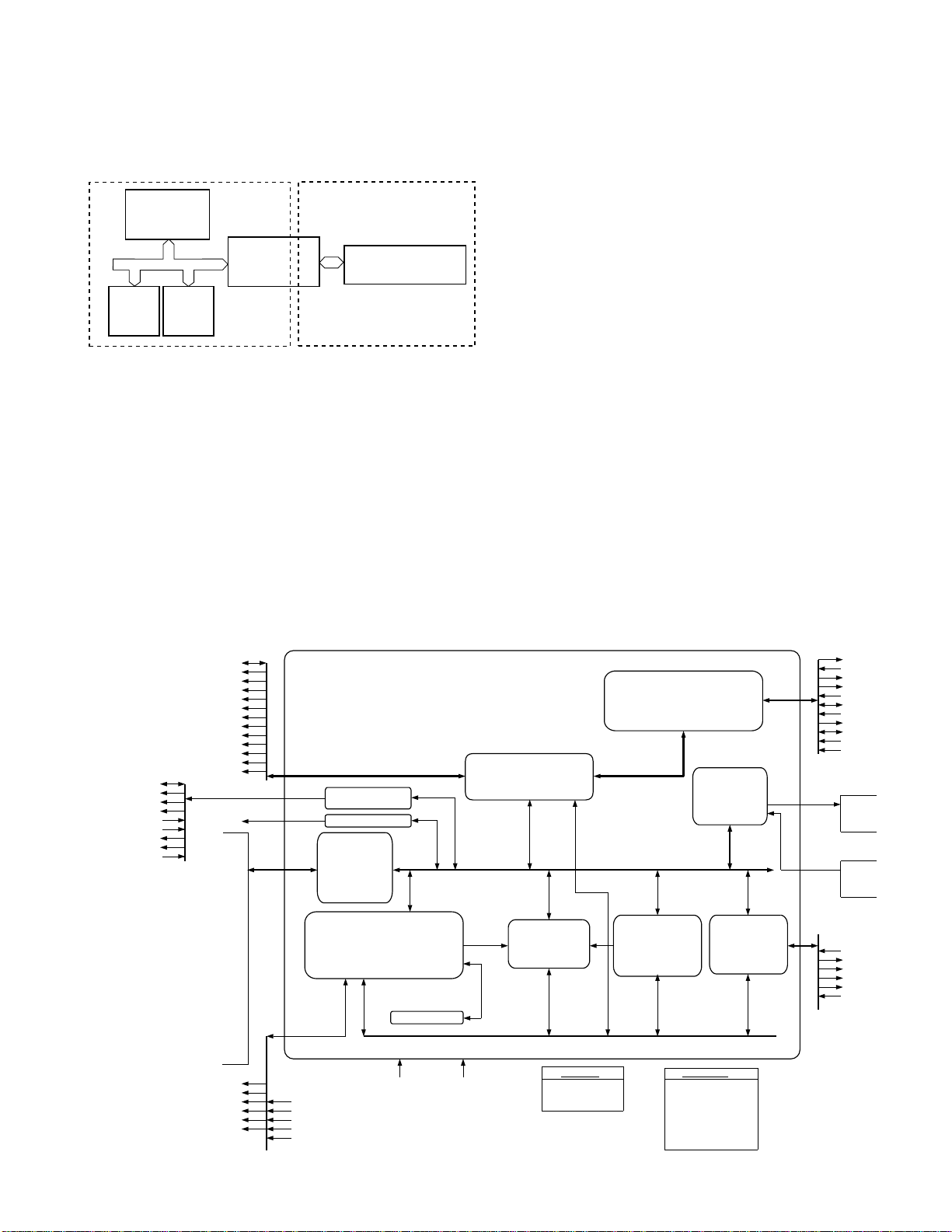
[2] Circuit description of control PWB
1. General description
Fig. 2 shows the functional blocks of the control PWB, which is composed of 5 blocks.
MAIN CONTROL BLOCK MODEM BLOCK
(3) ROM
(1) SCE114
(2) INTEGRATED
ANALOG (20415)
UX-510UA
FO-1470U
3) 27L2000 (IC4): pin-32 DIP (ROM)
ROM of 2Mbit equipped with software for the main CPU.
4) W24258S-70LE (IC8): pin-28 SOP (SRAM)
Line memory for the main CPU system RAM area and coding/decoding
process. Used as the transmission buffer.
Memory of recorded data such as daily report and auto dials. When the
power is turned off, this memory is backed up by the lithium battery.
5) MSM51V4800E (IC5): pin-28 SOJ (DRAM)
Image memory for recording process.
• Memory for recording pixel data without paper.
(4) SRAM
(5) DRAM
Fig. 2 Control PWB functional block diagram
2. Description of each block
(1) Main control block
The main control block is composed of CONEXANT 1 chip fax engine
(SCE114), ROM (2Mbit), SRAM (256kbit), DRAM (4Mbit) and Integrated
Analog (20415).
Devices are connected to the bus to control the whole unit.
1) SCE114 (IC9) : pin-176 QFP (FAX CONTROLLER)
2) 20415 (IC13) : pin-32 QFP (INTEGRATED ANALOG)
The FAX ENGINE Integrated Facsimile Controllers.
SCE114, contains an internal 8 bit microprocessor with an external 2
Mbyte address space and dedicated circuitry optimized for facsimile
image processing and facsimile machine control and monitoring.
A[23:0]
D[7:0]
RDN
WRN
CSN[1]/GPO[21]
ROMCSN
CSN[0]
CLKCONFIG[0]/REGDMA/GPO[18]
CLKCONFIG[1]/WAITN/GPO[19]
GPIO[0]/SR4IN
GPO[31]/SR3OUT
IARESET
IACLK/DSPCSN
IA1CLK
SA3IN/DSP1RQN
SR4OUT
SR1IO
SA1CLK
FCSN[2]/VIDCTL[1]/GPO[22]
FCSN[1]/VIDCTL[0]/GPO[26]
SYNC/GPO[20]
RASN
CASN[1:0]
DWRN
TONE
GPIO[1]/SASTXD
GPIO[2]/SASRXD
GPIO[3]/SASCLK
GPIO[4]/CPCIN
GPIO[5]/SSCLK2
GPIO[6]/SSTXD2
GPIO[7]/SSRXD2
GPIO[8]/FWRN
GPIO[9]/FRDN
GPIO[10]/SSSTAT2
GPIO[11]/BE/SERINP
GPIO[12]/CS2N
GPIO[13]/CS3N
GPIO[14]/CS4N
GPIO[15]/CS5N
GPIO[16]/IRQ8
GPIO[17]
GPIO[18]/IRQ9N
GPIO[19]/RDY/SEROUT
GPIO[20]/ALTTONE
SM[3:0/GPO[7:4]
PM[3:0/GPO[3:0]
GPIO[37]/IRQ15N
GPIO[36:25]
GPIO[30:26]
START
CLK1
CLK1N/GPO[25]
CLK2/GPO[24]
EXTERNAL CPU BUS
FAX MODEM DSP
CORE (ML 94)
TONE GENERATOR
GENERAL I/O
ALTTONE
GPIO
CALLING PARTY
CONTROL
AUTOBAUD
SYNC-ASYNC SASIF
SSIF 2
FLASH MEMORY IF
SCANNER CONTROL & VIDEO PROCESSING
VIN
VREFN/CLREF
VREFP
IVREFN
IVREFP
8-BIT PADC
CCD/CIS SCANNER
5 ms,A4/B4 LINES
SHADING CORRECTION(1:1,1:8)
DITHERING
MULTILEVEL B4-A4 REDUCTION
ERROR DIFFUSION
MTF....ETC.
PWR/GND TEST
4.4 KB VIDEO RAM
BUS INTERFACE
DRAM CONTROL
INTERNAL & EXTERNAL BUS CONTROL
INTERNAL & EXTERNAL DECODE
DMA CONTROLLER
BI-LEVEL RESOLUTION
CONVERSION
PROGRAMMABLE
REDUCTION &
EXPANSION
OPIF INPUTS
OPI[0]/GPIO[21]/SSRXD1
OPI[1]/GPIO[22]/SSSTAT1
OPI[2]/GPIO[23]/SSCLK1
OPI[3]/GPIO[24]
Fig. 3
MC24 CPU CONTROL IF
MC24 MEGACALL(8-BIT DATA,24-BIT ADDRESS)
WATCHDOG TIMER
REAL TIME CLOCK
CRYSTAL OSCILLATOR
BATTERY BACK-UP CIRCUIT
INTERRUPT CONTROLLER
CPU BUS
INTERNAL CPU BUS
T.4/T.6 CODEC
MH,MR,MMR
HARDWARE,ALTEMATE
COMPRESSION &
DECOMPRESSION
OPERATOR PANEL IF
32 KEYS
8 LEDS
LCD MODULE
MOTOR POWER
CONTROL
RINGER
SSIF 1
THERMAL PRINTER IF
5 ms LINE TIME
A4/B4 LINES
TPH ADC
4 STROBE TPH
LATCHLESS TPH
EXTERNAL DMA I/F
DMA BUS
OPIF OUTPUTS
LEDCTL/GPO[16]
LCDCS/GPO[17]
OPO[0]/GPO[8]/SMPWRCTRL
OPO[1]/GPO[9]/PMPWRCTRL
OPO[2]/GPO[10]/RINGER
OPO[3]/GPO[11]
OPO[4]/GPO[12]/SSTXD1
OPO[5]/GPO[13]
OPO[6]/GPO[14]
OPO[7]/GPO[15]
WRPROTN
SXIN
SXOUT
TSTCLK
DEBUGN
RESETN
XIN
XOUT
PWRDWNN
BATRSTN
INTPWRDWNEN
SEE
"OPIF
OUTPUTS"
BELOW
SEE
"OPIF
INPUTS"
BELOW
THADIN
PCLK/DMAACK
PDAT
PLAT
STRB[3:0]
STRBPOL/
DMAREQ
5 – 2
Page 54

UX-510UA
FO-1470U
SCE114 (IC9) Terminal descriptions
Pin
No. Type Type
1 VSS −−−Digital ground.
2 D[3] I/O Tu 13Xs CPU data bus.
3 D[2] I/O Tu 13Xs CPU data bus.
4 D[1] I/O Tu 13Xs CPU data bus.
5 D[0] I/O Tu 13Xs CPU data bus.
6 A[23]/EYEXY I/O Tu 13Xs CPU address bus.
7 A[22]/EYESYNC I/O Tu 13Xs CPU address bus.
8 A[21]/EYECLK I/O Tu 13Xs CPU address bus.
9 A[20] I/O Tu 13Xs CPU address bus.
10 A[19] I/O Tu 13Xs CPU address bus.
11 A[18] I/O Tu 13Xs CPU address bus.
12 VDD −−−Digital power.
13 A[17] I/O Tu 13Xs CPU address bus.
14 A[16] I/O Tu 13Xs CPU address bus.
15 A[15] I/O Tu 13Xs CPU address bus.
16 A[14] I/O Tu 13Xs CPU address bus.
17 VSS −−−Digital ground.
18 A[13] I/O Tu 13Xs CPU address bus.
19 A[12] I/O Tu 13Xs CPU address bus.
20 A[11] I/O Tu 13Xs CPU address bus.
21 A[10] I/O Tu 13Xs CPU address bus.
22 A[9] I/O Tu 13Xs CPU address bus.
23 A[8] I/O Tu 13Xs CPU address bus.
24 A[7] I/O Tu 13Xs CPU address bus.
25 A[6] I/O Tu 13Xs CPU address bus.
26 A[5] I/O Tu 13Xs CPU address bus.
27 A[4] I/O Tu 13Xs CPU address bus.
28 VDD −−−Digital power.
29 A[3] I/O Tu 13Xs CPU address bus.
30 A[2] I/O Tu 13Xs CPU address bus.
31 A[1] I/O Tu 13Xs CPU address bus.
32 A[0] I/O Tu 13Xs CPU address bus.
33 GPIO[20]/ALTTONE I/O Hu 13Xs GPIO[20] or ALTTONE.
34 NC −−−No connection.
35 NC −−−No connection.
36 NC −−−No connection.
37 NC −−−No connection.
38 NC −−−No connection.
39 GPIO[19]/RDY/SEROUT I/O Hu 13Xs GPIO[19], bus ready or serial port data output for autobaud detection.
40 GPIO[11]/BE/SERINP I/O Hu 13Xs GPIO[11], bus enable or serial port data input for autobaud detection.
41 VSS −−−Digital ground.
42 PCLK/DMAACK O − 3XC Thermal Print Head (TPH) clock or ext. DMA acknowledge.
43 PDAT O − 2XC Serial printing data (to TPH).
44 PLAT O − 3XC TPH data latch.
45 STRB[3] O − 1XC Strobe signal for TPH.
46 STRB[2] O − 1XC Strobe signal for TPH.
47 STRB[1] O − 1XC Strobe signal for TPH.
48 STRB[0] O − 1XC Strobe signal for TPH.
49 STRBPOL/DMAREQ I H − Sets strobe polarity active high/low or ext. DMA request.
50 VDD −−−Digital power.
51 GPIO[17] I/O Hu 13Xs GPIO[17].
52 GPIO[16]/IRQ[8] I/O Hu 13Xs GPIO[16] or ext. interrupt with priority 8.
53 GPIO[15]/CS[5]n I/O Hu 13Xs GPIO[15] or I/O chip select 5.
54 GPIO[14]/CS[4]n I/O Hu 13Xs GPIO[14] or I/O chip select 4.
55 GPIO[13]/CS[3]n I/O Hu 13Xs GPIO[13] or I/O chip select 3.
56 GPIO[12]/CS[2]n I/O Hu 13Xs GPIO[12] or I/O chip select 2.
57 GPIO[4]/CPCIN I/O Hu 13Xs GPIO[4] or Call Party Control input.
58 VSS −−−Digital ground.
59 LEDCTL/GPO[16] O − 4XC Indicates the OPO[7:0] outputs are for LEDs or GPO[16].
60 NC −−−No connection.
61 LEDCS/GPO[17] O − 1XC LCD Chip select or GP0[17].
62 GPIO[7]/SSRXD2 I/O Hu 13Xs GPIO[7] or SSIF2 receive data.
63 GPIO[6]/SSTXD2 I/O Hu 13Xs GPIO[6] or SSIF2 transmit data.
Pin List I/O
Input Output
Pin Description
5 – 3
Page 55
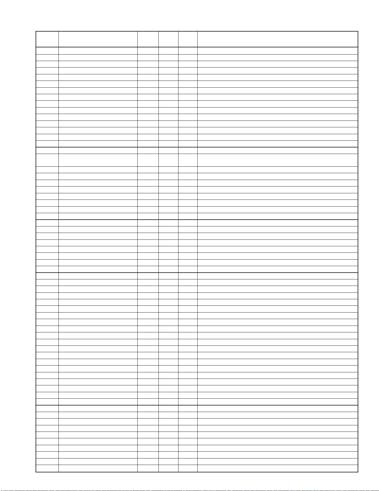
UX-510UA
FO-1470U
SCE114 (IC9) Terminal descriptions
Pin
No. Type Type
64 GPIO[5]/SSCLK2 I/O Hu 13Xs GPIO[5] or SSIF2 clock.
65 GPIO[10]/SSSTAT2 I/O Hu 13Xs GPIO[10] or SSIF2 status.
66 VDRAM −−−DRAM battery power.
67 RASn O − 13Xs (Batt. Pwr.) DRAM row address select.
68 CAS[1]n O − 13Xs (Batt. Pwr.) DRAM column address select.
69 CAS[0]n O − 13Xs (Batt. Pwr.) DRAM column address select.
70 DWRn O − 13Xs (Batt. Pwr.) DRAM write.
71 VBAT −−−Battery power.
72 XIN I Osc1 − (Batt. Pwr.) 32.768kHz Crystal Oscillator input.
73 XOUT O − Osc1 (Batt. Pwr.) 32.768kHz Crystal Oscillator output.
74 WRPROTn O − 1XC (Batt. Pwr.) Write protect during loss of VDD power.
75 CS0n O − 13Xs (Battery Powered) SRAM Chip select.
76 TEST[1] I Hd − (Batt. Pwr.) Test mode.
77 TEST[0] I Hd − (Batt. Pwr.) Test mode.
78 BATRSTn I H − (Batt. Pwr.) Battery power reset input.
79 INTPWRDWNEn I H − (Batt. Pwr.) Internal power down select signal.
80 PWRDWNn I/O H 13Xs (Batt. Pwr.) Indicates a prime power loss from ext./internal source
81 NC I Analog − No Connection.
82 ADGA − VADG − A/D analog ground.
83 VREFn/CLREF I VR- − Negative reference voltage for Video A/D.
84 VIN I VA − Analog Video A/D input.
85 ADGA − VADG − A/D analog ground.
86 ADVA − VADV − A/D analog power.
87 ADXG − VXG − A/D internal ground.
88 VREFp I VR − Positive reference voltage for Video A/D.
89 IVREFn I VR- − Internal negative reference voltage for A/D.
90 IVREFp I VR+ − Internal positive reference voltage for A/D.
91 VDD −−−Digital power.
92 THADI I Analog − Analog Thermal A/D input.
93 OPO[7]/GPO[15] O − 13Xs Keyboard LED strobe 7 or GPO[15].
94 OPO[6]/GPO[14] O − 13Xs Keyboard LED strobe 6 or GPO[14].
95 OPO[5]/GPO[13] O − 13Xs Keyboard LED strobe 5 or GPO[13].
96 OPO[4]/GPO[12]/SSTXD1 O − 13Xs Keyboard LED strobe 4 or GPO[12] or transmit data for SSIF1.
97 OPO[3]/GPO[11] O − 13Xs Keyboard LED strobe 3 or GPO[11].
98 OPO[2]/GPO[10]/RINGER OZ − 13Xs Keyboard LED strobe 2 or GPO[10] or ringer.
99 OPO[1]/GPO[9]/PMPWRCTRL O − 13Xs Keyboard LED strobe 1 or GPO[9] or Printer motor power control.
100 OPO[0]/GPO[8]SMPWRCTRL O − 13Xs Keyboard LED strobe 0 or GPO[8] or Stepper motor power control.
101 OPI[3]/GPIO[24] I/O Hu 13Xs Keyboard return 3 or GPIO[24].
102 OPI[2]/GPIO[23]/SSCLK1 I/O Hu 13Xs Keyboard return 2 or GPIO[23] or SSIF1 clock.
103 OPI[1]/GPIO[22]/SSSTAT1 I/O Hu 13Xs Keyboard return 1 or GPIO[22] or SSIF1 status.
104 OPI[0]/GPIO[21]/SSRXD1 I/O Hu 13Xs Keyboard return 0 or GPIO[21] or SSIF1 receive data.
105 RESETn I/O Hu 2XC Chip reset.
106 VSS −−−Digital ground.
107 GPIO[18]/IRQ[9]n I/O Hu 13Xs GPIO[18] or ext. interrupt priority 9.
108 GPIO[3]/SASCLK I/O Hu 13Xs GPIO[3] or SASIF clock.
109 GPIO[2]/SASRXD I/O Hu 13Xs GPIO[2] or SASIF receive data.
110 GPIO[1]/SASTXD I/O Hu 13Xs GPIO[1] or SASIF transmit data.
111 GPIO[9]/FRDn I/O Hu 13Xs GPIO[9] or flash read enable signal for NAND-type flash memory.
112 GPIO[8]/FWRn I/O Hu 13Xs GPIO[8] or flash write enable signal for NAND-type flash memory.
113 FCSn[2]/VIDCTL[1]/GPO[22] O − 13Xs Flash memory chip select 2 or video control signal 1 or GPO[22].
114 FCSn[1]/VIDCTL[0]/GPO[23] O − 13Xs Flash memory chip select 1 or video control signal 1 or GPO[23].
115 CLK2/GPO[24] O − 13Xs Scanner reset gate control (or clock for CIS scanner) or GPO[24].
116 CLK1n/GPO[25] O − 13Xs Scanner clock-inverted or GPO[25].
117 CLK1 O − 2XC Scanner clock.
118 START O − 2XC Scanner shift gate control.
119 VDD −−−Digital power.
120 TONE O − Analog Analog tone output.
121 VSS −−−Digitai ground.
122 GPIO[25]/STROBEN I/O Hu 13Xs GPIO[25] or P1284 input from host.
123 GPIO[26]/AUTOFDN I/O Hu 13Xs GPIO[26] or P1284 input from host.
124 GPIO[27]/INITN I/O Hu 13Xs GPIO[27] or P1284 input from host.
125 GPIO[28]/SLCTINN I/O Hu 13Xs GPIO[28] or P1284 input from host.
126 GPIO[26]/ACKN O − 13Xs GPIO[26] or P1284 returned status to host.
Pin List I/O
Input Output
Pin Description
(mode dependent).
5 – 4
Page 56

UX-510UA
FO-1470U
SCE114 (IC9) Terminal descriptions
Pin
No. Type Type
127 GPO[27]/BUSY O − 13Xs GPO[27] or P1284 returned status to host.
128 GPO[28]/PERROR O − 13Xs GPO[28] or P1284 returned status to host.
129 GPO[29]/SLCTOUT O − 13Xs GPO[29] or P1284 returned status to host.
130 GPO[30]/FAULTN O − 13Xs GPO[30] or P1284 returned status to host.
131 GPIO[29]/PIOD[0] I/O Hu 13Xs GPO[29] or P1284 data or address driven by asic or host
132 GPIO[30]/PIOD[1] I/O Hu 13Xs GPO[30] or P1284 data or address driven by asic or host
133 GPIO[31]/PIOD[2] I/O Hu 13Xs GPO[31] or P1284 data or address driven by asic or host
134 GPIO[32]/PIOD[3] I/O Hu 13Xs GPO[32] or P1284 data or address driven by asic or host
135 GPIO[33]/PIOD[4] I/O Hu 13Xs GPO[33] or P1284 data or address driven by asic or host
136 GPIO[34]/PIOD[5] I/O Hu 13Xs GPO[34] or P1284 data or address driven by asic or host
137 GPIO[35]/PIOD[6] I/O Hu 13Xs GPO[35] or P1284 data or address driven by asic or host
138 GPIO[36]/PIOD[7] I/O Hu 13Xs GPO[36] or P1284 data or address driven by asic or host
139 VDD −−−Digitai power.
140 GPIO[0]/SR4IN I/O Hu 13Xs GPIO[0] or from secondary EXTIA SOUT to DSP.
141 GPO[31]/SR3OUT O − 13Xs GPO[31] or a signal to the secondary ext. IA (SIN pin) from the DSP.
142 GPIO[37]/IRQ15n I/O Hu 13Xs GPIO[37] or a signal from the ext. IA to a DSP status register.
143 IARESET O − 13Xs A reset from the DSP to the ext. IA (POR pin).
144 IACLK/DSPCSn O − 13Xs A signal from the DSP to the ext. IA (MCLK pin) or ext. modem chip
145 IA1CLK I/O H 13Xs A signal from the ext. IA (ICLK pin) to the DSP.
146 SR3IN/DSPIRGn I H 13Xs A signal from the primary ext. IA (SOUT pin) to the DSP or ext.
147 SR4OUT O − 13Xs A signal to the primary ext. IA (SIN pin) from the DSP.
148 SR1IO I/O H 13Xs A signal to the ext. IA (CTRL1 pin) from the DSP.
149 SA1CLK I/O H 13Xs A signal from the ext. IA (FSYNC pin) to the DSP.
150 VSSPLL −−−Ground for PLL.
151 TSTCLK O − 13Xs Test clock, used to synchronize ext. logic.
152 DEBUGn I Hu − External non-maskable input (NMI).
153 RDn O − 13Xs Read strobe.
154 WRn O − 13Xs Write strobe.
155 SYNC/GPO[20] I/O Hu 13Xs Indicates a CPU op code fetch cycle or GPO[20].
156 ROMCSn O − 13Xs ROM chip select.
157 CS1n/GPO[21] O − 13Xs I/O chip select or GPO[21].
158 VSS −−−Digital ground.
159 SXIN I OSC0 − 32.256MHz crystal oscillator input.
160 SXOUT O − OSC0 32.256MHz crystal oscillator output.
161 VDD −−−Digital power.
162 PM[3]/GPO[3] O − 13Xs Programmable print motor control pin or GPO[3].
163 PM[2]/GPO[2] O − 13Xs Programmable print motor control pin or GPO[2].
164 PM[1]/GPO[1] O − 13Xs Programmable print motor control pin or GPO[1].
165 PM[0]/GPO[0] O − 13Xs Programmable print motor control pin or GPO[0].
166 SM[3]/GPO[7] O − 13Xs Programmable scan motor control pin or GPO[7].
167 SM[2]/GPO[6] O − 13Xs Programmable scan motor control pin or GPO[6].
168 SM[1]/GPO[5] O − 13Xs Programmable scan motor control pin or GPO[5].
169 SM[0]/GPO[4] O − 13Xs Programmable scan motor control pin or GPO[4].
170 REGDMA/GPO[18]/CLKConfig[0] O − 13Xs Register select cycle/dma cycle or GPO[18] and sxin clock divider
171 WAITn/GPO[19]/CLKConfig[1] I/O Hu 13Xs Wait state/halt state indication or GPO[19] and sxin loc k divider config.
172 VDDPLL −−−Power for PLL.
173 D[7] I/O Tu 13Xs CPU data bus.
174 D[6] I/O Tu 13Xs CPU data bus.
175 D[5] I/O Tu 13Xs CPU data bus.
176 D[4] I/O Tu 13Xs CPU data bus.
Pin List I/O
Input Output
Pin Description
(mode dependent).
(mode dependent).
(mode dependent).
(mode dependent).
(mode dependent).
(mode dependent).
(mode dependent).
(mode dependent).
select.
modem interrupt input.
config. during reset.
during reset.
5 – 5
Page 57
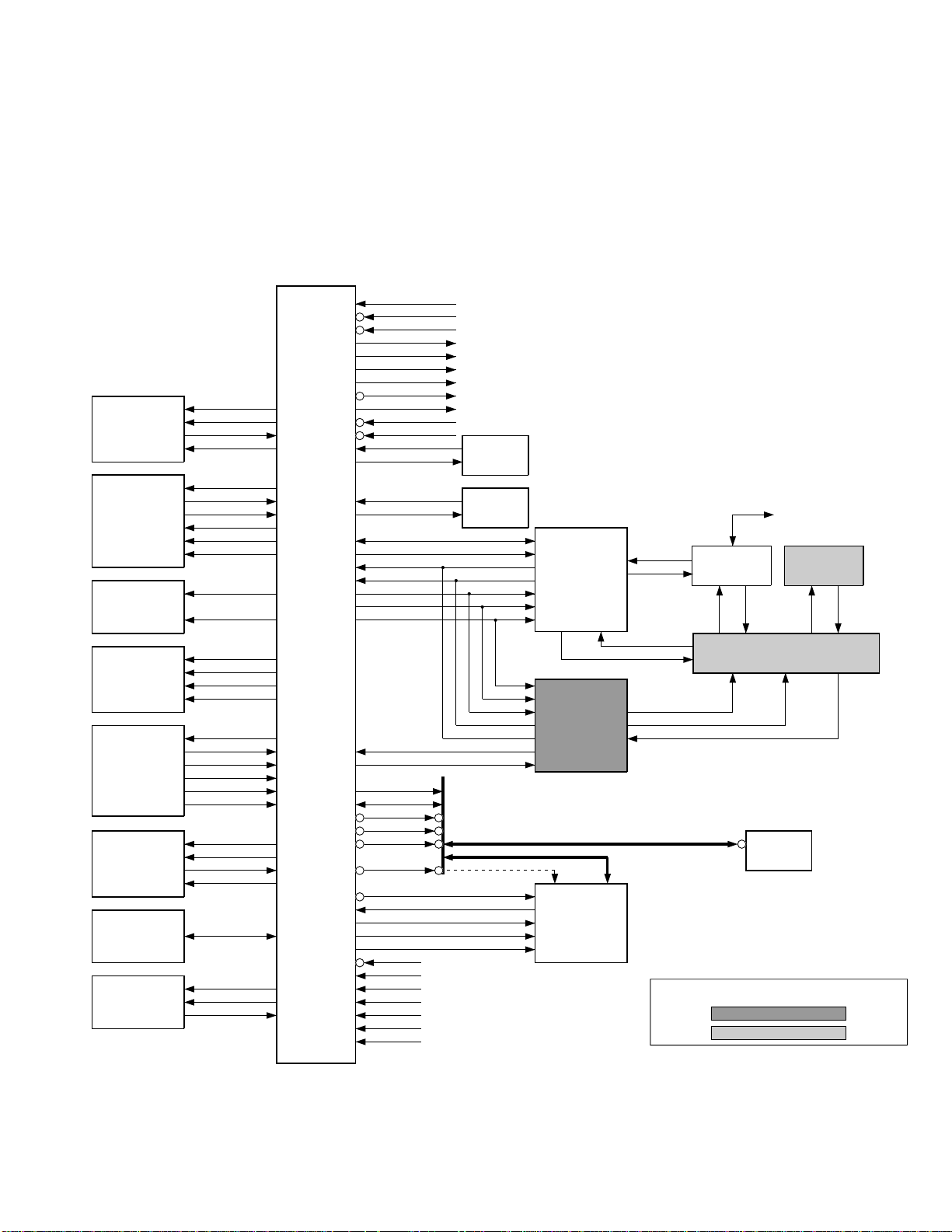
(2) Panel control block
The following controls are performed by the SCE114.
• Operation panel key scanning
• Operation panel LCD display
(3) Mechanism/recording control block
• Recording control block diagram (1)
OPERATOR
PANEL,
KEYPAD,
LEDS & LCD
PRINTER DATA
CONTROI &
SENSORS
PRINTER &
SCANNER
MOTOR DRIVERS
SCANNER
CONTROLS &
SENSORS
SCANNER
VIDEO
PREPROCESSING
SERIAL SYNC
PORTS
(2)
(SSIF)
PURPOSE I/O
SYNC/ASYNC
SERIAL PORT
SASIF
OPO[7:0]*
OPI[3:0]*
LEDCTL*
LCDCS*
STRB[3:0]
STRBPOL
THADI
PDAT
PCLK
PLAT
PM[3:0]*
SM[3:0]*
START
CLK2
CLK1
CLK1N
VIDCTL[1:0]
VIN
VREFP
VREFN
IVREFP
IVREFN
SSCLK[2:1]*
SSTXD[2:1]*
SSRXD[2:1]*
SSSTAT[2:1]*
GPIOGENERAL
SASCLK*
SASTXD*
SASRXD*
SCE114
1-CHIP
FAX ENGINE
TEST[1:0]
BATRSTN
RESETN
TONE
ALTTONE
TSTCLK
REGDMA
WAITN
SYNC
PWRDWNN
INTPWRDWNEN
XIN
XOUT
SXIN
SXOUT
SR3IN
SR4OUT
IA1CLK
SA1CLK
IACLK
SR1IO
IARESET
SR4IN*
SR3OUT*
A[23:0]
D[7:0]
RDN
WRN
ROMCSN
CS[5:0]N*
WRPROTN
FRDN*
FRWN*
FCLE*
FCSN[2:0]
DEBUGN
VDD
VDRAM
VBAT
VSS
ADVA
ADGA
RTC
CRYSTAL
SYSCLK
CRYSTAL
EXTERNAL BUS
IA
SECONDARY
IA
CAS[0,1]N, RASN, DWRN
CS3N,
CS4N**
FLASH MEMORY
D7[7:0]
TELEPHONE
LINE
RXIN
TXOUT
RIN
TXOUT
SPKRH
SPKRL
RIN
NOTES: * ALTERNATIVE GPO, GPI OR GPIO LINES
**FOR SAMSUNG NAND-TYPE FLASH
LINE
INTERFACE
RXA
TXA
SPEAKERPHONE ONLY
VOICE OR SPEAKERPHONE
ANALOG
SWITCH
DRAM
(OPTION)
SPEAKER
MICROPHONE
CIRCUIT
SPKR
UX-510UA
FO-1470U
MIC
Fig. 4
5 – 6
Page 58
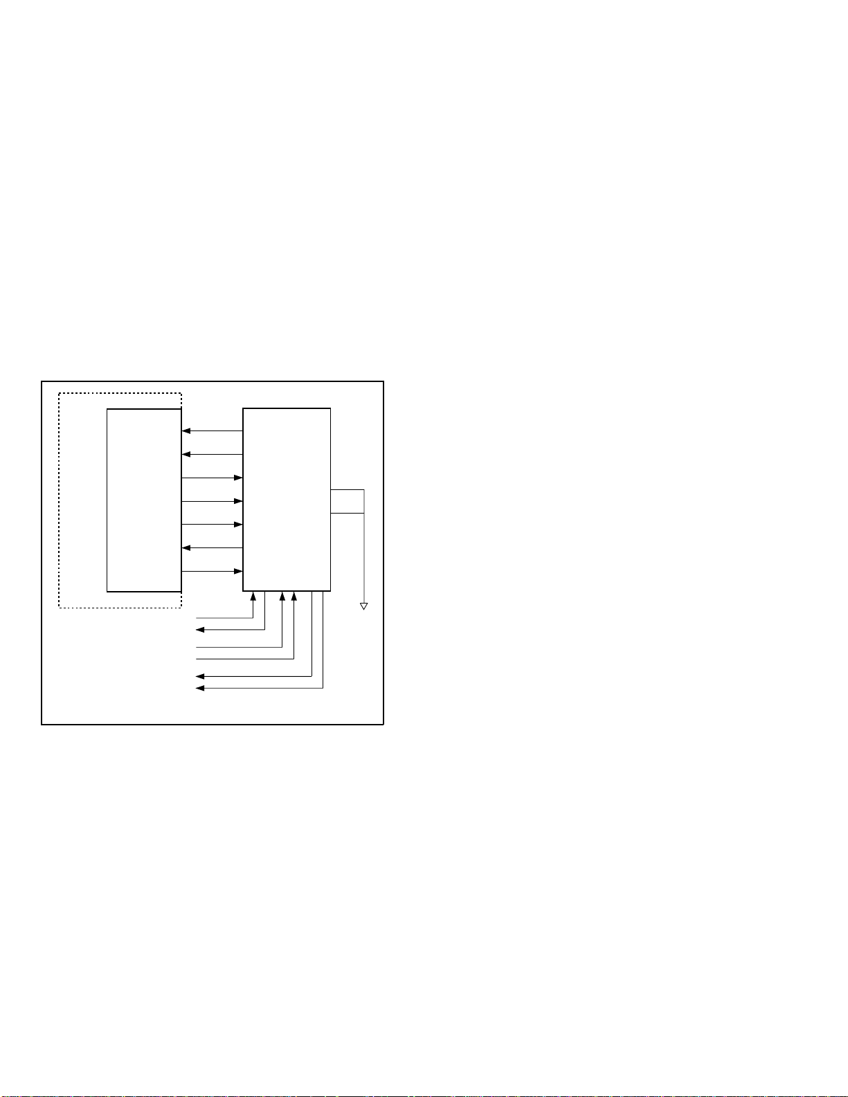
UX-510UA
FO-1470U
(4) Modem (SCE114/20415) block
INTRODUCTION
The CONEXANT SCE114 modem is a synchronous 14400 bits per second (bps) half-duplex modem with error detection and DTMF reception.
It has low power consumption and requires +5V and +3.3V DC power
supply.
The modem can operate over the public switched telephone network
(PSTN) through line terminations provided by a data access arrangement (DAA).
The SCE114 is designed for use in Group 3 facsimile machines.
The modem satisfies the requirements specified in ITU-T recommendations V.17, V.29, V.27 ter, V.21 Channel 2 and T.4, and meets the binary
signaling requirements of T.30.
The modem can operate at 14400, 12000, 9600, 7200, 4800, 2400, or
300 bps, and also includes the V.27 ter short training sequence option.
The modem can also perform HDLC framing according to T.30 at 9600,
7200, 4800, 2400, or 300 bps.
The modem features a programmable DTMF receiver and three programmable tone detectors which operate concurrently with the V.21
channel 2 receiver.
The voice mode allows the host computer to efficiently transmit and
receive audio signals and messages.
DSP IA
SA1CLK
IA1CLK
SR4OUT
SCE114
TYPICAL EXTERNAL HYBRID
TYPICAL MICROPHONE
CIRCUIT
TYPICAL SPEAKER CIRCUIT
IACLK
SR1IO
SR3IN
GPO0
LINEIN
LINEO
MICIN+
MICIN–
SPKRO+
SPKRO–
Fig. 5
FSYNC
ICLK
MCLK
CTRLSIN
SIN
SOUT
POR
Connections for MODE 0
and MODE 1 pins are
shown for a Line IA.
MODE 0
MODE1
GND
FEA TURES
• Group 3 facsimile transmission/reception
- ITU-T V.17, V.33, V .29, V.27 ter, T.30, V .21 Channel 2, T.4
- ITU-T V.17 and V.27 ter short train
- HDLC framing at all speeds
- Receive dynamic range: 0 dBm to -43 dBm
- Automatic adaptive equalization
- Fixed and programmable digital compromise equalization
- DTMF detect and tone detect
- ITU-T V.21 Channel 2 FSK 7E Flag Detect
- Ring detector
- Programmable transmits level
- Programmable single/dual tone transmission
• V.23 and Type I Caller ID
- Full-duplex modes:
TX = 75 bps. RX = 1200 bps
TX = 1200 bps. RX = 75 bps
- Half-duplex mode:
TX = RX = 1200 bps
- Serial and parallel data modes
- Programmable parallel data mode
- 5, 6, 7 or 8 data bits
- 1 or 2 Stop bits
- Mark, Space, Even, or Odd Parity
- Break function
- Transmitter squelch
- Compromise equalizer
• Programmable interface memory interrupt
• Eight General Purpose Input (GPI) and eight General Purpose Out-
put (GPO) pins for host assignment
• DTE interface: two alternate ports
- Selectable microprocessor bus (6500 or 8085)
- ITU-T V.24 (EIA/TIA-232-E compatible) interface
• TTL and CMOS compatible
• 3.3V/5V operation
• Power consumption
- Operating Mode: 200 mW (Basic), 275 mW (-V option). 300 mW
(-VS option)
- Sleep Mode: 1 ma (Basic. -V option and -VS option)
5 – 7
Page 59
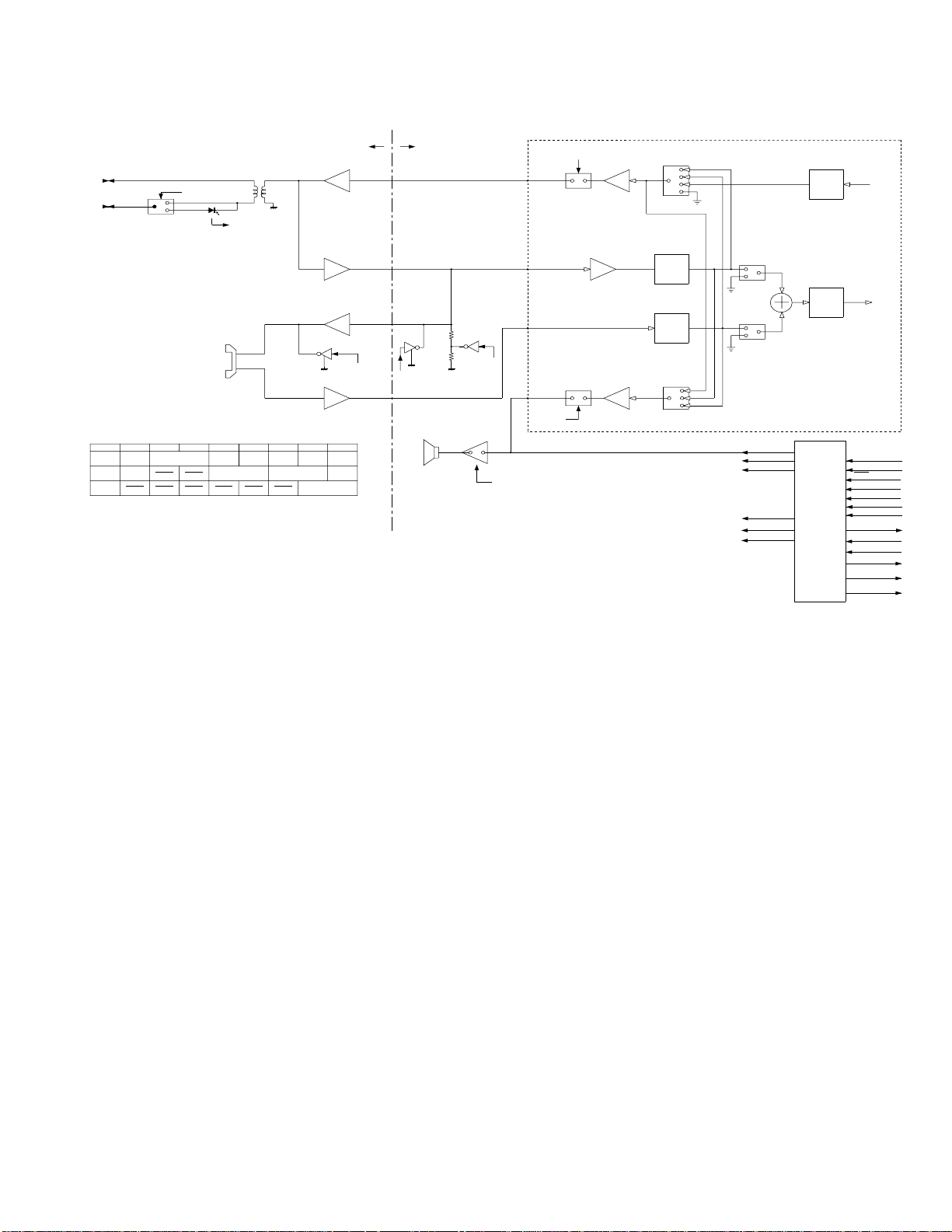
[3] Circuit description of TEL/LIU PWB
(1) TEL/LIU block operational description
1) Block diagram
MICBIAS
LINE SEL
TELMUTE
SEL
TXOUT
RXIN
TELIN
DTMFMUTE
TELOUT
SPEAKER
L1
L2
IACR1
IACR2
IACR3
CML
M
C
B
BIT7 BIT6 BIT5 BIT4 BIT3 BIT2 BIT1 BIT0
DAC
MIC GAIN L/O E
GAIN
TXRX
LOOP
CI
HANDSET
RX
TX
SPKR E
LINEOUT
ATTENUATION
ADC
GAIN
RXTXLOOP
L/I E MIC E
UX-510UA
FO-1470U
INTEGRATED ANALOG
SPKRP-P
MICP
LINEIN
LINEOUT
LINEOUT
ENABLE
SP OUT
ENABLE
SP
DRIVER
MIC
GAIN
0,20,25,30dB
LINE
DRIVER
MUTE,0,
–6,–12dB
CONTROL PWBTEL/LIU PWB
RCV VOL
SPMUTE
RTLOOP
MIC IN
LPF
LINE IN
LPF
LNINSEL
20415
(0:1)
(1:0)
(0:0)
(1:1)
MIC ENABLE
1
0
1
0
(0:0)
(1:1)
(1:0)
MIC
ENABLE
LINE IN
ENABLE
BZOUT
CML
SPMUTE
DTMFMUTE
RCVOL
VTHON
DAC
DAC GAIN
0,6dB
ADC
ADC GAIN
0,–4dB
FAX
ENGINE
SCE114
HS
CI
CSWI
PESNS
FRSNS
ORGSNS
PSNS
LEDON
RHS
DRSNS
TXMUTE
TELMUTE
IA-RESET
SIN
SOUT
2) Circuit description
The TEL/LIU PWB is composed of the following 7 blocks.
1. Speech circuit section
2. Dial transmission section
3. Speaker amplifier section
4. Ringer circuit section
5. Externally connected TEL OFF HOOK detection circuit
6. CI detection circuit
7. Signal/DTMF transmission level & receiving level
Fig. 6
3) Block description
1. Speech circuit section
• The receiver volume is an electronic volume type, this model is
switched in 3 steps.
2. Dial transmission section
• D .P. transmission: The CML rela y is turned on and off f or control in
the DP calling system. (Refer to the attached sheet.)
• DTM transmission: It is formed in the modem, and is output.
3. Speaker amplifier section
• Ringer volume :It is controlled by the combination of the
attenuator value of the LINE DRIVER in the
modem and the ringer sending level sent from
the modem.
• Speaker volume :It is controlled by the attenuator value of the
LINE DRIVER in the modem.
4. Ringer circuit section
• The ringer sound is formed in the tone of modem when CI signal is
detected. The amplifier circuit drives the speak er of the main body.
5 – 8
Page 60
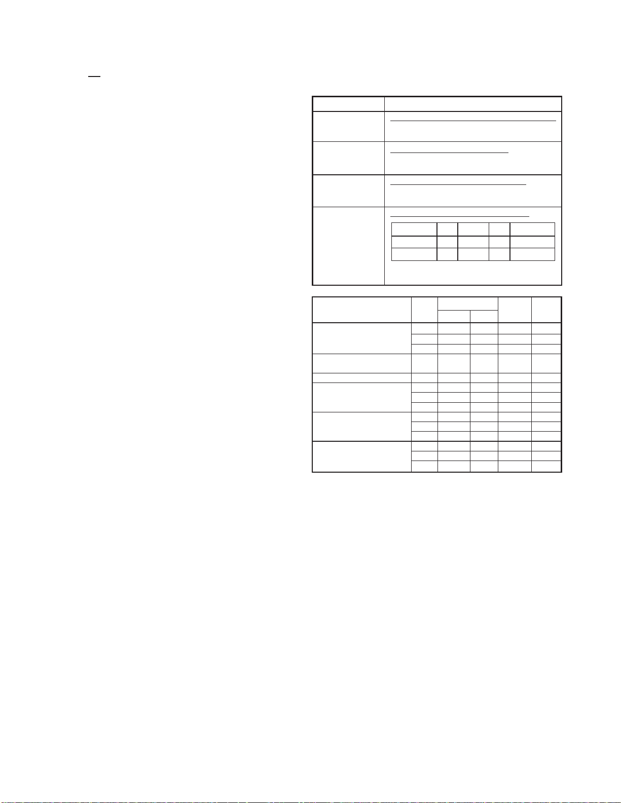
UX-510UA
FO-1470U
5. Externally connected TEL OFF HOOK detection circuit section
• The circuit current detection is turned on together with OFF HOOK
of main body or OFF HOOK of externally connected TEL. ON of
CML OFF (HS=L) is judged as OFF HOOK of externally connected
TEL.
6. CI detection circuit
• CI is detected by the photo coupler which is integrated in series in
the primary side TEL circuit well proven in the existing unit.
7. Signal/DTMF transmission level & receiving level
•
Signal transmission level setting: A TT -10 dB Circuit output: -12 dBm.
• DTMF transmission level setting: HF -3.5 dBm LF -5.0 dBm
Thus, set the level.
4) Signal selection
The following signals are used to control the transmission line of TEL/
FAX signal. For details, refer to the signal selector matrix table.
[Control signals from output port]
Signal Name Description
CML Line connecting relay and DP generating relay
(The circuit is located H: Line make
in the TEL/LIU PWB.) L: Line break
SP MUTE Speaker tone mute control signal
(The circuit is located H: Muting (Power down mode)
in the TEL/LIU PWB.) L: Muting cancel (Normal operation)
TEL MUTE H: Muting
RCVOL
DTMFMUTE
(The circuit is located
in the control PWB.)
Handset reception mute control signal
L: Muting cancel
Handset receiver volume control signal
Volume High Middle Low
RCVOL
DTMFMUTE L L H H
Note: The DTMF sending listed above is DTMF signal
sending in the handset OFF-HOOK mode.
LHL L
DTMF sending
VOLUME SETTING
Receiver volume setting Low 0 1
High 0 0
Middle 1 0
DTMF T ransmission Fixed 0 1
volume setting (Receiver)
Key buzzer volume setting Fixed
Speaker volume setting Low 1 1
Middle 1 0
High 0 1
Ringer volume setting Low 1 1
Middle 1 0
High 0 1
DTMF speaker volume Low 1 1
setting Middle 1 0
High 0 1
LINEOUT A RCVOL DTME
(HIGH) (LOW) MUTE
5 – 9
Page 61
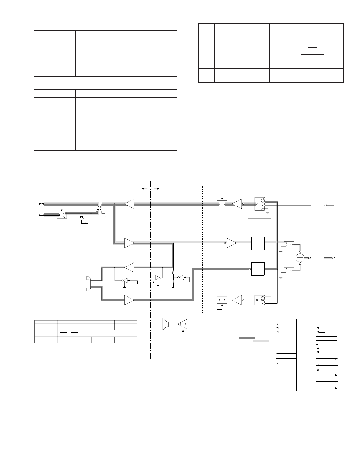
[Signals for status recognition according to input signals]
Signal Name Function
RHS
H:The handset is in the on-hook state.
L: The handset is in the off-hook state.
CI Incoming call (CI) detection signal
DRSNS
H: Door open.
L: Door close.
[Other signals]
Signal Name Function
TEL IN Receiving signal from line or modem
TEL OUT Transfer signal to line
SPOUT Speaker output signal
TXOUT
RXIN
Transmission (DTMF) analog signal output
from modem
Reception (DTMF, others) analog signal
into modem
(Example: TEL speaking)
L1
L2
CML
M
C
B
CI
TXOUT
CONTROL PWBTEL/LIU PWB
input
No. Signal Name (CNLIUA)
1 PE1
2 TEL OUT
3 TEL IN
4 TEL MUTE
5
CI
6HS
7 CML
INTEGRATED ANALOG
20415
SP OUT
SPKRP-P
ENABLE
SP
DRIVER
RTLOOP
UX-510UA
FO-1470U
No. Signal Name (CNLIUA)
8 TXOUT
9 RXIN
10 RHS
11 DOOR SW
(0:1)
(1:0)
(0:0)
(1:1)
12
13
14
MIC ENABLE
+5V
DG
+24V
DAC GAIN
0,6dB
DAC
SIN
HANDSET
RX
TX
BIT7 BIT6 BIT5 BIT4 BIT3 BIT2 BIT1 BIT0
IACR1
IACR2
IACR3
DAC
GAIN
TXRX
LOOP
MIC GAIN L/O E
SPKR E
LINEOUT
ATTENUATION
ADC
GAIN
RXTXLOOP
L/I E MIC E
MICBIAS
SEL
LINE SEL
RXIN
TELIN
TELMUTE
TELOUT
DTMFMUTE
SPEAKER
RCV VOL
SPMUTE
Fig. 7
MICP
0,20,25,30dB
LINEIN
LINEOUT
LINEOUT
ENABLE
TEL SPEAKING:
FAX SENDING/RECEIVING:
MIC
GAIN
LINE
DRIVER
MUTE,0,
–6,–12dB
MIC IN
LPF
LINE IN
LPF
LNINSEL
MIC
ENABLE
1
0
LINE IN
ENABLE
1
0
(0:0)
(1:1)
(1:0)
BZOUT
CML
SPMUTE
DTMFMUTE
RCVOL
VTHON
FAX
ENGINE
SCE114
ADC
ADC GAIN
0,–4dB
HS
CI
CSWI
PESNS
FRSNS
ORGSNS
PSNS
LEDON
RHS
DRSNS
TXMUTE
TELMUTE
IA-RESET
SOUT
5 – 10
Page 62
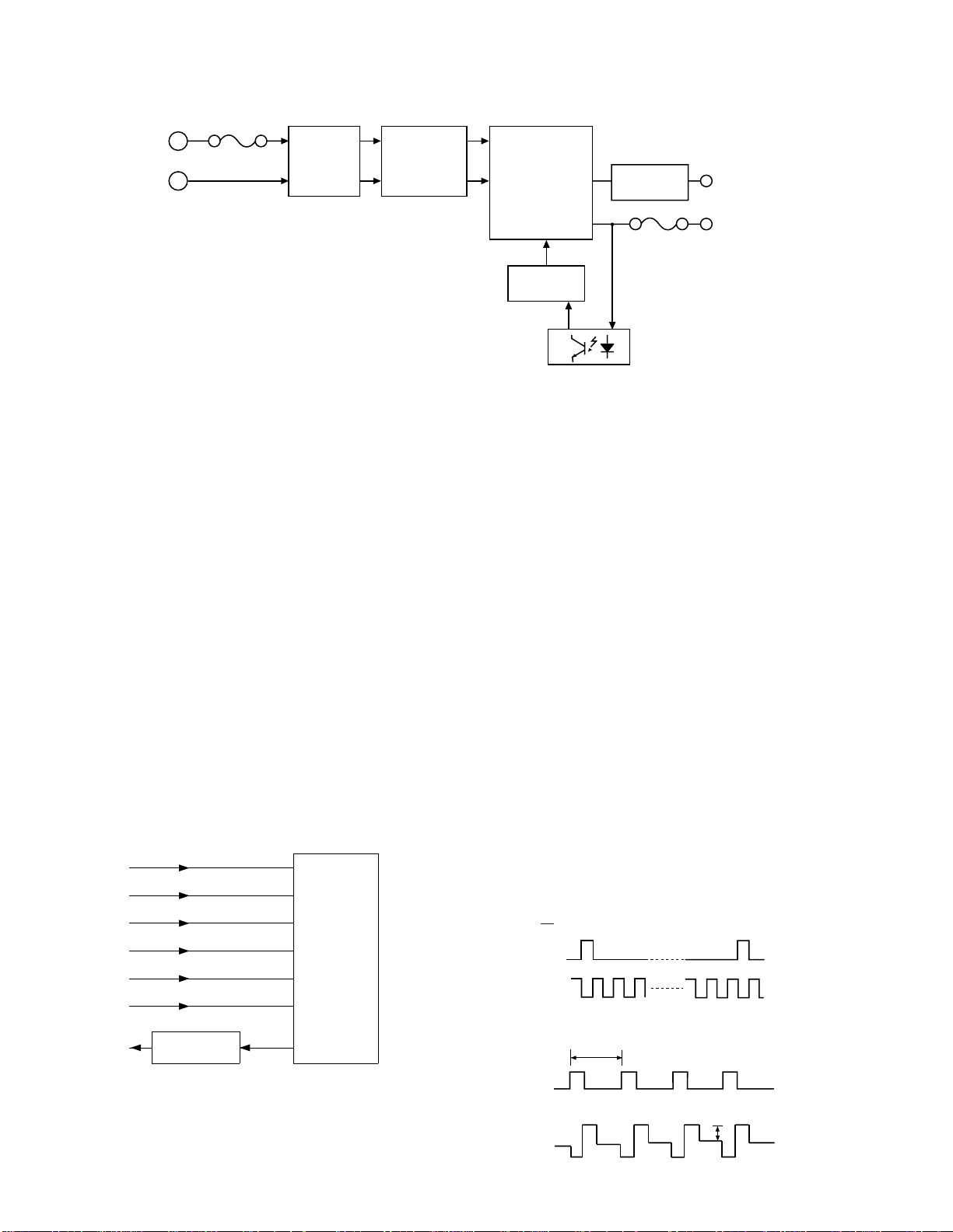
UX-510UA
FO-1470U
[4] Circuit description of power supply PWB
1. Block diagram
2.5A/125V
AC IN
Noise
Filter
Circuit
Rectifying
Smoothing
Circuit
Fig. 8
Switching
Circuit
(RCC system)
Control
Circuit
Photo Coupler
Regulator
Circuit
FUSE
4A/72V
+5V
+24V
2-1. Noise filter circuit
The input noise filter section is composed of L1 and C1, C15, which
reduces normal mode noise from the AC line and common mode noise
to the AC line.
2-2. Rectifying/smoothing circuit
The AC input voltage is rectified by diode stack DS1 and smoothed by
capacitor C2 to supply DC voltage to the switching circuit section.
2-3. Switching circuit
This circuit includes MOS FET Q1 and the gate drive circuit, and components around Q1.
In this circuit, the DC voltage supplied from the rectifying/smoothing
section is converted into high frequency pulses by ON/OFF repetition of
Q1.
[5] Circuit description of CCD PWB
The CCD board picks up optical information from the document, converts it into an electrical (analog) signal and transfers it to the control
board.
(1) Block diagram
T
Φ
1
Φ
2
Φ
R
Φ
+5V
GND
CCD
TCD1208AP
2-4. Control circuit
This circuit controls output voltage of +24V by adjusting ON period of
Q1, looking at signal from photo coupler PC1.
In this operation IC1 takes charge of important part.
The over current protection is performed by br inging Q1 to OFF state
through detection of voltage of T1 subwiding.
The over voltage protection is performed by operating the over current
protection circuit through detection of zener diode ZD4 and short-circuiting
of load.
2-5. +5V circuit
DC voltage supplied by rectifying the output of transf ormer T1 with diode
D8 is stabilized by 3-terminal regulator IC1.
(2) Description of blocks
1. CCD
The TCD1208AP is a highly sensitive charged coupled image sensor
that consists of 2160 picture elements.
Receiving four drive signal (øT, ø2, ø1, øR) from the control board, the
transferred photoelectric analog signal OS is impedance converted, and
the signal VO, is supplied to the control board.
2. W aveforms
1. ø1, ø2 (=ø1) signals within the control board.
øT
ø1 (=ø2)
Approx. 5V
0V
Approx. 5V
0V
VO
OUTPUT CIRCUIT
(emitter follower)
Fig. 9
OS
5 – 11
2. OS ø
OS
1.74µ SEC
Approx. 5V
øR
Approx. 100mV
0V
Fig. 10
Page 63
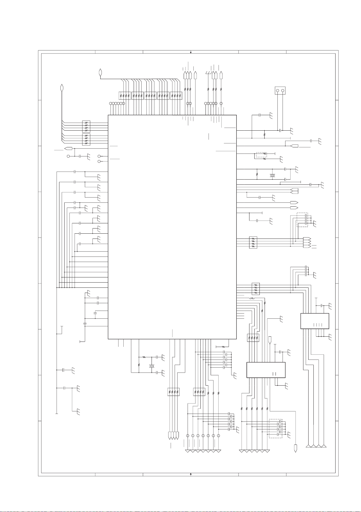
A
A
B
B
C
C
D
D
E
E
F
F
G
G
H
H
I
I
6 6
5 5
4 4
3 3
2 2
1 1
LV125AIC3
1Y4111Y381Y261Y1
3
1A4121A391A251A1
2
VCC
14
2OE41OE
1
GND
7
3OE104OE
13
<G>
R1270
R1230
R140
10K
<K>
<L>
<M>
C137
1
C114
2.2
DG
<BATRST>
C117 1
C142
1
C140
1
RA 5
470
HCT244IC2
2Y432Y352Y2
7
2Y191Y4121Y3141Y2161Y1
18
2A4172A3152A2132A1
11
1A481A361A241A1
2
VCC
20
2OE191OE
1
GND
10
C133
C131
C112
C132
C113
C135
0.1
C110
C109
1000P X 7
C6
220/6.3
+
<A>
<H>
< I >
C118
1
<J>
RA14
470
R129
220K
C164
100P X7
C163
C146
2.2
R171
1M
R170
220
R141270
R143270
R142270
C147
2.2
IC9
SCE114(1/2)
TEST077TEST1
76
D0
5
D1
4
D2
3
D3
2
D4
176
D5
175
D6
174
D7
173
A236A227A218A209A1910A1811A1713A1614A1515A1416A1318A1219A1120A10
21A922A823A724A625A526A427A032A329A230A131RD153WR154
ROMCS
156
CS1
157
CS0
75
1
2
3
45
6
7
8
1
2
3
45
6
7
8
1
2
3
45
6
7
8
1
2
3
45
6
7
8
1
2
3
45
6
7
8
SYNC
155
REGDMA/CLKCONFIG0
170
WAIT/CLKCONFIG1
171
RAS
67
CAS069CAS1
68
DWR
70
WRPROT
74
BATREST
78
VBAT
71
PWRDWN
80
INTPWRDOWNE
79
XOUT
73
XIN
72
+VREF
88
-VREF/CLREF
83
VIN
84
THADI
92
TONE
120
ALTTONE/GPIO20
33
OPI0
104
OPI1
103
OPI2
102
OPI3
101
SM0
169
SM1
168
SM2
167
SM3
166
VDRAM
66
LEDCTL
59
OPO0
100
OPO1
99
OPO2
98
OPO3
97
OPO4
96
OPO5
95
OPO6
94
OPO7
93
SXIN
159
SXOUT
160
CLK1
117
CLK2
115
CLK1N/GPO25
116
START
118
STRB048STRB147STRB246STRB345PDAT43PCLK42PLAT44STRBPOL
49
VSS
17
VSS
41
VSS
58
VSS
106
VSS
121
VSS
158
VSS
150
VSS
1
TETCLK
151
RESET
105
DEBUGN
152
VDDPLL
172
VDD
161
VDD
139
VDD
119
VDD
91
VDD
50
VDD
28
VDD
12
IVREFP
90
IVREFN
89
ADXG
87
ADGA
82,85
ADVA
86
LCDCS
61
C120
N.M.
RA 6
470
C136
1
C130
1
C134
2.2
C139
1
R125
10K
C145
C123
C124
C122
C121
C128
1
C127
1
RA 7
270
RA 8
270
R131
10K
R114
N.M.
C148
1000P
C141
2.2
C161
2.2
C173
C172
C156
C155
N.M.
R133 270
C179
R136 270
R134 270
C178
C177
R130
270
C144
C152
R128
270
L107
0
RA 10
270
RA 9
270
C160
2.2
C175
15P
C174
15P
32.256MHz
X2
R1160
R1170
R1650
R1880
R1890
C159
2.2
R1980
C151
1000P
C150
1000P
C149
1000P
C143
1000P
R113
10M
32.768kHz
X1
C158
2.2
C116
33P
RA 11
1K
C157
2.2
C115
18P
R1240
<B>
<D>
<E>
<C>
<F>
RA 3
270
RA 2
270
RA 4
270
C138
1
RA1
470
+3.3V
+3.3V
+3.3V
+5V
+3.3V
+3.3V
VBAT
+3.3V
+3.3V
+3.3V
RD
WR
BZOUT1
D[7:0]
CNPN-12
CNPN-14
CNPN-11
CNPN-15
ROMCS
DWR
CAS0
RAS
VIN
BZOUT2
A[18:0]
PWRDWN
TPB
TPA
TPA
TPB
CNPN-10
CNPN-13
CNPN-2
CNPN-3
CNPN-4
CE1
START
CLK1
CLK2
CLK1
CNPN-1
CNTH-13
CNTH-14
CNTH-3
CNTH-12
CNTH-4
CNTH-11
CNTH-15
VIDCNT1-A
THADI
VIDCNT1
DG
DG
D0
D1
D2
D3
D4
D5
D7
DGA
DGA
DGA
(5-5F)
(2-4G)
(2-5A)
(4-1B)
RESET0
SEN3
SEN2
SEN1
E
SEN4
SEN0
DG
DG
DG
DG
DGA
D6
A0
A3
A13
A11
A15
(2-6A)
A8
A7
A18A9A16
A14
A17
A5
A4
A10
A12
A1A6A2
DG
DG
DG
DG
DGA DGADGA
DGA
DGA DGADGA
DG
DGA DGA
DGA
KEN4A
KEN1A
KEN3A
KEN2A
DG
DG
(5-5F)
(5-4F)
(5-4F)
(6-3I)
(6-3F)
(2-4G)
DGA
(2-3G)
(2-4D,1E)
(2-4A)
(2-4D)
(6-3I)
(4-2D)
(2-4G)
(5-3A)
(5-2A)
(5-2A)
DGA
DG
DATA
STRB3
LATCH
PCLK
STRB1
STRB4
STRB2
DG
DG
(3-1A)
(5-4B)
(6-3F)
(5-2A)
DG
DG
4
3
2
18
7
6
5
4
3
2
18
7
6
5
1
2
3
45
6
7
8
1
2
3
45
6
7
8
1
2
3
45
6
7
8
1
2
3
45
6
7
8
1
2
3
45
6
7
8
CHAPTER 6. CIRCUIT SCHEMATICS AND PARTS LAYOUT
UX-510UA
FO-1470U
[1] Control PWB circuit Main control block 1/6
6 – 1
Page 64
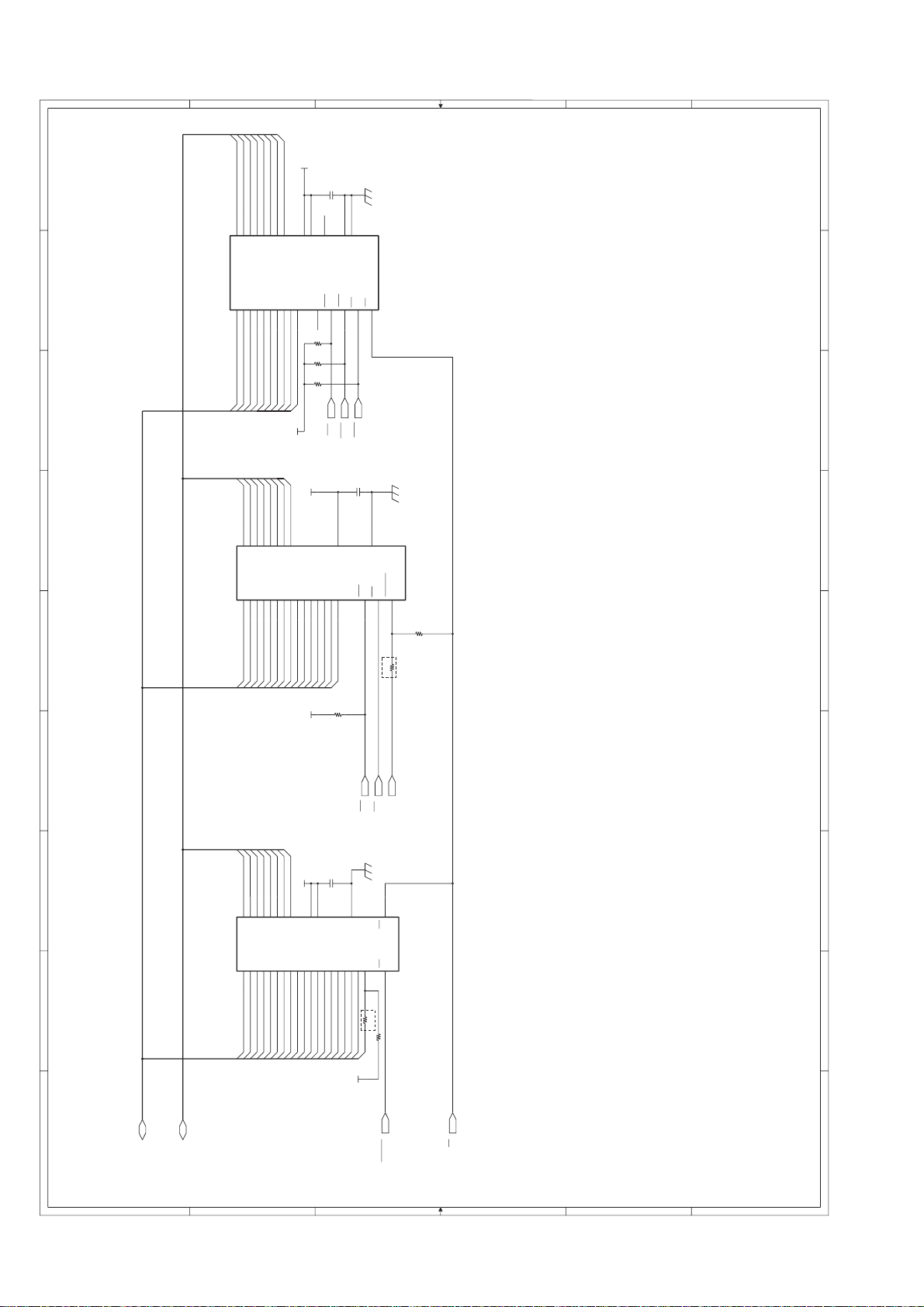
UX-510UA
A
A
B
B
C
C
D
D
E
E
F
F
G
G
H
H
I
I
6 6
5 5
4 4
3 3
2 2
1 1
R221
10K
R222
10K
C129
0.1
R220
10K
IC 4
27L020
A012A111A210A39A48A57A66A75A827A926A1023A1125A124A1328A1429A153A162A1730CE
22
OE
24
A18
31
VPP
1
D013D114D215D317D418D519D620D7
21
VCC
32
GND
16
IC 8
W24258
A0
10
A1
9A28A37
A46A55A6
4
A73A825A924A1021A1123A122A1326A141CS120CS2/OE
22
WE
27
IO111IO212IO313IO415IO516IO617IO718IO8
19
VCC
28
VSS
14
IC 5
MSM51V4800E
VCC
1
WE
7
RAS
8
A9
9
VCC
14
GND
15
OE
22
CAS
23
GND
28
DQ02DQ13DQ24DQ35DQ424DQ525DQ626DQ7
27
A010A111A212A313A416A5
17
A618A719A820NC
6
NC
21
R105
N.M.
R104
10K
C100
0.1
R118
N.M.
R119
0
C126
0.1
R115
22K
+3.3V
+3.3V
VBT
VBT
+3.3V
+3.3V
CAS0
RAS
WR
CE1
ROMCS
RD
A[18:0]
D[7:0]
CE2
DWR
A0A1A2A3A4A5A6A7A8A9A10
A11
A12
A13
A14
A15
A16
A17
A18
D0D1D2D3D4D6D7
D5
A0A1A3A2A4A5A7A6A8
A9
D0D1D2D3D4D5D6
D7
DG
DG
(1-5I)
(1-6I)
(1-3I)
(1-3I)
(1-3I)
(1-4D)
D0D1D2D3D4D6D7
D5
A0A1A2A3A4A5A6A7A8A9A10
A11
A12
A13
A14
(1-3I)
(1-3I)
(1-3I)
(1-3I)
DG
FO-1470U
Memory block 2/6
6 – 2
Page 65
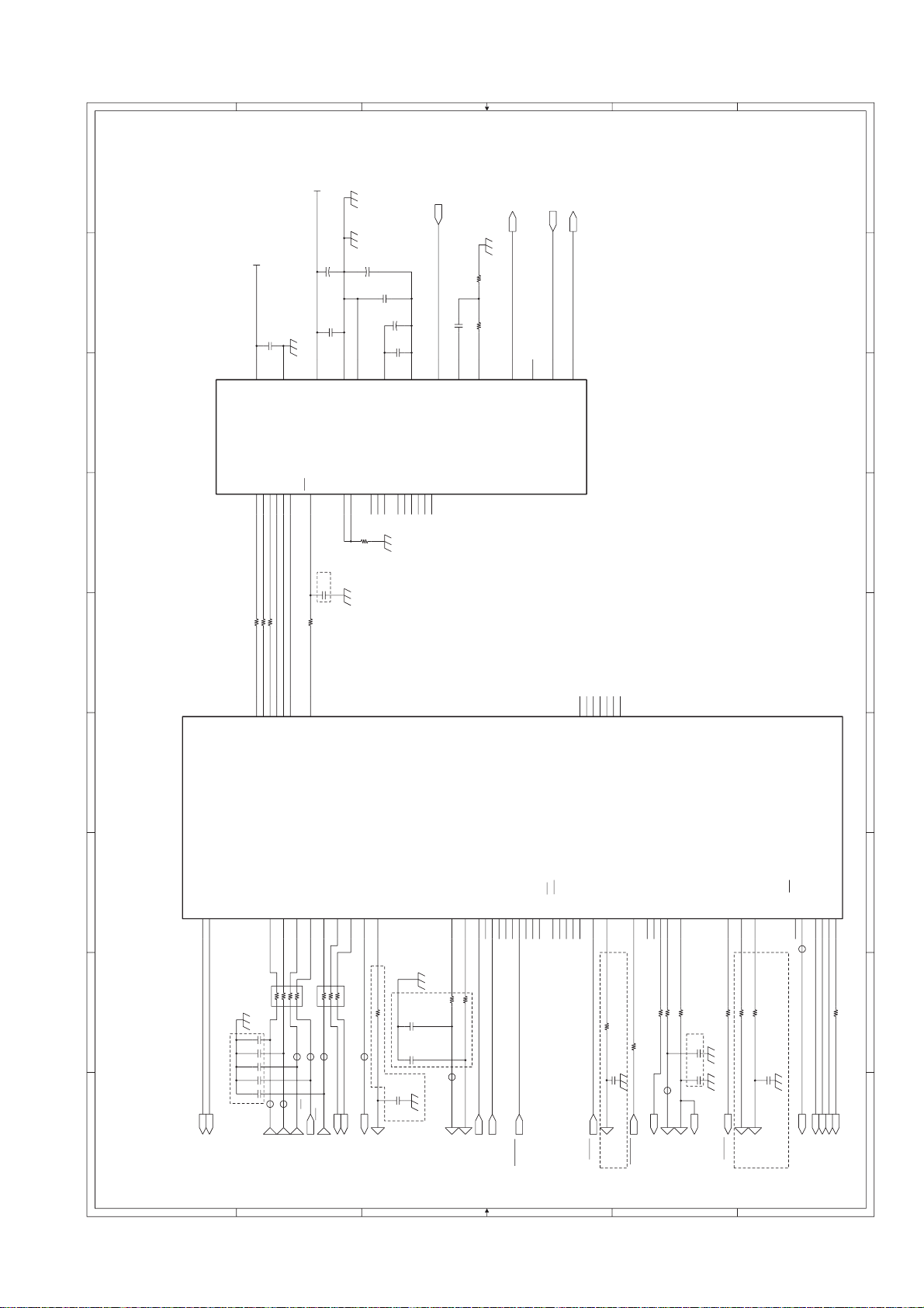
UX-510UA
A
A
B
B
C
C
D
D
E
E
F
F
G
G
H
H
I
I
6 6
5 5
4 4
3 3
2 2
1 1
C222
N.M.
R202
0
R149
R137 0
C217
IC 13
20415
FSYNC6ICLK26MCLK31CTRLSIN1SIN5SOUT4POR7MODE024MODE123RESERVED2RESERVED3RESERVED22NC25NC27NC28NC29NC30NC
32
DVDD
21
DVSS
20
AVDD
15
AVSS16AVSS
8
VREF
13
AGND
14
MICIN+
10
MICIN-
11
MICBAIS
12
SPKRO+
18
SPKRO-
19
LINEIN
9
LINEO
17
C103
RA 13
270
R135 270
R203 270
C15
10/50
+
R132 0
R204 270
C14
10/50
+
C12
10/50
+
R200
1K
R213
0
R201
2.2K
C208
R146 470
R172 270
R101 270
RA 12
270
123
4
876
5
123
876
C167
C204
N.M.
C203
R138
C212
C215
C200
R150
R144
1K
C201
N.M.
C205
R147
R145
C176
0.1
C199
R148
C198 0.1
C197
0.1
C221
0.1
C220
0.1
IC 9
SCE114(2/2)
GPIO37
142
GPIO36
138
GPIO25
122
GPIO26
123
GPIO27
124
GPIO28
125
GPIO29
131
GPIO30
132
GPIO31
133
GPIO32
134
GPIO33
135
GPIO34
136
GPIO35
137
GPIO1256GPIO1355GPIO1454GPIO1553GPIO1652GPIO1751GPIO18
107
GPIO19
39
GPIO1
110
GPIO2
109
GPIO3
108
GPIO4
57
GPIO564GPIO663GPIO762GPIO8/FWR
112
GPIO9/FRD
111
GPIO1065GPIO11
40
GPIO0
140
GPO0
165
GPO1
164
GPO2
163
GPO3
162
GPO22/VIDCNT1
113
GPO23/FCS/VIDCOTL0
114
GPO26
126
GPO27
127
GPO28
128
GPO29
129
GPO30
130
GPO31
141
NC60NC
81
NC34NC35NC36NC37NC
38
SA1CLK
149
IA1CLK
145
IACLK
144
SR1IO
148
SR4OUT
147
SR3IN
146
IARESET
143
+3.3V
+5.0V
SIGTX
SIGRX
SIGMUTE
DTMFMUTE
CNLIUA-1
CNLIUA-6
CNLIUA-5
CNLIUA-10
SPMUTE
RCVOL
CNLIUB-2
CNLIUB-4
CSWI
DRSNS
ORGSNS
VOL-B
VOL-C
VTHON
CNLIUA-4
CNLIUA-7
CNLIUB-3
CNLIUB-1
CNPW-7
VOL-A
LEDON
SPOUT
TELOUTI
CNLIUB-5
PINSNS
FRSNS
RBNSNS
CML
VIDCNT1
PNLON
GCONT
(6-2E)
(6-4D)
(6-5E)
DG
CIHSPE1
PIN
RHS
SPMUTE
SIGMUTE
DTMFMUTE
DG
TXMUTE
RCVOL
DPMUTE
ERLY
DG
PSAVE
DG
DG
DG
TELMUTE
CML
DG
RLYCONT
DPON
DG
DG
DG
DGMAG
MAG
(6-4D)
(6-1E)
(4-4D)
(6-4F)
(6-1E,5E)
(4-6D)
(4-3D)
(4-3D)
(4-5D)
(5-4F)
(6-2E)
(6-2F)
(5-3E)
(6-2F)
(6-2F)
(6-4F)
(5-1A)
(1-2A)
(4-5D)
N.M.
N.M.
N.M.
N.M.
(5-6A)
GCONT
FO-1470U
Modem block 3/6
6 – 3
Page 66
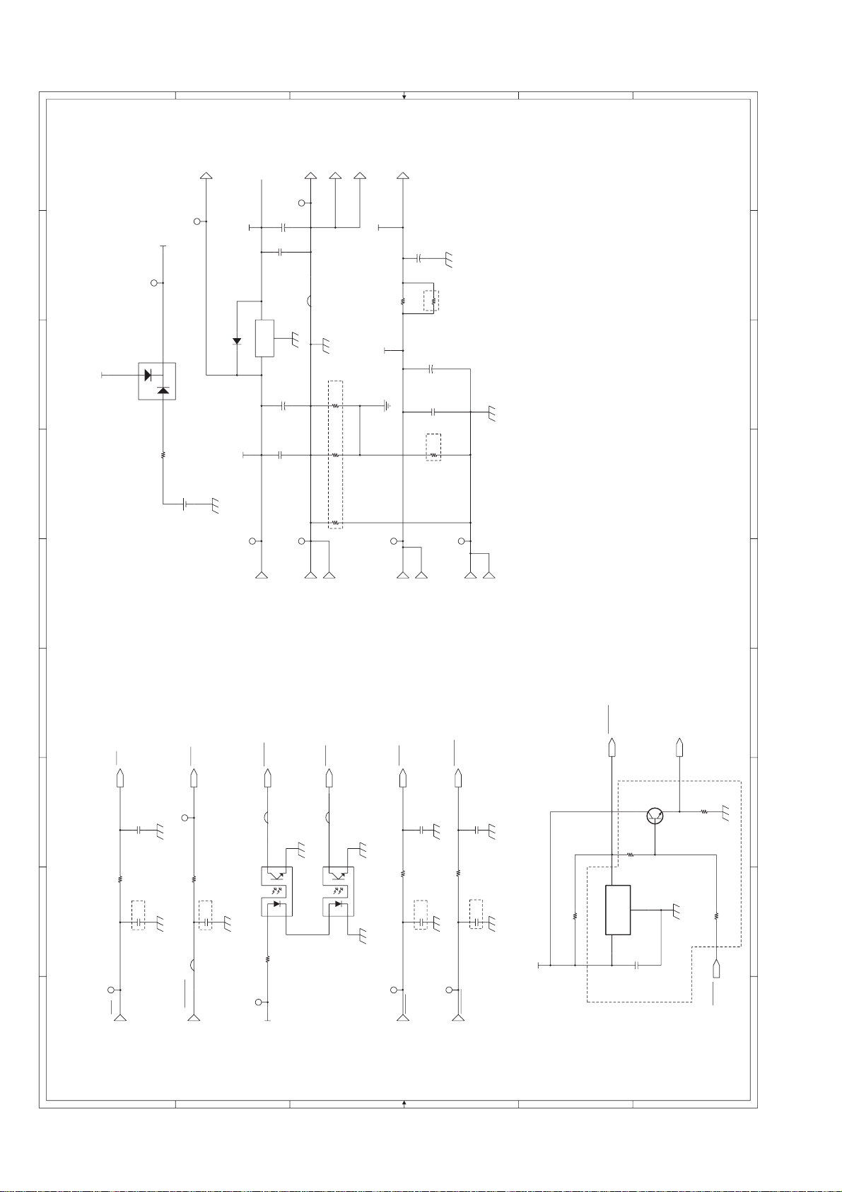
UX-510UA
A
A
B
B
C
C
D
D
E
E
F
F
G
G
H
H
I
I
6 6
5 5
4 4
3 3
2 2
1 1
R206
270
R205
0
R174
N.M.
R109
270
C105
100P
R108
270
C107
100P
C 13
100/50
+
R100
N.M.
R216
N.M.
R215
R103
C 1
47/25
+
C 5
220/6.3
+
C 2
22/50
+
C102
1
C104
0.1
C111
1
<VBT>
<DG>
<DRSNS>
<RBNSNS>
PI 2 (INK)
SG206S
1
2
4
3
<+24V>
<DRSNS>
PI 1(P-IN)
SG206S
1
2
4
3
<PINSNS>
Q 103
B
C
E
IC 100
XC61AN
VCC
3
GND
2
OUT
1
BAT1
CR2032
+
D 102
HRW0202
A1
A2 K
R122
R112
R121
R120
51K
C108
C181
N.M.
C106
N.M.
C119
N.M.
C202
N.M.
C180
100P
REG1
XC62FP3302P
IN
3
OUT
1
G
2
D 101
1SS355
R107
5.6K
R 1
1K (1W)
R173
270
+24V
+3.3V
+3.3V
VBAT
+24V
+5V
+24VA
+3.3V
RBNSNS
CSWi
DRSNS
FRSNSi
ORGSNSi
PWRDWNI
CNPN-8
CNPN-9
CNPW-5
CNPW-6
CNPW-8
CNPW-1
CNPW-2
CNPW-3
CNPW-4
CNLIUA-12
CNLIUA-13
CNPN-5
CNCSW-2
CNLIUA-14
CE2
RESETO
CNCSW-1
CNLIUA-11
PINSNS
CSW
DG
DG
DG
DG DG
FRSNS
ORGSNS
DG
DG
DGA
DG
DG
MG
FG
+5V
DG
DG
+24V
+24V
+5V
DG
DG
DG
MG
MG
+24VA
DG
(3-4A)
(4-3A)
(3-2A)
(3-3A)
(3-3A)
(1-1H)
(2-4D)
DG
DG
DG
DG
(3-5A)
DOOR SW
DG
N.M.
(5-5B)
VREF
FO-1470U
Sensor/Reset/Power supply block 4/6
6 – 4
Page 67
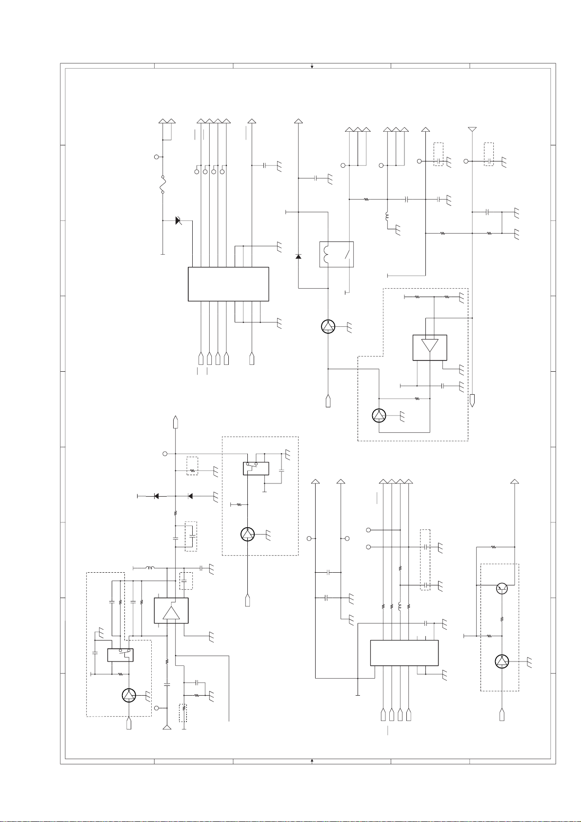
UX-510UA
A
A
B
B
C
C
D
D
E
E
F
F
G
G
H
H
I
I
6 6
5 5
4 4
3 3
2 2
1 1
Q101
B
C
E
IC 1
TD62001
E
8
1B12B23B34B45B56B67B
7
7C106C115C124C
133C142C151C16
COM
9
<VIN>
<VO>
FU100
KAB2402
D1
1N4748
C166
C165
N.M.
<VG>
R155
470
270
R153
C193
270
R152
R154
470
L112
0
R176
33K
R177
C182
0.1
HCT04
IC10
1A12A33A
54A9
5A116A
13
1Y22Y43Y64Y85Y106Y
12
VCC
14
GND
7
R197
D104
1SS355
D103
1SS355
C162
N.M.
C153
N.M.
C101
1
R160
100
C4
100/50
+
C3
10/50
+
L116
0
R175
1K
Q113
B
C
E
C194
R167
C183 15P
R178
4.7K
1
C223
C8
22/50
+
C154
0.1
C184
N.M
C9
N.M.
+
C7
100/50
+
R187
N.M
C224
1000P
C125
0.1
Q102
BC
E
R106
0R110
R111
IC7
2
1
53
4
R139
22K
R151
20K
R102
470K
RY1
OJE-SH-124M
43
12
D100
1SS355
Q100
DTC143ZK
B
C
E
Q108
BC
E
L101
0
NJM318
IC 11
3
2
6
7
4
1
5
8
+
–
V
–
V+
BC3
BC1
BC2
R199
IC6
3
1
425
+
–
V+
GND
C185
0.1
C226
R219
C227
0.1
Q114
B
C
E
R217
C225
R218
IC12
2
1
53
4
+5V
+24V
+24V
+24V
+5V
+5V
+3.3V
+5V
+5V
+3.3V
+5V
+3.3V
+5V
+24V
VIN
TPA
TPB
TPB
CNCCD-1
CNLED-1
CNMT-5
CNMT-6
CNMT-4
CNMT-3
CNMT-2
CNMT-1
CNTH-1
CNTH-2
CNTH-16
CNTH-7
CNTH-8
CNTH-9
CNLED-2
LEDON
TPA
CNCCD-7
CNCCD-6
CNCCD-4
CLK1
CLK2
START
CNCCD-2
CNCCD-3
PNLON
CNTH-10
CNTH-5
CNPN-7
VIDCNT1-A
CNCCD-5
CLK1
VTHON
THADI
GCONT
DG
VO
+24V
MG
MG
VMT
VMT
TPAD
TPBD
TPAD
TPBD
MGMGMG
MG
VTH
VTH
VTH
DG
THVDD
(1-1G)
(3-2A)
(1-1E)
(1-1E)
(1-1F)
(1-1F)
MG
LEDON
DG
DG
ΦT
ΦRΦ1Φ2
ΦRΦT
DG DG
(3-1A)
(1-4A)
(1-4A)
(1-4A)
VCCD
VG
VG
DG
(3-2A)
DG
+5VPN
N.M.
DG
DG
(1-1F)
DG
THG
THI
THG
(1-1A)
DG
DG
DG
DG
DG
(1-4A)
(CLK1)
(CLK1)
N.M.
DG
DG
DG
DG
N.M.
DG
DG
DG
(3-5B)
N.M.
DG
N.M.
VREF
(4-5I)
FO-1470U
Video processing/Motor drive / Thermal block 5/6
6 – 5
Page 68
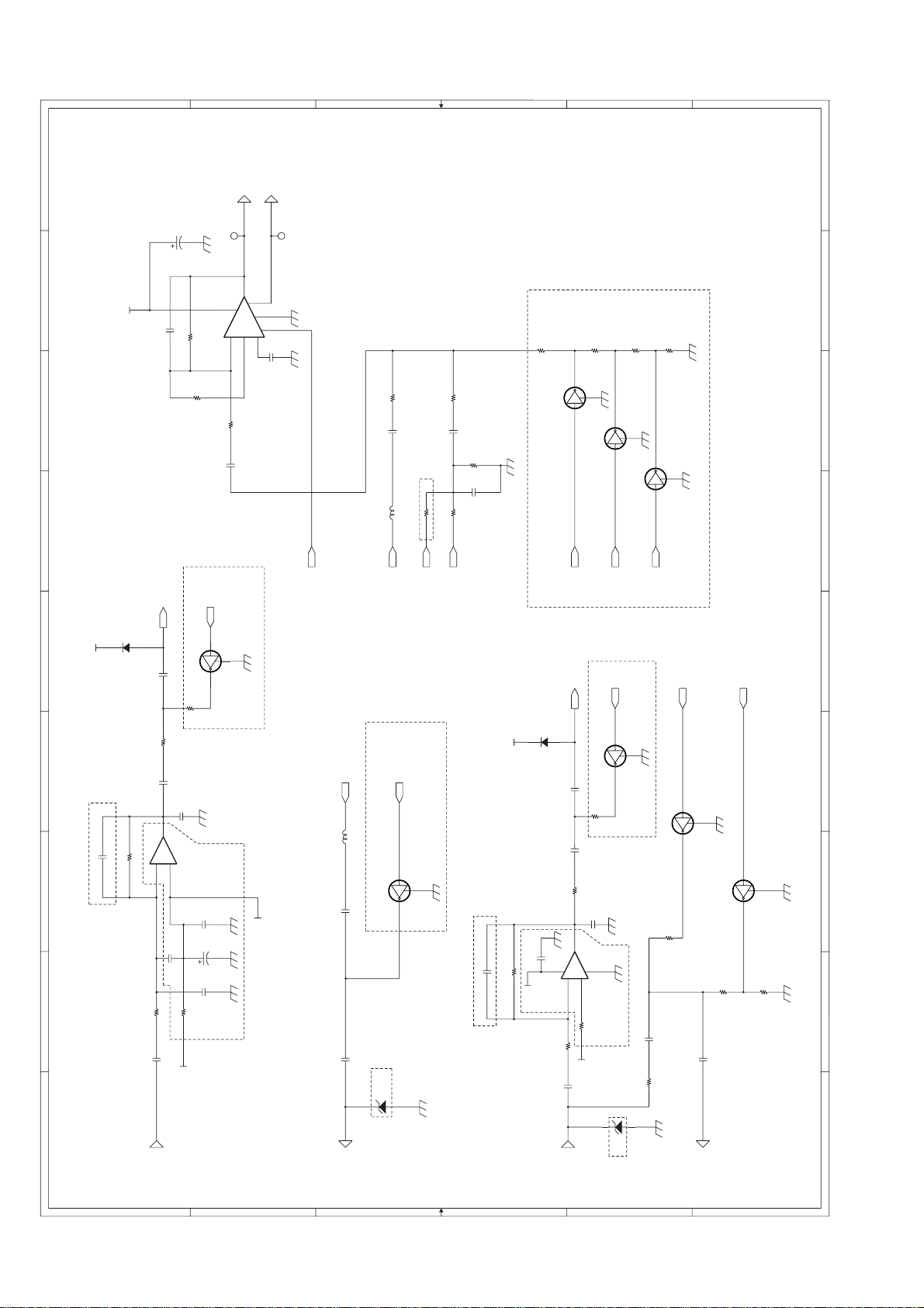
UX-510UA
A
A
B
B
C
C
D
D
E
E
F
F
G
G
H
H
I
I
6 6
5 5
4 4
3 3
2 2
1 1
C191
0
C186
0
R180
0
R185
220P
R163
0
R196
43K
C168
0
C190
1
R186
R161
R212
220K
R195
3K
R190
100K
ZD100
N.M.
C218
220P
C192
1
C219
1
C189
0.1
D106
1SS355
Q107
B
C
E
ZD101
N.M.
C171
1
L118
0
R182
4.7K
Q104
RNC1402
B
C
E
C196
0
Q110
BC
Q111
BC
Q112
B
C
E
E
E
R193
R192
R194
R191
C210
Q106
B
C
E
L119
0
C209
R168
20K
R164
100K
R169
C211
C170
4700P
R166
1K
R181
0
IC14
3
2
1
+
–
D105
1SS355
C169
0.01
C206
Q105
RNC1402
B
C
E
IC 14
5
6
7
4
8
+
–
C187
N.M.
R183
11K
184
100K
Q109
B
C
E
NJM2113
IC 15
5
432
1
7
8
6
–
+
C216
1
C207
0
C213
C214
0
R207
0
R209
220P
R208
0
R162
C11
47/25
12
C10
12
R210
0
R211
R179
39K
C188
0.1
+5VA
+5VA
+5V
+5V
+5V
+5V
+24VA
CNLIUA-8
SIGRX
CNLIUA-3
CNSP-1
CNSP-2
SPMUTE
SIGTX
RCVOL
TELOUT1
CNLIUA-2
CNLIUA-9
RCVOL
CML
SIGMUTE
SPOUT
BZOUT1
BZOUT2
VOLC
VOLB
VOLA
DTMFMUTE
TELOUT
DG
DG
SP+
SP
–
TELIN
DG DG
DG
DG
RXIN
DG
DG
DG
DG
DG
DG
DG
DG
DG
DG
(3-3I)
(3-4A)
(3-5A)
(3-6A)
(3-2A)
(3-4I)
(3-3I)
(3-6A)
(3-4A)
DG
TXOUT
(1-1F)
(1-1F)
DG
(3-3I)
(3-1A)
(3-1A)
DG
(3-1A)
DG
DG
DG
N.M.
N.M.
N.M.
N.M.
N.M.
N.M.
N.M.
N.M.
FO-1470U
Analog signal block 6/6
6 – 6
Page 69
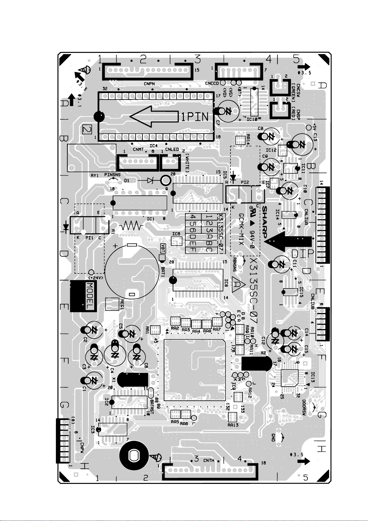
Control PWB parts layout (Top side)
UX-510UA
FO-1470U
6 – 7
Page 70
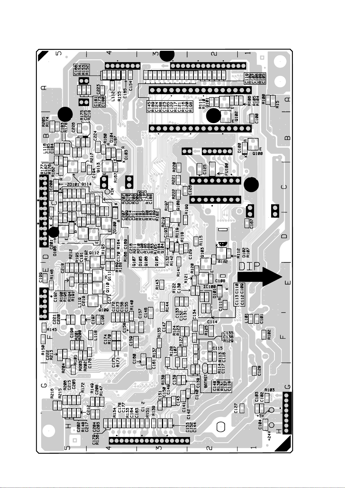
UX-510UA
FO-1470U
Control PWB parts layout (Bottom side)
6 – 8
Page 71
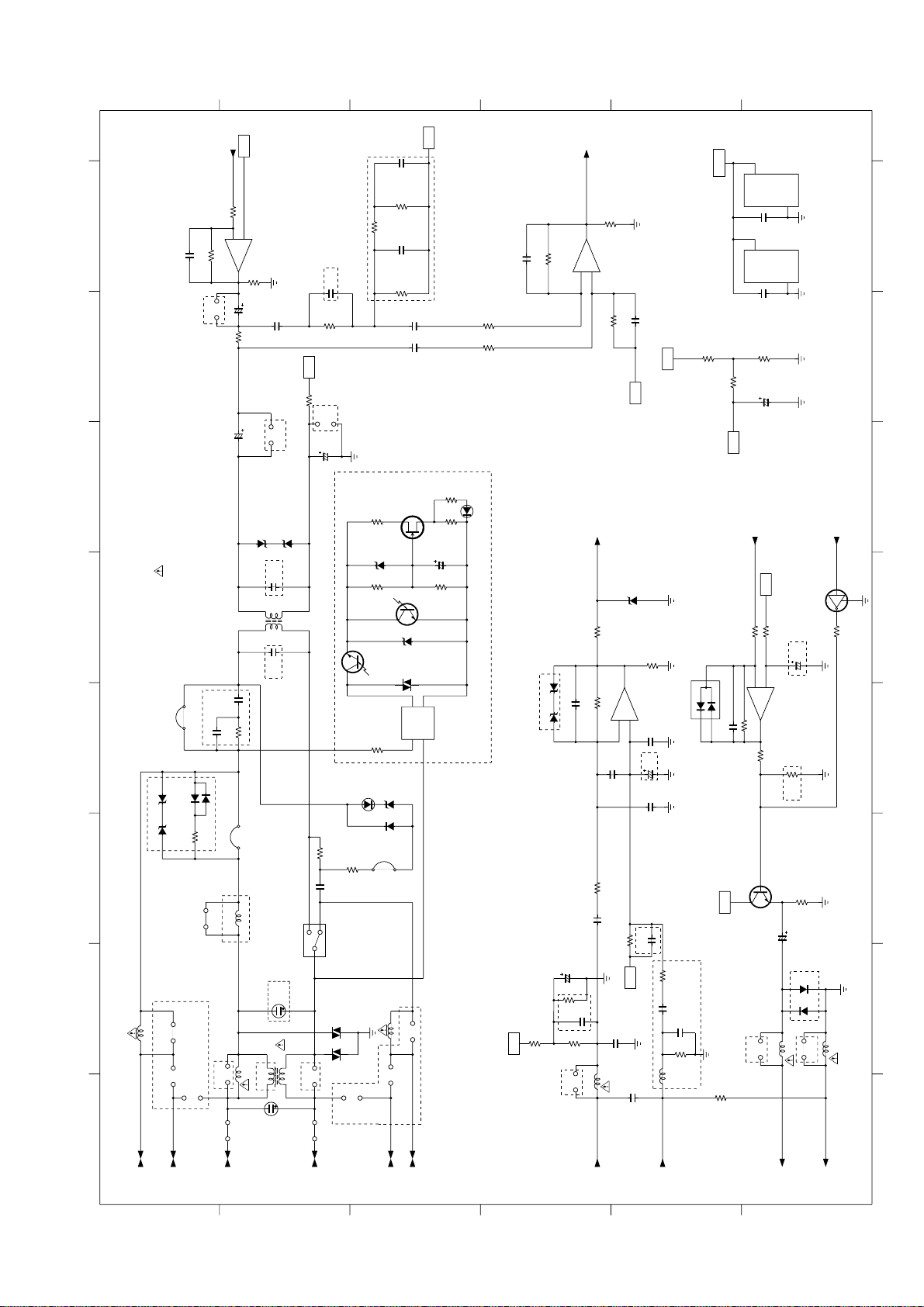
UX-510UA
1
2
6
4
3
5
BDEFG
I
HCA
BDEFG
I
HCA
1
2
6
4
3
5
–
+
+5VA
+5VA
–
+
+5VA
+24VA
+5V
VREF
+5VA
–
+
+5V
–
+
VREF
VREF
TLJ-2
CNLNJ-2
L9
R-5C
JP17JP12
JP11
CNLNJ-3
JP10
JP8
CNLNJ-4
VA3
ERZV5D471
VA2
ERZV5D471
ARG
CNLNJ-5
JP4
TLJ-1
JP3
L1
R-5C
JP1
JP16
L8
N.M.
L2A
N.M.
N.M.
C
M
B
CML1
C8
0.82
R111
22K
R5
22K(1/2W)
D2
1SS133
ZD6
HZ27C
PC4
TLP521
C15
R119
C14
N.M.
2
1
4
3
T1
I2164
C7 C111
N.M.
N.M.
~
~
+
–
REC1
PC3
PC2
R104
ZD3
R103
C3
R4
R2
PC1
R1
D
G
S
Q1
R6
N.M.
ZD4
HZ2C1
ZD5
HZ2C1
JP6
C5
22/50
JP7
DG
+5V
C6
22/50
R118
100
R116
620
JP5
C4
4.7/50
C108
0.039
C107
N.M.
R114
300
7
6
5
R121
1K
DG
C114
33P
R122
86.6K
IC101
2904
R117
4.7K
TXOUT
CNLIUA-8
R107
C104
R110
C105
R109
N.M.
C106
1
C113
1
R112
20K
R120
20K
R115
47K
C112
820P
C109
33P
R113
15K
2
3
1
IC101
2904
RXIN
CNLIUA-9
R108
3.3K
DG
8
4
DG
C118
0.1
C110
0.1
8
4
DG
IC102
2904
IC101
2904
R139
20K
R138
20K
R140
0
C10
10/50
DGDG
CNHJ-4
CNHJ-1
TX+
TX
–
C127
2200P
CNHJ-2
CNHJ-3
RX+
RX
–
R130
1.5K
R128
1K
C9
22/50
DG
C117
2200P
DG
C123
0.1
R134
1K
ZD9 ZD8
N.M.
C124
0.01
R135
10K
C125
220P
R136
3.3K
C126
1000P
C12
C119
1000P
DGDGDG
N.M.
IC102
2904
1
2
3
R133
0
TELOUT
CNLIUA-2
D4 D3
N.M.
DG
L5 R-5C
C13
22/50
R127
150
R126
N.M.
DG
DG
R124
3.3K
DG
7
6
5
IC102
2904
C115 220P
R125 220K
C11
N.M.
TELIN
CNLIUA-3
R132
39K
R131
8.2K
TELMUTE
CNLIUA-4
R123
0
DG
Q104
DTC143ZK
JP2
AR2
ZD2
DG
DG
Q105
2SC2412K
JP9
N.M.
N.M.
N.M.
N.M.
JUMPER
R8
R9
R7
PC5
ZD10 ZD11
N.M.
N.M.
N.M.
L3
R-5C
L2B
R-5C
N.M.
AR1
RA-391P
JUMPER
ZD1
JUMPER
VA1
D101
DA204K
ZD7
MTZJ5R1B
C122
R141
0
N.M.
R142C128
DG
C129
R143
L6
N.M.
R137
0
L7 R-5C
JP14
N.M.
JP15
N.M.
JP13
N.M.
L4
R-5C
R129
C116
N.M.
NOTE:
THESE MARKS ARE ALL SAFETY - CRITICAL PARTS.
FO-1470U
[2] TEL/LIU PWB circuit 1/2
6 – 9
Page 72
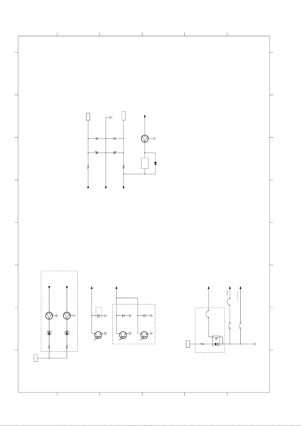
UX-510UA
1
2
6
4
3
5
BDEFG
I
HCA
BDEFG
I
HCA
1
2
6
4
3
5
+5V
DPON
CNLIUB-1
DPMUTE
CNLIUB-2
R101
PC3
Q103
DG
Q101
DG
R102
PC2
HS
CNLIUA-6
DGDG
C121
PC5
DGDG
C103
PC1
N.M.
N.M.
RHS
CNLIUA-1
DG
CNLIUA-10
CNLIUA-11
CNLIUA-12
+5V
CNLIUA-13DGCNLIUA-14
+24V
R105
1K
C1
22/25
C2
22/50
C101
0.1
C102
0.1
+5VA
DG
+24VA
R106
100
CNLIUA-7
CML1
D1
1SS133
DG
Q102
DTC143ZK
CML
CI
CNLIUA-5
DGDG
C120
PC4
TLP521
N.M.
R3
+5V
PE1
TP1
TP2
A
K
C
E
SW2
HOOK SW
SW1
HOOK SW
DOOR SW
PE1
N.M.
FO-1470U
TEL/LIU PWB circuit 2/2
6 – 10
Page 73
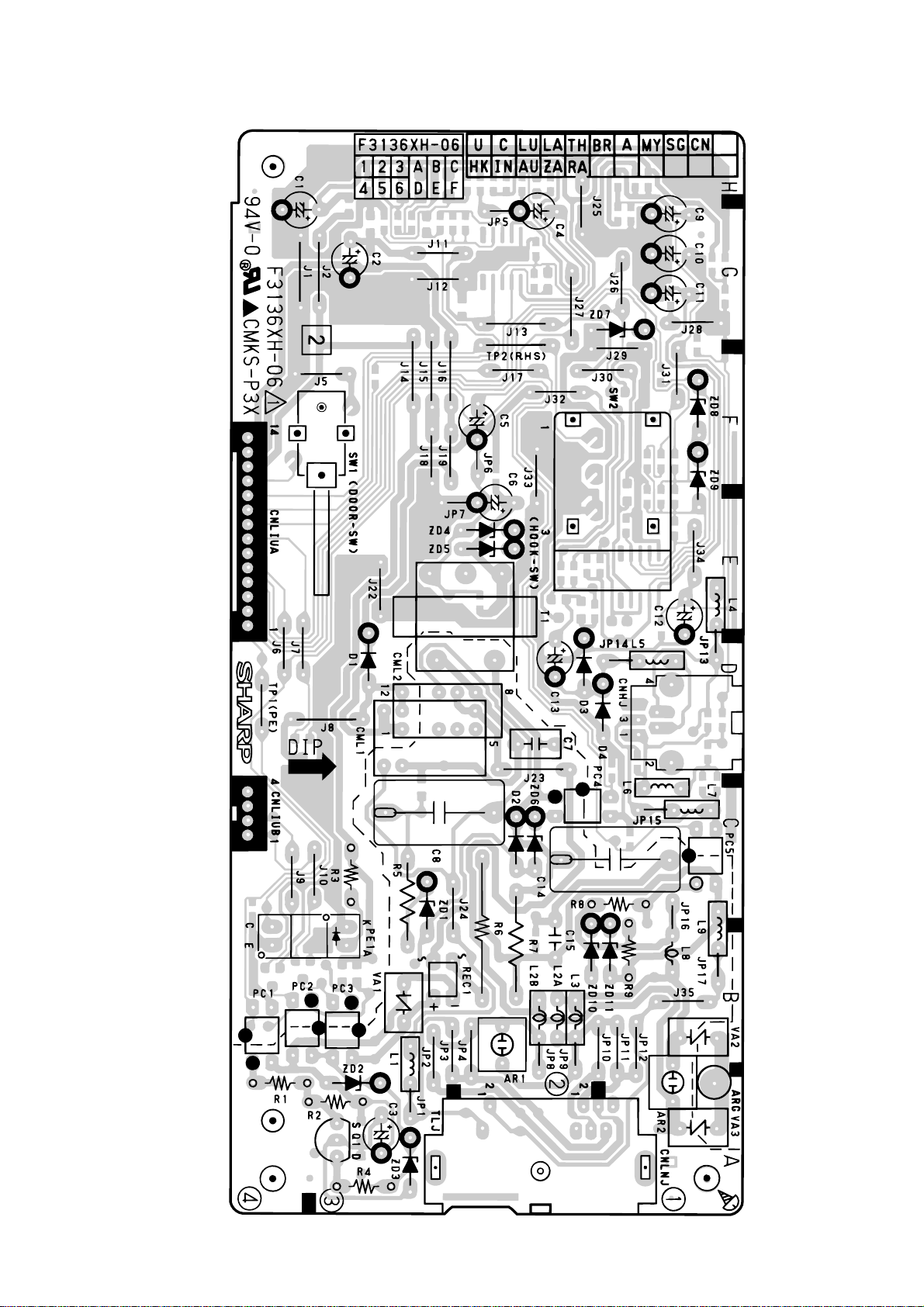
TEL/LIU PWB parts layout (Top side)
UX-510UA
FO-1470U
6 – 11
Page 74
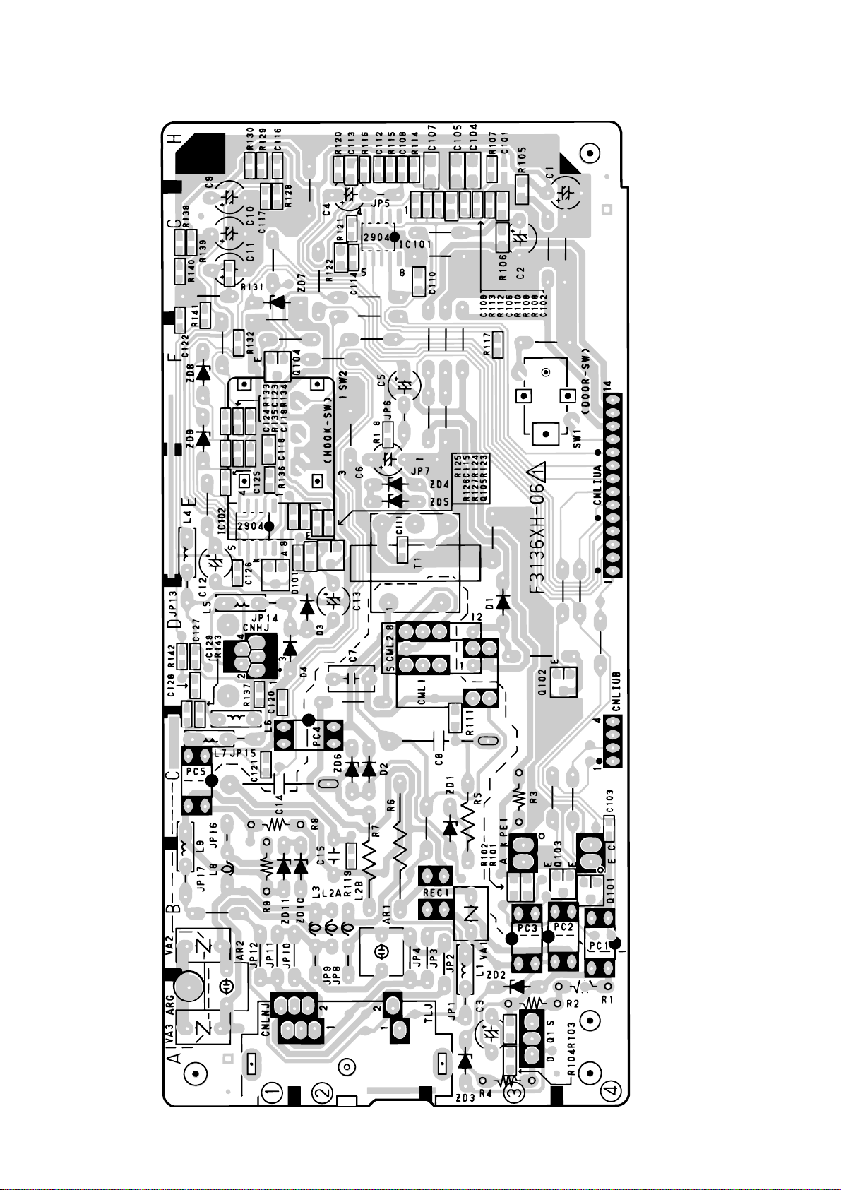
UX-510UA
FO-1470U
TEL/LIU PWB parts layout (Bottom side)
6 – 12
Page 75
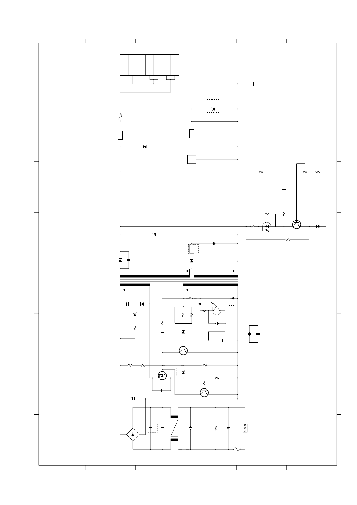
UX-510UA
1
2
6
4
3
5
BDEFG
I
HCA
1
2
6
4
3
5
BDEFG
I
HCA
R7
180
N.M.
C24
270P
C23
4700P
FB2
JUMPER
D7
S3L20U
C13
1500P
T1
PTTN117
ZD4
RD30FB3
IC1
UPC78M05
F3
CCP2E100
C16
0.1
R16
22K
C12
0.1
R15
330K
R14
1K
R13
4.7K
PC1
PC2501-1L
R18
3.3K
Q4
2SC1740
ZD5
RD6.2SB
VR1
1K
R17
8.2K
C10
330/16
D8
AK04-V0
R4
560
D9
ERA22-06-V3
R24
100K
C4
1500P
ZD2
RD4.3SB2
ZD6
JUMPER
D5
1SS355
C6
0Ω
PC1
PC2501-1L
C17
1000P
C5
4700P
R7
180
D6
R2
470K
R3
470K
Q1
FS5KM-14
C3
680P
ZD1
Q2
2SC4115
Q3
2SC1741
R9
470
R10
0.15(1W)
R8
47K
CN1
F1
2.5A/125V
C1
0.1
1
3
V1
S07K150GA
L1
ELF15N005
C15
DS1
S1WB60
N.M.
CN2
1
2
3
4
5
6
+24V
+24V
GND
GND
+5V
GND
C2
150/220
C8
330/35
R5
6.8K
R6
47K
R1
2.2M(1/2W)
49
6
2
3
12
11
10
N.M.
ZD8
C25
0.1
N.M.
C26
3300P
C7
N.M.
FB1
BL02RN1
FB1
OPTION
FO-1470U
[3] Power supply PWB circuit
6 – 13
Page 76
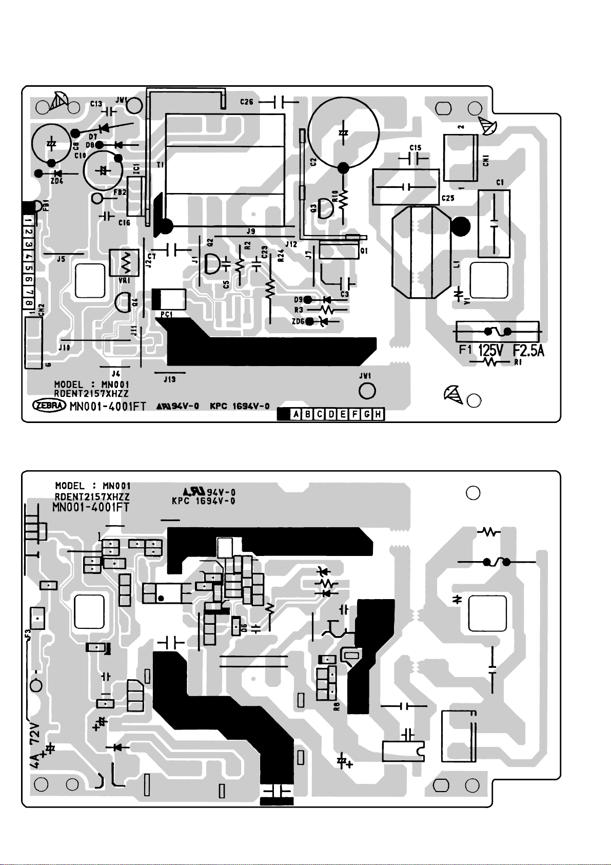
UX-510UA
FO-1470U
Power supply PWB parts layout (Top side)
Power supply PWB parts layout (Bottom side)
ZD5
C12
R16
R17
ZD8
R18
J14
R15
R14
R13
D5
R7
C17
C24
R5
R6
ZD2
R4
C6
C4
ZD1
R9
6 – 14
D51
Page 77
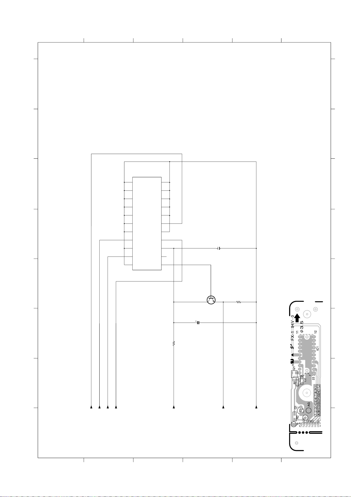
UX-510UA
1
2
6
4
3
5
BDEFG
I
HCA
1
2
6
4
3
5
BDEFG
I
HCA
IC1
TCD1208AP
CN1-6
CN1-5
CN1-4
CN1-7
Φ1Φ2ΦTΦ
R
22
21
20
19
18
17
16
15
14
13
12
1
2
3
4
5
6
7
8
9
10
11
NC
NC
NC
NC
NC
Φ1
NC
RS
OD
DOS
OSSS
SH
NS
Φ2
NC
NC
NC
NC
NC
NC
NC
NC
Q1
C1815
C2
0.022
CN1-2
+5V
CN1-1
VO
CN1-3
AG
C1
22/50
R1
2.2K
R2
39
V0
1
5V
F2802XH-Z8
FO-1470U
[4] CCD PWB circuit
CCD PWB parts layout
6 – 15
Page 78
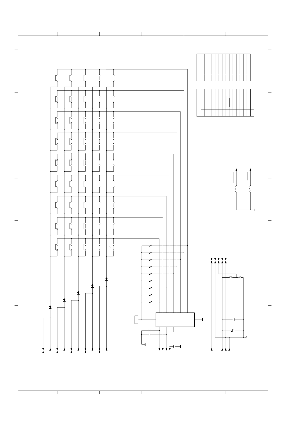
UX-510UA
1
2
6
4
3
5
BDEFG
I
HCA
1
2
6
4
3
5
BDEFG
I
HCA
D1D2D3D4D5D6D7D8D9
1112131234510
A0A1A2
A3
VCC
GND
976
14
15
8
IC1
74HC147
CNPN
KEN 4A1
34567
8
9
101112
13
KEN 3A
KEN 2A
KEN 1A
GND
GND
+5V
ORGSNS
FRSNSESEN4
SEN3
SEN2
CNPN-15
CNPN-14
CNPN-13
CNPN-12
CNPN-11
SEN0
SEN1
SEN2
SEN3
SEN4
CNPN-4
KEN 1A
CNPN-3
KEN 2A
CNPN-2
KEN 3A
CNPN-1
KEN 4A
CNPN-10
E
CNPN-6
GND
CNPN-5
GND
COPY
1
4
DOWN
3
6
9
UP
2
5
SPEED
REDIAL
HOLD
01
06
11
02
07
12
17
03
13
18
04
14
START
05
15
SHIFT
MEMORY
MODE
FUNCTION
STOP RESO
CNLCD-6
CNLCD-5
CNLCD-3
CNLCD-2
CNLCD-1
C2
22/50
C1
0.022
R10
6.2K
19
CNPN-7
+5V
08 09
10
16
CNLCD-11
LD4
CNLCD-12
LD5
CNLCD-13
LD6
CNLCD-14
LD7
CNLCD-4
RS
D1
1SS133
D2
1SS133
D3
1SS133
D4
1SS133
D5
1SS133
#
0
78
SPEAKER
+5V
16
N.C
R1
100K
R2
100K
R3
100K
R4
100K
R5
100K
R6
100K
R7
100K
R8
100K
R9
100K
R11
1K
VO
ORGSNS
FRSNS
FRSNS
SW-169-65AU
CNPN-8
CNPN-9
14 SEN1
15 SEN0
CNLCD
GND1
2345678
9
1011121314
+5VVORS
R/WEN.C
N.C
N.C
N.C
LD4
LD5
LD6
LD7
ORGSNS
SW-169-62AU
2
NOTE: Since the parts of PWB cannot be supplied, change it as a unit.
C3
0.022
C5
0.022
C4
0.022
FO-1470U
[5] Operation panel PWB circuit
6 – 16
Page 79
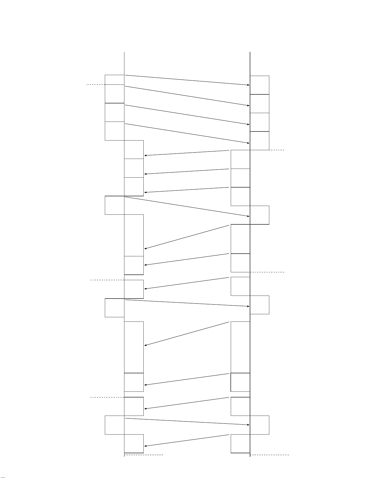
CHAPTER 7. OPERATION FLOWCHART
[1] Protocol
Receive side
G3 communication
Transmitter side
(Document inserted into
document sensor during
standby)
UX-510UA
FO-1470U
To recording
position
CED
NSF
CSI
DIS
(DCS)
CFR
TSI
NSS
TCF
IMAGE
SIGNAL
TSI
NSS
TCF
IMAGE
CED
NSF
CSI
DIS
Document inserted to
the reading position
(DCS)
CFR
1st page
SIGNAL
Cut line printed
Cut line printed
MCF
MCF
RTC
MPS
IMAGE
RTC
EOP
SIGNAL
RTC
MPS
IMAGE
RTC
EOP
Next page insert
command
MCF
SIGNAL
MCF
DCN
DCN
Document ejectedRecording paper ejected
7 – 1
Page 80
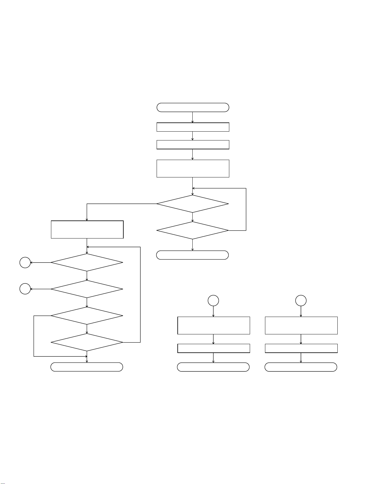
UX-510UA
FO-1470U
[2] Power on sequence
START
CPU initialized
MODEM initialized
“WAIT A MOMENT” display
STOP key ?
NO
“MEMORY CLEAR ?” display
YES
1
YES
2
YES
START key ?
NO
COPY key ?
NO
STOP key ?
NO
3 sec ?
YES
STAND-BY
NO
3 sec ?
YES
STAND-BY
“MEMORY CLEARED” display
Memory clear
STAND-BY
NO
21
“MEMORY CLEARED” display
Memory clear
PROCESS CHECK MODE
7 – 27 – 2
Page 81
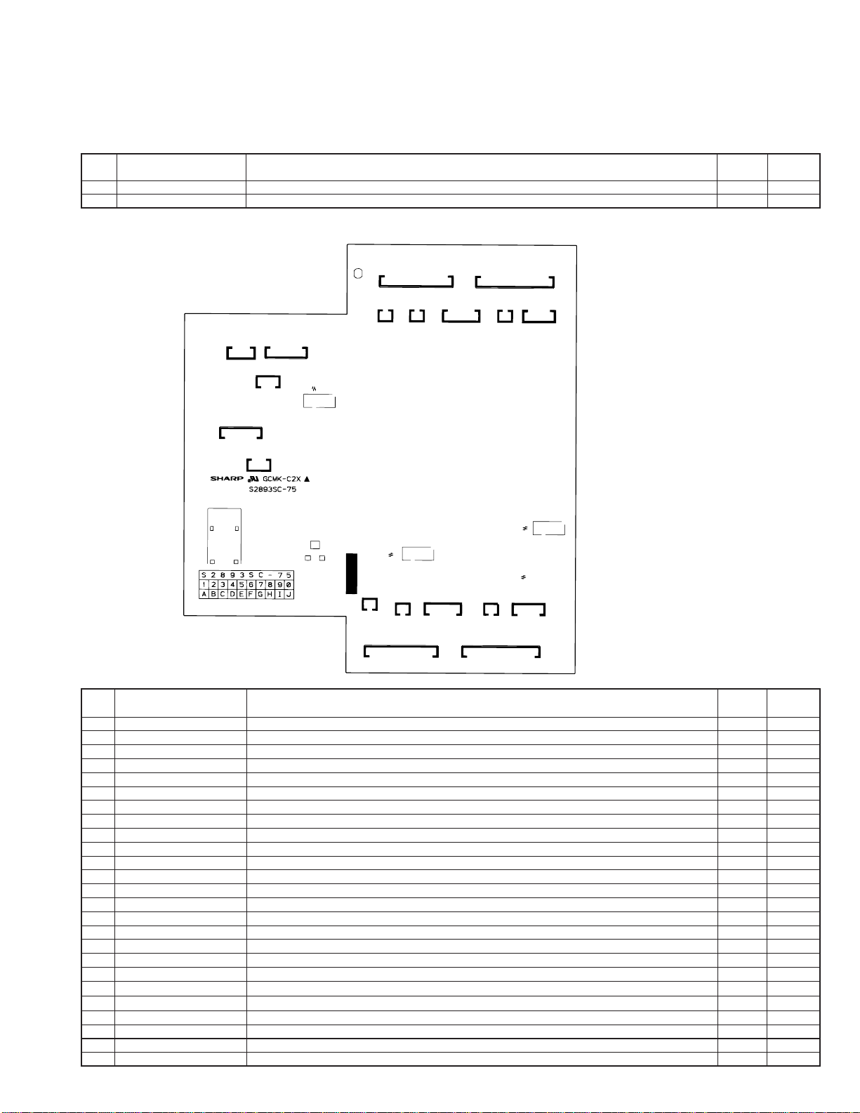
UX-510UA
FO-1470U
CHAPTER 8. OTHERS
[1] Service tools
1. List
NO. PARTS CODE DESCRIPTION Q’TY
1 C P W B S 2 8 9 3 S C 0 2 Extension board unit 1BZ
2 U K O G M 2 0 5 7 S C Z Z Optical adjustment jig 1BR
Extension board unit
PRICE
RANK
1
CNSNS
CNPH1
8
HOOK SW
1
CNBZ1
4
36
25
14
51
CNBZ2
1
CNPH2
4
1
8
R1
2
A
K
PE
DOOR SW
1
11
CNPN2
111
2
CNSP2
CNCS2
1
E
C
RBN
3
R2
2
CNSP1
15
1
2
AE
KC
1
CNCS1
2
1
CNPN1
2
CNCCD1
7
15
CNCCD2
16
1
CNTH2(*1)
7
1126
CNLED2
CNMT2
2
R3
1
1
R4
2
CNTH1(*1)
2
CNMT1
6
CNLED1
1
16
PIN
AE
KC
11
1
NOTE(*1): Mount connectors to
CNTH1 and CNTH2 in the reverse
direction against silk print of PWB.
NO. PARTS CODE DESCRIPTION Q’TY
PRICE
RANK
1 Q C N W – 4 7 2 3 S C Z Z CABLE [CNPN2] 1AL
2 C C N W – 4 7 5 9 S C 0 1 CABLE [CNTH2] 1AX
3 Q C N W – 4 7 2 5 S C Z Z CABLE [CNCCD2] 1AH
4 Q C N W – 4 7 2 6 S C Z Z CABLE [CNMT2] 1AH
5 Q C N W – 4 7 2 7 S C Z Z CABLE [CNLED2] 1AF
6 Q C N W – 4 7 2 8 S C Z Z CABLE [CNSP2] 1AF
7 Q C N W – 4 7 2 9 S C Z Z CABLE [CNCS2] 1AF
8 Q C N W – 4 7 3 0 S C Z Z CABLE [CNSNS] 1AH
9 Q C N W – 4 7 3 1 S C Z Z CABLE [CNPH2] 1AN
10 Q C N W – 4 7 3 2 S C Z Z CABLE [CNBZ2] 1AH
11 Q C N C M 2 4 0 1 S C 0 B CONNECTOR [CNSP1, CNSP2] 2AA
12 Q C N C M 2 4 4 2 S C 0 B CONNECTOR [CNCS1, CNCS2] 2AB
13 Q C N C M 7 0 1 4 S C 0 B CONNECTOR [CNLED1, CNLED2] 2AD
14 Q C N C M 7 0 1 4 S C 0 E CONNECTOR [CNSES] 1AB
15 Q C N C M 7 0 1 4 S C 0 F CONNECTOR [CNMT1, CNMT2] 2AB
16 Q C N C M 7 0 1 4 S C 0 G CONNECTOR [CNCCD1, CNCCD2] 2AB
17 Q C N C M 7 0 1 4 S C 1 E CONNECTOR [CNPN1, CNPN2] 2AC
18 Q C N C M 7 0 1 4 S C 1 F CONNECTOR [CNTH1, CNTH2] 2AD
19
Q C N C M 7 0 1 4 S C 0 D CONNECTOR [CNBZ1, 2]
20
Q C N C M 7 0 1 4 S C 0 H CONNECTOR [CNPH1, 2]
2
2
AB
AB
21 V H P S G 2 0 6 S / / - 1 PHOTO TRANSISTOR [P.E, RBN, PIN] 3 AG
22 V R D - R C 2 E Y 0 0 0 J RESISTOR (1/4W 0Ω ±5%)[R4] 1AA
23 V R D – R C 2 E Y 2 2 1 J RESISTOR (1/4W 220Ω ±5%) [R1, R2, R3] 3 AA
24 Q S W - Z 2 2 0 6 S C Z Z HOOK SWITCH 1AH
25 Q S W - Z 2 2 2 6 S C Z Z DOOR SWITCH 1AG
8 – 1
Page 82
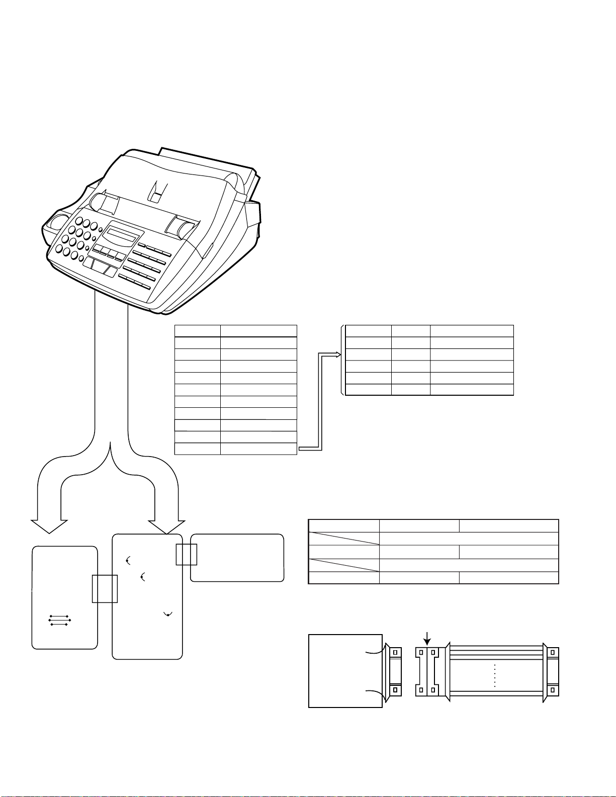
UX-510UA
FO-1470U
2. Description
2-1. Extension board unit
1. Remove the TEL/LIU PWB, control PWB and Power Supply PWB
from this unit, and mount the extension board unit instead.
• Before connecting the wiring to the extension board unit, set the
test PWB switches to the fixed position.
2. The setting is as follows.
A set with a mounted
extension board unit
J17
J13
CNLIUA
14
TP2
1
Cable
CNPW
DOOR SW
RBNSNS
CNLIUA
PINSNS
Connector Cable
CNPN2
CNTH2
CNCCD2
CNMT2
CNLED2
CNSP2
CNCS2
CNPH2
CNBZ2
CNSNS
QCNW-4723SCZZ
CCNW-4759SC01
QCNW-4725SCZZ
QCNW-4726SCZZ
QCNW-4727SCZZ
QCNW-4728SCZZ
QCNW-4729SCZZ
QCNW-4731SCZZ
QCNW-4732SCZZ
QCNW-4730SCZZ
POWER
SUPPLY
PWB
Cable color CNSNS Connected to (PWB)
1. Brown RHS TP2 (TEL/LIU)
2. Red DRSNS DOOR SW (Control)
3. Orange N.C. —————
4. Yellow RBN
The hook switch are operated by OR of the mechanical unit switch and
the test PWB switch. When performing installation in the machine unit,
set the test PWB switches to the fixed position.
Mechanical unit PWB to be tested
Actual operation with mechanical unit
Hook SW
Hook SW
* Recording paper: ON
No recording paper: OFF
ON/OFF operation
PWB sensor check
ON-HOOK
RBNSNS (Control)
PINSNS (Control)5. Green PIN
ON-HOOK
ON/OFF operation
DON'T SEPARATE
CHECK
TEL/LIU
PWB
CHECK
CONTROL
PWB
UNIT
RELAY CABLE
Note: F or the thermal head cable only, connect to the relay cable, not to
the relay PWB.
8 – 2
Page 83
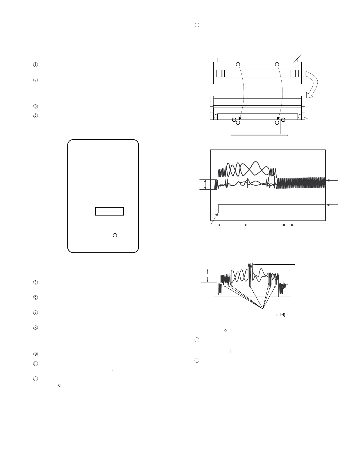
2-2. Scan optical system adjustment
(
)
(1) Outline
The adjustment procedures of the scan optical system are described
below:
(2) Adjustment procedures
1
Switch off the machine and disconnect the AC power cable from the
wall socket.
2
Fully open the upper cabinet, remove the fixing screws of the record-
ing paper tray and remove the recording paper tray. In order to perform a focus adjustment, remove the optical system unit from the
frame.
3
Disconnect the main PWB from the TEL/LIU PWB.
4
Connect your oscilloscope channel 1 to the VIN signal and channel 2
of your oscilloscope to φT signal (Refer Pin 4 of connector CNCCD
on the main pwb). Connect the earth clips of either probe to AG g round
as shown. Set the trigger to channel 2.
UX-510UA
FO-1470U
H
Lightly loosen the red screws of the CCD PWB and obtain the VID
signal wavefor m in synchronization with φT signal waveform. Adjust
the CCD PWB positioning to obtain the waveform as shown below.
Scan adjustment jig
Optical system
Reference surface
unit
VIN
(CH1)
CNCCD
VIN
VO CNCCD-3 (CCD source output)
øT CNCCD-6 (Line sync signal)
VG CNCCD-5
5
Re-connect the main PWB to the TEL/LIU PWB and connect these
circuit boards to the connectors on the chassis.
6
Re-assemble up to and including the recording paper tray to the main
chassis and close upper cabinet.
7
Plug the AC power cable into the w all outlet and turn the fax machine
on.
8
Insert a test char t in the document hopper and execute the CCD
Adjust Mode diagnostic. Press the START key to enable local copy
until approximately one fifth of the page has been copied, then press
the STOP key to enable the CPU wait state.
9
Fully open the upper cabinet and remove the recording paper tray.
F
Install the scan adjustment jig to the optical system unit, so that the
pattern surface is on the lower side.
G
Fit the pins of the scan adjustment jig to the holes of the optical sys-
tem frame.
Ground
1V/DIV
RøT
*1: Difference
CCD waveform
I
After completing the CCD adjustment, tighten the two red screws on
the CCD pwb and apply screw locking material to prevent the CCD
pwb from moving.
J
Assemble the recording paper tray and fixing screws.
1.89msec
0.5msec/DIV
*2: Black level
[CCD waveform model]
*2:White level
*1: Increase the difference
by focus adjustment.
*2: Adjust as shown by
CCD PWB adjustment.
ø
T
(CH2)
8 – 3
Page 84
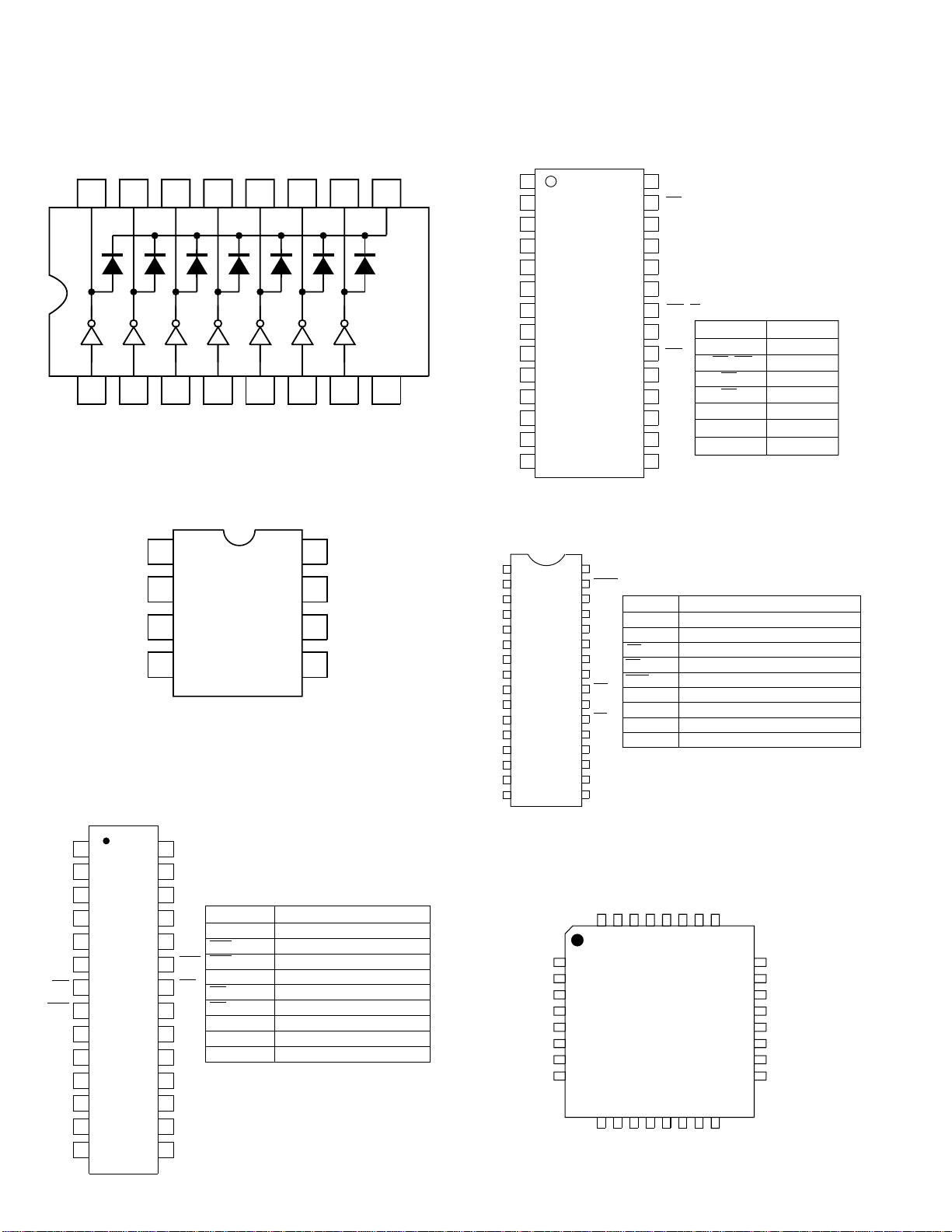
UX-510UA
FO-1470U
[2] IC signal name
CONTROL PWB UNIT
IC1: VHiTD62001AP1 (TD62001AP)
O1 O2 O3 O4 O5 O6 O7 COM
16 15 14 13 12 11 10 9
12345678
I1 I2 I3 I4 I5 I6 I7 GND
IC8: VHiW24258S7LE (W24258S-70LE)
(TOP VIEW)
1
A14
A12
A7
A6
A5
A4
A3
A2
A1
A0
IO1
IO2
IO3
VSS
2
3
4
5
6
7
8
9
10
11
12
13
14
28
VDD
27
WE
26
A13
25
A8
24
A9
23
A11
22
CS2/OE
21
A10
20
CS1
19
IO8
18
IO7
17
IO6
IO5
16
15 IO4
Pin name
A0~A14
CS1/CS2
I/O1~I/O8
WE
OE
VDD
VSS
Signal
Address input
Chip enable
Write enable
Write enable
Data I/O
Power source
Ground
IC15: VHiNJM2113M-1 (NJM2113M)
CD
FC2
FC1
VIN
1
2
3
4
(TOP VIEW)
IC5: RH-iX2168SCZZ (MSM51V4800E)
VCC
DQ1
DQ2
DQ3
DQ4
NC
WE
RAS
A9R
A0
A1
A2
A3
VCC
1
2
3
4
5
6
7
8
9
10
11
12
13
14
VSS
28
DQ8
27
DQ7
26
25
24
23
22
21
20
19
18
17
16
15
DQ5
CAS
OE
NC
A8
A7
A6
A5
A4
VSS
A0~A8, A9R
RAS
CAS
DQ1~DQ8
OE
WE
VCC
VSS
NC
PIN NAME
DQ6
SIGNAL
ADDRESS INPUT
ROW ADDRESS STROBE
COLUMN ADDRESS STROBE
DATA INPUT/OUTPUT
OUTPUT ENABLE
WRITE ENABLE
POWER SUPPLY (+3.3V)
GROUND
NO INTERNAL CONNECTION
8
VO2
7
GND
6
VCC
5 VO1
IC4: VHi27L20012MX (27L2000)
VPP
A16
A15
A12
A7
A6
A5
A4
A3
A2
A1
A0
Q0
Q1
Q2
GND
1
2
3
4
5
6
7
8
9
10
11
12
13
14
15
16
VCC
32
PGM
31
A17
30
29
28
27
26
25
24
23
22
21
20
19
18
17
PIN NAME SIGNAL
A14
A0~A17
A13
Q0~Q7
A8
CE
A9
OE
A11
PGM
OE
VPP
A10
NC
CE
VCC
Q7
GND
Q6
Q5
Q4
Q3
IC13: VHiSCE114//-1 (20415)
MCLK
NC
NC
29
30
12
11
MICBIAS
MICIN–
NC
28
13
VREF
CTRLSIN
Reserved
Reserved
SOUT
SIN
FSYNC
POR
AVSS
NC
31
32
1
2
3
4
5
6
7
8
10
9
MICIN+
LINEIN
ADDRESS INPUT
DATA INPUT/OUTPUT
CHIP ENABLE INPUT
OUTPUT ENABLE INPUT
PROGRAMMABLE ENABLE INPUT
PROGRAM SUPPLY VOLTAGE
NO INTERNAL CONNECTION
POWER SUPPLY PIN (+5V)
GROUND PIN
ICLK
NC
NC
25
26
27
24
MODE0
23
MODE1
22
Reserved
21
DVDD
20
DVSS
19
SPKRO–
18
SPKRO+
17
LINEO
16
15
14
AVSS
AVDD
AGND
8 – 4
Page 85

IC9: VHiSCE114//-1 (SCE114)
UX-510UA
FO-1470U
VSS
D[3]
D[2]
D[1]
D[0]
A[23]/EYEXY
A[22]/EYESYNC
A[21]/EYECLK
A[20]
A[19]
A[18]
VDD
A[17]
A[16]
A[15]
A[14]
VSS
A[13]
A[12]
A[11]
A[10]
A[9]
A[8]
A[7]
A[6]
A[5]
A[4]
VDD
A[3]
A[2]
A[1]
GPIO[20]/ALTTONE
GPIO[19]/RDY/SEROUT
GPIO[11]/BE/SERINP
A[0]
VSS
PCLK/DMAACK
PDAT
PLAT
REGDMA/GPO[18]
WAITN/GPO[19]
SM[2]/GPO[6]
SM[1]/GPO[5]
SM[0]/GPO[4]
VDDPLL
D[4]
D[5]
D[6]
D[7]
167
168
169
170
171
172
173
174
175
176
1
2
3
4
5
6
7
8
9
10
11
12
13
14
15
16
17
18
19
20
21
22
23
24
25
26
27
28
29
30
31
32
33
34
NC
35
NC
36
NC
NC
37
NC
38
39
40
41
42
43
44
54
53
52
51
50
49
48
47
46
45
PM[2]/GPO[2]
PM[1]/GPO[1]
PM[0]/GPO[0]
SM[3]/GPO[7]
163
164
165
166
58
57
56
55
PM[3]/GPO[3]
SXOUT
VDD
160
161
162
61
60
59
SXIN
159
62
VSS
158
63
SYNC/GPO[20]
CS1N/GPO[21]
ROMCSN
WRN
154
155
156
157
67
66
65
64
DEBUGN
RDN
153
68
152
69
TSTCLK
VSSPLL
150
151
71
70
SA1CLK
SR1IO
148
149
73
72
SR3IN/DSPIRQN
SR4OUT
IA1CLK
145
146
147
76
75
74
GPO[31]/SR3OUT
GPIO[37]/IRQ15N
IACLK/DSPCSN
144
IARESET
143
78
77
142
79
141
80
GPIO[0]/SR4IN
140
81
GPIO[36]
VDD
139
82
138
83
GPIO[34]
GPIO[35]
137
136
85
84
GPIO[32]
GPIO[33]
135
134
87
86
GPIO[31]
133
132
131
130
129
128
127
126
125
124
123
122
121
120
119
118
117
116
115
114
113
112
111
110
109
108
107
106
105
104
103
102
101
100
99
98
97
96
95
94
93
92
91
90
89
88
GPIO[30]
GPIO[29]
GPO[30]
GPO[29]
GPO[28]
GPO[27]
GPO[26]
GPIO[28]
GPIO[27]
GPIO[26]
GPIO[25]
VSS
TONE
VDD
START
CLK1
CLK1N/GPO[25]
CLK2/GPO[24]
FCSN[1]/VIDCTL[0]/GPO[23]
FCSN[2]/VIDCTL[1]/GPO[22]
PGIO[8]/FWRN
PGIO[9]/FRDN
PGIO[1]/SASTXD
PGIO[2]/SASRXD
PGIO[3]/SASCLK
PGIO[18]/IRQ[9]N
VSS
RESETN
OPI[0]/GPIO[21]/SSRXD1
OPI[1]/GPIO[22]/SSSTAT1
OPI[2]/GPIO[23]/SSCLK1
OPI[3]/GPIO[24]
OPO[0]/GPO[8]/SMPWRCTRL
OPO[1]/GPO[9]/PMPWRCTRL
OPO[2]/GPO[10]/RINGER
OPO[3]/GPO[11]
OPO[4]/GPO[12]/SSTXD1
OPO[5]/GPO[13]
OPO[6]/GPO[14]
OPO[7]/GPO[15]
THADI
VDD
VREFP
VREFN
STRB[2]
STRB[3]
VDD
STRBPOL/DMAREQ
STRB[0]
STRB[1]
GPIO[14]/CS[4]N
GPIO[15]/CS[5]N
GPIO[16]/IRQ[8]
GPIO[17]
LEDCTRL/GPO[16]
VSS
GPIO[4]/CPCIN
GPIO[12]/CS[2]N
GPIO[13]/CS[3]N
GPIO[6]/SSTXD2
GPIO[7]/SSRXD2
LCDCS/GPO[17]
NC
CAS[1]N
RASN
VDRAM
GPIO[10]/SSSTAT2
GPIO[5]/SSCLK2
8 – 5
DWRN
CAS[0]N
VBAT
XIN
WRPROTN
XOUT
CS0N
TEST[0]
TEST[1]
NC
PWRDWNN
INTPWRDWNEN
BATRSTN
VIN
VREFN/CLREF
ADGA
ADGA
ADVA
ADXG
VREFP
Page 86
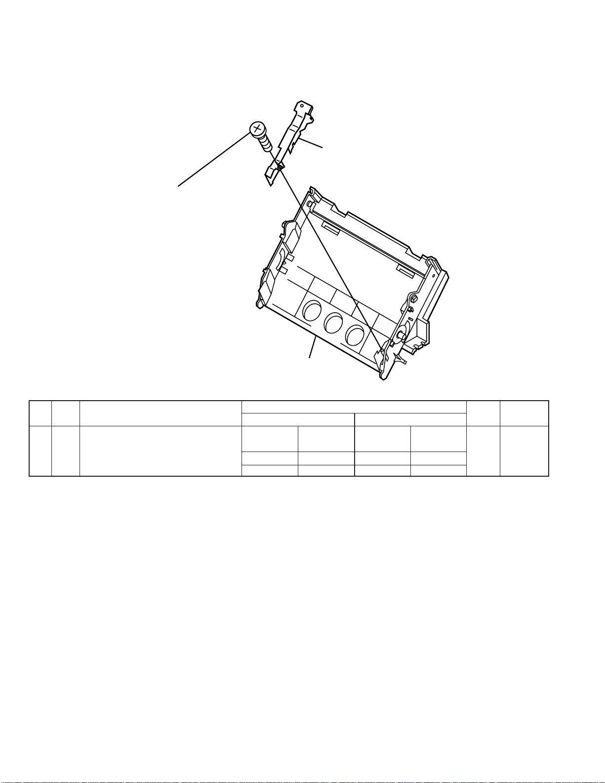
UX-510UA
FO-1470U
[3] Changing the record paper size
How to change the A4 size and letter size of the record papers
1) It becomes the record paper of the A4 size by installing A4 paper guide (PGiDM2493XHSA)
which shows in the drawing. Remove A4 guide when you use the record paper of the letter size.
A4 paper guide
PGiDM2493XHSA
Screw
XEBSD30P10000
RP hopper
2) Set soft switch SW-L2 No.1 and the initialization of SW-L2 No.2 as follows.
SW
DA TA
NO.
NO.
SW
l
L2
Paper set size LETTER LEGAL A4 OPTION
1No. 10010
2No. 20100
ITEM
Switch setting and function
1
Initial
0
setting
Remarks
8 – 6
Page 87
PARTS GUIDE
MODEL FO-1470
SELECTION CODE DESTINATION
U U.S.A.
UX-510UA
FO-1470U
UX-510A
1 Cabinet, etc.
2 Upper cabinet
3 Document guide upper
4 Optical unit
5 Drive unit
6 Head unit
CONTENTS
7 Packing material & Accessories
8 Control PWB unit
9 TEL/LIU PWB unit
10 Power supply PWB unit
11 Operation panel PWB unit
Index
Because parts marked with " " are indispensable for the machine safety maintenance and operation, it must be
replaced with the parts specific to the product specification.
Page 88
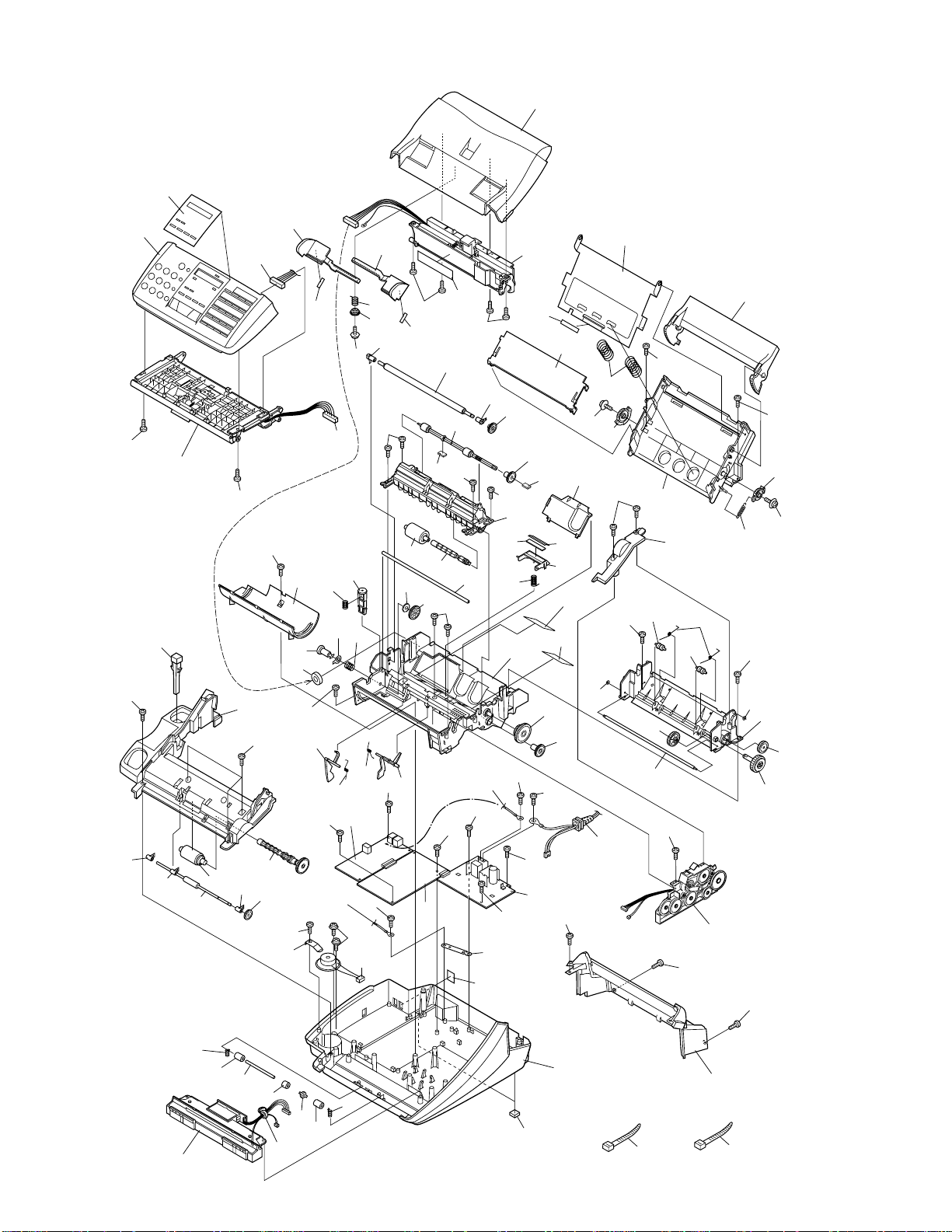
UX-510UA
FO-1470U
[1] Cabinet, etc.
22
99
1
B2
DOCUMENT
GUIDE
UPPER
8
B2
25
HEAD
UNIT
74
72
B7
26
23
24
53
81
B2
27
B2
58
2
81
66
67
B11
68
53
B2
2
46
54
B3
70
B11
50
B2
B2
76
31
14
37
29
34
35
45
41
39
95
51
B2
40
B2
43
36
52
28
90
42
30
86
87
77
B11
B2
63
73
78
60
63
71
B3
69
B2
B2
7
7
OPTICAL UNIT
17
11
18
10
19
12
7
B2
94
W1
B2
57
62
33
TEL/LIU
ARG
CABLE
B2
B4
B2
B2
38
38
32
B2
5
6
HEAD
EARTH
9
CABLE
B2
98
B3
B2
3
4
B2
97
B2
21
B5
55
B11
20
64
B2
B10
W2
65
61
59
DRIVE
UNIT
80
B10
15
75
17
93
18
14
79
13
100mm
84
(BLACK)
– 1 –
Page 89
UX-510UA
FO-1470U
NO.
PARTS CODE
PRICE
RANK
NEW
MARK
PART
RANK
DESCRIPTION
[1] Cabinet,etc.
1 DCEKP264CXH01 BH N E Operation panel unit [510UA]
DCEKP264CXH02 AT N E Operation panel unit [1470U]
2 QCNW-390AXHZZ AK N C Panel cable
3 CCNW-391AXH01 AK N C Speaker ass’y
4 DCEKC281PXHZZ BU N E Control PWB unit(Within ROM)
5 DCEKL266CXH01 BC N E TEL/LIU PWB unit
6 CGERH2363AX01 AK C Feed gear ass’y
7 LBSHP2088AXZZ AC C Transfer bearing
8 MLEVP2253XHYA AD N C Hook switch lever
9 NGERH2275XHZZ AC C Transfer gear 2
10 NROLR2333XHZZ AP C Paper feed roller
11 NROLR2467XHZZ AM N C Transfer roller
12 PGIDM2481XHYA AP N C Document guide lower [510UA]
PGIDM2481XHYB AG N C Document guide lower [1470U]
13 LBNDJ2006XHZZ AA C Band(100mm)
14 RCORF2125XHZZ AE B Core(TRA31)
!
15 GCABB2290XHAA AZ N D Lower cabinet [510UA]
GCABB2290XHAB AL N D Lower cabinet [1470U]
17 MSPRC3039XHFJ AC C Pinch roller spring 2
18 NROLP2334XHZA AC C Pinch roller
19 NSFTZ2281XHZZ AD C Pinch roller shaft
20 QACCD2054XHZZ AP N B AC cord
!
21 RDENT2157XHZZ BF N E Power supply PWB unit
!
22 GCOVA2376XHYA AP N C Top cover [510UA]
GCOVA2376XHYB AG N C Top cover [1470U]
23 MSPRC3249XHZZ AB N C Hopper spring
24 NGERP2318XHZZ AD C Pinion gear
25 PGIDM2483XHYA AE N C Hopper guide,left [510UA]
PGIDM2483XHYB AC N C Hopper guide,left [1470U]
26 PGIDM2484XHYA AE N C Hopper guide,right [510UA]
PGIDM2484XHYB AC N C Hopper guide,right [1470U]
27 TLABH4161AXZZ AD D Imaging film set label
28 LFRM-2180XHAZ AX N C Main frame
29 LPLTM2791AXFW AD C Hold down plate B
30 LPLTP2884AXZZ AP C Separate plate
31 LSTPP2044XHZZ AF C Back tention stopper
32 MLEVP2249XHYZ AD N C P-IN sensor lever
33 MLEVP2252XHYZ AD N C Film sensor lever
34 MLEVP2258XHYZ AD N C Cover switch lever
35 MSPRC2999XHFJ AC C Back tention spring
36 MSPRC3247XHZZ AB N C Separate plate spring
37 MSPRC2927AXFJ AC C Pop up spring
38 MSPRD2929AXFJ AC C Sensor lever spring
39 NGERH2310XHZZ AE C Back tension gear
40 NSFTM2280AXZZ AK C Film guide shaft B
41 PFLT-2009AXZZ AD C Back tension felt
42 PSHEZ3344AXZZ AD C Separate sheet
43 PSHEZ3293AXZZ AH C Separate plate sheet
45 CROLR2362AX01 AN C PU roller ass’y
46 CROLR2363XH02 AK N C PO roller ass’y
50 NGERH2359AXZZ AD C PO gear
51 NSFTM2268XHYZ AE N C PU roller shaft
52 PGIDM2479XHYA AK N C U turn guide
53 LBSHP2086AXZZ AC C Platen bearing
54 NGERH2309XHZZ AC C Platen gear
55 NGERH2358AXZZ AC C PU gear
57 NGERH2361AXZZ AE C Reduction gear A
58 NROLR2468XHZZ AS N C Platen roller
59 CGERH2314AX51 AP C Slip gear ass’y
60 MSPRD3250XHZZ AB N C PO pinch roller spring
61 NGERH2279XHZZ AC C Idler gear A
62 NGERH2367AXZZ AD C Take-up gear
63 NROLP2332XHZZ AD C PO pinch roller
64 NSFTM2279AXZZ AK C Film shaft C
65 PGIDM2485XHYA AC N C PO guide
66 LPLTM2924XHFW AQ C Paper up plate
67 LPLTP2888XHYA AG N C RP release plate [510UA]
LPLTP2888XHYB AC N C RP release plate [1470U]
68 MSPRC2926AXFJ AD C Cassette spring
69 MSPRT2932AXFJ AC C RP release spring
70 NGERH2365AXZZ AD C RP release gear,left
71 NGERH2366AXZZ AD C RP release gear,right
72 PGIDM2480XHYA AF N C Paper guide
73 PHOP-2095XHYA AM N C RP hopper [510UA]
PHOP-2095XHYB AE N C RP hopper [1470U]
74 PSEL-2015SCZZ AB C RP pad
75 GCABC2291XHYA AH N D Rear cabinet [510UA]
GCABC2291XHYB AL N D Rear cabinet [1470U]
76 GCOVA2375XHYZ AK N C ROM cover
77 GCOVA2378AXZZ AE C Memory cover
– 2 –
Page 90
UX-510UA
FO-1470U
NO.
PARTS CODE
PRICE
RANK
NEW
MARK
PART
RANK
DESCRIPTION
[1] Cabinet,etc.
78 PCOVA2114XHYZ AE N C Side cover
79 GLEGG2063AXZZ AC C Rubber leg
80 PSHEZ3563XHZZ AB N C Jack sheet
81 PSHEZ3332AXZZ AE C Hopper sheet
84 LBNDJ2008SCZZ AA C Band(Black)
86 PSHEZ3341AXZZ AC C Guide sheet, left
87 PSHEZ3342AXZZ AC Guide sheet, right
90 PCUSG2112XHZZ AE C PO gear cushion
93 LPLTP2968XHZZ AP C Document kick plate
94 NROLP2396XHZZ AD C Document kick roller
95 PCUSS2114XHZZ AD C PO cushion
97 LPLTM3122XHZZ AD N C Earth plate
98 MSPRP3123XHZZ AC C Speaker holder spring
99 HPNLH2405XHSA AG N D Decoration panel [510UA]
HPNLH2405XHSB AC N D Decoration panel [1470U]
B2 XEBSD30P10000 AA C Screw(3x10)
B3 LX-BZ2222AXZZ AC C Screw
B4 XBPSD30P06K00 AA C Screw(3x6)
B5 XBPSN40P06K00 AA C Screw(4x6)
B7 LX-BZ2138XHZZ AB C Screw(3x6)
B10 XEBSE30P10000 AA C Screw(3x10)
B11 XEBSF30P12000 AA C Screw(3x12)
W1 LX-WZ2228XHZZ AB C Cut washer
W2 LX-WZ2246XHZZ AB C Washer
– 3 –
Page 91
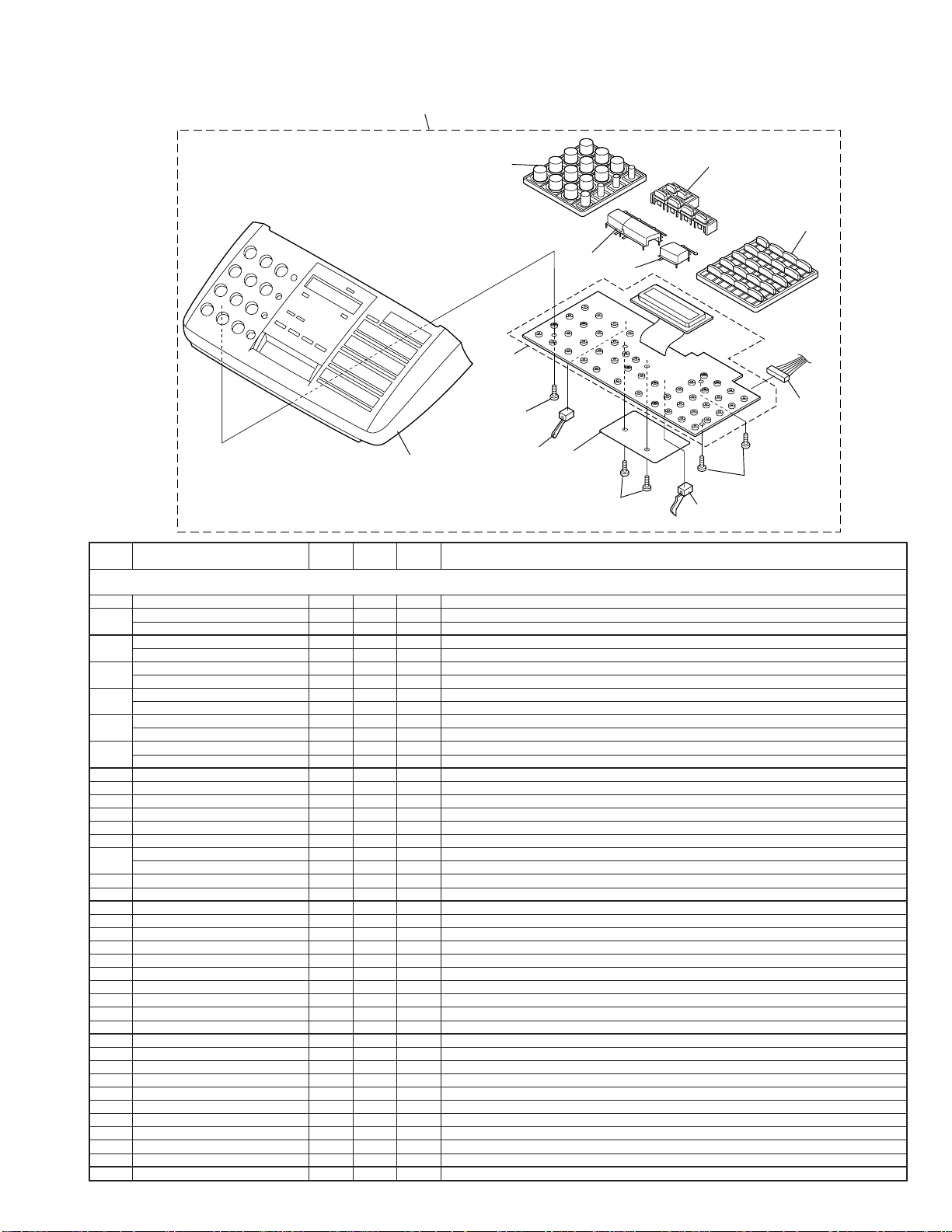
[2] Upper cabinet
UX-510UA
FO-1470U
901
3
7
4
5
6
1
B1
9
2
8
B1
NO.
PARTS CODE
PRICE
RANK
NEW
MARK
PART
RANK
B1
DESCRIPTION
10
[2] Upper cabinet
1 DCEKP351BXH02 BF N E Operation panel PWB unit(Without sensor)
2 GCABA2289XHYA AR N D Upper cabinet [510UA]
GCABA2289XHYB AE N D Upper cabinet [1470U]
3 JBTN-2202XHYA AH N C 12 key [510UA]
JBTN-2202AXSC AG C 12 key [1470U]
4 JBTN-2203XHYA AF N C Direct key [510UA]
JBTN-2203AXSC AF C Direct key [1470U]
5 JBTN-2204XHYA AE N C Start key [510UA]
JBTN-2204AXSB AD C Start key [1470U]
6 JBTN-2205XHYA AD N C Stop key [510UA]
JBTN-2205AXSB AD C Stop key [1470U]
7 JBTN-2206XHYA AE N C Mode key [510UA]
JBTN-2206XHYB AC N C Mode key [1470U]
8 PSHEZ3291AXZZ AD C Insulation sheet
9 QSW-M2246AXZZ AH C FRSNS sensor [FRSNS]
10 QSW-M2247AXZA AE C ORGSNS sensor [ORGNSN]
11 QCNW-390AXHZZ AK N C Panel cable
B1 XEBSD20P06000 AA C Screw(2x6)
901 DCEKP264CXH01 BH N E Operation panel unit [510UA]
DCEKP264CXH02 AT N E Operation panel unit [1470U]
(Unit)
11
– 4 –
Page 92
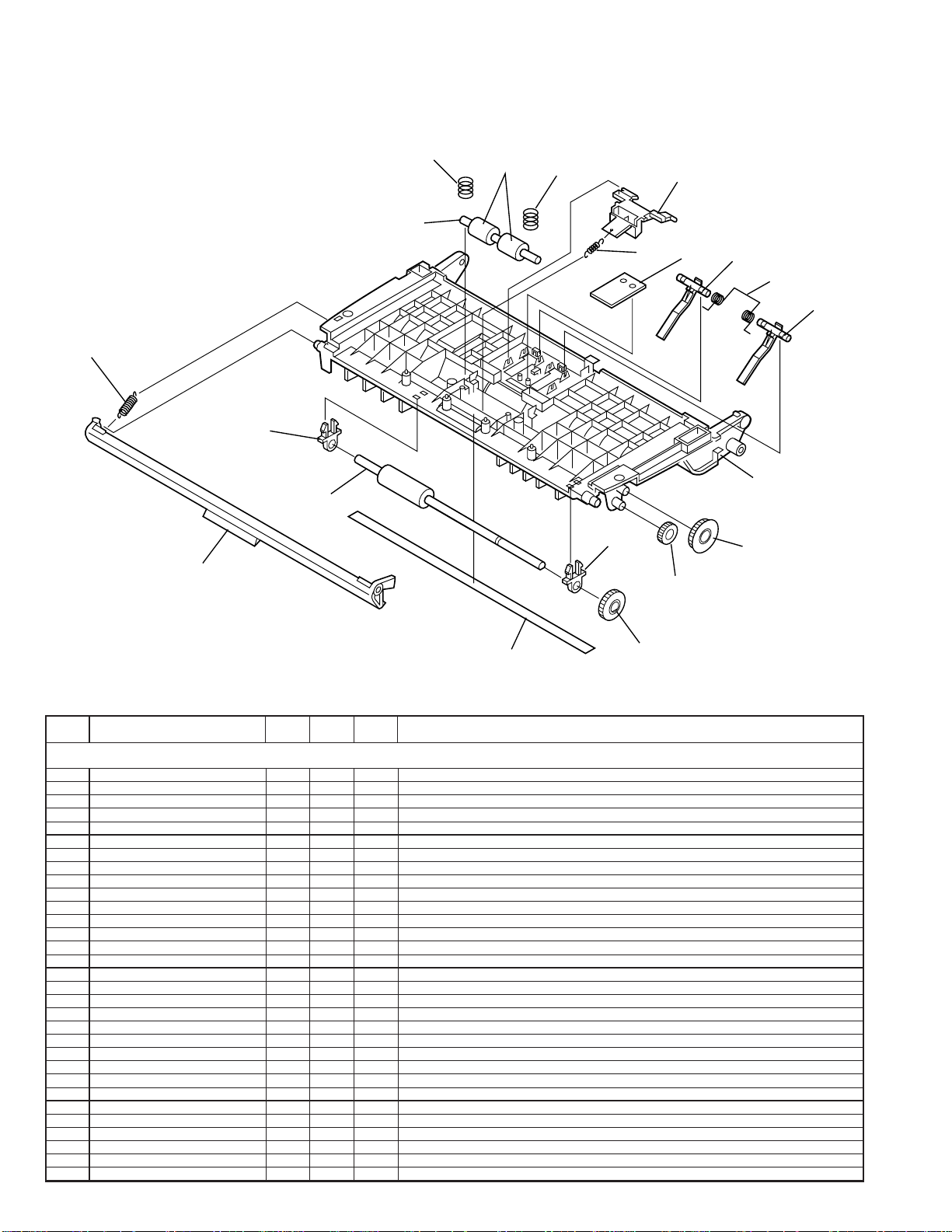
UX-510UA
FO-1470U
[3] Document guide upper
6
3
8
13
14
4
12
4
8
7
2
11
1
17
5
17
15
10
NO.
[3] Document guide upper
1 LPLTG2707XHZZ AE C Separation rubber
2 LPLTP2790XHZZ AD C Separate plate
3 MLEVP2257XHZA AC N C Panel lock lever
4 MSPRC2924AXFJ AC C Pinch roller spring
5 MSPRD3197XHZZ AD N C Paper feed spring
6 MSPRT2923AXFJ AC C Panel lock lever spring
7 MSPRT3235XHZZ AB N C Separate spring
8 NBRGP2141AXZZ AC C Transfer bearing
9 NGERH2275XHZZ AC C Transfer gear 2
10 NGERH2317XHZZ AC C Idler gear,28Z
11 NGERH2356XHZZ AC C Idler gear,20Z
12 NROLP2334XHZA AC C Pinch roller
13 NROLR2466XHZZ AK N C Transfer roller
14 NSFTZ2257AXZZ AE C Pinch roller shaft
15 PGIDM2482XHAZ AM N C Document guide upper
16 PSHEZ3290AXZZ AD C Rear sheet
17 MARMP2026XHZZ AC N C Paper feed arm
PARTS CODE
PRICE
RANK
NEW
MARK
PART
RANK
16
9
DESCRIPTION
– 5 –
Page 93
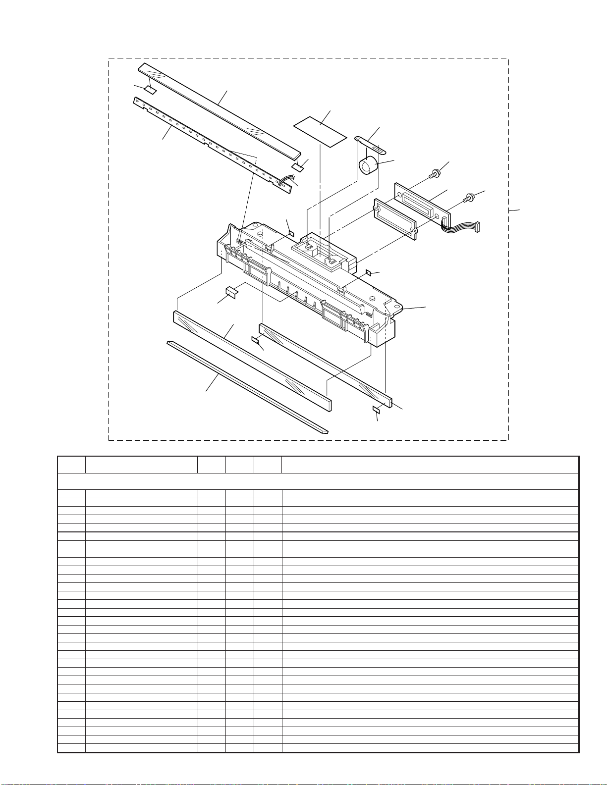
[4] Optical unit
UX-510UA
FO-1470U
12
14
5
10
3
15
13
12
6
B8
1
B8
901
15
4
2
9
17
7
NO.
[4] Optical unit
1 DCEKD475AAX05 BE E CCD PWB unit
2 LFRM-2164XHAA AF N C Optical frame
3 MSPRP2817SCZZ AC C Lens holding spring
4 PFLT-2006XHZZ AA C Felt
5 PGLSP2058XHZZ AE C Reader glass
6 PLNS-2049XHZZ AZ C Lens
7 PMIR-2070XHZZ AG C Mirror 1
8 PMIR-2071XHZZ AH C Mirror 2
9 PMIR-2072XHZZ AH C Mirror 3
10 PSHEZ3196AXZZ AC C Shading sheet
12 PSHEZ3258AXZZ AD C Shading sheet 3
13 QCNW-395AXHZZ AD N C LED cable
14 VHPSNK15A24-1 AZ B LED
15 PCUSS2124XHZZ AA N C Cushion,optical frame
17 PSHEP3606XHZZ AA N C Mirror sheet 2
B8 LX-BZ2182SCZZ AB C Screw
901 DCYOD475AXH03 BN N E Optical unit
PARTS CODE
(Unit)
PRICE
RANK
NEW
MARK
PART
RANK
8
17
DESCRIPTION
– 6 –
Page 94
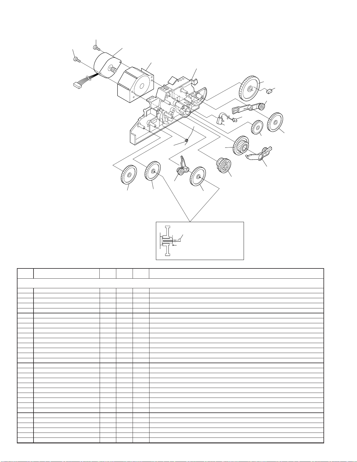
UX-510UA
FO-1470U
[5] Drive unit
B2
B2
14
11
5
11
4
15
16
3
12
13
8
7
10
9
2
1
6
9
NO.
PARTS CODE
PRICE
RANK
NEW
MARK
PART
RANK
[5] Drive unit
1 CLEVP2254AX01 AE C Planet lever A ass’y
2 CLEVP2255AX01 AE C Planet lever B ass’y
3 CLEVP2256AX01 AE C Planet lever C ass’y
4 LFRM-2181AXZZ AV C Drive unit frame
5 LPLTM2886AXFW AQ C Motor heat sink
6 MCAMP2023AXZZ AD C Cam A
7 MSPRD2962AXFJ AC C Cam hold spring
8 NGERH2279XHZZ AC C Idler gear A
9 NGERH2281XHZZ AD C Idler gear C
10 NGERH2361AXZZ AE C Reduction gear A
11 NGERH2362AXZZ AE C Reduction gear C
12 QCNW-394AXHZZ AD N C Cam switch cable
13 QSW-F2224SCZZ AE C Cam switch
14 RMOTZ2161XHZZ AX N B Motor
15 NGERH2360AXZZ AE C Reduction gear B
16 PCUSG2111XHZZ AE C Cushion
17 LBNDJ2006XHZZ AA C Band
B2 XEBSD30P10000 AA C Screw(3x10)
17
Cut after insert must be
touch to the bottom.
DESCRIPTION
– 7 –
Page 95
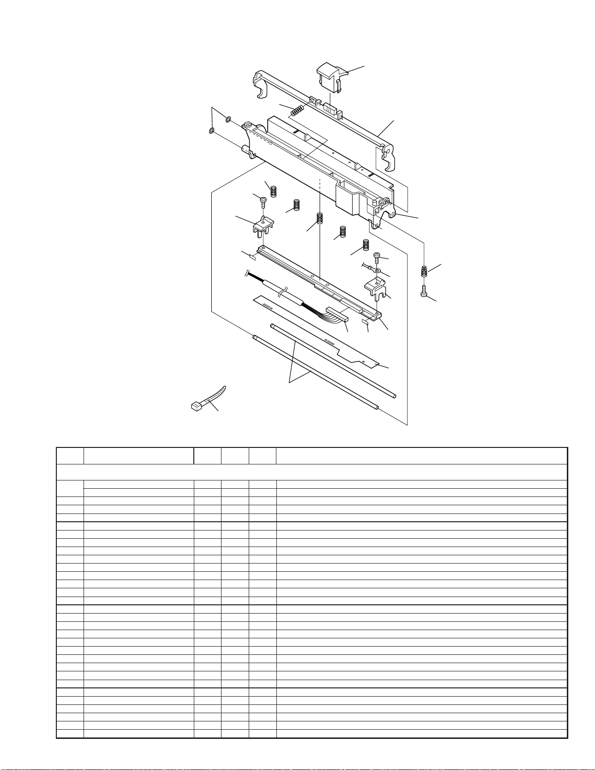
[6] Head unit
UX-510UA
FO-1470U
1
W1
6
16
B6
95
15
17
4
3
5
16
B6
7
13
B2
12
17
10
14
11
8
2 (100mm)
NO.
[6] Head unit
1 JKNBP2074XHYA AD N C Release knob [510UA]
2 LBNDJ2006XHZZ AA C Band(100mm)
3 LFRM-2179XHZA AK N C Head frame
4 MLEVP2248AXZZ AD C Lock lever
5 MSPRC2964AXFJ AD C Head spring B
6 MSPRC2920AXFJ AC C Lock spring
7 MSPRC2928AXFJ AC C Pop up spring
8 NSFTM2278AXZZ AH C Film guide shaft
9 PGIDM2519XHZL AN C Head guide,left
10 PGIDM2478AXZR AD C Head guide,right
11 PSHEZ3292AXZZ AE C Head guide sheet
12 QCNW-392AXHZZ AM N C Head cable
13 QCNW-393AXHZZ AE N C Head earth cable
14 RHEDZ2063XHZZ BQ N B Termal head
15 MSPRC3210XHZZ AE N C Head spring 1
16 MSPRC3212XHZZ AD N C Head spring 2
17 PSHEZ3366XHZZ AD C Head sheet
B2 XEBSD30P10000 AA C Screw(3x10)
B6 XBBSD30P06000 AA C Screw(3x6)
W1 LX-WZ2228AXZZ AB C Cut washer
PARTS CODE
JKNBP2074XHYB AC N C Release knob [1470U]
PRICE
RANK
NEW
MARK
PART
RANK
DESCRIPTION
– 8 –
Page 96
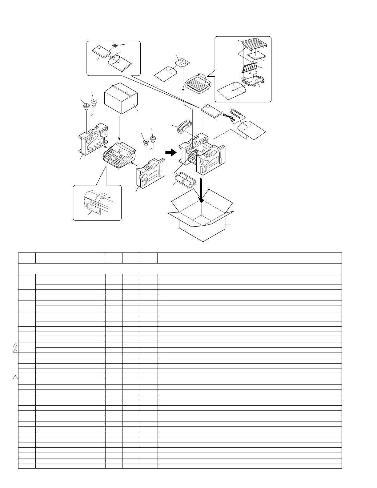
UX-510UA
FO-1470U
[7] Packing material & Accessories
17
13
11
12
15
TAPE
10
4
TAPE
5
3
2
7
TAPE
1
6
Turn
Over
16
13
13
9
14
TAPE
18
19
NO.
PARTS CODE
PRICE
RANK
NEW
MARK
PART
RANK
DESCRIPTION
[7] Packing material & Accessories
1 TCADZ3055XHZZ AN N D Pop card
2 LPLTP2889XHYA AM N C Paper tray A [510UA]
LPLTP2889XHYB AE N C Paper tray A [1470U]
3 LPLTP2890XHYA AM N C Paper tray B [510UA]
LPLTP2890XHYB AE N C Paper tray B [1470U]
4 PCOVA2115XHSB AE N C Paper tray cover [510UA]
PCOVA2115XHSA AL C Paper tray cover [1470U]
5 SPAKA328CXHZZ AC N D Protection pad,paper tray
6 TINSE4157XHTZ AK N D Operation manual [510UA]
TINSE4162XHTZ AL N D Operation manual [1470U]
7 TLABH276CXHZZ AD N D Rapid key labels
9 DUNTK464BXHFW AX N E Handset [510UA]
DUNTK464BXHOG AP E Handset [1470U]
10 QCNW-289ASCOW AG C Handset cord [510UA]
!
!
!
QCNW-289ASCOG AG C Handset cord [1470U]
11 SPAKA213AAXZZ AC D Protection sheet
12 LBSHP2078XHZZ AC C Imaging film frange
13 NGERH2315XHZZ AE C Imaging film gear
14 PRBNN2009SCZZ AV S Imaging film(Initial starter film 20m)
15 QCNW-290ASCZZ AE C Telephone line cord
16 SPAKP4381AXZZ AG D Vinyl cover
17 SPAKA261CXHZZ AC N D Packing add.,left
18 SPAKA262CXHZZ AC N D Packing add.,right
19 SPAKC263CXHZZ AG N D Packing case [510UA]
SPAKC300CXHTZ AK N D Packing case [1470U]
– 9 –
Page 97
UX-510UA
FO-1470U
NO.
PARTS CODE
PRICE
RANK
NEW
MARK
PART
RANK
DESCRIPTION
[8] Control PWB unit
1 UBATL2049SCZZ AF B Battery(CR2032T23) [BAT1]
2 VCEAGA1EW476M AA C Capacitor(25WV 47µF) [C1]
3 VCEAGA1HW226M AB C Capacitor(50WV 22µF) [C2]
4 VCEAGA1HW106M AA C Capacitor(50WV 10µF) [C3]
5 VCEAGA1HW107M AA C Capacitor(50WV 100µF) [C4]
6 VCEAGA0JW227M AD C Capacitor(6.3WV 220µF) [C5]
7 VCEAGA0JW227M AD C Capacitor(6.3WV 220µF) [C6]
8 VCEAGA1HW107M AA C Capacitor(50WV 100µF) [C7]
9 VCEAGA1HW226M AB C Capacitor(50WV 22µF) [C8]
10 VCEAGA1EW476M AA C Capacitor(25WV 47µF) [C11]
11 VCEAGA1HW106M AA C Capacitor(50WV 10µF) [C12]
12 VCEAGA1HW107M AA C Capacitor(50WV 100µF) [C13]
13 VCEAGA1HW106M AA C Capacitor(50WV 10µF) [C14]
14 VCEAGA1HW106M AA C Capacitor(50WV 10µF) [C15]
15 VCKYCY1EF104Z AA C Capacitor(25WV 0.1µF) [C100]
16 VCKYCY1AF105Z AC C Capacitor(10WV 1µF) [C101]
17 VCKYCY1AF105Z AC C Capacitor(10WV 1µF) [C102]
18 VCKYTV1HF104Z AA C Capacitor(50WV 0.1µF) [C104]
19 VCCCCY1HH101J AA C Capacitor(50WV 100PF) [C105]
20 VCCCCY1HH101J AA C Capacitor(50WV 100PF) [C107]
21 VCKYCY1HB102K AA C Capacitor(50WV 1000PF) [C109]
22 VCKYCY1HB102K AA C Capacitor(50WV 1000PF) [C110]
23 VCKYCY1AF105Z AC C Capacitor(10WV 1µF) [C111]
24 VCKYCY1HB102K AA C Capacitor(50WV 1000PF) [C112]
25 VCKYCY1HB102K AA C Capacitor(50WV 1000PF) [C113]
26 VCKYTV1CF225Z AD C Capacitor(16WV 2.2µF) [C114]
27 VCCCCY1HH180J AA C Capacitor(50WV 18PF) [C115]
28 VCCCCY1HH330J AA C Capacitor(50WV 33PF) [C116]
29 VCKYCY1AF105Z AC C Capacitor(10WV 1µF) [C117]
30 VCKYCY1AF105Z AC C Capacitor(10WV 1µF) [C118]
31 VCKYTV1HF104Z AA C Capacitor(50WV 0.1µF) [C125]
32 VCKYCY1EF104Z AA C Capacitor(25WV 0.1µF) [C126]
33 VCKYCY1AF105Z AC C Capacitor(10WV 1µF) [C127]
34 VCKYCY1AF105Z AC C Capacitor(10WV 1µF) [C128]
35 VCKYCY1EF104Z AA C Capacitor(25WV 0.1µF) [C129]
36 VCKYCY1AF105Z AC C Capacitor(10WV 1µF) [C130]
37 VCKYCY1HB102K AA C Capacitor(50WV 1000PF) [C131]
38 VCKYCY1HB102K AA C Capacitor(50WV 1000PF) [C132]
39 VCKYCY1HB102K AA C Capacitor(50WV 1000PF) [C133]
40 VCKYTV1CF225Z AD C Capacitor(16WV 2.2µF) [C134]
41 VCKYCY1EF104Z AA C Capacitor(25WV 0.1µF) [C135]
42 VCKYCY1AF105Z AC C Capacitor(10WV 1µF) [C136]
43 VCKYCY1AF105Z AC C Capacitor(10WV 1µF) [C137]
44 VCKYCY1AF105Z AC C Capacitor(10WV 1µF) [C138]
45 VCKYCY1AF105Z AC C Capacitor(10WV 1µF) [C139]
46 VCKYCY1AF105Z AC C Capacitor(10WV 1µF) [C140]
47 VCKYTV1CF225Z AD C Capacitor(16WV 2.2µF) [C141]
48 VCKYCY1AF105Z AC C Capacitor(10WV 1µF) [C142]
49 VCKYCY1HB102K AA C Capacitor(50WV 1000PF) [C143]
50 VCCCCY1HH101J AA C Capacitor(50WV 100PF) [C144]
51 VCKYTV1CF225Z AD C Capacitor(16WV 2.2µF) [C146]
52 VCKYTV1CF225Z AD C Capacitor(16WV 2.2µF) [C147]
53 VCKYCY1HB102K AA C Capacitor(50WV 1000PF) [C148]
54 VCKYCY1HB102K AA C Capacitor(50WV 1000PF) [C149]
55 VCKYCY1HB102K AA C Capacitor(50WV 1000PF) [C150]
56 VCKYCY1HB102K AA C Capacitor(50WV 1000PF) [C151]
57 VCCCCY1HH101J AA C Capacitor(50WV 100PF) [C152]
58 VCKYCY1EF104Z AA C Capacitor(25WV 0.1µF) [C154]
59 VCKYTV1CF225Z AD C Capacitor(16WV 2.2µF) [C157]
60 VCKYTV1CF225Z AD C Capacitor(16WV 2.2µF) [C158]
61 VCKYTV1CF225Z AD C Capacitor(16WV 2.2µF) [C159]
62 VCKYTV1CF225Z AD C Capacitor(16WV 2.2µF) [C160]
63 VCKYTV1CF225Z AD C Capacitor(16WV 2.2µF) [C161]
64 VCCCCY1HH101J AA C Capacitor(50WV 100PF) [C163]
65 VCCCCY1HH101J AA C Capacitor(50WV 100PF) [C164]
66 VRS-CY1JB000J AA C Resistor(1/16W 0Ω ±5%) [C168]
67 VCKYCY1HB103K AA C Capacitor(50WV 0.01µF) [C169]
68 VCKYCY1HB472K AA C Capacitor(50WV 4700PF) [C170]
69 VCKYCY1AF105Z AC C Capacitor(10WV 1µF) [C171]
70 VCCCCY1HH150J AB C Capacitor(50WV 15PF) [C174]
71 VCCCCY1HH150J AB C Capacitor(50WV 15PF) [C175]
72 VCKYCY1EF104Z AA C Capacitor(25WV 0.1µF) [C176]
73 VCCCCY1HH101J AA C Capacitor(50WV 100PF) [C177]
74 VCCCCY1HH101J AA C Capacitor(50WV 100PF) [C178]
75 VCCCCY1HH101J AA C Capacitor(50WV 100PF) [C179]
76 VCCCCY1HH101J AA C Capacitor(50WV 100PF) [C180]
77 VCKYCY1EF104Z AA C Capacitor(25WV 0.1µF) [C182]
78 VCCCCY1HH150J AB C Capacitor(50WV 15PF) [C183]
79 VCKYTV1HF104Z AA C Capacitor(50WV 0.1µF) [C185]
80 VRS-CY1JB000J AA C Resistor(1/16W 0Ω ±5%) [C186]
– 10 –
Page 98
UX-510UA
FO-1470U
NO.
PARTS CODE
PRICE
RANK
NEW
MARK
PART
RANK
DESCRIPTION
[8] Control PWB unit
81 VCKYCY1CB104K AB C Capacitor(16WV 0.1µF) [C188]
82 VCKYCY1CB104K AB C Capacitor(16WV 0.1µF) [C189]
83 VCKYCY1AF105Z AC C Capacitor(10WV 1µF) [C190]
84 VRS-CY1JB000J AA C Resistor(1/16W 0Ω ±5%) [C191]
85 VCKYCY1AF105Z AC C Capacitor(10WV 1µF) [C192]
86 VRS-CY1JB000J AA C Resistor(1/16W 0Ω ±5%) [C196]
87 VCKYCY1EF104Z AA C Capacitor(25WV 0.1µF) [C197]
88 VCKYCY1CB104K AB C Capacitor(16WV 0.1µF) [C198]
89 VRS-CY1JB000J AA C Resistor(1/16W 0Ω ±5%) [C207]
90 VRS-CY1JB000J AA C Resistor(1/16W 0Ω ±5%) [C214]
91 VCKYCY1AF105Z AC C Capacitor(10WV 1µF) [C216]
92 VCCCCY1HH221J AA C Capacitor(50WV 220PF) [C218]
93 VCKYCY1AF105Z AC C Capacitor(10WV 1µF) [C219]
94 VCKYCY1EF104Z AA C Capacitor(25WV 0.1µF) [C220]
95 VCKYCY1EF104Z AA C Capacitor(25WV 0.1µF) [C221]
96 VCKYCY1AF105Z AC C Capacitor(10WV 1µF) [C223]
97 VCKYCY1HB102K AA C Capacitor(50WV 1000PF) [C224]
98 VCTYPA1HF104Z AC C Capacitor(50WV 0.1µF) [C227]
99 QCNCM7014SC0G AB C Connector(7pin) [CNCCD]
100 QCNCM2442SC0B AB C Connector(2pin) [CNCSW]
101 QCNCM7014SC0B AD C Connector(2pin) [CNLED]
102 QCNCM2499SC1D AG C Connector(14pin) [CNLIUA]
103 QCNCM7014SC0F AB C Connector(6pin) [CNMT]
104 QCNCM7014SC1E AC C Connector(15pin) [CNPN]
105 QCNCM2499SC0F AF C Connector(6pin) [CNPW]
106 QCNCM2401SC0B AA C Connector(2pin) [CNSP]
107 QCNCM7014SC1F AD C Connector(16pin) [CNTH]
108 VHE1N4748A/-1 AC B Diode(1N4748A) [D1]
109 VHD1SS355//-1 AB B Diode(1SS355) [D100]
110 VHD1SS355//-1 AB B Diode(1SS355) [D101]
111 VHDHRW0202B-1 AD B Diode(HRW0202B) [D102]
112 VHD1SS355//-1 AB B Diode(1SS355) [D103]
113 VHD1SS355//-1 AB B Diode(1SS355) [D104]
114 VHD1SS355//-1 AB B Diode(1SS355) [D105]
115 VHD1SS355//-1 AB B Diode(1SS355) [D106]
116 QFS-P2010SCZZ AD B IC protector(KAB2402) [FU100]
117 VHITD62001AP1 AE B IC(TD62001AP) [IC1]
118 RH-IX2202SCZZ AM N B IC(HCT244) [IC2]
119 RH-IX2203SCZZ AH N B IC(LV125A) [IC3]
120 QSOCZ2051SC32 AC C IC socket(32pin) [IC4]
121 VHI27020FPS0B BN N B IC,EPROM(2MB) [IC4]
122 RH-IX2168SCZZ BB B IC(MSM51V4800E) [IC5]
123 VHIW24258S7LE AQ B IC(W24258S-70LE) [IC8]
124 VHISCE114//-1 BG B IC(SCE114) [IC9](Within IC9 and IC13 pair)
125 RH-IX2201SCZZ AG N B IC(HCT04) [IC10]
126 VHINJM318M/-F AF B IC(NJM318M) [IC11]
127 VHISCE114//-1 BG B IC(20415) [IC13](Within IC9 and IC13 pair)
128 VHINJM2113M-1 AG B IC(NJM2113) [IC15]
129 VRS-CY1JB000J AA C Resistor(1/16W 0Ω ±5%) [L101]
130 VRS-CY1JB000J AA C Resistor(1/16W 0Ω ±5%) [L107]
131 VRS-CY1JB000J AA C Resistor(1/16W 0Ω ±5%) [L112]
132 VRS-TS2AD000J AA C Resistor(1/10W 0Ω ±5%) [L116]
133 VRS-CY1JB000J AA C Resistor(1/16W 0Ω ±5%) [L118]
134 VRS-CY1JB000J AA C Resistor(1/16W 0Ω ±5%) [L119]
135 VHPSG206S//-1 AG B Photo transistor(SG206S) [PI1]
136 VHPSG206S//-1 AG B Photo transistor(SG206S) [PI2]
137 VSDTC143ZK/-1 AD B Transistor(DTC143ZK) [Q100]
138 VSDTC143ZK/-1 AD B Transistor(DTC143ZK) [Q102]
139 VSRNC1402//-1 AC B Transistor(RNC1402) [Q104]
140 VSRNC1402//-1 AC B Transistor(RNC1402) [Q105]
141 VRS-RE3AA102J AA C Resistor(1W 1.0KΩ ±5%) [R1]
142 VRS-CY1JB271J AA C Resistor(1/16W 270Ω ±5%) [R101]
143 VRS-CY1JB474J AA C Resistor(1/16W 470KΩ ±5%) [R102]
144 VRS-CY1JB103J AA C Resistor(1/16W 10KΩ ±5%) [R104]
145 VRS-CY1JB000J AA C Resistor(1/16W 0Ω ±5%) [R106]
146 VRS-CY1JB562J AA C Resistor(1/16W 5.6KΩ ±5%) [R107]
147 VRS-CY1JB271J AA C Resistor(1/16W 270Ω ±5%) [R108]
148 VRS-CY1JB271J AA C Resistor(1/16W 270Ω ±5%) [R109]
149 VRS-CY1JB106J AA C Resistor(1/16W 10MΩ ±5%) [R113]
150 VRS-CY1JB223J AA C Resistor(1/16W 22KΩ ±5%) [R115]
151 VRS-CY1JB000J AA C Resistor(1/16W 0Ω ±5%) [R116]
152 VRS-CY1JB000J AA C Resistor(1/16W 0Ω ±5%) [R117]
153 VRS-CY1JB000J AA C Resistor(1/16W 0Ω ±5%) [R119]
154 VRS-CY1JB513J AA C Resistor(1/16W 51KΩ ±5%) [R120]
155 VRS-CY1JB000J AA C Resistor(1/16W 0Ω ±5%) [R123]
156 VRS-CY1JB000J AA C Resistor(1/16W 0Ω ±5%) [R124]
157 VRS-CY1JB103J AA C Resistor(1/16W 10KΩ ±5%) [R125]
158 VRS-CY1JB000J AA C Resistor(1/16W 0Ω ±5%) [R127]
159 VRS-CY1JB271J AA C Resistor(1/16W 270Ω ±5%) [R128]
160 VRS-CY1JB224J AA C Resistor(1/16W 220KΩ ±5%) [R129]
– 11 –
Page 99
UX-510UA
FO-1470U
NO.
PARTS CODE
PRICE
RANK
NEW
MARK
PART
RANK
DESCRIPTION
[8] Control PWB unit
161 VRS-CY1JB271J AA C Resistor(1/16W 270Ω ±5%) [R130]
162 VRS-CY1JB103J AA C Resistor(1/16W 10KΩ ±5%) [R131]
163 VRS-CY1JB000J AA C Resistor(1/16W 0Ω ±5%) [R132]
164 VRS-CY1JB271J AA C Resistor(1/16W 270Ω ±5%) [R133]
165 VRS-CY1JB271J AA C Resistor(1/16W 270Ω ±5%) [R134]
166 VRS-CY1JB271J AA C Resistor(1/16W 270Ω ±5%) [R135]
167 VRS-CY1JB271J AA C Resistor(1/16W 270Ω ±5%) [R136]
168 VRS-CY1JB000J AA C Resistor(1/16W 0Ω ±5%) [R137]
169 VRS-CY1JB223J AA C Resistor(1/16W 22KΩ ±5%) [R139]
170 VRS-CY1JB103J AA C Resistor(1/16W 10KΩ ±5%) [R140]
171 VRS-CY1JB271J AA C Resistor(1/16W 270Ω ±5%) [R141]
172 VRS-CY1JB271J AA C Resistor(1/16W 270Ω ±5%) [R142]
173 VRS-CY1JB271J AA C Resistor(1/16W 270Ω ±5%) [R143]
174 VRS-CY1JB102J AA C Resistor(1/16W 1KΩ ±5%) [R144]
175 VRS-CY1JB471J AA C Resistor(1/16W 470Ω ±5%) [R146]
176 VRS-CY1JB203J AA C Resistor(1/16W 20KΩ ±5%) [R151]
177 VRS-CY1JB271J AA C Resistor(1/16W 270Ω ±5%) [R152]
178 VRS-CY1JB271J AA C Resistor(1/16W 270Ω ±5%) [R153]
179 VRS-CY1JB471J AA C Resistor(1/16W 470Ω ±5%) [R154]
180 VRS-CY1JB471J AA C Resistor(1/16W 470Ω ±5%) [R155]
181 VRS-CY1JB101J AA C Resistor(1/16W 100Ω ±5%) [R160]
182 VRS-CY1JB000J AA C Resistor(1/16W 0Ω ±5%) [R163]
183 VRS-CY1JB104J AA C Resistor(1/16W 100KΩ ±5%) [R164]
184 VRS-CY1JB000J AA C Resistor(1/16W 0Ω ±5%) [R165]
185 VRS-CY1JB102J AA C Resistor(1/16W 1KΩ ±5%) [R166]
186 VRS-CY1JB203J AA C Resistor(1/16W 20KΩ ±5%) [R168]
187 VRS-CY1JB221J AA C Resistor(1/16W 220Ω ±5%) [R170]
188 VRS-CY1JB105J AA C Resistor(1/16W 1MΩ ±5%) [R171]
189 VRS-CY1JB271J AA C Resistor(1/16W 270Ω ±5%) [R172]
190 VRS-CY1JB271J AA C Resistor(1/16W 270Ω ±5%) [R173]
191 VRS-CY1JB102J AA C Resistor(1/16W 1KΩ ±5%) [R175]
192 VRS-CY1JB333J AA C Resistor(1/16W 33KΩ ±5%) [R176]
194 VRS-CY1JB472J AA C Resistor(1/16W 4.7KΩ ±5%) [R178]
195 VRS-CY1JB393J AA C Resistor(1/16W 39KΩ ±5%) [R179]
196 VRS-CY1JB000J AA C Resistor(1/16W 0Ω ±5%) [R180]
197 VRS-CY1JB000J AA C Resistor(1/16W 0Ω ±5%) [R181]
198 VRS-CY1JB472J AA C Resistor(1/16W 4.7KΩ ±5%) [R182]
199 VRS-CY1JB113J AA C Resistor(1/16W 11KΩ ±5%) [R183]
200 VRS-CY1JB104J AA C Resistor(1/16W 100KΩ ±5%) [R184]
201 VCCCCY1HH221J AA C Capacitor(50WV 220PF) [R185]
202 VRS-CY1JB000J AA C Resistor(1/16W 0Ω ±5%) [R188]
203 VRS-CY1JB000J AA C Resistor(1/16W 0Ω ±5%) [R189]
204 VRS-CY1JB104J AA C Resistor(1/16W 100KΩ ±5%) [R190]
205 VRS-CY1JB302J AA C Resistor(1/16W 3KΩ ±5%) [R195]
206 VRS-CY1JB433J AA C Resistor(1/16W 43KΩ ±5%) [R196]
207 VRS-CY1JB000J AA C Resistor(1/16W 0Ω ±5%) [R198]
208 VRS-CY1JB102J AA C Resistor(1/16W 1KΩ ±5%) [R200]
209 VRS-CY1JB222J AA C Resistor(1/16W 2.2KΩ ±5%) [R201]
210 VRS-CY1JB000J AA C Resistor(1/16W 0Ω ±5%) [R202]
211 VRS-CY1JB271J AA C Resistor(1/16W 270Ω ±5%) [R203]
212 VRS-CY1JB271J AA C Resistor(1/16W 270Ω ±5%) [R204]
213 VRS-TS2AD000J AA C Resistor(1/10W 0Ω ±5%) [R205]
214 VRS-CY1JB271J AA C Resistor(1/16W 270Ω ±5%) [R206]
215 VRS-CY1JB000J AA C Resistor(1/16W 0Ω ±5%) [R207]
216 VRS-CY1JB000J AA C Resistor(1/16W 0Ω ±5%) [R208]
217 VCCCCY1HH221J AA C Capacitor(50WV 220PF) [R209]
218 VRS-CY1JB000J AA C Resistor(1/16W 0Ω ±5%) [R210]
219 VRS-CY1JB224J AA C Resistor(1/16W 220KΩ ±5%) [R212]
220 VRS-CY1JB000J AA C Resistor(1/16W 0Ω ±5%) [R213]
221 VRS-CY1JB103J AA C Resistor(1/16W 10KΩ ±5%) [R220]
222 VRS-CY1JB103J AA C Resistor(1/16W 10KΩ ±5%) [R221]
223 VRS-CY1JB103J AA C Resistor(1/16W 10KΩ ±5%) [R222]
224 RR-TZ3018SCZZ AC B Resistor array(470Ωx4) [RA1]
225 RR-TZ3017SCZZ AC B Resistor array(270Ωx4) [RA2]
226 RR-TZ3017SCZZ AC B Resistor array(270Ωx4) [RA3]
227 RR-TZ3017SCZZ AC B Resistor array(270Ωx4) [RA4]
228 RR-TZ3018SCZZ AC B Resistor array(470Ωx4) [RA5]
229 RR-TZ3018SCZZ AC B Resistor array(470Ωx4) [RA6]
230 RR-TZ3017SCZZ AC B Resistor array(270Ωx4) [RA7]
231 RR-TZ3017SCZZ AC B Resistor array(270Ωx4) [RA8]
232 RR-TZ3017SCZZ AC B Resistor array(270Ωx4) [RA9]
233 RR-TZ3017SCZZ AC B Resistor array(270Ωx4) [RA10]
234 RR-TZ3029SCZZ AB B Resistor array(1KΩx4) [RA11]
235 RR-TZ3017SCZZ AC B Resistor array(270Ωx4) [RA12]
236 RR-TZ3017SCZZ AC B Resistor array(270Ωx4) [RA13]
237 RR-TZ3018SCZZ AC B Resistor array(470Ωx4) [RA14]
238 VHI62FP332P-1 AF B IC(XC62FP3302P) [REG1]
239 RRLYD3130SCZZ AN B Relay(OJE-SH-124DM) [RY1]
240 RCRSB0297AFZZ AD B Crystal(32.768kHz) [X1]
241 RCRSQ2157SCZZ AF B Crystal(32.256MHz) [X2]
– 12 –
Page 100
UX-510UA
FO-1470U
NO.
PARTS CODE
PRICE
RANK
NEW
MARK
PART
RANK
DESCRIPTION
[8] Control PWB unit
242 QCNW-4358XH95 AA N C Jumper wire
901 DCEKC281PXHZZ BU N E Control PWB unit(Within ROM)
(Unit)
[9] TEL/LIU PWB unit
1 VHVRA391PV6-1 AE B Varistor(RA-391P-V6-2) [AR1]
2 QCNW-4704XHZZ AD C Cable [ARG]
3 VCEAGA1HW226M AB C Capacitor(50WV 22µF) [C1]
4 VCEAGA1HW226M AB C Capacitor(50WV 22µF) [C2]
5 VCEAGA1HW475M AA C Capacitor(50WV 4.7µF) [C4]
6 VCEAGA1HW226M AB C Capacitor(50WV 22µF) [C5]
7 VCEAGA1HW226M AB C Capacitor(50WV 22µF) [C6]
8 RC-FZ3024SCZZ AG C Capacitor(250WV 0.82µF) [C8]
9 VCEAGA1HW226M AB C Capacitor(50WV 22µF) [C9]
10 VCEAGA1HW106M AA C Capacitor(50WV 10µF) [C10]
11 VCEAGA1HW226M AB C Capacitor(50WV 22µF) [C13]
12 VCKYCY1EF104Z AA C Capacitor(25WV 0.1µF) [C101]
13 VCKYTV1HF104Z AA C Capacitor(50WV 0.1µF) [C102]
14 VCKYCY1AF105Z AC C Capacitor(10WV 1µF) [C106]
15 VCKYCY1EB393K AB C Capacitor(25WV 0.039µF) [C108]
16 VCCCCY1HH330J AA C Capacitor(50WV 33PF) [C109]
17 VCKYTV1HF104Z AA C Capacitor(50WV 0.1µF) [C110]
18 VCKYCY1HB821K AA C Capacitor(50WV 820PF) [C112]
19 VCKYCY1AF105Z AC C Capacitor(10WV 1µF) [C113]
20 VCCCCY1HH330J AA C Capacitor(50WV 33PF) [C114]
21 VCCCCY1HH221J AA C Capacitor(50WV 220PF) [C115]
22 VCKYCY1HB222K AA C Capacitor(50WV 2200PF) [C117]
23 VCKYTV1HF104Z AA C Capacitor(50WV 0.1µF) [C118]
24 VCKYCY1HB102K AA C Capacitor(50WV 1000PF) [C119]
25 VCKYCY1CB104K AB C Capacitor(16WV 0.1µF) [C123]
26 VCKYCY1HB103K AA C Capacitor(50WV 0.01µF) [C124]
27 VCCCCY1HH221J AA C Capacitor(50WV 220PF) [C125]
28 VCKYCY1HB102K AA C Capacitor(50WV 1000PF) [C126]
29 VCKYCY1HB222K AA C Capacitor(50WV 2200PF) [C127]
30 RRLYD3433XHZZ AH B Relay(OUAZ-SH-124DZ) [CML1]
31 QJAKZ2079XH0D AD C Jack [CNHJ]
32 QCNCW2500SC1D AG C Connector(14pin) [CNLIUA]
33 QJAKZ2046SCBB AH C Jack [CNLNJ]
34 VHDDSS133//-1 AA B Diode(1SS133) [D1]
35 VHDDSS133//-1 AA B Diode(1SS133) [D2]
36 VHDDA204K//-1 AC B Diode(DA204K) [D101]
37 VHINJM2904M-2 AG B IC(NJM2904M) [IC101]
38 VHINJM2904M-2 AG B IC(NJM2904M) [IC102]
39 RFILN2027XHZZ AC C Coil(R-5C) [L1]
!
40 RFILN2027XHZZ AC C Coil(R-5C) [L2B]
!
41 RFILN2027XHZZ AC C Coil(R-5C) [L3]
!
42 RFILN2027XHZZ AC C Coil(R-5C) [L4]
!
43 RFILN2027XHZZ AC C Coil(R-5C) [L5]
!
44 RFILN2027XHZZ AC C Coil(R-5C) [L7]
!
45 RFILN2027XHZZ AC C Coil(R-5C) [L9]
!
46 VHPTLP521-1BL AE B Photo coupler(TLP521) [PC4]
47 VSDTC143ZK/-1 AD B (DTC143ZK) [Q102]
48 VSDTC143ZK/-1 AD B (DTC143ZK) [Q104]
49 VS2SC2412KR-1 AD B Transistor(2SC2412KR) [Q105]
50 VRD-HT2HY223J AA C Resistor(1/2W 22KΩ ±5%) [R5]
51 VRS-TS2AD102J AA C Resistor(1/10W 1KΩ ±5%) [R105]
52 VRS-TS2AD101J AA C Resistor(1/10W 100Ω ±5%) [R106]
53 VRS-CY1JB332J AA C Resistor(1/16W 3.3KΩ ±5%) [R108]
54 VRS-TS2AD223J AA C Resistor(1/10W 22KΩ ±5%) [R111]
55 VRS-CY1JB203J AA C Resistor(1/16W 20KΩ ±5%) [R112]
56 VRS-CY1JB153J AA C Resistor(1/16W 15KΩ ±5%) [R113]
57 VRS-CY1JB301J AA C Resistor(1/10W 300Ω ±5%) [R114]
58 VRS-CY1JB473J AA C Resistor(1/16W 47KΩ ±5%) [R115]
59 VRS-CY1JB621J AA C Resistor(1/16W 620Ω ±5%) [R116]
60 VRS-CY1JB472J AA C Resistor(1/16W 4.7KΩ ±5%) [R117]
61 VRS-CY1JB101J AA C Resistor(1/16W 100Ω ±5%) [R118]
62 VRS-CY1JB203J AA C Resistor(1/16W 20KΩ ±5%) [R120]
63 VRS-CY1JB102J AA C Resistor(1/16W 1KΩ ±5%) [R121]
64 VRSTS2AD8662F AA C Resistor(1/10W 86.6KΩ ±1%) [R122]
65 VRS-CY1JB000J AA C Resistor(1/16W 0Ω ±5%) [R123]
66 VRS-CY1JB332J AA C Resistor(1/16W 3.3KΩ ±5%) [R124]
67 VRS-CY1JB224J AA C Resistor(1/16W 220KΩ ±5%) [R125]
68 VRS-CY1JB151J AA C Resistor(1/16W 150Ω ±5%) [R127]
69 VRS-CY1JB102J AA C Resistor(1/16W 1KΩ ±5%) [R128]
70 VRS-CY1JB152J AA C Resistor(1/16W 1.5KΩ ±5%) [R130]
71 VRS-CY1JB822J AA C Resistor(1/16W 8.2KΩ ±5%) [R131]
– 13 –
 Loading...