

Sharp PQ6RD083 Datasheet
PQ6RD083
Low Power-Loss Voltage Regulator
High Cost Performance Type Low Power-Loss Voltage Regulator for Power Supply of CRT Display Heater
General Description
Sharp's PQ6RD083 is 6.3V/0.8A output type low powerloss voltage regulator for power supply of CRT display
heater(TO-220). It contributes to energy saving due to
ON/OFF control function.
Features
(1)
Low power-loss(Dropout voltage: MAX 0.5V at Io=0.5A)
(2) 6.3V/0.8A output type
(3) Compact resin full-mold package(equivalent to TO-220)
(4) Output voltage precision: ±3.0%
(5) Built-in ON/OFF control function
(6) Overcurrent, overheat protection functions
(7) Lead forming type is also available(PQ6RD83B).
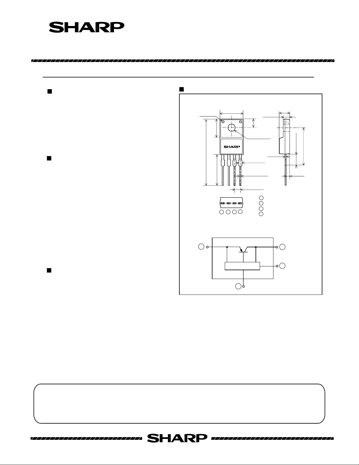
Outline Dimensions
10.2
Front, rear
4-(ø1.4)
0.2
±
MAX
7.4
PQ6RD083
MAX
29.1
13.5 MIN
1
23
Mold package
1
Input
3-(2.54)
4
4.5±0.2
±0.2
2.8
±0.2
3.6
ø3.2±0.1
(0.5)
+0.3
4-1.4
-0
+0.2
4- 0.6
-0.1
( ): Typical values
1 DC input(Vin)
2 DC output(Vo)
3 GND
4 ON/OFF control terminal(Vc)
2
Output
(Unit: mm)
4.8 MAX
15.6±0.5
(1.5)
Applications
(1) CRT displays
(2) Power supplies for various electronic equipment
Specific IC
3
GND
4
ON/OFF control
teminal
such as AV, OA
(Notice)
• In the absence of device specification sheets, SHARP takes no responsibility for any defects that may occur in equipment using any SHARP devices
shown in catalogs, data books, etc. Contact SHARP in order to obtain the latest device specification sheets before using any SHARP device.
• Specifications are subject to change without notice for improvement.
(Internet)
• Data for Sharp's optoelectronic/power devices is provided for internet. ( Address http://www.sharp.co.jp/ecg/)
Tec.PW961101
PQ6RD083
Low Power-Loss Voltage Regulator
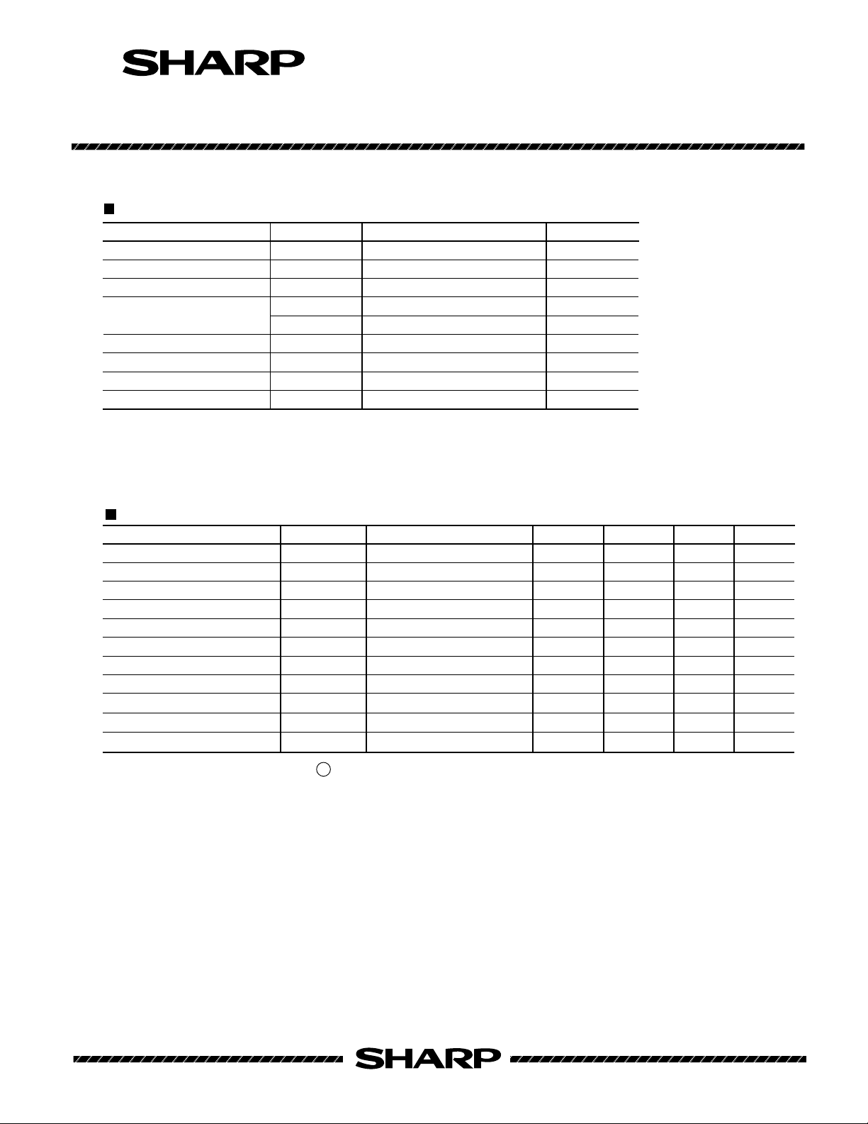
Absolute Maximum Ratings
Parameter Symbol Rating
in
*1 Input voltage
ON/OFF control terminal voltage
*1
Output current I
*2 Power dissipation
*3 Junction temperature T
Operating temperature
Storage temperature T
Soldering temperature T
V
VC 20
o 0.8 A
P
D1 1.25 W
D2 10 W
P
j
opr
T
stg
sol
*1 All are open except GND and applicable terminals.
*2 Pd1: No heat sink, Pd2: With infinite heat sink
*3 Overheat protection may operate at 125<=Tj<=150˚C.
Electrical Characteristics
Parameter Symbol Conditions
Output voltage V
Load regulation
Line regulation R
Temperature coefficient of output voltage
o − 6.111
R
egL Io=5mA to 0.8A
egI Vin=7 to 13V,Io=5mA
TcVo
Ripple rejection RR
*4 ON-state voltage for control
ON-state current for control
OFF-state voltage for control
OFF-state current for control
Vc(on)
Ic(on)
Vc(off)
Ic(off)
Dropout voltage Vi-o
q
Quiescent current
I
20 V
150 ˚C
−20 to +80 ˚C
−40 to +150 ˚C
260(For 10s) ˚C
(Unless otherwise specified, Vin=8V, Io=0.5A, Ta=25˚C)
Tj=0 to 125˚C, Io=5mA
− 45
−
Vc=2.7V
−
Vc=0.4V
*5, Io=0.5A
Io=0A
(Ta=25˚C)
Unit
V
MIN.
−
−
−
2.0
−−
−−
−−
−−
TYP. MAX. Unit
6.3
6.489
0.1 2.0 %
0.1 2.5
±0.02
55
−
−
−
−
20
0.8
-0.4
0.5
−−10 mA
V
%
%/˚C
dB
V
µA
V
mA
V
*4 In case of opening control terminal 4 , output voltage turns on.
*5 Input voltage shall be the value when output voltage is 95% in comparison with the initial value.
As of November 1996
Tec.PW961101
 Loading...