Sharp PC729 Datasheet

PC729
PC729
Bi-directional Output Type
Photocoupler
■ Features
1. Bi-directional output type
2. High collector-emitter voltage (V
3. High collector output current (I
: 300V
BR
: 150mA
O
4. High isolation voltage between input and
output (V
: 5 000V
iso
)
rms
■ Applications
1. Telephone sets
2. Measuring instruments
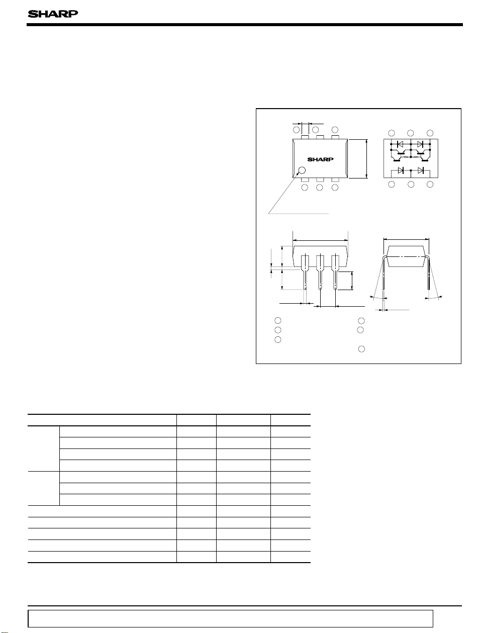
■ Outline Dimensions
± 0.3
)
1.2
456
)
PC729
123
Anode mark
(
Sunken mark
± 0.5
3.5
0.5TYP.
± 0.3
3.4
± 0.1
0.5
1 Anode
2 Anode, Cathode
3 Cathode
9.22
)
± 0.5
2.54
Internal connection
diagram
± 0.5
6.5
*Terminal No. 5
± 0.3
3.1
± 0.25
θ
4 V
O
* 5 May not be externally
connected
6 V
O
(
Unit : mm
*
654
123
represents NC terminal
when AC operated.
± 0.3
7.62
θ=0 to 13˚
± 0.1
0.26
)
θ
■ Absolute Maximum Ratings
(
Ta= 25˚C
)
Parameter Symbol Rating Unit
Forward current I
*1
Input
Peak forward current I
Reverse voltage V
Power dissipation P
Breakdown voltage V
Output
Output current I
Power dissipation P
Total power dissipation P
*2
Isolation voltage V
Operating temperature T
Storage temperature T
*3
Soldering temperature T
*1 Pulse width <=100µs, Duty ratio : 0.001
*2 40 to 60% RH, AC for 1 minute
*3 For 10 seconds
“ In the absence of confirmation by device specification sheets, SHARP takes no responsibility for any defects that occur in equipment using any of SHARP's devices, shown in catalogs,
data books, etc. Contact SHARP in order to obtain the latest version of the device specification sheets before using any SHARP's device.”
F
FM
R
13
BR
O
46
tot
iso
opr
stg
sol
30 mA
1A
6V
80 mW
300 V
150 mA
370 mW
400 mW
5 000
V
rms
- 25 to + 85 ˚C
- 55 to+ 125 ˚C
260 ˚C

PC729
■ Electro-optical Characteristics
Parameter Symbol Conditions MIN. TYP. MAX. Unit
*4
Forward voltage
Input
Output
Transfer
charac-
teristics
*4 Between terminals 1 and 2, and between terminals 2 and 3
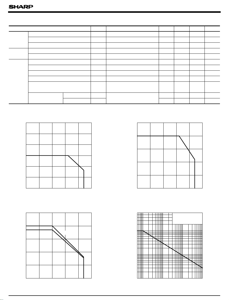
Fig. 1 Forward Current vs.
Ambient Temperature
)
mA
(
Forward current I
*4
Reverse current VR=4V - - 10 µA
*4
Terminal capacitance V = 0, f= 1kHz - 30 250 pF
Collector dark current V
Breakdown voltage I
Output current
ON-state voltage
Isolation resistance 5 x 10
Floating capacitance V= 0, f= 1MHz - 1.0 - pF
Cut-off frequency
Response time
60
50
40
F
30
20
10
Rise time
V
IF= 10mA - 1.2 1.4 V
F
I
R
C
t
I
d
V
BR
I
O
V
on
R
ISO
C
f
f
c
t
r
t
f
= 200V, IF=0 - -
46
= 0.1mA, IF= 0 300 - - V
O
I
= 1mA, V46=3V
F13
= 20mA, IO= 100mA
I
F13
DC500V, 40 to 60%RH
= 3V, IO= 20mA
V
46
R
= 100 Ω, - 3dB
L
V
= 3V, IO= 20mA
46
R
= 100 Ω
L
10 40 150 mA
- 1.8 2.4 V
101011
1 7 - kHz
- 50 300 µ s
- 20 100 µ sFall time
Fig. 2 Input Power Dissipation vs.
Ambient Temperature
100
)
80
mW
(
13
60
40
20
Input power dissipation P
(
Ta= 25˚C
-6
10
- Ω
)
A
0
Ambient temperature Ta (˚C
Fig. 3 Power Dissipation vs.
Ambient Temperature
)
400
mW
(
370
tot
, P
300
46
200
100
Power dissipation P
0
-25
0 25507510085
Ambient temperature Ta (˚C
P
P
46
85
1007550250-25
)
0
- 25 0 25 75 100
Ambient temperature Ta (˚C
50
85
)
Fig. 4 Peak Forward Current vs. Duty Ratio
5
)
3
mA
10
(
tot
)
FM
5
2
10
5
Peak forward current I
1
10
-3
5252525
10
-2
10
Duty ratio
Pulse width<=100µs
Ta= 25˚C
-1
10
1
 Loading...