

Sharp PC727 Datasheet
PC727
PC727
Low Input Current Drive Type
Photocoupler
Features
1. Low input current drive type (IF : 50 µA)
2. Current transfer ratio (CTR : MIN. 60%)
Assured within operating temperature range (Ta=-25 to +60˚C)
■
Applications
1. ISDNs
2. Telephone sets
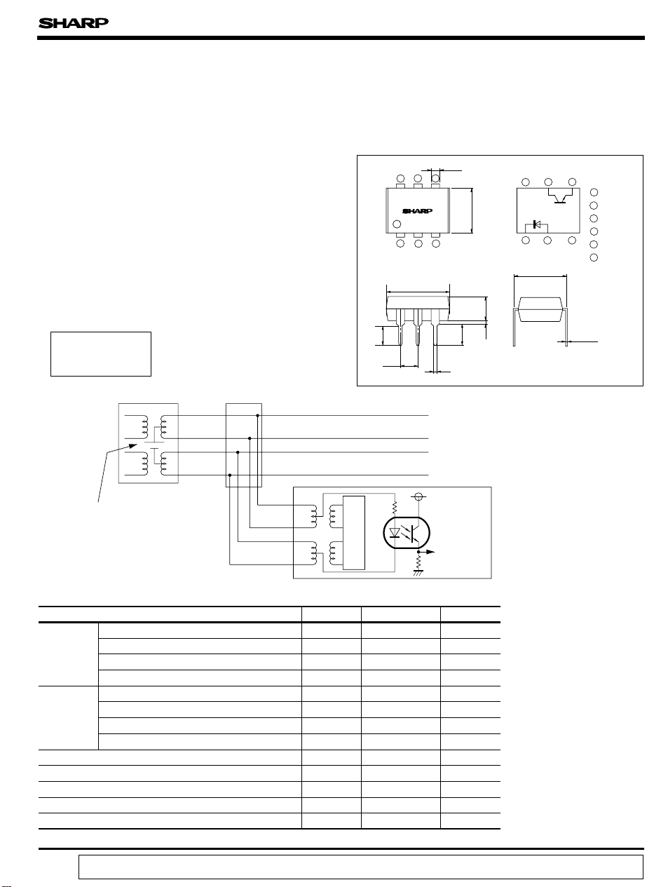
Example of ISDN
terminal configuration
DSU Modular jack
Send
Receive
TE terminal
Feed (from station) :
40V (+5/-20%)
(32 to 42V)
Receive
Send
■■
Outline Dimensions
4
56
PC727
123
9.22
3.4
2.54
Rotary driver
/receiver IC
0.5
* DSU :
* TE terminal :
5V
PC727
connection
detection to
C-MOS IC
(Unit : mm)
1.2
Internal connection diagram
6.5
3.7
Digital Service Unit (line terminal equipment)
Terminal Equipment (standard terminal)
3.50.5
654
321
7.62
0.26
1 Cathode
2 Anode
3 NC
4 Emitter
5 Collector
6 NC
■
Absolute Maximum Ratings
*1
Parameter Symbol Unit
Forward current I
*2
Input
Peak forward current
Reverse voltage
*1
Power dissipation mW
Collector-emitter voltage V
Output
Emitter-collector voltage V
Collector current I
*3
Collector power dissipation P
*3
Total power dissipation 170 mW
Operating temperature - 30to + 100 ˚C
Storage temperature ˚C
*4
Isolation voltage
*5
Soldering temperature
“ In the absence of confirmation by device specification sheets, SHARP takes no responsibility for any defects that occur in equipment using any of SHARP's devices, shown in catalogs,
data books, etc. Contact SHARP in order to obtain the latest version of the device specification sheets before using any SHARP's device.”
F
I
FM
V
R
I
CEO
CEO
ECO
C
C
P
tot
T
opr
T
stg
V
iso
T
sol
Rating
5
300
6V
40
35 V
6V
50 mA
150 mW
- 55to + 125
2 500
260 ˚C
(Ta=25˚C)
mA
mA
Vrms
*1 Ta=-30 to +100˚C
*2 Pulse width<=100 µs,
Duty ratio=0.01 (Refer to Fig. 3)
*3 Decrease in the ambient temperature
range of the Absolute Max. Rating :
Shown in Figs.1 and 2.
*4 40 to 60% RH, AC for 1 minute
*5 For 10 seconds
PC727
Electro-optical Characteristics
■
Parameter Symbol Conditions Unit
Forward voltage V
Input
Peak forward voltage I
Reverse current I
Terminal capacitance V= 0, f= 1kHz - 80 - pF
*6
Output
Transfer
characteristics
Dark current I
Collector-emitter breakdown voltage
Emitter-collector breakdown voltage
*6
Collector current IF=50µA, VCE=5V 30 - - µA
Collector-emitter saturation voltage V
Insulation resistance R
Cut-off frequency V= 0, f= 1MHz - 0.6 - pF
Response time (rise)
Response time (fall) - 25 -
*6 Ta= - 25to + 60˚C
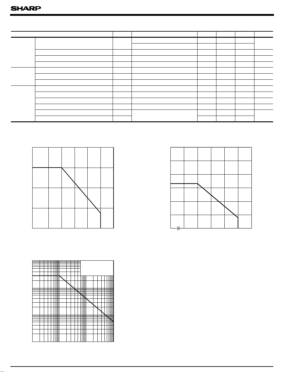
Fig. 1 Collector Power Dissipation vs.
Ambient Temperature
200
150
100
50
Collector power dissipation Pc (mW)
0
0 125
25 50 75 100-30
BV
BV
IF=50µA - 1.2 -
F
I
= 5mA - 1.4 1.6
F
V
C
CEO
I
CE(sat
f
FM
ISO
t
t
R
t
CEO
ECO
c
c
r
f
= 300mA - - 2 V
FM
VR=4V - - 10 µA
VCE= 10V, IF=0 - - 3 µA
Ic= 0.1mA, IF= 0 35 - - V
IE= 0.01mA, IF=0
)
I
= 100µ A, Ic=50µA
F
6--V
--1V
DC500V, 40to 60%RH 5 x 10101x1011- Ω
VCE= 2V, Ic= 2mA
= 100Ω
R
L
-20-
Fig. 2 Total Power Dissipation vs.
Ambient Temperature
250
200
170
150
100
50
Total power dissipation Ptot (mW)
0
0 25 50 75 100 125
-30
Ambient temperature Ta (˚C)Ambient temperature Ta (˚C)
MIN. TYP. MAX.
(Ta=25˚C)
V
µs
Fig. 3 Peak Forward Current vs. Duty Ratio
1 000
500
200
FM
100
50
20
10
5
Peak forward current I (mA)
2
1
-3
10
Please refer to the chapter "Precautions for Use."
●
-2
10
Duty ratio
Pulse width<=100 µs
Ta= 25˚C
-1
10
0
10
 Loading...