

High Sensitivity, High
PC725V
Collector-emitter Voltage
Type Photocoupler
❈ Lead forming type (W type) and taping reel type (P type) are also available. (PC725W/PC725VP)
..
❈❈ TUV (VDE0884) approved type as an option is also available.
■ Features
1. High collector-emitter voltage
(V
CEO
: 300V
)
2. High current transfer ratio
(CTR : MIN. 1 000% at I
= 1mA, VCE=2V
F
3. High isolation voltage between input and
output (V
: 5 000V
ISO
)
rms
4. Low collector dark current
(I
: MAX. 10-6A at VCE= 200V
CEO
)
5. Recognized by UL, file No. E64380
■ Applications
1. Telephone sets, telephone exchangers
2. Power apparatus switchboards
3. Numerical control machines
4. DC-DC SSRs, DC motor controllers
)
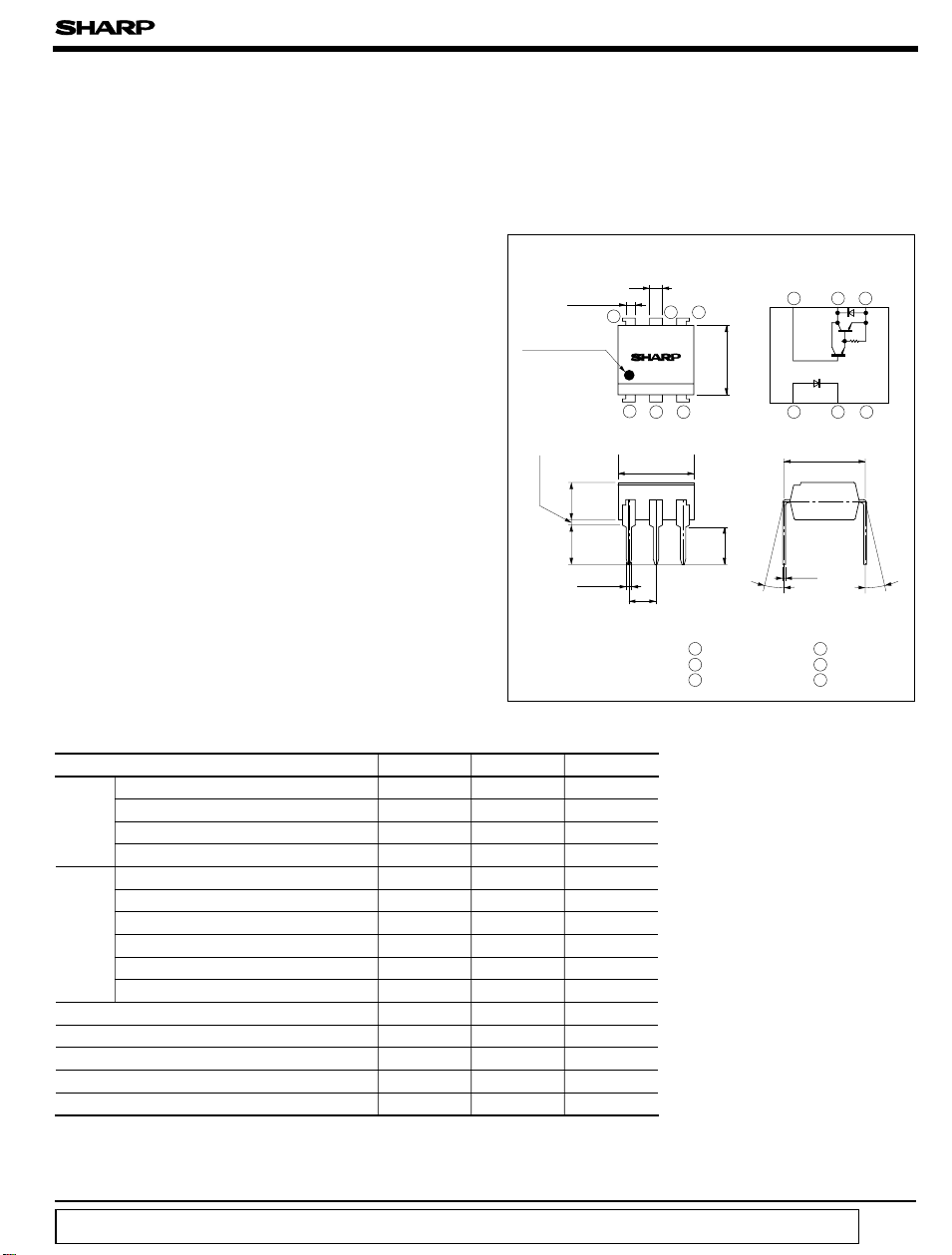
■ Outline Dimensions
± 0.3
1.2
± 0.2
0.9
Anode mark
± 0.5
0.5TYP
3.5
± 0.5
3.7
0.5
± 0.1
2.54
6
PC725V
123
7.12
± 0.25
54
± 0.5
± 0.5
6.5
± 0.5
Internal connection
diagram
654
123
7.62
θ = 0 to 13˚
3.35
0.26
PC725V
(
Unit : mm
± 0.3
± 0.1
)
θθ
1 Anode
2 Cathode
3 NC
V
)
mA
rms
˚C
˚C
■ Absolute Maximum Ratings
Parameter
Forward voltage
*1
Input
Peak forward voltage
Reverse current
Power dissipation
Collector-emitter voltage
Collector-base voltage
Output
Emitter-base voltage
Collector current
Collector current (reverse
)
Collector power dissipation
Total power dissipation
*2
Isolation voltage
Operating temperature
Storage temperature
*3
Soldering temperature
*1 Pulse width<=100µs, Duty ratio : 0.001
*2 40 to 60%RH, AC for 1 minute
*3 For 10 seconds
“ In the absence of confirmation by device specification sheets, SHARP takes no responsibility for any defects that occur in equipment using any of SHARP's devices, shown in catalogs,
data books, etc. Contact SHARP in order to obtain the latest version of the device specification sheets before using any SHARP's device.”
Symbol Rating Unit
I
F
I
FM
V
R
P70mW
V
CEO
V
CBO
V
EBO
I
C
-I
C
P
C
P
tot
V
iso
T
opr
T
stg
T
sol
5 000
- 25 to + 100
- 40 to + 125
(
= 25˚C
T
a
50 mA
1A
6V
300 V
300 V
6V
150 mA
10
300 mW
350 mW
260 ˚C
4 Emitter
5 Collector
6 Base
PC725V
■ Electro-optical Characteristics
Parameter Symbol Conditions MIN. TYP. MAX. Unit
Forward voltage
Input
Peak forward voltage
Reverse current
Terminal capacitance
Output Collector dark current I
Current transfer ratio CTR I
Collector-emitter saturation voltage
Transfer
charac-
teristics
Isolation resistance R
Floating capacitance C
Cut-off frequency f
Response time
Rise time
Fall time
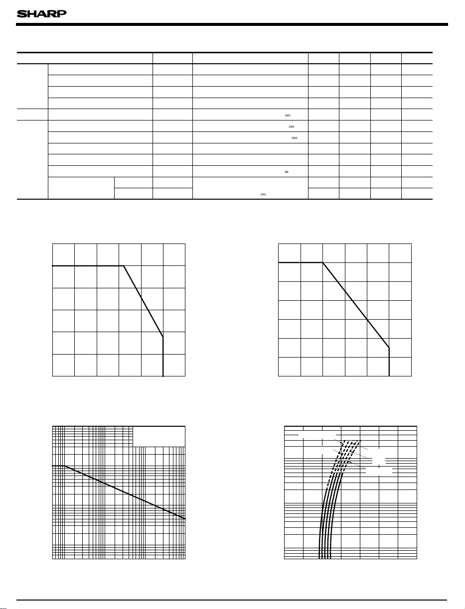
Fig. 1 Forward Current vs.
Ambient Temperature
60
50
)
mA
40
(
F
20
Forward current I
10
0
-25300 25 50 75 100 125
Ambient temperature Ta (˚C
Fig. 3 Peak Forward Current vs. Duty Ratio
10 000
5 000
)
2 000
mA
1 000
(
FM
500
200
100
50
20
Peak forward current I
10
5
-3
2
5
10
5
10
Duty ratio
-2
2
Pulse width <=100 µs
Ta= 25˚C
5
V
F
V
FM
I
R
C
t
CEO
V
CE(sat
ISO
f
c
t
r
t
f
)
-1
2
10
5
(
Ta= 25˚C
)
IF= 10mA - 1.2 1.4 V
IFM= 0.5A - - 3 V
VR=4V - - 10 µA
V= 0, f = 1kHz - 30 250 pF
VCE= 200V, IF= 0, RBE=--10-6A
= 1mA, VCE= 2V, RBE=%
F
)
IF= 20mA, IC= 100mA, RBE=
DC500V, 40 to 60%RH
1 000 4 000 15 000
- - 1.2 V
5x101010
11
- Ω
V= 0, f = 1MHz - 0.6 1.0 pF
VCE= 2V, IC= 20mA, RL= 100Ω, RBE= , - 3dB
VCE= 2V, IC= 20mA
= 100Ω, RBE=
R
L
1 7 - kHz
- 100 300 µs
- 20 100 µs
Fig. 2 Collector Power Dissipation vs.
Ambient Temperature
350
)
300
mW
(
C
250
200
150
100
Collector power dissipation P
50
0
- 25 0 25 50 75 100 125
Ambient temperature Ta (˚C
)
Fig. 4 Forward Current vs.
Forward Voltage
500
200
100
)
50
mA
(
F
20
10
Forward current I
1
T
= 75˚C
a
50˚C
5
2
1
0
0.5 1.0 1.5 2.0 2.5 3.0 3.5
Forward voltage VF (V
25˚C
0˚C
- 25˚C
)
PC725V
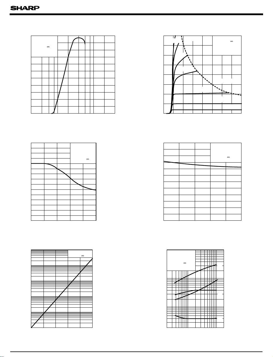
Fig. 5 Current Transfer Ratio vs.
Forward Current
=2V
V
5 000
)
%
(
4 000
CE
RBE=
T
a
= 25˚C
3 000
2 000
Current transfer ratio CTR
1 000
0
0.2 0.5 1 2 5 10 20
0.1
)
Forward current I
F
(mA
Fig. 7 Relative Current Transfer Ratio vs.
Ambient Temperature
150
)
%
(
100
50
I
F
V
R
= 1mA
CE
BE
=2V
=
Fig. 6 Collector Current vs.
Collector-emitter Voltage
160
= 5mA
(mA)
C
140
120
100
I
F
3mA
2mA
1.5mA
=
R
BE
=
25˚C
Ta
80
P
( MAX.)
60
40
Collector current I
20
0
12345678
0
Collector-emitter voltage VCE (V
C
1mA
0.7mA
0.5mA
)
Fig. 8 Collector-emitter Saturation Voltage
vs. Ambient Temperature
1.2
)
V
(
)
sat
1.0
(
CE
0.8
0.6
0.4
= 20mA
I
F
= 100mA
I
C
R
BE
=
Relative current transfer ratio
0
0 25 50 75 100
-25
Ambient temperature Ta (˚C
Fig. 9 Collector Dark Current vs.
Ambient Temperature
-4
10
-5
10
)
A
(
CEO
-6
10
-7
10
-8
10
Collector dark current I
-9
10
-25
0
Ambient temperature Ta (˚C
25
VCE= 200V
=
R
BF
50 75 100
)
0.2
Collector-emitter saturation voltage V
0
)
- 25 0 25 50 75 100
Ambient temperature T (˚C
)
a
Fig.10 Response Time vs. Load Resistance
1000
500
200
)
100
µ s
(
50
20
Response time
10
=2V
V
CE
= 20mA
I
C
=
R
T
BE
= 25˚C
a
t
t
5
2
0.02 0.05 0.1 0.2 0.5 1 2
)
Load resistance R
L
(kΩ
r
d
t
f
t
s

PC725V
Test Circuit for Response Time
V
Input
CC
R
D
R
L
Output
Input
Output
t
d
Test Circuit for Frepuency Response
V
CC
R
D
R
L
Output
Fig.10 Frequency Response
VCE=2V
I
= 20mA
100Ω
201052
R
T
C
BE
a
=
= 25˚C
10Ω
50 100
0
)
dB
-5
(
10%
t
t
r
90%
s
t
r
v
-10
-15
Voltage gain A
RL=1kΩ
-20
0.05 0.1 0.2 0.5
1
Frequency f (kHz
)
Please refer to the chapter “Precautions for Use ”
●
.
 Loading...