

Sharp PC724V Datasheet
High Input Current Type
PC724V
❈ Lead forming type (W type) and taping reel type (P type) are also available. (PC724W/PC724VP)
Photocoupler
PC724V
■ Features
1. High input current (IF: MAX. 150mA
2. High isolation voltage between input and
output
(V
: 5 000V
iso rms
)
3. Standard dual-in-line package
4. Recoginzed by UL, file no. E64380
■ Applications
1. Telephone sets
2. I/O interfaces for microcomputer
3. System appliances, measuring instru ments
4. Signal transmission between circuits of
different potentials and impedances
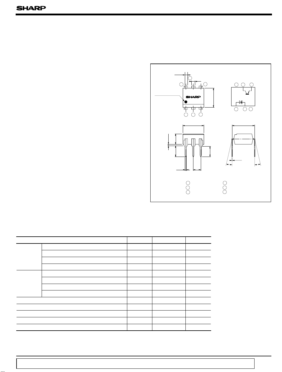
■ Outline Dimensions
)
Anode mark
TYP.
0.5
0.9
± 0.5
3.5
± 0.5
3.7
0.5
± 0.2
6
PC724V
123
7.12
± 0.1
1 Anode
2 Cathode
3 NC
5
2.54
± 0.5
1.2
± 0.25
± 0.3
4
± 0.5
± 0.5
6.5
3.35
(
Unit : mm
Internal connection
diagram
65 4
123
± 0.3
7.62
± 0.1
0.26
θ = 0 to 13 ˚
4 Emitter
5 Collector
6 NC
)
θθ
■ Absolute Maximum Ratings
(
Ta= 25˚C
)
Parameter Symbol Rating Unit
Input
Forward current I
*1
Peak forward current I
Reverse voltage V
F
FM
R
150 mA
1A
6V
Power dissipation P 230 mW
Collector-emitter voltage V
Output
Emitter-collector voltage V
Collector current I
Collector power dissipation P
Total power dissipation P
*2
Isolation voltage V
Operating temperature T
Storage temperature T
*3
Soldering temperature T
*1 Pulse width<=100µs, Duty ratio : 0.001
*2 40 to 60%RH, AC for 1 minute
*3 For 10 seconds
“ In the absence of confirmation by device specification sheets, SHARP takes no responsibility for any defects that occur in equipment using any of SHARP's devices, shown in catalogs,
data books, etc. Contact SHARP in order to obtain the latest version of the device specification sheets before using any SHARP's device.”
CEO
ECO
C
C
tot
iso
opr
stg
sol
35 V
6V
80 mA
160 mW
320 mW
5 000
V
rms
- 25 to + 100 ˚C
- 55 to + 125 ˚C
260 ˚C
PC724V
■ Electro-optical Characteristics
Parameter Symbol Conditions MIN. TYP. MAX. Unit
Forward voltage V
Input
Peak forward voltage V
Reverse current I
Terminal capacitance C
Output Collector dark current I
Current tranfer ratio CTR I
Collector-emitter saturation voltage
Transfer
charac-
teristics
Isolation resistance R
Floating capacitance C
Cut-off frequency f
Response time
Rise time
Fall time
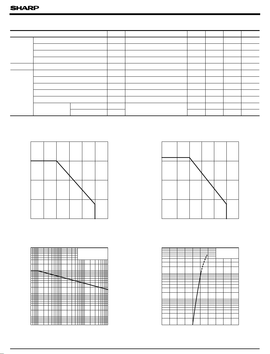
Fig. 1 Forward Current vs.
Ambient Temperature
200
)
150
mA
(
F
100
FIF
FMIFM
R
t
CEOVCE
V
CE(sat
ISO
f
cVCE
t
r
t
f
(
Ta= 25˚C
= 100mA - 1.4 1.7 V
= 0.5A - - 3.0 V
VR=4V - - 10 µA
V= 0, f= 1kHz - 30 250 pF
11
-7
- Ω
A
= 20V, IF=0 - - 10
= 100mA, VCE= 2V 20 - 80 %
F
)
IF= 100mA, IC= 1mA - 0.1 0.2 V
DC500V, 40 to 60%RH
5x10101x10
V= 0, f= 1MHz - 0.6 1.0 pF
= 5V, IC= 2mA, RL=100Ω, - 3dB
- 100 - kHz
VCE= 5V, IC= 2mA - 4 18 µ s
RL= 100Ω -318µs
Fig. 2 Collector Power Dissipation vs.
Ambient Temperature
200
)
160
mW
(
150
C
100
)
Forward current I
0
-25500 25 50 75 100 125
Ambient temperature T
(˚C)
a
Fig. 3 Peak Forward Current vs. Duty Ratio
10 000
5 000
)
2 000
mA
1 000
(
FM
500
200
100
50
20
Peak forward current I
10
-3
10
10
Duty ratio
-2
Pulse width <=100 µs
Ta= 25˚C
-1
10
1
50
Collector power dissipation P
0
-25
0 125
25 50 75 100
Ambient temperature T
Fig. 4 Forward Current vs.
Forward Voltage
1 000
500
)
200
mA
(
100
F
50
20
10
Forward current I
5
2
1
0
0.5 1.0 1.5 2.0 2.5
Forward voltage V
(˚C)
a
= 25˚C
T
a
(V)
F
 Loading...