Sharp PC3Q67 Datasheet

.
PREPARED BY:
DATE
I-), Ti&Grr~A qp-; I 9 1993
APPROVED BY: DATE
c-
’ ?.
,., f ,I.. it!.. ,I
.r
/: s
! ,;
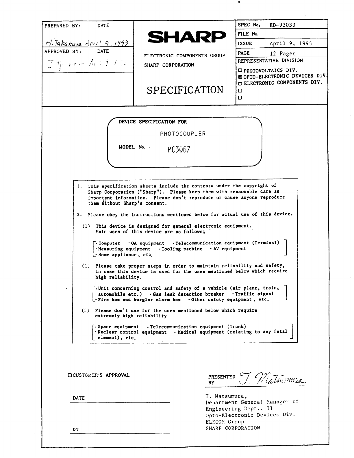
SPEC No.
FILE No.
SHARI=
_ - -- -- ~~
ELECTRONIC COMPONENTS CROUP
SHARP CORPORATION
I
ISSUE April 9, 1993
PAGE
REPRESENTATIVE DIVISION
q
q
n
1 SPECIFICATION 10
ED-93033
12 Pages
PHOTOVOLTAICS DIV.
OPTO-ELECTRONIC DEVICES DJV
ELECTRONIC COMPONENTS DIV.
’ DEVICE SPECIFICATION FOR
PHOTOCOUPLER
hiODEL No.
1. This
2. Dlease obey the instructions mentioned below for actual use of this device.
(1) This device is designed for general electronic equipment.
(Zj Please take proper steps in order to maintain reliability and safety,
specification sheets include the contents under the copyright of
sharp
Corporation (“Sharp”).
important
:hem \;i’thout Sharp’s consent.
Main uses of this device are as follows; .
- Computer C * OA equipment -Telecommunication equipment (Terminal)
- Measuring equipment -Tooling machine
- Home appliance, etc.
in case this device is used for the uses mentioned below which require
high reliability.
information. Please don’t reproduce or cause anyone reproduce
Please keep them with reasonable care as
* AV equipment
w
1
-Unit concerning control and safety of a vehicle (air plane, train,
automobile etc.) * Gas leak detection breaker
i
-Fire box and burglar alarm box
(2) Please don’t use for the uses mentioned below which require
extremely high reliability
Telecommunication equipment (Trunk)
element), etc.
0 CLJSTG:6RR’S APPROVAL
DATE
BY
*Other safety equipment, etc..
Medical equipment (relating to any fatal
T. Matsumura,
Department General Manager of
Engineering Dept., TI
Opto-Electronic Devices Div.
ELECOM Group
SHARP CORPORATION
- Traffic signal
I
1

MODEL No. PACE
i.
Application
This specification applies to the outline and characteristics of
photocoupler Model No. PC3Q67.
2. Outline
Refer to the attached drawing No. CY5890K02.
Ratings and characteristics
3.
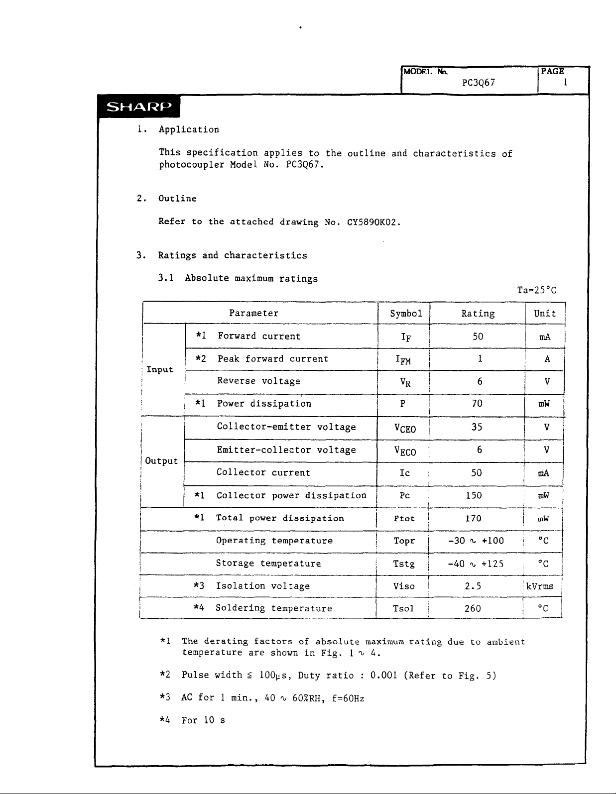
3.1 Absolute maximum ratings
PC3Q67 1
Ta=25"C
iInput /
/
I
ioutput
!
!
1
Parameter
--------_
*1 Forward current
Symbol Rating Unit ,
IF j
50 mA
*2 Peak forward current / Im 1 1 / A
!
Reverse voltage
"R f
6
,
; *1 Power dissipation
Collector-emitter voltage
Emitter-collector voltage
P 1 70 mW
"CEO
VECO )
35
6
Collector current Ic i 50
*l Collector power dissipation
150 mW
/2..-- j
*l Total power dissipation
I
Ptot !
!
170
Operating temperature ' Topr 1 i -30 % +lOO ! OC
___-
Storage temperature
i Tstg 1 -40 'L +125
I
-__-_-_--______
*3 Isolation voltage
-_~.---
*4 Soldering temperature
--- ___. --__
I
V
" i
( "1
1
I * 1
I
i LUW '
j
*1 The derating factors of absolute maximum rating due to ambient
temperature are shown in Fig. 1 'L 4.
*2 Pulse width < lOOus, Duty ratio : 0.001 (Refer to Fig. 5)
*3 AC for lmin.,
40 ,-I, 60%RH, f=60Hz
*4 For 10 s

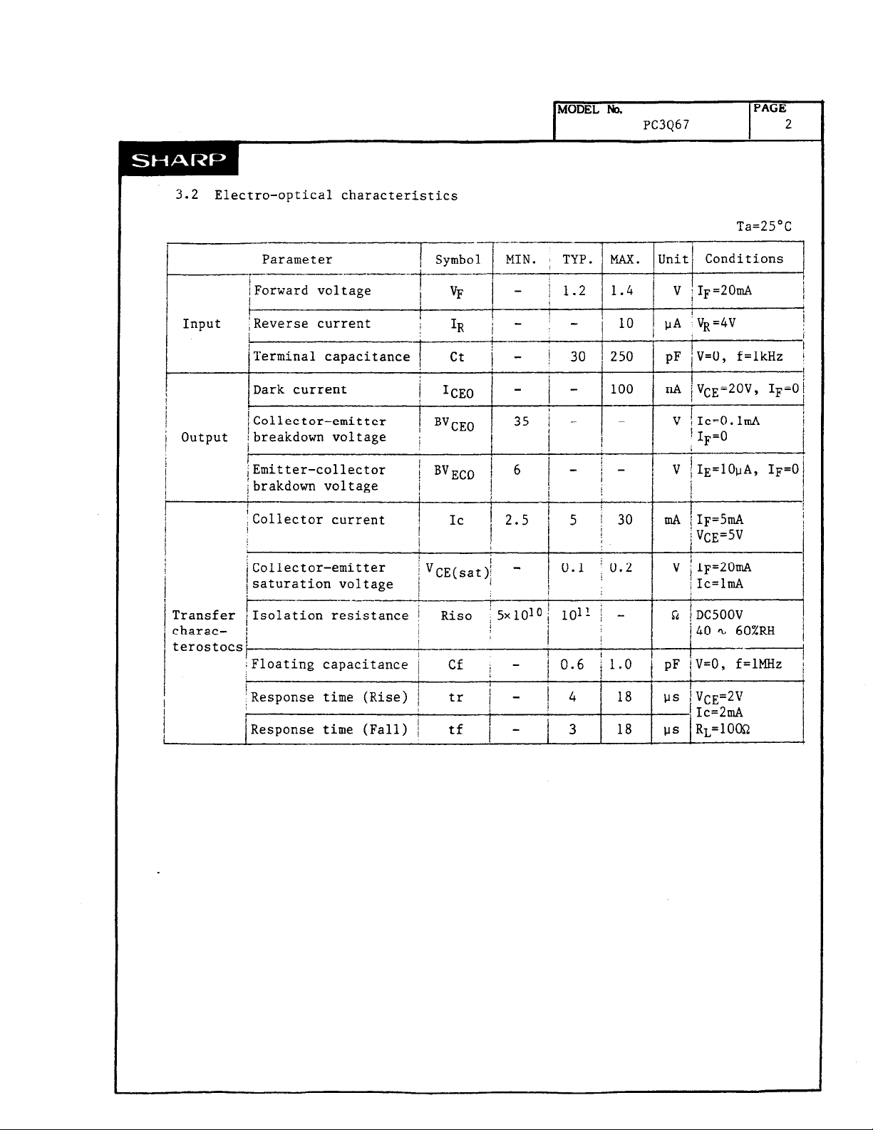
3.2 Electra-optical characteristics
MODEL hb.
PC3Q67
PACE
l
2
Input
output
Transfer
characterostocs
Parameter Symbol
----.---+---
-1
Forward voltage
I
Reverse current
Terminal capacitance
Dark current
/ ICE0 / -
Collector-emitter
breakdown voltage 1
I
i
Emitter-collector
I
brakdown voltage
Collector current
Collector-emitter
saturation voltage
------Isolation resistance
----T----- ,
Ta=25"C
MIN. I TYP. MAX.
VF -
i 1.2 1.4
1 v ?F=20mA
! I
Unit Conditions
' 10 1 pA ‘VR=4V
f
/ -
I 250
100
'V=O, f=lkHz i
pF I
ti /vCE=20v, IF'0 1
i
I
I
I
I
!
Response time (Rise) tr
r
L
Response time (Fall) I tf / -
/
j- 14 18 1 US jVCE=2V
,
3
18 ps RL=lOOQ
'Ic=2mA
j
I

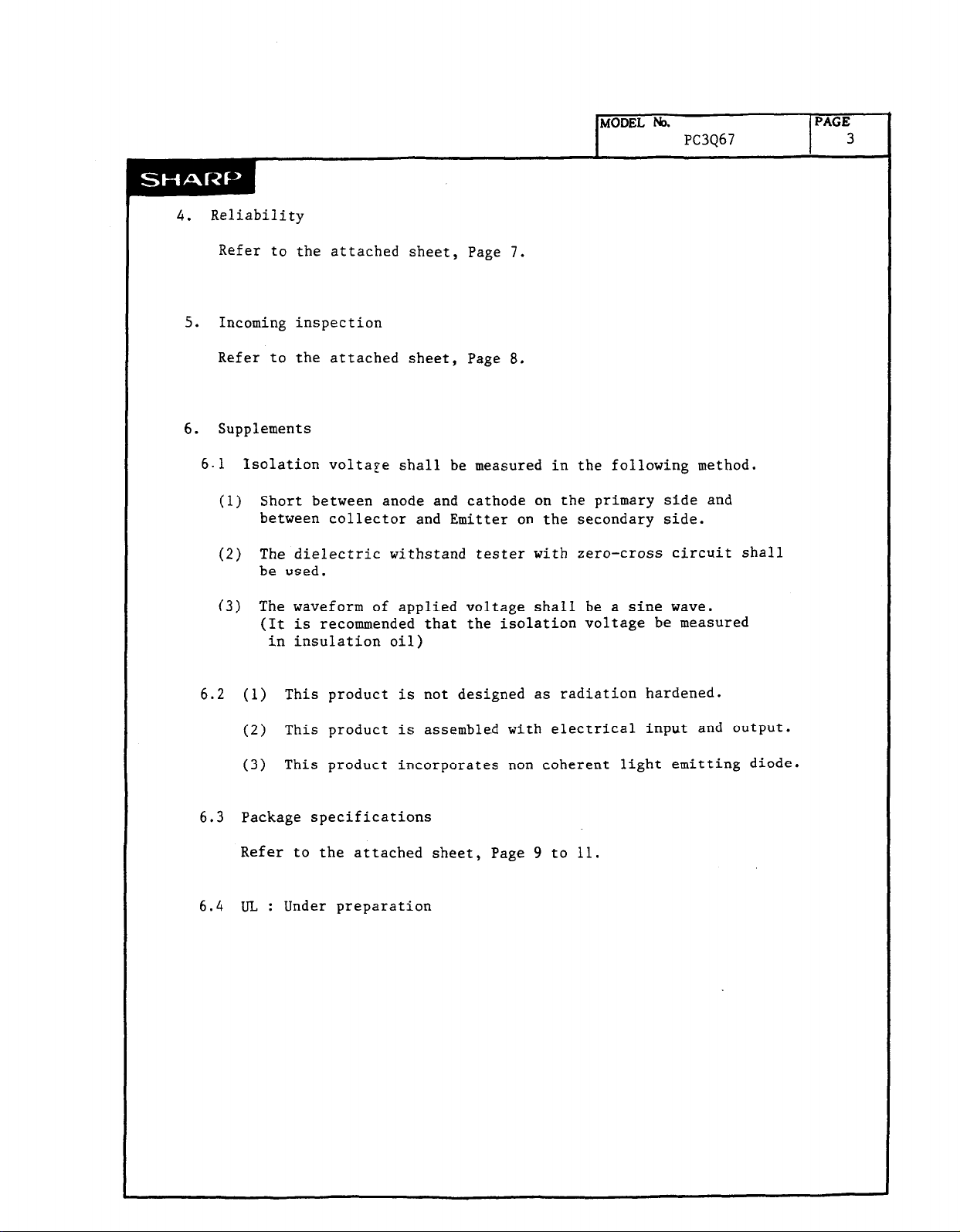
4. Reliability
Refer to the attached sheet, Page 7.
5. Incoming inspection
Refer to the attached sheet, Page 8.
6. Supplements
6.1
Isolation voltape shall be measured in the following method.
1) Short between anode and cathode on the primary side and
(
between collector and Emitter on the secondary side.
(2) The dielectric withstand tester with zero-cross circuit shall
be used.
(3) The waveform of applied voltage shall be a sine wave.
(It is recommended that the isolation voltage be measured
in insulation oil)
6.2 (1) This product is not designed as radiation hardened.
(2) This product is assembled
with
electrical input and output.
(3) This product incorporates non coherent light emitting diode.
6.3 Package specifications
Refer to the attached sheet, Page 9 to 11.
6.4 uL
: Under preparation
 Loading...