

PC3H4/PC3Q64Q
PC3H4/PC3Q64Q
■ Features
1. AC input type
2. Half pitch type (lead pitch : 1.27mm)
3. Isolation voltage between input and output
(Viso: 2 500Vrms)
4. Applicable to infrared ray reflow
(230˚C, for MAX. 30s)
5. High reliability
6. Taping package
PC3H4 (1ch), PC3Q64Q (4ch)
7. Recognized by UL, file No. E64380
Approved by VDE, No.5922UG
■ Applications
1. Programmable controllers
■ Package Specifications
Model No.
PC3H4
PC3Q64Q
Taping reel diameter 330mm (3 000pcs.)
Taping reel diameter 330mm (1 000pcs.)
■ Absolute Maximum Ratings
Parameter Rating
Forward current
*1
Peak forward current
InputOutput
Power dissipation
Collector-emitter
voltage
Emitter-collector voltage
Collector current
Collector power dissipation
Total power dissipation
*2
Isolation voltage
Operating temperature
Storage temperature
*3
Soldering temperature
*1 Pulse width<=100µs, Duty ratio : 0.001
*2 AC for 1min, 40 to 60%RH, f=60Hz
*3 For 10s
Taping specifications
PC3H4
PC3Q64Q
Symbol
I
F
IFM
P
V
CEO
VCEO
VECO
IC
PC
Ptot
Viso
Topr
Tstg
Tsol
±50
±1
70
70
35 V
6
50
150
170
2.5
−30 to +100
−40 to +125
260
Soldering area
(Ta=25˚C)
Unit
mA
A
mW
V
V
mA
mW
mW
kV
rms
˚C
˚C
˚C
0.2mm or more
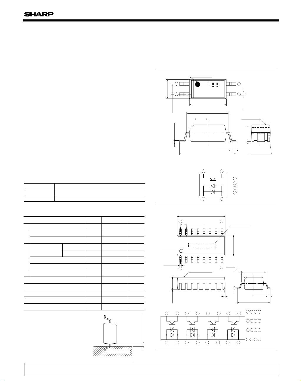
Mini-falt Package AC Input Type
Half Pitch Photocoupler
■ Outline Dimensions
PC3H4
±0.3
2.6
±0.25
1.27
±0.05
❈ ( ) : Reference dimensions
PC3Q64Q
Primary
Side
mark
±
0.1
0.4
0.2
±
2.6
0.1
±
0.1
16 15 14 13 12 11 10
12345678
Anode mark
1
2
0.2
16
1
Internal connection diagram
S
3H4
±0.2
4.4
±0.3
5.3
(1.7)
+0.2
7.0
−0.7
Internal connection diagram
±
0.3
10.3
±
0.25
1.27
Epoxy resin
0.5
+0.4
−0.2
34
21
9
8
6°
Model No.
0.2
±
4.4
C0.4
0.05
±
0.2
1
2
3
4
4
3
±0.1
0.4
Epoxy resin
±0.2
2.0
±0.1
Parting line
0.1
Anode
Cathode
Emitter
Collector
5.3
7.0
1 3 5 7
9
Anode/Cathode
2468
Anode/Cathode
9
11 13 15
Emitter
10 12 14 16
Collector
(Unit : mm)
±
0.3
+0.4
0.5
−0.2
+0.2
−0.7
Notice In the absence of confirmation by device specification sheets, SHARP takes no responsibility for any defects that may occur in equipment using any SHARP
devices shown in catalogs, data books, etc. Contact SHARP in order to obtain the latest device specification sheets before using any SHARP device.
Internet Internet address for Electronic Components Group http://www.sharp.co.jp/ecg/
PC3H4/PC3Q64Q
■ Electro-optical Characteristics
Parameter Conditions
Input
Output
Transfer
charac-
teristics
Forward voltage I
Terminal capacitance
Collector dark current
Collector-emitter I
breakdown voltage
PC3H4
PC3Q64Q
PC3H4
PC3Q64Q
Emitter-collector
breakdown voltage
Collector current
Collector-emitter
saturation voltage
Isolation resistance
Floating capacitance V=0, f=1MHz
Response time
Rise time
Fall time
Symbol
V
F
Ct
ICEO
BVCEO
BVECO
IC
VCE(sat)
RISO
Cf
tr
tf
(Ta=25˚C)
TYP.
1.2
30
−
− −
− −
−
−
0.1
11
0.6
4
3
MAX.
1.4
250
100
−
4.0
0.2
−
1.0
18
18
MIN.
70
35
0.2
5×10
−
−
−
6
−
10
1×10
F=±20mA
V=0, f=1kHz
V
CE=50V, IF=0
V
CE=20V, IF=0 − − 100ICEO nA
C=0.1mA, IF=0
IC=0.1mA, IF=0BVCEO
E=10µA, IF=0
I
F=±1mA
I
V
CE=5V
F=±20mA
I
I
C=1mA
DC500V
40 to 60%RH
−
V
CE=2V
IC=2mA
R
L=100Ω
−
−
Unit
V
pF
nA
V
V
V
mA
V
Ω
pF
µs
µs
Fig.1 Forward Current vs. Ambient
Temperature
60
50
40
(mA)
F
30
20
Forward current I
10
0
−30 0 25 75 100 1255550
Ambient temperature T
(°C)
a
Fig.2 Diode Power Dissipation vs. Ambient
Temperature
100
80
70
60
40
Diode power dissipation P (mW)
20
0
−30 0 55 10050
Ambient temperature T
(°C)
a

PC3H4/PC3Q64Q
Fig.3 Collector Power Dissipation vs.
Ambient Temperature
200
(mW)
150
C
100
50
Collector power dissipation P
0
−30 0 25 50 75 100 125
10000
5000
2000
(mA)
1000
FM
500
200
100
50
Peak forward current I
20
10
5
5 210
Ambient temperature T
−3
5 210
−2
Duty ratio
(°C)
a
Pulse width<=100µs
=25°C
T
a
−1
5 210
5 1
Fig.7 Current Transfer Ratio vs. Forward
Current
500
400
300
200
Current transfer ratio CTR (%)
100
0
0.1 1 10 100
Forward current I
(mA)
F
VCE=5V
=25°C
T
a
Fig.4 Total Power Dissipation vs. Ambient
Temperature
250
200
(mW)
tot
170
150
100
Power dissipation P
50
0
−30 0 25 50 75 100
Ambient temperature T
(°C)
a
Fig.6 Forward Current vs. Forward VoltageFig.5 Peak Forward Current vs. Duty Ratio
500
200
100
50
(mA)
F
20
10
5
Forward current I
1
Ta=75˚C
50˚C
020.5 1.0 1.5 2.0 2.5 3.0 3.5
Forward voltage V
25˚C
0˚C
−25˚C
(V)
F
Fig.8 Collector Current vs. Collector-emitter
Voltage
50
40
(mA)
C
30
20
Collector current I
10
0
0 2 4 6 8 10
PC (MAX.)
IF=30mA
20mA
10mA
Collector-emitter voltage V
5mA
CE
T
1mA
(V)
=25°C
a
PC3H4/PC3Q64Q
Fig.9 Relative Current Transfer Ratio vs.
Ambient Temperature
150
100
50
Relative current transfer ratio (%)
0
−30 0 20 40 60 80 100
Ambient temperature T
a
(°C)
I
F
V
=1mA
=5V
CE
Temperature
−5
10
5
−6
10
5
(A)
−7
CEO
10
5
−8
10
5
−9
10
5
Collector dark current I
−10
10
5
−11
10
−30 0 20 40 60 80 100
Ambient temperature T
a
(°C)
V
=20V
CE
Fig.10 Collector-emitter Saturation
Voltage vs. Ambient Temperature
0.16
0.14
0.12
0.10
(sat) (V)
CE
0.08
0.06
voltage V
Collector-emitter saturation
0.04
0.02
0.00
−30 0 20 40 60 80 100
Ambient temperaturet T
(°C)
a
I
=20mA
F
IC=1mA
Fig.12 Response Time vs. Load ResistanceFig.11 Collector Dark Current vs. Ambient
1000
Response time (µs)
=2V
V
CE
500
=2mA
I
C
=25°C
T
200
a
100
50
20
10
5
2
1
t
r
t
d
t
f
t
s
0.5
0.2
0.1
0.01 0.1 1 10 100
Load resistance RL (kΩ)
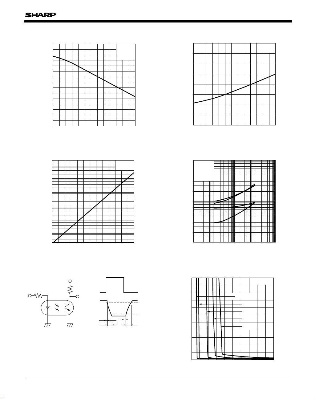
Fig.13 Test Circuit For Response Time
V
CC
R
L
Output
Input
Output
t
d
t
r
t
t
Input
R
D
Fig.14 Collector-emitter Saturation Voltage
vs. Forward Current
=0.5mA
I
C
F
Ta=25°C
1mA
3mA
5mA
7mA
(mA)
10
10%
90%
s
f
8
6
(sat) (V)
CE
V
4
2
Collector-emitter saturation voltage
0
0 2 4 6 8 10
Forward current I

Fig.5 Reflow Soldering
Only one time soldering is recommended within the temperature
profile shown below.
230°C
200°C
180°C
PC3H4/PC3Q64Q
25°C
2min
30s
1min
1.5min
■ Precautions for Use
Please refer to the chapter "Precautions for Use".
1min
 Loading...