


‘REPARED BY: DATE
1. This specification sheets include the contents under the copyright of
Sharp Corporation (“Sharp”). Please keep them with reasonable care as
important information.
them \;i’thout Sharp’s consent,
SPEC No.
PILE No.
SHARP
ELECTRONIC COMPONENTS CROUP
SHARP CORPORATION
SPECIFICATION
Please don’t reproduce or cause anyone reproduce
ISSUE
PACE
REPRESENTATIVE DIVISION
0 PHOTOVOLTAICS DIV.
baOPTO-ELECTRONIC DEVICES DI’
0 ELECTRONIC COMPONENTS DIV.
0
0
ED-93032
April 9, 1993
12 Pages
2.
?lease obey the instructions mentioned below for actual use of this device.
( :; This device is designed for general electronic equipment.
Main uses of this device are as follows;
. Computer
* Measuring equipment
* Home appliance, etc.
c
(2) Please take proper steps in order to maintain reliabflity and safety,
in case this device is used for the uses mentioned belov which require
high reliability.
-Unit concerning control and safety of a vehicle (air plane, train,
automobile etc.)
*Fire box and burglar alarm box
[
0) Please don’t use for the uses mentioned below which require
extremely high reliability
element), etc.
0 CUSTC.LIER’S APPROVAL
l
OA equipment -Telecommunication equipment (Terminal)
*Tooling machine .AV equipment
*Gas leak detection breaker
*Other safety equipment, etc.
.Telecommunication equipment (Trunk)
. Medical equipment (relating to any fatal
PRESENTED
BY
* Traffic signal
I
3
1
DATE
T. Fla tsrimura ,
Department General Manager of
Engineering Dept., TI
Opto-Electronic Devices Div.
ELECOM Group
SHARP CORPORATION BY

1.
Application
This specification applies to the outline and characteristics of
photocoupler Model No. PC3Q64.
2.
Outline
Refer to the attached drawing No. CY5888K02.
3. Ratings and characteristics
3.1 Absolute maximum ratings
PAGE
Ta=25'C
1
*l Forward current
, Input
1
I I
!Output
,
I
*2 Peak forward current
*l Power dissipation
*l Collector power dissipation PC I 150
*l Total power dissipation
Parameter Symbol Rating j Unit
IF /
IFM
! p i
!
Collector-emitter voltage
Emitter-collector voltage
Collector current
Operating temperature
VCEO 1
VECO 1
Ic
I
+50 ; mA
i
I
21
70
35
6
50 ;mt;
1
A I
!
j mW
I
1
V
i vi
, i
! mW i
I
(
I
*1 The derating factors of absolute maximum rating due to ambient
temperature are shown in Fig. 1 'L 4.
*2 Pulse width 5 lOOps, Cuty ratio : 0.001 (Refer to Fig. 5)
*3 AC for 1 min., 40 "u 60%RH, f=60Hz
*4 For 10 s
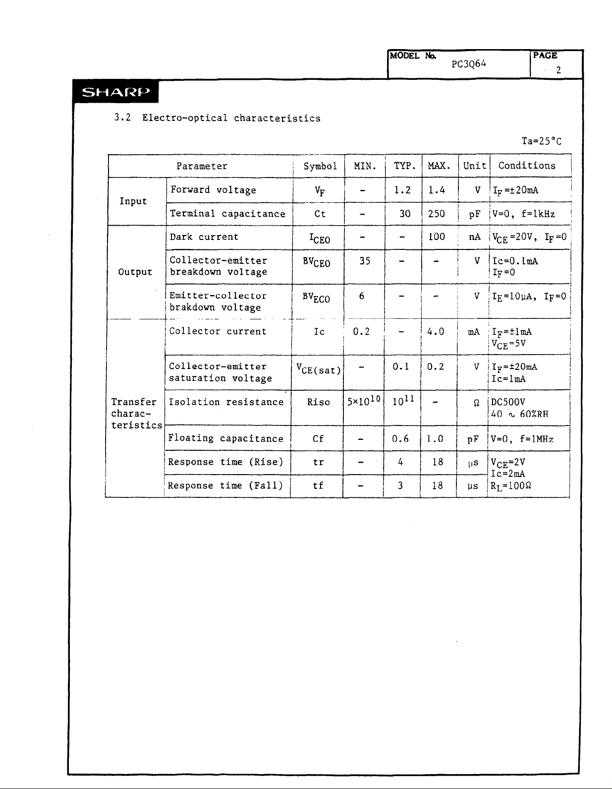
3.2 Electra-optical characteristics
Ta=25"C
Input
output
Transfer
characteristics
Parameter
Forward voltage
Terminal capacitance
Dark current
Collector-emitter
breakdown voltage
Emitter-collector / BVECO 1 6 brakdown voltage
Collector current 1 Ic
Collector-emitter
saturation voltage
j Symbol MIN. ' TYP.
/
"F -
___-._./
j ct - I 1 30 j 250 i pF $=O, f=lkHz j
'CEO
BVCEO
i- /-
I
35 - - 1 v /Ic=O.lmA
I
I
/
0.2 j - ] 4.0 / d &=tld
I
'"CE(sat)
i- 1
1
j
1.2 1.4 : " 'IF='2Oti
0.1 j 0.2 / " i1F=+20ti
MAX. 1 Unit/ Conditions /
f
I
1 100
; d &E=20", IF=0
,
I j IF=0
1 - ; " ;I~=l@ki, IF=0 1
/ ;
j
I
I
/"CE=5" ;
! ' /Ic=lmA
1
Isolation resistance Riso 5x10¹⁰ loll / - 1 $rj iDC500V
/40 ?r 60%RH
I
Ic=2mA
I
Floating capacitance i Cf -
I / 1
Response time (Rise)
tr -
Response time (Fall) 1 tf
I
0.6
I
' 4
- 1 3
I
1
1.0 i pF fV=O, f=lMHz
1 18 j ,,s VCE=2V
I
j 18 1 / , us lRL=lOOO
I
I
I
I
1
1
I
/
i
I

IMODEL No.
I
4. Reliability
Refer to the attached sheet, Page 7.
5. Incoming inspection
Refer to the attached sheet, Page 8.
6. Supplements
6.1 Isolation voltage shall be measured in the following method.
(1) Short between anode and cathode on the primary side and
between collector and Emitter on the secondary side.
(2) The dielectric withstand tester with zero-cross circuit shall
be used,
pc3Q64
(PAGE
I
3
(3) The waveform of applied voltage shall be a sine wave.
(It is recommended that the isolation voltage be measured
in insulation oil)
6.2 This product is AC input type.
6.3 (I) This product is not designed as radiation hardened.
(2) This product is assembled with electrical input and output.
(3) This product incorporates non coherent light emitting diode.
6.4 Package specifications
Refer to the attached sheet, Page 9 to 11.
6.5 UL : Under preparation

Notes
7.
7.1 For cleaning
* Cleaning conditions:
jh4ODEL No.
I
PC3Q64
1 PAGE
I
.
4
(1) Solvent cleaning:
Solvent te perature 45°C or less
Immersion 3 min. or less
(2) Ultrasonic cleaning:
Affection to device by ultrasonic cleaning has
different affection by cleaning bath size,
ultrasonic power output, cleaning
or device mounting condition etc- If user
carries out ultrasonic cleaning, user should
select fit condition that doesn't occur defect.
* The cleaning shall be carried out with solvent below.
Solvent: Ethyl alcohol, Methyl alcohol, Isopropyl alcohol
Freon TE.TF, Daiflon-solvent S3-E
Please refrain from using Chloro Fluoro Carbon type solvent to clean
devices as much as possible since it is restricted to protect the
ozonosphere. Before you use alternative solvent you are requested
to confirm that it does not damage package resin.
7.2 On mounting
In mounting this device, please perform soldering reflow satisfied
with the conditions indicated in page 12. And please pay attention
not to occur the temperature rising of the package sectionally.
time,
PWB size
8. Others
Any doubt as to this specification shall be determined in good faith
upon mutual consultation of the both parties.

SHARI=
Date code *l
I---
iurr
lax. 0.2 Pin Nos*
-i I 1
connection diagram
PC3Q64 Page 5
and internal
Q
d
l tl
W
I
P C 3 Q.6 4
Epoxy resin
.’
l-t
T
m
d
$1
4
-.-
-cu
d
-
e Q@ @Qa aDQ!J @
Date code is composed of 2-digit number marked according
to DIN standard and the,following weekly code .
First week :1
Second week : 2
Third weed : 3
Fouth week : 4
Fifth, Sixth week : 5
UNIT :l/lmm
PC3Q64
Name Outline Dimensions
rawin
0.
cy5888KO2
1

SHARP
Page 6
Fig. 1 Forward current vs.
ambient temperature
-‘Tr 0
Ambient2~empe~~tu~~ '!'~"(oC)
3 Collector power dissipation
Fig .
-
vs. ambient temperature
.a
Fig. 2 Diode power dissipation
vs. ambient temperature
4
.2 55 75
n
-
Ambitnt fzmperature Ta ("C)
Fig. 4 Total power dissipation
ambient temperature
vs.
100
200
150
100 -
-30
Ambiint ?zrnpe?\tuJ: T'aoo(“C)
5 Peak forward current
VS.
duty ratio
\
\
Pulse width S 100~
Ta = 25C
100 --
50 --
150 1
“l
*
Duty ratio

4. Reliability
The reliability of products shall be satisfied with items listed below.
!
/
Test Items
I
PC3Q64
7
I
Confidence level : 90%, LTPD : 10%/20%
Test Conditions Failure Samples (n)l
Judgement
Defective(C)
] Criteria
j Solderability *l i 23O"C, 5 s
Soldering heat *2 i 260°C, 10 s
Terminal strength
(Bending)
Mechanical shock
' Weight : lNtO.lkgf]
*3 , 1 time/each terminal
I
1 15000m/s2{1500G], 0.5ms
/ 3 times/?X, ?Y, ?Z direction
/
Variable frequency i 100 2, 2000 s 100 Hz/4 min.
vibration
j 4 times/X,Y,Z direction
1 200m/s2t20G]
Temperature
: 1 cycle -40°C Q, +125"C
cycling (30min.) (30min.) j
j 20 cycle test
i
High temp. and high i +85"C, 85%RH, 500h
humidity storage
I
High temp. storage 1 +125"C, lOOOh
Low temp. storage i -4O"C, lOOOh
-
Operation life
/
' Ta=25"C, IF=?5OmA
Ptot=l-/OmW, lOOOh
/
,
I
!
1
; VF > u x 1.2 n=ll, C=O
I
/
CEO ‘, u x 2
j I
I
IC <
L x 0.7
'CE(sat)
n=ll, C=O
n=ll, C=O
1 n=ll, C=O
i
] n=ll, C=O
9
>ux1.2 1
!
i n=22, C=()
!
,
jU: Upper
specification. n=22, C=O
i
limit
I
n=22, C=O
:L: Lower
specification n=22, C=O
/
limit
I
I
n=22, C=O
!
*1 Solder shall adhere at the area of 95% or more of immersed portion of
lead and pin hole or other holes shall not be concentrated on one portion.
*2 The lead pin depth dipped into solder shall be away 0.2mm from the
root of lead pins.
(Refer to the below)
*3 Terminal bending direction is shown below.
Weight :
lNfO.lkgf)

Incoming inspection
5.
5.1 Inspection items
(1) Electrical characteristics
IMODEL rb.
I
PC3Q64
IPAGE
8
I
VFY ICE09 VCE(sat
(2) Aplpearance
5.2 Sampling method and Inspection level
A single sampling plan, normal inspection level II based on
MIL-STD-105D is applied. The AQL according to the inspection
items
Defect 1
Major
defect Unreadable marking ! inspection II j 0.1
Minor Appearance defect except Normal
defect
are shown below.
Inspection item
Electrical characteristics i
the above mensioned. inspection II j 0.4
J, Ic, Riso, Viso
I
1 Inspection level AQL(%)
!
I
1
Normal
I
!
!
I

6.2
Package specifications
MODEL Noa
pc3Q64
PAGE
9
6.2.1
(1)
(2)
(3)
(4)
(5)
Taping conditions (Refer to the attached sheet, Page 10)
Tape structure and Dimensions
The tape shall have a structure in which a cover tape is sealed heat-
pressed on the carrier tape of hard vinylchloride to protect against
static electricity.
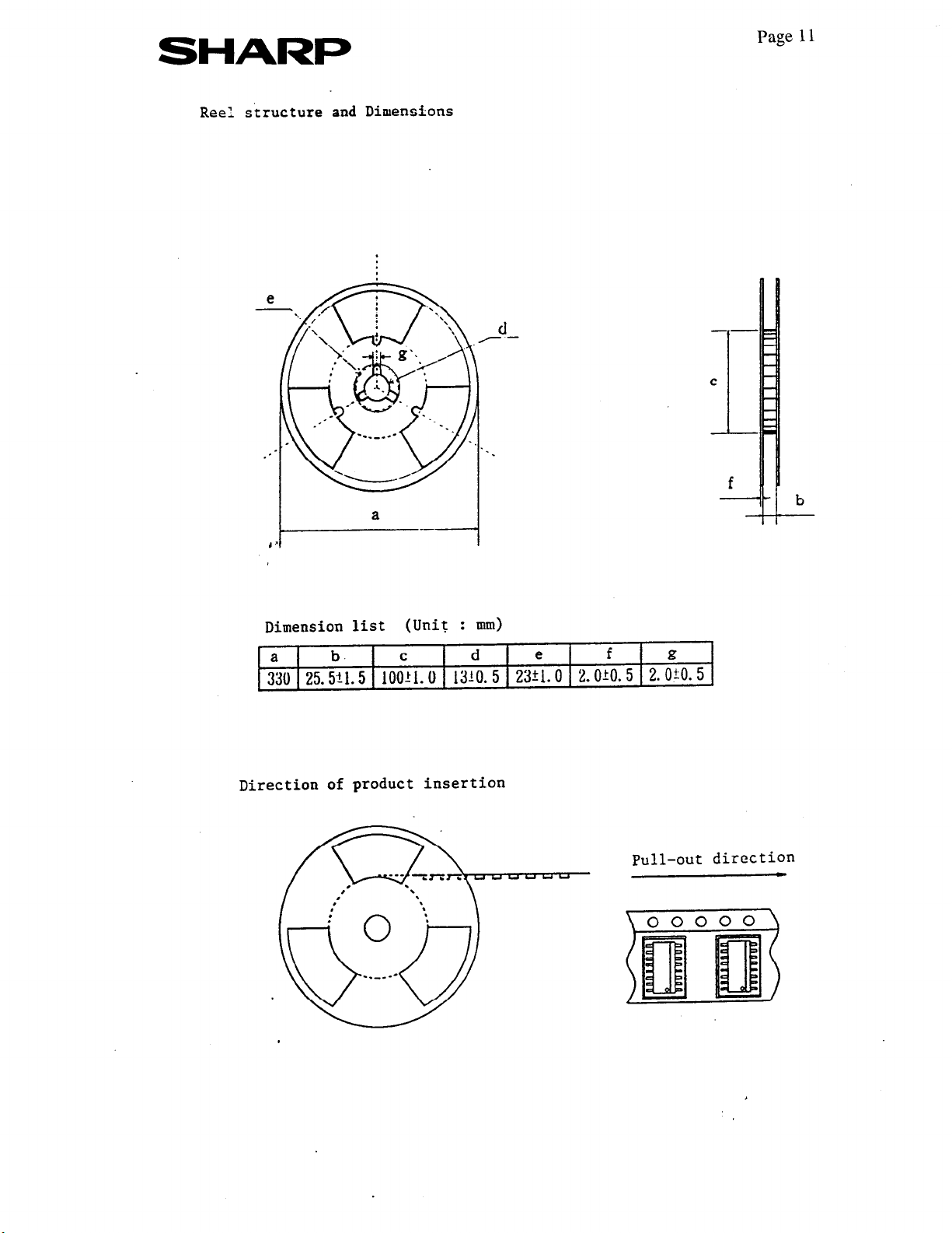
Reel structure and Dimensions (Refer to the attached sheet, Page 11)
The taping reel shall be of corrugated cardboard with its dimensions
as shown in the attached drawing.
Direction of product insertion (Refer to the attached sheet, Page 11)
Product direction in carrier tape shall direct to the anode mark at
the hole side on the tape.
Joint of tape
The cover tape and carrier tape in one reel sha
The way to repair taped failure devices
The way to repair tap’ed failure devices cut a bottom of carrier tape
with a cutter,
shall be sealed with adhesive tape.
and after replacing to good devices, the cutting portion
11 be joint less.
4
6.2.2
6.2.3
6.2.4
6 - -2.3
6.2.6
Adhesiveness of cover tape
The exfoliation force between carrier tape and cover tape shall be
0.2Ni20gf)s lN{lOOgf]for the angle from 160” to 180”.
Rolling method and quanfity
Wind the tape back on the reel so that the cover tape will be outside
the tape.
leader of the tape and fix the both ends with adh sive tape.
One reel shall contain 1000
Marking
The outer packaging case shall be marked with following information.
* Model No. * Number of pieces delivered
Storage condition
Taped procuts shall be stored at the tempera ure lower than
5 ‘L 30°C and the humidities lower than 70ZRH.
Safety protection during shipping
There shall be no deformation of component or degradation of electrical
characteristecs due to shipping.
Attach more than 20cm of blank tape to the trailer and the
PCS.
* Production date

SHARI=
Tape structure and Dimensions
Page
10
I
-
Dimension list
1 A i C t D
I 24. oto. 3 I 11. 5?0. 1 I 1.75+0. 1
1 0.4io. 05
I 3. oio. 1
(Unit :‘mm)
I
7.4iO.l
5” max
E F
12.OYJ.l 2.0+0.1 4.WO.I )1.5’>’ LO. 8+-O. 1
G
Ii I
SHARI=
Reel structure and DimensTons
Page 11
Dimension list (Unit : mm)
a b.
330 25.5Al.5 lO;!l. 0 1310. 5 23:l. 0 2.010.5 2. Ok 5
Direction of product insertion
d
f
Pull-out direction

Precautions for Soldering Photocouplers
I. If solder reflow:
MODEL I’b. PAGE
PC3Q64 12
It is recommended that only one
temperature and the time within
shown in the figure.
,
L--
2 min.
--__-_-- --; ,
Ii37 c
*
!
'1.5 min.
soldering be done at the
the temperature profile as
i;
1 min.
1
‘!
1 min:' i
Other precautions
2.
An infrared lamp used to heat up for soldering may cause a
localized temperature rise in the resin. So keep the package
temperature within that specified in Item 1.
Also avoid immersing
the resin part in the solder.
 Loading...