

Sharp LH28F800BVHE-BTL90 Datasheet

®
PRODUCT SPECIFICATIONS
Integrated Circuits Group
LH28F800BVHE-BTL90
Flash Memory
8M (1M ×8/512K x 16)
(Model No.: LHF80V13)
Spec No.: EL109049A
Issue Date: December 1, 1998
SHARP
LHFSOV13
l Handle this document carefully for it contains material protected by international copyright law.
Any reproduction, full or in part, of this material is prohibited without the express written
permission of the company.
l When using the products covered herein, please observe the conditions written herein and the
precautions outlined in the following paragraphs. In no event shall the company be liable for any
damages resulting from failure to strictly adhere to these conditions and precautions.
(1) The products covered herein are designed and manufactured for the following application
areas. When using the products covered herein for the equipment listed in Paragraph (2),
even for the following application areas, be sure to observe the precautions given in
Paragraph (2). Never use the products for the equipment listed in Paragraph (3).
*Office electronics
*Instrumentation and measuring equipment
*Machine tools
*Audiovisual equipment
*Home appliance
l Communication equipment other than for trunk lines
(2) Those contemplating using the products covered herein for the following equipment which
demands high reliabilitv, should first contact a sales representative of the company and then
accept responsibility for incorporating into the design fail-safe operation, redundancy, and
other appropriate measures for ensuring reliability and safety of the equipment and the
overall system.
*Control and safety devices for airplanes, trains, automobiles, and other
transportation equipment
*Mainframe computers
@Traffic control systems
@Gas leak detectors and automatic cutoff devices
*Rescue and security equipment
*Other safety devices and safety equipment, etc.
(3) Do not use the products covered herein for the following equipment which demands
extremelv high performance in terms of functionality, reliability, or accuracy.
*Aerospace equipment
l Communications equipment for trunk lines
*Control equipment for the nuclear power industry
l Medical equipment related to life support, etc.
(4) Please direct all queries and comments regarding the interpretation of the above three
Paragraphs to a sales representative of the company.
aPlease direct all queries regarding the products covered herein to a sales representative of the
company.
Rev. 1.01
SHARP
LHF8OVl3
CONTENTS
PAGE
1 INTRODUCTION..
1.1 Features
1.2 Product Overview.
2 PRINCIPLES OF OPERATION.. .....................................
2.1 Data Protection.. ...........................................................
3,BUS OPERATION ...........................................................
3.1 Read
3.2 Output Disable.. ............................................................
3.3 Standby.. .......................................................................
3.4 Deep Power-Down ......................................................
3.5 Read Identifier Codes Operation.. ...............................
3.6 Write .............................................................................
4 COMMAXD DEFINITIONS..
4.1 Read Array Command
4.2 Read Identifier Codes Command ............................... 12
4.3 Read Status Register Command..
4.4 Clear Status Register Command.. ............................... 12
4.5 Block Erase Command.
4.6 Word/Byte Write
4.7 Block Erase Suspend Command ................................
4.8 Word/Byte Write Suspend Command..
4.9 Considerations of Suspend ......................................... 14
4.10 Block Locking
.............................................................................. 8
4.10.1 V,,=V,, for Complete Protection.. .................... 14
4.10.2 WP#=V,, for Block Locking.. ............................ 14
4.10.3 WP#=V,, for Block Unlocking.. ........................ 14
............................................................ 3
........................................................................ 3
........................................................ 3
.7
8
.8
8
8
.8
.9
9
..........................................
................................................ 12
............................... 12
..............................................
Command.. ..................................... 13
...................... 14
.......................................................... 14
.9
12
13
PAGE
5 DESIGN CONSIDERATIONS ...................................... 20
5.1 Three-Line Output Control
5.2 RY/BY# and Block Erase and Word/Byte Write
Polling.. .................................................................... 20
5.3 Power Supply Decoupling ........................................
5.4 V,, Trace on Printed Circuit Boards ........................ 20
5.5 V,,, V,, RP## Transitions..
5.6 Power-Up/Down Protection..
5.7 Power Dissipation
6 ELECTRICAL SPECIFICATIONS ............................... 22
6.1 Absolute Maximum Ratings ..................................... 22
6.2 Operating Conditions ................................................
6.2.1 Capacitance
6.2.2 AC Input/Output Test Conditions
6.2.3 DC Characteristics .............................................. 24
6.2.4 AC Characteristics - Read-Only Operations..
6.2.5 AC Characteristics - Write Operations
6.2.6 Alternative CE#-Controlled Writes.. ................... 3 1
6.2.7 Reset Operations ................................................. 33
6.2.8 Block Erase and Word/Byte Write Performance 34
7 PACKAGE AND PACKING SPECIFICATIONS.. ......
..................................................... 21
......................................................... 22
....................................... 20
20
..................................... 21
.................................... 21
22
....................... 23
..... 26
............... 29
.35
1
Rev. 1.0
SHARP
LH28F8OOBVHE-BTL90
8M-BIT (1Mbit x 8 / 512Kbit x 16)
Smart3 Flash MEMORY
n Smart3 Technology
- 2.7V-3.6V Vcc
-
2.7V-3.6V or 11.4V-12.6V Vpp
n User-Configurable x8 or x 16 Operation
n High-Performance Access Time
- 90ns(2.7V-3.6V)
n Operating Temperature
- -40°C to +85”C
n Optimized Array Blocking Architecture
-
Two 4k-word Boot Blocks
- Six 4k-word Parameter Blocks
-
Fifteen 32k-word Main Blocks
- Bottom Boot Location
n Extended Cycling Capability
-
100,000 Block Erase Cycles
n Enhanced Automated Suspend Options
-
Word/Byte Write Suspend to Read
-
Block Erase Suspend to Word/Byte Write
-
Block Erase Suspend to Read
LHF8OV13
n Enhanced Data Protection Features
n Automated Word/Byte Write and Block Erase
n Low Power Management
n SRAM-Compatible Write Interface
n Industry-Standard Packaging
n ETOXTM” Nonvolatile Flash Technology
n CMOS Process (P-type silicon substrate)
w Not designed or rated as radiation hardened
-
Absolute Protection with Vpp=GND
-
Block Erase and Word/Byte Write Lockout
during Power Transitions
-
Boot Blocks Protection with WP#=VIL
-
Command User Interface
- Status Register
-
Deep Power-Down Mode
-
Automatic Power Savings Mode Decreases
ICC in Static Mode
- 48-Lead TSOP
2
SHARP’s LH28F800BVHE-BTL90 Flash memory with Smart3 technology is a high-density, low-cost, nonvolatile, read/write
storage solution for a wide range of applications. LH28F800BVHE-BTL90 can operate at V,,=2.7V-3.6V and
V,=2.7V-3.6V. Its low voltage operation capability realize battery life and suits for cellular phone application.
[ts Boot, Parameter and Main-blocked architecture, flexible voltage and extended cycling provide for highly flexible
component suitable for portable terminals and personal computers. Its enhanced suspend capabilities provide for an ideal
solution for code + data storage applications. For secure code storage applications, such as networking, where code is either
directly executed out of flash or downloaded to DRAM, the LH28F800BVHE-BTL90 offers two levels of protection: absolute
protection with V,, at GND, selective hardware boot block locking. These alternatives give designers ultimate control of their
code security needs.
Ihe LH28F800BVHE-BTL90 is manufactured on SHARP’s 0.35pm ETOXTM* process technology. It come in industrystandard package: the 48-lead TSOP ideal for board constrained applications.
*ETOX is a trademark of Intel Corporation.
Rev. 1.01

SHARP
LHF8OV13
1 INTRODUCTION
This datasheet contains LH28F8OOBVHE-BTL90
specifications. Section 1 provides a flash memory
overview. Sections 2,3,4 and 5 describe the memory
organization and functionality. Section 6 covers electrical
specifications.
1.1 Features
Key enhancements of LH28F800BVHE-BTL90 Smart3
Flash memory are:
*Smart3 Technology
*Enhanced Suspend Capabilities
*Boot Block Architecture
Please note following important differences:
l
VPPLK has been lowered to 1.5V to support 2.7V-3.6V
block erase and word/byte write operations. The V,
voltage transitions to GND is recommended for
designs that switch V,, off during read operation.
*To take advantage of Smart3 technology, allow V,,
and V,,, connection to 2.7V-3.6V.
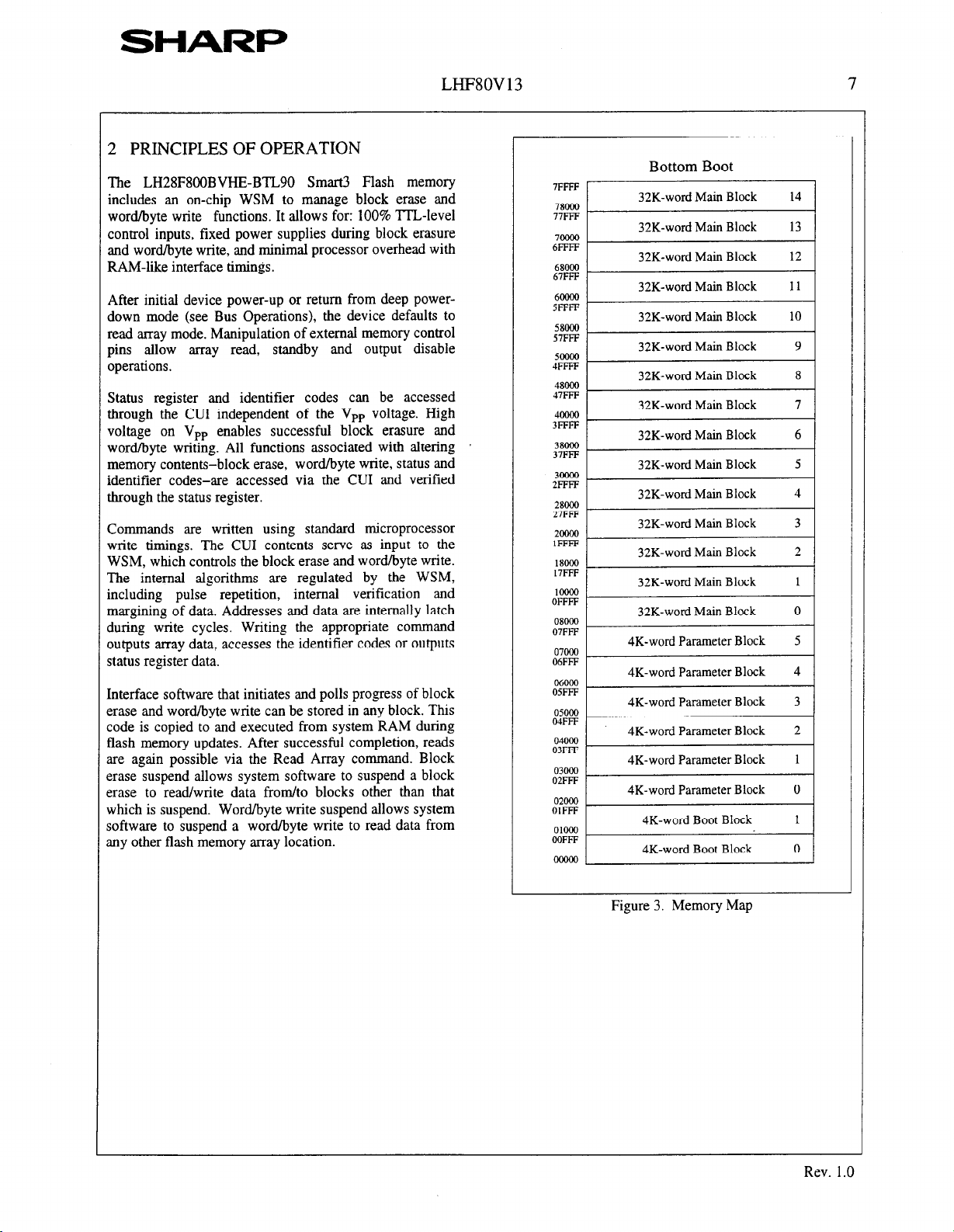
1.2 Product Overview
The LH28F800BVHE-BTL90 is a high-performance 8Mbit Smart3 Flash memory organized as lM-byte of 8
bits or 512K-word of 16 bits. The lM-byte/512K-word of
data is arranged in two 8K-byte/4K-word boot blocks, six
8K-byte/4K-word parameter blocks and fifteen 64Kbyte/32K-word main blocks which are individually
erasable in-system. The memory map is shown in Figure
3.
Smart3 technology provides a choice of V,, and V,,
combinations, as shown in Table 1, to meet system
performance
and
power expectations. V, at 2.7V-3.6V
3
eliminates the need for a separate 12V converter, while
V,=l2V maximizes block erase and word/byte wriu
performance. In addition to flexible erase and prograrr
voltages, the dedicated V,, pin gives complete datr
protection when V,, 5 VPPLK.
Table 1. V,, and V,, Voltage Combinations Offered by
Smart3 Technology
V,, Voltage V,, Voltage
2.7V-3.6V
Internal V,, and V,
configures the device for optimized read and write
operations.
A Command User Interface (CUI) serves as the interface
between the system processor and internal operation of the
device. A valid command sequence written to the CUI
initiates device automation. An internal Write State
Machine (WSM) automatically executes the algorithms
and timings necessary for block erase and word/byte write
operations.
A block erase operation erases one of the device’s 32Kword blocks typically within 0.51s (2.7V-3.6V V,,,
11.4V-12.6V V,,), 4K-word blocks typically within 0.3 1 s
(2.7V-3.6V V,,, 11.4V- 12.6V V,,) independent of other
blocks. Each block can be independently erased 100,000
times. Block erase suspend mode allows system software
to suspend block erase to read or write data from any other
block.
Writing memory data is performed in word/byte
increments of the device’s 32K-word blocks typically
within 12.6~s (2.7V-3.6V V,,, 11.4V-12.6V V,,), 4Kword blocks typically within 24.5us (2.7V-3.6V V,,,
11.4V-12.6V V,,). Word/byte write suspend mode
enables the system to read data or execute code from any
other flash memory array location.
2.7V-3.6V, 11.4V- 12.6V ~
detection Circuitry automatically
Rev. 1.1
LHF8OV13
The boot blocks can be locked for the WP# pin. Block
erase or word/byte write for boot block must not be carried
out by WP# to Low and RP# to V,
The status register indicates when the WSM’s block erase
or word/byte write operation is finished.
The RY/BY# output gives an additional indicator of WSM
activity by providing both a hardware signal of status
(versus software polling) and status masking (interrupt
masking for background block erase, for example). Status
polling using RY/BY# minimizes both CPU overhead and
system power consumption. When low, RY/BY# indicates
that the WSM is performing a block erase or word/byte
write. RY/BY#-high Z indicates that the WSM is ready for
a new command, block erase is suspended (and word/byte
write is inactive), word/byte write is suspended, or the
device is in deep power-down mode.
The access time is 90 ns
temperature range (-40°C to +8 80 C) and V,, supply
voltage range of 2.lV-3.6V.
(tAv v> over the extended
The Automatic Power Savings (APS) feature substantially
reduces active current when the device is in static modt
(addresses not switching). In APS mode, the typical I,,
current is 3 mA at 2.7V V,,.
When CE# and RP# pins are at V,,, the I,, CM05
standby mode is enabled. When the RP# pin is at GND
deep power-down mode is enabled which minimize:
power consumption and provides write protection during
reset. A reset time (tpHQv) is required from RP# switching
high until outputs are valid. Likewise, the device has :
wake time (tp&
are recognized. With RP# at GND, the WSM is reset ant
the status register is cleared.
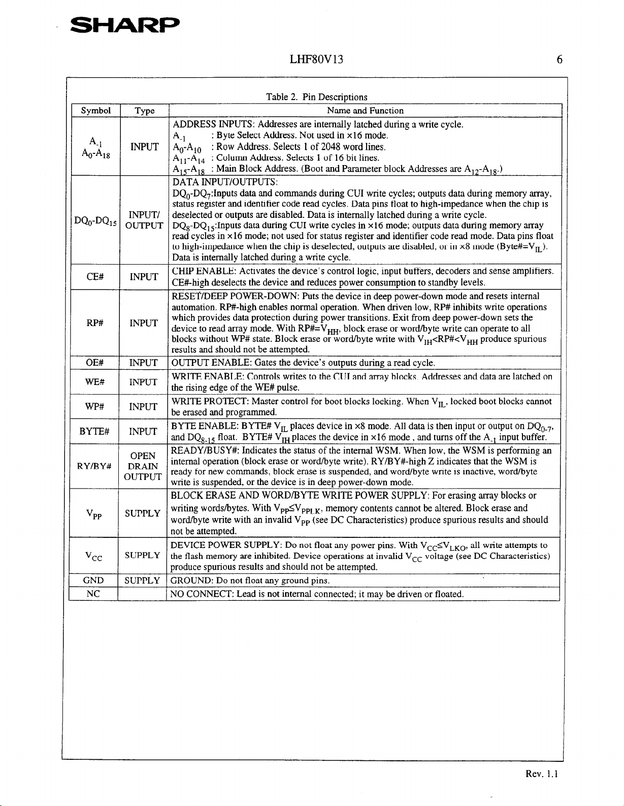
The device is available in 48-lead TSOP (Thin Small
Outline Package, 1.2 mm thick). Pinout is shown in Figure
2.
from RP#-high until writes to the CUI
Rev. 1.0
SHARP
Y
1 Decoder
LHF8OV13
Y-Gating
I
I Write I
a3
WE#
OE#
RP#
WP#
) RYiBY#
5
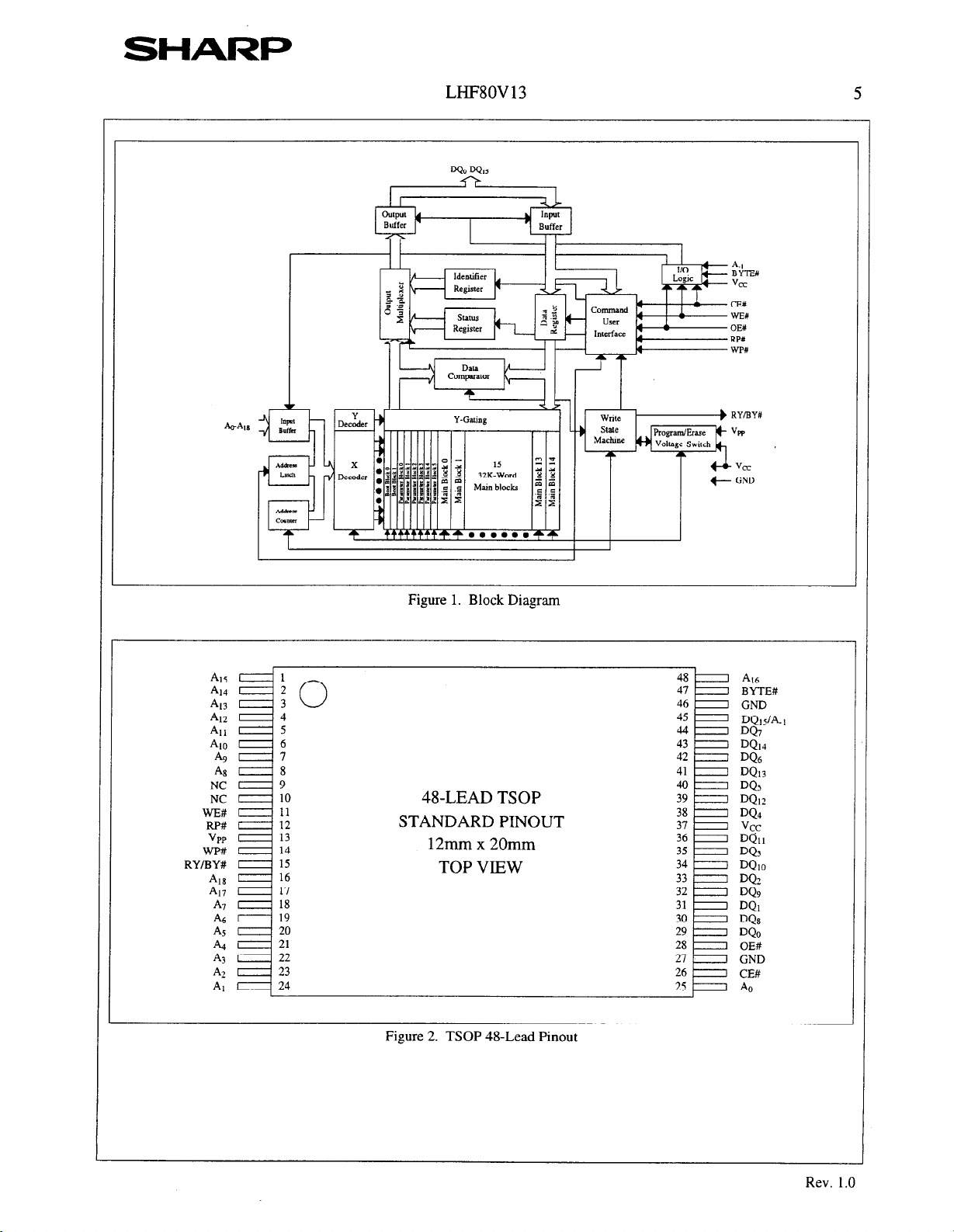
Figure 1. Block Diagram
AIS c== 1
A14 I 2 47 BYTE#
A13 I 3
A12 : 4 45
41 15 44
ho :
A9 = 7 42
As I 8 41
NC I 9
NC 10
wE# 11
RP# 12
VPP 13
WP# 14
RYIBY# 1.5
48
A17 17 32
A7 18 31
% 19 30
2 20 21 28 29
A3 I 22
A2 I 23
A, I 24
0
6
48-LEAD TSOP
STANDARD PINOUT
12mm x 20mm
16 33 DQ2
TOP VIEW
48 A16
46 GND
43
a
40
39
38
37
36
35
34
21
I GND
26
I CE#
25 I A0
Figure 2. TSOP 48-Lead Pinout
DQdAI
DQ7
DQM
DQ6
DQI~
DQs
DQIZ
DQ4
VCC
DQI
DQ3
DQIO
DQg
DQ1
DQs
DQo
OE#
Rev. 1.0
SHARP
Symbol
A-1
Ao-Al 8
DQu-DQls
CE#
RP#
OE#
WE#
WP# INPUT
BYTE# INPUT
RY/BY# DRAIN
VPP
Vcc
GND
NC
‘Me
INPUT Au-A ,u : Row Address. Selects 1 of 2048 word lines.
INPUT/ deselected or outputs are disabled. Data is internally latched during a write cycle.
OUTPUT
INPUT CHIP ENABLE: Activates the device’s control logic, input buffers, decoders and sense amplifiers.
INPUT
INPUT
INPUT
OPEN
OUTPUT
SUPPLY
SUPPLY the flash memory are inhibited. Device operations at invalid V,, voltage (see DC Characteristics)
SUPPLY
LHF8OV13
Table 2. Pin Descriptions
Name and Function
ADDRESS INPUTS: Addresses are internally latched during a write cycle.
A-1
A,,-A,, : Column Address. Selects 1 of 16 bit lines.
A,5-A,8 : Main Block Address. (Boot and Parameter block Addresses are A,2-A,8.)
DATA INPUT/OUTPUTS :
DQo-DQ7:Inputs data and commands during CUI write cycles; outputs data during memory array,
status register and identifier code read cycles. Data pins float to high-impedance when the chip is
DQs-DQrs:Inputs data during CUI write cycles in x16 mode; outputs data during memory array
read cycles in x 16 mode; not used for status register and identifier code read mode. Data pins float
to high-impedance when the chip is deselected, outputs are disabled, or in x8 mode (Byte#=V,,).
Data is internally latched during a write cycle.
CE#-high deselects the device and reduces power consumption to standby levels.
RESET/DEEP POWER-DOWN: Puts the device in deep power-down mode and resets internal
automation. RP#/-high enables normal operation. When driven low, RP# inhibits write operations
which provides data protection during power transitions. Exit from deep power-down sets the
device to read array mode. With RP#=V HH, block erase or word/byte write can operate to all
blocks without WP## state. Block erase or word/byte write with V,,<RP#<VHH produce spurious
results and should not be attempted.
OUTPUT ENABLE: Gates the device’s outputs during a read cycle.
WRITE ENABLE: Controls writes to the CUI and array blocks. Addresses and data are latched on
the rising edge of the WE# pulse.
WRITE PROTECT: Master control for boot blocks locking. When VI,. locked boot blocks cannot
be erased and programmed.
BYTE ENABLE: BYTE# V,, places device in x8 mode. All data is then input or output on DQ,-,,
and DQ8-15 float. BYTE# VIH places the device in x16 mode , and turns off the A-, input buffer.
READY/BUSY#: Indicates the status of the internal WSM. When low, the WSM is performing an
internal operation (block erase or word/byte write). RY/BY#-high Z indicates that the WSM is
ready for new commands, block erase is suspended, and word/byte write is inactive, word/byte
write is suspended, or the device is in deep power-down mode.
BLOCK ERASE AND WORD/BYTE WRITE POWER SUPPLY: For erasing array blocks or
writing words/bytes. With V,,<V,,,,, memory contents cannot be altered. Block erase and
word/byte write with an invalid V,, (see DC Characteristics) produce spurious results and should
not be attempted.
DEVICE POWER SUPPLY:
produce spurious results and should not be attempted.
GROUND: Do not float any ground pins.
NO CONNECT: Lead is not internal connected; it may be driven or floated.
: Byte Select Address. Not used in x16 mode.
Do not float any power pins.
With VcclV,KO, all write attempts to
Rev. 1.1
SHARP
LHF8OV13 7
2 PRINCIPLES OF OPERATION
The LH28F8OOBVHE-BTL90 Smart3 Flash memory
includes an on-chip WSM to manage block erase and
word/byte write functions. It allows for: 100% TTL-level
control inputs, fixed power supplies during block erasure
and word/byte write, and minimal processor overhead with
RAM-like interface timings.
After initial device power-up or return from deep powerdown mode (see Bus Operations), the device defaults to
read array mode. Manipulation of external memory control
pins allow array read, standby and output disable
operations.
Status register and identifier codes can be accessed
through the CUI independent of the VP, voltage. High
voltage on VP,
word/byte writing. All functions associated with altering
memory contents-block erase, word/byte write, status and
identifier codes-are accessed via the CUI and verified
through the status register.
Commands are written using standard microprocessor
write timings. The CUI contents serve as input to the
WSM, which controls the block erase and word/byte write.
The internal algorithms are regulated by the WSM,
including pulse repetition, internal verification and
margining of data. Addresses and data are internally latch
during write cycles. Writing the appropriate command
outputs array data, accesses the identifier codes or outputs
status register data.
enables successful block erasure and
7FFFF
78000
77FFF
7maO
6FFFF
68000
67FFF
58OCO
57FFF
48OCQ
47FFF
28000
27FFF
2OOa
1FFFF
18000
17FFF
08000
07FFF
07OQO
06FFF
Bottom
Boot
Interface software that initiates and polls progress of block
erase and word/byte write can be stored in any block. This
code is copied to and executed from system RAM during
flash memory updates. After successful completion, reads
are again possible via the Read Array command. Block
erase suspend allows system software to suspend a block
erase to read/write data from/to blocks other than that
which is suspend. Word/byte write suspend allows system
software to suspend a word/byte write to read data from
any other flash memory array location.
0%
05000
04FFF
04000
03FFF
03000
02FFF
02Om
OIFFF
OloOa
OOFFF
omoo
4K-word Parameter Block
4K-word Parameter Block
4K-word Parameter Block 0
4K-word Boot Block 1
4K-word Boot Block
Figure 3. Memory Map
2
1
0
Rev. 1.0
SHARI=
LHF8OV13 8
2.1 Data Protection
Depending on the application, the system designer may
choose to make the V, power supply switchable
(available only when memory block erases or word/byte
writes are required) or hardwired to V,,,,,. The device
accommodates either design practice and encourages
optimization of the processor-memory interface.
When VppIVppLK,
The CUI, with two-step block erase or word/byte write
command sequences, provides protection from unwanted
operations even when high voltage is applied to V,,. All
write functions are disabled when V,, is below the write
lockout voltage VLKO
boot blocks locking capability for WP# provides
additional protection from inadvertent code or data
alteration by block erase and word/byte write operations.
Refer to Table 6 for write protection alternatives.
memory contents cannot be altered.
or when RP# is at V,,. The device’s
3 BUS OPERATION
The local CPU reads and writes flash memory in-system.
All bus cycles to or from the flash memory conform to
standard microprocessor bus cycles.
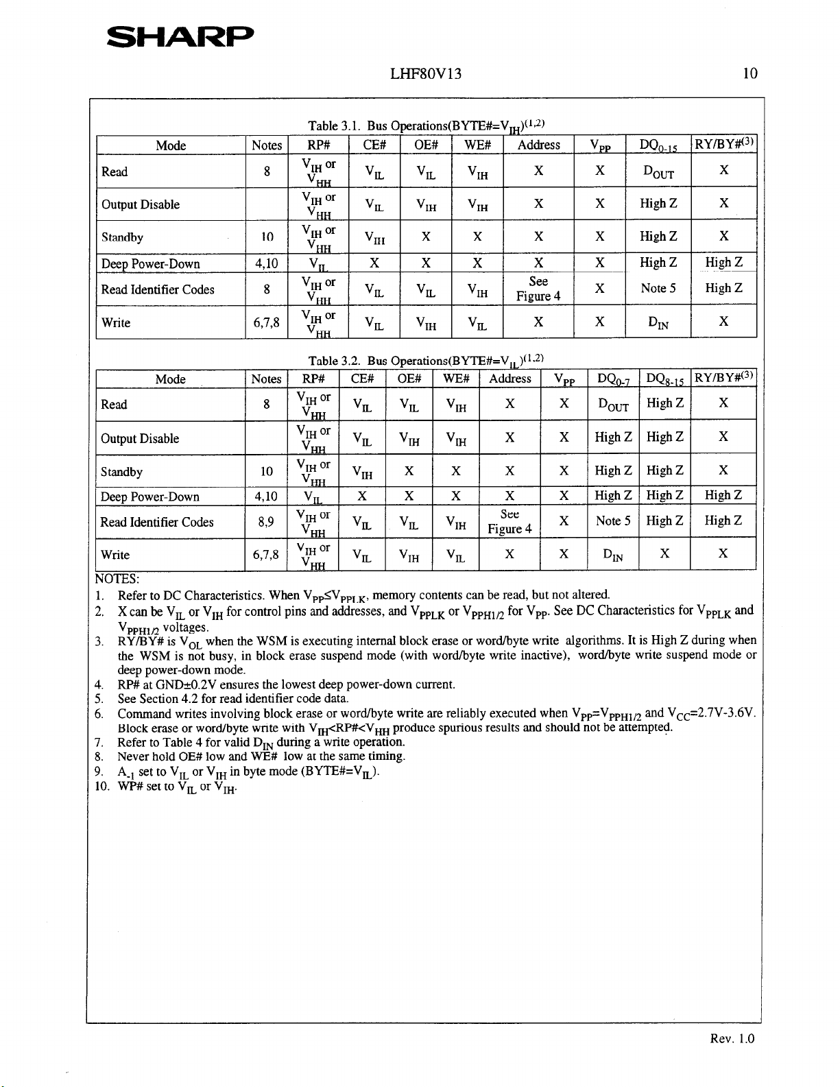
3.1 Read
Information can be read from any block, identifier codes
or status register independent of the V,, voltage. RP# can
be at either VI, or V,.
The first task is to write the appropriate read mode
command (Read Array, Read Identifier Codes or Read
Status Register) to the CUI. Upon initial device power-up
or after exit from deep power-down mode, the device
automatically resets to read array mode. Six control pins
dictate the data flow in and out of the component: CE#,
OE#, WE#, RP#, WP# and BYTE#. CE# and OE# must be
driven active to obtain data at the outputs. CE# is the
device selection control, and when active enables the
selected memory device. OE# is the data output
(DQo-DQls) control and when active drives the selected
memory data onto the I/O bus. WE# must be at Vt, and
RP# must be at V,, or V,,. Figure 11, 12 illustrates read
cycle.
3.2 Output Disable
With OE# at a logic-high level (V,,), the device output
are disabled. Output pins (DQu-DQ15) are placed in a
high-impedance state.
3.3 Standby
CE# at a logic-high level (V,,) places the device in
standby mode which substantially reduces device power
consumption. DQo-DQ,, outputs are placed in a highimpedance state independent of OE#. If deselected during
block erase or word/byte write, the device continues
functioning, and consuming active power until the
operation completes.
3.4 Deep Power-Down
RP# at V, initiates the deep power-down mode.
In read modes, RP#-low deselects the memory, places
output drivers in a high-impedance state and turns off all
internal circuits. RP# must be held low for a minimum 01
100 ns. Time tpHQv is required after return from powerdown until initial memory access outputs are valid. After
this wake-up interval, normal operation is restored. The
CUI is reset to read array mode and status register is set to
80H.
During block erase or word/byte write modes, RP#-low
will abort the operation. RY/BY# remains low until the
reset operation is complete. Memory contents being
altered are no longer valid; the data may be partially
erased or written. Time tpHWL is required after RP# goes
to logic-high (V,,) before another command can be
written.
As with any automated device, it is important to assert
RP# during system reset. When the system comes out of
reset, it expects to read from the flash memory. Automated
flash memories provide status information when accessed
during block erase or word/byte write modes. If a CPU
reset occurs with no flash memory reset, proper CPU
initialization may not occur because the flash memory
may be providing status information instead of array data.
SHARP’s flash memories allow proper CPU initialization
following a system reset through the use of the RP# input.
In this application, RP# is controlled by the same RESET#
signal that resets the system CPU.
Rev. 1.0
SHARI=
LHF8OV13 9
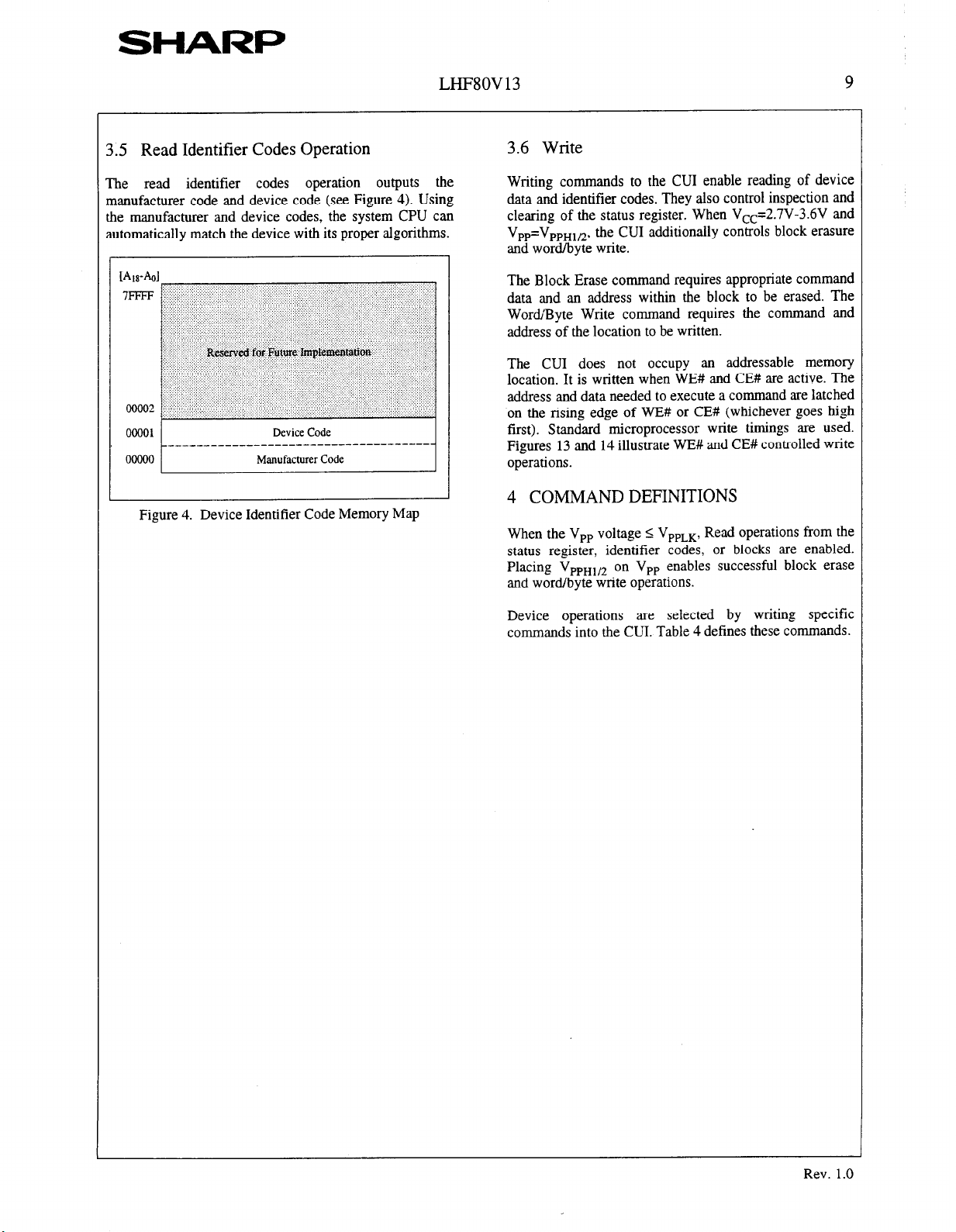
3.5 Read Identifier Codes Operation
The read identifier codes operation outputs the
manufacturer code and device code (see Figure 4). Using
the manufacturer and device codes, the system CPU can
automatically match the device with its proper algorithms.
LGA01
7* :; :, :: .,,,.. ,:’ ,..,:, ::
.I :. ‘; : ..: :,.. . .
..,., :. ., ., .,,, :
. . . .
.:.. ...:’
.:... :,. .I..‘/./.
,. :.:. : ,‘, y:. .;y.:. ,:i,.. ‘,‘.
: .d:.:‘.. ..:..,:,.:,‘j.. . . . . -:,; : ,,,, ,.., :.I.‘.’ .:
Figure 4. Device Identifier Code Memory Map
.f: ‘::,’ ,;’ .:; j, ;:; : ,;., ,,:, :;y)::: j,: .:.: ::,::,,:I ,.., :;‘. $
:
.,..I .,., :, .‘.,,.:, ‘,.,‘j’. :,,, :::,:: ,. . . . . :., ‘:. :; :. :
j ,,,::,,: ,.., ‘. ,:,.
.... ‘. . . .
. . . . ,,
:>:: ,.,. : : .:,. j. .y:: ‘..
.,, :.:.
. . . . . ..A.. .
.ji
. . . .
.
.,,:.,,.
3.6 Write
Writing commands to the CUI enable reading of device
data and identifier codes. They also control inspection and
clearing of the status register. When V,,=2.7V-3.6V and
V,=V,,,,, the CUI additionally controls block erasure
and word/byte write.
The Block Erase command requires appropriate command
data and an address within the block to be erased. The
WordByte Write command requires the command and
address of the location to be written.
The CUI does not occupy an addressable memory
location. It is written when WE# and CE# are active. The
address and data needed to execute a command are latched
‘on the rising edge of WE# or CE# (whichever goes high
first). Standard microprocessor write timings are used.
Figures 13 and 14 illustrate WE# and CE# controlled write
operations.
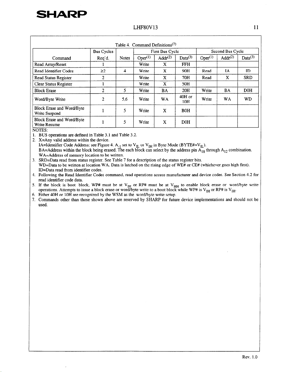
4 COMMAND DEFINITIONS
When the V, voltage I V,,,, Read operations from the
status register, identifier codes, or blocks are enabled.
Placing VPPHIR on V,, enables successful block erase
and word/byte write operations.
Device operations are selected by writing specific
commands into the CUI. Table 4 defines these commands.
Rev. 1.0
SHARP
LHFSOV13 10
Deep Power-Down
Read Identifier Codes
Write
4,lO v, X X X X
8 !$Hor v, v,
I-m
6,7,8 “:” Or V,
HH
VI,
VI, VIL
See
Figure 4
X X
X High Z High Z
X Note 5 High Z
DIN
X
Table 3.2. Bus Operations(BYTE#=Vn.)(*,2)
Mode Notes RP##
Read
Output Disable
Standby
Deep Power-Down
Read Identifier Codes
Write
76-m
IuII2s:
4,lO
6 7 8
vIH Or
8
VHH
‘1, Or
V,
“:” Or
10
8,9 “:” Or V, V,
7 7
HI-l
VI,
HI-l
‘IHor
VI-II-I
. Refer to DC Characteristics. When V,r,5V,PLK,
CE# OE# WE# Address
VIL VIL VIH
VIL
‘1,
vIH vIH
X X X X HighZ High Z X
X X
X X
X X X X
See
vIH
VIL vIH vIL
Figure 4
X X
memory contents can be read, but not altered.
!. X can be Vu or VrB for control pins and addresses, and V,, or V,,,z for V,.
VP,
See DC Characteristics for V,,, and
DQ,-7 DQ,-1, RY/BY#c3)
D,,, High Z X
High Z High Z X
X High Z High Z High Z
X Note 5 High Z
DIN
,
X
High Z
X
vPPHI/2 voltages.
1, RY/BY# is V,, when the WSM is executing internal block erase or word/byte write algorithms. It is High Z during when
the WSM is not busy, in block erase suspend mode (with word/byte write inactive), word/byte write suspend mode or
deep power-down mode.
‘. RP# at GNDk0.2V ensures the lowest deep power-down current.
‘. See Section 4.2 for read identifier code data.
I. Command writes involving block erase or word/byte write are reliably executed when VPP=VPPHrjz and V,--=2.7V-3.6V.
Block erase or word/byte write with VnrcRP#<V, produce spurious results and should not be attempted.
. Refer to Table 4 for valid DIN during a write operation.
Never hold OE# low and WE# low at the same timing.
~1
A-1 set to VI, or VlB in byte mode (BYTE#=Vu).
0. w# set to vL or VI,.
Rev. 1.0
SHARP
LHF8OV13
Table 4. Command Detinitions(7)
NOTES:
1. BUS operations are defined in Table 3.1 and Table 3.2.
2. X=Any valid address within the device.
IA=Identifier Code Address: see Figure 4. A-, set to V, or V,, in Byte Mode (BYTE#=V,).
BA=Address within the block being erased. The each block can select by the address pin A,, through A,, combination.
WA=Address of memory location to be written.
3. SRD=Data read from status register. See Table 7 for a description of the status register bits.
WD=Data to be written at location WA. Data is latched on the rising edge of WE# or CE# (whichever goes high first).
ID=Data read from identifier codes.
4. Following the Read Identifier Codes command, read operations access manufacturer and device codes. See Section 4.2 for
read identifier code data. read identifier code data.
5. If the block is boot block, WP# must be at V, or RP# must be at V,, 5. If the block is boot block, WP# must be at V, or RP# must be at V,,
operations. Attempts to issue a block erase or word/byte write to a boot block while WP# is V,, or RP# is V,,. operations. Attempts to issue a block erase or word/byte write to a boot block while WP# is V,, or RP# is V,,.
6. 6. Either 40H or 10H are recognized by the WSM as the word/byte write setup. Either 40H or 10H are recognized by the WSM as the word/byte write setup.
7. Commands other than those shown above are reserved by SHARP for future device implementations and should not be 7. Commands other than those shown above are reserved by SHARP for future device implementations and should not be
used. used.
to enable block erase or word/byte write to enable block erase or word/byte write
Rev. 1.0
 Loading...