

Page 1

TopPage
LC-37D90U
SERVICE MANUAL
No. S56S8LC37D90U
LCD COLOR TELEVISION
In the interests of user-safety (Required by safety regulations in some countries) the set should
be restored to its original condition and only parts identical to those specified should be used.
CONTENTS
SAFETY PRECAUTION
CHAPTER 1. SPECIFICATIONS
CHAPTER 2. OPERATION MANUAL
CHAPTER 3. DIMENSIONS
CHAPTER 4. REMOVING OF MAJOR PARTS
CHAPTER 5. ADJUSTMENT
CHAPTER 6. TROUBLE SHOOTING TABLE
CHAPTER 7. OVERALL WIRING/BLOCK DIAGRAM
CHAPTER 8. SCHEMATIC DIAGRAM
MODEL
LC-37D90U
CHAPTER 9. PRINTED WIRING BOARD ASSEMBLIES
Parts Guide
Parts marked with " " are important for maintaining the safety of the set. Be sure to replace these parts with specified ones for maintaining the
safety and performance of the set.
This document has been published to be used for
after sales service only.
The contents are subject to change without notice.
Page 2

LC-37D90U
SAFETY PRECAUTION
IMPORTANT SERVICE SAFETY PRE-
CAUTION.........................................................i
PRECAUTIONS A PRENDRE LORS DE
LA REPARATION............................................ ii
PRECAUTIONS FOR USING LEAD-
FREE SOLDER.............................................. iii
CHAPTER 1. SPECIFICATIONS
[1] SPECIFICATIONS ...................................... 1-1
CHAPTER 2. OPERATION MANUAL
[1] OPERATION MANUAL ............................... 2-1
CHAPTER 3. DIMENSIONS
[1] DIMENSIONS ............................................. 3-1
CHAPTER 4. REMOVING OF MAJOR PARTS
[1] REMOVING OF MAJOR PARTS ................ 4-1
CONTENTS
CHAPTER 5. ADJUSTMENT
[1] ADJUSTMENT PROCEDURE.................... 5-1
[2] MAJOR IC INFORMATIONS .................... 5-17
CHAPTER 6. TROUBLE SHOOTING TABLE
[1] TROUBLE SHOOTING TABLE................... 6-1
CHAPTER 7. OVERALL WIRING/BLOCK DIAGRAM
[1] OVERALL WIRING DIAGRAM ................... 7-1
[2] SYSTEM BLOCK DIAGRAM ...................... 7-3
[3] MAIN BLOCK DIAGRAM ............................ 7-5
[4] POWER BLOCK DIAGRAM ....................... 7-7
CHAPTER 8. SCHEMATIC DIAGRAM
[1] DESCRIPTION OF SCHEMATIC DIA-
GRAM ......................................................... 8-1
[2] R/C, LED Unit ............................................. 8-2
[3] IF Unit ......................................................... 8-3
[4] MAIN Unit.................................................... 8-7
[5] KEY Unit ................................................... 8-53
[6] SPEAKER TERMINAL-L Unit ................... 8-54
[7] SPEAKER TERMINAL-R Unit................... 8-54
CHAPTER 9. PRINTED WIRING BOARD ASSEMBLIES
[1] IF Unit ......................................................... 9-1
[2] MAIN Unit.................................................... 9-3
[3] R/C, LED Unit ............................................9-11
[4] KEY Unit ....................................................9-11
[5] SPEAKER TERMINAL-L Unit ................... 9-12
[6] SPEAKER TERMINAL-R Unit................... 9-12
Parts Guide
Page 3

LC-37D90U
LC-37D90U
SAFETY PRECAUTION
Service Manual
IMPORTANT SERVICE SAFETY PRECAUTION
Service work should be performed only by qualified service technicians who are thoroughly familiar with all safety checks and the
servicing guidelines which follow:
WARNING
1. For continued safety, no modification of any circuit should be
attempted.
2. Disconnect AC power before servicing.
CAUTION: FOR CONTINUED
PROTECTION AGAINST A RISK OF
FIRE REPLACE ONLY WITH SAME
TYPE FUSE.
AV
F701 (125V 8A),
F4701, F5701 (250V 3A ~ 115
O
C)
• Use an AC voltmeter having with 5000 ohm per volt, or higher, sensitivity or measure the AC voltage drop across the resistor.
• Connect the resistor connection to all exposed metal parts having a
return to the chassis (antenna, metal cabinet, screw heads, knobs
and control shafts, escutcheon, etc.) and measure the AC voltage
drop across the resistor.
All checks must be repeated with the AC cord plug connection
reversed. (If necessary, a nonpolarized adaptor plug must be used
only for the purpose of completing these checks.)
Any reading of 0.75 Vrms (this corresponds to 0.5 mA rms AC.) or
more is excessive and indicates a potential shock hazard which
must be corrected before returning the monitor to the owner.
DVM
BEFORE RETURNING THE RECEIVER (Fire &
Shock Hazard)
Before returning the receiver to the user, perform the following
safety checks:
3. Inspect all lead dress to make certain that leads are not pinched,
and check that hardware is not lodged between the chassis and
other metal parts in the receiver.
4. Inspect all protective devices such as non-metallic control knobs,
insulation materials, cabinet backs, adjustment and compartment
covers or shields, isolation resistor-capacitor networks, mechanical
insulators, etc.
5. To be sure that no shock hazard exists, check for leakage current in
the following manner.
• Plug the AC cord directly into a 120 volt AC outlet.
• Using two clip leads, connect a 1.5k ohm, 10 watt resistor paralleled by a 0.15µF capacitor in series with all exposed metal cabinet
parts and a known earth ground, such as electrical conduit or electrical ground connected to an earth ground.
///////////////////////////////////////////////////////////////////////////////////////////////////////////////////////////////////////////////////////////////////////////////////////////////////////////////////////////////////////////
TO EXPOSED
METAL PARTS
AC SCALE
1.5k ohm
10W
0.15µF
TEST PROBE
CONNECT TO
KNOWN EARTH
GROUND
SAFETY NOTICE
Many electrical and mechanical parts in LCD color television have
special safety-related characteristics.
These characteristics are often not evident from visual inspection, nor
can protection afforded by them be necessarily increased by using
replacement components rated for higher voltage, wattage, etc.
Replacement parts which have these special safety characteristics are
identified in this manual; electrical components having such features
are identified by " " and shaded areas in the Replacement Parts List
and Schematic Diagrams.
///////////////////////////////////////////////////////////////////////////////////////////////////////////////////////////////////////////////////////////////////////////////////////////////////////////////////////////////////////////
For continued protection, replacement parts must be identical to those
used in the original circuit.
The use of a substitute replacement parts which do not have the same
safety characteristics as the factory recommended replacement parts
shown in this service manual, may create shock, fire or other hazards.
i
Page 4
LC-37D90U
PRECAUTIONS A PRENDRE LORS DE LA REPARATION
Ne peut effectuer la réparation qu' un technicien spécialisé qui s'est parfaitement accoutumé à toute vérification de sécurité et aux
conseils suivants.
AVERTISSEMENT
6. N'entreprendre aucune modification de tout circuit. C'est dangereux.
7. Débrancher le récepteur avant toute réparation.
PRECAUTION:POURLA
PROTECTION CONTINUE
CONTRE LES RISQUES
D'INCENDIE, REMPLACER LE
FUSIBLE
AV
F701 (125V 8A),
F4701, F5701 (250V 3A ~ 115
O
C)
VERIFICATIONS CONTRE L'INCEN-DIE ET LE
CHOC ELECTRIQUE
Avant de rendre le récepteur à l'utilisateur, effectuer les vérifications suivantes.
8. Inspecter tous les faisceaux de câbles pour s'assurer que les fils ne
soient pas pincés ou qu'un outil ne soit pas placé entre le châssis
et les autres pièces métalliques du récepteur.
9. Inspecter tous les dispositifs de protection comme les boutons de
commande non-métalliques, les isolants, le dos du coffret, les couvercles ou blindages de réglage et de compartiment, les réseaux
de résistancecapacité, les isolateurs mécaniques, etc.
10.S'assurer qu'il n'y ait pas de danger d'électrocution en vérifiant la
fuite de courant, de la facon suivante:
• Brancher le cordon d'alimentation directem-ent à une prise de courant de 120V. (Ne pas utiliser de transformateur d'isolation pour cet
essai).
• A l'aide de deux fils à pinces, brancher une résistance de 1.5 kΩ 10
watts en parallèle avec un condensateur de 0.15µF en série avec
toutes les pièces métalliques exposées du coffret et une terre connue comme une conduite électrique ou une prise de terre branchée
à la terre.
• Utiliser un voltmètre CA d'une sensibilité d'au moins 5000Ω/V pour
mesurer la chute de tension en travers de la résistance.
• Toucher avec la sonde d'essai les pièces métalliques exposées qui
présentent une voie de retour au châssis (antenne, coffret métallique, tête des vis, arbres de commande et des boutons, écusson,
etc.) et mesurer la chute de tension CA en-travers de la résistance.
Toutes les vérifications doivent être refaites après avoir inversé la
fiche du cordon d'alimentation. (Si nécessaire, une prise d'adpatation non polarisée peut être utilisée dans le but de terminer ces
vérifications.)
La tension de pointe mesurèe ne doit pas dépasser 0.75V (correspondante au courant CA de pointe de 0.5mA).
Dans le cas contraire, il y a une possibilité de choc électrique qui
doit être supprimée avant de réndre le recepteur au client.
DVM
ECHELLE CA
1.5k ohm
10W
µ
F
0.15
SONDE D'ESSAI
AUX PIECES
METALLIQUES
EXPOSEES
///////////////////////////////////////////////////////////////////////////////////////////////////////////////////////////////////////////////////////////////////////////////////////////////////////////////////////////////////////////
BRANCHER A UNE
TERRE CONNUE
AVIS POUR LA SECURITE
De nombreuses pièces, électriques et mécaniques, dans les téléviseur
ACL présentent des caractéristiques spéciales relatives à la sécurité,
qui ne sont souvent pas évidentes à vue. Le degré de protection ne
peut pas être nécessairement augmentée en utilisant des pièces de
remplacement étalonnées pour haute tension, puissance, etc.
Les pièces de remplacement qui présentent ces caractéristiques sont
identifiées dans ce manuel; les pièces électriques qui présentent ces
particularités sont identifiées par la marque " " et hachurées dans la
liste des pièces de remplacement et les diagrammes schématiques.
///////////////////////////////////////////////////////////////////////////////////////////////////////////////////////////////////////////////////////////////////////////////////////////////////////////////////////////////////////////
Pour assurer la protection, ces pièces doivent être identiques à celles
utilisées dans le circuit d'origine. L'utilisation de pièces qui n'ont pas
les mêmes caractéristiques que les pièces recommandées par l'usine,
indiquées dans ce manuel, peut provoquer des électrocutions, incendies, radiations X ou autres accidents.
ii
Page 5
LC-37D90U
PRECAUTIONS FOR USING LEAD-FREE SOLDER
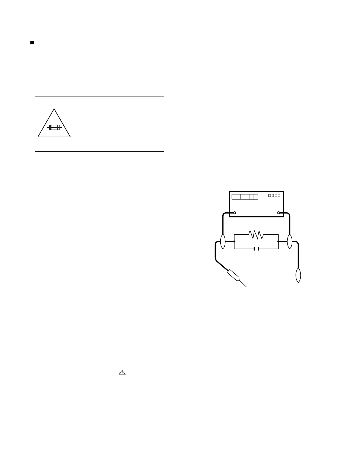
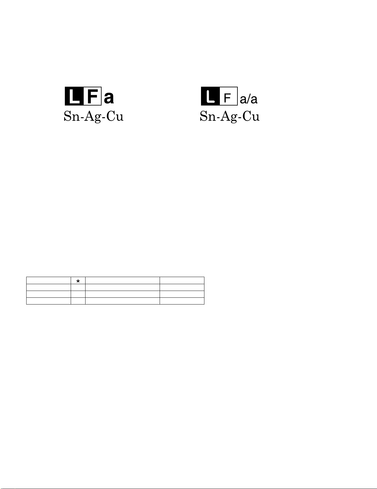
Employing lead-free solder
• "PWBs" of this model employs lead-free solder. The LF symbol indicates lead-free solder, and is attached on the PWBs and service manuals. The
alphabetical character following LF shows the type of lead-free solder.
Example:
Indicates lead-free solder of tin, silver and copper. Indicates lead-free solder of tin, silver and copper.
Using lead-free wire solder
• When fixing the PWB soldered with the lead-free solder, apply lead-free wire solder. Repairing with conventional lead wire solder may cause damage or accident due to cracks.
As the melting point of lead-free solder (Sn-Ag-Cu) is higher than the lead wire solder by 40 °C, we recommend you to use a dedicated soldering
bit, if you are not familiar with how to obtain lead-free wire solder or soldering bit, contact our service station or service branch in your area.
Soldering
• As the melting point of lead-free solder (Sn-Ag-Cu) is about 220 °C which is higher than the conventional lead solder by 40 °C, and as it has poor
solder wettability, you may be apt to keep the soldering bit in contact with the PWB for extended period of time. However, Since the land may be
peeled off or the maximum heat-resistance temperature of parts may be exceeded, remove the bit from the PWB as soon as you confirm the
steady soldering condition.
Lead-free solder contains more tin, and the end of the soldering bit may be easily corroded. Make sure to turn on and off the power of the bit as
required.
If a different type of solder stays on the tip of the soldering bit, it is alloyed with lead-free solder. Clean the bit after every use of it.
When the tip of the soldering bit is blackened during use, file it with steel wool or fine sandpaper.
• Be careful when replacing parts with polarity indication on the PWB silk.
Lead-free wire solder for servicing
Part No, Description Code
ZHNDAi123250E J φ0.3mm 250g(1roll) BL
ZHNDAi126500E J φ0.6mm 500g(1roll) BK
ZHNDAi12801KE J φ1.0mm 1kg(1roll) BM
iii
Page 6

LC-37D90U
LC-37D90U
CHAPTER 1. SPECIFICATIONS
[1] SPECIFICATIONS
Item Model: LC-37D90U
Service Manual
LCD panel
Number of dots
TV-standard
TV
Function
Receiving
Channel
Audio multiplex
Audio out
Terminals
Rear
VHF/UHF
CATV
Digital Terrestrial
Broadcast (8VSB)
Digital cable*
(64/256 QAM)
INPUT 1
INPUT 2
INPUT 3
INPUT 4
INPUT 5
Air ANTENNA
Cable ANTENNA
i.LINK
DIGITAL AUDIO OUTPUT
37" Advanced Super View & BLACK TFT LCD
6,220,800 dots (1920 1080 3 dots)
American TV Standard ATSC/NTSC System
VHF 2-13ch, UHF 14-69ch
1-135ch (non-scrambled channel only)
2-69ch
1-135ch (non-scrambled channel only)
BTSC System
10W 2
AV in, COMPONENT in
AV in, S-VIDEO in
HDMI in with HDCP
Audio in, HDMI in with HDCP
Audio in, DVI-I in with HDCP
75 Unbalance, F Type for VHF/UHF/Digital Air in 1
75 Unbalance, F Type for CATV/Digital Cable in 1
IEEE1394 2 with DTCP (Compatible with DTVLink)
Optical Digital audio output 1 (PCM/Dolby Digital)
OUTPUT
OSD language
Power Requirement
Power Consumption
w/o stand
Weight
with stand
Dimension
(W H D)
w/o stand
with stand
Accessories
Operating temperature
Audio out
English/French/Spanish
AC 120 V, 60 Hz
230 W
50.7 lbs./23.0 kg
62.9 lbs./28.5 kg
5
/8269/
36
5
/82845/
36
64
64
413/16inch
121/16inch
Remote control unit ( 1), AC cord ( 1), "AAA" size battery ( 2), Cable clamp ( 1),
Cable tie ( 1), Operation manual ( 1)
32°F to 104°F (0°C to 40°C)
* Emergency alert messages via Cable are unreceivable.
• As part of policy of continuous improvement, SHARP reserves the right to make design and specification changes for product
improvement without prior notice. The performance specification figures indicated are nominal values of production units.
There may be some deviations from these values in individual units.
1 – 1
Page 7
LC-37D90U
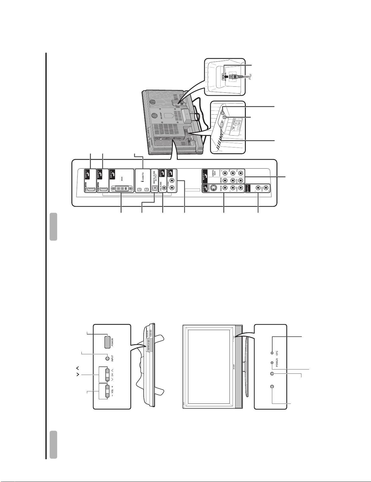
CHAPTER 2. OPERATION MANUAL
[1] OPERATION MANUAL
HDMI terminal(INPUT3)
HDMI terminal(INPUT4)
i.LINK terminals
LC-37D90U
Service Manual
AC INPUT terminal
AIR IN terminal
CABLE IN terminal
RS-232C terminal
Part names
INPUT button
POWER button
(INPUT5)
DVI terminal
OUTPUT
DIGITAL AUDIO
terminal
terminal
DVI AUDIO
INPUT1 terminals
terminals
(INPUT5)
(INPUT4)
AUDIO input
INPUT2
terminals
terminals
AUDIO OUTPUT
OPC indicator*
TV (Front) TV (Rear)
Part names
Channel buttons
(CH /)
+
-
VOL /)
Volume buttons (
2 – 1
Remote control sensor
OPC sensor*
POWER
indicator**
Page 8
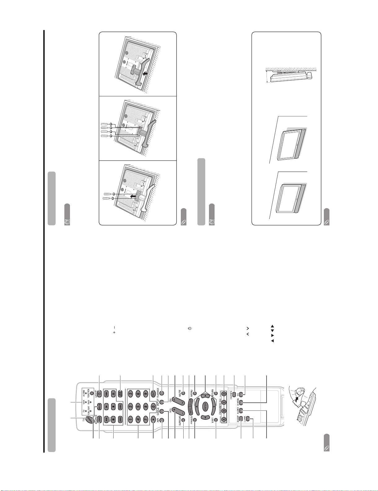
LC-37D90U
0° or 5°
Detach the stand from the TV.
(Hold the stand so it will not drop from
Unfasten the four screws used to
the edge of the base area.)
secure the stand in place.
About setting the TV angle
Angular mounting
3
CAUTION
Appendix
Before detaching (or attaching) stand, unplug the AC cord from the AC INPUT terminal.
standby mode.
1 TV POWER: Switches the TV power on or enters
2 DISPLAY: Displaysthe channel information.
• Do not remove the stand from the TV unless using an optional wall mount bracket to mount it.
3 SOURCE POWER: Turns the power of the external
Before attaching/detaching stand
equipment on and off.
damaged.
• Before performing work make sure to turn off the TV.
• Before performing work spread cushioning over the base area to lay the TV on. This will prevent it from being
the external equipment.
5 0–9:Sets the channel.
4 External equipment operational buttons: Operates
the stand in place.
SAT, VCR,DVD and AUDIO operation. Indicator lights up
17 FUNCTION: Switches the remote control for TV, CBL/
for the current mode.
23
NOTE
* To enter the code registration mode, you need to press
24
• To attach the stand, perform the above steps in reverse order.
time.
FUNCTION and DISPLAY at the same
18 LIGHT : When pressed all buttons on the remote
25
14 SLEEP: Sets the sleep timer.
15 i.LINK: Displays the i.LINK control panel.
20
Unfasten the screws used to secure
multi-channel audio broadcasts.
16 AUDIO: Selects the MTS/SAP or the audio mode during
21
12
normal screen.
6 • (DOT):
7AIR:Receives air signal.
18
8 CABLE: Receives cable signal.
9VOL/:Sets the volume.
10 SURROUND: Selects Surround settings.
19
11 INFO: Displays the program information screen.
13 EXIT: Turns off the menu screen.
12 FREEZE: Sets the still image. Press again to return to
control unit will light. The lighting will turn off if no
Setting the TV on the wall
operations are performed within about 5 seconds. This
button is used for performing operations in low-light
CAUTION
• Installing the TV requires special skill that should only be performed by quali-ed service personnel. Customers
situations.
19 VIEW MODE: Selects the screen size.
20 ENT: Jumps to a channel after selecting with the 0–9
28
27
should not attempt to do the work themselves. SHARP bears no responsibility for improper mounting or
mounting that results in accident or injury.
buttons.
21 FLASHBACK:Returns to the previous channel or
29
Using an optional bracket to mount the TV
external input mode.
• You can ask a quali-ed service professional about using an optional AN-37AG2 bracket to mount the TV to the
2, INPUT 3, INPUT 4, INPUT 5, i.LINK)
22 INPUT: Selects a TV input source. (TV, INPUT1, INPUT
30
wall.
• Carefully read the instructions that come with the bracket before beginning work.
23 CH / : Selects the channel.
31
Hangingonthewall
24 MUTE: Mutes the sound.
25 CH LIST: Displays the channel list screen.
AN-37AG2 wall mount bracket. (See the bracket instructions for details.)
26 MENU: Displays the menu screen.
27 ////ENTER: Selects a desired item on the
screen.
28 RETURN: Returns to the previous menu screen.
29 FAVORITE CH
A, B, C, D: Selects four preset favorite channels in four
different categories.
While watching, you can toggle the selected channels by
pressing A, B, C and D
30 FAVORITE:Registers favorite channels.
Vertical mounting
31 CC: Displays c aptio ns fr om a c losed- capt ion sourc e.
NOTE
STANDARD,MOVIE,GAME, USER,DYNAMIC(Fixed),
32 AV MODE: Selects an audio or video setting. (AVmode:
• Detach the cable clamp on the rear of the TV when using the optional mount bracket.
DYNAMIC.PC mode: STANDARD,MOVIE,GAME,
USER,DYNAMIC (Fixed),DYNAMIC, PC.)
Remote control unit Removing the stand
Part names
117
3
2
4
5
6
7228
9
102611
12
13
14
15
16 32
NOTE
• When using the remote control unit, point it at the TV.
2 – 2
Page 9
Possible Solution
PC
31.5 kHz
31.5 kHz
37.9 kHz
37.5 kHz
35.1 kHz
37.9 kHz
48.1 kHz
46.9kHz
48.4 kHz
56.5 kHz
60.0 kHz
64.0 kHz
47.7kHz
75.0 kHz
34.9 kHz
49.7 kHz
60.2 kHz
640 x 480
720 x 400
VGA
800 x 600SVGA
XGA 1024 x 768
WXGA
SXGA 1280 x 1024
1360 x 768
UXGA* 1600 x 1200
VGA 640 x 480
MAC13"
XGA 1024 x 768MAC19"
SVGA 832 x 624MAC16"
70 Hz
60 Hz
72 Hz
75Hz
56 Hz
60 Hz
72 Hz
75 Hz
60 Hz
70 Hz
75 Hz
60 Hz
60 Hz
60 Hz
67 Hz
75 Hz
75 Hz
OOOOOOOOOOOOO
Error code
setup.
• Check the antenna cable. Check that the antenna is correctly
E202
E203 • Check the broadcast time in the program guide.
Possible Solution
• Displayed when you have selected a device that is not compatible with the TV, or
that does not have DTLA copy protection technology installed.
Check the connection, and re-connect the cable if necessary.
• Displayed when a problem is experienced with a connection using i.LINK cable.
i.LINK connected device. To operate the selected device from the TV, you will first
• Displayed when the device you have selected is already being used by another
have to override control from the other device.
LC-37D90U
VESA StandardResolution
Vertical Frequency
Horizontal Frequency
Appendix
The example of an error
message displayed on a screen
The error message about reception of broadcast
Possible Solution
• Check if you pressed TV POWER on the remote control unit. If the
• No broadcast now.
• Failed to receive broadcast.
indicator on the TV does not light up, press POWER on the TV.
• Is the AC cord disconnected?
• Has the power been turned on?
The cautions about i.LINK
operation. In this case, operate the unit after fi-rst turning on the power of the TV or
unplugging the AC cord and replugging it in after 1 or 2 minutes.
• External influences such as lightning, static electricity, may cause improper
Caution sentence
• Record/Playback may fail on the
, ) aligned?
+
FUNCTION set correctly? Set it to the TV setting position.
•Isthe
• Are batteries inserted with polarity (
selected model.
• Are batteries worn out? (Replace with new batteries.)
• Are you using it under strong or fluorescent lighting?
connection was found. Refer to
• Wrong connection or no i.LINK
Is a fluorescent light illuminated near the remote control sensor?
•
Operation Manual on connection.
• The selected model is disabled to
• Is the image position correct?
• Are screen mode adjustments such as picture size made correctly?
record/play. Check that no other
model is used.
• Adjust the picture tone.
• Is the room too bright? The picture may look dark in a room that is too bright.
• Check the input signal setting.
PC compatibility chart
• Is the sleep timer set?
PC/MAC
• Check the power control settings.
• The unit's internal temperature has increased.
Remove any objects blocking vent or clean.
• Is connection to other components correct?
• Is correct input signal source selected after connection?
• Is the correct input selected?
• Is picture adjustment correct?
• Is "On" selected in "Audio Only"?
• Is a non-compatible signal being input?
• Is the volume too low?
• Is "Variable" selected in "Output Select"?
Apple and Macintosh are registered trademarks of Apple
Computer, Inc.
DDC is a registered trademark of Video Electronics
Standards Association.
Power Management is a registered trademark of Sun
Microsystems, Inc.
VGA and XGA are registered trademarks of International
*Digital input only.
++
Business Machines Co., Inc.
Problem
Troubleshooting Troubleshooting-Digital broadcasting
Appendix
• No power
• Unit cannot be operated.
operate.
• Remote control unit does not
screen.
• Picture is cut off/with sidebar
misalignment
• Strange color, light color, or color
• Power is suddenly turned off.
2 – 3
• No picture
• No sound
__
When the unit is used in a low temperature space (e.g. room, office), the picture may leave trails or appear slightly delayed.
This is not a malfunction, and the unit will recover when the temperature returns to normal.•Do not leave the unit in a hot or cold location. Also, do not leave the unit in a location exposed to direct sunlight or near a
heater, as this may cause the cabinet to deform and the Liquid Crystal panel to malfunction.
Cautions regarding use in high and low temperature environments
Storage temperature: 4°F to 140°F ( 20°C to 60°C)
•
Page 10

LC-37D90U
CONTROL CONTENTS
Effective only when the StandbyMode is set to "Mode1".
It input-switches by the toggle.(It is the same as an input change key)
It input-switches to TV. (Achannel remains as it is. (Last memory))
It input-switches to INPUT1~INPUT5.
It input-switches to i.LINK.
An input change is alsoincluded.
Although it can choose now,it is toggle operation in inside.
Only available when DVI ANALOGis being input.
Only available when DVI ANALOGis being input.
Although it can choose now,it is toggle operation in inside.
An input change is includedif it is not TV display.
In Air, 2–69ch is effective.
In Cable, 1–135ch is effective.
If it is not TVdisplay, it will input-switch to TV. (same function as CH )
If it is not TVdisplay, it will input-switch to TV. (same function as CH )
DIGITAL Cable (One-Part numbers, 5-digit,more than 10,000)
Toggle operation of a closedcaption.
AIR CABLE AIR(Toggle)ACSL 0_ __
_
+
DIGITAL Air (Two-Part numbers, 2-digitplus 2-digit)(0101-9999)
DIGITAL Cable (Two-Part numbers, 3-digitplus 3-digit)
DIGITAL Cable (Two-Part numbers, 3-digitplus 3-digit)
Front half of DIGITAL CABLECHANNEL NO. (Designate major channel)
Rear half of DIGITAL CABLECHANNEL NO. (Designate minor channel)
DIGITAL Cable (One-Part numbers, 5-digit,less than 10,000)
Appendix
Response code format
OK
Normal response
Return code (0DH)
ERR
Problem response (communication error or incorrect command)
Return code (0DH)
(Toggle)
Input terminal number (1–5)
Power Off
Power On1___
___
_
_______________
_______________
*
x
x
0
PARAMETER
ITGD
ITVD
IAVD
POWR
TV
INPUT1-5
CONTROL ITEM COMMAND
INPUT SELECTION A TOGGLE
POWER SETTING It shifts to standby.
Command table
• Commands not indicated here are not guaranteed to operate.
AUTO
VIDEO
COMPONENT
DIGITAL
ANALOG
(Toggle)
STANDARD
INP5
INPUT 5
MOVIE
12345
0
AVMD
AVMODE SELECTION
AUTO
___________
05612
INP1
LINKx___
i.LINK
INPUT 1
INPUT SELECTION B
GAME
USER
DYNAMIC (Fixed)
DYNAMIC
_
_
_
6
Volume(0–60)
AVmode. ( 10)
PC mode. (0–180)
PC
_____
_
_
*****
*
_
*****
*
___
*
*****
7
VOLM
HPOS
H-POSITIONH-POSITION
VOLUME
POSITION
AVmode. ( 20)
PC mode. (0–100)
Only PC mode. (0–180)
*
*
S
VPO
CLCK
V-POSITION
CLOCK
Only PC mode. (0–40)
(Toggle) [AV]
Side Bar [AV]
S.Stretch [AV]
Zoom [AV]
Stretch [AV]
_________
_________
_________
012345678
E
PHS
WIDE
PHASE
VIEWMODE
Normal [PC]
Zoom [PC]
(Toggle)
Stretch [PC]
Dot by Dot [AV] [PC]
On
Off
OFF
OFF TIMER – 30 MIN.
Full Screen [AV]9___
(Toggle)OnOff
___
___
___
1
MUT E0
The channel number of TV
(Toggle)
_
_
_
_
_
_
_
0
2
Ax___
U
ACS
ACH
(1–135)
OFF TIMER – 60 MIN.
OFF TIMER – 90 MIN.
OFF TIMER – 120 MIN.4___
_
_
_
_
_
*
___
_
_
*
___
_
_
*
112
2
3
0
M
OFT
H
DCC
DIRECT
(ANALOG)
CHANNEL
P** **
DA2
DIRECT
(0-999)
U** *_
DC2
(DIGITAL)
CHANNEL
The channel number of TV 1
The channel number of TV 1
(0-6383)
_
_
_
x
1****
DC1
CHUPCHDW
CH UP
_
_
_
x
CH DOWN
(Toggle)
AIR1___
CABLE2___
_
_
_
x
CLCP
(0-999)
(0-9999)
L***_
DC2
DC1 0 * * * *
X
NOTE
Surround
SLEEP TIMER
MUTE
AUDIO SELECTION
CHANNEL
Air/Cable SELECT
CC
• If an underbar (_) appears in the parameter column, enter a space.
• If an asterisk (*) appears, enter a value in the range indicated in brackets under CONTROL CONTENTS.
• As long as that from which the parameter ( ) in the table is a numerical value, it may write anything.
RS-232C port specifications
PC Control of the TV
Appendix
• When a program is set, the TV can be controlled from the PC using the RS-232C terminal. The input signal
(PC/AV) can be selected, the volume can be adjusted and various other adjustments and settings can be made,
enabling automatic programmed playing.
NOTE
connections.
• Attach an RS-232C cable cross-type (commercially available) to the supplied Din/D-Sub RS-232C for the
• This operation system should be used by a person who is accustomed to using computers.
Communication conditions
Set the RS-232C communication settings on the PC to match the TV's communication conditions.
The TV's communication settings are as follows:
9,600 bps
Baud rate:
8bits
Data length:
None
Parity bit:
1bit
Stop bit:
None
Flow control:
Communication procedure
Send the control commands from the PC via the RS-232C connector.
The TV operates according to the received command and sends a response message to the PC.
2 – 4
Do not send multiple commands at the same time. Wait until the PC receives the OK response before sending the
next command.
+
Eight ASCII codes CR
Command format
Command 4-digits: Command. The text of four characters.
Parameter 4-digits: Parameter 0 – 9, x, blank, ?
C1 C2 C3 C4 P1 P2 P3 P4
Command 4-digits Parameter 4-digits Return code
Input the parameter values, aligning left, and fill with blank(s) for the remainder. (Be sure that 4 values are input for
the parameter.)
When the input parameter is not within an adjustable range, "ERR" returns. (Refer to "Response code format".)
Parameter
0
Any numerical value can replace the "x" on the table.
30
0055
100
0009
_
?
When "?" is input for some commands, the present setting value responds.
????
Page 11

LC-37D90U
Setup
Picture
Picture
Menu items for TV/INPUT 1/INPUT 2 Menu items for HDMI/DVI
Basic adjustment settings
OPC
Backlight
OPC
Backlight
Contrast
Brightness
Color
Contrast
Brightness
Color
Tint
Sharpness
Advanced
Tint
Sharpness
Advanced
Color Temp.
Black
Monochrome
Color Temp.
Black
3D-Y/C
Audio
Film Mode
Range of OPC
Monochrome
Film Mode
Range of OPC
Audio
Treble
Bass
Treble
Balance
Surround
Bass
Balance
Power Control
Surround
Setup
Input Skip
Input Signal
Auto Sync.
Input Label
Fine Sync.
Position
Picture Flip
No Signal Off
No Operation Off
Power Control
EZ Setup
No Signal Off
No Operation Off
CH Setup
Standby Mode
Antenna Setup-DIGITAL
Input Skip
Input Label
Parental CTRL
Position
Language
Reset
Picture Flip
Standby Mode
Language
Reset
Option
Option
Audio Only
Digital Noise Reduction
Input Select
Audio Only
HDMI Setup
Output Select
Quick Shoot
Digital Noise Reduction
Input Select
Output Select
Quick Shoot
Digital Setup
Color System
Caption Setup
Program Title Display
Favorite CH
i.LINK Setup
Digital Setup
Audio Setup
i.LINK Setup
2 – 5
Page 12
LC-37D90U
LC-37D90U
CHAPTER 3. DIMENSIONS
[1] DIMENSIONS
3225/64(
27
26
36
822.6)
/64(671)
5
/8(
930)
Service Manual
Unit: inch/(mm)
4
(
104)
13
3
32
/
4
(
122)
16
/
729)
(
64
/
45
28
200)
(
8
/
7
7
664)
(
64
/
9
26
63)
(
64
/
31
2
100)
(
64
/
61
3
585)
(
32
/
1
23
77/8(
200)
463.8)
(
64
/
17
18
439)
(
32
/
9
17
12
1
/16(
306)
3 – 1
Page 13

LC-37D90U
CHAPTER 4. REMOVING OF MAJOR PARTS
Service Manual
[1] REMOVING OF MAJOR PARTS
1. Detach the SD Card Cover.
2. Remove the 2 lock screws and detach the Stand Cover.
3. Remove the 4 lock screws and detach the Stand.
4. Remove the SP Wire (L)(R). Remove the 4 lock screws and detach the Speaker Box.
5. Remove the 13 lock screws, 6 lock screws, 4 lock screws and detach the Rear Cabinet.
Front Cabinet
5
1
SD Card Cover
LC-37D90U
5
SP Wire (R)
4
5
Rear Cabinet
3
SP Wire (L)
2
Stand Cover
Stand
4
Speaker Box
4 – 1
Page 14
LC-37D90U
6. Remove the Stand Bottom Cover.
7. Disconnect the [FB] connector. Remove the 2 lock screws and detach the Fan Angle C Ass’y.
8. Remove the 4 lock screws and detach the SUS Angle (L)(R).
9. Remove the 5 lock screws and detach the Stand Fixing Angle.
10.Remove the 6 lock screws and detach the Main Shield.
10
Main Shield
SUS Angle (R)
8
7
SUS Angle (L)
Fan Angle C Ass'y
8
11.Disconnect all the connectors from all the PWBs.
Stand Fixing Angle
Stand Bottom Cover
9
4 – 2
Page 15

12.Remove the 3 lock screws and detach the Fan Angle L Ass’y.
13.Remove the 2 lock screws and detach the SP (L) PWB.
14.Remove the 3 lock screws and detach the SP Fixing Angle (L).
15.Remove the 2 lock screws and detach the SP (R) PWB.
16.Remove the 3 lock screws and detach the SP Fixing Angle (R).
17.Remove the 2 lock screws and detach the R/C, LED PWB.
18.Remove the 2 lock screws and detach the Top Control Cover.
19.Remove the 3 lock screws and detach the KEY PWB.
20.Remove the 4 lock screws and detach the Try Chassis.
18
Top Control Cover
KEY PWB
19
LC-37D90U
20
Try Chassis
12
Fan Angle L Ass'y
17
R/C, LED PWB
SP Fixing Angle (R)
16
SP (R) PWB
15
16
14
SP (L) PWB
SP Fixing Angle (L)
14
13
4 – 3
Page 16

LC-37D90U
21.Remove the 9 lock screws and detach the Jack Angle Long.
22.Remove the 6 lock screws and detach the POWER PWB.
23.Remove the 6 lock screws and detach the IF PWB.
24.Remove the 5 lock screws and detach the MAIN PWB Radiator and MAIN PWB.
24
MAIN PWB Radiator
MAIN PWB
21
21
22
POWER PWB
21
Jack Angle Long
23
IF PWB
25.Remove the 2 lock screws from the Panel Fixing Angle (C), the 2 lock screws from the Panel Fixing Angle (L)(R) and detach the LCD Panel Ass'y.
26.Remove the 3 lock screws and detach the Panel Fixing Angle (C).
27.Remove the 4 lock screws and detach the Panel Fixing Angle (L)(R).
Panel Fixing Angle (C)
27
Panel Fixing
Angle (R)
25
25
26
27
25
Panel Fixing
Angle (L)
4 – 4
Page 17

LC-37D90U
LC-37D90U
CHAPTER 5. ADJUSTMENT
Service Manual
[1] ADJUSTMENT PROCEDURE
The adjustment values are set to the optimum conditions at the factory before shipping. If a value should become improper or an adjustment is
required due to part replacement, make an adjustment according to the following procedure.
1. After replacement of any PWB unit and/or IC for repair, please note the following.
When replacing the following units, make sure to prepare the new units loaded with updated software.
MAIN Unit: DKEYDD743FM21
2. Upgrading of each microprocessor software
CAUTION: Never “POWER OFF” the unit when software upgrade is ongoing.
Otherwise the system may be damaged beyond recovery.
2.1. Software version upgrade
The model employs the following software.
•Main software
• Monitor microprocessor software
The main software and the monitor microprocessor software can be upgraded by using a general-purpose SD memory card.
The followings are the procedures for upgrading, explained separately for each of the main software, the monitor microprocessor software.
2.2. Main software version upgrade
2.2.1 Get ready before you start
• SD memory card of 32MB or higher capacity
• PC running on Windows 98/98SE/ME/2000/XP operating system
• SD memory card reader/writer with USB connectivity
• SD memory card formatting software
(Downloadable at http://panasonic.jp/support/audio/sd/download/sd_formatter_e.html)
2.2.2 Preparations
To upgrade the main software, it is necessary to get ready the SD card for version upgrade before you start. Follow the steps below and create the SD
card for version upgrade.
1. Insert the SD card into the SD card reader/writer. Start the SD card formatting software. Click [Format]. (When you have the drive options, select
the drive where the SD card is inserted before you proceed.)
5 – 1
Page 18

LC-37D90U
2. When the formatting is over, the following window appears. Click [OK].
3. Click [Exit] to finish the formatting.
NOTE: When you are done, take out the SD card once to make sure it is finished, and then insert it again.
4. Copy the binary image file OLYMAxxx.SDC (named temporarily) for version upgrade to the root directory (folder) of the SD card drive.
NOTE: In the SD card drive, do not store other folders or unrelated files, or more than one binary image files for version upgrade.
Now the SD card for version upgrade is ready.
2.2.3 Upgrading the software
1. Turn off the AC power (Unplug the AC power cord).
2. Insert the upgrading SD card (prepared as instructed above) into the service slot.
NOTE: Be careful not to insert the SD card in the wrong way. Otherwise the card may come into the set and fail to come out.
3. Turn on the AC power (Plug in the AC power cord).
4. A couple to dozen seconds after the set starts, the upgrade screen below shows up.
5 – 2
Page 19

LC-37D90U
5. If any of the procedures fails, the following upgrade failure screen shows up. For the failing procedure, the “NG” marking turns red.
NOTE: In such case, try to upgrade the software again. If it still fails, the hardware may be in trouble.
6. When all the procedures are complete, the following upgrade success screen shows up. The new software version can be confirmed on screen.
The version number appears when each item has been successfully upgraded. Finally the main version number appears on screen.
7. Turn off the AC power (Unplug the AC power cord). Take out the upgrading SD card.
8. Now the software has been upgraded.
NOTE: Then get the set started and call the process adjustment screen 1/27 to check the main software version.
CAUTION: 1) Do not take out and put in the SD memory card during formatting.
2) With the SD formatted, all the data stored on the medium will be deleted.
3) Do not start the SD formatting with the memory card’s WRITE PROTECT switch still on.
4) If the SD memory card format software does not recognize the SD memory card, take out and put in the SD memory card again, and
click the “UPDATE” button.
5) After checking the performance, use the set under its interface environment.
6) The SD formatting is impossible on drives that are not recognized “REMOVABLE”.
2.3. Upgrading the monitor microprocessor software
2.3.1 Kit
Have the above “Upgrading the main software” kit or equivalent at hand.
2.3.2 Preparations
As discussed in “Upgrading the main software” earlier, create the SD card for upgrading the monitor microprocessor software. For this SD card, use
the monitor microprocessor upgrading binary image file.
2.3.3 Upgrading procedure
To follow the monitor microprocessor software upgrading, the monitor screen upgrade progress indicator and the flashing power LED indicator can be
used.
1. Turn off the AC power (Unplug the AC power cord).
2. Insert the upgrading SD card (prepared as instructed above) into the service slot at the back of the set. Insert the SD card with its logo-printed face
upward (visible). Be careful not to insert the SD card in the wrong way. Otherwise the card may come into the set and fail to come out.
3. Turn on the AC power (Plug in the AC power cord).
CAUTION: Now the monitor microprocessor software starts getting upgraded. Be very careful not to turn off the power while the software is being
upgraded. Otherwise the software will fail to upgrade itself and the set will fail to get started.
5 – 3
Page 20

LC-37D90U
4. A couple to dozen seconds after the set starts, the upgrade screen below shows up. The upgrade progress is indicated on screen. The power LED
indicator goes out once and then starts flashing in blue. (It takes 2-3 minutes to get the monitor microprocessor software upgraded.)
5. If the procedure fails, the following upgrade failure screen shows up and the “NG” marking turns red. The power LED indicator fails to start flashing
in blue. Even if the usual screen reappears in several seconds, do the procedure from Step “1” again.
NOTE: In case of failure, try to upgrade the software again. If it still fails, the hardware may be in trouble.
6. When the procedure is complete, the following upgrade success screen shows up. The new software version can be confirmed on screen. The
upgrade success can also be confirmed when the power LED indicator and the OPC LED indicator start flashing alternately in blue and green,
respectively. Double-check the upgrading and turn off the AC power (Unplug the AC power cord). Take out the upgrading SD card. Now the software has been upgraded.
Finally get the set started and call the process adjustment screen 1/27 to check the monitor microprocessor software version.
5 – 4
Page 21

LC-37D90U
3. Entering and exiting the adjustment process mode
1) Before entering the adjustment process mode, the AV position RESET in the video adjustment menu.
2) While holding down the “VOL (–)” and "INPUT" keys at a time, plug in the AC cord of the main unit to turn on the power.
The letter “<K>” appears on the screen.
3) Next, hold down the “VOL (–)” and “CH ( )” keys at a time.
(The "VOL (–)" and "CH ( )" keys should be pressed and held until the display appears.)
Multiple lines of blue characters appearing on the display indicate that the unit is now in the adjustment process mode.
When you fail to enter the adjustment process mode (the display is the same as normal startup), retry the procedure.
4) To exit the adjustment process mode after the adjustment is done, unplug the AC cord from the outlet to make a forced shutdown. (When the
power was turned off with the remote controller, once unplug the AC cord and plug it again. In this case, wait 10 seconds or so before plugging.)
CAUTION: Use due care in handling the information described here lest your users should know how to enter the adjustment process mode. If the
4. Remote controller key operation and description of display in adjustment process mode
1) Key operation
Remote controller key Main unit key Function
CH ( / ) CH ( / )
VOL (+/–) VOL (+/–) Changing a selected item setting (+1/ –1)
Cursor (UP/DOWN) ————— Turing a page (PREVIOUS/NEXT)
Cursor (LEFT/RIGHT) ————— Changing a selected line setting (+10/ –10)
INPUT ————— Input switching (toggle switching)
ENTER ————— Executing a function
2) Description of display
settings are tampered in this mode, unrecoverable system damage may result.
Moving an item (line) by one (UP/DOWN)
(TUNER→INPUT1→INPUT2→INPUT3→INPUT4→INPUT5)
*Input mode is switched automatically when relevant adjustment is started so far as the necessary input signal is available.
(1) Current page/ (5) (6) LCD Panel size/Speaker type
Total pages
1/27 [INFO] INPUT5 AUTO USA 37_UNDER
MAIN Version 0.95 ( U 2006/02/02 1)
BOOT Version OLYM0.92
Monitor Version 0.88
EQ DATA CHECKSUM ROM (8) Parameters
TEMPAERATURE 7B
LAMP ERROR 0
NORMAL STANDBY CAUSE
ERROR STANDBY CAUSE 1) 0 2) 0 3) 0
(2) Current page title
(3) Current selected input
(4) Current color system
0
00H 00M 00H 00M 00H 00M
4) 0 5) 0
00H 00M 00H 00M
Destination
(7) Adjustment
process menu
header
5 – 5
Page 22

LC-37D90U
5. List of adjustment process mode menu
The character string in brackets [ ] will appear as a page title in the adjustment process menu header.
Page Line Item Description Remarks (adjustment detail, etc.)
1 [INFO]
1 MAIN Version Main software version
2BOOT Version
3 Monitor Version Monitor software version
4 EQ DATA CHECKSUM Audio data checksum
5 TEMPERATURE CPU temperature
6 LAMP ERROR Number of termination due to lamp error
7 NORMAL STANDBY CAUSE Refer to *1 under the list for details
8 ERROR STANDBY CAUSE Refer to *2 under the list for details
2 [INIT]
1 INDUSTRY INIT (Cause)
2 INDUSTRY INIT Initialization to factory settings .
3 HOTELMODE Hotel mode
4 Center Acutime Accumulated main operation time
5 RESET Reset
6 BacklightAcutime Accumulated monitor operation time
7 RESET Reset
8 LAMP ERROR RESET Reset LAMP ERROR
9 VIC XPOS X-coordinate setting for VIC READ
10 VIC YPOS Y-coordinate setting for VIC READ
11 VIC COLOR Collected color data setting for VIC READ
12 VIC SIGNAL TYPE Signal type setting for VIC READ
13 VIC READ Picture level acquisition function Level appears in green on the upper right.
3 [N358MAIN]
1 N358 ALL ADJ CVBS and TUNER signal level adjustment
2 N358 MAIN ADJ CVBS signal level adjustment
3 TUNER DAC ADJ TUNER signal level adjustment
4 N358 MAIN CONTRAST CVBS and TUNER contrast adjustment values
5 TUNER A DAC TUNER adjustment value
4 [TUNER TEST]
1 TUNER VCHIP TEST(69ch) Tuning test and VCHIP test (69 ch)
2 TUNER VCHIP TEST(7ch) Tuning test and VCHIP test (7 ch)
3 TUNER VCHIP TEST(10ch) Tuning test and VCHIP test (10 ch)
4 TUNER VCHIP TEST(15ch) Tuning test and VCHIP test (15 ch)
5 [COMP15KMAIN]
1 COMP15K MAIN ADJ Component 15K picture level adjustment (main)
2 COMP15K MAIN CONTRAST Contrast adjustment value
3 COMP15K MAIN Cb GAIN Cb GAIN adjustment value
4 COMP15K MAIN Cr GAIN Cr GAIN adjustment value
5 COMP15K Y OFFSET Y OFFSET adjustment value
6 COMP15K Cb GAIN Cb OFFSET adjustment value
7 COMP15K Cr GAIN Cr OFFSET adjustment value
6 [HDTV]
1 HDTV ADJ Component Hi-Vision picture level adjustment
2 CONTRAST Contrast adjustment value
3 Cb GAIN Cb GAIN adjustment value
4 Cr GAIN Cr GAIN adjustment value
5 HDTV Y OFFSET Y OFFSET adjustment value
6 HDTV Cb OFFSET Cb OFFSET adjustment value
7 HDTV Cr OFFSET Cr OFFSET adjustment value
7 [DVI ANALOG]
1 DVI ANALOG ADJ DVI ANALOG adjustment
2 R CUTOFF R CUTOFF adjustment value
3 G CUTOFF G CUTOFF adjustment value
4 B CUTOFF B CUTOFF adjustment value
5 R DRIVE R DRIVE adjustment value
6 G DRIVE G DRIVE adjustment value
7 B DRIVE B DRIVE adjustment value
5 – 6
Page 23

LC-37D90U
Page Line Item Description Remarks (adjustment detail, etc.)
8 [M GAMMA IN]
1 MONITOR GAMMA IN 1 Standard value 1(LEV60050) Adjustment gradation setting.
2 MONITOR GAMMA IN 2 Standard value 2(LEV60066)
3 MONITOR GAMMA IN 3 Standard value 3(LEV60116)
4 MONITOR GAMMA IN 4 Standard value 4(LEV60144)
5 MONITOR GAMMA IN 5 Standard value 5(LEV60200)
6 MONITOR GAMMA IN 6 Standard value 6(LEV60236)
7 GAMMA WRITE WB adjustment data writing
8 GAMMA RESET WB adjustment data reading
9 [M GAMMA R1]
1 MONITOR GAMMA R 1 WB adjustment Point 1, R adjustment value Parameter for six-point adjustment
2 MONITOR GAMMA G 1 WB adjustment Point 1, G adjustment value
3 MONITOR GAMMA B 1 WB adjustment Point 1, B adjustment value
4 MONITOR GAMMA R 2 WB adjustment Point 2, R adjustment value
5 MONITOR GAMMA G 2 WB adjustment Point 2, G adjustment value
6 MONITOR GAMMA B 2 WB adjustment Point 2, B adjustment value
7 MONITOR GAMMA R 3 WB adjustment Point 3, R adjustment value
8 MONITOR GAMMA G 3 WB adjustment Point 3, G adjustment value
9 MONITOR GAMMA B 3 WB adjustment Point 3, B adjustment value
10 GAMMA WRITE WB adjustment data writing
11 GAMMA RESET WB adjustment data reading
10 [M GAMMA R4]
1 MONITOR GAMMA R 4 WB adjustment Point 4, R adjustment value Parameter for six-point adjustment
2 MONITOR GAMMA G 4 WB adjustment Point 4, G adjustment value
3 MONITOR GAMMA B 4 WB adjustment Point 4, B adjustment value
4 MONITOR GAMMA R 5 WB adjustment Point 5, R adjustment value
5 MONITOR GAMMA G 5 WB adjustment Point 5, G adjustment value
6 MONITOR GAMMA B 5 WB adjustment Point 5, B adjustment value
7 MONITOR GAMMA R 6 WB adjustment Point 6, R adjustment value
8 MONITOR GAMMA G 6 WB adjustment Point 6, G adjustment value
9 MONITOR GAMMA B 6 WB adjustment Point 6, B adjustment value
10 GAMMA WRITE WB adjustment data writing
11 GAMMA RESET WB adjustment data reading
11 [SOUND 1]
1 AUDIO SELECT
2 INPUT_TRIM_SP
3 INPUT_TRIM_HP
4 CLIPPER_LEVEL
5ANGLE
6 MASTER_VOLUME
7 SCART_PRESCALE
8 FM_AM_PRESCALE
9 I2S1_PRESCALE
10 SCART1_VOLUME
11 SCART2_VOLUME
12 [SOUND 2]
1 AIN1_ADC_VOLUME
2 AIN2_ADC_VOLUME
3 AIN3_ADC_VOLUME
4 AIN4_ADC_VOLUME
5 AIN5_ADC_VOLUME
6 AIN6_ADC_VOLUME
5 – 7
Page 24

LC-37D90U
Page Line Item Description Remarks (adjustment detail, etc.)
13 [SOUND 3]
1 SUB_VOLUME_SURROUND
2SUB_VOLUME_FLAT
3 SUB_VOLUME_EQ
4 SUB_VOLUME_HP
5 SUB_VOLUME_HP_CENTERSP
6 SUB_VOLUME_CENTERSP_EQ
7 SUB_VOLUME_CENTERSP_FLAT
8 BBE_HF_ADJUST
9 BBE_LEVEL
10 BBE_MACH3_F0
11 BBE_MACH3_Q
12 BBE_MACH3_GAIN
14 [SOUND 4]
1EQ_MODE
2 PEQ1_F0
3 PEQ1_Q
4 PEQ1_GAIN
5 PEQ2_F0
6 PEQ2_Q
7 PEQ2_GAIN
8 PEQ3_F0
9 PEQ3_Q
10 PEQ3_GAIN
11 PEQ4_F0
12 PEQ4_Q
13 PEQ4_GAIN
15 [SOUND 5]
1 PEQ5_F0
2 PEQ5_Q
3 PEQ5_GAIN
4 EALA_GAIN
16 [M OPC1]
1 BRIGHTNESS DA0
2 BRIGHTNESS DA1
3 BRIGHTNESS DA2
4 BRIGHTNESS DA3
5 BRIGHTNESS DA4
6 BRIGHTNESS DA5
7 BRIGHTNESS DA6
8 BRIGHTNESS DA7
9 BRIGHTNESS DA8
10 BRIGHTNESS DA9
11 BRIGHTNESS DA10
12 BRIGHTNESS DA11
17 [M OPC2]
1 BRIGHTNESS DA12
2 BRIGHTNESS DA13
3 BRIGHTNESS DA14
4 BRIGHTNESS DA15
5 BRIGHTNESS DA16
6 BRIGHTNESS DA17
7 BRIGHTNESS DA18
8 BRIGHTNESS DA19
9 BRIGHTNESS DA20
10 BRIGHTNESS DA21
11 BRIGHTNESS DA22
5 – 8
Page 25

LC-37D90U
Page Line Item Description Remarks (adjustment detail, etc.)
18 [M OPC3]
1 BRIGHTNESS DA23
2 BRIGHTNESS DA24
3 BRIGHTNESS DA25
4 BRIGHTNESS DA26
5 BRIGHTNESS DA27
6 BRIGHTNESS DA28
7 BRIGHTNESS DA29
8 BRIGHTNESS DA30
9 BRIGHTNESS DA31
10 BRIGHTNESS DA32
19 [M ADL1]
1 OPC33 ADLEVEL 0
2 OPC33 ADLEVEL 1
3 OPC33 ADLEVEL 2
4 OPC33 ADLEVEL 3
5 OPC33 ADLEVEL 4
6 OPC33 ADLEVEL 5
7 OPC33 ADLEVEL 6
8 OPC33 ADLEVEL 7
9 OPC33 ADLEVEL 8
10 OPC33 ADLEVEL 9
11 OPC33 ADLEVEL 10
12 OPC33 ADLEVEL 11
20 [M ADL2]
1 OPC33 ADLEVEL 12
2 OPC33 ADLEVEL 13
3 OPC33 ADLEVEL 14
4 OPC33 ADLEVEL 15
5 OPC33 ADLEVEL 16
6 OPC33 ADLEVEL 17
7 OPC33 ADLEVEL 18
8 OPC33 ADLEVEL 19
9 OPC33 ADLEVEL 20
10 OPC33 ADLEVEL 21
11 OPC33 ADLEVEL 22
21 [M ADL3]
1 OPC33 ADLEVEL 23
2 OPC33 ADLEVEL 24
3 OPC33 ADLEVEL 25
4 OPC33 ADLEVEL 26
5 OPC33 ADLEVEL 27
6 OPC33 ADLEVEL 28
7 OPC33 ADLEVEL 29
8 OPC33 ADLEVEL 30
9 OPC33 ADLEVEL 31
22 [M V6THE]
1V6 OS THERMO 1
2V6 OS THERMO 2
3V6 OS THERMO 3
4V6 OS THERMO 4
5V6 OS THERMO 5
6V6 OS THERMO 6
7V6 OS THERMO 7
23 [M V5THE]
1V5 OS THERMO 1
2V5 OS THERMO 2
3V5 OS THERMO 3
4V5 OS THERMO 4
5V5 OS THERMO 5
6V5 OS THERMO 6
7V5 OS THERMO 7
5 – 9
Page 26

LC-37D90U
Page Line Item Description Remarks (adjustment detail, etc.)
24 [M EEP SET]
1 MONITOR TIME OUT
2 MONITOR MAX TEMP
3 MONITOR STANDBY CAUSE
25 [M TESTPTRN]
1 LCD TEST PATTERN
26 [MEMORY CLR]
1 KEY LOCK(1217)
2 KOUTEI AREA ALL CLEAR
3 A MODE AREA CLEAR
4 BACKUP AREA CLEAR
5 B MODE AREA CLEAR
6EXECUTION
27 [ETC]
1 EEP SAVE Writing setting values to EEPROM.
2 EEP RECOVER Reading setting values from EEPROM.
3 STANDBY CAUSE RESET Reset stand by cause.
*1 Details of P1.7(NORMAL STANDBY CAUSE)
6 No operation off in the cause of “no operation off”
7 No signal off in the cause of “no signal off”
8 PC power management mode 1 in the cause of “Standby mode MODE1”
9 PC power management mode 2 in the cause of “Standby mode MODE2”
A Off timer in the cause of “SLEEP timer”
C Command from RS232C in the cause of command by RS-232C
*2 Details of P1.8(ERROR STANDBY CAUSE)
5 Prolonged unspecified-signal input in PC mode in the cause of continuous “out of range”, PC input mode
13 Temperature error in the cause of abnormal temperature
16 Monitor trouble detected in the cause of abnormal monitor mode
17 Fan lock in the cause of fan lock
6. Special features
* STANDBY CAUSE (Page 1/27)
Display of a cause (code) of the last standby
The cause of the last standby is recorded in EEPROM whenever possible.
Checking this code will be useful in finding a problem when you repair the troubled set.
* EEP SAVE (Page 27/27)
Storage of EEP adjustment value
* EEP RECOVER (Page 27/27)
Retrieval of EEP adjustment value from storage area
7. Video signal adjustment procedure
*Adjustment process mode menu is listed in section 5.
7.1. Signal check
Signal generator level adjustment check (Adjustment to the specified level)
• Composite signal : 0.714Vp-p ± 0.02Vp-p (Pedestal to white level)
• 15K component signal : Y level : 0.714Vp-p ± 0.02Vp-p (Pedestal to white level)
PB, PR level : 0.7Vp-p ± 0.02Vp-p
• 33K component signal : Y level : 0.7Vp-p ± 0.02Vp-p (Pedestal to white level)
PB, PR level : 0.7Vp-p ± 0.02Vp-p
• DVI-I (analog RGB) signal : RGB level : 0.7Vp-p ± 0.02Vp-p (Pedestal to white level)
7.2. Entering the adjustment process mode
Enter the adjustment process mode according to the steps described in section 3.
5 – 10
Page 27
7.3. N358 composite signal adjustment (Tuner)
Adjustment item Adjustment conditions Adjustment procedure
1 Adjustment N358 signal Feed the PAL split field color bar signal (75% color saturation) to VIDEO
1 input. Feed the RF signal (by use of US-10ch) to TUNER-A.
[Video input signal] [US-10CH]
100% white 100% white
2 Auto adjustment
performance
Page 3/27 Bring the cursor on [•N358 ALL ADJ] and press [ENTER].
[•N358 ALL ADJ FINISH] appears when finished.
7.4. Component 15K signal adjustment
Adjustment item Adjustment conditions Adjustment procedure
1 Adjustment 480i signal Feed the 100% color bar signal to INPUT 1 component input.
LC-37D90U
100% white
2 Auto adjustment
performance
Page 5/27 Bring the cursor on [•COMP 15K ALL ADJ] and press [ENTER].
[•COMP 15K ALL ADJ FINISH] appears when finished.
7.5. Component 33K signal adjustment
Adjustment item Adjustment conditions Adjustment procedure
1 Adjustment 1080i signal Feed the 100% color bar signal to INPUT 1 component input.
100% white
2 Auto adjustment
performance
Page 6/27 Bring the cursor on [•HDTV ADJ] and press [ENTER].
[•HDTV ADJ FINISH] appears when finished.
7.6. DVI-I (analog) signal adjustment
Adjustment item Adjustment conditions Adjustment procedure
1 Adjustment DVI-I (analog)
XGA (1024 x 768)
60Hz
H,V SYNC
Feed the 100% white 1/2 window pattern signal to DVI-I (analog) input.
1/4
1/2
1/4
5 – 11
1/4
1/2
100% White
0% Black
1/4
Page 28

LC-37D90U
Adjustment item Adjustment conditions Adjustment procedure
2 Auto adjustment
performance
8. Adjustment of white balance
8.1. White balance adjustment
Adjustment item Adjustment conditions Adjustment procedure
1 Adjustment 1) Apply the following settings to the set.
2 Auto adjustment
performance
Page 7/27 Bring the cursor on [•DVI ANALOG] and press [ENTER].
[•DVI ANALOG ADJ FINISH] appears when finished.
AV MODE: [DYNAMIC]
Aging Time: 60 Min.
Backlight: +16
2) Connect a white balance jig and the set.
Optical measuring machine: [Minolta CA-210]
PC
RS-232C communication cable
3) Use an RS-232C command to display the screen for multipoint adjustment.
•Multipoint adjustment mode (MSET0001)
•Adjustment value initialization (MSET0004)
•Standard value 6 (LEV60232)
•Standard value 5 (LEV50200)
•Standard value 4 (LEV40164)
•Standard value 3 (LEV30132)
•Standard value 2 (LEV20088)
•Standard value 1 (LEV10048)
•Write setting (MSET0003)
[Adjustment]
1) Enter the monitor adjustment process mode.
2) Set the specified gradation for standard value 6. Set the strongest
color as the fixed color and adjust RGB by reducing to the standard
value.
3) Set the specified gradation for standard value 5. Set the correction
value of G [(default of standard value 5) x (G of standard value 6) /
(default of standard value 6)] and adjust RB to the standard value.
4) Set the specified gradation for standard value 4. Set the correction
value of G [(default of standard value 4) x (G of standard value 6) /
(default of standard value 6)] and adjust RB to the standard value.
5) Set the specified gradation for standard value 3. Set the correction
value of G [(default of standard value 3) x (G of standard value 6) /
(default of standard value 6)] and adjust RB to the standard value.
6) Set the specified gradation for standard value 2. Set the correction
value of G [(default of standard value 2) x (G of standard value 6) /
(default of standard value 6)] and adjust RB to the standard value.
7) Set the specified gradation for standard value 1. Set the correction
value of G [(default of standard value 1) x (G of standard value 6) /
(default of standard value 6)] and adjust RB to the standard value.
8) Write the adjustment values with MSET0003 command and turn off
AC power.
[Adjustment values]
Optical measuring machine: [Minolta CA-210] (Focus on the center of the screen.)
Level Standard value Adjustment value Tolerance
Standard value 6 232 x = 0.272 ±0.001 ±0.0020
y = 0.272 ±0.001 ±0.0020
Standard value 5 200 x = 0.272 ±0.001 ±0.0020
y = 0.272 ±0.001 ±0.0020
Standard value 4 164 x = 0.272 ±0.001 ±0.0020
y = 0.272 ±0.001 ±0.0020
Standard value 3 132 x = 0.272 ±0.001 ±0.0020
y = 0.272 ±0.001 ±0.0020
Standard value 2 88 x = 0.272 ±0.002 ±0.004
y = 0.272 ±0.002 ±0.004
Standard value 1 48 x = 0.272 ±0.002 ±0.004
y = 0.272 ±0.002 ±0.004
5 – 12
Page 29

LC-37D90U
Level Standard value Adjustment value Tolerance
Note Set the following before adjustment.
AV MODE: [DYNAMIC]
Monochrome: ON
Aging Time: 60 Min.
8.2. Adjusting procedure by use of [RS-232C]
1. Get ready the PC with COM port (RS-232C) running on Windows 95/98/ME/2000/XP operating system, as well as the RS-232C cross cable.
2. Start the unit with the RS-232C cable connected.
3. Start the terminal software. (The freeware readily available on the Internet will do.)
4. Make the following settings.
Baud rate 9,600 bps
Data LENGTH 8 bit
Parity bit None
Stop bit 1 bit
Flow control None
5. If the settings are correct, the terminal software indicates “ERR” against pressing of the “ENTER” key.
6. After the settings are done correctly, it is possible to make an adjustment by typing in the command shown in the table below and pressing the
“ENTER” key on the keyboard.
7. Command entry is successful if the terminal software indicates “OK” when the “ENTER” is pressed. If “ERR” is shown, retry to enter the command.
8. Send the process mode switching command to switch from the RS232C operation mode to the process mode.
KRSW0001: “ERR” is returned.
KKT10037: When “OK” is returned, the process mode becomes active. When “ERR”, start over from KRSW0001.
9. Send each adjustment command.
5 – 13
Page 30
LC-37D90U
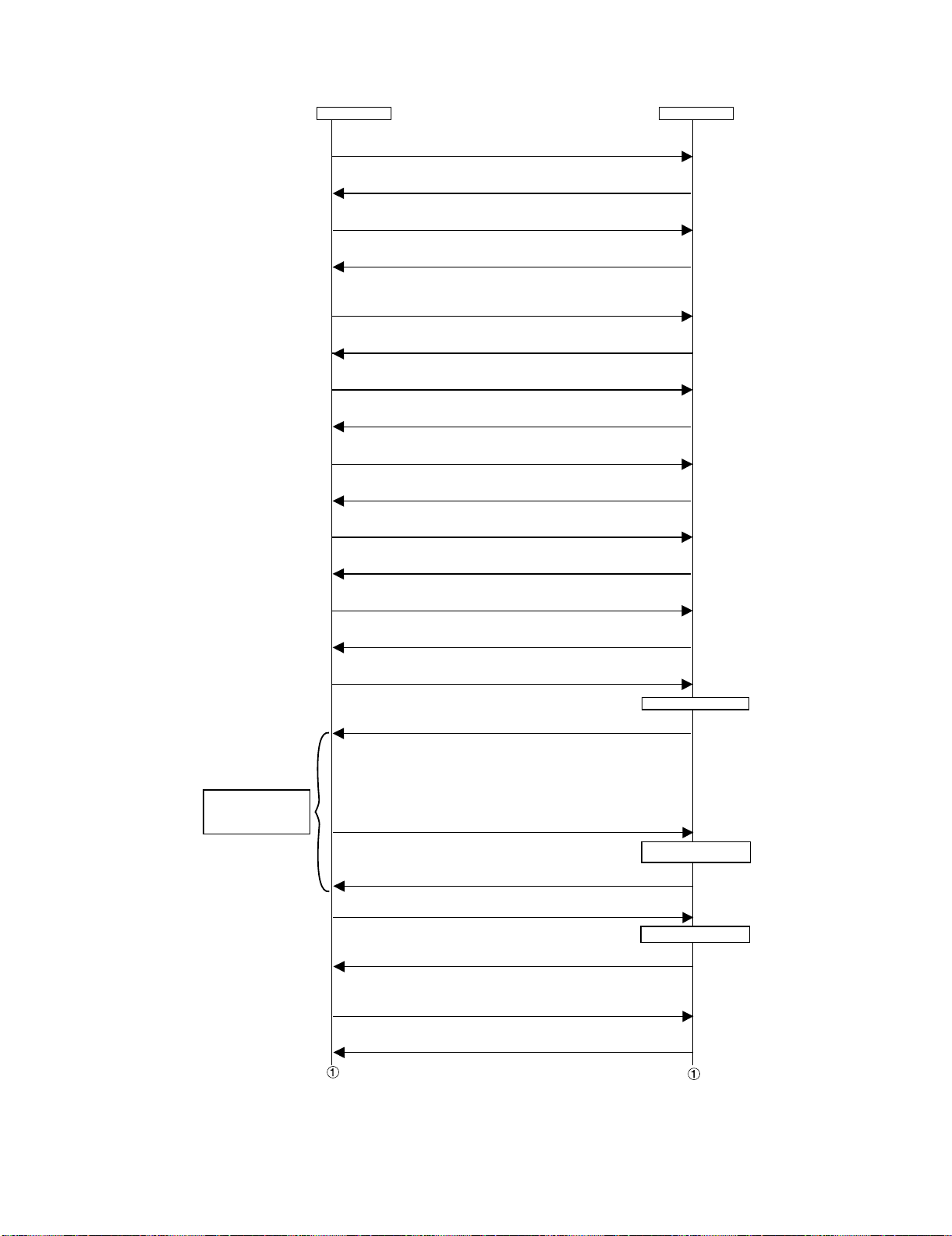
8.3. White balance adjustment sequence
Adjustment is available in any input or position. There is no specific order to adjust high and low, either.
Repeat until values are
properly
adjusted.
PC
Activate process command (STEP1).
KRSW0001
Command is accepted.
ERR
Activate process command (STEP2).
KKT10037
Process command is
activated.
OK
Remote control
disable command
KYOF0000
Setting is complete.
OK
Inhibit command for the OSD display
OSDS0001
Setting is complete.
OK
Set the light level to +12 using dimmer control command.
SBSL0016
Setting is complete.
OK
Set the multipoint adjustment mode.
MSET0001
The mode is set.
OK
Initialize adjustment values.
MSET0004
Initialization is done.
OK
Adjustment gradation setting (Standard value 6 = 236 gradation)
LEV60232
Adjustment value is set.
Adjust RGB to the target xy values.
MG6GXXXX
MG6BXXXX
MG6RXXXX
* XXXX indicates adjustment values between 0000 - 1023 (4 digit decimal
number with zero fill).
*
In order to adjust by reducing the value, set the strongest color as the fixed color.
* Default adjustment value of RGB is the parameter value of LEV6 command
multiplied by 4.
Adjustment gradation setting (Standard value 5 = 200 gradation)
LEV50200
Correct G value.
MG5GXXXX
When G is changed at adjustment gradation setting (standard value 6 = 236 gradation), calculate the ratio of the
change and set the following value to XXXX: (the value set with LEV5) x 4 x (the ratio).
OK
Adjustment values are set.
OK
Adjustment value is set.
OK
Adjustment value is set.
OK
Pattern display
Reflecting adjustment
values to images
Pattern display
Set
5 – 14
Page 31

Repeat until values are
properly adjusted.
Start of measurement
Adjust RB to the target xy values.
MG5RXXXX
MG5BXXXX
* XXXX indicates adjustment values between 0000 - 1023 (4 digit decimal number with zero fill).
* G is fixed.
* Default adjustment value of RGB is the parameter value of LEV5 command multiplied by 4.
Adjustment values are set.
Adjustment gradation setting (Standard value 4 = 144 gradation)
LEV40164
OK
Reflecting adjustment values to
images
LC-37D90U
Repeat until values are
properly adjusted.
Repeat until values are
properly adjusted.
Adjustment value is set.
Correct G value.
MG4GXXXX
When G is changed at adjustment gradation setting (standard value 6 = 236 gradation), calculate
the ratio of the change and set the following value to XXXX: (the value set with LEV4) x 4 x (the ratio).
Start of measurement
Adjust RB to the target xy values.
MG4RXXXX
MG4BXXXX
* XXXX indicates adjustment values between 0000 - 1023 (4 digit decimal number with zero fill).
* G is fixed.
* Default adjustment value of RGB is the parameter value of LEV4 command multiplied by 4.
Adjustment gradation setting (Standard value 3 = 116 gradation)
LEV30132
Correct G value.
MG3GXXXX
When G is changed at adjustment gradation setting (standard value 6 = 236 gradation), calculate
the ratio of the change and set the following value to XXXX: (the value set with LEV3) x 4 x (the ratio).
Start of measurement
Adjust RB to the target xy values.
MG3RXXXX
MG3BXXXX
* XXXX indicates adjustment values between 0000 - 1023 (4 digit decimal number with zero fill).
* G is fixed.
* Default adjustment value of RGB is the parameter value of LEV3 command multiplied by 4.
OK
Adjustment value is set.
OK
Reflecting adjustment values to
Adjustment values are set.
OK
Adjustment value is set.
OK
Adjustment value is set.
OK
Pattern display
images
Pattern display
Reflecting adjustment values to
Adjustment values are set.
OK
Adjustment gradation setting (Standard value 2 = 66 gradation)
LEV20088
Adjustment value is set.
Correct G value
MG2GXXXX
When G is changed at adjustment gradation setting (standard value 6 = 236 gradation), calculate
the ratio of the change and set the following value to XXXX: (the value set with LEV2) x 4 x (the ratio).
OK
Adjustment value is set.
OK
Pattern display
5 – 15
images
Page 32

LC-37D90U
Repeat until values are
properly adjusted.
Repeat until values are
properly adjusted.
Start of measurement
Adjust RB to the target xy values.
MG2RXXXX
MG2BXXXX
* XXXX indicates adjustment values between 0000 - 1023 (4 digit decimal number with zero fill).
* G is fixed.
* Default adjustment value of RGB is the parameter value of LEV2 command multiplied by 4.
Reflecting adjustment values to
Adjustment values are set.
OK
Adjustment gradation setting (Standard value 1 = 50 gradation)
LEV10048
Adjustment value is set.
OK
Correct G value.
MG1GXXXX
When G is changed at adjustment gradation setting (standard value 6 = 236 gradation), calculate
the ratio of the change and set the following value to XXXX: (the value set with LEV1) x 4 x (the ratio).
Adjustment value is set.
OK
Start of measurement
Adjust RB to the target xy values.
MG1RXXXX
MG1BXXXX
* XXXX indicates adjustment values between 0000 - 1023 (4 digit decimal number with zero fill).
* G is fixed.
* Default adjustment value of RGB is the parameter value of LEV1 command multiplied by 4.
Reflecting adjustment values to
Adjustment values are set.
OK
Save adjustment values.
MSET0003
Adjustment values are saved.
OK
Completion of adjustment
Turn off AC power
images
Pattern display
images
9. Initialization to factory settings
CAUTION: When initialization is performed, all user setting data including the channel settings are initialized. Be cautious when making this adjust-
ment.
(The adjustments done in the adjustment process mode are not initialized.)
Adjustment item Adjustment conditions Adjustment procedure
1 Initialization It turns off with AC power
supply.
After the adjustment, cancel the adjustment process mode.
To exit the adjustment process mode, unplug the AC power cable from the outlet to make a
forced shutdown. (When the power was turned off with the remote controller, once unplug the
power cable and plug it again. In this case, wait 10 seconds or so before plugging.)
Enter the adjustment process mode.
Bring the cursor on to [INDUSTRY INIT] in page 2/27.
Set to [ON] using [VOL] key, and press [ENTER] to execute the initialization.
When the version number screen shows up on the green background and “SUCCESS”
gets displayed at the top on screen, it means the procedure has been successfully carried out.
(If an error occurs, “ERROR” is displayed on the red background.)
•Turn off the AC power.
*Never shut off the power during the initialization process.
The following settings are initialized in this adjustment.
1) User setting
2) Channel data (e.g. broadcast frequencies)
3) Password data
4) Operation time
5) Auto installation flag
6) V-CHIP block setting
5 – 16
Page 33

LC-37D90U
[2] MAJOR IC INFORMATIONS
1. MAJOR IC INFORMATIONS
1.1. IC501 (MM1630CQ)
This I2C bus-controlled video switch is designed to switch between one-system color difference (component) signal, one-system S video signal and
two-system composite signal.
The analog video signal from the INPUT-1 or INPUT-2 input terminal is fed into this IC for selection. The video output signal from this IC flows through
a low-pass filter into the video signal processing circuit IC3301 (IXB723WJ).
1.2. IC2701 (VHiTA2024++-1Y)
The Class-T type digital audio power amplifier TA2024 gives maximum continuous output of 10 W/ch.
1.3. IC1401 (VHiAN5832SA-1Y)
The AN5832SA is an I2C bus-controlled, US-standard analog TV sound multiplexing demodulator IC. It has the following functions built in: SIF
demodulation, STEREO demodulation, SAP demodulation, dbx noise reduction, and audio AGC.
1.4. IC1403 (VHiAK4683EQ-1Q)
This IC provides for 2-channel A/D and 4-channel D/A (192-kHz sampling).
The built-in digital audio interfaces DIR (Digital Interface Receiver) and DIT (Digital Interface Transmitter) (192 kHz compatible, 6 inputs/1 output) are
compatible with the AES3, IEC60958, S/PDIF, and EIAJ CP1201 standards. Both the DIR and DIT can handle 192-kHz sampling and 24-bit data. The
DIR is also equipped with 6-channel input selector that detects not just PCM data but also Dolby Digital and other non-PCM data.
1.5. IC1406 (VHiNJU26111-1Q)
The 24-bit, DSP core, digital audio processor has the Circle Surround II 5.1, TruSurround XT, Tru Bass, Focus, and Mono-To-Stereo functions. The
Circle Surround II 5.1 feature converts matrix-encoded stereo signals to theater-like 5.1-channel sounds. Un-matrix-encoded signals are also converted to effects-rich 5.1-channel output. The TruSurround XT feature creates three-dimensional sounds, richer than stereo signals.
1.6. IC1507 (VHiTMDS341+-1Y)
The TMDS341 single-chip IC is provided with multiple switching function, in which up to 3 DVI/HDMI ports can be selected for a single display input
terminal.
This 3-port device is also equipped with signal conditioning function and switching function. Each of the ports supports 4-channel TMDS signal, one
hot plug detection, and I2C interface. Each of the 4 TMDS channels, in turn, provides maximum 1.65-Gbps signal transmission rate, fixed 8-dB input
equalization, and enable/disable 3-dB output deemphasis function.
On this IC, the INPUT-3/4 HDMI port and the INPUT-5 DVI port are switched.
1.7. IC1508 (VHiSii9011L-1Q)
The TMDS receiver IC decodes differential serial-transmitted signal to parallel signal. Compatible with the HDCP system, encrypted signals can also
be received.
This IC responds to the INPUT-3/4 HDMI (High-Definition Multimedia Interface) and the INPUT-5 DVI (Digital Visual Interface) selected by IC507.
1.8. IC2002 (RH-iXB345WJZZQ)
The monitor microprocessor is intended to communicate with the main microprocessor and to operate the system. It also controls power of the entire
system.
1.9. IC3301 (RH-iXB723WJQZQ)
This video processor consists of an LSI system-on-chip device. For high-precision data processing, it is equipped with a high-precision 166-MHz, 10bit A/D converter.
For processing analog video signals, this IC supports the NTSC-compatible high-performance multi-format 2D/3D digital Y/C separation video
decoder as well as the video format conversion engine. It provides for 10-bit video signal processing.
1.10. IC3501/3502 (RH-iXB375WJZZQ)
These ICs are 128-Mbit GDDR SDRAM (Graphic Double Data Rate Synchronous DRAM), providing a memory for image processing and buffering
OSD data.
5 – 17
Page 34

LC-37D90U
1.11. IC8101 (RH-iXB281WJZZQ)
This LSI with MPEG-2 system decoder performs back-end processing for digital broadcasting. It is equipped with a CPU (processor core: AM33-3),
descrambler (DES), transport stream de-multiplexer, video decoder (MPEG-2 MP@HL compatible), graphic processor, audio decoder (AC3 compatible), and an NTSC video encoder.
After receiving transport stream from the tuner, the LSI decrypts pay-TV broadcasts with the descrambler. Then using the de-multiplexer, it separates
and decodes the compressed audio and video data to send the signals. In the visual system, the graphic processor makes it possible to overlap subtitles and perform scaling. Digital video signals (Y, Pb and Pr, or 480I/P, 720P and 1081I) and down-converted NTSC signals (Y/C and composite, or
480I) can be sent simultaneously. As for the audio system, decoded AC3 audio can be overlapped with sound effects.
The LSI also contains various interfaces (I2C x 2, UART x 3, an SD Memory Card interface, a Cable CARD interface, etc.) and a GPIO. Using these
interfaces, the CPU controls peripheral circuits of the tuner, SD Memory Cards, Cable CARDs, etc. One of the UARTs is used by the CPU to establish
communications with the monitor microcomputer in the unit, where remote control information or other data is exchanged. Another UART is used for
RS-232C serial communications to connect the unit to a PC.
1.12. IC8301/8302/8303/8304 (RH-iXB024WJZZQ)
These are 256-Mb (4 Mb x 16 I/O x 4 banks) F-die DDR SDRAMs.
1.13. IC8451 (VHiS29GL64A-1Q)
The 64-Mbit page mode flash memory device stores the main CPU program.
1.14. IC8503 (RH-iXB323WJZZQ)
The IEEE 1394a Link-Layer Controllers with Integrated 2-Port PHY provide DTLA encryption support for MPEG2-DVBS, DSS and Audio Data.
1.15. IC8601 (RH-iXB684WJQZQ)
The RH-IXB684WJQZQ comprises a family of advanced QAM and VSB demodulator for the Digital Cable Ready and ATSC environments.
This IC is configurable to operate in either the ITU-J.83B/SCTE DVS-031 compliant 64 QAM or 256 QAM modes used by digital cable systems, or the
ATSC compliant 8VSB mode used in digital terrestrial broadcasting.
For digitally modulated input signals (QAM or 8VSB), the RH-IXB684WJQZQ outputs a parallel or serial MPEG compliant transport stream.
1.16. IC8702 (VHiTC6384AF1EQ)
This is a Standard Memory Interface to SD Memory Controller.
1.17. IC9101 (RH-iXB732WJQZQ)
The high-performance CPLD (Complex Programmable Logic Device) is controlled by the main CPU to send control signals to various mounted
devices.
5 – 18
Page 35

2. MAJOR IC INFORMATIONS (BLOCK DIAGRAM AND PIN FUNCTION)
2.1. VHiMM1630CQ-1Q (ASSY: IC501)
Video Switch with I2C-bus
• Block Diagram [VHiMM1630CQ-1Q (ASSY: IC501)]
LC-37D90U
• Pin Function [VHiMM1630CQ-1Q (ASSY: IC501)]
Pin No. Pin Name I/O Pin Function
1 C3 I Chroma signal input.
7C4 I
13 C5 I
69 C1 I
75 C2 I
2 S-3 I SW of S-terminal.
6S-4 I
12 S-5 I
70 S-1 I
76 S-2 I
3 V4 I Composite signal input.
9V5 I
15 V6 I
17 V7 I
19 V8 I
63 VIN I
65 V1 I
71 V2 I
77 V3 I
5 – 19
Page 36

LC-37D90U
Pin No. Pin Name I/O Pin Function
4 S2-4 I Detect of S-terminal.
10 S2-5 I
68 S2-1 I
74 S2-2 I
80 S2-3 I
5 Y4 I Luminance signal input.
11 Y 5 I
67 Y1 I
73 Y2 I
79 Y3 I
8,47,53,57 Vcc --- Power supply.
14 ADR I Slave address select terminal.
16 BIAS I Bias.
18,44,62 GND --- GND.
20 L11 I Detect of D-terminal scanning line.
26 L12 I
32 L13 I
21 CY1 I Color difference siganl input.
27 CY2 I
33 CY3 I
39 CY4 I
22 L21 I Detect of D-terminal I/P.
28 L22 I
34 L23 I
23 PB1 I Color difference siganl input.
29 PB2 I
35 PB3 I
41 PB4 I
24 L31 I Detect of D-terminal aspect ratio.
30 L32 I
36 L33 I
25 PR1 I Color difference siganl input.
31 PR2 I
37 PR3 I
43 PR4 I
38 SW1 I Switch for a D-terminal connection check.
40 SW2 I
42 SW3 I
45 SDA I/O DATA in-output of I2C bus.
46 SCL I CLK input of I2C bus.
48 VOUT4 O Composite signal output for teletexts.
61 VOUT O Composite signal output for GRS.
49 DCOUT O S-DCOUT.
50 COUT3 O Monitor output (75Ω can drive).
51 VOUT3 O
52 YOUT3 O
54 PROUT2 O Color difference siganl output.
58 PROUT1 O
55 PBOUT2/COUT2 O Color difference signal/Chroma signal output.
59 PBOUT1/COUT1 O
56 CYOUT2/YOUT2/VOUT2 O Color difference signal/Luminance signal/Composite signal output.
60 CYOUT1/YOUT1/VOUT1 O
64 O1 O General-purpose output.
66 O2 O
72 O3 O
78 O4 O
5 – 20
Page 37

2.2. VHiTA2024++-1Y (ASSY: IC2303)
STEREO DIGITAL AUDIO AMPLIFIER
• Block Diagram [VHiTA2024++-1Y (ASSY: IC2303)]
LC-37D90U
• Pin Function [VHiTA2024++-1Y (ASSY: IC2303)]
Pin No. Pin Name I/O Pin Function
2,3 DCAP2,
4,9 V5D, V5A --- Digital 5VDC, Analog 5VDC.
5,8,17 AGND1,
6 REF --- Internal reference voltage; approximately 1.0 VDC.
7 OVERLOADB A logic low output indicates the input signal has overloaded the amplifier.
10,14 OAOUT1,
11, 15 IN V1,
12 MUTE When set to logic high, both amplifiers are muted and in idle mode. When low (grounded), both
16 BIASCAP Input stage bias voltage (approximately 2.4VDC).
18 SLEEP When set to logic high, device goes into low power mode. If not used, this pin should be
19 FAULT A logic high output indicates thermal overload, or an output is shorted to ground, or another out-
20,35 PGND2,
22 DGND --- Digital Ground. Connect to AGND locally (near the TA2024).
24,27,
31,28
25,26,
29,30
13,21,23,
32,34
33 VDDA --- Analog 12VDC.
36 CPUMP Charge pump output (nominally 10V above VDDA).
1 5VGEN Regulated 5VDC source used to supply power to the input section (pins 4 and 9).
DCAP1
AGND2,
AGND3
OAOUT2
INV2
PGND1
OUTP2 & OUTM2,
OUTP1 & OUTM1
VDD2,VDD2,
VDD1,VDD1
NC --- Not connected. Not bonded internally.
--- Analog Ground.
O Input stage output pins.
--- Power Grounds (high current).
O Bridged output pairs.
Charge pump switching pins. DCAP1 (pin 3) is a free running 300kHz square wave between
VDDA and DGND (12Vpp nominal). DCAP2 (pin 2) is level shifted 10 volts above DCAP1 (pin 3)
with the same amplitude (12Vpp nominal), frequency, and phase as DCAP1.
Single-ended inputs. Inputs are a “virtual” ground of an inverting opamp with approximately
2.4VDC bias.
amplifiers are fully operational. If left floating, the device stays in the mute mode. This pin should
be tied to GND if not used.
grounded.
put.
Supply pins for high current H-bridges, nominally 12VDC.
5 – 21
Page 38

LC-37D90U
2.3. VHiAN5832SA-1Y (ASSY: IC1401)
United States TV SAP SIF_DECODER
• Block Diagram [VHiAN5832SA-1Y (ASSY: IC1401)]
• Pin Function [VHiAN5832SA-1Y (ASSY: IC1401)]
Pin No. Pin Name I/O Pin Function
1 N.C --- Non connection.
2 WB TIM --- Wide band timing.
3 WB DET I Wide band level sensor input terminal.
4 SAP TIM --- Spectral timing.
5 SAP DET I Spectral level sensor input terminal.
6 SPE FIL --- Spectral filter.
7 I2C/PARA I/O I2C/Pararel switch.
8 AGC SW I AGC switch.
9 MODE I Mode switch.
10 FOMO I Force mono switch.
11 MUTE I Mute switch.
12 SIF/BB I SIF/Base band switch.
13 NOISE DET --- SAP noise level detector.
14 SAP DET --- SAP carrier detector.
15 L+R REF --- L+R REF.
16 N.C --- Non connection.
17 PILOT DET --- Pilot signal detector.
18 PLL --- Stereo PLL filter.
19 VCC --- Power supply.
20 N.C --- Non connection.
21 INPUT I Input.
22 SIF REF --- SIF REF.
23 STEREO REF --- STEREO REF.
24 SDA/SAP ID I/O SDA/SAP ID.
25 GND --- Ground.
26 PE --- PE.
27 SCL/STID I SCL/STID.
28 AGC DET --- AGC DET.
29 ROUT O R-channel output.
30 LOUT O L-channel output.
31 N.C --- Non connection.
32 L-R REF --- L-R REF.
5 – 22
Page 39

2.4. VHiAK4683EQ-1Q (ASSY: IC1403)
Asynchronous Multi-Channel Audio CODEC with DIR/T.
• Block Diagram [VHiAK4683EQ-1Q (ASSY: IC1403)]
LC-37D90U
• Pin Function [VHiAK4683EQ-1Q (ASSY: IC1403)]
Pin No. Pin Name I/O Pin Function
1 PVDD --- PLL Power supply, 4.5V~5.5V.
2 RX0 I Receiver Channel 0 (Internal biased pin. Internally biased at PVDD/2).
3 I2C I Control Mode Select.
“L” : 4-wire Serial, “H” : I2C Bus.
4 RX1 I Receiver Channel 1.
5 RX2 I Receiver Channel 2.
6 RX3 I Receiver Channel 3.
7 INT O Interrupt.
5 – 23
Page 40

LC-37D90U
Pin No. Pin Name I/O Pin Function
8 DZF O Zero Input Detect.
9 CDTO O Control Data Output in Serial Mode and I2C pin= “L”.
10 LRCKB I/O Channel Clock B.
11 BICKB I/O Audio Serial Data Clock B.
12 SDTOB O Audio Serial Data Output B.
13 OLRCKA I/O Output Channel Clock A.
14 ILRCKA I/O Input Channel Clock A.
15 BICKA I/O Audio Serial Data Clock A.
16 SDTOA O Audio Serial Data Output A.
17 MCKO O Master Clock Output.
18 TVDD --- Output Buffer Power Supply, 2.7V~5.5V.
19 DVSS --- Digital Ground.
20 DVDD --- Digital Power Supply, 4.5V~5.5V.
21 XTI I X'tal Input.
22 XTO O X'tal Output.
23 TX O Transmit Channel Output.
24 MCLK2 I Master Clock Input
25 PDN I Power-Down Mode & Reset.
26 SDA I/O Control Data in Serial Mode and I2C pin= “H”.
27 SCL I Control Data Clock in Serial Mode and I2C pin= “H”.
28 CSN I Chip Select in Serial Mode and I2C pin= “L”.
29 SDTIA1 I Audio Serial Data Input A1.
30 SDTIA2 I Audio Serial Data Input A2.
31 SDTIA3 I Audio Serial Data Input A3.
32 SDTIB I Audio Serial Data Input B.
33 HVDD --- HP Power Supply, 4.5V~5.5V.
34 HVSS --- HP Ground.
35 HPR O HP Rch Output.
36 HPL O HP Lch Output.
37 MUTET --- HP Common Voltage Output.
38 LOUT2 O DAC2 Lch Positive Analog Output.
39 ROUT2 O DAC2 Rch Positive Analog Output.
40 LOUT1 O DAC1 Lch Positive Analog Output.
41 ROUT1 O DAC1 Rch Positive Analog Output.
42 VCOM --- DAC/ADC Common Voltage Output.
43 AVDD2 --- DAC Power Supply, 4.5V~5.5V.
44 AVSS2 --- DAC Ground.
45 LISEL O Lch Feedback Resistor Output.
46 LOPIN O Lch Feedback Resistor Input. 0.5 x AVDD1.
47 ROPIN O Rch Feedback Resistor Input. 0.5 x AVDD1.
48 RISEL O Rch Feedback Resistor Output.
49 AVSS1 --- ADC Ground.
50 AVDD1 --- ADC Power Supply, 4.5V~5.5V.
51 LIN1 I Lch Input 1.
52 RIN1 I Rch Input 1.
53 LIN2 I Lch Input 2.
54 RIN2 I Rch Input 2.
55 LIN3 I Lch Input 3.
56 RIN3 I Rch Input 3.
57 LIN4 I Lch Input 4.
58 RIN4 I Rch Input 4.
59 LIN5 I Lch Input 5.
60 RIN5 I Rch Input 5.
61 LIN6 I Lch Input 6.
62 RIN6 I Rch Input 6.
63 PVSS --- PLL Ground.
64 R --- External Resistor.
When the input data of DAC follow total 8192 LRCK cycles with “0” input data, this pin goes to “H”. And
when RSTN1 bit is “0”, PWDA bit is “0”, this pin goes to “H”.
When DIT bit= “0” , RX0~3 Through.
When DIT bit= “1” , Internal DIT Output.
When “L”, the AK4683 is powered-down, all registers are reset. And then all digital output pins go “L”.
The AK4683 must be reset once upon power-up.
5 – 24
Page 41

2.5. VHiNJU26111-1Q (ASSY: IC1406)
SOUND_DSP
• Block Diagram [VHiNJU26111-1Q (ASSY: IC1406)]
LC-37D90U
• Pin Function [VHiNJU26111-1Q (ASSY: IC1406)]
Pin No. Pin Name I/O Pin Function
1 SDO2 O Audio Data Output CH2.
2 SDO1 O Audio Data Output CH1.
3 SDO0 O Audio Data Output CH0.
4 GPIO0 I/O General Purpose IO.
5 SCL/SCK I I2C Clock / Serial Clock.
6 SDA/SDOUT I/O I2C I/O / Serial Output.
7 AD1/SDIN I I2C Address / Serial Input.
8 AD2/SSb I I2C Address / Serial Enable.
9 VDDO --- OSC Power Supply+2.5V.
10 XI I X'tal Clock Input.
11 XO O OSC Output.
12 VSSO --- OSC GND.
13 RESETb I RESET (active Low).
14 VDDC --- Core Power Supply+2.5V.
15 VSSC --- Core GND.
16 GPIO1 I/O General Purpose IO.
17, 18 VDDC --- Core Power Supply+2.5V.
19, 20 VSSC --- Core GND.
21, 22 VDDR --- I/O Power Supply+2.5V.
23, 24 VSSR --- I/O GND.
25 SDI0 I Audio Data Input CH0.
26 SDI1 I Audio Data Input CH1.
27 SDI2 I Audio Data Input CH2.
28 LRI I LR Clock Input.
29 BCKI I Bit Clock Input.
30 MCK O Master Clock Output.
31 BCKO O Bit Clock Output.
32 LRO O LR Clock Output.
5 – 25
Page 42

LC-37D90U
2.6. VHiTMDS341+-1Y (ASSY: IC1507)
3-TO-1 DVI/HDMI SWITCH
• Block Diagram [VHiTMDS341+-1Y (ASSY: IC1507)]
• Pin Function [VHiTMDS341+-1Y (ASSY: IC1507)]
Pin No. Pin name I/O Pin Function
6, 9, 12, 15 A11, A12, A13, A14 I Port1 TMDS positive inputs.
68, 71, 74, 77 A21, A22, A23, A24 I Port2 TMDS positive inputs.
49, 52, 55, 58 A31, A32, A33, A34 I Port3 TMDS positive inputs.
5, 8, 11, 14 B11, B12, B13, B14 I Port1 TMDS negative inputs.
67, 70, 73, 76 B21, B22, B23, B24 I Port2 TMDS negative inputs.
48, 51, 54, 57 B31, B32, B33, B34 I Port3 TMDS negative inputs.
4, 10, 16, 24, 30,
36, 37, 47, 53,
59, 65, 66, 72,
78
80 HPD1 O Port1 hot plug detector output.
62 HPD2 O Port2 hot plug detector output.
44 HPD3 O Port3 hot plug detector output.
40 HPD_SINK I Sink side hot plug detector input.
1, 20, 41, 60 NC --- No connect.
42 OE I Output enable, active low.
19 PRE I Output de-emphasis adjustment.
3 SCL1 I/O Port1 DDC bus clock line.
64 SCL2 I/O Port2 DDC bus clock line.
46 SCL3 I/O Port3 DDC bus clock line.
38 SCL_SINK I/O Sink side DDC bus clock line.
2 SDA1 I/O Port1 DDC bus data ine.
63 SDA2 I/O Port2 DDC bus data ine.
45 SDA3 I/O Port3 DDC bus data ine.
39 SDA_SINK I/O Sink side DDC bus data line.
21, 22, 23 S1, S2, S3 I Source selector input.
7, 13, 17, 27, 33,
43, 50, 56, 61,
69, 75, 79
18 VSADJ I TMDS compliant voltage swing control.
34, 31, 28, 25 Y1, Y2, Y3, Y4 O TMDS positive outputs.
35, 32, 29, 26 Z1, Z2, Z3, Z4 O TMDS negative outputs.
GND --- Ground.
High: 5-V power signal asserted from source to sink and EDI Disready.
Low: No 5-V power signal asserted from source to sink, or EDID is not ready.
High: 3dB
Low: 0dB
VCC --- Power supply.
5 – 26
Page 43

2.7. VHiSii9011L-1Q (ASSY: IC1508)
HDMI/DVI Receiver
• Block Diagram [VHiSii9011L-1Q (ASSY: IC1508)]
LC-37D90U
• Pin Function [VHiSii9011L-1Q (ASSY: IC1508)]
Pin No. Pin Name I/O Pin Function
Digital Video Output Pins
92, 93, 94, 95, 96, 99, 100,
101, 102, 103, 104, 105, 108,
109, 110, 111, 114, 115, 116,
117, 121, 122, 123, 124
2, 3, 4, 5, 8, 9, 10, 11, 14, 15,
16, 17, 20, 21, 22, 23, 26, 27,
28, 29, 32, 33, 34, 35
127 DE O Data enable.
128 HSYNC O Horizontal Sync.
1 VSYNC O Vertical Sync.
119 ODCK O Output Data Clock.
Digital Audio Output Pins
85 XTALIN I Crystal Clock Input.
84 XTALOUT O Crystal Clock Output.
79 MCLK I/O Audio Master Clock Input Reference.
76 SCK O I2S Serial Clock Output.
75 WS O I2S Word Select Output.
74 SD0 O I2S Serial Data Output.
73 SD1 O I2S Serial Data Output.
72 SD2 O I2S Serial Data Output.
71 SD3 O I2S Serial Data Output.
70 SPDIF O S/PDIF Audio Output.
67 MUTE O Mute Audio Output.
Configuration/Programming Pins
91 INT O Interrupt Output.
89 RESET# I Reset Pin. Active LOW.
QE23-0 O 24-Bit Even Pixel.
QO23-0 O 24-Bit Odd Pixel.
5 – 27
Page 44

LC-37D90U
Pin No. Pin Name I/O Pin Function
42 DSCL I DDC I2C Clock for DDC (5V-tolerant)3.
41 DSDA I/O DDC I2C Data for DDC (5V-tolerant)3.
40 CSCL I Configuration I2C Clock (5V-tolerant)3.
39 CSDA I/O Configuration I2C Data (5V-tolerant)3.
90 SCDT O Indicates active video at HDMI input port.
38 CI2CA I I2C Device Address Select.
44 PWR5V I TMDS Port Transmitter Detect. (5V-tolerant)3.
88 RSVDL I Reserved, must be tied LOW.
48 RSVD --- Reserved Pin, Leave unconnected.
43 NC --- No connect.
Differential Signal Data Pins
51 RXC+ I TMDS input clock pair.
50 RXC- I
55 RX0+ I TMDS input data pair.
54 RX0- I
59 RX1+ I TMDS input data pair.
58 RX1- I
63 RX2+ I TMDS input data pair.
62 RX2- I
Power and Ground Pins
12, 24, 36, 45, 81, 112, 125 CVCC18 --- Digital Logic VCC.
13, 25, 37, 80, 113, 126 CGND --- Digital Logic GND.
7, 19, 31, 68, 77, 98, 107,
120
6, 18, 30, 69, 78, 97, 106,
118
49, 53, 57, 61 AVCC --- TMDS Analog VCC.
52, 56, 60, 64 AGND --- TMDS Analog GND.
47 PVCC --- TMDS PLL VCC.
46 PGND --- TMDS PLL GND.
82 AUDPVCC18 --- ACR PLL VCC.
83 AUDPGND --- ACR PLL GND.
66 DVCC18 --- ACR PLL Digital VCC.
65 DGND --- ACR PLL GND.
86 XTALVCC --- ACR PLL Crystal Input VCC.
87 REGVCC --- ACR PLL Regulator VCC.
IOVCC --- Input/Output Pin VCC.
IOGND --- Input/Output Pin GND.
5 – 28
Page 45

2.8. RH-iXB345WJZZQ (ASSY: IC2002)
Monitor microcomputer
• Block Diagram [RH-iXB345WJZZQ (ASSY: IC2002)]
• Pin Function [RH-iXB345WJZZQ (ASSY: IC2002)]
Pin No. Pin Name I/O Pin Function
1 OPC I Brightness sensor.
2 CCKM I Cable check.
3 AVCC --- A/D conversion reference voltage (3.3V).
4 X2 O Oscillator (32.768kHz) connected.
5 X1 I Oscillator (32.768kHz) connected.
6 VCL --- Internal step-down power terminal.
7 RESET I Reset signal input.
8 TEST --- Not used (VSS pull-down).
9 VSS --- GND.
10 OSC2 O Oscillator (10.00MHz) connected.
11 OSC1 I Oscillator (10.00MHz) connected.
12 VCC --- 3.3V power supply.
13 NMI I FLASH rewriting.
14 F_MODE2 I Terminal for emulator connection.
15 F_MODE3 I Terminal for emulator connection.
16 F_MODE4 I Terminal for emulator connection.
17 LVDS_PD1 O LVDS power control-1.
18 LVDS_PD2 O LVDS power control-2.
19 LED_ING O Automatic adjust line switching.
20 LED5(OPC) O IC2 reset.
21 LED4(YOYAKU) O IC3 reset.
22 LED3(OSHIRASE) O H sync presence/absence judge.
23 LED2(POWER_LED) O Monitor power red LED control.
24 LED1(POWER_BLUE) O Monitor power green LED control.
25 IREM I Remote control signal input.
26 CSEN1 I AVC momentary power failure detection.
27 CSEN2 I Start request notice from AVC.
28 SR_UP I AVC_BU5V line detection.
29 SCL_M O I2C clock Line (I2C ch0).
30 SDA_M I/O I2C data Line (I2C ch0).
31 DDC_POW I DVI Connector check.
32 POW_CHK2 --- Not used (3.3V pull-up).
33 POW_CHK1 --- Not used (3.3V pull-up).
34 POWDTC_M I LCD PWB power monitoring.
35 STBY_SW I Monitor standby switch input.
36 MAIN_SW I Main power switch input.
37 SCL2_M O Control of I2C clock line (I2C ch1) at AVC side.
38 SDA2_M I/O Control of I2C data line (I2C ch1) at AVC side.
39 TXD_M O Communication data output (MONI -> MAIN).
40 RXD_M I Communication data input (MAIN -> MONI).
41 REQ I Return request to main.
42 TVPOW4 O LCD TOP PWB 3.3V power control.
43 LED_IND O Not used.
44 LFB_ERR I Not used.
45 CS_ERR I CS control power check terminal.
46 POW_ERR I A_D3.3V line check terminal.
47 L_FL_ERR I Backlight error detection.
48 VSH_IN I VSH power error detection.
49 FAN_ERR I FAN Error detection.
50 VSS --- GND.
51 PS_ON O AVC main regulator control signal.
52 TVPOW O Monitor main regulator control signal.
53 FRAME I FRAME.
54 TMDS_RST O TMDS reset control.
55 FAN_CONT O FAN control.
56 W_PROT_M O Microprocessor EEPROM write protect control.
57 IC1_CONF O Gamma table read request.
58 IC1_DONE I Gamma tabled end detection.
59 MODE1 I Input signal state detection.
LC-37D90U
5 – 29
Page 46

LC-37D90U
Pin No. Pin Name I/O Pin Function
60 MODE2 I Input signal state detection.
61 PMUTE O Video mute.
62 DDCRST O IC1 reset.
63 TVPOW2 O LCD TOP PWB 1.2V/2.5V power control.
64 STB O Backlight control.
65 PANEL_POW O Panel power control signal.
66 VSH_OUT O Panel 3.3V control.
67 MP_CLK I 3-wire serial clock.
68 MP_DI I 3-wire serial input.
69 MP_DO O 3-wire serial output.
70 CPLD_OE O CPLD output permit control.
71 MP_CS O 3-wire serial chip select.
72 DAC_CS O 3-wire serial chip select (only for MB88146).
73 PANEL_SW O Panel power control signal.
74 AVSS --- GND.
75 QSTEMP I Monitor internal temperature check.
76 KEY1 I On-set key input 1.
77 KEY2 I On-set key input 2.
78 KEY3 I On-set key input 3.
79 AREA1 I Destination setting 1.
80 AREA2 I Destination setting 2.
5 – 30
Page 47

2.9. RH-iXB723WJQZQ (ASSY: IC3301)
VIDEO_PROCESSER
• Pin Function [RH-iXB723WJQZQ (ASSY: IC3301)]
Pin No. Pin Name I/O Pin Function
Ball Assignments for CPU Host Interface.
C11, B11, A11, A12, B12,
C12, D12, D13
C9, B9, A9, A10, B10,
C10, D10, D11
B8 ALE I Address latch enables.
A8 WR# I CPU Write.
D9 RD# I CPU Read.
A13 SDA I/O I2C data.
D14 SCL I I2C clock.
Ball Assignments for Analog Support Interface.
AD1 XTALI I Input for Clock Synthesizer. Supports 14.31818MHz Oscillator or crystal powered by
AE1 XTALO I/O Used in conjunction with XTALI for 14.31818 crystal output powered by analog PLL.
AD3 MLF1 I Low pass filter node for memory clock PLL powered by analog PLL.
AC3 PLF2 I Low pass filter node for video clock PLL powered by analog PLL.
K1 RSET1 --- Reference Voltage for ADC.
J4 RSET2 --- Reference Voltage for ADC.
Ball Assignments for Analog Input Interface.
M4 CVBS1 I Composite video input 1.
N4 CVBS2 I Composite video input 2.
N3 CVBS3 I Composite video input 3.
N2 CVBS4 I Composite video input 4 or Y input of S-Video 1.
N1 CVBS5 I Composite video input 5.
P1 CVBS6 I Composite video input 6 or Y input of S-Video 2.
P2 CVBS7 I Composite video input 7.
P3 CVBS8 I Composite video input 8 or Y input of S-Video 3.
P4 CVBS9 I Composite video input 9.
R4 CVBS10 I Composite video input 10 or Y input of S-Video 4.
U3 Y_G1 I Y input 1 of component or G input 1 of PC RGB.
U2 Y_G2 I/O Y input 2 of component or G input 2 of PC RGB.
U1 Y_G3 I Y input 3 of component or G input 3 of PC RGB.
V1 Y_G4 I Y input 4 of component or G input 4 of PC RGB.
P5 CVBS_N I Ground return for CVBS input.
U4 Y_G_N I Ground return for Y signal input.
W4 AIN_N2 I Ground return for Component input Port 1.
AA2 AIN_N3 I Ground return for Component input Port 2.
K4 CVBS_OUT1 I CVBS Output 1.
K3 CVBS_OUT2 I CVBS Output 2.
K2 CVBS_OUT3 I CVBS Output 3.
T1 C4 I C input of S-Video 1.
T2 C6 I C input of S-Video 2.
T3 C8 I C input of S-Video 3.
T4 C10 I C input of S-Video 4.
AA1 PB_B1 I PB input 1 of component or B input 1 of PC RGB.
AB1 PB_B2 I PB input 1 of component or B input 2 of PC RGB.
AB2 PB_B3 I PB input 1 of component or B input 3 of PC RGB.
AB3 PB_B4 I PB input 1 of component or B input 4 of PC RGB.
W3 PR_R1 I PR input 1 of component or R input 1 of PC RGB.
W2 PR_R2 I PR input 1 of component or R input 2 of PC RGB.
W1 PR_R3 I PR input 1 of component or R input 3 of PC RGB.
Y1 PR_R4 I PR input 1 of component or R input 4 of PC RGB.
H4, H3, H2 FS3, FS2, FS1 I SCART FS input for Port 1, Port 2, Port 3.
H1, J1 H1, J1 I SCART FB input for Port 1, Port 2.
F1 F1 I Hsync input (PC RGB input).
G1 G1 I Vsync input (PC RGB input).
Ball Assignments for Capture Interface(TV & RGB).
AF2, AF1, AG1, AH1, AJ1,
AK1, AK2, AJ2, AH2, AG2
A_D [7:0] I/O Multiplexed address and data bus with CPU Host Interface.
ADDR [7:0] I CPU Address.
DP_B [29:20] I Digital input port B [29:20].
LC-37D90U
analog PLL.
5 – 31
Page 48

LC-37D90U
Pin No. Pin Name I/O Pin Function
AG3, AH3, AJ3, AK3,
AH4, AG4, AG5, AH5,
AJ5, AK5
AK6, AJ6, AH6, AG6,
AG7, AH7, AJ7, AK7, AK8,
AJ8
AH9, AG9, AG10, AH10,
AJ10, AK10, AG11, AJ11,
AK11, AK12
AJ12, AH12, AG12, AG13,
AH13, AG14, AH14, AJ14,
AK14, AK15
AJ15, AG15, AK16, AJ16,
AH16, AG16, AG17,
AH17, AJ17, AK17
AG19, AH19, AJ19, AK19,
AK20, AJ20, AH20, AG20,
AG21, AH21
AG22, AG23, AH23, AJ23,
AK23, AH24, AG24,
AG25, AH25, AG26
AH26 CLK_D I/O Digital port D CLK input.
AK21 CLK_C I/O Digital port C CLK input.
AK4 CLK_B I Digital port B CLK input.
AK13 CLK_A I/O Digital port A CLK input.
AK9 DE_B I DE input of Digital port B.
AH18 DE_A I/O DE input of Digital port A.
AH8 HS_B I Hsync input of Digital port B.
AK18 HS_A I/O Hsync input of Digital port A.
AG8 VS_B I Vsync input of Digital port B.
AJ18 VS_A I/O Vsync input of Digital port B.
AG18 FLD_A I/O Field input of Digital port A.
AJ9 FLD_B I Field input of Digital port B.
AK22 HS I/O Hsync output for Digital port.
AJ22 VS I/O Vsync output for Digital port.
Ball Assignments for Frame Buffer Memory.
B14, A14, C15, B15, C16,
D16, D17, C17, B17, A17,
C18, B18, C19, D19, D20,
C20, B20, A20, C21, B21,
C22, D22, D23, C23, B23,
A23, C24, B24, C25, D25,
D26, C26, K29, K30, L28,
L29, M28, M27, N27, N28,
N29, N30, P28, P29, R28,
R27, T27, T28, T29, T30,
U28, U29, V28, V27, W27,
W28, W29, W30, Y28,
Y29, AA28, AA27, AB27,
AB28
K28, K27, J27, J28, J30,
H30, H29, H28, G28, G29,
G30, F30
A28 RAS# O RAS# signal powered by VDDH/VSS.
A27 CAS# O CAS# signal powered by VDDH/VSS.
B27 WE# O WE#, write enable signal powered by VDDH/VSS.
B28 CS1# O Chip select 0 for the first 2/4 Mbyte of SGRAM/SDRAM powered by VDDH/VSS.
C28 CS0# O Chip select 1 for the first 2/4 Mbyte of SGRAM/SDRAM powered by VDDH/VSS.
F29 MCK0 O Memory clock+.
B29 MCK1 O Memory clock+.
E30 MCK0# O Memory clock-.
A29 MCK1# O Memory clock-.
A16, A19, A22, A25, M30,
R30, V30, AA30
C27 CLKE O Memory clock enable.
A15, A18, A21, A24, L30,
P30, U30, Y30
DP_B [19:10] I Digital input port B [19:10].
DP_B [9:0] I Digital input port B [9:0].
DP_A [29:20] I/O Digital input port A [29:20] or Digital output port A [29:20].
DP_A [19:10] I/O Digital input port A [19:10] or Digital output port A [19:10].
DP_A [9:0] I/O Digital input port A [9:0] or Digital output port A [9:0].
DP_C [9:0] I/O Digital input port C [9:0] of CCIR656/601 or CCIR601 output.
DP_D [9:0] I/O Digital input port D [9:0] of CCIR656/601.
MD [63:0] I/O Memory data.
MA [11-0] I/O Memory Address.
DQM [7:0] O Read/Write bytes enable powered by VDDH/VSS.
DQS [7:0] I/O Memory data strobe.
5 – 32
Page 49

Pin No. Pin Name I/O Pin Function
B30 MVREF --- DDR voltage reference.
A26 BA0 O Bank address select.
B26 BA1 O Bank address select.
Ball Assignments for Power and Ground.
A2, A3, A4, A5, B3, B4,
B5, B6, C4, C5, C6, D4,
D5, D6, E4, E5, E6, E7,
E8, E11,E12, E13, E18,
E19, E20, E21, F4, F5,
G4, G5, H5, J26, K26,
L26, M26, W26, Y26,
AA26, AC5, AD5, AE5,
AF5, AF6, AF7, AF8, AF9,
AF10, AF11, AF20, AF21,
AF22, AF23
C29, D21, V26 VSSR --- Digital Ground.
A30, E22, U26 VDDR --- Digital power for Memory.
C30, D28, D29, D30, E14,
E15, E16, E17, E23, E24,
E25, E26, E27, E28, E29,
F26, F27, F28, G26, G27,
H26, N26, P26, R26, T26,
AB26, AC26, AD26, AE26
AF12, AF13, AF14, AF15,
AF16, AF17, AF18, AF19,
AF24, AF25
E9, E10, J5, K5 VDDH_CPU --- CPU I/O power 3.3V.
B7 V5SF --- 5V reference Tolerance voltage (Must be connected to 5V even in standby mode).
B16, B19, B22, B25, C14,
D15, D18, D24, D27, H27,
J29, L5, L27, M5, M12,
M13, M14, M15, M16,
M17, M18, M19, M29, N5,
N12, N13, N14, N15, N16,
N17, N18, N19, P12, P13,
P14, P15, P16, P17, P18,
P19, P27, R5, R12, R13,
R14, R15, R16, R17, R18,
R19, R29, T12, T13, T14,
T15, T16, T17, T18, T19,
U5, U12, U13, U14, U15,
U16, U17, U18, U19, U27,
V12, V13, V14, V15, V16,
V17, V18, V19, V29, W5,
W12, W13, W14, W15,
W16, W17, W18, W19, Y5,
Y27, AA5, AA29, AB5,
AC27, AC28, AF4, AF26,
AH11, AH15, AH22, AJ4,
AJ13, AJ21
AB4 DVSS --- Ground of ADC Digital circuit.
AC1 DVDD --- 1.8V power for ADC Digital circuit.
J3 AVSS_BG_ASS --- ADC ground.
J2 AVDD3_BG_ASS --- ADC power.
AD4 PAVDD1 --- Power for analog PLL (2.5V).
AE2 PAVSS --- PLL ground.
AD2 PAVSS1 --- Ground for analog PLL.
AC4 PAVSS2 --- Ground for analog PLL.
AE3 PAVDD --- PLL power.
AC2 PAVDD2 --- Power for analog PLL (2.5V).
AF3 PDVDD --- Power for analog PLL.
AE4 PDVSS --- PLL ground.
G2, R1, Y2, V2, L1 AVDD_ADC [56, 4,
G3, T5, AA4, V5, L2 AVSS_ADC [56, 4,
AA3, M3 AVDD3_ADC [2, 1] ---
L3 AVDD3_OUTBUF --- 3.3V power for output.
VDDC --- 1.8V Digital core power.
VDDM ---
VDDH --- 3.3V Digital I/O power.
VSS --- Digital ground.
--- Power for analog ADC.
3, 2, 1]
--- Ground for analog ADC.
3, 2, 1]
LC-37D90U
5 – 33
Page 50

LC-37D90U
Pin No. Pin Name I/O Pin Function
L4 AVSS_OUTBUF --- 3.3V ground for output.
AD27, AG27 LVDS_VSSO --- LVDS out buffer ground.
AE24 LVDS_VSSD --- LVDS Digital ground.
AF27 LVDS_VSSA --- LVDS analog ground.
AH27 LVDS_VSSP --- LVDS PLL ground.
AH28 LVDS_VDDP --- LVDS PLL power.
AF28 LVDS_VDDA --- LVDS analog power.
AE28 LVDS_VDDD --- LVDS Digital power.
AD28, AG28 LVDS_VDDO --- LVDS out buffer power.
Ball Assignments for Reference Voltage.
M1 VREFP_1 --- ADC1 voltage reference +.
M2 VREFN_1 --- ADC1 voltage reference -.
V3 VREFP_2 --- ADC2 voltage reference +.
V4 VREFN_2 --- ADC2 voltage reference -.
Y3 VREFP_3 --- ADC3 voltage reference +.
Y4 VREFN_3 --- ADC3 voltage reference -.
R3 VREFP_4 --- ADC4 voltage reference +.
R2 VREFN_4 --- ADC4 voltage reference -.
Miscellaneous Ball Assignments.
A6 RESET I System reset powered by VDDH/VSS. RESET# forces the chip to a known state. This
pin should be tied to CPU reset.
A7 INTN I/O Interrupt signal (active low) powered by VDDH/VSS.
C7 PWM0 I/O General purpose I/O.
D7 PWM1 I/O General purpose I/O.
C8 TESTMODE0 I Reserved (Connected to ground).
D8 TESTMODE1 I Reserved (Connected to ground).
A1, B2 GPIO 0, GPIO 1 I/O Programmable general purpose I/O.
F2, F3, E3, E2, E1, D1,
D2, D3, C3, C2, C1, B1
B13 MCU_CS I Initial LX setting for choosing I2C address & CPU bus Configuration.
C13 MCU_CSN I Initial LX setting for choosing I2C address & CPU bus Configuration.
LVDS Output Ball Assignments.
AK27 TCLK2M O LVDS 2nd Channel Differential negative CLK out.
AJ27 TCLK2P O LVDS 2nd Channel Differential positive CLK out.
AK25 TE2M O LVDS 2nd Channel Differential negative data out.
AJ25 TE2P O LVDS 2nd Channel Differential positive data out.
AK26 TD2M O LVDS 2nd Channel Differential negative data out.
AJ26 TD2P O LVDS 2nd Channel Differential positive data out.
AK28 TC2M O LVDS 2nd Channel Differential negative data out.
AJ28 TC2P O LVDS 2nd Channel Differential positive data out.
AB29 TA1P O LVDS 1st Channel Differential positive data out.
AB30 TA1M O LVDS 1st Channel Differential negative data out.
AC29 TB1P O LVDS 1st Channel Differential positive data out.
AC30 TB1M O LVDS 1st Channel Differential negative data out.
AD29 TC1P O LVDS 1st Channel Differential positive data out.
AD30 TC1M O LVDS 1st Channel Differential negative data out.
AF29 TD1P O LVDS 1st Channel Differential positive data out.
AF30 TD1M O LVDS 1st Channel Differential negative data out.
AG29 TE1P O LVDS 1st Channel Differential positive data out.
AG30 TE1M O LVDS 1st Channel Differential negative data out.
AE30 TCLK1M O LVDS 1st Channel Differential positive CLK out.
AE29 TCLK1P O LVDS 1st Channel Differential negative CLK out.
AK30 TA2M O LVDS 2nd Channel Differential negative data out.
AJ30 TA2P O LVDS 2nd Channel Differential positive data out.
AK29 TB2M O LVDS 2nd Channel Differential negative data out.
AJ29 TB2P O LVDS 2nd Channel Differential positive data out.
AH29 TF1P O LVDS 1st Channel Differential positive CLK out.
AH30 TF1M O LVDS 1st Channel Differential negative CLK out.
AJ24 TF2P O LVDS 2nd Channel Differential negative data out.
AK24 TF2M O LVDS 2nd Channel Differential positive data out.
AUDIO_P [11:0] I/O Audio Data Input/Output.
5 – 34
Page 51

2.10. RH-iXB375WJZZQ (ASSY: IC3501, 3502)
128Mbit GDDR SDRAM
• Block Diagram [RH-iXB375WJZZQ (ASSY: IC3501, 3502)]
LC-37D90U
• Pin Function [RH-iXB375WJZZQ (ASSY: IC3501, 3502)]
Pin No. Pin Name I/O Pin Function
11M, 12M CK, CK*1 I The differential system clock Input.
All of the inputs are sampled on the rising edge of the clock except DQ’s and DM’s that are sampled on
both edges of the DQS.
12N CKE I Activates the CK signal when high and deactivates the CK signal when low.
By deactivating the clock, CKE low indicates the Power down mode or Self refresh mode.
2N CS I CS enables the command decoder when low and disabled the command decoder when high.
When the command decoder is disabled,new commands are ignored but previous operations continue.
2M RAS I Latches row addresses on the positive going edge of the CK with RAS low.
Enables row access & precharge.
2L CAS I Latches column addresses on the positive going edge of the CK with CAS low.
Enables column access.
3L WE I Enables write operation and row precharge.
Latches data in starting from CAS, WE active.
2B, 13H, 2H,
13B
3B, 12H, 3H,
12B
DQS0 DQS3
DM0 - DM3 I Data In mask.
I/O Data input and output are synchronized with both edge of DQS.
DQS0 for DQ0 - DQ7, DQS1 for DQ8 - DQ15, DQS2 for DQ16 - DQ23,DQS3 for DQ24 - DQ31.
Data In is masked by DM Latency=0 when DM is high in burst write.
DM0 for DQ0 - DQ7, DM1 for DQ8 - DQ15, DM2 for DQ16 - DQ23, DM3 for DQ24 - DQ31.
5 – 35
Page 52

LC-37D90U
Pin No. Pin Name I/O Pin Function
7B, 6C, 6B,
5B, 2C, 3D,
2D, 2E, 13K,
12K, 13J,
12J, 13G,
12G, 13F,
12F, 3F, 2F,
3G, 2G, 3J,
2J, 3K, 2K,
13E, 13D,
12D, 13C,
10B, 9B, 9C,
8B
4N, 5M BA0, BA1 I Selects which bank is to be active.
5N, 6N, 6M,
7N, 8N, 9M,
9N, 10N, 11N,
8M, 6L, 7M
4E, 4L, 7D,
7L, 8D, 8L,
11E, 11L, 5E,
5L, 6F, 6G,
6H, 6J, 6K,
7E, 7F, 7G,
7H, 7J, 7K,
8E, 8F, 8G,
8H, 8J, 8K,
9F, 9G, 9J,
9K, 10E, 10L
3C, 3E, 4F,
4G, 4J, 4K,
5C, 7C, 8C,
10C, 11F,
11G, 11J,
11K, 12C,
12E, 4B, 4D,
5D, 5F, 5G,
5H, 5J, 5K,
6D, 6E, 9D,
9E, 10F, 10G,
10H, 10J,
10K, 11B,
11D
13N VREF --- Reference voltage for inputs, used for SSTL interface.
3M, 3N, 4C,
4H, 4M, 11C,
11H, 12L,
13L, 9L, 10L
13M MCL --- Must connect low.
*1 : The timing reference point for the differential clocking is the cross point of CK and CK.
For any applications using the single ended clocking, apply VREF to CK pin.
DQ0 - DQ31 I/O Data inputs/Outputs are multiplexed on the same pins.
A0 - A11 I Row/Column addresses are multiplexed on the same pins.
Row addresses : RA0 - RA11, Column addresses : CA0 - CA7.
Column address CA8 is used for auto precharge.
VDD/VSS --- Power and ground for the input buffers and core logic.
VDDQ/VSSQ --- Isolated power supply and ground for the output buffers to provide improved noise immunity.
NC/RFU --- This pin is recommended to be left “No connection” on the device.
5 – 36
Page 53

2.11. RH-iXB281WJ (ASSY: IC8101)
MPEG2 System Decoder LSI
• Block Diagram [RH-iXB281WJ (ASSY: IC8101)]
• Pin Function [RH-iXB281WJ (ASSY: IC8101)]
Pin No. Pin Name I/O Pin Function
AK1 SDAD12 O SDRAM address bus.
P3 SDAD11 O
R3 SDAD10 O
R4 SDAD9 O
T3 SDAD8 O
T4 SDAD7 O
U3 SDAD6 O
U4 SDAD5 O
V3 SDAD4 O
P2 SDAD3 O
P1 SDAD2 O
R2 SDAD1 O
R1 SDAD0 O
LC-37D90U
5 – 37
Page 54

LC-37D90U
Pin No. Pin Name I/O Pin Function
AJ2 SDMD63 I/O SDRAM address bus.
AH4 SDMD62 I/O
AH3 SDMD61 I/O
AG4 SDMD60 I/O
AG3 SDMD59 I/O
AF4 SDMD58 I/O
AF3 SDMD57 I/O
AE4 SDMD56 I/O
AH1 SDMD55 I/O
AG2 SDMD54 I/O
AG1 SDMD53 I/O
AF2 SDMD52 I/O
AF1 SDMD51 I/O
AE3 SDMD50 I/O
AE2 SDMD49 I/O
AE1 SDMD48 I/O
V4 SDMD47 I/O
W3 SDMD46 I/O
W4 SDMD45 I/O
W2 SDMD44 I/O
W1 SDMD43 I/O
Y2 SDMD42 I/O
Y1 SDMD41 I/O
AA1 SDMD40 I/O
AA2 SDMD39 I/O
AA3 SDMD38 I/O
AA4 SDMD37 I/O
AB1 SDMD36 I/O
AB2 SDMD35 I/O
AB3 SDMD34 I/O
AC1 SDMD33 I/O
AC2 SDMD32 I/O
N2 SDMD31 I/O
N3 SDMD30 I/O
M3 SDMD29 I/O
M4 SDMD28 I/O
N1 SDMD27 I/O
M1 SDMD26 I/O
M2 SDMD25 I/O
L1 SDMD24 I/O
L2 SDMD23 I/O
K1 SDMD22 I/O
K2 SDMD21 I/O
J1 SDMD20 I/O
J2 SDMD19 I/O
H1 SDMD18 I/O
H2 SDMD17 I/O
G1 SDMD16 I/O
B1 SDMD15 I/O
C2 SDMD14 I/O
C1 SDMD13 I/O
D1 SDMD12 I/O
D3 SDMD11 I/O
D2 SDMD10 I/O
E4 SDMD9 I/O
E3 SDMD8 I/O
E2 SDMD7 I/O
E1 SDMD6 I/O
F2 SDMD5 I/O
F1 SDMD4 I/O
F3 SDMD3 I/O
G3 SDMD2 I/O
G2 SDMD1 I/O
H4 SDMD0 I/O
Dual Data Rate.
5 – 38
Page 55

Pin No. Pin Name I/O Pin Function
AD3 SDCLK1 O SDRAM clock1.
J3 SDCLK0 O SDRAM clock0.
AC4 SDBCLK1 O SDRAM clock1 for DDR.
K4 SDBCLK0 O SDRAM clock0 for DDR.
V1 SDCKE O SDRAM clock enable.
AD4 SDCS1_N O SDRAM chip select1.
K3 SDCS0_N O SDRAM chip select0.
U2 SDRAS_N O SDRAM row address strobe.
U1 SDCAS_N O SDRAM column address strobe.
V2 SDWE_N O SDRAM write enable.
AH2 SDDM7 O SDRAM I/O mask7.
AD2 SDDM6 O SDRAM I/O mask6.
Y4 SDDM5 O SDRAM I/O mask5.
AC3 SDDM4 O SDRAM I/O mask4.
N4 SDDM3 O SDRAM I/O mask3.
L4 SDDM2 O SDRAM I/O mask2.
G4 SDDM1 O SDRAM I/O mask1.
J4 SDDM0 O SDRAM I/O mask0.
T2 SDBA1 O SDRAM bank address select1.
T1 SDBA0 O SDRAM bank address select0.
AJ1 SDDQS7 I/O SDRAM data strobe7 for DDR.
AD1 SDDQS6 I/O SDRAM data strobe6 for DDR.
Y3 SDDQS5 I/O SDRAM data strobe5 for DDR.
AB4 SDDQS4 I/O SDRAM data strobe4 for DDR.
P4 SDDQS3 I/O SDRAM data strobe3 for DDR.
L3 SDDQS2 I/O SDRAM data strobe2 for DDR.
F4 SDDQS1 I/O SDRAM data strobe1 for DDR.
H3 SDDQS0 I/O SDRAM data strobe0 for DDR.
A32 SBADD25 I/O Address.
B33 SBADD24 I/O
B32 SBADD23 I/O
B31 SBADD22 I/O
C30 SBADD21 I/O
C31 SBADD20 I/O
C32 SBADD19 I/O
C33 SBADD18 I/O
D33 SBADD17 I/O
D32 SBADD16 I/O
D31 SBADD15 I/O
D30 SBADD14 I/O
E29 SBADD13 I/O
E30 SBADD12 I/O
E31 SBADD11 I/O
E32 SBADD10 I/O
E33 SBADD9 I/O
F33 SBADD8 I/O
F32 SBADD7 I/O
F31 SBADD6 I/O
F30 SBADD5 I/O
F29 SBADD4 I/O
G30 SBADD3 I/O
G31 SBADD2 I/O
G32 SBADD1 I/O
LC-37D90U
5 – 39
Page 56

LC-37D90U
Pin No. Pin Name I/O Pin Function
G33 SBDAT15 I/O Data.
H33 SBDAT14 I/O
H32 SBDAT13 I/O
H31 SBDAT12 I/O
H30 SBDAT11 I/O
J30 SBDAT10 I/O
J31 SBDAT9 I/O
J32 SBDAT8 I/O
J33 SBDAT7 I/O
K33 SBDAT6 I/O
K32 SBDAT5 I/O
K31 SBDAT4 I/O
K30 SBDAT3 I/O
L30 SBDAT2 I/O
L31 SBDAT1 I/O
L32 SBDAT0 I/O
A31 SBWE_N O Data write enable.
L33 SBOE_M O Data output enable.
M33 SBCE7_N O Chip enable7.
M32 SBCE6_N O Chip enable6.
M31 SBCE5_N O Chip enable5.
M30 SBCE4_N O Chip enable4.
N30 SBCE3_N O Chip enable3.
N31 SBCE2_N O Chip enable2.
N32 SBCE1_N O Chip enable1.
N33 SBCE0_N O Chip enable0.
P32 SBBE1_N O Byte enable1.
P33 SBBE0_N O Byte enable0.
R30 SBACK_N O Bus acknowlege.
P30 SBCLK0 O Clock0 for Slow-Bus.
P31 SBCLK1 O Clock1 for Slow-Bus. 50MHz
B30 PCIAD31 I/O Address/Data multiplexed bus. (Not used: Pull-Down)
A30 PCIAD30 I/O
A29 PCIAD29 I/O
B29 PCIAD28 I/O
C29 PCIAD27 I/O
D29 PCIAD26 I/O
E28 PCIAD25 I/O
D28 PCIAD24 I/O
C28 PCIAD23 I/O
B28 PCIAD22 I/O
A28 PCIAD21 I/O
A27 PCIAD20 I/O
B27 PCIAD19 I/O
C27 PCIAD18 I/O
D27 PCIAD17 I/O
D26 PCIAD16 I/O
C26 PCIAD15 I/O
B26 PCIAD14 I/O
A26 PCIAD13 I/O
A25 PCIAD12 I/O
B25 PCIAD11 I/O
C25 PCIAD10 I/O
D24 PCIAD9 I/O
C24 PCIAD8 I/O
B24 PCIAD7 I/O
A24 PCIAD6 I/O
A23 PCIAD5 I/O
B23 PCIAD4 I/O
C23 PCIAD3 I/O
D22 PCIAD2 I/O
C22 PCIAD1 I/O
B22 PCIAD0 I/O
5 – 40
Page 57

Pin No. Pin Name I/O Pin Function
A22 CBE3_N I/O Bus Command Byte enable. (Not used: Pull-Down)
A21 CBE2_N I/O
B21 CBE1_N I/O
C21 CBE0_N I/O
C20 PAR I/O Parity. (Not used: Pull-Down)
B20 FRAME_N I/O Cycle Frame. (Not used: Pull-Up)
A20 IRDY_N I/O Initiator Ready. (Not used: Pull-Up)
A19 TRDY_N I/O Target Ready. (Not used: Pull-Up)
B19 DEVSEL_N I/O Device select. (Not used: Pull-Up)
C19 STOP_N I/O Stop. (Not used: Pull-Up)
B18 IDSEL I Initialization device select. (Not used: Pull-Down)
A18 LOCK_N I Memory taget Device lock signal.
A17 PME_N I/O Power Management. (Not used: Pull-Up)
D20 PCICLKI I Clock input.
C18 PCICLKO O Clock output.
B17 RST_N I Reset. (Not used: Pull-Up)
C17 PERR_N I/O Parity Error. (Not used: Pull-Up)
D17 SERR_N I/O System Error. (Not used: Pull-Up)
A15 REQ3_N I Request. (Notu used: Pull-Up)
A16 REQ2_N I
B16 REQ1_N I
C16 REQ0_N I
A14 GNT3_N I/O Grant. (Not used: Pull-Up)
B14 GNT2_N I/O
B15 GNT1_N I/O
C15 GNT0_N I/O
AN8 IRQ5 I External Interrupt.
AN9 IRQ4 I
AM9 IRQ3 I
AL9 IRQ2 I
AK9 IRQ1 I
AK10 IRQ0 I
W31 NMI_N I Non Maskable Interrupt.
AN3 UARXD0 I SIO receive Data.
AM3 UARTS0_N O Request to send.
AL4 UATXD0 O SIO transmit Data.
AK5 UACTS0_N I Clear to send.
AJ6 UA0EXCLK I SIO clock.
AN4 SC0RST O Smart card 0 Reset. Shared with UARTS1_N.
AM4 SC0DET_N I Smart card 0 Presence Defect. Shared with UACTS1_N.
AL5 SC0VPPEN_N O Smart card 0 Program power supply enable.
AK6 SC0CLK O Smart card 1 Clock output.
Internal clock mode: output.
External clock mode: output.
Shared with UA1EXCLK.
AM5 SC0VCCEN_N O Smart card 0 Program power supply enable.
Shared with UARXD1.
AN5 SC0C7IO I/O Smart card 0 Data I/O.
Shared with UATXD1.
AN6 SC1RST O Smart card 1 Reset.
Shared with UARTS2_N and PIO25.
AM6 SC1DET_N I Smart card 1 Presence Defect.
Shared with UACTS2_N and PIO24.
AL7 SC1VPPEN_N O Smart card 1 Program power supply enable.
Shared with PIO23.
AK7 SC1CLK O Smart card 1 Clock output.
Internal clock mode: output.
External clock mode: output.
(Pass thru SC0CLK input clock)
Shared with UA2EXCLK and PIO21.
AM7 SC1VCCEN_N O Smart card 1 Program power supply enable.
AL6 SC1C7IO I/O Smart card 1 Data I/O.
Shared with UATXD2.
AM1 ACLRST_N O Reset.
Shared with UARTS3_N.
LC-37D90U
5 – 41
Page 58

LC-37D90U
Pin No. Pin Name I/O Pin Function
AL1 ACLSYC O Pin condition control.
AK2 ACLSDI I Serial data input.
AL2 ACLSDO O Serial data output.
AK3 ACLBCLK I Bit clock.
AH5 TM0EXCLK I Timer0 clock.
AJ4 TMOUT0 O Timer0 output.
AJ5 TM1EXCLK I Timer1 clock.
AK4 TMOUT1 O Timer1 output.
AL3 TM2EXCLK I Timer2 clock.
AM2 TMCAP0 I Capture Timer0.
AN2 TMCAP1 I Capture Timer1.
AN10 PIO20 I/O 21bits Parallel I/O.
AM10 PIO19 I/O
AL10 PIO18 I/O
AK11 PIO17 I/O
AL11 PIO16 I/O
AM11 PIO15 I/O
AN11 PIO14 I/O
AN12 PIO13 I/O
AM12 PIO12 I/O
AL12 PIO11 I/O
AK12 PIO10 I/O
AK13 PIO9 I/O
AL13 PIO8 I/O
AM13 PIO7 I/O
AN13 PIO6 I/O
AN14 PIO5 I/O
AM14 PIO4 I/O
AL14 PIO3 I/O
AK14 PIO2 I/O
AK15 PIO1 I/O
AL15 PIO0 I/O
AN7 I2CDATA0 I/O I2C Serial data line0.
AL8 I2CCLK0 I/O I2C Serial clock0.
AM8 I2CDATA1 I/O I2C Serial data line1.
AK8 I2CCLK1 I/O I2C Serial clock1.
C3 USBCLK48M I USB clock 48MHz.
E5 USBDPLS I/O USB serial data plus.
D4 USBDMNS I/O USB serial data minus.
B2 USBOVCRNT I USB over current.
A2 USBPRTPOR O USB port power.
A8 TS0DATA7 I Transport stream port0 data input (Parallel).
B8 TS0DATA6 I
C8 TS0DATA5 I
D8 TS0DATA4 I
D9 TS0DATA3 I
C9 TS0DATA2 I
B9 TS0DATA1 I
A9 TS0DATA0 I
C10 TS0VALID I Transport stream port0 data valid.
B10 TS0SYNC I Transport stream port0 data sync.
D10 TS0ERROR I Transport stream port0 data error.
D11 TS0CLK I Transport stream port0 data clock.
Shared with UACTS3_N.
Shared with UARXD3.
Shared with UATXD3.
Shared with UA3EXCLK.
Shared with and PIO26.
Shared with and PIO27.
Shared with and PIO28.
Shared with and PIO29.
For watch dog timer.
Shared with and PIO30.
Shared with and PIO31.
Shared with and PIO32.
5 – 42
Page 59

LC-37D90U
Pin No. Pin Name I/O Pin Function
A5 TS1DATA7 I Transport stream port1 data input (Parallel).
B5 TS1DATA6 I
C5 TS1DATA5 I
E6 TS1DATA4 I
D6 TS1DATA3 I
C6 TS1DATA2 I
B6 TS1DATA1 I
A6 TS1DATA0 I
C7 TS1VALID I Transport stream port1 data valid.
B7 TS1SYNC I Transport stream port1 data sync.
A7 TS1ERROR I Transport stream port1 data error.
D7 TS1CLK I Transport stream port1 data clock.
B3 TS2DATA I Transport stream port2 data input (Serial).
C4 TS2VALID I Transport stream port2 data valid.
B4 TS2SYNC I Transport stream port2 data sync.
A3 TS2ERROR I Transport stream port2 data error.
D5 TS2CLK I Transport stream port2 data clock.
A10 TSREQ0 O Transport stream data input request0.
A4 TSREQ1 O Transport stream data input request1.
D13 TSOUTDATA7 O Transport stream DATA7. Shared with DBUGPCST7.
C13 TSOUTDATA6 O Transport stream DATA6. Shared with DBUGPCST6.
B13 TSOUTDATA5 O Transport stream DATA5. Shared with DBUGPCST5.
A13 TSOUTDATA4 O Transport stream DATA4. Shared with DBUGPCST4.
A12 TSOUTDATA3 O Transport stream DATA3. Shared with DBUGPCST3.
B12 TSOUTDATA2 O Transport stream DATA2. Shared with DBUGPCST2.
C12 TSOUTDATA1 O Transport stream DATA1. Shared with DBUGPCST1.
D12 TSOUTDATA0 O Transport stream DATA0. Shared with DBUGPCST0.
D14 TSOUTCLKI I Output transport stream data clock input Shared with DBUGTCK.
C14 TSOUTCLKO O Transport stream data clock output. Shared with DBUGDCLK.
C11 TSOUTVALID O Transport stream data clock valid. Shared with DBUGPCST8.
B11 TSOUTCGMS O Transport stream CGMS (Copy Control), TSCH (Device Number) serial data output.
A11 TSOUTSYNC O Transport stream data sync.
R33 ASDO4 O Audio data serial output4.
R32 ASDO3 O Audio data serial output3. Shared with DBUGTPC3.
R31 ASDO2 O Audio data serial output2. Shared with DBUGTPC2.
T31 ASDO1 O Audio data serial output1. Shared with DBUGTPC1.
T32 ASDO0 O Audio data serial output0. Shared with DBUGTDO.
T30 AMCLK I Audio oner sampling clock 256fs or 384fs.
T33 ALRCKO O Left/Right clock for audio output.
U33 ABCKO O Bit clock for audio output.
V31 ASDI1 I Audio data serial input1. Shared with DBUGTDI.
V32 ASDI0 I Audio data serial input0. Shared with DBUGTMS.
U30 ALRCKI I Left/Right clock for audio input. Shared with DBUGTRST_N.
V30 ABCKI I Bit clock for audio input.
V33 CMPREQ_N I PES request signal for external AAC decoder.
U32 CMPDAT O PES data output.
U31 CMPCLK O PES data bits clock output.
AJ28 VIDINCLK I External video input clock. Shared with DBUGTCK.
AH29 VIDINH I External video horizontal sync. Shared with DBUGDCLK.
AJ29 VIDINV I External video vertical sync. Shared with DBUGPCST8.
AK29 VIDINDATA7 I External video data input7. Shared with DBUGPCST7 and VCRDOUT7.
AL29 VIDINDATA6 I External video data input6. Shared with DBUGPCST6 and VCRDOUT6.
AM29 VIDINDATA5 I External video data input5. Shared with DBUGPCST5 and VCRDOUT5.
AN29 VIDINDATA4 I External video data input4. Shared with DBUGPCST4 and VCRDOUT4.
AN30 VIDINDATA3 I External video data input3. Shared with DBUGPCST3 and VCRDOUT3.
AM30 VIDINDATA2 I External video data input2. Shared with DBUGPCST2 and VCRDOUT2.
AL30 VIDINDATA1 I External video data input1. Shared with DBUGPCST1 and VCRDOUT1.
AK30 VIDINDATA0 I External video data input0. Shared with DBUGPCST0 and VCRDOUT0.
AJ30 VIDINCBCR7 I External video data CB/CR input7. Shared with DBUGTDO.
AK31 VIDINCBCR6 I External video data CB/CR input6. Shared with DBUGTDI.
AL31 VIDINCBCR5 I External video data CB/CR input5. Shared with DBUGTMS.
AM31 VIDINCBCR4 I External video data CB/CR input4. Shared with DBUGTRST_N.
AN31 VIDINCBCR3 I External video data CB/CR input3. Shared with DBUGTPC3.
AN32 VIDINCBCR2 I External video data CB/CR input2. Shared with DBUGTPC2.
5 – 43
Page 60

LC-37D90U
Pin No. Pin Name I/O Pin Function
AM32 VIDINCBCR1 I External video data CB/CR input1. Shared with DBUGTPC1.
AM33 VIDINCBCR0 I External video data CB/CR input0.
AL23 HDOUT O Horizontal sync output.
AK24 VDOUT O Vertical sync output.
AK23 DOUTCLK O Display clock output.
AK22 DOUTY9 O Video Y output9 or Video G output9. Shared with PIO30.
AL22 DOUTY8 O Video Y output8 or Video G output8. Shared with PIO29.
AM22 DOUTY7 O Video Y output7 or Video G output7. Shared with PIO28.
AN22 DOUTY6 O Video Y output6 or Video G output6. Shared with PIO27.
AN21 DOUTY5 O Video Y output5 or Video G output5. Shared with PIO26.
AM21 DOUTY4 O Video Y output4 or Video G output4. Shared with PIO25.
AL21 DOUTY3 O Video Y output3 or Video G output3. Shared with PIO24.
AK21 DOUTY2 O Video Y output2 or Video G output2. Shared with PIO23.
AK20 DOUTY1 O Video Y output1 or Video G output1. Shared with PIO22.
AL20 DOUTY0 O Video Y output0 or Video G output0. Shared with PIO21.
AM20 DOUTPB9 O Video PB output9 or Video B output9. Shared with PIO32.
AN20 DOUTPB8 O Video PB output8 or Video B output8. Shared with DBUGPCST8.
AN19 DOUTPB7 O Video PB output7 or Video B output7. Shared with DBUGPCST7.
AM19 DOUTPB6 O Video PB output6 or Video B output6. Shared with DBUGPCST6.
AL19 DOUTPB5 O Video PB output5 or Video B output5. Shared with DBUGPCST5.
AK19 DOUTPR4 O Video PB output4 or Video B output4. Shared with DBUGPCST4.
AK18 DOUTPR3 O Video PB output3 or Video B output3. Shared with DBUGPCST3.
AL18 DOUTPB2 O Video PB output2 or Video B output2. Shared with DBUGPCST2.
AM18 DOUTPB1 O Video PB output1 or Video B output1. Shared with DBUGPCST1.
AN18 DOUTPB0 O Video PB output0 or Video B output0. Shared with DBUGPCST0.
AN17 DOUTPR9 O Video PR output9 or Video R output9. Shared with PIO31 and VCRDOUT7.
AM17 DOUTPR8 O Video PR output8 or Video R output8. Shared with DBUGTCK and VCRDOUT6.
AL17 DOUTPR7 O Video PR output7 or Video R output7. Shared with DBUGDCLK and VCRDOUT5.
AK17 DOUTPR6 O Video PR output6 or Video R output6. Shared with DBUGTDO and VCRDOUT4.
AK16 DOUTPR5 O Video PR output5 or Video R output5. Shared with DBUGTDI and VCRDOUT3.
AL16 DOUTPR4 O Video PR output4 or Video R output4. Shared with DBUGTMS and VCRDOUT2.
AM16 DOUTPR3 O Video PR output3 or Video R output3. Shared with DBUGTRST_N and VCRDOUT1.
AN16 DOUTPR2 O Video PR output2 or Video R output2. Shared with DBUGTPC3 and VCRDOUT0.
AN15 DOUTPR1 O Video PR output1 or Video R output1. Shared with DBUGTPC2.
AM15 DOUTPR0 O Video PR output0 or Video R output0. Shared with DBUGTPC1.
AM23 FLPH O Frame field.
AN23 HBLANK O Horizontal blanking signal.
AN24 VBLANK O Vertical blanking signal.
AM24 BGATE O Black level ID zone specifying signal.
AL24 YS O Video Graphic ID signal.
AK25 DCLKI74M I 74MHz clock input for HD.
AL25 DCLKI54M I 54MHz clock input for SD.
AN26 DCLKICAP I Clock input for capture 74M/54M.
AM25 PWM74M O PWM for 74MHz clock.
AN25 PWM54M O PWM for 54MHz clock.
AK26 VCRCLKO O Clock output for ‘VCR standard digital video output’.
AE31 YOUT O YOUT for playback.
AF31 PBOUT O PBOUT for playback.
AG31 PROUT O PROUT for playback.
AA31 VCRYOUT O VOUT for recording.
AB31 VCRCOUT O COUT for recording.
AC31 VCRCVOUT O CVBS OUTPUT for recording.
AE32 YNEG O YOUT inversed signal for playback should be connect pull-down resister.
AF32 PBENG O PBOUT inversed signal for playback should be connect pull-down resister.
AG32 PRNEG O PROUT inversed signal for playback should be connect pull-down resister.
AA32 VCRYNEG O YOUT inversed signal for recording should be connect pull-down resister.
AB32 VCRCNEG O COUT inversed signal for recording should be connect pull-down resister.
AC32 VCRCVNEG O CVBS OUT inversed signal for recording should be connect pull-down resister.
AL28 HSYNC O Horizontal sync.
AM28 VSYNC O Vertical sync.
AK28 FASTBLK O Fast Blanking signal.
AN27 CSYNC1 O Composite sync1.
AN28 CSYNC0 O Composite sync0.
D16 CLKX12 I PLL for Micro processor.
5 – 44
Page 61

Pin No. Pin Name I/O Pin Function
D15 CLKX8 I PLL for Audio/Video Decoder.
AH30 JTAGTCK I Test clock input.
AK32 JTAGTDO O Test Data output.
AJ31 JTAGTDI I Test Data input.
AL32 JTAGTMS I Test mode select.
AL33 JTAGTRST_N I Test reset.
AK33 JTAGGDBGSEL I Connected to “H”.
AF33 VBS_HD --- Bias for DAC.
AB33 VBS_VCR --AG33 VREF_HD --- VREF for DAC.
AC33 VREF_VCR ---
AE33 FSADJ_HD --- Current mirror for DAC.
AA33 FSADJ_VCR --AM27 STC0PWM O PWM for STC.
AL27 STC1PWM O VCXO STC Cont up control for 2nd AAC decoder.
W33 RESET_N I System reset-1.
W32 COLDRST_N I System reset-2.
W30 ENDIAN I Endian set.
AM26 STCCLKO O 27MHz clock output.
AL26 STC0CLKI I 54MHz clock input for STC.
AK27 STC1CLKI I 27MHz STC clock input for 2nd AAC decoder.
AD30 APVD_HD1 --- Analog VDD for DAC: 2.5V.
AE30 APVD_HD2 ---
AF30 APVD_HD3 ---
AA30 APVD_VCR1 ---
AB30 APVD_VCR2 --AC30 APVD_VCR3 ---
AF29 APVS_HD --- Analog VSS for DAC: 0.0V.
AC29 APVS_VCR --AD29 DPVD_HD --- Digital VDD for DAC: 2.5V.
AA29 DPVD_VCR ---
AE29 DPVS_HD --- Digital VSS for DAC: 0.0V.
AB29 DPVS_VCR ---
A1, A33, AB28,
AD31, AD32, AD33,
AE28, AG30, AH31,
AH32, AH33, AJ32,
AJ33, AN1, AN33,
Y30, Y31, Y32, Y33
AJ3 SDVREF --- VREF for SDRAM: 0.47 x VDD2.
AA5, AB6, AE5,
AF5, AF6, H5, J5,
J6, K5, N6, P5, U6,
V6
AA28, AC5, AD6,
AF28, AH13, AH17,
AH18, AH22, AH26,
AH9, AJ10, AJ14,
AJ21, AJ25, E10,
E14, E21, E25,
F13, F17, F18, F22,
F26, F9, G6, J28,
K29, L6, M5, N28,
P29, R6, T5, U28,
V29, W5, Y6
AH11, AH15, AH20,
AH24, AH28, AH6,
AH8, AJ12, AJ16,
AJ19, AJ23, AJ27,
AJ9, E12, E16,
E18, E19, E22,
E23, E26, E9, F11,
F15, F20, F24, F27,
F8, G28, H29, L28,
M29, R28, T29,
W28, Y29
NC --- No connection.
VDD2 --- VDD for SDRAM: 0.47 x VDD2.
VDDC --- VDD for Digital part: 1.6V.
VDDS --- VDD for terminals: 3.3V.
LC-37D90U
5 – 45
Page 62

LC-37D90U
Pin No. Pin Name I/O Pin Function
E8, AA6, AC6, AE6,
AG28, AG29, AG5,
AG6, AH10, AH12,
AH14, AH16, AH19,
AH21, AH23, AH25,
AH27, AH7, AJ8,
E20, E24, E27,
F10, F12, F14, F16,
F19, F21, F23, F25,
F28, F5, F6, F7,
G29, H28, H6, K28,
K6, M28, M6, P28,
P6, T28, T6, V28,
W6, Y28
AB5, AC28, AD28,
AD5, AJ11, AJ13,
AJ15, AJ17, AJ18,
AJ20, AJ22, AJ24,
AJ26, AJ7, D18,
D19, D21, D23,
D25, E11, E13,
E15, E17, E7, G5,
J29, L29, L5, N29,
N5, R29, R5, U29,
U5, V5, W29, Y5
VSS1 --- VSS for output buffer: 0V.
VSS2 --- VSS for input buffer and digital part: 0V.
5 – 46
Page 63

2.12. RH-iXB024WJZZQ (ASSY: IC8301-4)
256Mb F-die DDR SDRAM
• Block Diagram [RH-iXB024WJZZQ (ASSY: IC8301-4)]
LC-37D90U
• Pin Function [RH-iXB024WJZZQ (ASSY: IC8301-4)]
Pin No. Pin Name I/O Pin Function
45, 46 CK, CK I Clock : CK and CK are differential clock inputs. All address and control input signals are sampled on the
positive edge of CK and negative edge of CK. Output (read) data is referenced to both edges of CK.
Internal clock signals are derived from CK/CK.
44 CKE I Clock Enable : CKE HIGH activates, and CKE LOW deactivates internal clock signals, and device input
24 CS I Chip Select : CS enables (registered LOW) and disables(registered HIGH) the command decoder. All
23, 22, 21RAS, CAS, WE I Command Inputs : RAS, CAS and WE (along with CS) define the command being entered.
20, 47 L(U)DM I Input Data Mask : DM is an input mask signal for write data. Input data is masked when DM is sampled
26, 27 BA0, BA1 I Bank Addres Inputs : BA0 and BA1 define to which bank an ACTIVE, READ, WRITE or PRECHARGE
29, 30,
31, 32,
35, 36,
37, 38,
39, 40,
28, 41,
A [0 : 12] I Address Inputs : Provide the row address for ACTIVE commands, and the column address and AUTO
42
buffers and output drivers. Deactivating the clock provides PRECHARGE POWER-DOWN and SELF
REFRESH operation (all banks idle), or ACTIVE POWER-DOWN (row ACTIVE in any bank). CKE is
synchronous for all functions except for disabling outputs, which is achieved asynchronously. Input buffers, excluding CK, CK and CKE are disabled during power-down and self refresh modes, providing low
standby power. CKE will recognize an LVCMOS LOW level prior to VREF being stable on power-up.
commands are masked when CS is registered HIGH. CS provides for external bank selection on systems with multiple banks. CS is considered part of the command code.
HIGH along with that input data during a WRITE access. DM is sampled on both edges of DQS.
Although DM pins are input only, the DM loading matches the DQ and DQS loading. LDM corresponds
to the data on DQ0~D7 ; UDM corresponds to the data on DQ8~DQ15. DM may be driven high, low, or
floating during READs.
command is being applied.
PRECHARGE bit for READ/WRITE commands, to select one location out of the memory array in the
respective bank. A10 is sampled during a PRECHARGE command to determine whether the PRECHARGE applies to one bank (A10 LOW) or all banks (A10 HIGH). If only one bank is to be precharged, the bank is selected by BA0, BA1. The address inputs also provide the op-code during a
MODE REGISTER SET command. BA0 and BA1 define which mode register is loaded during the
MODE REGISTER SET command (MRS or EMRS).
5 – 47
Page 64

LC-37D90U
Pin No. Pin Name I/O Pin Function
2, 4, 5, 7,
8, 10, 11,
13, 54,
56, 57,
59, 60,
62, 63,
16, 51 L(U)DQS I/O Data Strobe : Output with read data, input with write data. Edge-aligned with read data, centered in write
14, 17,
19, 25,
43, 50,
3, 9, 15,
55, 61
6, 12, 52,
58, 64
1, 18, 33 VDD --- Power Supply : +2.5V ± 0.2V (device specific).
34, 48, 66VSS --- Ground.
DQ [0 : 15] I/O Data Input/Output : Data bus.
65
data. Used to capture write data. LDQS corresponds to the data on DQ0~D7 ; UDQS corresponds to
the data on DQ8~DQ15.
NC --- No Connect : No internal electrical connection is present.
53
VDDQ --- DQ Power Supply : +2.5V ± 0.2V.
VSSQ --- DQ Ground.
49 VREF I SSTL_2 reference voltage.
5 – 48
Page 65

2.13. VHiS29GL64A-1Q (ASSY: IC8451)
64-Mbit Page Mode Flash Memory
• Block Diagram [VHiS29GL64A-1Q (ASSY: IC8451)]
LC-37D90U
• Pin Function [VHiS29GL64A-1Q (ASSY: IC8451)]
Pin No. Pin Name I/O Pin Function
13, 10, 9, 16, 17,
48, 1, 2, 3, 4, 5, 6,
7, 8, 18, 19, 20, 21,
22, 23, 24, 25
43, 41, 39, 36, 34,
32, 30, 44, 42, 40,
38, 35, 33, 31, 29
45 DQ15 I/O DQ15 (Data input/output, word mode).
26 CE# I Chip Enable input.
28 OE# I Output Enable input.
11 WE# I Write Enable input.
14 WP#/ACC I Hardware Write Protect input/Programming Acceleration input.
12 RESET# I Hardware Reset Pin input.
15 RY/BY# O Ready/Busy output.
47 BYTE# I Selects 8-bit or 16-bit mode.
37 Vcc --- 3.0 volt-only single power supply.
27, 46 Vss --- Device Ground.
A21-A0 I 22 Address inputs.
DQ14-DQ0 I/O 15 Data inputs/outputs.
5 – 49
Page 66

LC-37D90U
2.14. RH-iXB323WJZZQ (ASSY: IC8503)
IEEE 1394a Link-Layer Controllers
• Block Diagram [RH-iXB323WJZZQ (ASSY: IC8503)]
• Pin Function [RH-iXB323WJZZQ (ASSY: IC8503)]
Pin No. Pin Name I/O Pin Function
Audio PLL
F14 VCO_CLK I Input from VCO. This is used to generate internal audio clocks for receive clock recovery.
Audio frequency: 24.576MHz.
K10 REF_SYT O Output for external phase detector. This signal represents the SYT match for received audio pack-
ets. The phase detector uses it as an input to detect differences between the SYT match and the
VCO clock.
J11 DIV_VCO O Output for external phase detector. This signal is the divided VCO_CLK. It is used by the external
phase detector to compare with the REF_SYT signal. The divide ratios are set up in CFR.
Audio Interface
Note: When DAC I/F is not used, DAC_* can be directly tied to GND as long as AudCfg. Enable is set to 0.
When AudCfg. Enable to 1, DAC_* outputs are enabled.
B13 DAC_MCK O Audio master clock.
D12 DAC_BCK I/O Audio DAC Interface Bit clock.
The audio DAC interface can be used with any also path. However, only one audio stream can be
transmitted or received at one time using either the DAC interface or the 60958 interface.
D11 DAC_LRCK I/O Audio DAC Interface Left-Right Clock.
D13 DAC_DATA I/O Audio DAC Interface Data. Contains Channel 1 and Channel 2 information.
DAC_LRCK determines which channel is present.
G12 60958_IN I 60958 Bi-phase encoded data input.
H10 60958_OUT O 60958 Bi-phase encoded data output.
A12 AUDIO_ERR O Audio Error Signal. The RH-IXB323WJZZQ assert this signal whenever an audio error condition
occurs. (Receive from 1394 only.)
B14 AUDIO_MUTE O Audio Mute Signal. The RH-IXB323WJZZQ assert this signal whenever an audio error condition
occurs. (Receive from 1394 only.)
PHY Interface
A6 TPA0N I/O Twisted Pair A Differential Signal Terminals. For an unused port, TPAN and TPAP signals can be left
C4 TPA1N
B6 TPA0P
B3 TPA1P
E7 TPB0N I/O Twisted Pair B Differential Signal Terminals. For an unused port, TPBN and TPBP signals should be
C5 TPB1N
E6 TPB0P
B4 TPB1P
D5 TPBIAS0 I/O Twisted Pair Bias Output. These signals provide the 1.86V nominal bias voltage needed for proper
A3 TPBIAS1
A1 R1 --- Current Setting Resistors.
B1 R0
E1 XI --- Crystal Oscillator Inputs. These terminals connect to a 24.576MHz parallel resonant fundamental
E2 XO
B7 CPS I Cable Power Status input.
A7 CAN O Cable Not Active. This pin is asserted whenever LPS is low and a link on packet or other bus event
E8 WAKEUP O Wake-up output. This signal is asserted whenever LPS is low and a link on packet or other bus
D8 BIASDIS I Bias Disable Function. This pin controls the PHY bias disable function at power-up and reset. The
C11 PHY_TEST_MODEn I TI use only. This pin is low PHY testing. Should be tied high for normal operation.
Other Function
A8 PHYHCLK O PHY half clock output. 24.576MHz clock is output from this pin.
A9 PHY8CLK O PHY Eighth Clock output. Programmable clock output.
N10 RESETn I Device reset. This signal resets all logic. This includes the PHY, link core, buffers, and random logic.
G4 RESET_HOSTn I Host Reset. In PCI mode, this signal functions as PCI RST#. It is for connection to PCI RST# on the
C8 RESET_LINKn I Link Reset. Turns off clocks to all logic except PHY logic necessary for 1394 repeater mode.
JTAG Interface
L9 JTAG_TMS I JTAG Test Mode Selector pin.
K9 JTAG_TDI I JTAG Test Data Input pin.
L10 JTAG_TDO O JTAG Test Data Output pin.
open.
tied to GND.
operation of the twisted pair driver and receivers for signaling an active connection to a remote
node.
mode crystal.
is received from the 1394 bus.
event is received from the 1394 bus.
pin value is AND-ed with the Phy Cfg. Bias Dis CFR value. When both are set to 1, the bias disable
circuits enabled. When either is set to 0, the bias disable circuit is disabled.
The system should be able to control this signal for AKE process.
PCI bus.
5 – 50
Page 67

LC-37D90U
Pin No. Pin Name I/O Pin Function
P9 JTAG_TCK I JTAG Test Clock pin.
N9 JTAG_TRSTn I JTAG Reset pin. Active Low only.
MCIF Interface (PCI, 68K and SRAM-Like Interface
A14 MCIF_SEL1 I Microcontroller Interface Select. This pin is sampled at power-up and reset.
E9 MCIF_SEL0
F4 PCI_CLK I PCI Clock. Max frequency is 33MHz.
F2 PCI_INTAn
(MCIF_INTn)
K6 PCI_C/BE0n I/O PCI Bus Command/Byte Enable 0.
L5 PCI_C/BE1n I/O PCI Bus Command/Byte Enable 1.
M1 PCI_C/BE2n I/O PCI Bus Command/Byte Enable 2.
H4 PCI_C/BE3n I/O PCI Bus Command/Byte Enable 3.
P1 PCI_DEVSELn
(MCIF_ACKn)
M2 PCI_FRAMEn
(MCIF_REn/
MCIF_R_nW)
G2 PCI_GNTn I PCI Grant. (Active low)
J3 PCI_IDSEL I PCI Initialization Device Select.
N1 PCI_IRDYn I/O PCI Initiator Ready. (Active low)
N5 PCI_PERRn I/O PCI Parity Error. (Active low)
M4 PCI_PAR
(MCIF_LITTLE_ENDIA
N)
F1 PCI_REQn O PCI Request. (Active low)
P4 PCI_SERRn O PCI System Error. (Active low)
P2 PCI_STOPn
(MCIF_CSn)
M3 PCI_TRDYn
(MCIF_Wen/
MCIF_STRBn)
Note: Please note that PCI address/data line sequencing does not match SRAM or 68K mode. For example PCI_AD [6] is multiplexed with MCIF_D
[7]. Signals with mismatching sequence are highlighted in RED.
Please be extra cautious with routing data/address line correctly on PCB.
F5 PCI_AD [31] I/O PCI Address/Data 31.
G3 PCI_AD [30] I/O PCI Address/Data 30.
G1 PCI_AD [29] I/O PCI Address/Data 29.
H3 PCI_AD [28] I/O PCI Address/Data 28.
H1 PCI_AD [27] I/O PCI Address/Data 27.
H5 PCI_AD [26] I/O PCI Address/Data 26.
H2,J4,
J1, K4,
J2, K1,
L1, L3
P3, M5,
P5, N6,
P6, L6,
M6, N7,
P7, L7,
M8, K7,
P8, L8,
N8, K8
Note: Please note that PCI address/data line sequencing does not match SRAM or 68K mode. For example PCI_AD [6] is multiplexed with MCIF_D
[7].
External DMA
PCI_AD [25-16]
(MCIF_A [11-2])
PCI_AD [15-0]
(MCIF_D [15-0])
MCIF_SEL [1: 0].
00: SRAM-like I/F with fixed wait.
01: SRAM-like I/F with handshake.
10: 68k I/F.
11: PCI interface.
O PCI Interrupt A. Open drain signal.
SRAM-like Interface Interrupt. (Active low)
68k-I/F Interrupt. (Active low)
I/O PCI Device Select. (Active low)
SRAM-like Interface Acknowledge. (Active low)
68k-I/F Acknowledge. (Active low)
I/O PCI Cycle Frame. (Active low)
SRAM-like Interface Read Enable. (Active low)
68k-I/F Read/Write enable. Ex-CPU drives this signal to 1 for aread operation and 0 for a write operation.
I/O PCI Parity.
SRAM-like Interface Endianness setting. When set to 1, the interface will be byte swapped (based
on 4 bytes). When set to 0, the interface byte order will not be changed.
68k-I/F Endianness setting. When set to 1, the interface will be byte swapped (based on 4 bytes).
When set to 0, the interface byte order will not be changed.
I/O PCI Stop. (Active low)
SRAM-like Interface Chip Select. (Active low)
68k-I/F Chip Select. (Active low)
I/O PCI Target Ready. (Active low)
SRAM-like Interface Chip Select. (Active low)
68k-I/F Strobe Signal. (Active low)
I/O PCI Address/Data 25-16.
SRAM-Like or 68k-I/F Address 11-2.
I/O PCI Address/Data 15-0.
SRAM-Like or 68k-I/F Data 15-0.
5 – 51
Page 68

LC-37D90U
Pin No. Pin Name I/O Pin Function
B10 DMAREQ_CH0n O External DMA Request Signal-Channel 0. The RH-IXB323WJZZ will drive this signal low when it is
A13 DMAACK_CH0n I External DMA Acknowledge Signal-Channel 0. The system DMA controller will drive this high when
D10 DMAREQ_CH1n O External DMA Request Signal-Channel 1. The RH-IXB323WJZZ drive this signal low when it is
C9 DMAACK_CH1n I External DMA Acknowledge Signal-Channel 1. The system DMA controller will drive this high when
HSDI0
Note: If this port is not used, all HSD1 signals can be tied to GND as long as HSDI0Cfg. Enable is set to 0.
G13 HSDIO_CLKz I/O HSDI Port 0 Clock. All signals and data on HSDI Port 0 are clocked using this clock.
G10 HSDIO_SYNCz I/O HSDI port 0 synchronization signal. This signal is used to indicate the start of packet (or MPEG2
G11 HSDIO_DVALIDz
(HSDIO_ENz)
G14 HSDIO_ERRORz
(HSDI0_FrameSyncz)
M10 DSSCIK27 I DSS 27MHz system clock count. The 27MHz clock input on this pin is used to generate the SCC
D14 HSDIO_D0 I/O HSDI port 0 data 0 pin. Data 0 is the least significant bit on the HSDI data bus.
E13 HSDIO_D1 I/O HSDI port 0 data 1 pin. In HSDI transmit serial mode (1394 TX), HSDI0_D [7:1] are in don't care sta-
E14 HSDIO_D2 I/O HSDI Port 0 Data 2 Pin.
E12 HSDIO_D3 I/O HSDI Port 0 Data 3 Pin.
E11 HSDIO_D4 I/O HSDI Port 0 Data 4 Pin.
F10 HSDIO_D5 I/O HSDI Port 0 Data 5 Pin.
F12 HSDIO_D6 I/O HSDI Port 0 Data 6 Pin.
F11 HSDIO_D7 I/O HSDI Port 0 Data 7 Pin. Data 7 is the most significant bit on the HSDI data bus.
HSDI1
Note: If this port is not used, all HSD1 signals can be tied to GND as long as HSDI1Cfg. Enable is set to 0.
L12 HSDI1_CLKz I/O HSDI port 1 clock. All signal and data on HSDI port 1 are clocked using this clock.
K12 HSDI1_SYNCz I/O HSDI port 1 synchronization signal. This signal is used to indicate the start of packet (or MPEG2
ready for the system DMA controller. This signal is hi-Z when not driven low.
it has received DMAREQ_CH0n signal and is ready to transfer data. The RH-IXB323WJZZ stop
driving the DMAREQ_CH0n signal once this signal is received.
ready for the system DMA controller. This signal is hi-Z when not driven low.
it has received the DMAREQ_CH1n signal and is ready to transfer data. The RH-IXB323WJZZ stop
driving the DMAREQ_CH1n signal once this signal is received.
cell.)
For transmit onto 1394, this signal is input to the RH-IXB323WJZZ from the system with the data.
For receive from 1394, the RH-IXB323WJZZ outputs this signal with the data.
If not used in transmit mode, this signal can be tied low.
I/O HSDI port 0 Data Valid Pin. This pin indicate if data on the HSDI data bus is valid for reading or writ-
ing.
For transmit onto 1394, this signal is input to the RH-IXB323WJZZ by the system with the data.
For receive from 1394, the RH-IXB323WJZZ outputs this signal with the data.
If not used in transmit mode, this signal can be tied low.
HSDI port 0 enable pin (HSDI0_Enz) in HSDI RX mode 8/9 (celynx sync mode B compatible
modes).
This signal is always an input in HSDI RX mode 8/9. This signal indicates whether data can be
driven onto the HASID bus. (i.e. if HSDI0_ENz is disserted, HSDI0 data bus and HSDI0 sync will be
tri-stated).
I/O HSDI port 0 Error pin in MPEG2-DSS mode. This signal is used to indicate the value of the TS error
bit in the 10 bytes DSS header.
HSDI1_Frame Sync pin HSDI DV mode (TX modes 6/7, RX modes 6-9). This signal is used to indi-
cate the start of DV frames.
This pin is not used in MPEG2-DVB mode. This signal can be left open when HSDI0 is programmed
for RX direction (1394 RX) only. This signal should be pulled up/down when HSDI0 is programmed
for TX direction (1394 TX) or used for both directions.
timestamp in the DSS 10 bytes header.
This pin is used to generate the SCC field for all three HSDI ports (HSDI0, HSDI1, and HSDI2.)
This pin is valid on MPEG2-DSS transmit only. This pin can be tied directly to GND in other video or
audio modes.
In serial mode, only HSDI0_D [0] is used, HSDI0_D [7:1] are not used.
tus. In HSDI receive serial mode (1394 RX), HSDI0_D [7:1] are Hi-Z. In serial mode, HSDI0_D [7:1]
can be tied directly to GND.
(For serial mode operation, see PIN description for HSDI0_D1 above.)
(For serial mode operation, see PIN description for HSDI0_D1 above.)
(For serial mode operation, see PIN description for HSDI0_D1 above.)
(For serial mode operation, see PIN description for HSDI0_D1 above.)
(For serial mode operation, see PIN description for HSDI0_D1 above.)
(For serial mode operation, see PIN description for HSDI0_D1 above.)
cell.)
For transmit onto 1394, this signal is input to the RH-IXB323WJZZQ from the system with the data.
For receive from 1394, the RH-IXB323WJZZQ outputs this signal with the data.
If not used in transmit mode, this signal can be tied low.
5 – 52
Page 69

LC-37D90U
Pin No. Pin Name I/O Pin Function
L14 HSDI1_DVALIDz
(HSDI1_Enz)
L13 HSDI1_ERRORz
(HSDI1_FrameSyncz)
H12 HSDI1_D0 I/O HSDI port 1 data 0 pin. Data 0 is the least significant bit on the HSDI data bus.
H13 HSDI1_D1 I/O HSDI port 1 data 1 pin. In HSDI transmit serial mode (1394 TX), HSDI1_D [7:1] are in don't care sta-
H11 HSDI1_D2 I/O HSDI Port 1 Data 2 Pin.
J10 HSDI1_D3 I/O HSDI Port 1 Data 3 Pin.
J14 HSDI1_D4 I/O HSDI Port 1 Data 4 Pin.
J13 HSDI1_D5 I/O HSDI Port 1 Data 5 Pin.
J12 HSDI1_D6 I/O HSDI Port 1 Data 6 Pin.
K14 HSDI1_D7 I/O HSDI Port 1 Data 7 Pin. Data 7 is the most significant bit on the HSDI data bus.
HSDI2
Note: If this port is not used, all HSD1 signals can be tied to GND as long as HSDI2Cfg. Enable is set to 0.
M11 HSDI2_CLKz I/O HSDI Port 2 clock. All signals and data on HSDI port 2 are clocked using this clock.
N11 HSDI2_SYNCz I/O HSDI Port 2 Synchronization signal is used to indicate the start of packet (or MPEG2 cell.)
P13 HSDI2_DVALIDz
(HSDI2_Enz)
N12 HSDI2_ERRORz
(HSDI2_FrameSyncz)
P12 HSDI2_D0 I/O HSDI1 port 2 Data 0 pin.
GPIO (General-Purpose Input/Output)
P10 GPIO0 I/O GPIO. Output is controlled by the internal register.
L11 GPIO1 I/O GPIO. Output is controlled by the internal register. Input is monitored by internal register.
I/O HSDI port 1 data Valid pin. This pin indicates if data on the HSDI data bus is valid for reading or writ-
ing.
For transmit onto 1394, this signal is input to the RH-IXB323WJZZQ by the system with the data.
For receive from 1394, the RH-IXB323WJZZQ outputs this signal with the data.
If not used in transmit mode, this signal can be tied low.
HSDI port 1 enable pin (HSDI1_Enz) in HSDI RX mode 8/9 (celynx sync mode B compatible
modes).
This signal is always an input in HSDI RX mode 8/9. This signal indicates whether data can be drive
onto the HSDI bus. (i.e. if HSDI1_Enz is disserted, HSDI1 data bus and HSDI1 sync will be tristated).
I/O HSDI port 1 Error pin in MPEG2-DSS mode. This signal is used to indicate the value of the TS error
bit in the 10 bytes DSS header.
HSDI1_Frame Sync pin HSDI DV mode (TX modes 6/7, RX modes 6-9). This signal is used to indi-
cate the start of DV frames.
This pin is not used in MPEG2-DVB mode. This signal can be left open when HSDI1 is programmed
for RX direction (1394 RX) only. This signal should be pulled up/down when HSDI1 is programmed
for TX direction (1394 TX) or used for both directions.
In serial mode, only HSDI1_D [0] is used, HSDI1_D [7:1] are not used.
tus. In HSDI receive serial mode (1394 RX), HSDI1_D [7:1] are Hi-Z. In serial mode, HSDI1_D [7:1]
can be tied directly to GND.
(For serial mode operation, see PIN description for HSDI1_D1 above.)
(For serial mode operation, see PIN description for HSDI1_D1 above.)
(For serial mode operation, see PIN description for HSDI1_D1 above.)
(For serial mode operation, see PIN description for HSDI1_D1 above.)
(For serial mode operation, see PIN description for HSDI1_D1 above.)
(For serial mode operation, see PIN description for HSDI1_D1 above.)
For transmit onto 1394, this signal is input to the RH-IXB323WJZZQ from the system with the data.
For receive from 1394, the RH-IXB323WJZZQ outputs this signal with the data.
If not used in transmit mode, this signal can be tied low.
I/O HSDI Port 2 Data Valid Pin This pin indicates if data on the HSDI data bus is valid for reading or writ-
ing.
For transmit onto 1394, this signal is input to the RH-IXB323WJZZQ from the system with the data.
For receive from 1394, the RH-IXB323WJZZQ outputs this signal with the data.
If not used in transmit mode, this signal can be tied low.
HSDI port 2 enable pin (HSDI2_ENz) in HSDI RX mode 8/9 (ceLynx Sync mode B compatible
modes).
This signal always an input in HSDI RX mode 8/9. This signal indicates whether data can be driven
onto the HSDI bus. (i.e. if HSDI2_ENz is disserted, HSDI2 data bus and HSDI2_Sync will be tristated).
I/O HSDI Port 2 Error pin in MPEG2-DSS mode. This signal is used to indicate the value of the TS error
bit in the 10 bytes DSS header.
HSDI2_Frame Sync pin in HSDI DV mode (TX Modes 6/7, RX Modes 6-9). This signal is used to
indicate the start of DV frames.
This pin is not used in MPEG2-DVB mode. This signal can be left open when HSDI2 is programmed
for RX direction (1394 RX) only. This signal should be pulled up/down when HSDI2 is programmed
for TX direction (1394 TX) or used for both directions.
HSDI port 2 only supports serial data. HSDI2_D0 is the only data pin.
Input is monitored by internal register.
Can be used as watermark for also buffer 0.
For HSDI0 RX mode 8/9 (ceLynx Sync mode B compatible), it can be configured for HSDI0 AV output.
5 – 53
Page 70

LC-37D90U
Pin No. Pin Name I/O Pin Function
M13 GPIO2 I/O GPIO. Output is controlled by the internal register. Input is monitored by internal register.
N14 GPIO3 I/O GPIO. Output is controlled by the internal register. Input is monitored by internal register.
M14 GPIO4 I/O GPIO. Output is controlled by the internal register. Input is monitored by internal register.
B11 GPIO5 I/O GPIO. Output is controlled by the internal register. Input is monitored by internal register.
A10 GPIO6 I/O GPIO. Output is controlled by the internal register. Input is monitored by internal register.
A11 GPIO7 I/O GPIO. Output is controlled by the internal register. Input is monitored by internal register.
E10 GPIO8 I/O GPIO. Output is controlled by the internal register. Input is monitored by internal register.
B9 GPIO9 I/O GPIO. Output is controlled by the internal register. Input is monitored by internal register.
C7 GPIO10 I/O GPIO. Output is controlled by the internal register. Input is monitored by internal register.
Test Modes
D9 TEST_MODE I Used for internal TI testing. Should be tied to GND for normal operation.
A2, A4,
C2, C3,
D3
Power and Ground Signals
F3, J5,
L2, K5,
M9, P14,
K11,
C14, B8
E3, E4,
N2, N3,
M12,
N13,
C13, C12
D1 PLLVDD1.5 --- 1.5V power supply for PHY PLL.
C1 PLLVSS --- PLL ground.
G5, L4,
N4, M7,
P11,
K13,
H14,
F13,
B12, C10
D2, D7,
C6, A5
D6, B5,
D4, B2
Thermal Balls
E5, J6,
J7, J8,
J9, H6,
H7, H8,
H9, G6,
G7, G8,
G9, F6,
F7, F8,
NO_CONNECT --- These pins should not be connected to any signal, power, or ground.
VDD3.3 --- 3.3V power supply for I/O power.
VDD1.5 --- 1.5V power supply for core power.
VSS --- Ground.
AVdd3.3 --- Analog VDD.
AVSS --- Analog Ground.
--- --- The center device balls are connected together, but electrically isolated from the device. For thermal
F9
Can be used as watermark for also buffer 1.
For HSDI1 RX mode 8/9 (ceLynx Sync mode B compatible), it can be configured for HSDI1 AV output.
Can be used as watermark for also buffer 2.
For HSDI2 RX mode 8/9 (ceLynx Sync mode B compatible), it can be configured for HSDI2 AV output.
Can be used as watermark for any Async buffer.
Can be used as watermark for any Async buffer.
Can be used as watermark for any Async buffer.
Can be used as watermark for any Async buffer.
Can be used as watermark for any Async buffer.
purposes, its recommended to connect these balls to a thermal dissipating ground plane (e.g. Vss).
5 – 54
Page 71

2.15. RH-iXB684WJQZQ (ASSY: IC8601)
DEMODULATOR
• Block Diagram [RH-iXB684WJQZQ (ASSY: IC8601)]
• Pin Function [RH-iXB684WJQZQ (ASSY: IC8601)]
Pin No. Pin Name I/O Pin Function
Analog to Digital Converter (ADC) Interface
11 ADC_INN I ADC negative differential input.
10 ADC_INP I ADC positive differential input.
17 ADC_VREF_N O ADC negative reference.
14 ADC_VREF_P O ADC positive reference.
Oscillator Interface
7 OSC_XTAL_IN I Oscillator crystal input.
6 OSC_XTAL_OUT O Oscillator crystal output.
MPEG Interface
51 MPEG_CLK O MPEG clock.
41 MPEG_DATA_0 O MPEG parallel data output bit 0.
42 MPEG_DATA_1 O MPEG parallel data output bit 1.
47 MPEG_DATA_2 O MPEG parallel data output bit 2.
48 MPEG_DATA_3 O MPEG parallel data output bit 3.
50 MPEG_DATA_4 O MPEG parallel data output bit 4.
54 MPEG_DATA_5 O MPEG parallel data output bit 5.
57 MPEG_DATA_6 O MPEG parallel data output bit 6.
59 MPEG_DATA_7/
SER_DATA
63 MPEG_DATA_EN O MPEG data enable.
65 MPEG_ERR O MPEG error.
66 MPEG_PKT_SYNC O MPEG packet sync.
I2C Interface
94 I2C_ADDR0 I I2C slave address bit 0.
95 I2C_ADDR1 I I2C slave address bit 1.
67 I2C_SCL I/O I2C serial clock.
71 I2C_SDA I/O I2C serial data.
Reset Interface
72 /POWER_RESET I Power-on reset. (asynchronous, active-low)
JTAG Interface
78 TCK I Boundary scan serial clock. Must be pulled down to DGND through 10 KO resistor.
73 TDI I Boundary scan serial input. Must be pulled up to 3.3V.
82 TDO O Boundary scan serial output.
77 TMS I Boundary scan test mode select. Must be pulled up to 3.3V.
76 TRST I Boundary scan asynchronous reset. Must be pulled up to 3.3V.
GPIO Interface
104 GPIO_0 I/O General purpose I/O bit 0.
103 GPIO_1 I/O General purpose I/O bit 1.
100 GPIO_2/PDET_COMP_IN I/O General purpose I/O bit 2 - or -Demodulator RF AGC input from the peak power compar-
99 GPIO_3 I/O General purpose I/O bit 3.
98 GPIO_4 I/O General purpose I/O bit 4.
93 GPIO_5 I/O General purpose I/O bit 5.
89 GPIO_6 I/O General purpose I/O bit 6.
88 GPIO_7 I/O General purpose I/O bit 7.
87 GPIO_8 I/O General purpose I/O bit 8.
84 GPIO_9 I/O General purpose I/O bit 9.
83 GPIO_10 I/O General purpose I/O bit 10.
AGC Interface
100 GPIO_2/PDET_COMP_IN O General purpose I/O bit 2 - or -Demodulator RF AGC input from the peak power compar-
111 PDET_REF_OUT O Demodulator RF AGC - SDM peak power comparator reference output to tuner power
114 RF_AGC O Demodulator RF AGC - SDM output to the tuner's RF AGC amplifier; requires external
117 AUX_AGC O Demodulator AGC - SDM output to auxiliary IF or RF AGC; requires external low-pass fil-
119 IF_AGC O Demodulator IF AGC - SDM output to the IF AGC amplifier; requires external low-pass fil-
Power and Ground Pins
O MPEG parallel data output bit 0 OR Serial Data.
ator.
ator.
comparator; requires external low-pass filter.
low-pass filter.
ter.
ter.
LC-37D90U
5 – 55
Page 72

LC-37D90U
Pin No. Pin Name I/O Pin Function
8, 13, 16, 18,
19, 21, 24, 29,
30, 124
20, 23, 27, 28 AVDD --- Analog power. (1.8V)
12, 15 AVDD_ADC --- ADC analog power. (1.8V)
9 AVDD_OSC --- Oscillator analog power. (1.8V)
125 AVDD_PLL --- PLL analog power. (1.8V)
2, 4, 26, 34, 36,
46, 49, 53, 58,
60, 62, 74, 75,
85, 86, 96, 97,
101, 108, 109,
113, 121, 123
3, 35, 45, 52,
61, 70, 81, 92,
107, 112, 122
5, 33, 44, 56,
69, 80, 91, 106,
116
1, 37, 38, 43,
55, 64, 68, 79,
90, 102, 105,
115,
120
110 VREF I Reference Voltage; set to VDD3.3/2 = 1.65V.
AGND --- Analog Ground.
DGND --- Digital Ground.
VDD1.0 --- Digital Core Power. (1.0V)
VDD1.8 --- Analog Core Power. (1.8V)
VDD3.3 --- Digital I/O power. (3.3V)
5 – 56
Page 73

2.16. VHiTC6384AF1EQ (ASSY: IC8702)
SD_CARD_CONTROLER
• Pin Function [VHiTC6384AF1EQ (ASSY: IC8702)]
Pin No. Pin Name I/O Pin Function
Host interface
76 #CS I Chip select (accessible in #CS= “0”).
98, 97, 94,
93, 88, 85,
82, 77
13, 11, 10,
8, 4, 2, 1,
99, 95, 89,
83, 81, 75,
74, 70, 68
67 #RE I Read enable. The content of the register is output to D [15:0] when making it to “0”.
100 #WE I Write enable. When “0” is connected by three clocks, D [15:0] value is written in the register.
7 BE1 I Byte enable. Most Significant Byte becomes accessible at BE1=BEPOL.
12 BE0 I Byte enable. Least Significant Byte becomes accessible at BE0=BEPOL.
66 BEPOL I Polarity setting of BE [1:0].
86 #ACK O Acnorigge signal when register is accessed.
87 #RQ O Interrupt output.
62 ASYNC I Change of method in host interface.
79 MCLK I Main clock.
6 MCLK2 I SD card detection clock.
91 #RESET I Main reset.
SD CARD interface
50 SDCLK O SD clock. Slot 1 and 2 using combinedly.
38 SD1CMD I/O SD command output. Response input (slot 1).
36, 37, 42, 45SD1DAT [3:0] I/O SD data. Bit [3:0] (Slot1).
A [7:0] I Address bit 7-0.
D [15:1] I/O Data bit [15:0].
LC-37D90U
47 #SD1CD I SD detection input (Slot1).
41 SD1WP I SD write-protection input (Slot1).
39 SD2CMD I/O SD command output. Response input (slot 2). #FWPSD and sharing.
22 SD2DAT3 I/O SD data. Bit3 (Slot2).
24 SD2DAT2 I/O SD data. Bit2 (Slot2). #FRE and sharing.
30 SD2DAT1 I/O SD data. Bit1 (Slot2). #FWE and sharing.
34 SD2DAT0 I/O SD data. Bit0 (Slot2). #FCE and sharing.
27 #CD2 I SD detection input.
16 SD2WP I SD write-protection input (Slot2).
Smart Media interface
25 #SMUSE I When Smart Media is used for slot 2, it is assumed, “0”.
34 #FCE O Smart Media chip enable. SD2DAT0 and sharing.
35 FCLE O Smart Media command latch enable.
23 FALE O Smart Media address latch enable.
24 #FRE O Smart Media Read enable. SD2DAT0 and sharing.
30 #FWE O Smart Media Write enable. SD2DAT1 and sharing.
17, 18, 20,
21, 31, 32,
44, 46
29 #FBSY I Smart Media Ready/busy input signal.
14 #FWP O Smart Media write-protection output signal.
49 #EJECTIN I Smart Media eject demand signal.
56 #EJECTOUT O Smart Media eject response signal.
27 (#CD2) I Smart Media card detection signal (SD2 and using combinedly).
39 #FWPSD I Smart Media write-protection seal detection signal (SD2CMD and using combinedly).
DSP interface
57 ACCLK O A-CORE clock output (“0” fixed output).
55 #ACREQ I A-CORE request input (Please input “0” or “1” and stabilize potential).
52 ACDATA O A-CORE data output (“0” fixed output).
54 ACVALID O A-CORE effective horsepower (“0” fixed output).
Other
73 DIP1 I DIP input terminal for debugging.
72 DIP0 I DIP input terminal for debugging.
71 LED3 O LED output terminal for debugging. It synchronizes with the LED bit of the SM_MCR register though it is
FD [7:0] I/O Smart Media data. Bit [7:0].
controlled by an internal register.
5 – 57
Page 74

LC-37D90U
Pin No. Pin Name I/O Pin Function
61 LED2 O LED output terminal for debugging. It is controlled by an internal register and it synchronizes with the
60 LED1 O LED output terminal for debugging. It is controlled by an internal register and it synchronizes with the
59 LED0 O LED output terminal for debugging. It is controlled by an internal register and it synchronizes with the
51 #TEST I Test signal. Fix to “1” at a normal mode.
Power/Ground
3, 19, 33,
43, 53, 63,
84, 92
9, 28, 69,
78, 96
5, 15, 26,
40, 48, 58,
65, 80, 90
VDD --- Power supply (3.3V).
VDDS --- Power supply (3.3V).
VSS --- Ground.
operation of SD2.
operation of SD1.
movement of each card.
5 – 58
Page 75

2.17. RH-iXB732WJQZQ (ASSY: IC9101)
CPLD
• Block Diagram [RH-iXB732WJQZQ (ASSY: IC9101)]
• Pin Function [RH-iXB732WJQZQ (ASSY: IC9101)]
Pin No. Pin Name I/O Pin Function
1 ED16 I/O SBDAT0.
2 ED17 I/O SBDAT1.
3 ED18 I/O SBDAT2.
4 ED19 I/O SBDAT3.
5 ED20 I/O SBDAT4.
6 ED21 I/O SBDAT5.
7 ED22 I/O SBDAT6.
8 ED23 I/O SBDAT7.
9 VCC --- Power Supply.
10 GND --- Ground.
11 GNDINT --- Ground.
12 ECLK I Bus Clock.
13 VCC --- Power Supply.
14 N_DBG_RST I Debugger Reset Input.
15 XEWE I N_SBWE.
16 XERE I N_SBOE.
17 EA21 I SBADD21.
18 EA22 I SBADD22.
19 EA23 I SBADD23.
20 EA24 I SBADD24.
21 RF_SW O RF Switch Control.
22 TMS I
23 TDI I
24 TCK I
25 TDO O
26 BS1_SYNC_INT I Tuner Interrupt.
27 N_BS1_INT I Tuner Interrupt.
28 N_DEMORST O Demodulator Reset.
29 N_SD_INT I
30 N_SD_RST O
31 VCC --- Power Supply.
32 GND --- Ground.
33 TP --34 FLADD22 O Flash ADD22.
35 N_FLCS1 O Flash CS1.
36 N_FLRST O Flash Reset Output.
37 N_FLOE O Flash OE.
38 TP --39 FPI2CEN1 O PH1_I2C1 Line Switch Control (CMOS Level).
40 N_AUDIORST O Audio Reset.
41 SDSP_RST O
42 RST_MSP O MSP Reset (CPLD3_33pin).
43 TP --44 VC_INT I
45 VCC --- Power Supply.
46 GND --- Ground.
47 N_EXT_RST O PC Card PWB Reset.
48 N_HOST_CE1 O PC Card PWB CS.
49 N_EXT_BOOT I PC Card Boot Detect.
50 CBOOTS I Card Boot Detect.
51 SMPOWHOLD O
52 FLS_RST O
53 FLS_W O
54 RST_VC O EX59 Reset (CPLD3_31pin).
55 N_PHY_RESET OD i.Link PHY Reset.
56 N_LINK_RESET O i.Link LINK Reset.
57 PM_REQ I
58 N_DBOOTS I
59 VCC --- Power Supply.
LC-37D90U
5 – 59
Page 76

LC-37D90U
Pin No. Pin Name I/O Pin Function
60 GND --- Ground.
61 PWB_VER1 I PWB ID.
62 CLK33MB I Clock (33MHz).
63 VCC --- Power Supply.
64 N_SRESET I System Reset.
65 GND --- Ground.
66 PWB_VER0 I PWB ID.
67 HDMI_HPG1 I
68 HDMI_HPG2 I
69 HDMI_HPG3 I
70 HDMI_RST O
71 HDMI_SW_EMP O
72 HDMI_INT I
73 HDMI_SW_OE O
74 HDMI_SEL1 O
75 HDMI_SEL2 O
76 HDMI_SEL3 O
77 HDMI_PLG_EN O
78 HDMI_WP O
79 GND --- Ground.
80 VCC --- Power Supply.
81 HP_WATCH I EX Model Control Line.
82 HP_IPDET I EX Model Control Line.
83 CPLD_INT1 O CPLD Interrupt (Reservation).
84 TUNER_INT O Tuner Interrupt Notice.
85 CPLD_INT0 O CPLD Interrupt.
86 N_CPU_RST O CPU Reset.
87 EA5 I SBADD5.
88 EA4 I SBADD4.
89 EA3 I SBADD3.
90 EA2 I SBADD2.
91 EA1 I SBADD1.
92 HP_RST O EX Model Control Line.
93 GND --- Ground.
94 VCC --- Power Supply.
95 HP_IPEN O EX Model Control Line.
96 TP --97 TP --98 TP --99 N_SBCE5 I
100 N_SBCE0 I
5 – 60
Page 77

2.18. VHiTPS40055-1Y (ASSY: IC9603, 9606, 9607)
DC/DC CONVERTER
• Block Diagram [VHiTPS40055-1Y (ASSY: IC9603, 9606, 9607)]
• Pin Function [VHiTPS40055-1Y (ASSY: IC9603, 9606, 9607)]
Pin No. Pin Name I/O Pin Function
14 BOOST O Gate drive voltage for the high side N-channel MOSFET.
The BOOST voltage is 9V greater than the input voltage.
A 0.1-µF ceramic capacitor should be connected from this pin to the drain of the lower MOSFET.
3 BP5 O 5-V reference.
This pin should be bypassed to ground with a 0.1-µF ceramic capacitor.
This pin may be used with an external DC load of 1mA or less.
11 BP10 O 10-V reference used for gate drive of the N-channel synchronous rectifier.
This pin should be bypassed by a 1-µf ceramic capacitor.
This pin may be used with an external DC load of 1 mA or less.
8 COMP O Output of the error amplifier, input to the PWM comparator.
A feedback network is connected from this pin to the VFB pin to compensate the overall loop.
The comp pin is internally clamped above the peak of the ramp to improve large signal transient response.
13 HDRV O Floating gate drive for the high-side N-channel MOSFET.
This pin switches from BOOST (MOSFET on) to SW (MOSFET off).
16 ILIM I Current limit pin, used to set the overcurrent threshold.
An internal current sink from this pin to ground sets a voltage drop across an external resistor
connected from this pin to VCC.
The voltage on this pin is compared to the voltage drop (VIN – SW) across the high side MOSFET
during conduction.
1 KFF I A resistor is connected from this pin to VIN to program the amount of voltage feed-forward.
The current fed into this pin is internally divided and used to control the slope of the PWM ramp.
10 LDRV O Gate drive for the N-channel synchronous rectifier.
This pin switches from BP10 (MOSFET on) to ground (MOSFET off).
9 PGND --- Power ground reference for the device.
There should be a low-impedance path from this pin to the source(s) of the lower MOSFET(s).
2 RT I A resistor is connected from this pin to ground to set the internal oscillator and switching frequency.
5 SGND --- Signal ground reference for the device.
6 SS/SD I Soft-start programming pin.
A capacitor connected from this pin to ground programs the soft-start time.
The capacitor is charged with an internal current source of 2.3µA.
The resulting voltage ramp on the SS pin is used as a second non-inverting input to the error amplifier.
The output voltage begins to rise when VSS/SD is approximately 0.85V.
The output continues to rise and reaches regulation when VSS/SD is approximately 1.55V.
The controller is considered shut down when VSS/SD is 125mV or less. All internal circuitry is inactive.
The internal circuitry is enabled when VSS/SD is 210mV or greater.
When VSS/SD is less than approximately 0.85V, the outputs cease switching and the output voltage
(VOUT) decays while the internal circuitry remains active.
12 SW I This pin is connected to the switched node of the converter and used for overcurrent sensing.
4 SYNC I Syncronization input for the device.
This pin can be used to synchronize the oscillator to an external master frequency.
If synchronization is not used, connect this pin to SGND.
7 VFB I Inverting input to the error amplifier.
In normal operation the voltage on this pin is equal to the internal reference voltage, 0.7V.
15 VIN I Supply voltage for the device.
LC-37D90U
5 – 61
Page 78

LC-37D90U
2.19. 95KUCY0273AY (ASSY: IC4701)
HIGH VOLTAGE RESONANT CONTROLLER (E-L6598D13TR)
• Block Diagram [95KUCY0273AY (ASSY: IC4701)]
• Pin Function [95KUCY0273AY (ASSY: IC4701)]
Pin No. Pin Name I/O Pin Function
1 CSS --- Soft Start Timing Capacitor.
2 Rfstart I Soft Start Frequency Setting - Low Impedance Voltage Source - See also Cf.
3 Cf --- Oscillator Frequency Setting - see also Rfmin, Rfstart.
4 Rfmin I Minimum Oscillation Frequency Setting - Low Impedance Voltage Source - See also Cf.
5 Opout O Sense OP AMP Output - Low Impedance.
6 OPon- I Sense Op Amp Inverting Input - High Impedance.
7 OPon+ I Sense Op Amp Non Inverting Input - High Impedance.
8 EN1 I Half Bridge Latched Enable.
9 EN2 I Half Bridge Unlatched Enable.
10 GND --- Ground.
11 LVG O Low Side Driver Output.
12 Vs --- Supply Volatge with Internal Zener Clamp.
13 N.C. --- Not Connected.
14 OUT O High Side Driver Reference.
15 HVG O High Side Driver Output.
16 Vboot O Bootstrapped Supply Voltage.
2.20. 95KUCY0244AY (ASSY: IC5701)
SWITCHING POWER CONTROL (FA5518N-H1-TE1)
• Block Diagram [95KUCY0244AY (ASSY: IC5701)]
• Pin Function [95KUCY0244AY (ASSY: IC5701)]
Pin No. Pin Name I/O Pin Function
1 CS --- Soft start, latch-mode stop.
2 FB I Input for controlling current comparator threshold voltage.
3 IS I Input for monitoring MOSFET current.
4 GND --- Power supply ground.
5 OUT O Output for directly driving a MOSFET.
6 VCC --- Power supply for ICs.
7 N.C. --- No connection.
8 VH I Input terminal for start-up circuit.
5 – 62
Page 79

MEMO
LC-37D90U
5 – 63
Page 80

LC-37D90U
LC-37D90U
CHAPTER 6. TROUBLE SHOOTING TABLE
Service Manual
[1] TROUBLE SHOOTING TABLE
<Power Supply>
No power supply (Front LED does not light up) and no power-up even if turned on(Front LED light up to green)
Is the AC power cord plugged in?
NO
YES
Are the harnesses and FFCs tightly connected?
NO
YES
Does F701 function?
NO
YES
Is there a voltage of about 160V at C4701, C4702 and
C4703? NO
YES
Is there the BU5V output?
Plug in the AC power cord and turn on the power.
Connect the harnesses and FFCs tightly.
Replace F701 with new one and turn on the power. If the fuse blows out
again, replace the following parts with new ones and check the fuse
again: VZ701, DS4701, F4701, F4702, F5701, Q4701, Q4702, Q5701,
IC4701 and IC5701.
See if VZ701, R701, R702, R703, DS4701 and TH701 function.
Do the primary and secondary sides of T5701 oscillate as specified?
YES
Are there the UR6V, UR10V and UR13V outputs?
YES
Is there the 24V output?
NO
NO
NO
YES NO
Check F5702, D5705, IC5706 and
D5717 for defects.
Is PS_ON (pin (1) of CN5702) at High (about 3.3V)?
YES NO
Check the UR6V regulator circuit,
UR13V rectifier circuit and UR10V
DC/DC circuit.
Do the primary and secondary sides of T4701 oscillate as specified?
Check the primary-side parts
for defects. See if the secondary output is short-circuited.
Make sure the set is not in
STANDBY MODE2. Check the
main unit for trouble.
6 – 1
YES NO
Page 81

YES
LC-37D90U
Check D4705 and D4706 for defects. Check the primary-side parts
for defects. See if the secondary output is short-circuited.
Is there the PNL12V output?
NO
YES
Turn on the power again and make sure the set functions
as specified.
(Remarks)
PS_ON
Status of the set
STDBY
MODE1 High High 5V 6V 10V 13V 12V 24V
MODE2 Low Low 5V - - - - -
PowerON High High 5V 6V 10V 13V 12V 24V
(CN5702(1))
PNL_POW
(CN5702(4))
BU5V
(CN5702(5))
Is PNL_POW (pin (4) of CN5702) at High (about 3.3V)?
Check the PNL12V series regulator
circuit.
UR6V
(CN5701(1))
UR10V
(CN5701(7))
UR13V
(CN5701(11))
Check the main unit for trouble.
PNL12V
(CN5701(3))
24V
(CN5703(1))
6 – 2
Page 82

LC-37D90U
No video (1)
COMPOSITE: No external input video
Is INPUT-1 selected on the input select
menu screen? Is the INPUT-SELECT for
the input signal?
YES
[INPUT-1]
NO
Select INPUT-1 on the input
select menu screen for the
right input signal.
Does the INPUT-1
V1.PLUG detection function?
Check the line between pin
(5) of input terminal (J501)
and pin (70) of IC501
(AV_SWITCH).
COMPOSITE: No external input video
Is INPUT-2 selected on the input select
menu screen with the S terminal open?
YES
[INPUT-2]
NO
Select INPUT-2 on the
input select menu
screen.
Does the INPUT-2
V3.PLUG detection function?
Check the line between
pin (2) of input terminal
(J501) and pin (2) of
IC501 (AV_SWITCH).
S-VIDEO: No external input video [INPUT-2]
Is INPUT-2 selected on the input select menu
screen?
YES
Select INPUT-2 on the input
select menu screen.
Does the INPUT-2 S3.PLUG
detection function?
Check the line between pin (6) of
input terminal (J503) and pin (6)
of IC501 (AV_SWITCH).
NO
Is there the COMPOSITE video signal input
at pin (65) of IC501 (AV_SWITCH)?
NO
Check the line between pin
(4) of J501 and pin (65) of
IC501.
YES
[COMPOSITE signal input] Is there the COMPOSITE video signal output at pin (60) of IC501? Check IC501 and
[S-VIDEO signal input] Is there the video signal output at pins (60)(Y) and (59)(C) of IC501?
[COMPOSITE signal input] Is there the COMPOSITE video signal output at pin (2) of connector (SC501) on the
IF unit?
[S-VIDEO signal input] Is there the video signal output at pins (2)(Y) and (4)(C) of connector (SC501) on the IF
unit?
Is there the COMPOSITE video signal
input at pin (3) of IC501 (AV_SWITCH)?
NO
Check the line between
pin (1) of J501 and pin
(3) of IC501.
YES
YES
Is there the S-VIDEO signal input at pins (5)(Y)
and (7)(C) of IC501 (AV_SWITCH)?
NO
Check the line between pins
(3)(Y)/(4)(C) of J503 and pins
(5)/(7) of J501.
YES
its peripheral cir-
NO
NO
cuits.
Check the line
between IC501 and
SC501 (Q501 thru
Q504, etc.).
YES
[COMPOSITE signal input] Is there the COMPOSITE video signal input at pin (2) of connector (SC1101) on the
main unit?
[S-VIDEO signal input] Is there the video signal input at pins (2)(Y) and (4)(C) of connector (SC1101) on the
main unit?
6 – 3
Check the SC501
and SC1101 connectors.
NO
Page 83

LC-37D90U
YES
[COMPOSITE signal input] Is there the COMPOSITE video signal input at pins (M4, N4) of IC3301 (VPC)? Check the line
NO
[S-VIDEO signal input] Is there the video signal input at pins (M4, N4)(Y) and (T1)(C) of IC3301 (VPC)?
YES
Is there the LVDS signal output at the LVDS 1st channel and 2nd channel of IC3301?
TA2_P/M(AJ30/AK30), TB2_P/M(AJ29/AK29), TC2_P/M(AJ28/AK28), TD2_P/M(AJ26/AK26), TE2_P/M(AJ25/
AK25), TF2_P/M(AJ24/AK24), TCLK2_P/M(AJ27/AK27), TA1_P/M(AB29/AB30), TB1_P/M(AC29/AC30),
TC1_P/M(AD29/AD30), TD1_P/M(AF29/AF30), TE1_P/M(AG29/AG30), TF1_P/M(AH29/AH30), TF1_P/
M(AH29/AH30), TCLK1_P/M(AE29/AE30)
YES
Check the panel module.
NO
between SC1101
and IC3301 (Q2201
thru Q2203,
Q2205, Q2207.
Q2209, etc.).
Check IC3301 and
its peripheral control circuits
(IC5301, IC5302,
IC8101, etc.).
6 – 4
Page 84

LC-37D90U
No video (2)
COMPONENT: No external input video
Is INPUT-1 selected on the input select
menu screen? Is the INPUT-SELECT for
the input signal?
YES
[INPUT-1]
NO
Select INPUT-1 on the input
select menu screen for the
right input signal.
Does the INPUT-1 C1.PLUG
detection function?
Check the line between pin (8)
of input terminal (J501) and
pin (38) of IC501
(AV_SWITCH).
No video at UHF/VHF broadcast signal recep-
Is the specified TV signal selected on the input select menu screen?
Is there the analog video signal output at the
output pin (4) of tuner (TU1101)?
YES
tion
NO
Check the tuner, IC8601 (DEMODULATOR) and their peripheral circuits (TUN_SDA/SCL,
Q8601).
No video at digital broadcast signal reception
Is there the video signal output at the output pins
(20) and (21) of tuner (TU1101)?
YES
Check the tuner, IC8601 (DE-MODULATOR) and their peripheral circuits (TUN_SDA/SCL, Q8601).
NO
Is there the COMPONENT video signal
input at pins (21)(Y), (23)(Pb) and (25)(Pr)
of IC501 (AV_SWITCH)?
YES
Check the line between the
input terminals of J501 and
IC501.
Is there the COMPONENT video signal output at pins (60)(Y), (59)(Pb) and (58)(Pr) of
IC501?
YES
Check IC501 and its peripheral circuits.
NO
NO
NO NO
Is there the video signal output at pin (5) of
IC1103 (LEVEL_ADJ)?
YES
Does the level adjustment control signal come from pin (6) of
IC1103 to pin (1) of IC1104?
Check IC1104 and its peripheral
circuits. Replace as required.
Is there the CVBS3 signal input at pin (N3) of
IC3301 (VPC)?
NO
NO
Are there the MPEG signal outputs
(US_TS_PKTSYNC, US_TS_EN,
US_TS_DATA, US_TS_CLK) from IC8601?
YES
Check IC8601 and its peripheral
control circuits.
Are there the MPEG signal inputs
(US_TS_PKTSYNC, US_TS_EN,
US_TS_DATA, US_TS_CLK) at IC8101 (CPU/
DECODER)?
YES
Check the line between IC8601 and
IC8101.
NO
NO
YES
NO
6 – 5
Page 85

LC-37D90U
Is there the COMPONENT video signal output at pins (2), (4) and (6) of connector
(SC501) on the IF unit?
YES
Check the line between IC501
and SC501 (Q501 thru Q506,
etc.).
Is there the COMPONENT video signal
input at pins (2), (4) and (6) of connector
(SC1101) on the main unit?
YES
Check the SC501 and SC1101
connectors.
NO
NO
Check the line between IC1103
and IC3301 (Q2204, Q2208,
etc.).
Are there the MVY[7:0], MVC[7:0] and MVCLK/
MNSYNCO/MVSYNCO signal outputs from
IC8101?
YES
Check IC8101 and its peripheral
circuits.
Are there the MVY[7:0], MVC[7:0] and MVCLK/
MNSYNCO/MVSYNCO signal inputs at IC3301?
YES
Check the line between IC8101 and
IC3301.
NO
NO
Is there the COMPONENT video signal
input at pins (U3)(Y), (AA1)(Pb) and
(W3)(Pr) of IC3301 (VPC)?
YES
Check the line between
SC1101 and IC3301 and their
peripheral circuits (Q2202,
Q2203, Q2206, etc.).
Is there the LVDS signal output at the LVDS 1st channel and 2nd channel of IC3301?
TA2_P/M(AJ30/AK30), TB2_P/M(AJ29/AK29), TC2_P/M(AJ28/AK28), TD2_P/M(AJ26/AK26), TE2_P/M(AJ25/AK25), TF2_P/M(AJ24/AK24),
TCLK2_P/M(AJ27/AK27), TA1_P/M(AB29/AB30), TB1_P/M(AC29/AC30), TC1_P/M(AD29/AD30), TD1_P/M(AF29/AF30), TE1_P/M(AG29/AG30),
TF1_P/M(AH29/AH30), TF1_P/M(AH29/AH30), TCLK1_P/M(AE29/AE30)
Check the panel module. Check IC3301 and its peripheral control cir-
NO
NO
YES NO
cuits (IC5301, IC5302, IC8101, etc.).
6 – 6
Page 86

LC-37D90U
<HDMI signal input> No video (3)
No external input video [INPUT-3] No external input video [INPUT-4]
Is INPUT-3 selected on the input select menu screen? Is INPUT-4 selected on the input select menu screen?
YES
NO
Select INPUT-3 on the input select menu screen for the
right input signal.
NO NO
Does the HOT PLUG detection function? Does the HOT PLUG detection function?
Does the HDMI_HPG3 signal come from pin (18) of connector (SC1501) to pin (69) of IC9101 (CPLD)?
YES
Check the line between SC1501 and IC9101
(CPLD) (Q1506, Q1508, etc.).
NO
YES
Select INPUT-4 on the input select menu screen for the
right input signal.
Does the HDMI_HPG2 signal come from pin (18) of connector (SC1502) to pin (68) of IC9101 (CPLD)?
YES
Check the line between SC1502 and
IC9101 (CPLD) (Q1505, Q1507, etc.).
NO
NO
Does the HDMI_PLG_EN signal come from pin (77) of
IC9101 to pin (44) of IC1508 (HDMI/HDCP/DVI COMPLIANT RECEIVER) and pin (40) of IC1507 (DVI/HDMI
SWITCH)?
YES
Check the line between IC1901 and IC1507/
IC1508.
Does the HDP3 signal come from pin (44) of IC1507 to pin
(19) of SC1501?
Check the line between IC1507 and SC1501. Check the line between IC1507 and
NO
NO NO
Does the HDMI_PLG_EN signal come from pin (77) of
IC9101 to pin (44) of IC1508 (HDMI/HDCP/DVI COMPLIANT RECEIVER) and pin (40) of IC1507 (DVI/HDMI
SWITCH)?
YES
Check the line between IC1901 and
IC1507/IC1508.
Does the HDP2 signal come from pin (62) of IC1507 to
pin (19) of SC1502?
SC1502.
NO
6 – 7
Page 87

LC-37D90U
Does the signal come from connector (SC1501) to the input pins (48 and
49) (CLK±), (51 and 52) (D0±), (54 and 55) (D1±), and (57 and 58)
(D2±), all of IC1507?
YES
Is IC1501 (EEPROM) accessed by I2C, with HDMI connected, to read the DDC_I2C CLOCK/DATA data?
Check the DDC line and its peripheral circuits
(IC1501 (EEPROM) and its peripherals).
Does the signal come from pins (34 and 35) (CLK±), (31 and 32) (D0±), (28 and 29)
(D1±), and (25 and 26) (D2±) of IC1507 to pins (50 and 51), (54 and 55), (58 and 59), and
(62 and 63) of IC1508?
Are there the U3VINY[7:0], U3VINR[7:0], U3VINPBPR[7:0], U3VDIN, U3HDIN, U3DEIN
and U3VINCLK signal outputs from IC1508?
NO
NO NO
YES
Does the signal come from connector (SC1502) to the input pins (67
and 68) (CLK±), (70 and 71) (D0±), (73 and 74) (D1±), and (76 and 77)
(D2±), all of IC1507?
YES
NO
Is IC1502 (EEPROM) accessed by I2C, with HDMI connected, to read the DDC_I2C CLOCK/DATA data?
Check the DDC line and its peripheral circuits (IC1502 (EEPROM) and its peripherals).
Check IC1507, IC1508 and their periph-
NO
NO
eral circuits.
Check IC1508 and its peripheral circuits.
YES
Are there the U3VINY[7:0], U3VINR[7:0], U3VINPBPR[7:0], U3VDIN, U3HDIN, U3DEIN
and U3VINCLK signal inputs at IC3301 (VPC)?
YES
Is there the LVDS signal output at the LVDS 1st channel and 2nd channel of IC3301?
TA2_P/M(AJ30/AK30), TB2_P/M(AJ29/AK29), TC2_P/M(AJ28/AK28), TD2_P/M(AJ26/
AK26), TE2_P/M(AJ25/AK25), TF2_P/M(AJ24/AK24), TCLK2_P/M(AJ27/AK27), TA1_P/
M(AB29/AB30), TB1_P/M(AC29/AC30), TC1_P/M(AD29/AD30), TD1_P/M(AF29/AF30),
TE1_P/M(AG29/AG30), TF1_P/M(AH29/AH30), TF1_P/M(AH29/AH30), TCLK1_P/
M(AE29/AE30)
YES
Check the panel module.
NO
NO
Check the line between IC1508 and
IC3301.
Check IC3301 and its peripheral control
circuits (IC5301, IC5302, IC8101, etc.).
6 – 8
Page 88

LC-37D90U
<DVI signal input> No video (4)
No external digital input video [INPUT-5] No external analog input video [INPUT-5]
Is INPUT-5 selected on the input select menu screen? Is INPUT-5 selected on the input select menu screen?
YES
NO NO
Select INPUT-5 on the input select menu screen for
the right input signal (AUTO or DIGITAL).
NO NO
Does the HOT PLUG detection function? Does the HDMI_HPG1 signal come from pin (14) of DVI connector
(SC1503) to pin (67) of IC9101 (CPLD)?
YES
Does the HDMI_PLG_EN signal come from pin (77) of IC9101 to pin (44) of IC1508 (HDMI/HDCP/DVI COMPLIANT
RECEIVER) and pin (40) of IC1507 (DVI/HDMI SWITCH)?
Select INPUT-5 on the input select menu screen for the
right input signal (AUTO or ANALOG).
NO
Check the line between SC1503 and IC9101 (CPLD)
(Q1501, Q1502, etc.).
YES
YES
Does the HDP1 signal come from pin (80) of IC1507 to pin (16) of SC1503?
Does the signal come from DVI connector (SC1503) to the input
pins (5 and 6) (CLK±), (8 and 9) (D0±), (11 and 12) (D1±), and (14
and 15) (D2±), all of IC1507?
YES
NO NO
NO
Check the line between IC1901 and IC1507/IC1508.
NO
Check the line between IC1507 and SC1503.
Do the DVI_PC_R/G/B and DVI_PC_VD/HD signals come from HDMI
connector (SC1503) to the input pins of IC3301 (Q1509 thru Q1511,
IC1503, etc.)?
YES
6 – 9
Page 89

Is IC1505 (EEPROM) accessed by I2C, with DVI connected, to read the DDC_I2C CLOCK/DATA data?
Does the signal come from pins (34 and 35) (CLK±), (31 and 32)
(D0±), (28 and 29) (D1±), and (25 and 26) (D2±) of IC1507 to pins
(50 and 51), (54 and 55), (58 and 59), and (62 and 63) of IC1508?
LC-37D90U
NO
Check the DDC line and its peripheral circuits (IC1505
(EEPROM) and its peripherals).
YES
Check IC1507, IC1508 and their peripheral circuits.
Are there the U3VINY[7:0], U3VINR[7:0], U3VINPBPR[7:0], U3VDIN, U3HDIN,
U3DEIN and U3VINCLK signal outputs from IC1508?
YES
Check IC1508 and its peripheral circuits.
Are there the U3VINY[7:0], U3VINR[7:0], U3VINPBPR[7:0], U3VDIN, U3HDIN,
U3DEIN and U3VINCLK signal inputs at IC3301 (CPU_H8)?
YES
Check the line between IC1508 and IC3301.
NO
NO
NO
Is there the LVDS signal output at the LVDS 1st channel and 2nd channel of IC3301?
TA2_P/M(AJ30/AK30), TB2_P/M(AJ29/AK29), TC2_P/M(AJ28/AK28), TD2_P/M(AJ26/AK26), TE2_P/M(AJ25/AK25), TF2_P/M(AJ24/AK24),
TCLK2_P/M(AJ27/AK27), TA1_P/M(AB29/AB30), TB1_P/M(AC29/AC30), TC1_P/M(AD29/AD30), TD1_P/M(AF29/AF30), TE1_P/M(AG29/AG30),
TF1_P/M(AH29/AH30), TF1_P/M(AH29/AH30), TCLK1_P/M(AE29/AE30)
YES NO
Check the panel module. Check IC3301 and its peripheral control circuits (IC5301,
IC5302, IC8101, etc.).
6 – 10
Page 90

LC-37D90U
No audio (1) [With HDMI connected] No audio (2)
[Audio signal] INPUT-1 No audio
[Audio signal] INPUT-2 No audio
[INPUT-1 input]
Is INPUT-1 selected on the input select menu
screen?
[INPUT-2 input]
Is INPUT-2 selected on the input select menu
screen?
YES
Is the audio output selected for
“VARIABLE” on the menu
screen?
Set the audio output to “FIXED”. Set the audio output to “FIXED”. Set the audio output to
NO
YES YES YES
[Audio signal] INPUT-4 No audio (HDMI analog
[Audio signal] INPUT-5 No audio (DVI analog
[HDMI analog input]
Is INPUT-4 selected on the input select menu
screen?
[DVI analog input]
Is INPUT-5 selected on the input select menu
screen?
YES
Is the audio output selected for “VARIABLE” on the menu screen?
input)
input)
NO
[Audio signal] INPUT-3 No audio (HDMI
[Audio signal] INPUT-4 No audio (HDMI
[INPUT-3 input] Is INPUT-3 selected on
the input select menu screen?
[INPUT-4 input] Is INPUT-4 selected on
the input select menu screen?
YES
connected)
connected)
NO
Is the audio output selected
for “VARIABLE” on the menu
screen?
“FIXED”.
[INPUT-1] Does the audio signal come from
pins (12)(L) and (18)(R) of input terminal
(J501) to pins (4)(L) and (2)(R) of connector
(SC502) on the IF unit?
[INPUT-2] Does the audio signal come from
pins (10)(L) and (16)(R) of input terminal
(J501) to pins (12)(L) and (10)(R) of connector (SC502) on the IF unit?
YES
Check the audio signal from
J501 to SC502, and their
peripheral circuits.
[INPUT-1] Is there the audio signal input at
pins (4)(L) and (2)(R) of connector (SC1102)
on the main unit?
[INPUT-2] Is there the audio signal input at
pins (12)(L) and (10)(R) of connector
(SC1102) on the main unit?
NO
[HDMI analog input] Does the audio signal come
from input terminal (J1501) to pins (59)(L) and
(60)(R) of IC1403?
[DVI analog input] Does the audio signal come
from input terminal (J1502) to pins (55)(L) and
(56)(R) of IC1403?
YES
(HDMI analog input)
Check the line between J1501 and
IC1403, and their peripheral circuits.
(DVI analog input)
Check the line between J1502 and
IC1403, and their peripheral circuits.
NO YES
[INPUT-3] If no video appears, refer to “No
external input video (HDMI) [INPUT-3]”.
[INPUT-4] If no video appears, refer to “No
external input video (HDMI) [INPUT-4]”.
Is the SII9011_MUTE line as specified?
YES
Check Q1301, IC1303 and
their peripheral circuits.
Does the HDMI_SPDIF signal come from
pin (70) of IC1508 to pin (2) of IC1403
(CODEC)?
NO
YES
NO
6 – 11
Page 91

Check the SC502 and SC1102
connectors.
[INPUT-1] Does the audio signal come from
pins (2) and (4) of SC1102 to pins (53)(L) and
(54)(R) of IC1403 (CODEC)?
[INPUT-2] Does the audio signal come from
pins (10) and (12) of SC1102 to pins (57)(L)
and (58)(R) of IC1403 (CODEC)?
YES
Check the line between
IC1508 and IC1403 and their
peripheral circuits.
No audio in all modes (3)
LC-37D90U
NO
YES
Check the line between SC1102
and IC1403 and their peripheral
circuits.
Is there the audio signal output at pins (38)(L) and (39)(R) of IC1403?
YES
Is there the audio signal output at pins (8)(L) and (11)(R) of connector
(SC1301) on the main unit?
YES
Is there the audio signal input at pins (8)(L) and (11)(R) of connector
(P2704) on the IF unit?
YES
Is there the audio signal input at pins (11)(L) and (15)(R) of IC2701
(STEREO_AMP)?
NO
NO
NO
NO
NO
Check IC1403 and its peripheral circuits.
Check the line between IC1407 and SC1301.
Check the SC1301 and P2704 connectors.
Check the line between P2704 and IC2701, and their
peripheral circuits (MUTE circuit: Q2701 and AMP_MUTE
line)
YES
Is the audio output from IC2701 as specified?
YES
Does the speaker select relay (T2701) function?
YES
Check the connector (P2703), speakers and their peripheral circuits.
NO
NO
6 – 12
Check IC2701 and its peripheral circuits.
Check the SP-RELAY line and its peripheral circuits (Q2702
and SP-RELAY line).
Page 92

LC-37D90U
No audio (4)
No audio at digital broadcast
signal reception
YES
Move the sound volume key.
Does the volume icon indicate
the speakers?
NO NO
Are there the IF_OUT_N and
IF_OUT_P signal outputs at
pins (20) and (21) of tuner
(TU1101)?
YES YES
Are there the IF_OUT_N and
IF_OUT_P signal inputs at
pins (10) and (11) of IC8601
(DEMODULATOR)?
YES YES
Do the US_TS_CLK/DATA/
EN/PKTSYNC signals come
from pins (51, 59, 63 and 66)
of IC8601 to pins (D11, A9,
C10, B10) of IC8101 (CPU/
DECODER)?
YES
NO
NO
NO
Set the audio output to
“FIXED”.
Check the tuner (TU1101)
and its peripheral circuits.
Replace as required.
Check the line between
tuner (TU1101) and
IC8601, and their peripheral circuits (filter circuit,
etc.).
Check the line between
IC8601 and IC8101, and
their peripheral circuits.
No audio at UHF/VHF broad-
cast signal reception
Is the audio output selected for
“VARIABLE” on the menu
screen?
Is there the SIF signal output
at pin (3) of tuner (TU1101)?
Is there the SIF signal input at
pins (21) of IC1401
(SIF_DECODER)?
Are the audio signal outputs at
pins (30)(L) and (29)(R) of
IC1401?
YES
Are the audio signal inputs at
pins (51)(L) and (52)(R) of
IC1403?
YES
NO
NO
NO
NO
Set the audio output to
“FIXED”.
Check the tuner
(TU1101) and its
peripheral circuits.
Replace as required.
Check the line
between tuner
(TU1101) and IC1401,
and their peripheral
circuits (Q1102,
Q1103, etc.).
Check IC1401
(SIF_DECODER) and
its peripheral circuits.
Replace as required.
Check the line
between IC1401 and
IC1403, and their
peripheral circuits.
YES
Is the communication
between IC8101 and IC8801
(DAC) as specified?
(DTV_I2SMCLK/
DTV_I2SCLK/
DTV_I2SLRCK)?
YES
Are the DTV_L/R audio signal
outputs at pins (19)(L) and
(18)(R) of IC8801 (DAC)?
YES
NO
NO
Check the line between
IC8101 and IC8801, and
their peripheral circuits.
Check IC8801 and its
peripheral circuits.
YES
6 – 13
Page 93

LC-37D90U
Are the audio signal inputs at
pins (61)(L) and (62)(R) of
IC1403?
YES
Are the audio signal outputs
at pins (38)(L) and (39)(R) of
IC1403?
YES
Are the audio signal outputs
at pins (8)(L) and (11)(R) of
connector (SC1301) on the
main unit?
YES
Are the audio signal inputs at
pins (8)(L) and (11)(R) of con-
nector (P2704) on the IF unit?
NO
NO
NO
NO
Check the line between
IC8801 and IC1403, and
their peripheral circuits.
Check IC1403 and its
peripheral circuits.
Check the line between
IC1407 and SC1301, and
their peripheral circuits.
Check the SC1301 and
P2704 connectors.
YES
Are the audio signal inputs at
pins (11)(L) and (15)(R) of
IC2701 (STEREO_AMP)?
YES
Is the audio output from
IC2701 as specified?
YES
Does the speaker select relay
(T2701) function?
YES
Check the P2703 connector,
speakers and their peripheral
circuits.
NO
NO
NO
Check the line between
P2704 and IC2701, and
their peripheral circuits
(MUTE circuit: Q2701 and
AMP_MUTE line).
Check IC2701 and its
peripheral circuits.
Check the SP-RELAY line
and its peripheral circuits
(Q2702 and SP-RELAY
line).
6 – 14
Page 94

LC-37D90U
No audio signal at DIGITAL AUDIO OUTPUT terminal (Analog sound heard)
No INPUT-3/4 (HDMI) audio No audio at digital broadcast signal reception
If no video appears, refer
to “No external input video
(HDMI) [INPUT-3/4]”.
Is the SII9011_MUTE line
as specified?
YES YES
Does the HDMI_SPDIF
signal come from pin (70)
of IC1508 to pin (2) of
IC1403 (CODEC)?
YES
NO
NO
Check Q1301, IC1303
and their peripheral circuits.
Check the line between
IC1508 and IC1403 and
their peripheral circuits.
Are there the IF_OUT_N
and IF_OUT_P signal outputs at pins (20) and (21) of
tuner (TU1101)?
YES
Are there the IF_OUT_N
and IF_OUT_P signal
inputs at pins (10) and (11)
of IC8601 (DEMODULATOR)?
Do the US_TS_CLK/DATA/
EN/PKTSYNC signals
come from pins (51, 59, 63
and 66) of IC8601 to pins
(D11, A9, C10, B10) of
IC8101 (CPU/DECODER),
respectively?
YES
Is the DTV_SPDIF signal
output at pin (R33) of
IC1801?
NO
NO
NO
NO
Check the tuner
(TU1101) and its
peripheral circuits.
Replace as required.
Check the line
between tuner
(TU1101) and IC8601,
and their peripheral
circuits (filter circuit,
etc.).
Check the line
between IC8601 and
IC8101, and their
peripheral circuits.
Check IC8101 and its
peripheral circuits.
Is there the SPDIF signal
output at pin (23) of
IC1403 (CODEC)?
YES
Is there the SPDIF signal
input at pin (1) of IC1408
(SPDIF_FUFF.)?
NO
NO
Check IC1403 and its
peripheral circuits.
Check the line between
IC1403 and IC1408 and
their peripheral circuits.
YES
YES Is the DTV_SPDIF signal
input at pin (5) of IC1403?
YES
6 – 15
NO
No monitor audio
Check the line
between IC8101 and
IC1403, and their
peripheral circuits.
Page 95
LC-37D90U
YES
Is there the MUTE signal
input at pin (2) of IC1408?
YES
Is there the SPDIF signal
input at pin (1) of DIGITAL
AUDIO OUTPUT terminal
(D1402)?
NO
NO
Check the
MUTE_A_ALL and
ACDET_MUTE signals.
Check IC1402 and its
peripheral circuits.
Replace as required.
No optical output under
the following conditions
as per HDMI requirements.
* Audio contents protected
* Audio frequency
beyond 48 KHz
* Audio bit length
beyond 16 bits
Is the audio output from the
monitor set at “VARIABLE”
or “FIXED” on the menu
screen?
YES
Are the audio signal outputs
at pins (40)(L) and (41)(R)
of IC1403?
YES
Are the audio signal inputs
at pins (3)(L) and (4)(R) of
IC1407 (BUFF_AMP.)?
YES
Are the audio signal outputs
at pins (1)(L) and (7)(R) of
IC1407?
NO
NO
NO
NO
Check the bus line
(SCL0/SDA0_5) and
IC1403. Replace as
required.
Check IC1403 and its
peripheral circuits.
Replace as required.
Check the line
between IC1403 and
IC1407, and their
peripheral circuits.
Check IC1407 and its
peripheral circuits.
Replace as required.
YES
Are the audio signal outputs
at pins (16)(L) and (14)(R)
of connector (SC1102) on
the main unit?
YES
Are the audio signal inputs
at pins (16)(L) and (14)(R)
of connector (SC502) on
the IF unit?
YES
Check the signal up to the
monitor audio output termi-
nal (J502).
NO
NO
NO
Check the line
between IC1407 and
SC1102, and their
peripheral circuits.
Check the SC1102
and SC502 connectors.
Check the MUTE.R
line (Q507 thru Q509,
etc.)
6 – 16
Page 96

LC-37D90U
LED flashing timing chart for error notification.
1) Red power LED Remarks
Error type Power red LED operation (1 cycle) Pins are microprocessor pins.
Lamp failure
Flashes once: Fast L: Off
Power failure
Flashes twice
Communication failure with main CPU
Flashes 3 times
Vsync
IC3301 operation failure.
Flashes 4 times
Panel temperature failure
Flashes 5 times
250ms 1sec
H: On
L: Off
H: On
L: Off
H: On
L: Off
H: On
L: Off
H: On
L: Off
ERR_PNL (pin 73 of IC2002): Abnormal L. Confirmed after 5
consecutive detections at 1 second intervals (detected only
when the backlight is on). Note that after five detection
counts, the lamp cannot be activated except in the monitoring
process. (For the first time, only the inverter is reset, and error
OFF is not activated) Accumulated counts are cleared to 0
when the corresponding setting in the process is made, when
the power is turned on with [CH_DOWN] and [VOL_UP] on
the unit down or after continuous illumination for 3 minutes.
Refer to “Power failure details”.
Refer to “Communication failure details”.
Communication line failure or main CPU communication failure.
VSYNC (pin 48 of IC2002) failure (uninput). IC3301 operation
failure.
Detected during operation (interruption).
If the panel temperature is 60°C or more for 15 seconds or
more in a row, CAUTION appears on the OSD (flashes in red
in the lower right screen). If the panel temperature is 60°C or
more for 25 seconds or more in a row, error standby is activated.
2) Power failure details (Power LED flashes twice and OPC LED flashes)
Error type Power red LED operation (1 cycle) Pins are microprocessor pins unless otherwise specified.
PS_ON
UR+13V/UR+10V failure
Flashes once
EU_POW
D3.3V failure
Flashes twice
D_POW
UR+6V failure
Flashes 3 times
PANEL_POW
Panel 12V failure
Flashes 5 times
Main failure
Flashes 7 times
3) Communication failure details (Power LED flashes 3 times and OPC LED flashe
Error type Power red LED operation (1 cycle)
Initial communication
reception failure
Flashes once
H: On
L: Off
H: On
L: Off
H: On
L: Off
H: On
L: Off
H: On
L: Off
H: On
L: Off
AC_DET (pin 31 of IC2002): Abnormal (L), DET_10V (pin 63
of IC2002). UR+10V is not applied.
If error is detected during operation, the power is turned on
again by interrupt handling (instantaneous blackout processing).
DET_3V3 (pin 64 of IC2002): Abnormal (L). D3.3V is not
applied (IC9602).
If error is detected during operation, error standby is activated
by polling.
DET_6V (pin 27 of IC2002): Abnormal (L). UR+6V is not
applied.
If error is detected during operation, error standby is activated
by polling.
DET_PNL12V (pin 57 of IC2002): Abnormal (L). Panel power
is not applied.
If error is detected during operation, error standby is activated
by polling.
Main microprocessor (IC8101) detection error (FAN error,
etc.)
The details are displayed in “ERROR STANDBY CAUSE” for
the main microprocessor.
Initial communication from the main CPU is not received.
(After cancelling the reset, request for the monitor model No.
is not received.)
Communication line failure or main CPU start-up failure.
Basically, communication logs are analyzed by a bus
monitor or debug print logs are analyzed.
6 – 17
Page 97

LC-37D90U
Error type Power red LED operation (1 cycle)
Time-out setting reception failu
Start-up confirmation reception failure
Flashes twice
Regular communication failure
Flashes 3 times
H: On
L: Off
H: On
L: Off
Basically, communication logs are analyzed by a bus
monitor or debug print logs are analyzed.
Time-out setting and start-up mode change cannot be
received from the main CPU. (Start-up communication until
time-out setting and start-up mode change is not received.)
Main CPU start-up failure or monitor microprocessor's reception failure.
Regular communication that is performed at 1 second intervals in the normal operation is interrupted.
Main CPU operation failure or monitor microprocessor's
reception failure.
6 – 18
Page 98

LC-37D90U
LC-37D90U
CHAPTER 7. OVERALL WIRING/BLOCK DIAGRAM
Service Manual
[1] OVERALL WIRING DIAGRAM
H
G
F
E
D
C
B
A
12345678910
7 – 1
Page 99

LC-37D90U
10 11 12 13 14 15 16 17 18 19
7 – 2
Page 100

LC-37D90U
[2] SYSTEM BLOCK DIAGRAM
H
G
F
E
D
C
B
A
12345678910
7 – 3
 Loading...