

Page 1
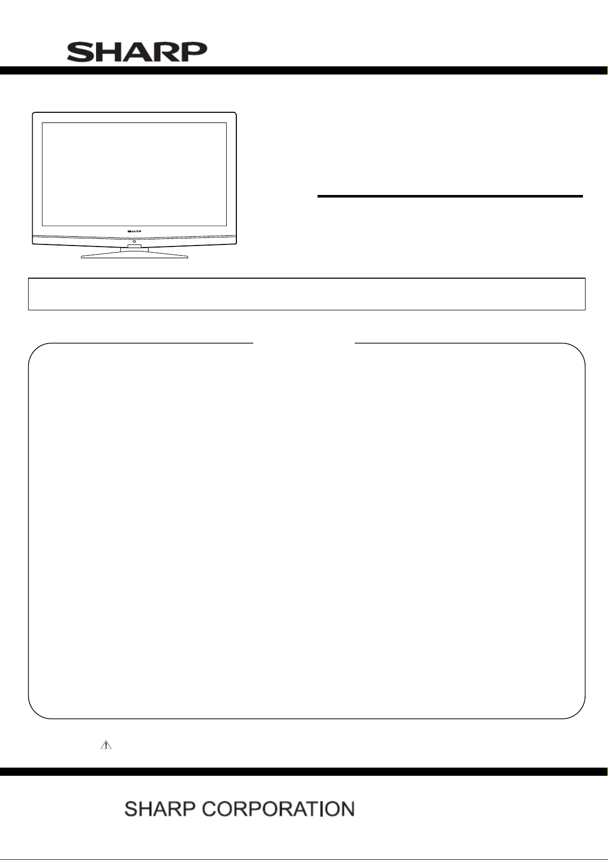
LC-32SH25E
SERVICE MANUAL
No. SX8T4LC32SH25
LCD COLOUR TELEVISION
MODELS
In the interests of user-safety (Required by safety regulations in some countries) the set should be restored to its original condition and only parts identical to those specified should be used.
SAFETY PRECAUTION
IMPORTANT SERVICE SAFETY PRE-
CAUTION ................................................. ... ........2
Precautions for using lead-free solder ......….......3
CHAPTER 1. OPERATION MANUAL
[1] SPECIFICATIONS ..................................................4
[2] OPERATION MANUAL ...........................................5
[3] DIMENSIONS .......................................................10
CHAPTER 2. REMOVING OF MAJOR PARTS
[1] REMOVING OF MAJOR PARTS ..........................11
CHAPTER 3. ADJUSTMENT PROCEDURE
[1] ADJUSTMENT PROCEDURE .............................16
[2] SERVICE MODE ..................................................21
[3]
SOFTWARE UPGRADE PROCEDURE...............22
CHAPTER 4. TROUBLESHOOTING TABLE
[1] TROUBLESHOOTING TABLE..............................26
CHAPTER 5. MAJOR IC INFORMATIONS
[1] MAJOR IC INFORMATIONS.................................39
CHAPTER 6. BLOCK DIAGRAM/WIRING DIAGRAM
[1] VIDEO & AUDIO BLOCK DIAGRAM ...................59
Parts marked with " " are important for maintaining the safety of the set. Be sure to replace these parts with specified ones for maintaining the
safety and performance of the set.
CONTENTS
[2] POWER MANAGEMENT BLOCK DIAGRAM ......60
[3] I2C and RS232 BLOCK DIAGRAM .......................61
[4] WIRING DIAGRAM ...............................................62
CHAPTER 7. PRINTED WIRING BOARD
[1] MAIN UNIT PRINTED WIRING BOARD ...............63
[2] POWER UNIT PRINTED WIRING BOARD ..........65
[3] KEY UNIT PRINTED WIRING BOARD .................67
[4] IR UNIT PRINTED WIRING BOARD ....................68
CHAPTER 8. SCHEMATIC DIAGRAM
[1] MAIN SCHEMATIC DIAGRAM ............................69
[2] POWER SCHEMATIC DIAGRAM .......................83
[3] KEY SCHEMATIC DIAGRAM .............................84
[4] IR SCHEMATIC DIAGRAM .................................85
CHAPTER 9. Parts Guide
[1] SPARE PARTS LIST.............................................86
[2] CABINET PARTS ................................................108
[3] SUPPLIED ACCESSOORIES..............................110
[4] PACKING PARTS................................................111
LC-32SH25E
This document has been published to be used for
after sales service only.
The contents are subject to change without notice.
1
Page 2
LC-32SH25E
SAFETY PRECAUTION
IMPORTANT SERVICE SAFETY PRECAUTION
■ Service work should be performed only by qualified service technicians who are thoroughly familiar with all safety checks and the
servicing guidelines which follow:
■ WARNING
1. For continued safety, no modification of any circuit should be
attempted.
2. Disconnect AC power before servicing.
CAUTION:
FOR CONTINUED PROTECTION AGAINST A
RISK OF FIRE REPLACE ONLY WITH SAME
TYPE FUSE.
42" F901 (T6.3AH/250V)
26"/32" F901 (T5AH/250V)
■
BEFORE RETURNING THE RECEIVER
(Fire & Shock Hazard)
Before returning the receiver to the user, perform the following
safety checks:
3. Inspect all lead dress to make certain that leads are not pinched,
and check that hardware is not lodged between the chassis and
other metal parts in the receiver.
4. Inspect all protective devices such as non-metallic control knobs,
insulation materials, cabinet backs, adjustment and compartment
covers or shields, isolation resistor-capacitor networks, mechanical
insulators, etc.
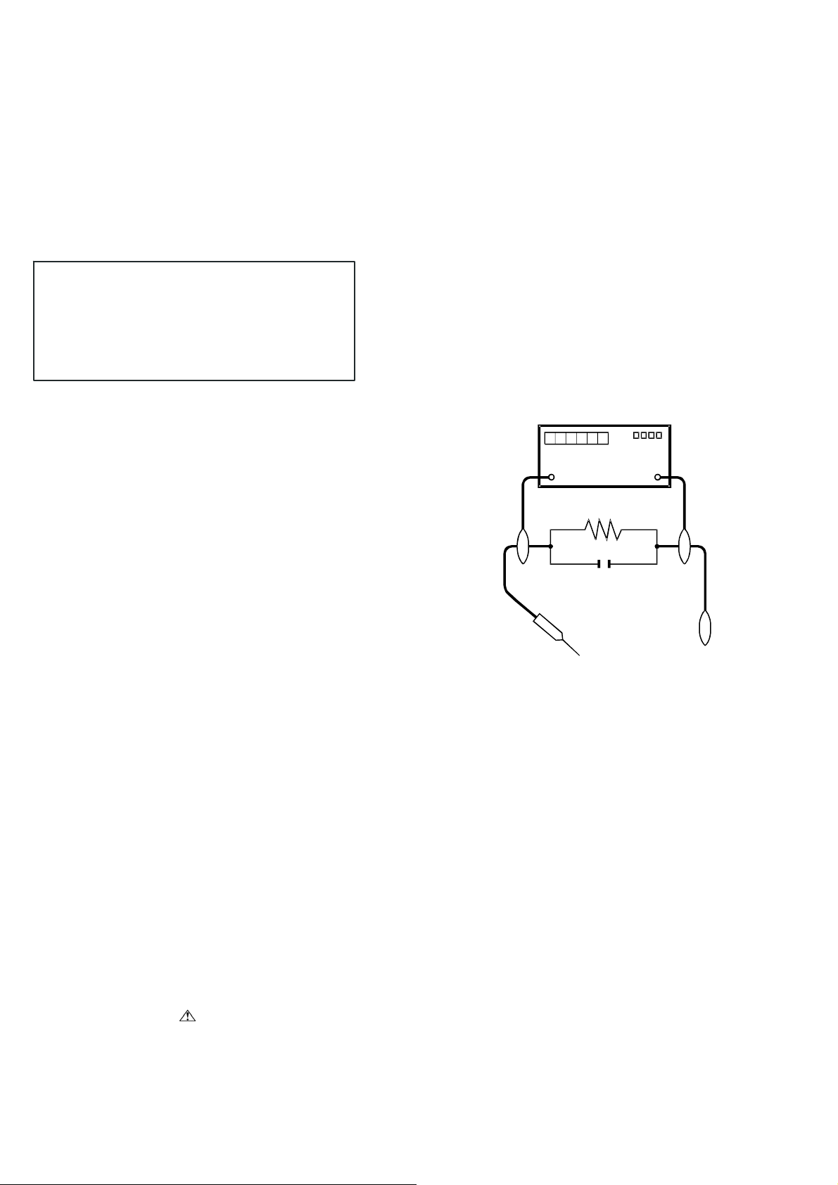
5. To be sure that no shock hazard exists, check for leakage current in
the following manner.
• Plug the AC cord directly into a 220~240 volt AC outlet.
• Using two clip leads, connect a 1.5k ohm, 10 watt resistor paralleled
by a 0.15µF capacitor in series with all exposed metal cabinet
parts and a known earth ground, such as electrical conduit or
electrical ground connected to an earth ground.
//////////////////////////////////////////////////////////////////////////////////////////////////////////////////////////////////////////////////////////////////////////////////////////////////////////////////////////////////////////////////
SAFETY NOTICE
Many electrical and mechanical parts in LCD color television have
special safety-related characteristics.
These characteristics are often not evident from visual inspection,
nor
can protection afforded by them be necessarily increased by using
replacement components rated for higher voltage, wattage, etc.
Replacement parts which have these special safety characteristics
are identified in this manual; electrical components having such
features are identified by “ ” and shaded areas in the Replacement
Parts List and Schematic Diagrams.
//////////////////////////////////////////////////////////////////////////////////////////////////////////////////////////////////////////////////////////////////////////////////////////////////////////////////////////////////////////////////
• Use an AC voltmeter having with 5000 ohm per volt, or higher, sensitivity or measure the AC voltage drop across the resistor.
• Connect the resistor connection to all exposed metal parts having a
return to the chassis (antenna, metal cabinet, screw heads, knobs
and control shafts, escutcheon, etc.) and measure the AC voltage
drop across the resistor.
All checks must be repeated with the AC cord plug connection
reversed. (If necessary, a nonpolarized adaptor plug must be used
only for the purpose of completing these checks.)
Any reading of 1.05 V peak (this corresponds to 0.7 mA peak AC.)
or more is excessive and indicates a potential shock hazard which
must be corrected before returning the monitor to the owner.
DVM
AC SCALE
1.5k ohm
10W
0.15 µF
TEST PROBE
TO EXPOSED
METAL PARTS
CONNECT TO KNOWN
EARTH GROUND
For continued protection, replacement parts must be identical to those
used in the original circuit.
The use of a substitute replacement parts which do not have the same
safety characteristics as the factory recommended replacement parts
shown in this service manual, may create shock, fire or other hazards.
2
Page 3

LC-32SH25E
Precautions for using lead-free solder
Using lead-free wire solder
• When fixing the PWB soldered with the lead-free solder, apply lead-free wire solder. Repairing with conventional lead wire solder may cause
damage or accident due to cracks.
As the melting point of lead-free solder (Sn-Ag-Cu) is higher than the lead wire solder by 40 °C, we recommend you to use a dedicated soldering
bit, if you are not familiar with how to obtain lead-free wire solder or soldering bit, contact our service station or service branch in your area.
Soldering
• As the melting point of lead-free solder (Sn-Ag-Cu) is about 220 °C which is higher than the conventional lead solder by 40 °C, and as it has
poor solder wettability, you may be apt to keep the soldering bit in contact with the PWB for extended period of time. However, Since the land
may be peeled off or the maximum heat-resistance temperature of parts may be exceeded, remove the bit from the PWB as soon as you
confirm the steady soldering condition.
Lead-free solder contains more tin, and the end of the soldering bit may be easily corroded. Make sure to turn on and off the power of the bit as
required.
If a different type of solder stays on the tip of the soldering bit, it is alloyed with lead-free solder. Clean the bit after every use of it.
When the tip of the soldering bit is blackened during use, file it with steel wool or fine sandpaper.
• Be careful when replacing parts with polarity indication on the PWB silk.
3
Page 4
LC-32SH25E
CHAPTER 1. OPERATION MANUAL
[1] SPECIFICATIONS
Specification
Item
LCD panel 32” diagonal
Number of dots
Video Colour System
TV-Standard
TV Function
Backlight life 60,000 hours (at Backlight Standard position)
Viewing angles H : 176° V : 176°
Audio amplifier 5W X 2
Speaker (100 mm X 30 mm) X 2
Rear
Side
OSD language
Power Requirement
Power Consumption
Receiving
Channel
TV-Tuning System Auto Preset 999 ch, Auto Label, Auto Sort
STEREO/BILINGUAL NICAM/A2
Antenna
RS-232C D-Sub 3 pin male connector
SCART 1 SCART (AV input, Y/C input, RGB input, TV output-analogue only)
SCART 2 SCART (AV input, Y/C input, monitor output (analogue source - RF, SCART 1, SIDE AV) )
PC IN VGA pin (AV input), Ø 3.5mm jack (Audio output)
Component Y/Pb(Cb)/Pr(Cr), RCA pin (L/R)
SPDIF Digital audio output
AUDIO OUT RCA pin (L/R)
HDMI 1
HDMI 2
C. I. (Common Interface) EN50221, R206001
Headphones Ø 3.5mm jack (Audio output)
AV IN RCA pin (AV input) , RCA pin (L/R), S-VIDEO (Y/C input)
USB
HDMI 3
Analogue
Digital
VHF/UHF ATV : IRA-E69, DVB-T : E5-E69
CATV S-band, S1–S41ch
32” LCD Colour TV
Model: LC-32SH25E
3,147,264 dots
(1366 X 768 X 3 dots)
PAL/SECAM/NTSC 3.58/NTSC 4.43/PAL 60
CCIR (B/G, I, D/K, L/L’)
DVB-T (2K/8K OFDM)
UHF/VHF 75 Ω
For service use only
Bulgarian, Croatian, Czech, Danish, Dutch, English, Finnish, French, German, Greek, Hungarian,
Italian, Norwegian, Polish, Portuguese, Romanian, Russian, Serbian, Slovak, Slovene, Spanish,
Swedish, Turkish
AC 220–240 V, 50 Hz
150 W (Standby<1W)
(Method IEC60107)
,
Weight
Operating temperature 0°C to + 40°C
• As a part of policy of continuous improvement, SHARP reserves the righ t to make design and specification changes for product improvement
without prior notice. The performance specification figures indicated are nominal values of production units. There may be some deviations
from these values in individual units.
10.7 kg (Without stand),
12.5 kg (With stand)
4
Page 5
[2] OPERATION MANUAL
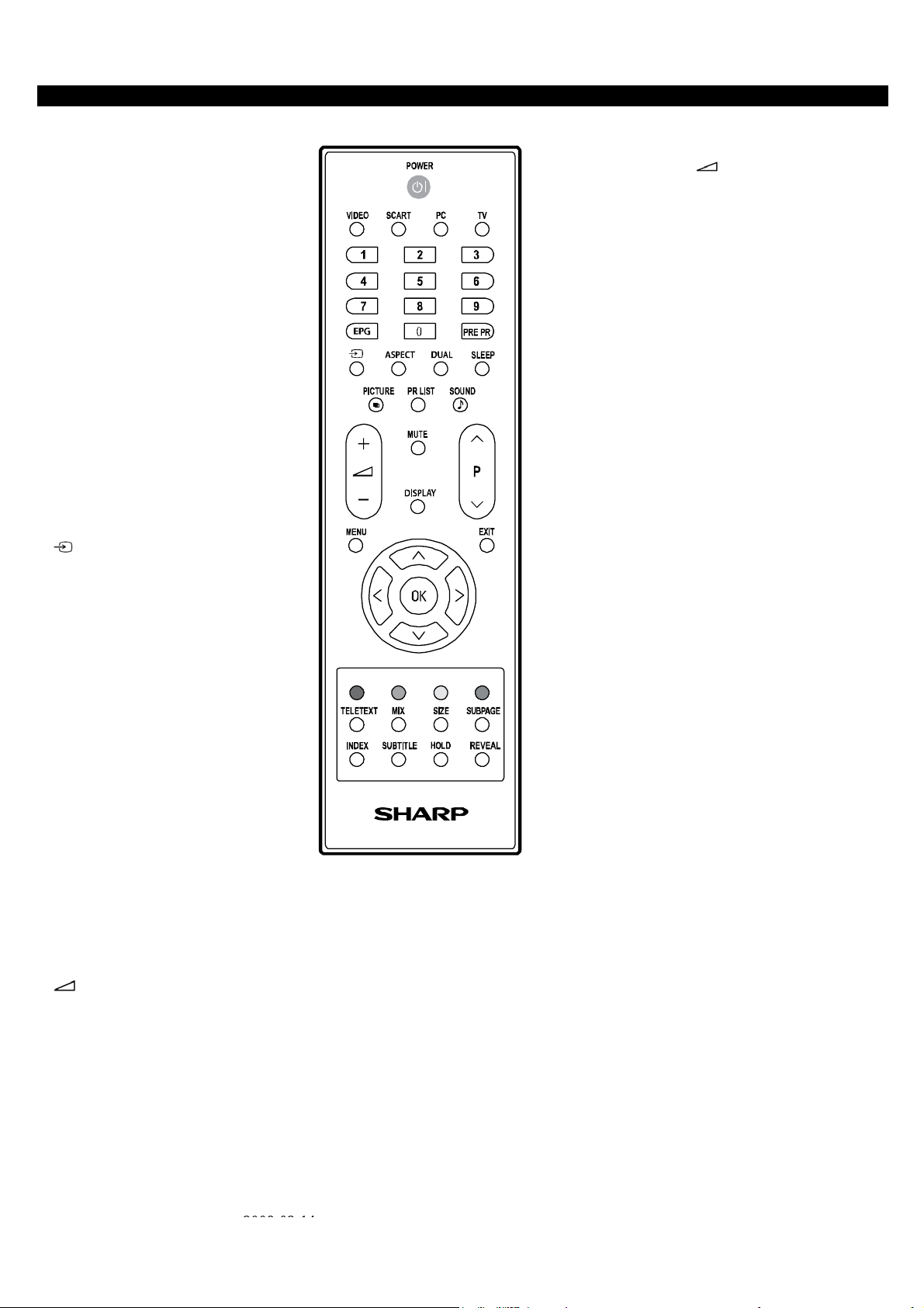
Remote control unit
POWER
Press to turn the LCD TV on or enter
standby mode.
VIDEO
Press this key you could select YPbPr, Side
AV, HDMI 1, HDMI 2, HDMI 3.
SCART
Press this key you could select
SCART 1, SCART 2.
PC
Press to direct to the PC mode.
TV
Press to direct to the TV mode.
0-9 DIGIT BUTTONS
To select a TV channel directly.
EPG
Press this button to display electronic
program guide in TV mode.
PRE PR
To display the previous selected TV channel.
(INPUT SOURCE)
Select an input source.
ASPECT
Change the aspect ratio; please refer to
Picture format section.
DUAL
Select MONO, STEREO, DUAL 1 and DUAL
2 for ATV channel. Select Audio language for
DTV channel.
SLEEP
Press to turn the LCD TV off within an
amount of time. (5-180 minutes.)
PICTURE
Press to set the LCD TV to a predefined
picture setting.
User / Cinema / Sport / Vivid / Hi-Bright
PR LIST
Press to display a list of channels. Then
press Red button to select the Digital or
Analogue channel list.
SOUND
Press to set the LCD TV to a predefined
sound setting.
Off / Rock / Pop / Live / Dance / Techno /
Classic / Soft
(+/-)
Press to adjust the volume.
P(∧/
)
∨
Press to select the channel.
LC-32SH25E
MUTE
Press to toggle audio on and off.
You can also press (+/-) VOL to
restore the previous volume level.
DISPLAY
Press to display the current signal
status, including input source/
channel audio mode.
MENU
Press to activate the LCD TV OSD.
Press again to exit the LCD TV
OSD.
EXIT
Press to exit LCD TV OSD.
OK
Press to activate a setting.
<>
∧∨
Press ∧∨<>
to navigate and confirm your selection.
R/G/Y/B (Colour Button)
Press buttons to select the pictures with
various colours of text. Different channels
display different functions.•
TELETEXT
Press this button to activate Teletext. Press
again to turn off Teletext.
MIX
Press this button to activate Teletext with TV.
SIZE
Press this button to change the font size: Full
screen, Top half and Bottom half.
SUBPAGE
To select the subpage when the current page
contains subpage(s).
INDEX
Press this button to return to page 100 or the
index page; and then press 0 to 9. The teletext
page will be numbered and added to the page
you select or the secondary item.
SUBTITLE
For DTV, press it to select subtitle setting.
off / on / on during mute
For ATV, please activate Teletext to select
subtitle page.
HOLD
Press this button to stop the scrolling of pages.
The text decoder stops receiving data.
REVEAL
Reveal hidden information such as answers to
a quiz.
2008-03-14
5
Page 6
LC-32SH25E
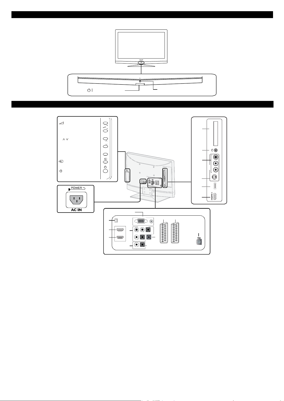
TV (Front view)
TV (Rear view)
(+/-)
Volume buttons
P
( )
/
Programme [channel] buttons
MENU
button
(INPUT SOURCE) bu tton
(Power) button
1
1 Power connector
2 SERVICE socket
3 HDMI 1
4 HDMI 2
5 PC IN (VGA/AUDIO)
6 Component Video and L/R Audio input
7 SPDIF Output (Digital audio out)
8 AV L/R Audio Output
9 SCART 1 (CVBS Tuner out)
10 SCART 2 (CVBS Monitor out)
11 Tuner Input
12 COMMON INTERFACE slot
13 Earphone Output
14 Composite ( AV IN, AV/LR)
15 S-Video
16 SERVICE socket(For LC-32SH25E)
17 HDMI 3
(Standby/On) indicator
P
MENU
2
3
4
SERVICE
HDMI1
HDMI2
5
6
YPbPr
LRSPDIF OUT
8
L
PC IN
VGA
COMPONENT
R
6
AUDIO
7
AUDIO OU T
Remote control sensor
9
10
SCART1 SCART2
12
13
14
15
16
17
11
Page 7
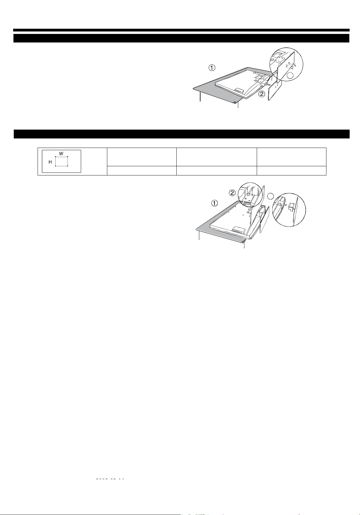
Preparation
Mount the TV Stand
1. Put the TV face down on a safe surface that
is covered by a soft and smooth cloth.
2. Adjust the TV stand to the base column.
3. Fasten 4 screws.
Wall mounting
LC-32SH25E
3
TV screen size
( inches)
1. Put the TV face down on a safe surface that is
covered by a soft and smooth cloth.
2. Unscrew the 4 bolts that fasten the base
column to the TV by using a cross-head
screwdriver. (not supplide)
3. Detach the stand from the bottom of the TV.
32” 200 x 200 mm Metric 6 x 10 mm
VESA-compatible wall bracket
(millimeters) (W x H)
Screw type
3
2008-03-14
7
Page 8
LC-32SH25E
preparation
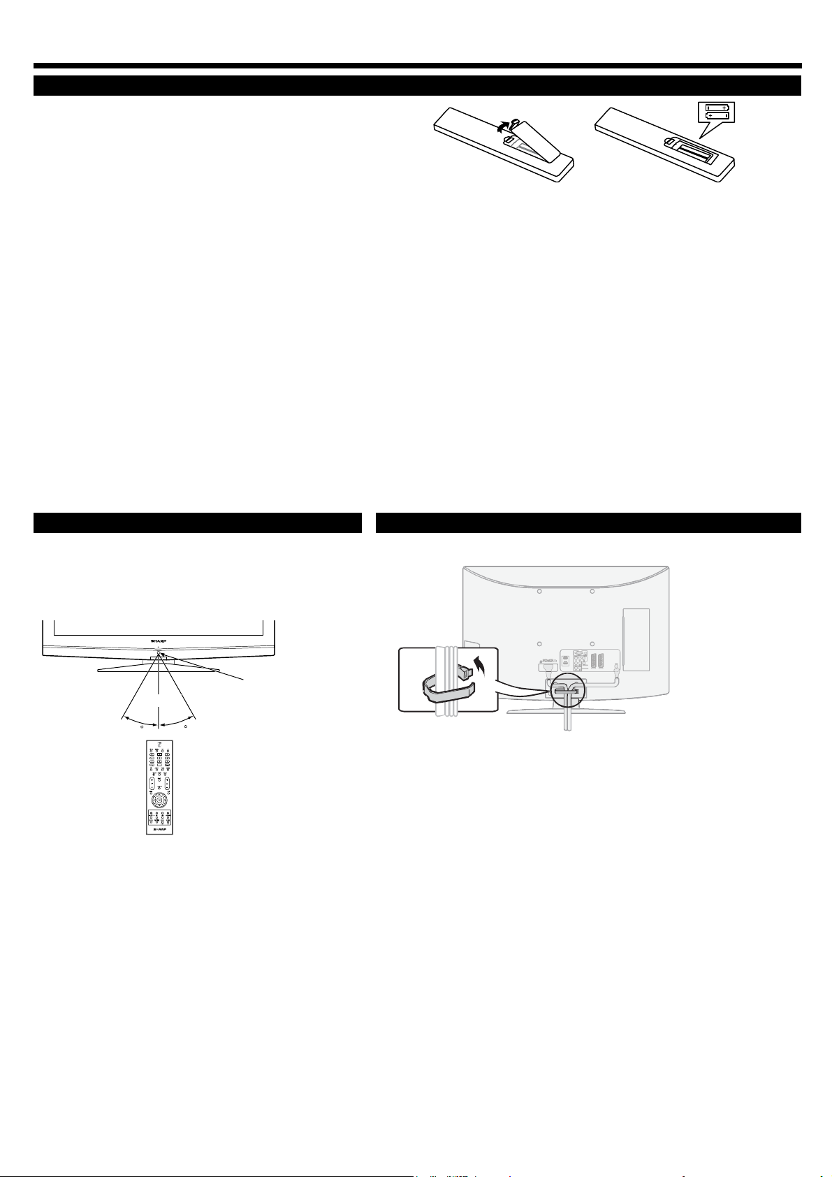
Installation of batteries
1. insert two AAA batteries into Remote control.
Make sure (+) and (-) are facing the proper
direction.
2. Replace the cover.
NOTE
• If the remote control will not to be used for a long
time, remove the batteries to avoid remote control damage.
CAUTION
Improper use of batteries can result in chemical leakage or explosion. Be sure to follow the instructions below.
• Do not mix batteries of different types. Different types of batteries have different characteristics.
• Do not mix old and new batteries. Mixing old and new batteries can shorten the life of new batteries or cause
chemical leakage in old batteries.
• Remove batteries as soon as they have worn out. Chemicals that leak from batteries can cause a rash. If you find
any chemical leakage, wipe thoroughly with a cloth.
• The batteries supplied with this product may have a shorter life expectancy due to storage conditions.
• If you will not be using the remote control unit for an extended period of time, remove the batteries from it.
Note on disposing batteries:
The batteries provided contain no harmful materials such as cadmium, lead or mercury.
Regulations concerning used batteries stipulate that batteries may no longer be thrown out with the household
Rubbish. Deposit any used batteries free of charge into the designated collection containers set up at commercial
Businesses.
Using the remote control unit Bundling the cables
Use the remote control unit by pointing it towards the
remote control sensor. Objects between the remote
control unit and sensor may prevent proper operation.
5m
30
Remote control sensor
30
8
Page 9
LC-32SH25E
Appendix
troubleshooting
problem possible Solution
No picture 1. Connect power cord correctly.
2. Turn on power.
3. Connect signal cable correctly.
4. Press any button on the LCD TV.
Abnormal colours Connect signal cable correctly.
Twisted picture 1. Connect signal cable correctly.
2. Please use compatible signal.
Picture too dark Adjust brightness and contrast.
Audio only, no images 1. Please check if input signal is connected correctly.
Picture only, no audio 1. Connect signal cable correctly.
Cannot use remote control 1. Please change battery.
Cannot receive sufficient channels
through antenna
No colours Please adjust the colour setup
Blinking picture accompanied by ghost
image
Broken lines or segments
Certain TV channels are blocked (Hope to
acquire some channels)
Overlapping images or ghost images Please use multi-directional outdoor antenna. (If your TV is subject to the influence of nearby mountains or
Cannot use a function If the item you choose turns gray, that item cannot be selected.
Cannot receive programs Please use the Update scan method to add the channels not included in memory.
1. When a lamp in LCD panel is broken and the
protector circuit in inverter operates and we
tune on the this set, LED keep red? or Green?
2. Service man only change the lamp in LCD
panel?
Cautions regarding use in high and low temperature environments
• When the unit is used in a low temperature space (e.g. room, office), the picture may leave trails or appear slightly delayed. This
is not a malfunction, and the unit will recover when the temperature returns to normal.
• Do not leave the unit in a hot or cold location. Also, do not leave the unit in a location exposed to direct sunlight or near a
heater, as this may cause the cabinet to deform and the LCD panel to malfunction.
• Storage temperature: +5°C to +35°C.
information on the software license for this product
Software composition
The software included in this product is comprised of various software components whose individual copyrights are held by SHARP or by third parties.
Software developed by SHarp and open source software
The copyrights for the software components and various relevant documents included with this product that were developed or written by SHARP are
owned by SHARP and are protected by the Copyright Act, international treaties, and other relevant laws. This product also makes use of freely
distributed software and software components whose copyrights are held by third parties. These include software components covered by a GNU
General Public License (hereafter GPL), a GNU Lesser General Public License (hereafter LGPL) or other license Agreement.
obtaining source code
Some of the open source software licensors require the distributor to provide the source code with the executable software components. GPL and
LGPL include similar requirements. For information on obtaining the source code for the open source software and for obtaining the GPL, LGPL, and
other license agreement information, visit the following website:
2. TV-RF signal must not be lower than 50dB.
2. Adjust volume to proper level.
3. Connect audio signal cable correctly.
4. TV-RF signal must not be lower than 50dB.
2. Turn off power for 10 seconds; and then restart power.
Please use the Channel scan function to increase the number of channels not included in memory.
1. Check the connection of antenna/signal cable.
2. Check if channel is in play mode.
3. Press signal source and change input mode.
Adjust antenna.
Keep the TV away from noise sources, such as automobiles, neon lights, and hair dryers.
Please use the Update scan method to add the channels not included in memory
buildings).
1. If the lamp(s) is(are) broken, panel inverter will not kick on the lamps, so TV set phenomena will be "no picture
on display."
But the TV system is still working, that is the RC can also control LED.
When AC power on, the LED will keep last status and when use RC DC power on, the LED will keep green light.
2. The failed panel should be sent back to Panel maker (CMO) via RMA process.
Panel maker (CMO) will not rework the lamps at customer's side since the repaired panel should be checked
through regular inspection flow to secure the quality.
http://www.sharp-eu.com/gpl/
We are unable to answer any questions about the source code for the open source software. The source code for the software components whose
copyrights are held by SHARP is not distributed.
acknowledgements
The following open source software components are included in this product:
•linuxkernel•modutils•glibc•zlib•libpng
2008-03-14
9
Page 10
LC-32SH25E
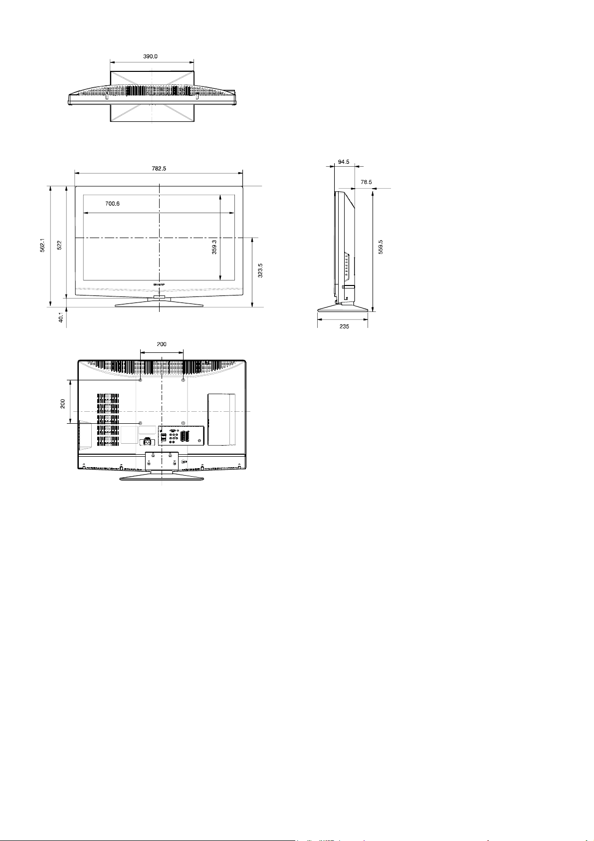
[3] DIMENSIONS
10
Page 11
CHAPTER 2. REMOVING OF MAJOR PARTS
[2] REMOVING OF MAJOR PARTS(LC-32SH25)
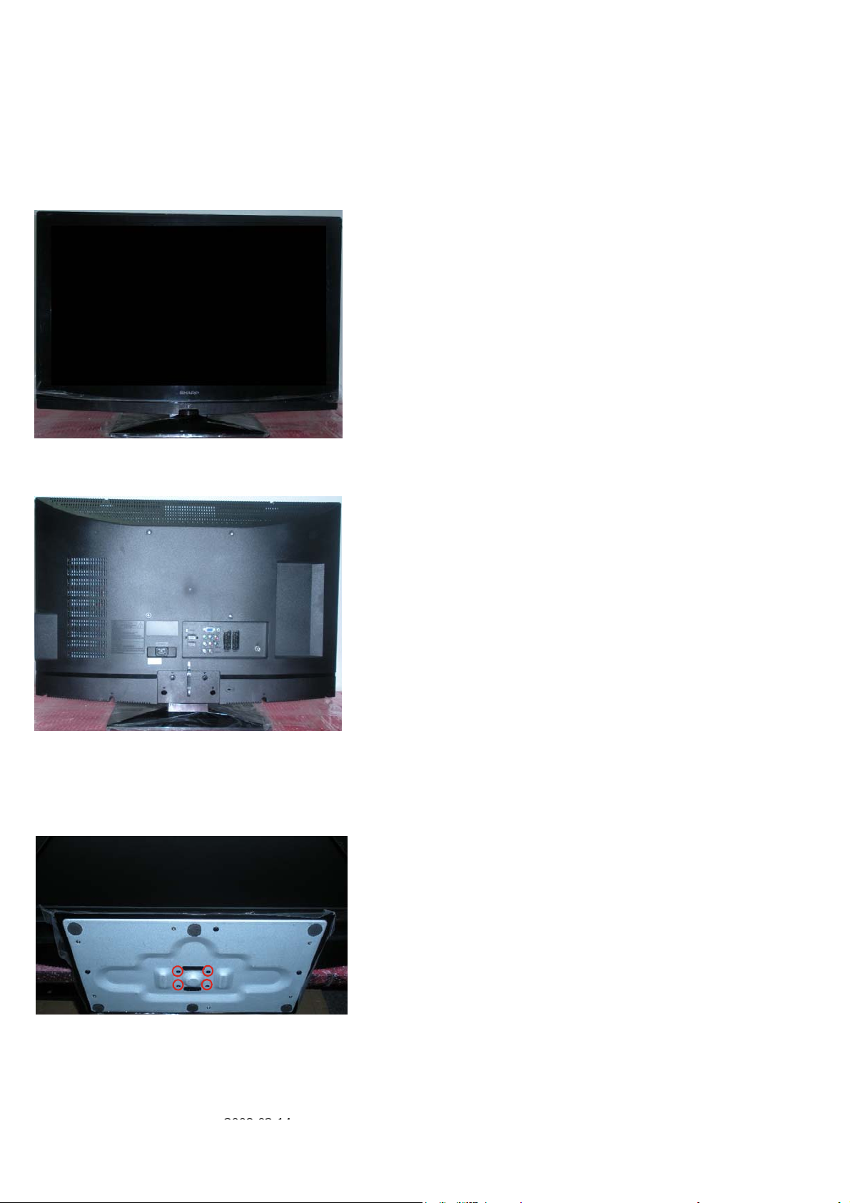
1. Assy/Panel Removal
Notes: Please put your machine on soft material to avoid to scrape panel when you disassemble it.
Front view
Fig.1
Back view
LC-32SH25E
Fig.2
Step 1. Remove the Base Assy.
1. Remove the base as Fig.3.
Remove the 4 screws as Fig.3 and pull out the base as Fig.4
Fig.3
2008-03-14
11
Page 12
LC-32SH25E
Fig.4
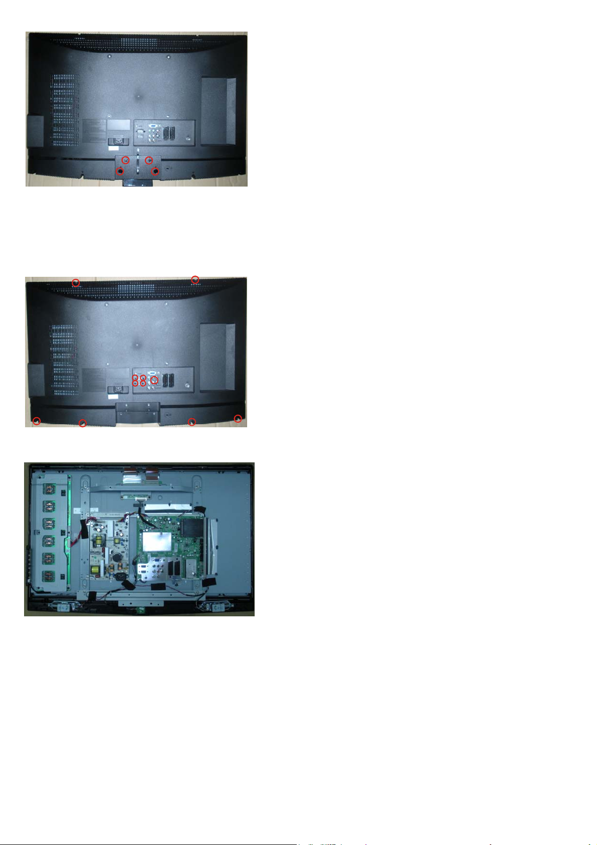
2. Remove the 4 screws. Detach the BASE STAND as Fig.5.
Step 2. Remove the REAR COVER Assy.
1. Remove the 11 screws. Detach the REAR COVER as Fig.5.
Fig.5
Step 3. Remove the Main, Power, IR, Key board and the Speakers.
Fig.6
1. Remove the 6 screws and disconnect 4 cables. Detach the Main board as Fig.7 and Fig.8.
12
Page 13
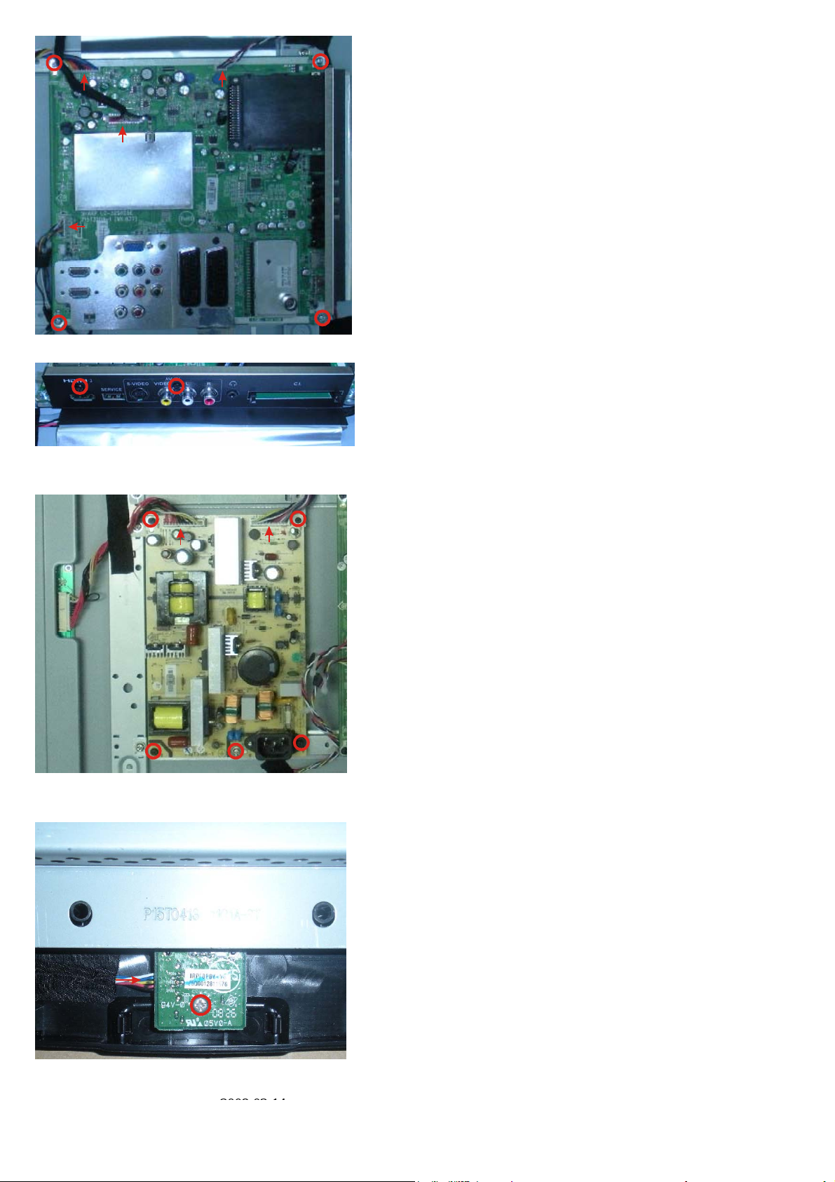
Fig.7
LC-32SH25E
Fig.8
2. Remove the 5 screws and disconnect 2 cables. Detach the Power board as Fig.9.
Fig.9
3. Remove the 1 screw and disconnect 1 cable. Detach the IR board as Fig.10.
Fig.10
4. Disconnect 1 cable. Detach the Key board as Fig.11.
2008-03-14
13
Page 14
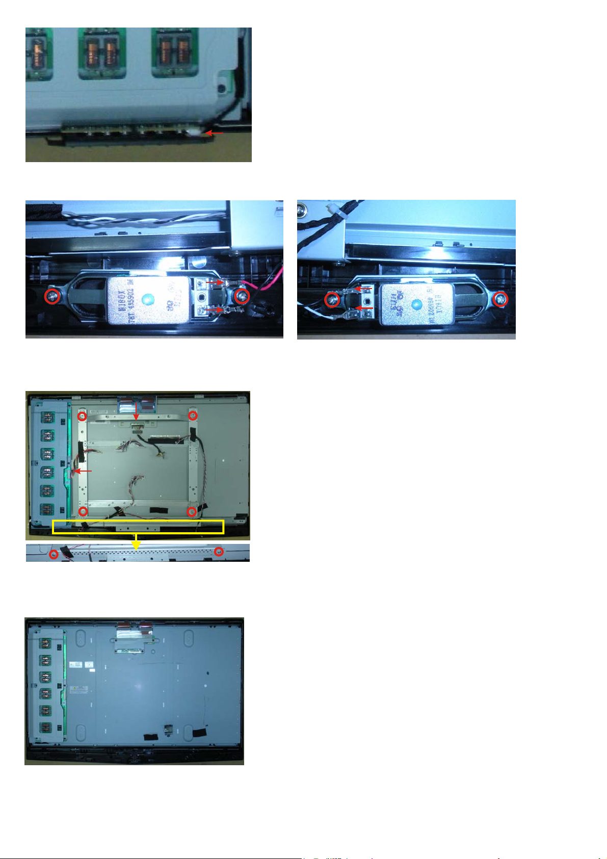
LC-32SH25E
Fig.11
5. Remove the 4 screws and disconnect 4 cables. Detach the Speakers as Fig.12 and Fig.13.
Fig.12 Fig.13
Step 4. Remove the Metal Frame.
1. Remove the 6 screws and disconnect 2 cables. Detach the Metal Frame as Fig.14.
Fig.14
Step 5. Remove the Bezel Assy.
1. Remove the Bezel Assy as Fig.15
Fig.15
2. The below picture is panel as Fig.16.
14
Page 15
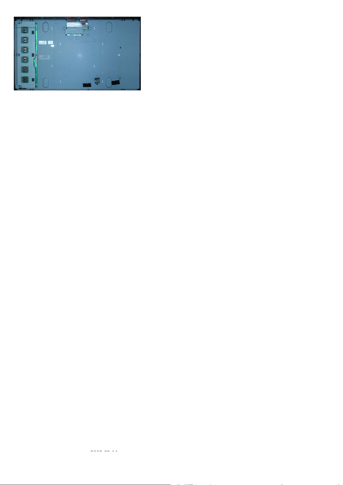
Fig.16
2. Set Re-assembly
To re-assemble the whole set, execute all processes in reverse order.
Notes:
a. While re-assembling, make sure that all cables are placed and connected in their original position.
b. Pay special attention not to damage the EMC foams at the SSB shielding. Check that EMC foams are put
correctly on their places.
LC-32SH25E
2008-03-14
15
Page 16

LC-32SH25E
CHAPTER 3. ADJUSTMENT PROCEDURE
PROCEDURE
[1] ADJUSTMENT PROCEDURE
1. OSD Menu
OSD tree - As following
• TV
Digital Europe OSD tree-TV Remark
OSD Layer
1 2 3 4 5 6
Picture
Contrast slider
Brightness slider
Color slider
Sharpness slider
Tint
Color temperature
Cool
Picture format Automatic
Noise Reduction Off
On
Sound
Virtual surround Off
On
Dual I-II Dual I
Dual II
Mono/Stereo Mono
Stereo
Auto volume leveling Off
On
Smart Picture
Settings
Sound mode
Volume-visually
impaired
Audio language
User
Cinema
Sport
Vivid
Hi-bright
slider
Normal
Warm
Super zoom
4:3
Movie expand 14:9
Movie expand 16:9
Wide screen
Subtitle zoom
Bass slider
Treble slider
Balance slider
Off
Rock
Pop
Live
Dance
Techno
Classic
Soft
slider
Broadcsted list of audio languages
16
Page 17
Features Timer
Stop time Timer Off
On
Sleeptimer slider
Auto lock Lock program
Change code
Clear all Start now
Parental rating None
Age 4~18
X-rated(Spain)
Subtitle Off
On
On during mute
Subtitle language Broadcsted list of audio languages
Common interface
Installation
Preferred audio language Basque
Bulgarian
Catalan
Croatian
Czech
Danish
Dutch
English
Finnish
Language
Clock
Start time
Menu language Български
Česky
Dansk
Deutsch
English
Hrvatski
Italiano
magyar
Nederlands
Norsk
Polski
Română
Svenska
Türkçe
Time zone
Time
Timer Off
On
(Channel
number…)
Please enter your
current PIN.
Ελληνικά
Español
Français
Português
Русский
Slovenský
Slovenščina
Srpski
Suomi
GMT +x:xx
GMT -x:xx
As broadcaster
Auto
synchronization
Date
Time
On
Off
20xx/xx/xx
xx:xx:xx
2008-03-14
(When CAM
inserted)
LC-32SH25E
17
Page 18

LC-32SH25E
French
Gaelic
Galician
German
Greek
Hungarian
Italian
Norwegian
Polish
Portuguese
Romanian
Russian
Serbian
Slovak
Slovenian
Spanish
Swedish
Turkish
Welsh
Preferred subtitle language Basque
Bulgarian
Catalan
Croatian
Czech
Danish
Dutch
English
Finnish
French
Gaelic
Galician
German
Greek
Hungarian
Italian
Norwegian
Polish
Portuguese
Romanian
Russian
Serbian
Slovak
Slovenian
Spanish
Swedish
Turkish
Welsh
Hearing impaired Off
On
Audio description Off
On
Country France
Channel installation Automatic installation Start now
Installation update Start now
Digital: Test reception 000.00 MHz Start Network name:
Status:
scanning…
Digital channels
found:
Analoguel
channels found:
Status:
scanning…
Signal
quality:Good/Poor
18
Page 19
Signal strength:
Analog: Manual installation System West EU
East EU
UK
France
Search 000 MHz
Fine tune 000.00 MHz
Rearrange
Source labels
SCART 1 DVD
SCART 2 Blu-ray
PC HDD/DVDR
HDMI 1 HD rec.
HDMI 2 Game
HDMI 3 VCR
PC
Digital STB
HD dig STB
Other
Decoder (Channel numbers…)
Current software info
Factory reset Start now
YPbPr
Side AV No label
Store current
channel Store
Store as new
channel Store
(Channel
numbers…)
Rename,reshuffle
• PC
LC-32SH25E
Digital Europe OSD tree-PC Remark
OSD Layer
1 2 3 4 5
Picture Contrast slider
Brightness slider
Colour Temperature Normal
Warm
Cool
Picture format
Sound Incredible surround Off
On
Picture
adjustment
Factory
reset Start now
Auto adjust
Manual adjust
Clock
Horizontal
Vertical
4:3
Wide screen
Start
Phase slider
slider
slider
slider
2008-03-14
19
Page 20
LC-32SH25E
2. Picture check
1) WHITE-D adjustment
General set-up :
Equipment Requirements: Minolta CA-210 or Equivalent Color analyzer Chroma 2250 or equivalent PC signal generator
input requirements:
Input Signal Type : PC VGA signal
1280 X 1024/60Hz PC mode with ”5 white block” pattern. (see pattern-1)
Input Signal Strength : 0.7 Vp-p linear voltage.
Input Injection Point : PC D-SUB input
Pattern-1
Alignment method:
Initial Set-up:
1>. Select source as “PC”.
2>. Set Contrast = 50 (Sharp) and Brightness=50 (Sharp) , at normal menu mode.
3>. Apply “5 white block”(pattern-1) pattern b y VGA pattern generator.
4>. Enter factory mode menu: press MENU + Numeric keys “062596” + MENU key (FAC mode menu). Then select “Factory” item.
Alignment:
1>. At FAC mode menu, select AUTO_COLOR item. Then press “OK” key to adjust ADC_GAIN_R, ADC_GAIN_G, ADC_GAIN_B and ADC_OFFSET_R,
ADC_OFFSET_G, ADC_OFFSET_B. Then store those values to NVM.
2>. Apply Flat80 pattern (80% white pattern).
3>. Set color temperature to “NORMAL”.
4>. At FAC mode menu, adjust the CLR TEMP R
store those values to NVM
5>. Set color temperature to “COOL”.
6>. At FAC mode menu, adjust the CLR TEMP R
those values to NVM
7>. Set color temperature to “WARM”.
8>. At FAC mode menu, adjust the CLR TEMP R
those values to NVM
Color temperature Normal/Warm/Cool (x, y) co-ordinates specification:
Picture Mode x y
Normal (9000oK) 0.289±0.003 0.291±0.003
Cool (12000oK) 0.272±0.003 0.277±0.003
Warm (6500oK) 0.314±0.003 0.319±0.003
Table 5: Reading with Minolta CA-210.
Note:
1>. Use Minolta CA-210 for color coordinates and luminance check.
2>. Befor adjusting,all colour analyzers (CA-210) should be coordinates with a same reference TV set.
3>. Luminance > 400 cd/m
2
in the center of the screen when Brightness control at 100; Contrast control at 100 for Sharp 32” panels.
, CLR TEMP G, CLR TEMP B values to meet “NORMAL” color coordinates specification below. Then
, CLR TEMP G, CLR TEMP B values to meet “COOL” color coordinates specification below. Then store
, CLR TEMP G, CLR TEMP B values to meet “WARM” color coordinates specification below. Then store
20
Page 21
LC-32SH25E
[2] SERVICE MODE
Enter factory mode menu: press MENU + Numeric keys “062596” + MENU key (FAC mode menu).Then select “Factory”
item.
2008-03-14
21
Page 22
LC-32SH25E
[3] SOFTWARE UPGRADE PROCEDURE
Environment Setup
Before you start to write the code, we suggest you setup the environment first. This chapter lists the setup requirements and guides you to setup and test
your development environment.
1.1 Connect to ISP Board to upgrade the software firmware.
Use USB port connecting PC & MT536x Board via ISP board(Code number: 9JR9900000099(715G537XL2)).
To P C U S B port
Example: PC Connected to system board service port ( From USB to RS232).
To system board
service port
1. Unzip USB2COM Driver.zip to C:\
PL-2303 Driver Installer.rar
I. PL-2303 Driver Installer.exe
II. Double click exe file to install driver
2. Use MTK_Tools to download .bin file. (Ex: SHARP_LC_32SH25E__Vxx.xx_image.bin)
3. Make sure the Type “MTK539X” && “USB Baud Rate 115200x8” && Load the correct “bin” file.
Detailed operation sequence listed as follows.
Load .bin file on the Linux system or on the local Windows file system(Ex: SHARP_LC_32SH25E__Vxx.xx_image.bin) & Set Bridge & Auto Set Flash
BaudRate.
mtktool_mt5391.rar
22
Page 23
BaudRate.
LC-32SH25E
4. Set COM port resource that used by USB Port.
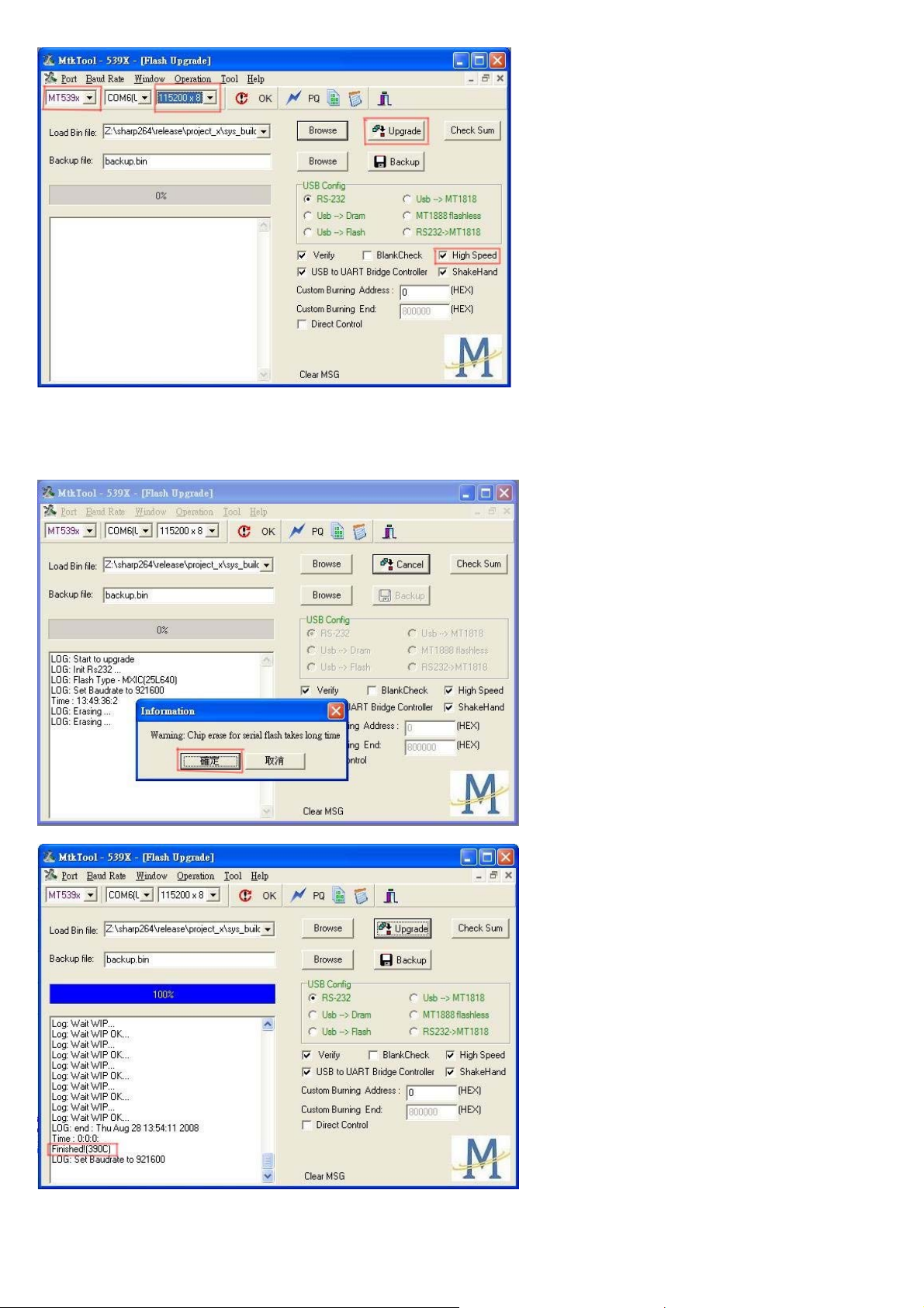
5. Set Baud rate 115200x8 & High speed item Enable. & MT539x.
2008-03-14
23
Page 24
LC-32SH25E
6. Push “Upgrade” button. (Waiting for “Finished!” message.)
Press “確定” button
7. Mainboard Power Off Æ On.
24
Page 25
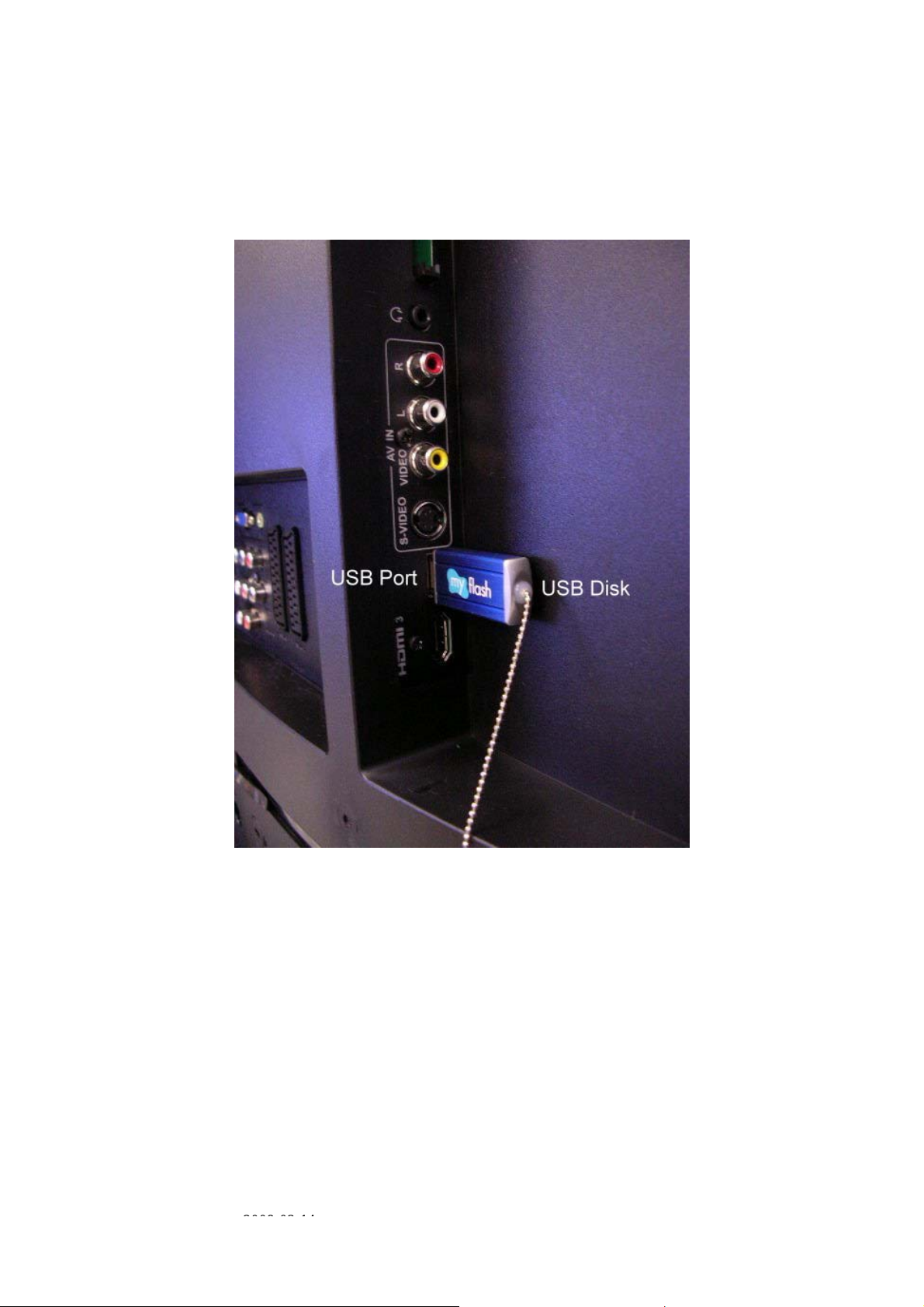
1.2 Connect to TV USB port to upgrade the software firmware
Please follow the following step to upgrade the firmware.
1. Copy the software firmware (*.pkg) to USB Disk.
2. Modify the pkg’s filename to “upgrade.pkg”
3. Insert the USB Disk to TV USB port.
LC-32SH25E
4. TV AC power off -> AC power on
5. TV will upgrade by itself after detect the USB disk condition and the content of the pkg file.
Note: TV’s Green LED will flash during upgrade process
6. After finish upgrade process, TV will reboot by itself.
7. Remove USB disk from TV.
8. Check the software version is correct or not.
(Menu / setup / Current software info)
2008-03-14
25
Page 26
LC-32SH25E
A
p
f
A
CHAPTER 4. TROUBLESHOOTING TABLE
[1] TROUBLESHOOTING TABLE
Power unit operation check.
↓
re the power cord and harness in the unit properly connected?
LINE_FILTER_UNIT: ↓ YES
Is F901 normal?
POWER_UNIT
Is BD901 (+320V) output? (Set the main power SW to OFF.)
* When power on/off switch is on ‧‧‧ About +400V
↓YES
↓YES
Is a voltage of +5V applied to pin (11,12) of connector (CN902)?
(Set the main power SW to OFF.)
↓YES
re +24V output as for the power on/off switch when it is on?
↓YES
Similarly, is +12V output as for the power on/off switch when it is
on?
NO
NO
NO
NO
NO
NO
Connect the power cord and harness properl y, and turn on the
ower.
LINE_FILTER_UNIT:
Isn't L901,L902,RV901,C903,C904,C901,C902, etc. out o
order? Moreover, whether the short-circuit with the
circumference circuit is checked.
POWER_UNIT:
BD901, RV902, IC951, etc. out of order?
Moreover, whether the short-circuit with the circumference circuit
is checked.
Does the PFC circuit operate normally?
(L906, Q901, D902, D903, IC901 and etc. And, the circuit around
the protection circuit etc. is checked.)
Does the switching circuit operate normally?
Check circuit around the primary side (T901, IC931, Q931,
ZD981, ZD930, D980, D981, ZD981, etc.), t he secondary side
(D935, L980, etc.), the AC_DET circuit (ZD982, IC932, IC982,
Q992, Q993, etc.), and the protection circuit.
Does the inverter circuit operate normally?
Check circuit around the primary side (T902,Q951,Q952,IC951,
D951,D952, etc.), the secondary side (D955, L971, ZD967,
IC952, IC953, etc.), the STANDBY circuit (Q988, etc.), and the
protection circuit.
Check +12V circuit of D956, L931, etc.
26
Page 27
The sound is not emitted from the speaker though the picture has come out.
↓
No sound output in all modes?
TEREMINAL UNIT: ↓
Is the audio signal output of pin (H26) (AL0) and pin (H25) (AR0) of
IC U400 normal?
NO
↓YES
Is the audio signal output of pin (17) (PGA2OUTL) and pin (18)
(PGA2OUTR) of IC U605 normal?
NO
↓YES
Is audio signal input to pin (2)(L), pin (14)(R) of IC U600 (AMP)?
NO
↓YES
Is MUTE circuit [AMP_MUTE_LINE, POWERUP_LINE] normal?
NO
↓YES
Is the audio signal output of pin (3, 4) (L-ch) and pin (1, 2) (R-ch) of
CN600 (AOUDIO-CONNECTOR) normal?
NO
↓YES
Check Speaker Box (right and left) and wire harness.
No sound (during the reception of TV(ANALOG) broadcasting)
↓
Does not the sound go out though the picture has come out when UHF/VHF is received?
TEREMINAL UNIT: ↓
Is the SIF signal output from pin (11) of TUNER (TU200)?
NO
↓YES
Is the SIF signal sent to pin (AB25) and pin (AB26) of IC U400?
NO
↓YES
Refer to “No sound output in all modes”.
2008-03-14
27
LC-32SH25E
Check IC U400 and its peripheral circuits.
Check IC U605 and its peripheral circuits.
Check the line between IC U605 and IC U600.
Check the AMP_MUTE_LINE and POWERUP_LINE. (Q600,
etc.)
Check IC U600 and its peripheral circuits.
Check the tuner and its peripheral circuits. Replace as required.
Check IC U400 its peripheral circuits.
Page 28
LC-32SH25E
f
f
No sound (during the reception of TV (DIGITAL) broadcasting)
↓
Does not the sound go out though the picture has come out when DTV is received?
MAIN UNIT: ↓
Is the DIF signal output from pin (17) and pin (19) of TUNER
(TU200)?
NO
↓YES
Is the DIF signal sent to pin (R25) and pin (T25) of IC U400?
NO
↓YES
Refer to “No sound output in all modes”.
No sound from external input devices (1)
↓
Does not the sound of the audio signal input to SCART1 go out?
Does not the sound of the audio signal input to SCART2 go out?
TEREMINAL UNIT: ↓
Is the audio signal properly sent to pin (6) (SCT1_AUL_IN) and pin
(2) (SCT1_AUR_IN) of SCART1(CN500)?
Is the audio signal properly sent to pin (6) (SCT2_AUL_IN) and pin
(2) (SCT2_AUR_IN) of SCART2(CN501)?
NO
NO
↓YES
Is the audio signal properly sent to pin (44) (SC1_LIN) and pin ( 43)
(SC1_RIN) of IC U605?
Is the audio signal properly sent to pin (46) (SC2_LIN) and pin ( 45)
(SC2_RIN) of IC U605?
NO
NO
↓YES
Refer to “No sound output in all modes”.
No sound from external input devices (2)
↓
Does not the sound of the audio signal input to AV1(Component) go out?
MAIN UNIT: ↓
Is the audio signal properly sent to pin (2) (AV1_AudioLIN) and pin
(4)(AV1_AudioRIN) of CN553?
NO
↓YES
Is the audio signal properly sent to pin (50) (AV1_LIN) and pin (49)
(AV1_RIN) of IC U605?
NO
↓YES
Refer to “No sound output in all modes”.
Check the tuner and its peripheral circuits. Replace as required.
Check IC U400 its peripheral circuits.
Check the setting of an external input device that connects o
CN500.
Check the setting of an external input device that connects o
CN501.
Check the line between CN500 and IC U605.
Check the line between CN501 and IC U605.
Check the connection to CN553 and the external input device.
Check the line between CN553 and IC U605.
28
Page 29
(
No sound from external input devices (3)
↓
Does not the sound of the audio signal input to AV3(Composite/Y/C) go out?
MAIN UNIT: ↓
Is the audio signal properly sent to pin (4) (AV3_AudioLIN) and pin
(6) (AV3_AudioRIN) of CN650?
↓YES
Is the audio signal properly sent to pin (52) (SIDE_LIN) and pin (51)
(SIDE_RIN) of IC U605?
↓YES
Refer to “No sound output in all modes”.
No sound from external input devices (4)
↓
Does not the sound of the audio signal input to VGA go out?
MAIN UNIT: ↓
Is the audio signal properly sent to pin (2) (VGA_AudioLI N) and pin
(3) (VGA_AudioRIN) of CN555?
↓YES
Is the audio signal properly sent to pin (48) (VGA_LIN) an d pin (47)
VGA_RIN) of IC U605?
↓YES
Refer to “No sound output in all modes”.
No sound from external input devices (5)
↓
Does not the sound of the audio signal input to HDMI1/2/3 go out?
↓
Is picture of the signal input from HDMI1/2/3 displayed?
↓YES
Refer to “No sound output in all modes”.
NO
NO
NO
NO
NO
LC-32SH25E
Check the connection to CN650 and the external input device.
Check the line between CN650 and IC U605.
Check the connection to CN555 and the external input device.
Check the line between CN555 and IC U605.
Refer to “Does not the picture of the HDMI signal input to
HDMI1/2/3 go out?”.
2008-03-14
29
Page 30
LC-32SH25E
The audio signal is not output (1)
↓
The audio signal of UHF/VHF is not output from SCART1.
TEREMINAL UNIT: ↓
Is audio signal output from IC U602 sent to pin (3)(SCT1_AULOUT) and pin(1)(SCT1_AUR-OUT) of SCART1(CN500)?
↓NO
Is audio signal output from IC U400 sent to pin (2)(LRCLK) and pin
(3)(DIN) and pin (4)(BCLK) and pin(13)(MCLK) of IC U602?
↓NO
Check IC U400 and its peripheral circuits.
The audio signal is not output (2)
↓
The audio signal of UHF/VHF/MONITOR is not output from SCART2.
TEREMINAL UNIT: ↓
Is audio signal output from IC U605 sent to
pin(3)(SCT2_AUL_OUT) and pin(1)(SCT2_AUR_OUT) of
↓NO
Is the audio signal output from IC U400 pin(K26) (AL2) and pin(J24)
(AR2) sent to pin(26)(INPUT1L) and pin(25)(INPUT1R) of IC U605?
↓NO
Check IC U400 and its peripheral circuits.
The audio signal is not output (3)
↓
No audio signal output from LINE_AUDIO_OUTPUT terminal.
TEREMINAL UNIT: ↓
Is audio signal output from IC U605 sent to pin(2)(L_OUT) and pin
(4)(R_OUT) of LINE_AUDIO_OUT connector(CN556)?
↓NO
Is the audio signal output from IC U400 pin(K26) (AL2) and pin(J24)
(AR2) sent to pin(26)(INPUT1L) and pin(25)(INPUT1R) of IC U605?
↓NO
Check IC U400 and its peripheral circuits.
YES
YES
YES
YES
YES
YES
Check the connection to SCART1 and external devices.
Check the line between IC U400 and IC U602.
Check the connection to SCART2 and external devices.
Check the line between IC U400 and IC U605.
Check the connection to LINE_AUDIO_OUT and external
devices.
Check the line between IC U400 and IC U605.
30
Page 31

f
The audio signal is not output (4)
↓
No audio signal output from SPDIF_OUTPUT terminal.
TEREMINAL UNIT: ↓
Is ASPDIF audio signal output from pin (E26) of IC U400 to pin (6)
of connector CN553?
↓NO
Check IC U400 and its peripheral circuits.
The audio signal is not output (5)
↓
No sound from HEADPHONE_OUTPUT terminal.
MINI AV_UNIT: ↓
Is the HPDET signal input into pin (AA5) of IC U400 from pin (7) o
a headphone terminal (CN602)?
↓YES
Is the audio signal output from IC U605 to pin(2) (HPOU TL) a nd pi n
(3) (HPOUTR) of headphone terminal CN602?
↓YES
Is the audio signal output from IC U400 pin(J26)(AL1) and pin(J25)
(AR1) sent to pin(24)(INPUT0L) and pin(23)(INPUT0R) of IC U605?
↓YES
Check IC U400 and its peripheral circuits.
YES
NO
NO
NO
LC-32SH25E
Check the connection to SPDIF_OUT and external devices.
Check the connection to CN602 and external headphone is plug
in well.
Check the line between IC U605 and CN602.
Check the line between IC U400 and IC U605.
2008-03-14
31
Page 32

LC-32SH25E
No picture on the display (1)
↓
The picture doesn't appear in all modes.
MAIN UNIT: ↓
Is LVDS signal output from 1st_channel and 2nd_channel of IC U400 in each mode?
(A0N/A0P),(A1N/A1P),(A2N/A2P),(A3N/A3P),(CLK1N/CLK1P)
↓NO
YES
Is the above-mentioned LVDS signals output to connector CN750?
NO
↓YES
Is LCD controller's control signal normal?
NO
PANEL_UNIT:
Similarly, is the LVDS signal input to connector of the panel
↓YES
NO
↓YES
Check the panel module.
No picture on the display (2)
↓
Does not the picture come out when VHF/UHF is received?
TERMINAL UNIT: ↓
Is TUNER_CVBS signal output from pin (21) of TUNER (TU200)?
NO
MAIN_UNIT: ↓YES
Is picture signal input from pin (21) of TUNER (TU200) to pin
(AB24) of IC U400?
NO
↓YES
Refer to “The picture doesn't appear in all modes.”
Check IC U400 and its peripheral control circuits.
Check the line between IC U400 and CN750.
Control signals BRIGHT_ADJ, INVERTER_ON_OFF,
PANEL_VCC_ON/OFF, and it peels off and whether normality is
checked.
Wire harness is checked.
Check whether I2C is normally accessed between TU200 and IC
U400.
Check the line between IC U400 and TU200.
32
Page 33

No picture on the display (3)
↓
Does not the picture come out when DTV is received?
TERMINAL UNIT: ↓
Is the voltage of regulation for a TUNER circuit and the power
supply terminal of IC U400 supplied?
↓YES
Is IF signal output from pin (17), (19) of TUNER (TU200) to pin
(R25), pin (T25) of IC U400 ?
↓YES
Is MPEG data (TS0INDATA0, TS0INSYNC, TS0INCLK,
TS0INVALID) from IC U400 are output to pin (9), pin (7), pin (6), pin
(8) of a IC U401?
MAIN_UNIT: ↓YES
Do X300 (60.00MHz)/ X400 (27MHz) oscillate?
↓YES
Is MPEG data (TS_DATAO, TS_CKO, TS_VALIDO, TS_SYNCO)
from IC U401 are output to pin (B21/A21/B20/C21) of a IC U400?
↓YES
Refer to “The picture doesn't appear in all modes.”
LC-32SH25E
NO
NO
NO
NO
NO
Each power supply circuit is checked.
Check the tuner, IC U400 and their peripher al circuits. Replace
as required.
is communication control carried out between pin (6)(SCL),
pin(9)(SDA), of TU200, and pin(F24)(TUNER_SCL1), pin
(F25)(TUNER_SDA1), of IC U400?
Check X300/ X400 and its peripheral circuits.
Is the control signal between IC U401 and IC U400 normal?
(RESET_CI, etc.).
2008-03-14
33
Page 34

LC-32SH25E
f
f
f
<External input SCART1, SCART2>No picture on the display (4)
↓
Does not the picture of the CVBS signal input to SCART1 go out?
Does not the picture of the CVBS signal input to SCART2 go out?
TERMINAL UNIT: ↓
Is CVBS signal sent to pin (20) of SCART1 (CN500)?
Is CVBS signal sent to pin (20) of SCART2 (CN501)?
MAIN_UNIT:
Is CVBS signal sent to pin (AE24) of IC U400?
Is CVBS signal sent to pin (AE26) of IC U400?
Refer to “The picture doesn't appear in all modes.”
↓YES
↓YES
<External input SCART1>No pict u re on the di sp lay (5)
↓
Does not the picture of the R/G/B video signal input to SCART1 go out?
TERMINAL UNIT: ↓
Is RGB signal sent to pin (15)/R, (11)/G, (7)/B, of SCART1
(CN500)?
MAIN_UNIT: ↓YES
Is RGB signal sent to pin (AF24)/R, (AD24)/G, (AD23)/B of IC
U400?
Refer to “The picture doesn't appear in all modes.”
↓YES
NO
NO
NO
NO
NO
NO
Check the setting of an external input device that connects o
CN500.
Check the setting of an external input device that connects o
CN501.
Check the line between IC U400 and CN500.
Check the line between IC U400 and CN501.
Check the setting of an external input device that connects o
CN500.
Check the line between IC U400 and CN500.
34
Page 35

f
f
f
f
<External input SCART1, SCART2>No picture on the display (6)
↓
Does not the picture of the Y/C signal input to SCART1 go out?
Does not the picture of the Y/C signal input to SCART2 go out?
TERMINAL UNIT: ↓
Is Y/C signal sent to pin (20) and (15) of SCART1 (CN500)?
Is Y/C signal sent to pin (20) and (15) of SCART2 (CN501)?
MAIN_UNIT:
Is Y/C signal sent to pin (AE24)/Y, (AF25)/C of IC U400?
Is Y/C signal sent to pin (AE26)/Y, (AE25)/C of IC U400?
Refer to “The picture doesn't appear in all modes.”
↓YES
↓YES
<External input AV3(Composite)>No picture on the display (7)
NO
NO
NO
NO
↓
Does not the picture of the composite video signal input to AV3(Composite) go out?
TERMINAL UNIT: ↓
Is CVBS signal sent to pin (2) of AV3 (CN650) ?
NO
MAIN_UNIT: ↓YES
Is CVBS signal sent to pin (AC24) of IC U400?
Refer to “The picture doesn't appear in all modes.”
↓YES
<External input AV3(Y/C)>No picture on the display (8)
NO
↓
Does not the picture of the Y/C video signal input to AV3(Y/C) go out?
TERMINAL UNIT: ↓
Is Y/C signal sent to pin (8)/Y, (7)/C of AV3 (CN650) ?
NO
MAIN_UNIT: ↓YES
Is Y/C signal sent to pin (AD26)/Y, (AD25)/C of IC U400?
Refer to “The picture doesn't appear in all modes.”
↓YES
NO
LC-32SH25E
Check the setting of an external input device that connects o
CN500.
Check the setting of an external input device that connects o
CN501.
Check the line between IC U400 and CN500.
Check the line between IC U400 and CN501.
Check the setting of an external input device that connects o
CN650.
Check the line between IC U400 and CN650.
Check the setting of an external input device that connects o
CN650.
Check the line between IC U400 and CN650.
2008-03-14
35
Page 36

LC-32SH25E
A
, (
A
A
<External input HDMI1>No picture on the display (9)
↓
Does not the picture of the HDMI signal input to HDMI1 go out?
MINI AV_UNIT: ↓
Is the HOT_PLUG detection function of pin (19) of a HDMI terminal
(CN702) normal?
YES
re EDID data pin (6)(SCL) of IC U708 (EEPROM), pin (5)(SDA)
accessed, and is it read from pin (15), pin (16) of a HDMI
terminal(CN702)?
Is TMDS signal input into pin (AF10, AE10)/RX2±, (AF9, AE9)/RX1
AF8, AE8)/RX0±, (AF7, AE7)/RXC± of IC U400?
±
Refer to “The picture doesn't appear in all modes.”
YES
↓YES
<External input HDMI2>No picture on the display (10)
↓
Does not the picture of the HDMI signal input to HDMI2 go out?
MINI AV_UNIT: ↓
Is the HOT_PLUG detection function of pin (19) of a HDMI terminal
(CN700) normal?
YES
re EDID data pin (6)(SCL) of IC U701 (EEPROM), pin (5)(SDA)
accessed, and is it read from pin (15), (16) of a HDMI
terminal(CN700)?
Is TMDS signal input into pin(AF14, AE14)/RX2±, (AF13,
E13)/RX1±, (AF12, AE12)/RX0±, (AF11, AE11)/RXC± of IC U400?
Refer to “The picture doesn't appear in all modes.”
YES
↓YES
NO
NO
NO
NO
NO
NO
Check the line between pin (AC4) of IC U400 and CN702.
↓
Check the connection and setup with the external HDMI devices.
Is access possible in the re-writing or exchange of EDID data of
IC U708?
↓NO
Check CN702, IC U708 and peripheral circuits.
Check the line between IC U400 and CN702.
Check the line between pin (AA6) of IC U400 and CN700.
↓
Check the connection and setup with the external HDMI devices.
Is access possible in the re-writing or exchange of EDID data of
IC U701?
↓NO
Check CN700, IC U701 and peripheral circuits.
Check the line between IC U400 and CN700.
36
Page 37

A
A
f
f
f
A
f
<External input HDMI3>No picture on the display (11)
↓
Does not the picture of the HDMI signal input to HDMI3 go out?
MINI AV_UNIT: ↓
Is the HOT_PLUG detection function of pin (19) of a HDMI terminal
(CN701) normal?
NO
Check the line between pin (AB5) of IC U400 and CN701.
Check the connection and setup with the external HDMI devices.
YES
re EDID data pin (6)(SCL) of IC U700 (EEPROM), pin (5)(SDA)
accessed, and is it read from pin (15), (16) of a HDMI
terminal(CN701)?
Is TMDS signal input into pin (AF18, AE18)/RX2±, (AF17,
E17)/RX1±, (AF16, AE16)/RX0±, (AF15, AE15)/RXC± of IC U400?
Refer to “The picture doesn't appear in all modes.”
YES
↓YES
<External input VGA>No picture on the display (12)
NO
NO
Is access possible in the re-writing or exchange of EDID data of
IC U700?
Check CN701, IC U700 and peripheral circuits.
Check the line between IC U400 and CN701.
↓
Does not the picture of the PC IN(ANALOG) video signal input to VGA(15pin-D-SUB terminal) go out?
TERMINAL_UNIT: ↓
Is R/G/B/H/V signal sent to pin (1)/R, (2)/G, (3)/B, (14 )/H, (13)/V o
VGA (CN554)?
MAIN_UNIT: ↓YES
Is R/G/B/H/V signal sent to pin (AE20)/R, (AE19)/G, (AD19)/B,
(AC18)/H, (AB18)/V of IC U400?
Refer to “The picture doesn't appear in all modes.”
↓YES
<External input AV1(Component)>No picture on the display (13)
NO
NO
Check the setting of an external input device that connects o
CN554.
Check the line between IC U400 and CN554.
↓
Does not the picture of the component video signal input to Component go out?
TERMINAL_UNIT: ↓
Is Component Y/Pb/Pr signal sent to pin (2)/Y, (4)/Pb, (6)/Pr o
V1(CN552) ?
MAIN_UNIT: ↓YES
Is Component Y/Pb/Pr signal sent to pin (AE21)/Y, (AD22)/Pb,
(AF22)/Pr of IC U400?
Refer to “The picture doesn't appear in all modes.”
↓YES
NO
NO
Check the setting of an external input device that connects o
CN552.
Check the line between IC U400 and CN552.
LC-32SH25E
↓
↓NO
2008-03-14
37
Page 38

LC-32SH25E
f
p
)
f
p
)
< During external connec t ion > No pi ctu r e o n the mo ni to r (1)
↓
No picture appears on SCART1 - connected monitor during the tuner (U/V) reception.
↓
Checklist:
1) Is the Signal Type (item) in MENU-Option-Input Select equal to Signal Type of an external device? …Set it to “CVBS”, “Y/C”, “RGB”, “AUTO”.
2) Is ANT-CABLE disconnected or connected improperly? …Connect it correctly as per the operation manual.
3) The picture is sent to the monitor in a CVBS signal if the source during display is ATV, CVBS or Y/C of SCART1-2, AV3.
When sent by component, etc., that signal is not sent to the monitor.
4) When the monitor picture is not sent and is not displayed on the monitor, refer to “No picture” for each terminal.
5) The video output from SCART1 is not the monitor output (output of the picture now watching).
The
icture of the last selected TV channel is always sent to SCART1. (Specification
TERMINAL_UNIT:
Is CVBS signal output into pin (19) of CN500 (SCART1)?
↓NO
Is TUNER_CVBS signal output into pin (21) of CN500 (SCART1)?
Refer to “The picture doesn't appear in all modes.”
↓
↓NO
YES
YES
Check the setting of an external input device that connects o
CN500.
Check the line between CN500 and TU200.
< During external connec t ion > No pi ctu r e o n the mo ni to r (2)
SCART2: ↓
No picture from SCART1 appears on SCART2-connected monitor.
NOTE: Normally, if the screen during display is sent to SCART2, no picture is sent to SCART2.
↓
Checklist:
1) Is the Signal Type (item) in MENU-Option-Input Select equal to Signal Type of an external device? …Set it to “CVBS”, “Y/C”, “AUTO”.
2) The picture is sent to the monitor in a CVBS signal if the source during display is TV, CVBS or Y/C of SCART1-2, AV3.
When sent by component, etc., that signal is not sent to the monitor.
3) When the monitor picture is not sent and is not displayed on the monitor, refer to “No picture” for each terminal.
4) The video output from SCART1 is not the monitor output (output of the picture now watching).
The
TERMINAL_UNIT:
Is CVBS signal output into pin (19) of CN501 (SCART2)?
↓NO
Is CVBS signal output from pin (A13) of IC U400 into pin (19) of
CN501 (SCART2)?
Refer to “The picture doesn't appear in all modes.”
icture of the last selected TV channel is always sent to SCART1. (Specification
↓
YES
YES
↓NO
Check the setting of an external input device that connects o
CN501.
Check the line between CN501 and IC U400.
38
Page 39

LC-32SH25E
CHAPTER 5. MAJOR IC INFORMATIONS
[1] MAJOR IC INFORMATIONS
1. MAJOR IC INFORMATIONS
1.1. U400 (MT5362CHG/A)
GENERAL DESCRIPTION
The MediaTek MT5362CHG/A family consists of a DTV(DVB-T) front-end demodulator, a backend decoder and a TV controller and offers high
integration for advanced applications. It combines a transport de-multiplexer, a high definition video decoder, an AC3 audio decoder, an dual-link LVDS
transmitter, and an NTSC/PAL/SECAM TV decoder with a 3D comb filter(NTSC/PAL). The MT5362CHG/A enables consumer electronics manufactures to
build high quality, low cost and feature-rich DTV.
World-Leading Audio/Video Technology: The MT5362CHG/A supports most Full-HD video decoder standards including H.264, MPEG4, MPEG2 and
JPEG. The MT5362CHG/A also supports MediaTek MDDi
to the TV decoder recovers great details for still pictures. The special color processing technology provides natural, deep colors and true studio quality
video. Also, the MT5362CHG/A family has built-in high resolution and high-quality audio codec.
Rich Features for High Value Products: The MT5362CHG/A family enables true single-chip experience. It integrates high-quality HDMI1.3, high speed
VGA ADC, dual-channel LVDS, USB2.0 receiver and multi-media decoder
Reliable DVB-T Receiving capability: MT5362CHG/A family supports DVB-T demodulation function. Excellent adjacent and co-channel rejection
capability grants customers never miss any wonderful stream. Professional error-concealment provides stable, smooth and mosaic-free video quality.
Key Features:
1. DVB-T demodulator
2. A transport demultiplexer
3. A multi-standard video decoder
4. An AC3/MPEG2 audio decoder
5. HDMI1.3 receiver
6. Audio codec
Note: All packages are lead free
General Feature List
□ Host CPU
· ARM 926EJS
· 16K I-Cache and 16K D-Cache
· 8K Instruction TCM
· JTAG ICE interface
· Watch Dog timers
· Build-in CPI analyzer and Cache Hit Rate Meter
□ Transport Demultiplexer
· Supports a serial or parallel transport stream input
· Supports ATSC, DVB, MPEG-2 transport stream input
· Supports DES/3-DES/DVB/AES de-scramblers
· Up to 8-PID even/odd keys for descrambling
· Support 32 PID filters and 32 section filters
· Support micro-processor section filtering
· Support hardware CRC-32 check
· Support PCR recovery function
· Support a micro-processor for stream process and MPEG start code detection
· Support DVB CA
· Support simple trick play (Playback / Pause /Fast Forward (upto x32)) through USB or Flash
□ MPEG2 Decoder
· MPEG MP@ML, MP@HL and MPEG-1 video standards
· Support de-blocking filter
□ MPEG1 Decoder
□ MPEG4.2 Decoder
· ASP@15 (720P)
□ H.264 (MPEG4.10) HD Decoder (AVC)
· MP@L4.1, HP@L4.1, BP@L3 (baseline) video standard
□ Still Image decoding
· JPEG (base-line or progressive)
□ De-mosquito engine
· 2D/3D for all AV inputs
□ 2D Graphics
· Support multiple color modes
· Point, horizontal/vertical line primitive drawings
2008-03-14
TM
de-interlace solution to reach very smooth picture quality for motions. A 3D comb filter added
39
Page 40

LC-32SH25E
· Rectangle fill and gradient fill functions
· Bitblt with transparent options
· Alpha blending and alpha composition Bitblt
· Stretch Bitblt
· Font rendering by color expansion
· YCbCr to RGB color space conversion
□ Image Resizer
· Support 2/4/8bpp index format, 16bpp/32bpp direct color format.
· Support 420/422 video format.
· Support 420/422/444 JPEG format.
· Arbitrary ratio vertical/horizontal scaling of video, from 1/128X to 128X
· Simple DMA.
□ OSD Plane
·Two linking list OSDs with multiple color mode and one of them has scaler
□ Video Plane
· Support video capture and over scan.
· Flesh tone management
· Gamma correction
· Color Transient Improvement (CTI)
· 2D Peaking
· Saturation/hue adjustment
· Brightness and contrast adjustment
· Black and White level extender
· Adaptive Luma/Chroma management
· Automatic detect film or video source
· 3:2/2:2 pull down source detection
· Support maximum 1920 width motion-adaptive de-interlace.
· Support excellent low angle image processing.
· Arbitrary ratio vertical/horizontal scaling of video, from 1/32X to 32X
· Advanced non-linear panorama scaling.
· Programmable zoom viewer
· Progressive scan output
· Support alpha blending
· Dithering processing for flat panel display
· Frame rate conversion.
· Support FHD panel and VGA dot-to-dot
· Support PIP/POP, (dual de-interlace, one HD and one SD)
□ LVDS
· Support 6/8/10-bit one – channel or 6/8-bit dual-channel LVDS transmitter, 2-link LVDS up-to 175 MHz
· Built-in spread spectrum for EMI performance
· Programmable panel timing output
□ CVBS In
· On-chip 54 MHz 10-bit video ADC
· Support PAL (B,G,D,H,M,N,I,Nc), NTSC,
· NTSC-4.43, SECAM
· Macrovision detection
· NTSC/PAL support 3D/2D comb filter
· Built-in motion-adaptive 3D Noise Reduction
· VBI data slicer for CC/TT decoding
· Support 2-S-Video.
· Max. Support 4-channel CVBS.
· Support SCART connector
□ VGA In
· Support VGA input up to UXGA 162 MHz
· Support full VESA standards
□ Component Video In
· Support two component video inputs
· Support 480i / 480p / 576i / 576p / 720p / 1080i / 1080p
□ Audio ADC
· 2 channel on chip Audio ADC
□ Audio digital input
· 1 bit I2S audio input
□ HDMI Receiver
· HDMI1.3, data rate can be up to 2.25 GHz
· EIA/CEA-861B
· CEC
40
Page 41

LC-32SH25E
□ Video bypass (for EU application)
· TVbypass
· CVBS Monitor (any AV input)
□ TV audio demodulator
· Support BTSC / EIA-J / A2 / NICAM / PAL FM /
· SECAM world-wide formats
· Standard automatic detection
· Stereo demodulation, SAP demodulation
· Mode selection (Main/SAP/Stereo)
□ Audio DAC
· 6 on-chip audio DACs (3-pair) support R/L channel and subwoofer outputs
□ DRAM Controller
· 32-bit DDR1/2 interface
· Support 8MB to 128 MB DDR DRAM devices
· Support DDR1-400, DDR1-500, DDR2-667 DDR2-800
□ Audio DSP
· Support Dolby Digital AC-3 decoding (ATSC)
· MPEG-1 layer I/II decoding (DVB)
· Dolby Prologic II
· Support WMA / HE-AAC / DTS / ADPCM /
· LPCM
· Audio output: 7.1ch + 2ch (down mix)
· Pink noise and white noise generator
· Equalizer
· Bass management
· 3D surround processing with virtual surround
· Audio and video lip synchronization
· Support reverberation
· Automatic volume control
· Support 5-bit (10-channel) main audio I
· Support 1-bit (2-channel) aux audio I
□ S/PDIF interface
· One SPDIF input
· One SPDIF out
□ Digital TV(DVB-T) Demodulator
· COFDM(Coded Orthogonal Frequency Division Multiplex) channel demodulator for DVB-T receiver
· ETSI 300 744 & Nordig Unified compliant
· Excellent performance for SFN(Single Frequency Network) & Indoor reception
· Support 2K, 8K modes
· Support QPSK,16,64 QAM constellations
· 1/4,1/8,1/16,1/32 Guard interval
· Support hierarchical & non-hierarchical modes
· Accept 6,7,8 MHz channel bandwidth
· Automatic mode detection
· Full-digital timing/frequency with wide acquisition range
· Support triple offset
· Excellent adjacent Channel interference (ACI) rejection capability
· Excellent Co-Channel interference(CCI) rejection capability
· Fast channel lock time
□ Analog TV IF Demodulator
· Support PAL/SECAM standard
· Accept IF frequency at 38.25 MHz
· Full digital AGC control and carrier recovery
□ Peripherals
· Each of the MT5362CHG/A has one built-in UART with Tx and Rx FIFO. It has hardware flow control and high speed data transferring.
· The MT5362CHG/A family has three basic serial interfaces; one is for the tuner, one is the master for general purpose, the other is the slave for
HDMI EDID data.
· Three PWMs
· While NAND Flash is disabled, the MT5362CHG/A support MS/MS-PRO, SD/MMC, and SDHC card reader.
· IR blaster and receiver
· Real-time clock and watchdog controller
· The MT5362CHG/A includes 2-link USB2.0/1.1 (support external hub) for USB mass storage class device.
· Built-in uP in standby module
· SDIO interface (for DSG, WiFi or UWB)
· Support two serial flash or one serial and one NAND
· Support five-input low-speed ADC.
2008-03-14
2
S output interface: each of these channels is up to 24-bit resolution.
2
S output I/F: each of these channels is up to 24-bit resolution.
41
Page 42

LC-32SH25E
· Support boundary scan (JTAG)
□ IC Outline
· MT5362CHG/A is 27x27 mm BGA Package
· 3.3V/1.0V and 1.8V for DDR2
1.2. U103, U104 (L5985 VFQFPN8)
Description
The L5985 is a step down switching regulator with 2.5A current limited embedded power MOSFET, so it is able to deliver up to 2A DC current to the load
depending on the application condition.
The input voltage can range from 2.9V to 18V, while the output voltage can be set starting from 0.6V to V
. Having a minimum input voltage of 2.9V, the
IN
device is suitable for buses staring from for 3.3V bus.
Requiring a minimum set of external components, the device includes an internal 250KHz switching frequency oscillator that can be externally adjusted up
to 1MHz.
The QFN package with exposed pad allows reducing the R
down to approximately 60°C/W.
thJA
Features
· 2A DC output current
· 2.9V to 18V input voltage
· Output voltage adjustable from 0.6V
· 250KHz switching frequency, programmable up to 1MHz
·Internal Soft-start and Inhibit
· Low dropout operation: 100% duty cycle
· Voltage feed-forward
· Zero load current operation
· Over current and thermal protection
· VQFN3x3-8L package
Applications
· Consumer:
STB, DVD, DVD recorder, car audio, LCD TV and monitors
· Industrial:
Chargers, car battery, PLD, PLA, FPGA
· Networking: XDSL, modems, DC-DC modules
· Computer:
Optical storage, hard disk drive, printers, audio/graphic cards
1.3. U351, U352 (HYB18TC512160B2F-25 TFBGA84)
Features
The 512-Mbit Double-Data-Rate-Two SDRAM offers the following key features:
· 1.8 V ± 0.1 V Power Supply
· 1.8 V ± 0.1 V (SSTL_18) compatible I/O
· DRAM organizations with 8, 16 data in/outputs
· Double Data Rate architecture:
- two data transfers per clock cycle
- four internal banks for concurrent operation
· Programmable CAS Latency: 3, 4, 5 and 6
· Programmable Burst Length: 4 and 8
· Differential clock inputs (CK and CK)
· Bi-directional, differential data strobes (DQS and DQS) are transmitted / received with data. Edge aligned with read data and center-aligned with write
data.
· DLL aligns DQ and DQS transitions with clock
· DQS can be disabled for single-ended data strobe operation
· Commands entered on each positive clock edge, data and data mask are referenced to both edges of DQS
· Data masks (DM) for write data
· Posted CAS by programmable additive latency for better command and data bus efficiency
· Off-Chip-Driver impedance adjustment (OCD) and On-Die-Termination (ODT) for better signal quality.
· Auto-Precharge operation for read and write bursts
· Auto-Refresh, Self-Refresh and power saving Power-Down modes
· Average Refresh Period 7.8 µs at a T
lower than 85 °C, 3.9 µs between 85 °C and 95 °C
CASE
· Programmable self refresh rate via EMRS2 setting
· Programmable partial array refresh via EMRS2 settings
· DCC enabling via EMRS2 setting
· Full and reduced Strength Data-Output Drivers
· 1K page size for x8, 2KB page size for x16
· Packages: PG-TFBGA-84, PG-TFBGA-60
· RoHS Compliant Products
1
)
· All Speed grades faster than DDR2-400 comply with DDR2-400 timing specifications when run at a clock rate of 200 MHz.
42
Page 43

LC-32SH25E
1.4. U600 (TDA8933BTW HTSSOP32)
General description
The TDA8933B is a high-efficiency class D amplifier with low power dissipation.
The continuous-time output power is 2 × 10 W in a stereo half-bridge application (R
to the low power dissipation the device can be used without any external heat sink when playing music. Due to the implementation of thermal foldback(TF)
the device remains operating with considerable music output power without the need for an external heat sink, even for high supply voltages and/or lower
load impedances.
The device has two full differential inputs driving two independent outputs. It can be used in a mono full-bridge configuration (Bridge-Tied Load(BTL)) or as
stereo half-bridge configuration (Single-Ended(SE)).
Features
· Operating voltage from 10 V to 36 V asymmetrical or ±5 V to ±18 V symmetrical
· Mono bridge-tied load (full-bridge) or stereo single-ended (half-bridge) application
· Application without heat sink using thermally enhanced small-outline package
· High efficiency and low-power dissipation
· Thermal foldback to avoid audio holes
· Current limiting to avoid audio holes
· Full short-circuit proof across load and to supply lines (using advanced current protection)
· Switchable internal or external oscillator (master-slave setting)
· No pop noise
· Full differential inputs
Applications
· Flat-panel television sets
· Flat-panel monitor sets
· Multimedia systems
· Wireless speakers
· Mini/micro systems
· Home sound sets
= 8 Ω) or 1 × 20 W in a mono full-bridge application (RL =16 Ω). Due
L
1.5. U602 (WM8521H9GED/RV SOIC-14)
DESCRIPTION
The WM8521 is a 96kHz stereo DAC with an integrated output op-amp stage, designed to generate a 2.0Vrms output signal directly, so reducing external
component requirements in digital audio applications.
WM8521 comes into two variants WM8521HC and WM8521H9 which offers different line drive output capabilities. WM8521HC outputs 2Vrms at 12V
supply, while WM8521H9 outputs 2.0Vrms at 9V supply. WM8521HC/H9 are designed for cost sensitive consumer digital audio applications requiring
2Vrms line output.
A 24-bit multi-bit sigma delta DAC is used with oversampling digital interpolation filters. Digital audio input word lengths from 16-32 bits and sampling rates
from 8kHz to 96kHz are supported.
The audio interface supports I
The devices are controlled via a hardware interface which provides access to features including de-emphasis, mute and data formats. These devices are
pin equivalent and are available in a 14-pin SOIC package.
FEATURES
· Audio Performance
- DAC SNR 98dB (‘A’ weighted @ 48kHz)
- THD -81dB (‘A’ weighted @ 48kHz)
· DAC Sampling Frequency: 8kHz – 96kHz
· Pin Selectable Audio Data Interface Format
2
S, 16-bit Right Justified or 16bit DSP
- I
· 2.0 Vrms output at 12V or 9V supply
· 8.2V to 13.2V Analogue, 2.7V to 3.6 Digital Supply
· 14-pin SOIC Package
APPLICATIONS
· Consumer digital audio applications requiring 2 Vrms output
- DVD Players
- Digital TV
- Digital Set Top Boxes
- A/V Receivers
2
S, Right Justified and DSP digital audio formats.
2008-03-14
1.6. U401 (MT8295AE LQFP-128)
43
Page 44

LC-32SH25E
FEATURES
■ PCMCIA/CI Interface
· Single slot PC Card interface
· Single slot CI interface
· 512 byte embedded buffer
■ Host Interface
· NAND flash interface
· Interrupt capability
· 3.3V logic levels
■ Transport Stream Interface
· MPEG2 compliant TS
· One parallel or two serial TS interface from demodulator
· Serial TS interface to MPEG2 decoder
· Parallel TS interface from/to CAM
· Supports serial to parallel TS conversion
· Supports parallel to serial TS conversion
■ Miscellaneous
· 27 MHz crystal
· 60 MHz clock input
· Integrated PLL
· 3.3/1.8V process
· 5V compatible I/Os for PC Card interface
· Supports additional 15 GPIOs
· LQFP 128-pin package
1.7. U390 (MX25L3205DMI-12G SOP-16)
FEATURES
GENERAL
· Serial Peripheral Interface compatible -- Mode 0 and Mode 3
· 32M:33,554,432 x 1 bit structure or 16,772,216 x 2 bits (two I/O read mode) structure
· 1024 Equal Sectors with 4K byte each (32Mb)
- Any Sector can be erased individually
· 64 Equal Blocks with 64K byte each (32Mb)
- Any Block can be erased individually
· Single Power Supply Operation
- 2.7 to 3.6 volt for read, erase, and program operations
· Latch-up protected to 100mA from -1V to Vcc +1V
· Low Vcc write inhibit is from 1.5V to 2.5V
PERFORMANCE
• High Performance
- Fast access time: 86MHz serial clock (15pF + 1TTL Load) and 66MHz serial clock (30pF + 1TTL Load)
- Serial clock of two I/O read mode : 50MHz (15pF + TTL Load), which is equivalent to 100MHz
- Fast program time: 1.4ms(typ.) and 5ms(max.)/page (256-byte per page)
- Byte program time: 7us (typical)
- Continuously program mode (automatically increase address under word program mode)
- Fast erase time: 60ms(typ.) /sector (4K-byte per sector) ; 0.7s(typ.) /block (64K-byte per block); 25s(typ.) for 32Mb
· Low Power Consumption
- Low active read current: 25mA(max.) at 86MHz, 20mA(max.) at 66MHz and 10mA(max.) at 33MHz
- Low active programming current: 20mA (max.)
- Low active erase current: 20mA (max.)
- Low standby current: 20uA (max.)
- Deep power-down mode 1uA (typical)
· Typical 100,000 erase/program cycles
SOFTWARE FEATURES
· Input Data Format
- 1-byte Command code
· Advanced Security Features
- Block lock protection
The BP0-BP3 status bit defines the size of the area to be software protection against program and erase instructions
- Additional 512-bit secured OTP for unique identifier
· Auto Erase and Auto Program Algorithm
- Automatically erases and verifies data at selected sector
- Automatically programs and verifies data at selected page by an internal algorithm that automatically times the program pulse widths (Any page to be
44
Page 45

programed should have page in the erased state first)
· Status Register Feature
· Electronic Identification
- JEDEC 1-byte manufacturer ID and 2-byte device ID
- RES command for 1-byte Device ID
- Both REMS and REMS2 commands for 1-byte manufacturer ID and 1-byte device ID
HARDWARE FEATURES
· SCLK Input
- Serial clock input
· SI Input
- Serial Data Input
· SO Output
- Serial Data Output
· WP#/ACC pin
- Hardware write protection and program/erase acceleration
· HOLD# pin
- pause the chip without diselecting the chip
· PACKAGE
- 16-pin SOP (300mil)
- 8-land WSON (8x6mm or6x5mm)
- 8-pin SOP (200mil, 150mil)
- 8-pin PDIP (300mil)
- All Pb-free devices are RoHS Compliant
1.8. U155 (IC TPS5430DDAR SO-8(DDA))
FEATURES
· Wide Input Voltage Range:
– TPS5430: 5.5 V to 36 V
– TPS5431: 5.5 V to 23 V
· Up to 3-A Continuous (4-A Peak) Output Current
· High Efficiency up to 95% Enabled by 110-m
· Wide Output Voltage Range: Adjustable Down to 1.22 V with 1.5% Initial Accuracy
· Internal Compensation Minimizes External Parts Count
· Fixed 500 kHz Switching Frequency for Small Filter Size
· Improved Line Regulation and Transient Response by Input Voltage Feed Forward
· System Protected by Over Current Limiting and Thermal Shutdown
· –40°C to 125°C Operating Junction Temperature Range
· Available in Small Thermally Enhanced 8-Pin SOIC PowerPAD™ Package
· For SWIFT Documentation, Application Notes and Design Software, See the TI Website at www.ti.com/swift
Ω Integrated MOSFET Switch
LC-32SH25E
DESCRIPTION
As a member of the SWIFT™ family of DC/DC regulators, the TPS5430/TPS5431 is a high-output-current PWM converter that integrates a low resistance
high side N-channel MOSFET. Included on the substrate with the listed features are a high performance voltage error amplifier that provides tight voltage
regulation accuracy under transient conditions; an undervoltage-lockout circuit to prevent start-up until the input voltage reaches 5.5 V; an internally set
slow-start circuit to limit inrush currents; and a voltage feed-forward circuit to improve the transient response. Using the ENA pin, shutdown supply current
is reduced to 18 mA typically. Other features include an active-high enable, over-current protection, and thermal shutdown. To reduce design complexity
and external component count, the TPS5430/TPS5431 feedback loop is internally compensated. The TPS5431 is intended to operate from power rails up
to 23 V. The TPS5430 regulates a wide variety of power sources including 24-V bus.
The TPS5430/TPS5431 device is available in a thermally enhanced, easy to use 8-pin SOIC PowerPAD™ package. TI provides evaluation modules and
the SWIFT™ Designer software tool to aid in quickly achieving high-performance power supply designs to meet aggressive equipment development cycles.
1.9. U605 (IC MT8292 QFN-48)
2008-03-14
45
Page 46

LC-32SH25E
46
Page 47

2. Detailed ICs Information
_
_
_
_
2.1. U400 (MT5362CHG/A)
2.1.1 Block Diagram
2.1.2 Pin Connections and short description
LC-32SH25E
RA4
RA
VDAC_O
GPIO1
UT2
12
AVDD
A
VSS
LV
DS
1
VCCK
VCCK VCCK
LVDS
VCCK
A
AVDD12
VSS12
VPLL VPLL
2008-03-14
47
Page 48

LC-32SH25E
_
DVSS
VCCK VCCK
2.2. U103, U104 (L5985 VFQFPN8)
2.2.1 Pin Connections and short description
Type Description
N°
OUT Regulator output
1
SYNCH Master/Slave Synchronization. When it is left floating, a signal with a phase shift of half a period respect to the power turn
2
INH A logical signal (active high) disable the device. With INH higher than 1.9V the device is OFF and with INH lower than
3
COMP Error Amplifier output to be used for loop frequency compensation
4
FB Feedback input. Connecting the output voltage directly to this pin the output voltage is regulated at 0.6V. To have higher
5
The switching frequency can be increased connecting an external resistor from FSW pin and ground. If this pin is left
F
6
SW
GND Ground
7
V
8
Unregulated DC input voltage
CC
2.3. U351, U352 (HYB18TC512160B2F-25 TFBGA84)
2.3.1 Pin Connections and short description
AVDD12_R
GB_DIG
on is present at the pin. When connected to an external signal at a frequency higher than the internal one, then the
device is synchronized by the external signal, with zero phase shift.
Connecting together the SYNC pin of two devices, the one with higher frequency works as master and the other one as
slave; so the two power turn on have a phase shift of half a period.
0.6V the device is ON.
regulated voltages an external resistor divider is required from Vout to FB pin.
floating the deice works at its free-running frequency of 250KHz.
AVSS12
P
LL LL
AVSS12_P
LL
AVSS12_P
LL
LL
48
AOSDATA
2
AOSDATA3AOSDATA0AOSDATA
AOSDATA
4
AOLRCK AOMCLK ALIN
IF_AGC RF_AGC ASPDIF
TN ER_CLU
K ATA
AVICM
CVBS0P
AOBCK
NER_DU
T
VM D
VIP_ATV
CVBS0N
1
I
VINDC
Page 49

Ball# Name Ball Type Buffer Type Function
Clock Signals ×16 Organization
J8 CK I SSTL
K8 CK I SSTL
K2 CKE I SSTL Clock Enable
Control Signals ×16 Organization
K7 RAS I
L7 CAS I
K3 WE I
L8 CS I
Address Signals ×16 Organization
L2 BA0 I
L3 BA1
M8 A0
M3 A1
M7 A2
N2 A3
N8 A4
N3 A5
N7 A6
P2 A7
P8 A8
P3 A9
M2
P7 A11
R2 A12
Data Signals ×16 Organization
G8
G2
H7
H3
H1 DQ4 I/O SSTL
H9 DQ5 I/O SSTL
F1 DQ6 I/O SSTL
F9 DQ7 I/O SSTL
C8 DQ8 I/O SSTL
C2 DQ9 I/O SSTL
D7 DQ10 I/O SSTL
D3 DQ11 I/O SSTL
D1 DQ12 I/O SSTL
D9 DQ13 I/O SSTL
B1 DQ14 I/O SSTL
B9 DQ15 I/O SSTL
A10
AP
DQ0 I/O SSTL
DQ1 I/O SSTL
DQ2 I/O SSTL
DQ3 I/O SSTL
2008-03-14
I
SSTL
I
SSTL
I
SSTL
I
SSTL
I
SSTL
I
SSTL
I SSTL
I SSTL
I SSTL
I SSTL
I
SSTL
I
SSTL
I
SSTL
I
SSTL
I
SSTL
SSTL
SSTL
SSTL
SSTL
SSTL
Clock Signal CK, CK
Row Address Strobe (RAS),
Column Address Strobe(CAS),
Write Enable(WE)
Chip Select
Bank Address Bus 1:0
Address Signal 12:0, Address
Signal 10/Autoprecharge
Data Signal Lower Byte 7:0
Data Signal Upper Byte 15:8
49
LC-32SH25E
Page 50

LC-32SH25E
Data Strobe ×16 Organization
B7 UDQS
A8 UDQS
F7
E8
LDQS
LDQS
I/O SSTL
I/O SSTL
I/O SSTL
I/O SSTL
Data Strobe Upper Byte
Data Strobe Lower Byte
Data Mask ×16 Organization
B3 UDM
F3
LDM
I SSTL
I SSTL
Data Mask Upper Byte
Data Mask Lower Byte
Power Supplies ×16 Organization
J2 V
A9, C1, C3, C7, C9, E9,
AI — I/O Reference Voltage
REF
V
PWR
DDQ
—
I/O Driver Power Supply
G1, G3, G7, G9
J1 V
A1, E1, J9, M9, R1 VDD
A7, B2, B8, D2, D8, E7,
PWR
DDL
PWR —
V
SSQ
PWR —
—
Power Supply
Power Supply
I/O Driver Power Supply
F2, F8, H2, H8
J7 V
A3, E3,J3,N1,P9 VSS
SSDL
PWR —
PWR —
Power Supply
Power Supply
Not Connected ×16 Organization
A2, E2, L1, R3, R7, R8 NC
NC
— Not Connected
Other Pins ×16 Organization
K9 ODT I SSTL On-Die Termination Control
2.4. U600 (TDA8933BTW HTSSOP32)
2.4.1 Block Diagram
2.4.2 Pin Connections and short description
/N2
50
Page 51

Symbol Pin Description
VSSD(HW)
IN1P
IN1N
DIAG
ENGAGE
POWERUP
CGND
VDDA
VSSA
OSCREF
HVPREF
INREF
TEST
IN2N
IN2P
VSSD(HW)
VSSD(HW)
DREF
HVP2
VDDP2
BOOT2
OUT2
VSSP2
STAB2
STAB1
VSSP1
OUT1
BOOT1
VDDP1
HVP1
OSCIO
VSSD(HW)
1
2
3
4
5
6
7
8
9
10
11
12
13
14
15
16
17
18
19
20
21
22
23
24
25
26
27
28
29
30
31
32
negative digital supply voltage and handle wafer connection
positive audio input for channel 1
negative audio input for channel 1
diagnostic output; open-drain
engage input to switch between Mute mode and Operating mode
power-up input to switch between Sleep mode and Mute mode
control ground; reference for POWERUP, ENGAGE and DIAG
positive analog supply voltage
negative analog supply voltage
input internal oscillator setting (only master setting)
decoupling of internal half supply voltage reference
decoupling for input reference voltage
test signal input; for testing purpose only
negative audio input for channel 2
positive audio input for channel 2
negative digital supply voltage and handle wafer connection
negative digital supply voltage and handle wafer connection
decoupling of internal (reference) 5 V regulator for logic supply
half supply output voltage 2 for charging single-ended capacitor for channel 2
positive power supply voltage for channel 2
bootstrap high-side driver channel 2
Pulse Width Modulated (PWM) output channel 2
negative power supply voltage for channel 2
decoupling of internal 11 V regulator for channel 2 drivers
decoupling of internal 11 V regulator for channel 1 drivers
negative power supply voltage for channel 1
PWM output channel 1
bootstrap capacitor for channel 1
positive power supply voltage for channel 1
half supply output voltage 1 for charging single-ended capacitor for channel 1
oscillator input in slave configuration or oscillator output in master configuration
negative digital supply voltage and handle wafer connection
2.5. U602 (WM8521H9GED/RV SOIC-14)
2.5.1 Block Diagram
2008-03-14
LC-32SH25E
51
Page 52

LC-32SH25E
BCLK
LRCLK
DIN
2.5.2 Pin Connections and short description
DIN
1
2
3
4
5
6
7
DGND
LRCLK
BCLK
MUTE
VOUTR
AGND
PIN NAME TYPE DESCRIPTION
1 DGND Supply Digital Negative supply
2 LRCLK Digital input Sample rate clock input
3 DIN Digital input Serial audio data input
4 BCLK Digital input Bit clock input
5 MUTE Digital input
6 VOUTR Analogue output Right channel DAC output
7 AGND Supply Analogue Negative supply
8 CAP Analogue output Analogue internal reference
9 AVDD Supply Analogue Positive supply
10 VOUTL Analogue output Left channel DAC output
11 DEEMPH Digital input
12 FORMAT Digital input
13 MCLK Digital input Master clock input
14 DVDD Supply Digital Positive supply
2.6. U401 (MT8295AE LQFP-128)
2.6.1 Block Diagram
FORMAT MUTE DEEMPH
DIGITAL AUDIO
INTERFACE
&
DI GITA L FILT ER S
DVDD
14
MCLK
13
FORMAT
12
DEEMPH
11
VOUTL
10
AVD D
9
CAP
8
CONTROL
INTERFACE
SIGMA
DELTA
MODULATOR
SIGMA
DELTA
MODULATOR
DVDD DGND AVDD AGND
Soft mute control, Internal pull down
High Impedance = Automute
High = Mute ON
Low = Mute OFF
De-emphasis select, Internal pull down
High = de-emphasis ON
Low = de-emphasis OFF
Data input format select, Internal pull up
Low = 16-bit right justified or 16bit DSP ‘late’
High = 16-32-bit I
2
S or 16bit DSP ‘early’
RIGHT
DAC
LEFT
DAC
VOUTR
VOUTL
CAP
52
Page 53

2.6.2 Pin Connections and short description
Pin Number
M0 M1 M2
Miscellaneous
107 RESETB I N/A Chip reset
114 100 117 CI_INT O 4~16mA Interrupt 1
NAND flash
116 102 115 CI_DATA0 I/O 4~16mA NAND Flash Data bit 0 1
115 101 114 CI_DATA1 I/O 4~16mA NAND Flash Data bit 1 1
95 96 106 CI_DATA2 I/O 4~16mA NAND Flash Data bit 2 1
102 117 105 CI_DATA3 I/O 4~16mA NAND Flash Data bit 3 1
101 116 103 CI_DATA4 I/O 4~16mA NAND Flash Data bit 4 1
100 115 102 CI_DATA5 I/O 4~16mA NAND Flash Data bit 5 1
99 95 101 CI_DATA6 I/O 4~16mA NAND Flash Data bit 6 1
98 94 100 CI_DATA7 I/O 4~16mA NAND Flash Data bit 7 1
94 99 116 CI_CEB I N/A NAND Flash Chip enable 1
106 98 99 CI_RB O 4~16mA NAND Flash Ready 1
96 114 94 CI_WEB I N/A NAND Flash Write enable 1
103 105 95 CI_ALE I N/A NAND Flash Address Latch enable 1
105 103 96 CI_CLE I N/A NAND Flash Command Latch enable 1
117 106 98 CI_OEB I N/A NAND Flash Output enable 1
CLK/Crystal
109 XTALO O N/A Crystal output
110 XTALI I N/A Crystal input
Transport stream (TS)
6 T0CLK I N/A Transport stream 1 input clock
7 T0SYNC I N/A Transport stream 1 input sync.
8 T0VALID I N/A Transport stream 1 input valid
9 T0DATA0 I N/A Transport stream 1 input data bit 0
11 T0DATA1 I N/A
12 T0DATA2 I N/A
13 T0DATA3 I N/A
14 T0DATA4 I N/A
16 T0DATA5 I N/A Transport stream 1 input data bit 5
17 T0DATA6 I N/A Transport stream 1 input data bit 6
18 T0DATA7 I N/A Transport stream 1 input data bit 7
123 TS_CKO O 4~16mA Transport stream output clock
125 TS_SYNCO O 4~16mA Transport stream output sync.
122 TS_VALIDO O 4~16mA Transport stream output valid
124 TS_DATAO O 4~16mA Transport stream output data
General Purpose Input and Output (GPIO)
1 GPIO0 I/O 4~16mA General purpose I/O bit 0
2 GPIO1 I/O 4~16mA General purpose I/O bit 1
Symbol Type Driving Description Note
Transport stream 1 input data bit 1
Transport stream 2 input clock
Transport stream 1 input data bit 2
Transport stream 2 input sync
Transport stream 1 input data bit 3
Transport stream 2 input valid
Transport stream 1 input data bit 4
Transport stream 2 input data
2
2
2
2
2008-03-14
53
LC-32SH25E
Page 54

LC-32SH25E
3 GPIO2 I/O 4~16mA General purpose I/O bit 2
4 GPIO3 I/O 4~16mA General purpose I/O bit 3
19 GPIO4 I/O 4~16mA General purpose I/O bit 4
20 GPIO5 I/O 4~16mA General purpose I/O bit 5
21 GPIO6 I/O 4~16mA General purpose I/O bit 6
91 GPIO7 I/O 4~16mA General purpose I/O bit 7
92 GPIO8 I/O 4~16mA General purpose I/O bit 8
93 GPIO9 I/O 4~16mA General purpose I/O bit 9
118 GPIO10 I/O 4~16mA General purpose I/O bit 10
119 GPIO11 I/O 4~16mA General purpose I/O bit 11
120 GPIO12 I/O 4~16mA General purpose I/O bit 12
127 GPIO13 I/O 4~16mA General purpose I/O bit 13
128 GPIO14 I/O 4~16mA General purpose I/O bit 14
PCMCIA/CI
83 D0 I/O 4~16mA PCMCIA data bit 0
85 D1 I/O 4~16mA PCMCIA data bit 1
87 D2 I/O 4~16mA PCMCIA data bit 2
24 D3 I/O 4~16mA PCMCIA data bit 3
26 D4 I/O 4~16mA PCMCIA data bit 4
28 D5 I/O 4~16mA PCMCIA data bit 5
30 D6 I/O 4~16mA PCMCIA data bit 6
32 D7 I/O 4~16mA PCMCIA data bit 7
81 D8 I/O 4~16mA PCMCIA data bit 8
84 D9 I/O 4~16mA PCMCIA data bit 9
86 D10 I/O 4~16mA PCMCIA data bit 10
25 D11 I/O 4~16mA PCMCIA data bit 11
27 D12 I/O 4~16mA PCMCIA data bit 12
29 D13 I/O 4~16mA PCMCIA data bit 13
31 D14 I/O 4~16mA PCMCIA data bit 14
34 D15 I/O 4~16mA PCMCIA data bit 15
80 A0 O 4~16mA PCMCIA address bit 0
78 A1 O 4~16mA PCMCIA address bit 0
75 A2 O 4~16mA PCMCIA address bit 0
73 A3 O 4~16mA PCMCIA address bit 0
71 A4 O 4~16mA PCMCIA address bit 0
69 A5 O 4~16mA PCMCIA address bit 0
66 A6 O 4~16mA PCMCIA address bit 0
64 A7 O 4~16mA PCMCIA address bit 0
46 A8 O 4~16mA PCMCIA address bit 0
44 A9 O 4~16mA PCMCIA address bit 0
37 A10 O 4~16mA PCMCIA address bit 0
41 A11 O 4~16mA PCMCIA address bit 0
62 A12 O 4~16mA PCMCIA address bit 0
48 A13 O 4~16mA PCMCIA address bit 0
50 A14 O 4~16mA PCMCIA address bit 0
59 A15 O 4~16mA PCMCIA address bit 0
57 A16 O 4~16mA PCMCIA address bit 0
45 A17 O 4~16mA PCMCIA address bit 0
47 A18 O 4~16mA PCMCIA address bit 0
49 A19 O 4~16mA PCMCIA address bit 0
51 A20 O 4~16mA PCMCIA address bit 0
54 A21 O 4~16mA PCMCIA address bit 0
56 A22 O 4~16mA PCMCIA address bit 0
58 A23 O 4~16mA PCMCIA address bit 0
61 A24 O 4~16mA PCMCIA address bit 0
63 A25 O 4~16mA PCMCIA address bit 0
67 RESET O 4~16mA PCMCIA reset
35 CE1_ O 4~16mA PCMCIA card enable 1
36 CE2_ O 4~16mA PCMCIA card enable 2
23 CD1_ I N/A PCMCIA card detection 1
88 CD2_ I N/A PCMCIA card detection 2
38 VS1_ I N/A PCMCIA voltage sense 1
65 VS2_ I N/A PCMCIA voltage sense 2
79 BVD1 I N/A PCMCIA battery voltage detection 1
77 BVD2 I N/A PCMCIA battery voltage detection 2
72 INPACK_ I N/A PCMCIA input port acknowledge
70 WAIT_ I N/A PCMCIA wait
54
Page 55

40 IORD_ O 4~16mA PCMCIA IO read strobe
42 IOWR_ O 4~16mA PCMCIA IO write strobe
74 REG_ O 4~16mA PCMCIA register selection
79 OE_ O 4~16mA PCMCIA output enable
53 WE_ O 4~16mA PCMCIA write enable
55 READY I N/A PCMCIA ready
89 WP I N/A PCMCIA write protect
Power & Ground
5 VCC33 I N/A I/O power 3.3V
33 VCC33 I N/A I/O power 3.3V
52 VCC33 I N/A I/O power 3.3V
68 VCC33 I N/A I/O power 3.3V
97 VCC33 I N/A I/O power 3.3V
121 VCC33 I N/A I/O power 3.3V
10 GND33 I N/A Ground
43 GND33 I N/A Ground
60 GND33 I N/A Ground
76 GND33 I N/A Ground
104 GND33 I N/A Ground
126 GND33 I N/A Ground
15 VCC18 I N/A Core power 1.8V
82 VCC18 I N/A Core power 1.8V
22 GND18 I N/A Ground
90 GND18 I N/A Ground
108 AVDD33_XTAL I N/A Analog crystal power 3.3V
111 AVSS33_XTAL I N/A Analog crystal ground
112 AVDD18_PLL I N/A Analog PLL power 1.8V
113 AVSS18_PLL I N/A Analog PLL ground
2.7. U390 (MX25L3205DMI-12G SOP-16)
2.7.1 Block Diagram
SI/SIO0
SO/SIO1
WP#/ACC,
CS#,
HOLD#
SCLK
Address
Generator
Data
er
Regist
Mode
Logic
Clock Generator
SRAM
Buffer
2.7.2 Pin Connections and short description
HOLD#
SO/SIO1
VCC
CS#
NC
NC
NC
NC
1
2
3
4
5
6
7
8
SCLK
16
SI/SIO0
15
NC
14
NC
13
NC
12
NC
11
GND
10
2008-03-14
WP#/ACC
9
State
Machine
Memory Array
Page Bu
ff e r
Y-Decoder
HV
Generator
Sense
Amplifier
Output
Buffer
LC-32SH25E
55
Page 56

LC-32SH25E
2.8. U155 (IC TPS5430DDAR SO-8(DDA))
2.8.1 Block Diagram
2.8.2 Pin Connections and short description
2.9. U605 (IC MT8292 QFN-48)
2.9.1 Block Diagram
56
Page 57

2.9.2 Pin Connections and short description
LC-32SH25E
2008-03-14
57
Page 58

LC-32SH25E
58
Page 59

CHAPTER 6. BLOCK DIAGRAM/WIRING DIAGRAM
[1] VIDEO & AUDIO BLOCK DIAGRAM
LC-32SH25E
59
Page 60

LC-32SH25E
[2] POWER MANAGEMENT BLOCK DIAGRAM
60
Page 61

[3] I2C and RS232 BLOCK DIAGRAM
LC-32SH25E
2008-03-14
61
Page 62

LC-32SH25E
[4] WIRING DIAGRAM
62
Page 63

CHAPTER 7. PRINTED WIRING BOARD
[1] MAIN UNIT PRINTED WIRING BOARD
MAIN UNIT(Side-A)
LC-32SH25E
2008-03-14
63
Page 64

LC-32SH25E
MAIN UNIT(Side-B)
64
Page 65

[2] POWER UNIT PRINTED WIRING BOARD
POWER UNIT(Side-A)
LC-32SH25E
2008-03-14
65
Page 66

LC-32SH25E
POWER UNIT(Side-B)
66
Page 67

[3] KEY UNIT PRINTED WIRING BOARD
KEY UNIT (Side-A) KEY UNIT (Side-B)
LC-32SH25E
2008-03-14
67
Page 68

LC-32SH25E
[4] IR UNIT PRINTED WIRING BOARD
IR UNIT (Side-A) IR UNIT (Side-B)
68
Page 69

CHAPTER 8. SCHEMATIC DIAGRAM
[1] MAIN SCHEMATIC DIAGRAM
01. POWER-1
EU SHARP MT5362 - 4 LAYERS
BRIGHT_ADJ:
Normal:M ax:+ 3V3, M i n:0V
DC POWER INPUT
3
6
5
0
2
1
4
0
0
0
0
0
0
0
1
1
1
1
1
1
1
P
P
P
P
P
P
P
CN100
CONN
T
T
1
1
1
2
3
4
5
6
7
8
9
10
11
12
LOCK TYPE
T
T
T
T
T
1
1
1
1
1
Stand_By:0V
INVERTER_ON_OFF:
Normal: High
Stand_B y: Low
INVERTER_ON_OFF
BRIGHT_ADJ
+12V
+24V
STB_PWR5V
STANDBY:
Normal: High
Stand_by: Low
SMD/0402
R113 100R 1/16W 5%
SMD/0402
R142 NC/ 100R 1/ 16W 5%
STANDBY
OPWRSB
1K 1/16W 5%
SMD/0402
STANDBY
R144
Q106
BC847C
STB_PWR5V
DV33SBDV33
R129
NC/ 2K2 1/ 16W 5%
SMD/0402
R108
NC/0R05 1/16W
FB100 220R/2000mA
1 2
FB101 220R/2000mA
1 2
SMD/0402
C124
100N 16V
SMD/0402
R126
1K 1/16W 5%
SMD/0402
+5V_STB
C106
+
C107
100N 16V
4
7
0
u
F
1
6
V
+5V_STB +5V_TunerB+
+5V_SW +5V1_TUN
STAND_BY
STAND_BY:
Normal: Low
Stand_by: High
R149
0R05 1/4W
R105
NC/ 0R 05 1/ 4W
IF 5V HAVE DIP
IF 5V NO DIP
R143
NC/ 0R 05 1/ 4W
R150
0R05 1/4W
+
C110
220uF 16V
OPWRSB (+5V_SW ON/OFF):
Normal: High
Stand_By: Low
OPWRSB
R147
%
5
W
0
1
/
1
K
1
/
C
N
+12V
+5V_SW
+5V_ STB (+5V1) TO +5V_SW BY OPWRS B
R107
1K 1/10W 5%
C135
LC-32SH25E
CN100 B1 C101 B8
+5V_STB +5V_SW
Q104 SI5441DC
1
8
D
D
2
9
1
1
R
W
0
1
/
1
K
2
2
2
C121
V
V
6
0
1
1
F
N
u
0
2
0
2
1
/
C
N
7
D
D
3
6
D
D
5
G4S
C105
100N 16V
R130
5K1 1/10W
3
Q101
BC847C
1
+
C101
100uF 16V
C114
4.7UF 10V
R111
+3V3SB DV33SB
0 OHM +-5% 1/8W
+24V2,13
+12V2,9,13
+5V_STB2,5,7
+5V_SW2,5,8,9,10,11,12,13,14
+5V1_TUN2
DV18_DDR6
DV114
OPWRSB5
STAND_BY5
BRIGHT_ADJ14
INVERTER_ON_OFF14
DV332,4,5,7,8,12, 13,14
+3V3SB2
DV33SB4,5,7,10,12,13,14
MEM_VREF6
GND2,3,4,5,6,7,8,9,10,11,12,13, 14
+24V
+12V
+5V_STB
+5V_SW
+5V1_TUN
DV18_DDR
DV11
OPWRSB
STAND_BY
BRIGHT_ADJ
INVERTER_ON_OFF
DV33
+3V3SB
DV33SB
MEM_VR EF
GND
C102 G2 C104 G4
C105 B8 C106 B5
C107 B5 C108 F3
C109 G4 C110 E5
C111 F6 C112 F1
C114 B8 C118 F9
C119 G9 C120 G9
C121 C7 C123 G10
C124 C4 C125 G3
C126 G7 C127 G8
C128 F4 C129 F2
C130 F5 C131 F1
C132 F4 C135 C7
D100 F5 D101 F2
FB100 A4 F B 101 B4
L101 F2 L102 F5
Q100 G7 Q101 B8
Q103 F7 Q104 B8
Q106 C4 Q108 G3
Q109 G3 R100 G7
R101 G7 R102 F7
R103 G7 R104 F2
R105 B5 R106 F4
R107 B7 R108 C4
R111 D9 R113 C2
R114 F9 R115 G1
R116 G5 R117 G1
R119 B8 R120 F7
R122 G5 R123 G5
R124 F1 R125 F5
R126 C4 R127 G3
R128 G4 R129 B4
R130 B8 R131 F8
R132 G9 R135 F3
R136 F3 R137 G1
R142 C2 R143 E6
R144 B4 R147 C6
R149 B5 R150 E6
TP100 B1 TP101 B1
TP102 B1 TP103 B1
TP104 B1 TP105 B1
TP106 B1 U102 F9
U103 F4 U104 F2
DV18_DDR
+
C112
330UF 16V
USE 330uF 16V GF
NC/ 1K 1/ 10W 5%
0.6 x (1+ 2.44K/1. 2K) = 1. 82V
R124
C131
NC/ 22N 16V
R137
W
0
1
/
1
%
1
+
M
H
O
K
2
.
2
2008-03-14
L10115uH
2
D101
W
SS3P4
0
1
/
1
%
1
1
-
+
M
H
O
0
4
2
R115
1%
R117
1.2KOHM +-1% 1/10W
1%
R104
33N 16V
OPWRSB(+1V8):
Normal: High
Stand_By: Low
OFF: Low
C102
C108
10U 16V
U104
L5985
1
2
V
0
5
P
0
3
3
C129
3
OPWRSB
W
0
1
/
1
%
5
+
M
H
O
K
9
.
3
Vout
SYNC
GND
INH
FSW
1
COMP4FB
H
T
9
10K 1/10W 5%
Vcc
R127
8
7
6
5
6
5
3
3
1
1
R
R
W
W
0
0
1
1
/
/
1
1
%
%
5
5
-
-
+
+
M
M
H
H
O
O
K
K
7
7
4
4
Q108
C
7
5
4
2
8
1
C
C
B
V
6
1
N
0
0
1
From +5V_SW to +1V8/+1V1 By OPWRSB
C
7
4
8
C
B
Q109
C132
10U 16V
9
0
1
C
V
6
1
N
0
0
1
U103
L5985
8
Vcc
7
GND
6
FSW
5
1
FB
H
T
9
R128
10K 1/10W 5%
Vout
SYNC
COMP
INH
1
2
3
4
OPWRSB
C128
V
0
5
P
0
3
3
L102 15uH
2
D100
W
SS3P4
0
1
/
1
%
5
1
+
M
H
O
R106
K
9
.
3
C104
33N 16V
OPWRSB(+1V1):
Normal: High
Stand_By: Low
OFF: Low
0.6 x (1+1.1K/1.2K) = 1. 15V
W
6
2
1
R125
0
/
4
1
C130
0
/
5
0
D
NC/22N 16V
R
M
0
S
W
0
1
/
1
R123
1%
%
1
+
M
H
O
K
1
.
1
R116
NC/ 1K 1/ 10W 5%
R122
1.2KOHM +-1% 1/10W
1%
DV11
+
C111
330UF 16V
USE 330uF 16V GF
R120 NC/0R 05 1/ 4W
1
6
D
D
2
5
D
D
4
G3S
Q103
SI3441BDV
R103
22K 1/10W
STANDBY
R100
22K 1/10W
STANDBY:
Normal : High
Stand_by: Low
R101
22K 1/10W
100N 16V
C126
3
2
1
+5V_STB TO +5V1_TUN
FOR IF HAVE 5V DIP
R102
5K1 1/10W
Q100
BC847C
+5V1_TUN+5V_TunerB+
C127
10U 10V Y5V
DV18_DDR
R131 1K 1/10W 1%
R132
1K 1/10W 1%
C118
NC/ 100N 16V
C119
1UF16V
VTT
R114 NC/4K7 1/10W
U102
1
GND
MEM_VREF
C120
100N 16V
SMD/0402
2
3
SD
PVIN
VSENSE
AVIN
VREF4VDDQ
S
H
9
VTT
NC/LP2996MRX
DV18_DDR stabilizer
8
7
6
5
C123
100N 16V
DV18_DDR
69
Page 70

LC-32SH25E
02. POWER-2
C166
100N 16V
Add Thermal Pad
+5V_SW
U151
LD1117ADT33TR
3
VIN
D
N
G
1
+5V_SW TO AV 33 +5V_STB TO +3V3SB(For CEC MCU)
+5V_SW
1
A
K
2
C160
100N 16V
SMD/0402
Vo= 1 . 25 x (1+ 120 R/ 120R) = 2.5V
Add Thermal Pad
D150
RGP15D
U153
LD1117ADT-TR
3
VIN
VOUT
D
J
N
D
A
G
/
1
C168
10U 10V
+5V_SW TO AV 25
Add Thermal Pad
+5V_SW DV33
U157
LD1117DT33TR
3
VIN
C158
100N 16V
+5V_SW TO DV33
AV33
2
VOUT
VOUT
J
D
A
/
+
C159
100uF 16V
2
R152
R151
2
+
J
D
A
/
120 OHM +-1% 1/10W
120 OHM +-1% 1/10W
D
N
G
1
AV25
C150
100uF 16V
C161
+
100UF 25V
KH SERIES
+5V_STB +3V3SB
U152
AME8810-AEGTZ 0.6A/3.3V
2
D
N
G
C155
10U 16V
+5V_TUNER+5V1_TUN
C151
100N 16V
3
VOUT(heat sink )
VIN
4
1
4
FB150 NC/220R/2000mA
1 2
R168 NC/1.5 OHM 1/4W
R156 NC/1.5 OHM 1/4W
+5V_T UNER FR OM +5V 1_T UN
Add Thermal Pad
U154
AV25 AV12
LD1117DTTR
C164
100N 16V
SMD/0402
3
VIN
C153
10U 10V
Vo=1.25 x (1+1R/120R) = 1.26V
2
VOUT
D
J
N
D
A
G
/
120 OHM +-1% 1/10W
1
1 OHM +-5% 1/10W
R162
R163
C162
+
100uF 16V
AV25 TO AV12
+12V
+24V
R177
NC/ 0R 05 1/ 4W
PANEL_VCC_ON/OFF
C172
+
4
7
0
u
F
3
5
V
R176
0R05 1/4W
C165
100N 50V
R154
100 OHM +-5% 1/10W
PANEL_VCC_ON/OFF:(GPIO5)
Normal:High
Stand_By:Low
Panel VCC=12V
PANEL_VCC ON/OFF:(GPIO5)
Normal:High
Stand_By:Low
PANEL_VCC_ON/OFF
Panel VCC=5V
5
6
7
8
NC/ 56R 1/ 8W
NC/ 330P 50V
R153
0R05 1/8W
R158 N C / 1K 1/ 10 W 5%
V
6
1
N
0
0
1
/
C
N
TPS5430DDAR
ENA
GND
VIN
PH
9
R160
C174
NC/ 0R 05 1/ 8W
C156
W
0
1
/
9
1
5
1
K
0
R
1
/
C
N
4
VSENSE
3
NC
2
d
NC
a
1
p
BOOT
-
G
U155
R169
NC/ 56R 1/ 8W
4.7KOHM +-1% 1/10W
R171
0R05 1/10W
1
5
2
1
D
1
1.22 x (1+15K/ 4. 7K) = 5.1V
PANEL_VCCPANEL5V
R155
Q150
8
D
7
D
6
D
5
NC/SI5441DC
R157
NC/ 2K2 1/ 10W 5%
R164
NC/ 1K 1/ 10W 5%
Q151
NC/BC847C
C163
10N 50V
4
P
3
S
S
R161
Use new comp
1
D
2
D
3
D
G4S
R166
15KOHM +-1% 1/10W
L150 22uH
PANEL_VCC+12V
C167
+
SMD
V
5
2
F
u
0
1
/
C
N
C157
NC/4.7uF25V
PANEL5V
+
C154
330UF 16V
+24V1,13
+12V1,9,13
+5V_STB1,5,7
+3V3SB1
+5V_SW1,5,8,9,10,11,12,13,14
+5V_TUNER3
+5V1_TUN1
DV331,4,5,7,8,12,13,14
AV333,5,10,11,12,13,14
DV33SB1,4,5,7,10,12,13,14
AV125,6,10,12,14
PANEL_VCC14
AV253
DV18_CI8
PANEL_VCC_ON/OFF5
GND1,3,4,5,6,7,8,9,10,11,12,13,14
Panel VCC deviation
ITEM
R164
Q151
R155
R157
Q150
R158
R159
C167
C156
C157
R171
C163
R153
R154 100R
R161
R166
C172
L150
C154
U155
C165
D151
R176
PANEL
VCC:+12V
1K N/C
BC847C
0R
2K2
SI5441
1K
10K
10U
100N
4U7
N/C
N/C 10N
N/C
N/C
N/C
N/C
N/C
N/C
N/C
N/C
N/C
N/C
N/C
PANEL
VCC: + 5 V
N/C
N/C
N/C
N/C
N/C
N/C
N/C
N/C
N/C
0R
0R
4K7
15K
470U
22U
330U
TPS543 0
100N
SS3P4
0R
+24V
+12V
+5V_STB
+3V3SB
+5V_SW
+5V_TUNER
+5V1_TUN
DV33
AV33
DV33SB
AV12
PANEL_VCC
AV25
DV18_CI
PANEL_VCC_ON/OFF
GND
C150 E2 C151 A3
C152 G8 C153 E3
C154 B8 C155 A4
C156 E6 C157 E8
C158 E1 C159 A2
C160 C1 C161 C2
C162 E4 C163 B7
C164 E3 C165 B6
C166 A1 C167 E8
C168 C1 C172 B 6
C173 G1 C174 C7
C175 G2 C176 G7
C177 G5 C178 G6
D150 B1 D151 B7
FB150 B3 L150 B8
Q150 D7 Q151 E7
R151 C2 R152 C2
R153 C6 R154 B 6
R155 D7 R156 C3
R157 E7 R158 E6
R159 E7 R160 B7
R161 B8 R162 E4
R163 E4 R164 E7
R166 A8 R168 C3
R169 B7 R171 B7
R172 G7 R173 G7
R174 G6 R175 F8
R176 A6 R177 A6
U151 A1 U152 A3
U153 C1 U154 D3
U155 A7 U157 E1
U158 G1 U159 F6
C173
100N 16V
SMD/0402
U158 LD1117S18
VI3VO
D
N
G
4
1
4
+5V1_TUN +5V_TUNER
+5V_ TUNER dev iat ion
of dif f er ent Power board
U159
2
VIN
1
C177
+
47uF 16V
SMD
DV18_CIDV33
2
C175
10U 10V
VINH
GND3ADJ
LD29150PTR
4
VO
W
C178
47uF 16V
SMD
W
0
0
1
1
/
/
1
1
%
%
1
1
3
-
2
-
7
+
7
+
1
1
M
M
R
R
H
H
O
O
K
K
0
1
5
2
5
+
W
0
1
/
1
%
1
4
-
7
+
1
M
R
H
O
K
7
.
4
+5V_TUNER FROM Regulator
C176
V
5
2
N
1
R175
0R05 1/4W
C152
+
470uF 16V
SMD
HV type
ITEM
FB150
R175
U159
R174
C178
R172
R173
C176
C177
POWER
32"/37"
N/C
0R
LD39080
4K7
47UF/16V
20K
51K
1N/25V
47UF/16V
POWER
42"/47"
BEAD
N/C
N/C
N/C
N/C
N/C
N/C
N/C
N/C
70
Page 71

03. TUNER
Panasonic
AVSS33_DIG
AVDD33_DIG
TUNER_CLK
RF_AGC
TUNER_DATA
VIN_ATV
VIP_ATV
DVSS25_IFADC
AVSS25_IFADC
AVSS25_IFADC
AVSS25_REF
DVDD25_IFADC
AVDD25_IFADC
AVDD25_REF
AVSS33_SIF
AVDD33_SIF
MT5362-PBGA470
Tuner
TU200
NXP
TU201
R205
100R
NC
R239
NC
0R
AS_TUNER
AS_IF
AS_TUNER
+5V_TUN
RF_AGC
NC/NXP FQD1116ME
U400B
IF_AGC
VINDC
SIFP
SIFN
TU201
TH4
TH3
CVBS
AS_IF
SIF2
SIF1
+5V IF
DIF2
DIF1
IF_AGC
SDA
SCL
GND
GND
GND
AntPwr
RF_IO
TH2
TH1
AF
NC
NC
NC
NC
VT
NC
R206
100R
NC
AA22
Y23
E24
F24
E25
F25
R25
T25
T26
V22
U23
T24
P25
V23
U24
P26
AA24
AB25
AB26
Y22
W22
28
27
24
23
22
21
20
19
18
17
16
15
14
13
12
11
10
9
8
7
6
5
4
3
2
1
26
25
AVSS33_DIG
AVDD33_DIG
IF_AGCT
TUN ER _SCL1
RF_AGC
TUNER_SDA1
FAT_INFAT_IN+
VINDC
DVSS25_IFADC
AVSS25_IFADC
AVSS25_IFADC
AVSS25_IFADC
DVDD25_IFADC
AVDD25_IFADC
AVDD25_IFADC
MPX0P
MPX0N
AVSS33_SIF
AVDD33_SIF
FB206
R222
NC
NC
BEAD
0R
R220
NC/ 0R 05 1/ 10W 5%
R221
NC/ 0R 05 1/ 10W 5%
R222
NC/ 0R 05 1/ 10W 5%
TUNER_CVBS
AS_IF
IF_AGC_OUT
SDA
SCL
AS_TUNER
TUNER_RFAGC
TP2001
C238
100N 16V
TUN ER _R FAGC
C226
NC
100N
+5V_T3
+5V_T4
10K 1/10W 5%
C227
NC
100N
+5V_T3
+5V_TUNER
R228
R237
NC/ 100KOHM +-5% 1/10W
NC/ 100KOHM +-5% 1/10W
R223
R224
NC
NC
330R
330R
C228
NXP_DIF1
NC/3.3pF
R223 NC / 330 OH M 1/16W
R224 NC / 330 OH M 1/16W
C247
47N 16V
IF_AGC
R238
C228
NC
3P3
NXP_DIF1
NXP_DIF2
NXP_DIF2
SMD/0402
SMD/0402
C206
100N 16V
AV25
C233
1uF/16V
RFAGC
R225
R226
NC
NC
100R
100R
SMD/0402
R225
NC/ 100R 1/ 16W 5%
R226
NC/ 100R 1/ 16W 5%
SMD/0402
NXP_MPX0
NXP_DIF1
1 2
FB206
NC/120R/500mA
C226
NC/ 100N 16V
+5V_T1
C205
10U 10V
FB208
1 2
120R/500mA
R218
R217
0R
0R
75R
75R 75R
R239
NC/ 100R 1/ 16W 5%
SMD/0402
NXP_MPX0NXP_DIF2
C227
NC/ 100N 16V
FB202
1 2
120R/500mA
R219
NC
DFAT_IN+
DFAT_IN-
MPX0
+5V_TUNER
C215
100N 16V
AVDD25_IFADC
TU200
C232
100N 16V
SMD/0402
VIDEO OUT
AFT OUT
IF T OU T 2
IFD OUT 1
AUDI O OU T
BT Monitor
AGC Monitor
+B active ANT
C234
4.7UF 10V
AVSS25_IFADC
Panasonic ENG37E14KF
+5V_T2
TH4
TH3
IF AGC
SIF OU T
SDA
SCL
TH2
TH1
LC-32SH25E
AVDD33_SIF
C214
4.7UF 10V
AVSS33_SIF
R209
4K7 1/10W
C225
100P 50V
+5V_TUNER+5V_T
C212
100N 16V
SMD/0402
TUNER_SDA1
TUNER_SCL1
2X CVBS LEVEL
AMPLIFIER
SCT1_TV_OUT
R236
NC/ 0R 05 1/ 10W 5%
+5V_MUX
SCART1 TV BYPASS
SMD/0402
C203 100N 16V
R211
10 OHM +-5% 1/10W
75R 1/10W 1%
R213
TUNER_CVBSN
Q200
2SD2653K
+
470uF 16V
HV type
AV332,5,10,11,12,13,14
+5V_TUNER2
AV252
+5V_MUX9
GND1,2,4,5,6,7,8,9,10,11,12,13,14
SCT1_TV_OUT9
ATV_CVBS_OUT9
RFAGC5
CVBS0P10
CVBS0N10
SCT1_AV_OUT9
SCT1_AVO_GND9
SCT1_TV_BYPASS
C222
75R 1/ 10W 1%
SMD
R204
0R05 1/10W 5%
100R 1/16W 5%
75R 1/16W 5%
R217
R215
SMD/0402
R227
AV33
+5V_TUNER
AV25
+5V_MUX
GND
SCT1_TV_OUT
ATV_CVBS_OUT
RFAGC
CVBS0P
CVBS0N
SCT1_AV_OUT
SCT1_AVO_GND
Tuner
Panasonic
TU200
TU201
-
2
-
>
<
-
-
|
>
1
Close to
MT5336
NXP
SCT1_AV_OUT
ZD200
UDZSNP5.6B
SCT1_AVO_GND
C210
47N 16V
SMD/0402
C221
1UF 6V3
SMD/0402
R218
R219
0R
NC
75R 75R
CVBS0P
CVBS0N
C200 E5 C201 A7
C202 A8 C203 F9
C204 B6 C205 A3
C206 A3 C207 D7
C208 D7 C209 G7
C210 G10 C211 G8
C212 B8 C213 B7
C214 B8 C215 A4
C216 A4 C217 A5
C218 A5 C219 A6
C220 A7 C221 H10
C222 F9 C223 D5
C224 C8 C22 5 C8
C226 F3 C227 F3
C228 E2 C229 B7
C230 B6 C231 B7
C232 B4 C233 B3
C234 B4 C235 B6
C236 B4 C237 B5
C238 B2 C239 E7
C244 E8 C245 C7
C246 C7 C247 A2
FB200 A 8 F B 2 01 A8
FB202 A 3 F B 2 03 A5
FB204 A 6 F B 2 05 A7
FB206 E 3 F B 2 07 A6
FB208 A 3 F B 2 09 A5
Q200 F9 Q201 G7
Q202 E7 Q203 E7
R200 D6 R20 1 D6
R202 B6 R203 F5
R204 F9 R205 C6
R206 C6 R20 7 C8
R208 H8 R20 9 C8
R210 F6 R211 F9
R212 E6 R213 F9
R214 G6 R215 G9
R216 G7 R217 F9
R218 G7 R219 G8
R220 D2 R221 E2
R222 E2 R223 E3
R224 E3 R225 D3
R226 D3 R22 7 H9
R228 A2 R229 C6
R230 C6 R231 E7
R232 F7 R233 F7
R234 F7 R235 E8
R236 E9 R237 B2
R238 B3 R239 E3
R240 F5 TP200 A2
TU200 B4 TU201 E1
U400B A1 ZD200
F10
FB209
1 2
120R/500mA
TUNER_CVBS
+5V_T1
+5V_T2
IF_AGC_OUT
SIF
SDA
SCL
+5V_T3
+5V_T4
DIF2
DIF1
+5V_T
C217
100N 16V
+5V_T3
DVDD25_IFADC
C237
4.7UF 10V
DVSS25_IFADC
MPX0
MPX0
C223
NC/ 15P 50V
1 2
C218
10U 10V
0R05 1/16W
0R05 1/16W
FB203
1 2
120R/500mA
C216
10U 10V
AV25
C236
1uF/16V
25
24
21
20
19
18
NC
17
16
VB
15
+B
14
NC
13
NC
12
11
10
9
8
NC
7
NC
6
5
BB
4
3
NC
2
1
23
22
TUNER_RFAGC
+5V_T +5V_T+5V_T
FB204
+5V_T4
120R/500mA
C235
100N 16V
SMD/0402
10N 50V
C204
R202 4K7 1/10W
R205
SMD/0402
R206
SMD/0402
R229
220 OHM +-5% 1/10W
R230
220 OHM +-5% 1/10W
C219
NC/ 100N 16V
FB207
AV33
1 2
120R/500mA
C230
1uF/16V
IF_AGC
DFAT_INDFAT_IN+
ROUTE SYMMETRI CALLY
Near Tuner
MPX0_TUN
R200
0R05 1/10W 5%
0R05 1/10W 5%
R201
MPX0_GN D
FB205
1 2
NC/120R/500mA
C220
NC/10U 10V
AVDD33_DIG
C231
4.7UF 10V
AVSS33_DIG
C229
100N 16V
SMD/0402
C245
10N 16V
C246
10N 16V
NEAR 5362
C207
10N 16V
C208
10N 16V
AV33
FAT_IN+
FAT_IN-
MPX0P
SMD/0402
MPX0N
SMD/0402
C201
100N 16V
FB200
1 2
120R/500mA
C213
1uF/16V
+
C202
100uF 16V
SMD
R207
4K7 1/10W
C224
100P 50V
FB201
1 2
220R/2000mA
+5V_TUNER
ROUTE S YM METRI CAL LY
+5V_TUNER+5V_TUNER
ATV_CVBS_OUT
SMD
C200
47uF 16V
+
R203
NC/0R05 1/10W 5%
R240
0R05 1/16W
SMD/0402
+5V_TUNER
%
5
W
0
1
2
/
1
1
2
K
R
0
1
ATV_CVBS_OUT
%
5
0
W
0
1
1
2
/
R
1
K
0
1
SCT1_TV_OUT
R214
10 OHM +-5% 1/10W
75 OHM +-5% 1/10W
R216
150 OHM 1% 1/10W
SCT1_TV_OUT
160 OHM 1% 1/10W
+5V_TUNER
R232
75R 1/10W 1%
C209 100N 16V
Q201
2SD2653K
AVCVBS0
R231
R234
C239 100N 16V
0402/SMD
10R 1/10W 5%
Q202
2SD2653K
R233
220OHM1/10W 1%
R218
0R05 1/10W 5%
NC/ 47R 1/ 10W 1%
R235
R219
C244
100N 16V
0402/SMD
Q203
MMBT3906
SCT1_TV_BYPASS
Close to
Tuner
C211
47PF 50V
0R05 1/10W 5%
R208
2008-03-14
71
Page 72

LC-32SH25E
04. MT5362 BYPASS/TRAP.
DV33
TP250 1
DV11
POCE0#
PACLE
PAALE
POWE#
PDD6
PDD7
POOE#
PARB#
PDD2
PDD5
PDD4
PDD3
PDD1
POCE1#
PDD0
DV33
AC5
AB6
AA7
L10
P10
T10
M11
N11
T11
L12
M12
N12
P12
R12
T12
U12
L13
M13
N13
P13
R13
T13
L14
M14
N14
P14
R14
T14
U14
K15
M15
N15
P15
R15
T15
L16
M16
N16
P16
R16
T16
U16
F17
K17
M17
P17
T17
L18
N18
R18
U18
F20
E22
K10
R10
U10
L11
P11
R11
U11
V12
U13
V14
L15
U15
K16
V16
L17
N17
R17
U17
V17
K18
M18
P18
T18
A16
B17
C17
D17
A18
B18
C18
D18
A19
B19
C19
D19
E19
C20
D20
F18
F19
F21
F22
B1
C2
K2
U2
V2
D3
L3
V3
D4
L4
U4
E5
K5
T5
G6
T6
Y6
C6
C7
D7
E7
C8
D8
E8
U400F
VCC3IO
VCC3IO
DVSS
DVSS
DVSS
DVSS
DVSS
DVSS
DVSS
DVSS
DVSS
DVSS
DVSS
DVSS
DVSS
DVSS
DVSS
DVSS
DVSS
DVSS
DVSS
DVSS
DVSS
DVSS
DVSS
DVSS
DVSS
DVSS
DVSS
DVSS
DVSS
DVSS
DVSS
DVSS
DVSS
DVSS
DVSS
DVSS
DVSS
DVSS
DVSS
DVSS
DVSS
DVSS
DVSS
DVSS
DVSS
DVSS
DVSS
DVSS
DVSS
DVSS
DVSS
DVSS
DVSS
DVSS
DVSS
DVSS
DVSS
DVSS
DVSS
DVSS
DVSS
DVSS
DVSS
DVSS
DVSS
DVSS
DVSS
DVSS
VCCK
VCCK
VCCK
VCCK
VCCK
VCCK
VCCK
VCCK
VCCK
VCCK
VCCK
VCCK
VCCK
VCCK
VCCK
VCCK
VCCK
VCCK
VCCK
VCCK
VCCK
VCCK
VCCK
VCCK
VCCK
VCCK
VCCK
VCCK
VCCK
VCCK
POCE0_
PACLE
PAALE
POWE_
PDD6
PDD7
POOE_
PARB_
PDD2
PDD5
PDD4
PDD3
PDD1
POCE1_
PDD0
VCC3IO_1
VCC3IO_1
VCC3IO_1
VCC3IO_1
DV11
4.7UF 10V
C275
C251
1uF/16V
C258
100N 16V
SMD/0402
DV33
DV33
DV33SB
DV33SB
SMD/0402
SMD/0402
SMD/0402
SMD/0402
SMD/0402
C255
4.7UF 10V
C268
100N 16V
SMD/0402
NC/ 4K7 1/16W
NC/ 4K7 1/16W
4K7 1/16W
NC/ 4K7 1/16W
NC/ 4K7 1/16W
4K7 1/10W 5%
NC/ 4K7 1/10W 5%
NC/ 4K7 1/10W 5%
100N 16V
SMD/0402
R256
R252
R251
R262
R261
R268
R267
R270
DV33
C272
OPWM2
AOBCK
AOLRCK
OPWM1
OPWM0
OPCTRL4
OPCTRL5
OPCTRL3
C259
100N 16V
SMD/0402
I / O BYPASS
C264
100N 16V
SMD/0402
R254
4K7 1/16W
R253
4K7 1/16W
R255
NC/ 4K7 1/ 16W
R258
4K7 1/16W
R259
4K7 1/16W
R264
NC/ 4K7 1/ 10W 5%
R265
4K7 1/10W 5%
R269
4K7 1/10W 5%
SMD/0402
C269
100N 16V
SMD/0402
C271
100N 16V
SMD/0402
SMD/0402
SMD/0402
SMD/0402
SMD/0402
C273
100N 16V
SMD/0402
Bottom Side
C262
100N 16V
SMD/0402
CORE BYPASS
SMD/0402
C263
100N 16V
SMD/0402
C265
100N 16V
C252
1UF 6V3
SMD/0402
C266
100N 16V
SMD/0402
Trap Mode
Normal mode
ICE mode
CPU model mode
Trap Mode
NOR BOOT
NAND BOOT
LARGE NAND BOOT
Trap Mode
Core Reset 1us
Core Reset 3.3V
SCAN mode
Core Reset 0.9V
Strapping Mode
XTAL 54MHz
XTAL 27MHz
C267
100N 16V
SMD/0402
C270
100N 16V
SMD/0402
Bottom Side
OPWM2 AOBCK AOLRCK
OPCTRL5 OPCTRL4
C274
100N 16V
SMD/0402 SMD/0402 SMD/0402
C276
100N 16V
0
0
10
OPWM0
OPWM1
0
0
C277
100N 16V
00
10
0
0
1
01
00
10
1
1
OPCTRL3(O) OPCTRL2(O)
0
1
0
1
0
0
GND1,2,3,5,6,7,8,9,10,11,12,13,14
DV33SB1,5,7,10,12,13,14
DV331,2,5,7,8,12,13,14
DV111
AOBCK13
AOLRCK13
OPWM05
OPWM15
OPWM25
OPCTRL35
OPCTRL45,7
OPCTRL55
PDD07,8
PDD17,8
PDD28
PDD38
PDD48
PDD58
PDD68
PDD78
PARB#8
POOE#7,8
PACLE8
PAALE8
POWE#8
POCE0#7
C250
100N 16V
SMD/0402
C253
100N 16V
SMD/0402
GND
DV33SB
DV33
DV11
AOBCK
AOLRCK
OPWM0
OPWM1
OPWM2
OPCTRL3
OPCTRL4
OPCTRL5
PDD0
PDD1
PDD2
PDD3
PDD4
PDD5
PDD6
PDD7
PARB#
POOE#
PACLE
PAALE
POWE#
POCE0#
C254
100N 16V
SMD/0402
C250 C9
C251 C4
C252 B7
C253 C1 0
C254 C1 0
C255 B5
C258 C4
C259 B5
C262 C6
C263 C6
C264 C5
C265 B7
C266 C7
C267 C7
C268 C4
C269 C6
C270 C8
C271 B6
C272 C5
C273 B6
C274 C8
C275 C3
C276 C9
C277 C9
R251 E5
R252 E5
R253 E6
R254 E6
R255 E6
R256 E5
R258 F6
R259 F6
R261 F5
R262 F5
R264 F6
R265 F6
R267 F5
R268 F5
R269 G 6
R270 G 5
TP250 G1
U400F A2
MT5362-PBGA470
72
Page 73

05. MT5362 PERIPHERAL/USB2.0
OPWM0
AVDD12_ADCPLL
AVDD12_DTDPLL
AVDD12_SY SPLL
R312
NC/ 8K2 1/ 10W
JRTCK
OPWM2
JTDI
JTCK
OPWM1
OPWM0
JTMS
JTDO
JTRST_
VCXO
OSDA0
GPIO6
GPIO4
OSCL1
OSCL0
GPIO5
GPIO2
OSDA1
GPIO3
GPIO1
GPIO19
GPIO17
GPIO18
GPIO14
GPIO15
GPIO7
GPIO16
GPIO13
GPIO12
GPIO0
OSDA2
OSCL2
GPIO11
OIRO
GPIO10
GPIO9
GPIO8
U0TX
U0RX
OPCTRL5
OPCTRL4
OPCTRL3
OPCTRL2
OPCTRL1
OPCTRL0
ORESET_
OPWRSB
OIRI
AVDD12_LDO
AVDD12_DMPLL
AVDD12_TVDPLL
AVDD12_APLL
ADIN5_SRV
ADIN4_SRV
ADIN2_SRV
ADIN3_SRV
ADIN1_SRV
ADIN0_SRV
AVDD12_USB
AVDD33_USB
AVDD33_USB
USB_DM0
USB_DP0
USB_DM1
USB_DP1
USB_VRT
XTALI
AVSS33_XT AL
AVDD33_XTAL
XTALO
AVSS33_USB
AVSS33_USB
AVSS12_USB
AVSS12_PLL
AVSS12_PLL
AVSS12_PLL
MT5362-PBGA470
C313
NC/ 10N 50V
U400I
AC1
AE1
AC2
AD2
AE2
AF2
AB3
AC3
AD3
AE3
AF3
AB4
AC4
AD4
AE4
AA5
AB5
AD5
AA6
A12
B14
A15
B15
B16
C16
D16
E16
E17
E18
E20
D21
E21
C22
D22
C23
D23
E23
AB8
AC8
AD8
AB9
AC9
AB10
AC10
AD10
AB11
AC11
AD11
V13
R23
N24
P24
R24
N25
N26
W23
W24
Y24
Y25
AA25
AA26
V10
AC6
AD6
AE5
AF5
AE6
AF6
AF4
V26
W25
V24
V25
AC7
AD7
V11
P22
N23
P23
C314
NC/ 1N 25V
JRTCK
OPWM2
JTDI
JTCK
OPWM1
OPWM0
JTMS
JTDO
JTRST#
VCXO
MAIN_SD A
LED_G
HPD2
NVM_WEN
MAIN_SC L
HPDET
HPD0
EDID_WEN
HPD1
PANEL_VCC_ON/OFF
TP3021
AMP_MUTE
HP_SC_MUTE
STAND_BY
BL_DIM
TV_BYPASS_SEL
INT_CI
MT8292_MUTE
CE#_CI
MT8292_RESET
OIRO
RESET_CI
INVERTER_SW
SOUND_EN
U0TX
U0RX
OPCTRL5
OPCTRL4 LED_R
OPCTRL3
OPCTRL2
OPCTRL1
OPCTRL0
ORESET#
OPWRSB
RC6
C_XREG
AVDD12_PLL
AVDD12_PLL
AVDD12_PLL
AVDD12_PLL
AVDD12_PLL
AVDD12_PLL
KEY_UP_DN_DCSW
ADIN2
RFAGC
ADIN1
KEY_MENU_L_R_SOURCE
PWRDET
AVDD12_USB
AVDD33_USB
AVDD33_USB
USB_DM
USB_DP
USB_VRT
OXT ALI
AVSS33_XTAL
AVDD33_XTAL
OXTALO
AVSS12_PLL
AVSS12_PLL
AVSS12_PLL
TP3011
TP3001
C315
NC/47PF 50V
RESERVED
R328
SMD/0402
NC/ 4K7 1/ 16W 5%
SMD/0402
R323
NC/ 2K2 1/ 16W 5%
R315
10K 1/16W 5%
SMD/0402
R329
SMD/0402
NC/ 4K7 1/ 16W 5%
SMD/0402
R316
1K 1/16W 5%
R317
1 OHM +-5% 1/10W
NC/27MHz
1
VDD
Vc
2
OE
NC
GND3OUT
X301
DV33
DV33SB
DV33
Strapping
Support CI
No Support CI
DV33SB
DV33SB
C319
4.7UF 10V
DV33
1KOHM +-1% 1/10W
PWRDET
6
5
4
R300
DV33
R318 R325
NC
4.7K
SMD/0402
R318
NC/ 4K7 1/ 16W 5%
SMD/0402
R325
4K7 1/16W 5%
R326
SMD/0402
NC/ 4K7 1/ 16W 5%
C317
NC/ 100N 16V
SMD/0402
R313
NC/ 51R 1/10W
VCXO
4.7K
NC
DV33
C316
NC/22P 50V
DV33SB
AV12
1 2
FB302
120R/500mA
1 2
FB303
120R/500mA
C332
4.7UF 10V
C312
+
NC/ 220uF 16V
2
D300
K
NC/BAS32L
A
1
NVM_WEN(538x NVM write control):
writ e_enable: High
writ e_disable: Low
NVM_WEN
NEAR IC
AVDD33_XTAL
C311
1uF/16V
AVSS33_XTAL
AVDD12_PLL
C320
4.7UF 10V
AVSS12_PLL
NC/ 10K 1/ 10W 5%
R330
NC/ 15K 1/ 10W 1%
R310
NC/ 0R 05 1/ 10W 5%
R311
NC/ 5K1 1/ 10W 1%
R307
10K 1/16W 5%
SMD/0402
C307
100N 16V
SMD/0402
NEAR IC
C309
100N 16V
SMD/0402
DV33SB
R309
R336
NC/ 0R 05 1/10W 5%
3
Q300
1
NC/MMBT3904
2
RESERVED
R301
10K 1/16W 5%
SMD/0402
R306
1
10K 1/16W 5%
SMD/0402
FB323
AV12 AV33
1 2
120R/500mA
3
1
2
10K 1/16W 5%
SMD/0402
MAIN_SCL
MAIN _SDA
C333
10N 50V
R337
NC/ 4K7 1/ 10W 1%
Q302
NC/MMBT3904
DV33 DV33
R302
DV33
3
2
C310
100N 16V
SMD/0402
Q301
MMBT3904
NEAR IC
C326
4UF7 10V
ORESET#
SMD
C301
+
NC/ 100uF 16V
R304
10K 1/16W 5%
SMD/0402
SMD/0402
R303 33R 1/ 16W 5%
R319 100R 1/ 16W 5%
SMD/0402
R320 100R 1/ 16W 5%
SMD/0402
C327
100N 16V
SMD/0402
+5V_SW
8
7
6
5
USB_VRTAVDD12_USB
TH320 PTCR
8
7
6
5
USB_DP
USB_DM
1 2
t
DV33
U300
1
NC
VCC
2
NC
WC
3
NC
SCL
4
VSS
SDA
NC/M24C16-WBN6P
U301
A0
VCC
A1
WP
A2
SCL
GND
SDA
M24C16
R331
5K1 1/10W 1%
1 2
BAV99
D322
R332 0R05 1/ 16W
R333 0R05 1/ 16W
+
+5V_STB
1
2
3
4
C331
100uF 16V
SMD
R321
1K 1/10W 1%
R322
6K8 1/10W 1%
IIC ADRESS "A0"
+5V_SW
3
USB 2.0
DV33SB
R314
NC/ 0R 05 1/10W 5%
RESET CIRCUIT
C302
100N 16V
SMD/0402
BAV99
D321
10P 50V
MAX809STR G
3
VCC
C304
2
NEAR IC
AVDD33_USB
C329
4UF7 10V
CONNENTOR
CN321
6
4
3
4
2
3
1
2
1
5
U302
1
GND
T
E
S
E
R
ORESET#
R308
NC/820K
1/10W
X30 0
1 2
54MHz
CL=9P
C330
100N 16V
SMD/0402
FB322
1 2
120R/500mA
12
3
OXTALI OXT ALO
C305
10P 50V
L300
0U82
C308
1N 25V
LC-32SH25E
GND1,2,3,4,6,7,8,9,10,11,12,13,14
AV122,6,10,12,14
AV332,3,10,11,12,13,14
DV331,2,4,7,8,12,13,14
DV33SB1,4,7,10,12,13,14
+5V_STB1,2,7
+5V_SW1,2,8,9,10,11,12,13,14
CE#_CI8
RESET_CI8
INT_CI8
RC67
TV_BYPASS_SEL9
HPD212
OPWRSB1
STAND_BY1
HPDET13
BL_DIM14
OPWM04
OPWM24
OPWM14
INVERTER_SW14
PANEL_VCC_ON/OFF2
KEY_MENU_L_R_SOURCE7
KEY_UP_DN_DCSW7
LED_R4,7
LED_G7
RFAGC3
ADIN19
ADIN29
MAIN_SCL13
MAIN_SDA13
SOUND_EN13
HPD012
EDID_WEN10,12
HPD112
AMP_MUTE13
HP_SC_MUTE11,13
JTRST#7
JTDO7
JTCK7
JTDI7
JTMS7
OPCTRL07
OPCTRL17
OPCTRL34
OPCTRL44,7
OPCTRL54
U0TX7,10
U0RX7,10
RC67
MT8292_MUTE13
MT8292_RESET13
GND
AV12
AV33
DV33
DV33SB
+5V_STB
+5V_SW
CE#_CI
RESET_CI
INT_CI
RC6
TV_BYPASS_SEL
HPD2
OPWRSB
STAND_BY
HPDET
BL_DIM
OPWM0
OPWM2
OPWM1
INVERTER_SW
PANEL_VCC_ON/OFF
KEY_MENU_L_R_SOURCE
KEY_UP_DN_DCSW
LED_R
LED_G
RFAGC
ADIN1
ADIN2
MAIN_SCL
MAIN_SDA
SOUND_EN
HPD0
EDID_WEN
HPD1
AMP_MUTE
HP_SC_MUTE
JTRST#
JTDO
JTCK
JTDI
JTMS
OPCTRL0
OPCTRL1
OPCTRL3
OPCTRL4
OPCTRL5
U0TX
U0RX
RC6
MT8292_MUTE
MT8292_RESET
CN321 C9 C301 D6
C302 F8 C304 F8
C305 F9 C307 A5
C308 G9 C309 B5
C310 B5 C311 A5
C312 D4 C313 G1
C314 G2 C315 G2
C316 G3 C317 G3
C319 D3 C320 B5
C326 A6 C327 A6
C329 A8 C330 A9
C331 C7 C332 B4
C333 B6 D300 E4
D321 B8 D322 B8
FB302 A4 FB303 B4
FB322 A8 FB323 A6
L300 F9 Q300 D5
Q301 G5 Q302 D6
R300 E3 R301 F5
R302 F6 R303 G6
R304 F6 R306 G5
R307 G5 R308 F9
R309 D5 R310 D5
R311 E5 R312 G1
R313 G3 R314 D8
R315 B2 R316 D2
R317 D2 R318 C3
R319 G6 R320 G6
R321 D7 R322 E7
R323 B2 R325 C3
R326 D3 R328 B2
R329 C2 R330 D5
R331 A7 R332 C7
R333 C7 R336 D5
R337 D6 TH320 C7
TP300 C2 TP301 A2
TP302 B2 U300 F7
U301 G7 U302 D8
U400I A1 X300 F9
2008-03-14
73
Page 74

LC-32SH25E
06. DDR2 MEMORY
RDQS0
RDQS0#
RDQM0
RDQ0
RDQ1
RDQ2
RDQ3
RDQ4
RDQ5
RDQ6
RDQ7
RDQS1
RDQS1#
RDQM1
RDQ8
RDQ9
RDQ10
RDQ11
RDQ12
RDQ13
RDQ14
RDQ15
RDQS2
RDQS2#
RDQM2
RDQ16
RDQ17
RDQ18
RDQ19
RDQ20
RDQ21
RDQ22
RDQ23
RDQS3
RDQS3#
RDQM3
RDQ24
RDQ25
RDQ26
RDQ27
RDQ28
RDQ29
RDQ30
RDQ31
W1
W2
W4
W3
AA2
W5
D2
D1
C4
C3
D5
C1
G4
G3
G5
U1
U3
R3
R4
R5
U5
Y2
Y3
Y1
E4
B2
A2
A4
B3
E1
E2
F5
F3
F1
F2
E3
F4
V1
V4
T1
T4
T2
T3
V5
U400D
RDQS0
RDQS0_
RDQM0
RDQ0
RDQ1
RDQ2
RDQ3
RDQ4
RDQ5
RDQ6
RDQ7
RDQS1
RDQS1_
RDQM1
RDQ8
RDQ9
RDQ10
RDQ11
RDQ12
RDQ13
RDQ14
RDQ15
RDQS2
RDQS2_
RDQM2
RDQ16
RDQ17
RDQ18
RDQ19
RDQ20
RDQ21
RDQ22
RDQ23
RDQS3
RDQS3_
RDQM3
RDQ24
RDQ25
RDQ26
RDQ27
RDQ28
RDQ29
RDQ30
RDQ31
MT5362-PBGA470
DV18_DDR
+
C350
100uF 16V
SMD
DV18_DDR
+
C369
100uF 16V
SMD
AV12
1 2
C373
4.7UF 10V
DV18_DDR
C359
4.7UF 10V
RRAS_
RCAS_
RCLK1
RCLK1_
RCLK0
RCLK0_
RVREF
REXTUP
REXTDN
AVSS12_MEMPLL
AVDD12_MEMPLL
VCC2IO
VCC2IO
VCC2IO
VCC2IO
VCC2IO
VCC2IO
VCC2IO
VCC2IO
VCC2IO
VCC2IO
VCC2IO
VCC2IO
VCC2IO
VCC2IO
VCC2IO
VCC2IO
VCC2IO
VCC2IO
VCC2IO
VCC2IO
VCC2IO
VCC2IO
VCC2IO
C351
4.7UF 10V
C363
4.7UF 10V
FB350
120R/500mA
C360
1uF/16V
RA12
RA11
RA10
RA9
RA8
RA7
RA6
RA5
RA4
RA3
RA2
RA1
RA0
RCS_
RWE_
RBA0
RBA1
RODT
RCKE
M1
K4
M5
M3
L5
M2
L2
M4
M6
N5
L1
N6
K3
J2
J4
J1
P1
N3
P2
J3
AB2
AB1
H2
H1
N4
P6
B5
A5
N10
M10
W6
V6
R6
J6
E6
D6
Y5
P5
J5
H5
C5
AA4
Y4
P4
H4
B4
AA3
P3
H3
A3
R2
N2
G2
C352
1uF/16V
C364
1uF/16V
C374
10uF/10V
C384
100N 16V
SMD/0402
RA12
RA11
RA10
RA9
RA8
RA7
RA6
RA5
RA4
RA3
RA2
RA1
RA0
RCS#
RRAS#
RCAS#
RWE#
RBA0
RBA1
RODT
RCLK1
RCLK1#
RCLK0
RCLK0#
RCKE
MEM_VREF
R350 33 OHM +-5% 1/10W
R352
33 OHM +-5% 1/10W
AV12_MEMPLL
DV18_DDR
DV18_DDR
RDQ0
RDQ1
RDQ2
RDQ3
RDQ4
RDQ5
RDQ6
RDQ7
RDQ8
RDQ9
RDQ10
RDQ11
RDQ12
RDQ13
RDQ14
RDQ15
RDQS1
RDQS1#
RDQS0
RDQS0#
RDQM1
RDQM0
MEM_VREF MEM_VREF
MRCKE
U351
G8
DQ0
G2
DQ1
H7
DQ2
H3
DQ3
H1
DQ4
H9
DQ5
F1
DQ6
F9
DQ7
C8
DQ8
C2
DQ9
D7
DQ10
D3
DQ11
D1
DQ12
D9
DQ13
B1
DQ14
B9
DQ15
A2
NC
E2
NC
B7
UDQS
A8
UDQS
F7
LDQS
E8
LDQS
B3
UDM
F3
LDM
J2
VREF
K2
CKE
A1
VDD
A9
VDDQ
C1
VDDQ
C3
VDDQ
C7
VDDQ
C9
VDDQ
E1
VDD
E9
VDDQ
G1
VDDQ
G3
VDDQ
G7
VDDQ
G9
VDDQ
J1
VDDL
J9
VDD
M9
VDD
R1
VDD
A10/AP
NC/A13
NC/A14
NC/N15
NC/BA2
DDR#1 DDR#2
32MB x16 DD R F BGA 84
C353
100N 16V
SMD/0402 SMD/0402
C365
100N 16V
SMD/0402
AV12_MEMPLL
C349
100N 16V
SMD/0402
C354
100N 16V
SMD/0402
C366
100N 16V
SMD/0402
C372
100N 16V
SMD/0402
C380
100N 16V
SMD/0402
C355
100N 16V
SMD/0402
Bottom Side DDR#1
C367
100N 16V
SMD/0402 SMD/0402
C378
100N 16V
SMD/0402
C356
100N 16V
SMD/0402
C368
100N 16V
SMD/0402
Bottom Side DDR#2
MEM_VREF
C361
100N 16V
SMD/0402
C381
100N 16V
SMD/0402
C357
100N 16V
SMD/0402
C370
100N 16V
SMD/0402
C362
4.7UF 10V
C382
100N 16V
SMD/0402
C375
100N 16V
SMD/0402
C341
100N 16V
SMD/0402
C383
100N 16V
SMD/0402
A11
A12
BA0
BA1
CK
CK
CS
CAS
ODT
RAS
WE
VSS
VSSQ
VSSQ
VSSQ
VSSQ
VSSQ
VSS
VSSQ
VSSQ
VSSQ
VSSQ
VSSQ
VSS
VSSDL
VSS
VSS
A0
A1
A2
A3
A4
A5
A6
A7
A8
A9
M8
M3
M7
N2
N8
N3
N7
P2
P8
P3
M2
P7
R2
R8
R3
R7
L2
L3
L1
J8
K8
L8
L7
K9
K7
K3
A3
A7
B2
B8
D2
D8
E3
E7
F2
F8
H2
H8
J3
J7
N1
P9
C376
100N 16V
C342
100N 16V
SMD/0402
C385
100N 16V
SMD/0402
MRA0
MRA1
MRA2
MRA3
MRA4
MRA5
MRA6
MRA7
MRA8
MRA9
MRA10
MRA11
MRA12
MRBA0
MRBA1
CLK0
CLK0#
MRCS#
MRCAS#
MRODT
MRRAS#
MRWE#
C377
100N 16V
SMD/0402
C343
100N 16V
SMD/0402
C386
100N 16V
SMD/0402
DV18_DDRDV18_DDR
C340
100N 16V
SMD/0402
C344
100N 16V
C347
100N 16V
SMD/0402
RDQ16
RDQ17
RDQ18
RDQ19
RDQ20
RDQ21
RDQ22
RDQ23
RDQ24
RDQ25
RDQ26
RDQ27
RDQ28
RDQ29
RDQ30
RDQ31
RDQS3
RDQS3#
RDQS2
RDQS2#
RDQM3
RDQM2
MRCKE
C345
100N 16V
SMD/0402
C346
100N 16V
SMD/0402
C348
100N 16V
SMD/0402
U352
G8
DQ0
G2
DQ1
H7
DQ2
H3
DQ3
H1
DQ4
H9
DQ5
F1
DQ6
F9
DQ7
C8
DQ8
C2
DQ9
D7
DQ10
D3
DQ11
D1
DQ12
D9
DQ13
B1
DQ14
B9
DQ15
A2
NC
E2
NC
B7
UDQS
A8
UDQS
F7
LDQS
E8
LDQS
B3
UDM
F3
LDM
J2
VREF
K2
CKE
A1
VDD
A9
VDDQ
C1
VDDQ
C3
VDDQ
C7
VDDQ
C9
VDDQ
E1
VDD
E9
VDDQ
G1
VDDQ
G3
VDDQ
G7
VDDQ
G9
VDDQ
J1
VDDL
J9
VDD
M9
VDD
R1
VDD
32MB x16 DDR FBGA 84
C358
1UF 6V3
SMD/0402
C371
1UF 6V3
SMD/0402
C379
100N 16V
SMD/0402
74
A10/AP
A11
A12
NC/A13
NC/A14
NC/N15
BA0
BA1
NC/BA2
CK
CK
CS
CAS
ODT
RAS
WE
VSS
VSSQ
VSSQ
VSSQ
VSSQ
VSSQ
VSS
VSSQ
VSSQ
VSSQ
VSSQ
VSSQ
VSS
VSSDL
VSS
VSS
RODT
RCAS#
RCS#
RA0
RA6
RA2
RA7
RBA0
RCKE
RWE#
RBA1
RRAS#
RA8
RA11
RA4
RA1
RA9
RA12
RA5
RA10
RA3
GND
DV18_DDR
MEM_VREF
AV12
C340 E6
C341 F5
C342 F5
C343 F5
C344 F6
C345 E6
C346 F6
C347 H6
C348 H6
C349 H3
C350 E1
C351 E2
C352 E2
C353 E3
C354 E3
C355 E3
C356 E4
C357 E4
C358 E7
C359 H1
C360 H2
C361 G4
C362 G4
C363 F2
C364 F2
C365 F3
C366 F3
C367 F3
M8
A0
M3
A1
M7
A2
N2
A3
N8
A4
N3
A5
N7
A6
P2
A7
P8
A8
P3
A9
M2
P7
R2
R8
R3
R7
L2
L3
L1
J8
K8
L8
L7
K9
K7
K3
A3
A7
B2
B8
D2
D8
E3
E7
F2
F8
H2
H8
J3
J7
N1
P9
MRA0
MRA1
MRA2
MRA3
MRA4
MRA5
MRA6
MRA7
MRA8
MRA9
MRA10
MRA11
MRA12
MRBA0
MRBA1
CLK1
CLK1#
MRCS#
MRCAS#
MRODT
MRRAS#
MRWE#
MRODT
MRCAS#
MRCS#
MRA0
MRA6
MRA2
MRA7
MRBA0
MRCKE
MRWE#
MRBA1
MRRAS#
MRA8
MRA11
MRA4
MRA1
MRA9
MRA12
MRA5
MRA10
MRA3
R357 22R 1/16W 5%
RP350
22OHM1/16W
RP351
22OHM1/16W
R356 22R 1/16W 5%
R355 22R 1/16W 5%
R354 22R 1/16W 5%
RP352
22OHM1/16W
RP353
22OHM1/16W
R351 22R 1/16W 5%
R353 22R 1/16W 5%
GND1,2,3,4,5,7,8,9,10,11,12,13,14
DV18_DDR1
MEM_VREF1
AV122,5,10,12,14
1
2
3
4
1
2
3
4
8
7
6
5
8
7
6
5
8
7
6
5
8
7
6
5
1
2
3
4
1
2
3
4
C368 F4
C369 F1
C370 F4
C371 F7
C372 G3
C373 G1
C374 G2
C375 E5
C376 E5
C377 E5
C378 H3
C379 H7
C380 H3
C381 H4
C382 H4
C383 H5
C384 H2
C385 H5
C386 H5
FB350 F2
RP350 B9
RCLK0
RCLK0#
NEAR DRAM
CLK0
R358
100R 1/ 16W 5%
CLK0#
RP351 B9
RP352 C9
RP353 C9
R350 B3
R351 C9
R352 C3
R353 C9
RCLK1
RCLK1#
NEAR DRAM
CLK1
R359
100R 1/ 16W 5%
CLK1#
R354 C9
R355 C9
R356 C9
R357 B9
R358 E9
R359 F9
U351 A4
U352 A7
U400D A1
Page 75

07. FLASH/JTAG/UART/IR
%
%
5
5
W
W
6
6
1
1
/
/
1
1
2
0
K
K
4
0
0
0
1
1
/
/
/
D
C
C
N
N
M
9
8
JTRST#
JTDI
JTMS
JTCK
JTDO
R391 NC/ 33R 1/ 16W 5%
SMD/0402
LED_G#:
Enable: Low
Disable(Stand_By): High
LED_R#:
Enable( S tand_By): Low
Disable: High
LED_G:
For flash function when
press remote control
LED_R
LED_G
RC6
R370 100 OHM +-5% 1/10W
R375 100 OHM +-5% 1/10W
R372 100 OHM +-5% 1/10W
S
7
3
R
10K 1/16W 5%
7
3
R
W
0
1
/
1
7
K
4
/
C
N
DV33
%
%
5
5
W
W
6
6
1
1
/
/
1
1
2
0
K
4
0
0
1
/
/
D
C
N
M
0
S
8
3
R
R393
6
7
3
R
6
V
9
0
3
5
C
N
0
0
1
2
0
K
4
0
/
D
C
N
M
S
R
1
V
9
3
C
N
C
N
2
0
4
0
0
1
/
/
D
M
S
1
8
3
JTAG_DBGRQ
R392
NC/ 10K 1/ 16W 5%
0
5
0
1
/
TO IR BOARD
LC-32SH25E
GND1,2,3,4,5,6,8,9,10,11,12,13,14
U390
8032_RX
8032_TX
+5V_STB
MX25L3205DMI-12G
1
HOLD
2
VCC
3
4
5
6
7
SI/SIO0
NC
NC
NC
NC
CS
SO/SIO18WP
R394
NC/4K7 1/16W 5%
SMD/0402
12
3
-
-
>
-
<
-
-
-
-
-
>
<
|
-
>
-
|
>
16
SCLK
15
14
NC
13
NC
12
NC
11
NC
10
GND
9
/ACC
R390
NC/ 4K7 1/ 16W 5%
SMD/0402
BAV99
D392
1
2
3
PDD1
DV33SB
CN392
CONN
DV33 POOE#
DV33
R382
NC/ 1K 1/16W 5%
SMD/0402
TVTREF#1
JTAG_DBGACK
R387
NC/ 10K 1/ 16W 5%
SMD/0402SMD/0402SMD/0402
+5V_STB
1
FB390
600R/200mA
W
2
0
1
/
1
1
4
%
7
5
3
-
+
R
M
H
O
0
7
4
3
V
9
0
3
5
C
N
0
0
1
D390
A
BAS32L
K
2
5
V
9
0
3
5
C
N
0
0
1
J390
1
3
5
7
9
11
13
15
17
19
KEY_UPDNSW
KEY_MNLRSU
2
4
6
8
10
12
14
16
18
20
NC/10x2 W/HOUSING
CN254-20DSMD
CN391
1
2
3
4
5
6
7
8
CONN
LOCK TYPE
R388
4K7 1/10W
U0TX
U0RX
DV33SB
R385
4K7 1/10W
100 OHM +-5% 1/10W
100 OHM +-5% 1/10W
FOR CODE DOWNLOAD,DEBUGGING,
FACTORY AL IGUMENT AND
COMPAIR MODE
C390
100N 16V
PDD0
uP8032 DEBUG
SMD/0402
R368 NC /0R 05 1/ 16W
R369 NC /0R 05 1/ 16W
SMD/0402
BAV99
D391
R367
R395
OPCTRL1
OPCTRL0
POCE0#
R366
0R05 1/10W 5%
1 2
3
DV33DV33
R365
4K7 1/10W
FRESET#
CN393
4
3
2
1
NC/ 63384 4P 2.0MM
3.9KOHM +-1% 1/10W
KEY_UP_DN_DCSW
KEY_MENU_L_R_SOURCE
R396
TO KEY PAD BOARD
DV33SB
DV33SB
R384
3.9KOHM +-1% 1/10W
R389
100 OHM +-1% 1/10W
100 OHM +-1% 1/10W
R386
KEY_MENU_L_R_SOURCE5
KEY_UP_DN_DCSW5
V
0
7
5
9
3
N
0
C
0
1
+5V_STB1,2,5
DV33SB1,4,5,10,12,13,14
DV331,2,4,5,8,12,13,14
LED_G5
LED_R4,5
U0TX5,10
U0RX5,10
RC65
PDD04,8
PDD14,8
POOE#4,8
POCE0#4
JTRST#5
JTDO5
JTCK5
JTDI5
JTMS5
OPCTRL05
OPCTRL15
KEY_UPDNSW
KEY_MNLRSU
V
0
8
5
9
3
N
0
C
0
1
GND
+5V_STB
DV33SB
DV33
KEY_MENU_L_R_SOURCE
LED_G
LED_R
KEY_UP_DN_DCSW
U0TX
U0RX
RC6
PDD0
PDD1
POOE#
POCE0#
JTRST#
JTDO
JTCK
JTDI
JTMS
OPCTRL0
OPCTRL1
CN391 F4
CN392 F7
CN393 C8
C390 B5
C391 G2
C393 G2
C395 G3
C396 G2
C397 G9
C398 G9
D390 F3
D391 E6
D392 E6
FB390 E 3
J390 B3
R365 B8
R366 B6
R367 F5
R368 D5
R369 D5
R370 F1
R372 F1
R374 E2
R375 F1
R376 E2
R378 B2
R379 B2
R380 B2
R381 B2
R382 B3
R384 E8
R385 E5
R386 F9
R387 C3
R388 E5
R389 F9
R390 C7
R391 C1
R392 C2
R393 C2
R394 C6
R395 F5
R396 E8
U390 A6
2008-03-14
75
Page 76

LC-32SH25E
08. MT8295/CI CARD
CI_INPACK#
R404
10K 1/10W 5%
CI_IOIS16#
R405
10K 1/10W 5%
CI_DV33
10uF/10V
C404
10uF/10V
C406
10uF/10V
C407
10uF/10V
C405
U400C
CI_MIVAL
CI_MCLKI
CI_MDI0
CI_MISTRT
CI_MCLKO
CI_MOSTRT
CI_MOVAL
CI_MDO0
B20
A21
B21
C21
A22
B22
B23
A24
TS_VALID_IN
TS_CLK_IN
TS_D 0_IN
TS_SYNC _I N
TS_CLK_OUT
TS_SYNC _OUT
TS_VALID_OUT
TS_D 0_OUT
MT5362-PBGA470
TP411 1
TP412 1
TP413 1
TP414 1
CI_GPIO0
CI_GPIO1
CI_DV33
TS0I N CLK
TS0I N SY NC
TS0INVALID
TS0INDATA0
GND
TS0INDATA1
TS0INDATA2
TS0INDATA3
TS0INDATA4
CI_DV18
TP408 1
TP409 1
TP410 1
CI_GPIO4
CI_GPIO5
CI_GPIO6
GND
CI_CD1#
CI_D3
CI_D4
CI_OUTDATA4
CI_D5
CI_OUTDATA5
CI_D6
CI_OUTDATA6
CI_D7
CI_DV33
R418 NC / 4K7 1/10W 5%
R420 NC / 4K7 1/10W 5%
CLOSE TO CI CONNECTOR
CI_VCC
R401
10K 1/10W 5%
CI_IREQ#
CI_VCC
R403
10K 1/10W 5%
CI_WAIT#
C408
100N 16V
CLOSE TO MT8295
U401
1
2
3
4
5
6
7
8
9
10
11
12
13
14
15
16
17
18
19
20
21
22
23
24
25
26
27
28
29
30
31
32
C409
100N 16V
C424 10PF50V
N
I
_
N
C
I
_
N
0
Y
S
D
_
_
S
S
T
T
W
W
0
0
1
1
/
/
1
1
%
%
5
5
-
-
+
+
M
M
H
H
O
O
3
3
3
3
0
1
2
1
0
0
1
1
4
4
4
4
P
P
R
R
T
T
O
O
C
A
1
1
T
N
3
4
A
Y
1
1
S
D
O
O
_
_
I
I
P
P
S
S
G
G
T
T
D
_
_
_
_
I
I
I
N
I
C
C
C
G
C
5
8
6
4
7
2
2
2
2
2
1
1
1
1
1
3
3
4
O
3
1
1
C
O
O
D
I
I
N
P
P
G
G
G
3
3
#
C
1
5
1
E
C
C
V
D
5
6
3
4
3
3
3
3
7
A
T
A
D
3
#
#
T
3
2
1
U
V
E
E
C
O
C
D
_
_
_
_
I
I
I
I
C
C
C
C
N
Y
S
_
S
T
#
2
E
C
7
3
0
1
A
_
I
C
CI_GPIO0
R419 4K7 1/10W 5%
R421 4K7 1/10W 5%
CI_GPIO1
GPIO0
GPIO1
GPIO2
GPIO3
VCC33
T0CLK(I)
T0SY N C(I)
T0VALID(I)
T0DATA0(I)
GND33
T0DATA1(I)
T0DATA2(I)
T0DATA3(I)
T0DATA4(I)
VCC18
T0DATA5(I)
T0DATA6(I)
T0DATA7(I)
GPIO4
GPIO5
GPIO6
GND18
CD1#
D3
D11
D4
D12
D5
D13
D6
D14
D7
Pin MUX Strapping
CI_VCC
R402
NC/ 10K 1/ 10W 5%
+5V_SW
R407
10K 1/10W 5%
CI_VS1#
+5V_SW
R406
10K 1/10W 5%
CI_CD1#CI_VS2# CI_CD2#
C432
100N 16V
CLOSE TO MT8295
C410
100N 16V
C418
10uF/10V
100N 16V
CI_DV33
100N 16V
1 2
FB400
120R/500mA
C419
1uF/16V
C412
C411
CLOSE TO MT8295
3
0
4
P
P
T
1
0
1
O
I
#
P
E
G
O
_
I
O
C
P
8
1
1
0
1
1
1
O
O
I
I
P
P
G
G
4
0
4
T
T
0
1
N
I
D
D
_
I
D
D
C
P
P
5
6
4
7
1
1
1
1
1
1
1
1
0
1
B
A
A
E
T
T
O
_
A
A
I
D
D
_
_
C
I
I
C
C
C401
27P 50V
R400
1MOHM +-5% 1/10W
X400
4
3
27.000MHZ/20PF
O
I
L
L
8
1
A
A
V
T
V
T
A
X
A
X
D
D
_
_
_
I
N
N
I
I
C
G
G
C
C
C
3
0
9
2
1
0
1
1
1
1
1
1
1
1
1
I
L
L
L
T
O
L
L
L
A
L
N
A
P
P
I
T
A
_
_
_
T
X
T
I
8
8
X
_
X
C
1
1
3
S
3
D
S
S
D
V
S
V
A
V
A
A
N
I
_
N
I
D
_
I
L
K
L
A
C
V
_
_
S
S
T
T
W
0
1
/
1
M
H
%
O
5
1
-
0
+
6
M
D
H
A
O
E
B
3
3
2
6
4
0
0
1
2
4
4
4
P
B
R
T
F
O
D
I
1
1
O
L
1
2
K
A
1
1
3
C
V
O
O
_
_
3
I
I
P
V
P
S
S
G
G
D
T
T
_
_
_
_
_
I
I
I
I
I
C
C
C
C
C
9
0
3
2
1
2
1
2
2
2
1
1
1
1
1
3
2
O
O
O
3
1
A
K
D
C
O
I
T
C
I
L
_
C
A
P
A
V
S
D
G
V
_
T
_
S
S
T
T
MT8295
3
#
#
3
R
#
D
D
#
1
0
1
7
R
W
E
N
9
S
1
1
1
O
O
O
G
A
A
A
V
I
I
A
8
9
3
3
#
#
D
#
1
R
E
S
O
O
V
_
_
_
I
I
C
C
C
6
3
0
5
4
2
1
4
4
4
4
4
4
4
C
#
N
R
Y
1
S
W
9
8
1
O
N
A
A
A
I
I
I
D
_
_
_
_
_
I
I
N
I
I
I
I
C
C
G
C
C
C
3
3
C
3
8
9
0
4
8
C
1
1
1
1
2
A
A
A
V
A
A
A
8
9
0
7
2
1
5
5
5
4
4
4
0
1
2
A
A
A
T
T
T
3
A
A
A
3
3
4
D
D
D
E
V
1
1
N
N
N
W
A
D
A
I
I
I
_
_
_
_
_
_
I
I
I
I
I
I
C
C
C
C
C
C
C
+5V_SW
C413
100N 16V
CI_AV33 CI_AV18CI_DV18
C420
100N 16V
C400
27P 50V
2
1
0R05 1/10W 5%
#
T
E
3
S
3
#
E
E
E
3
5
4
B
L
L
R
D
D
D
D
C
A
R
_
_
N
I
I
D
D
A
A
A
D
G
C
8
0
1
L
A
T
X
_
3
3
D
D
V
A
#
E
W
3
5
A
A
#
D
N
_
I
C
P
P
P
P
P
P
6
3
5
7
1
4
2
0
0
0
0
0
0
0
1
1
1
1
1
1
1
3
3
4
B
B
E
E
3
A
A
L
L
T
R
_
T
T
A
D
C
E
_
I
_
A
A
S
N
I
I
C
E
D
D
G
C
C
_
_
R
1
2
A
4
5
3
T
I
_
I
I
I
C
C
3
Y
3
D
D
A
6
5
3
2
E
N
1
1
2
2
G
R
A
A
A
A
0
5
9
6
8
7
6
5
5
5
5
5
5
6
4
D
A
A
A
I
#
T
T
T
L
A
A
A
Q
A
E
V
D
D
D
R
N
N
N
N
I
I
I
I
D
_
_
_
_
_
N
I
I
I
I
G
C
C
C
C
C
R417 close to U401
R408
10K 1/10W 5%
C433
100N 16V
CI_DV18
C414
10uF/10V
C421
10uF/10V
CL=20P
R410
0
0
1
1
6
I
I
R417
100 OHM +-5% 1/10W
RESET_CI
3
3
V
6
7
D
D
D
_
I
D
D
C
P
P
8
9
7
9
9
9
3
6
5
7
3
A
A
A
C
T
T
T
CI_WEB
A
A
A
C
V
D
D
D
CI_DATA2
_
_
_
I
I
I
CI_CEB
C
C
C
4
2
A
2
6
2
1
A
_
I
C
GPIO9
GPIO8
GPIO7
GND18
CD2#
VCC18
BVD1
BVD2
GND33
REG#
INPACK#
WAIT#
VCC33
RESET
VS2#
5
2
1
7
2
A
A
A
3
4
6
6
7
A
T
A
D
7
N
A
I
_
_
I
I
C
C
C431
10pF
CI_DV33 CI_DV33
R436
4K7 1/10W 5%
PARB# CI_CE#
C415
10uF/10V
1 2
FB401
120R/500mA
CI_INT INT_CI
CI_CE#
POWE#
96
PDD2
95
CI_CE#
94
CI_GPIO9
93
CI_GPIO8
92
CI_GPIO7
91
GND
90
CI_IOIS16#
89
WP
CI_CD2#
88
CI_D2
87
D2
CI_OUTDATA2
86
D10
CI_D1
85
D1
CI_OUTDATA1
84
D9
CI_D0
83
D0
CI_DV18
82
CI_OUTDATA0
81
D8
CI_A0
80
A0
CI_OUTSYNC
79
CI_A1
78
A1
CI_OUTVALID
77
GND
76
CI_A2
75
A2
CI_REG#
74
CI_A3
73
A3
CI_INPACK#CI_OUTDATA3
72
CI_A4
71
A4
CI_WAIT#
70
CI_A5
69
A5
CI_DV33
68
CI_RESET
67
CI_A6
66
A6
CI_OUTCLK
65
CI_INCLK
R435
4K7 1/10W 5%
C416
100N 16V
C422
1uF/16V
R428
0R05 1/10W 5%
R429
0R05 1/10W 5%
C417
100N 16V
C423
100N 16V
CE#_CI
TP4051
TP4061
TP4071
CLOSE TO CI CONNECTOR
+5V_SW
C402
10uF/10V
CI_GPIO9
CI_CE1#
CI_OE#
CI_WE#
C425
100N 16V
R426
10K 1/10W 5%
R427
10K 1/10W 5%
DV33
C427
10uF/10V
R437
100 OHM +-5% 1/10W
R438
100 OHM +-5% 1/10W
R439
100 OHM +-5% 1/10W
10K 1/10W 5%
FB403
1 2
220R/2000mA
R425
47KOHM +-5% 1/10W
Q401
2N3904S-RTK/PS
NEAR CONNECTOR
EXTERNAL CI FUNCT ION
MT536X I NT ERNAL DVB-T DEMOD
SERIAL TS INPUT TO MT8295
TS_CLK_OUT
TS_SYNC _OUT
TS_VALID_OUT
TS_D0_OUT TS0INDATA0
R430 0R05 1/ 10W 5%
R431 0R05 1/ 10W 5%
R440 0R05 1/ 10W 5%
R441 0R05 1/ 10W 5%
TH400
NC/PTCR
FB405 NC/220R/200mA
1 2
R424
C403
100N 16V
Q400
SI2301
1 2
t
R432
0R05 1/10W 5%
CI_VCC
1 2
R423
NC/ 1M 1/10W 1%
FB404
220R/2000mA
CI_VPP
ADJUST CI_VCC to +5V
CI_DV33
C428
10uF/10V
CI_D3
CI_D4
CI_D5
CI_D6
C434
10pF
C435
10pF
C436
10pF
CI_D7
CI_CE1#A
CI_A10
CI_OE#A
CI_A11
CI_A9
CI_A8
CI_A13
CI_A14
CI_WE#A
CI_IREQ#
CI_VCC
CI_VPP CI_VPP
CI_INVALID
CI_INCLK
CI_A12
CI_A7
CI_A6
CI_A5
CI_A4
CI_A3
CI_A2
CI_A1
CI_A0
CI_D0
CI_D1
CI_D2
CI_IOIS16#
R416
NC/ 0R 05 1/ 10W 5%
C426
TS0INCLK
TS0I NSY NC
TS0I NVALID
NC/47PF50V
DV18_CI
CN400 PORT PCMCIA DU AL
1
GND
2
D3
3
D4
4
D5
5
D6
6
D7
7
CE1#
8
A10
9
OE#
10
A11
11
A9
12
A8
13
A13
14
A14
15
WE#
16
RDY /BSY
17
VCC
18
VPP1
19
A16
20
A15
21
A12
22
A7
23
A6
24
A5
25
A4
26
A3
27
A2
28
A1
29
A0
30
D0
31
D1
32
D2
33
WP
34
GND
1
H
T
9
6
C429
10uF/10V
FB402
1 2
220R/200mA
PCMCIA
3
2
H
H
T
T
0
1
7
7
4
H
T
2
7
GND
CD1#
D11
D12
D13
D14
D15
CE2#
RFSH
RFU
RFU
A17
A18
A19
A20
A21
VCC
VPP2
A22
A23
A24
A25
RFU
RESET
WAIT#
RFU
REG#
BVD2
BVD1
D10
CD2#
GND
CI_DV18
35
36
37
38
39
40
41
42
43
44
45
46
47
48
49
50
51
52
53
54
55
56
57
58
59
60
R422 NC / 0R 05 1/ 10W 5%
61
62
63
64
D8
65
D9
66
67
68
C430
10uF/10V
CI_CD1#
CI_OUTDATA3
CI_OUTDATA4
CI_OUTDATA5
CI_OUTDATA6
CI_OUTDATA7
CI_CE2#
CI_VS1#
CI_IORD#A
CI_IOWR#A
CI_INSYNC
CI_INDATA0
CI_INDATA1
CI_INDATA2
CI_INDATA3
CI_INDATA4
CI_INDATA5
CI_INDATA6
CI_INDATA7
CI_VS2#
CI_RESET
CI_WAIT#
CI_REG#
CI_OUTVALID
CI_OUTSYNC
CI_OUTDATA0
CI_OUTDATA1
CI_OUTDATA2
CI_CD2#
CLOSE TO MT8295
GND1,2,3,4,5,6,7,9,10,11,12,13,14
+5V_SW1,2,5,9,10,11,12,13,14
DV331,2,4,5,7,12,13,14
DV18_CI2
FOR MT8295 RESET#
PDD04,7
PDD14,7
PDD24
PDD34
PDD44
PDD54
PDD64
PDD74
PARB#4
POOE#4,7
PACLE4
PAALE4
POWE#4
CI_VCC
CI_INPACK#
GND
+5V_SW
DV33
DV18_CI
C438
10pF
C439
10pF
CE#_CI
INT_CI
RESET_CI
PDD0
PDD1
PDD2
PDD3
PDD4
PDD5
PDD6
PDD7
PARB#
POOE#
PACLE
PAALE
POWE#
R433
100 OHM +-5% 1/10W
R434
100 OHM +-5% 1/10W
C437
10pF
CE#_CI5
INT_CI5
RESET_CI5
R415
100 OHM +-5% 1/10W
NEAR CONNECTOR
CI_IORD#
CI_IOWR#
CI_OUTCLK
CN400 E 7 C40 0 D3
C401 D3 C 4 02 A 5
C403 B6 C404 B1
C405 B1 C406 B1
C407 B2 C408 B2
C409 B2 C410 B2
C411 B3 C412 B3
C413 B3 C414 B4
C415 B4 C416 B4
C417 B5 C418 C2
C419 C3 C 4 20 C3
C421 C4 C 4 22 C4
C423 C4 C 4 24 C2
C425 A6 C426 G7
C427 D6 C 4 28 D6
C429 D7 C 4 30 D8
C431 H4 C 4 32 B 3
C433 B3 C434 E6
C435 E6 C436 F6
C437 F9 C43 8 E9
C439 E9 FB400 C3
FB401 C4 FB40 2 D8
FB403 D6 FB40 4 A 8
FB405 A 6 FB406 D2
Q400 A7 Q401 B6
R400 D3 R 4 01 A 2
R402 A2 R403 B2
R404 B1 R405 B1
R406 A3 R407 B2
R408 A3 R410 E3
R411 D2 R 4 12 D2
R414 D2 R 4 15 F9
R416 F7 R41 7 H3
R418 H1 R 4 19 H2
R420 H1 R 4 21 H2
R422 F8 R42 3 B7
R424 B6 R425 B6
R426 B6 R427 B5
R428 C4 R 4 29 D4
R430 G6 R431 G6
R432 A7 R433 E10
R434 E10 R435 A4
R436 A4 R437 E6
R438 E6 R439 F6
R440 G6 R441 G6
TH400 A7 TP400 E2
TP401 E2 TP402 E2
TP403 E2 TP404 E2
TP405 E4 TP406 E4
TP407 E4 TP408 F1
TP409 F1 TP410 F1
TP411 F1 TP412 F1
TP413 F1 TP414 F1
U400C D1 U401 E2
76
Page 77

09. SCART1/SCART2
TV SCART CVBS BYPASS MUX
NEARLY IC NEARLY CONNECTOR
L507 NC/1.8uH
NC/75R 1/ 16W 5%
R502
SMD/0402
C519
NC/47PF50V
Full SCART
2
CN500
SCT1_AUR_IN
SCT1_AUL_IN
SCT1_FS_IN
SCT1_FB_IN
SCT1_AV_IN
2
2
4
6
8
10
12
14
16
18
20
1
3
5
7
9
11
13
15
17
19
21
SCART
3
2
Half SCART
YC + CVBS
SCT2_AUR_IN
SCT2_AUL_IN
SCT2_FS_IN
SCT2_AV_IN
SCARTCN501
2
2
2
4
6
8
10
12
14
16
18
20
1
3
5
7
9
11
13
15
17
19
21
3
2
R530
NC/ 0R 05 1/16W
SMD/0402
C524
NC/47PF50V
SCT1_AUR_OUT
SCT1_AUL_OUT
SCT1_AVO_GND
SCT1_AV_OUT
SCT2_AUR_OUT
SCT2_AUL_OUT
SCT2_AVO_GND
SCT1_B_IN
SCT1_G_IN
SCT1_R_IN
SCT2_C_IN
SCT2_AV_OUT
MUX SELECT
ATV_CVBS_BYPASS
DTV_CVBS_BYPASS
C525
NC/47PF50V
R503
NC/75R 1/ 16W 5%
SMD/0402
SCT1_AV_IN
ZD500
UDZSNP5.6B
SCT2_AV_IN
SCT2_C_IN
UDZSNP5.6B
UDZSNP5.6B
TV_BYPASS_SEL
0
1
C503NC/47uF 16V
DTV_CVBS_OUTDACOUT1
+
ATV_CVBS_OUT
NEAR IO C O NN ECTOR
D504
2
BAS316
-
-
-
2
>
<
-
-
|
>
1
SCT1_G_IN
ZD501
UDZSNP5.6B
SCT1_B_IN
ZD502
UDZSNP5.6B
ZD503
UDZSNP5.6B
SCT1_R_IN
ZD511
ZD512
A1K
2
1
2
1
+5V_SW
L504
0U10 H
-
-
-
-
-
2
-
>
<
-
-
-
-
-
1
-
-
-
-
-
-
-
2
-
>
<
-
-
-
-
-
1
-
-
-
-
-
-
-
1
-
>
<
-
-
-
-
-
2
-
-
NEAR A V CONNECTO R NEAR MT 53 62
D505
2
A1K
BAS316
L505
-
-
0U10 H
>
<
-
-
|
>
D503 BAS316
2
A1K
L503
-
-
0U10 H
>
<
-
-
|
>
U500
NC/TS5A3157DCKRE4
1
NO
2
GND
NC3COM
MUX
R531
0R05 1/16W
SMD/0402
D502 BAS316
2
A1K
L500
0U10 H
D500 BAS316
2
A1K
L501
0U10 H
L502
0U10 H
2
A1K
D501
BAS316
+5V_SW
R534
0R05 1/16W
SMD/0402
+5V_SW
R535
0R05 1/16W
SMD/0402
6
IN
5
V+
4
+5V_SW
R529
0R05 1/16W
SMD/0402
R521
0R05 1/16W
SMD/0402
+5V_SW
R538
0R05 1/16W
SMD/0402
SMD/0402
R539
0R05 1/16W
+5V_SW
R524
R528
R518
R516
R517
R519
+5V_MUX
C502
NC/100N 16V
SMD/0402
W
6
2
1
0
/
1
4
0
/
M
D
H
M
O
S
5
7
W
6
1
/
2
1
0
4
M
0
H
/
O
D
5
M
7
S
W
6
1
/
2
1
0
4
M
0
H
/
O
D
5
M
7
S
W
6
1
/
1
2
0
4
M
0
H
/
O
D
5
M
7
S
W
6
2
1
0
/
1
4
0
/
M
D
H
M
O
S
5
7
W
6
2
1
0
/
4
1
0
/
M
D
H
M
O
S
5
7
FB500
1 2
NC/120R/500mA
C501
NC/1uF/16V
R512
SMD/0402
NC/100R 1/ 16W 5%
SCT1_TV_OUT
C518
4
7
P
F
5
0
V
SMD/0402
C506
15P 50V
SMD/0402
C508
15P 50V
C510
15P 50V
SMD/0402
C521
47PF 50V
C522
47PF 50V
+5V_SW
C500
NC/10uF/10V
TV_BYPASS_SEL
NEAR MT53 62
R532
100R 1/16W 5%
SMD/0402
R513 68R 1/16W 5%
SMD/0402
R515 100R 1/16W 5%
SMD/0402
R522 68R 1/16W 5%
SMD/0402
100R 1/16W 5%
R537
SMD/0402
R520 68R 1/16W 5%
SMD/0402
R533
100R 1/16W 5%
SMD/0402
NEAR MT53 62NEAR A V CONNECTO R
R514
100R 1/16W 5%
SMD/0402
+5V_MUX
C520 47NF16V
SMD/0402
C527 10N 16V
SMD/0402
C505 10N 16V
SMD/0402
C507 10N 16V
SMD/0402
C523 47NF16V
SMD/0402
C511 10N 16V
SMD/0402
C504
47NF16V
SMD/0402
C514
47NF16V
SMD/0402
R509
NC/10K 1/ 16W 5%
SMD/0402
DTV_CVBS_OUT
R506
NC/10K 1/ 16W 5%
SMD/0402
PB1P
Y1N
Y1P
C_AUTO_DET
PR1P
SC2_Y_CVBS_IN
SC2_C_IN
SC1_Y_CVBS_IN
(Y1P)
(Y1N)
(PB1P)
(PR1P)
MONITOR SCART CVBS BYPASS
NEARLY CONNECTOR NEARLY IC
L506 1.8uH
C517
2
2
2
R508
0R05 1/10W 5%
2
R505
2
2
2
4
0
5
R
R510
0R05 1/16W
SMD/0402
47PF50V
+5V_SW
+5V_SW
+5V_SW
+12V
%
5
W
0
1
1
1
/
5
1
R
K
0
1
+5V_SW
+5V_SW
+12V
%
5
W
0
1
/
1
K
0
1
C509
C512 10U 10V
C528
10N 50V
C513 10U 10V
C529
10N 50V
SCART1 AUDIO IN
C515 10U 10V
C530
10N 50V
C516 10U 10V
C531
10N 50V
SCT2_AV_OUT
-
-
-
2
>
<
-
-
|
>
1
SCT1_AUR_IN
-
-
>
<
-
-
|
>
SCT1_AUL_IN
-
-
>
<
-
-
|
>
SCT1_FB_IN
ZD507
UDZSNP5.6B
SCT1_FS_IN
ZD506
RLZ13B
SCT2_AUR_IN
-
-
>
<
-
-
|
>
SCT2_AUL_IN
-
-
>
<
-
-
|
>
SCT2_FS_IN
ZD513
UDZSNP5.6B
SCT2_AVO_GND
2
ZD504
VPORT0603100KV05
1
2
ZD505
VPORT0603100KV05
1
2
1
2
1
2
ZD508
VPORT0603100KV05
1
2
ZD509
VPORT0603100KV05
1
33KOHM +-5% 1/10W
-
-
>
2
<
-
ZD510
-
-
RLZ13B
|
>
1
NC/47PF50V
D506 BAS316
A1K
D507 BAS316
A1K
D510 BAS316
A1K
-
-
>
R500
<
-
-
75 OHM +-5% 1/10W
|
>
D511 BAS316
A1K
33KOHM +-5% 1/10W
-
-
>
<
-
-
|
>
D508 BAS316
A1K
D509 BAS316
A1K
D512 BAS316
A1K
R507
C526
NC/47PF50V
SOY1
ADIN1
R523
27K 1/16W 5%
SMD/0402
R525
27K 1/16W 5%
SMD/0402
R526
27K 1/16W 5%
SMD/0402
R527
27K 1/16W 5%
SMD/0402
SC1_RIN
SC1_LIN
SC2_RIN
SC2_LIN
R501
75R 1/16W 5%
SMD/0402
SCART2 AUDIO IN
ADIN2
DACOUT2
LC-32SH25E
SCT2_AUR_OUT11
SCT2_AUL_OUT11
SC2_LIN13
SC2_RI N13
SCT1_AUR_OUT11
SCT1_AUL_OUT11
SC1_RI N13
SC1_LIN13
SC1_Y_CVBS_IN10
TV_BYPASS_SEL5
ADIN15
ADIN25
SCT1_AV_OUT3
SCT1_AVO_GND3
+5V_MUX3
+5V_SW1,2,5,8,10,11,12,13,14
+12V1,2,13
GND1,2,3,4,5,6,7,8,10,11,12,13,14
DACOUT111
DACOUT211
SOY110
Y1P10
Y1N10
PB1P10
PR1P10
C_AUTO_DET10
SC2_Y_CVBS_IN10
SC2_C_IN10
ATV_CVBS_OUT3
SCT1_TV_OUT3
SCT2_AUR_OUT
SCT2_AUL_OUT
SC2_LIN
SC2_RIN
SCT1_AUR_OUT
SCT1_AUL_OUT
SC1_RIN
SC1_LIN
SC1_Y_CVBS_IN
TV_BYPASS_SEL
ADIN1
ADIN2
SCT1_AV_OUT
SCT1_AVO_GND
+5V_MUX
+5V_SW
+12V
GND
DACOUT1
DACOUT2
SOY1
Y1P
Y1N
PB1P
PR1P
C_AUTO_DET
SC2_Y_CVBS_IN
SC2_C_IN
ATV_CVBS_OUT
SCT1_TV_OUT
CN500 C1 CN501 F1
C500 A5 C501 A4
C502 B4 C503 A3
C504 F5 C505 D5
C506 D4 C507 D5
C508 E4 C509 B8
C510 E4 C511 E5
C512 C8 C513 C8
C514 G5 C515 F8
C516 F8 C517 B7
C518 C4 C519 B1
C520 C6 C521 F4
C522 G4 C523 E5
C524 B2 C525 B2
C526 B8 C527 D5
C528 C8 C529 D8
C530 F8 C531 F8
D500 D3 D501 E3
D502 D3 D503 G3
D504 C3 D505 F3
D506 C7 D507 C7
D508 F7 D509 F7
D510 D7 D511 E7
D512 G7 FB500 A5
L500 D3 L501 D3
L502 E3 L503 G3
L504 C3 L505 F3
L506 B8 L507 A1
R500 D7 R501 B8
R502 B1 R503 B3
R504 G7 R505 E7
R506 B6 R507 G7
R508 D7 R509 A6
R510 B8 R511 E8
R512 A4 R513 D5
R514 G5 R515 D5
R516 D4 R517 E4
R518 C4 R519 E4
R520 E5 R521 D4
R522 D5 R523 C8
R524 F4 R525 C8
R526 F8 R527 F8
R528 G4 R529 D4
R530 A2 R531 C4
R532 C5 R533 F5
R534 F4 R535 G4
R537 E5 R538 D4
R539 E4 U500 A4
ZD500 C3 ZD501 D3
ZD502 E3 ZD503 E3
ZD504 C7 ZD505 C7
ZD506 E7 ZD507 D7
ZD508 F7 ZD509 F7
ZD510 G7 ZD511 F3
ZD512 G3 ZD513 B7
2008-03-14
77
Page 78

LC-32SH25E
10. YPBPR/VGA INPUT
U400E
CVBS0P
CVBS1P
CVBS0N
CVBS3P
CVBS2P
AVSS33_CVBS
AVDD33_CVBS
CVBS_SC0
CVBS_SY0
CVBS_SY1
CVBS_SC1
AVSS33_REG
AVSS33_REG
AVDD33_REG
AVDD33_REG
AVSS12_RGB
AVDD12_RGB
COM
VSYNC
HSYNC
SOG
SOY1
SOY0
Y0P
COM0
PB0P
PR0P
Y1P
COM1
PB1P
PR1P
AVDD12_RGB_DI G
CVBS0P
AB24
SIDE_CVBS_IN
AC24
CVBS0N
AC25
SIDE_C _IN
AD25
SIDE_Y _IN
AD26
AVSS33_CVBS
AB22
AVDD33_CVBS
AA23
SC2_C_IN
AE25
SC2_Y_CVBS_IN
AE26
SC1_Y_CVBS_IN
AE24
C_AUTO_DET
AF25
AVSS33_REG
AB15
AVSS33_REG
AB19
AVDD33_REG
AB13
AVDD33_REG
AC19
AVSS12_RGB
AB20
AVDD12_RGB
AC20
BP
AD19
BP
GP
RP
AE19
AD20
AE20
AB18
AC18
AF19
AD21
AE22
AD23
AE23
AD24
AF24
AE21
AF21
AD22
AF22
V18
GP
GN
RP
VSYNC
HSYNC
SOG
SOY0
SOY1
Y1P
Y1N
PB1P
PR1P
Y0P
Y0N
PB0P
PR0P
DVDD12_RGB
MT5362-PBGA470
AV1_YPbPr I NPUT
CN552
2
1
4
3
6
5
5105-870-213-98
CN553
5105-870-253-98
AV1 Audio INPUT & SPDIF OUT
SMD/0402
NC/100R 1/16W 5%
R560
U0RX
VGASDA_IN
VGA_HIN
VGA_VIN
VGASCL_IN
DSUB15-FEM
CN554 New component
2
1
4
3
6
5
11
12
13
14
15
CN554
2SJ-P523-A04
CN555
Y0_IN
PB0_IN
PR0_IN
9
7
1
1
8
161
AV1_AudioLIN
AV1_AudioRIN
SPDIF_OUT
6
1
7
2
8
3
9
4
10
5
2
3
1
RED_GND
RED
GRN_GND
GRN
BLU_GND
BLU
R562
%
5
W
6
1
/
1
R
0
0
1
/
C
N
X
T
2
0
0
4
U
0
/
D
M
S
VGA_AudioLIN
VGA_AudioRIN
-
-
-
-
2
-
-
-
-
-
>
<
-
-
-
-
-
-
-
-
-
1
|
AV1 (Compon ent1)
D565
BAS32L
R591
100 OHM +-5% 1/10W
ZD564
VPORT0603100KV05
A1K
C562
100N 16V
AV12 AV12
AV33
NEAR Y PBPR CONNECTO R
D553 BAS316
A1K
L554
-
-
0U10 H
-
-
-
2
-
>
<
-
-
-
R570
-
-
1
-
-
0R05 1/16W
D554 BAS316
A1K
L556
-
-
0U10 H
-
-
-
2
-
>
<
-
-
-
-
-
1
-
-
-
-
-
1
-
-
-
>
<
-
L558
-
-
0U10 H
2
-
-
-
-
A1K
D555
BAS316
AV1_AudioRIN
VPORT0603100KV05
ZD550
UDZSNP5.6B
ZD551
UDZSNP5.6B
ZD552
UDZSNP5.6B
PR0_IN
Y0_IN
PB0_IN
AV1 AUDIO
AV1_AudioLIN
VPORT0603100KV05
+5V_SW
1
D564
BAS32L
A
K
2
VGA_PLUGPWR
2
L550
0U10 H
C552
4.7UF 10V
L553
0U10 H
C584
4.7UF 10V
2
18 OHM +-5% 1/16W
SMD/0402
SMD/0402
2
18 OHM +-5% 1/16W
SMD/0402
18 OHM +-5% 1/16W
SMD/0402
2
+5V_SW
2
ZD556
+5V_SW
1
2
ZD557
1
+5V_SW
R564
+5V_SW
R566
R569
+5V_SW
2
K
A
1
2
K
A
1
R556
R561
R565
D556
BAS316
D557
BAS316
W
M
H
O
W
M
H
O
W
M
H
O
-
-
>
<
-
-
|
>
-
-
>
<
-
-
|
>
AVDD12_RGB
C551
10U 16V
AVSS12_RGB
AVDD33_CVBS
C586
10UF16V
AVSS33_CVBS
6
2
1
0
/
4
1
0
/
D
M
6
S
5
6
1
/
1
2
0
4
0
/
D
6
5
M
S
6
1
/
1
2
0
4
0
/
D
6
5
M
S
C579
V
0
5
N
0
1
C583
V
0
5
N
0
1
C570
100N 16V
1
2
3
C553
100N 16V
SMD/0402
C571
100N 16V
SMD/0402 SMD/0402
SMD/0402
R551 0R05 1/16W
R553 68R 1/16W 5%
VCC
SCL
8
7
WC
6
5
SMD/0402
R557 100R 1/16W 5 %
R559 68R 1/16W 5%
R567 68R 1/16W 5%
C577 10U 10V
C581 10U 10V
EDID_WEN
SMD/0402
C564
15P 50V
SMD/0402
C569
15P 50V
C574
15P 50V
SMD/0402
VGA_PLUGPWR
U550
E0
E1
E2
VSS4SDA
M24C02-WDW6P
NC/10KOH M +-5% 1/10W
NEAR MT5362
SMD/0402
SMD/0402
SMD/0402
NEAR MT5362NEAR Y PBPR CONNECTO R
R568
27K 1/16W 5%
SMD/0402
R572
27K 1/16W 5%
SMD/0402
VGA_PLUGPWR
VGASCL
VGASDA
R554
10KOHM +-5% 1/10W
R599
C566
100N 16V
SMD/0402
SMD/0402
C559 4N7 25V
C561 10N 16V
SMD/0402
SMD/0402
C565 10N 16V
C568 10N 16V
SMD/0402
C576 10N 16V
SMD/0402
2
L551
0U10 H
C555
4.7UF 10V
DV33SB
L552
0U10 H
C557
4.7UF 10V
SOY0
Y0P
Y0N
PB0P
PR0P
AV1_RIN
AV1_LIN
R552
1
0
K
O
H
M
+
5
%
1
/
1
0
3
W
Q550
BC847C
1
DVDD12_RGB
C554
10U 16V
AVSS12_RGB
AVDD33_REG
C573
10U 16V
AVSS33_REG
NEAR Y PBPR CONNECTO R
UDZSNP5.6B
VGA IN
UDZSNP5.6B
UDZSNP5.6B
VPORT0603100KV05
VGA AUDIO
VPORT0603100KV05
VGA_HIN
-
-
-
ZD560
-
-
-
-
UDZSNP5.6B
-
-
>
<
-
-
-
-
-
-
-
-
|
VGA_VIN
-
-
-
ZD561
-
-
-
-
UDZSNP5.6B
-
-
>
<
-
-
-
-
-
-
-
-
|
GRN
2
ZD553
1
GRN_GND
BLU
2
ZD554
1
BLU_GND
RED
2
ZD555
1
RED_GND
VGA_AudioRIN
2
ZD558
1
VGA_AudioLIN
2
ZD559
1
+5V_SW
2
D570
K
NC/BAS316
A
1
2
1
+5V_SW
2
D571
K
NC/BAS316
A
1
2
1
C550
100N 16V
SMD/0402
C558
100N 16V
D560 BAS316
A1K
L561
-
-
0U10 H
-
-
-
-
>
R584
<
-
-
-
R597
-
-
-
-
0R05 1/16W
SMD/0402
D561 BAS316
A1K
L563
-
-
0U10 H
-
-
-
-
>
R581
<
-
-
-
-
-
-
-
D562 BAS316
A1K
L562
-
-
0U10 H
-
-
-
-
>
R579
<
-
-
-
-
-
-
-
BAS316
1 2
FB566
-
-
600R/200mA
>
<
-
-
|
>
BAS316
1 2
-
-
FB567
>
600R/200mA
<
-
-
|
>
C541
22P 50V
C542
100P 50V
2
2
2
D563
D566
C578
100N 16V
SMD/0402
+5V_SW
W
6
2
1
0
/
1
4
0
/
M
D
H
M
O
S
5
7
+5V_SW
W
6
2
1
0
/
4
1
0
/
M
D
H
M
O
S
5
7
+5V_SW
W
6
1
/
2
1
0
4
M
0
/
H
O
D
5
M
7
S
+5V_SW
2
K
A
1
C595
V
0
5
N
0
1
+5V_SW
2
K
A
1
C594
V
0
5
N
0
1
R594
750R 1/16W 5%
SMD/0402
R596
750R 1/16W 5%
SMD/0402
C587
SMD/0402
5PF 50V
C588
SMD/0402
5PF 50V
C589
SMD/0402
5PF 50V
NEARLY MT536 2
C599
10U 10V
C591
10U 10V
L564
0U10 H
R593
1K5 1/16W
SMD/0402
L565
0U10 H
R595
1K5 1/16W
SMD/0402
NEAR MT5362
SMD/0402
R582 0R05 1/16W
R587
68R 1/16W 5%
SMD/0402
SMD/0402
R588 100R 1/16W 5%
R580
68R 1/16W 5%
SMD/0402
SMD/0402
R583
68R 1/16W 5%
R578
27K 1/16W 5%
SMD/0402
R586
27K 1/16W 5%
SMD/0402
HSYNC
C563
5PF 50V
SMD/0402
VSYNC
C567
5PF 50V
SMD/0402
SMD/0402
C590 4N7 25V
C596 10N 16V
SMD/0402
C593 10N 16V
SMD/0402
C592 10N 16V
SMD/0402
C597 10N 16V
SMD/0402
VGA_RIN
VGA_LIN
UDZSNP5.6B
UDZSNP5.6B
VGASCL_IN
ZD562
VGASDA_IN
ZD563
SOG
GP
GN
BP
RP
+5V_SW
2
1
2
1
2
K
A
R555
1
-
-
-
100 OHM +-5% 1/10W
-
-
-
-
-
-
>
<
-
-
-
-
-
-
-
-
|
+5V_SW
2
K
A
1
-
-
-
-
-
-
-
-
-
>
<
-
-
-
-
-
-
-
-
-
|
AV1_RIN13
AV1_LIN13
VGA_RIN13
VGA_LIN13
EDID_WEN5,12
GND1,2,3,4,5,6,7,8,9,11,12,13,14
SPDIF_OUT11
SC2_Y_CVBS_IN9
SC1_Y_CVBS_IN9
SIDE_CVBS_IN11
VGA_PLUGPWR
R558
D568
10KOHM +-5% 1/10W
NC/BAS316
VGASCL
VGA_PLUGPWR
R589
D569
10KOHM +-5% 1/10W
NC/BAS316
R590
100 OHM +-5% 1/10W
DV33SB1,4,5, 7,12,13,14
AV122,5,6,12,14
AV332,3,5,11,12,13,14
+5V_SW1,2,5,8,9,11,12,13,14
CVBS0P3
CVBS0N3
C_AUTO_DET9
SC2_C_IN9
SIDE_C _IN11
SIDE_Y_IN11
VGASDA
SOY19
Y1P9
Y1N9
PB1P9
PR1P9
U0TX5,7
U0RX5,7
AV1_RIN
AV1_LIN
VGA_RIN
VGA_LIN
EDID_WEN
GND
DV33SB
AV12
AV33
+5V_SW
SPDIF_OUT
SOY1
Y1P
Y1N
PB1P
PR1P
CVBS0P
CVBS0N
U0TX
U0RX
C_AUTO_DET
SC2_Y_CVBS_IN
SC2_C_IN
SC1_Y_CVBS_IN
SIDE_CVBS_IN
SIDE_C_IN
SIDE_Y _IN
CN552 C1 CN553 D1
CN554 F2 CN555 G2
C541 F7 C542 G7
C550 A7 C551 A4
C552 A4 C553 A5
C554 A7 C555 A6
C557 A6 C558 A7
C559 B6 C561 B6
C562 G3 C563 F8
C564 B5 C565 C6
C566 A5 C567 G8
C568 C6 C569 C5
C570 F4 C571 A5
C573 A7 C574 C5
C576 C6 C577 E5
C578 A7 C579 E4
C581 E5 C583 E4
C584 A4 C586 A4
C587 B8 C588 C8
C589 D8 C590 B9
C591 E8 C592 C9
C593 C9 C594 E8
C595 E8 C596 B9
C597 C9 C599 E8
D553 B4 D554 C4
D555 D4 D556 D4
D557 E4 D560 B7
D561 C7 D562 C7
D563 D8 D564 F3
D565 G3 D566 E8
D568 F9 D569 G9
D570 F7 D571 G7
FB566 E7 FB 567 E 7
L550 A4 L551 A6
L552 A6 L553 A4
L554 B4 L556 C4
L558 C4 L561 B7
L562 C7 L563 C7
L564 F8 L565 G8
Q550 G6 R551 B5
R552 F6 R553 B5
R554 G5 R555 F9
R556 B4 R557 C5
R558 F10 R559 C5
R560 F1 R561 C4
R562 G2 R564 B4
R565 C4 R566 C4
R567 C5 R568 E5
R569 C4 R570 C4
R572 E5 R578 E8
R579 D7 R580 C8
R581 C7 R582 B8
R583 C8 R584 B7
R586 E8 R587 B8
R588 C8 R589 G10
R590 G10 R591 G3
R593 F8 R594 F8
R595 G8 R596 G8
R597 C7 R599 G5
U400E A1 U550 F5
ZD550 B3 ZD551 C3
ZD552 C3 ZD553 B7
ZD554 C7 ZD555 D7
ZD556 E4 ZD557 E4
ZD558 E7 ZD559 E7
ZD560 F7 ZD561 G7
ZD562 F9 ZD563 G9
VGA/Audio L/R INPUT
78
Page 79

11. SideAV/SPDIF OUT/LINE OUT
AVSS33_VDAC_BG
AVDD33_VDAC_BG
U400J
AVSS33_VDAC
AVDD33_VDAC
VDAC_OUT2
VDAC_OUT1
CVBS_BYPASS1
CVBS_BYPASS0
FS
E13
FS
AVSS33_VDAC
E14
AVSS33_VDAC
E15
AVDD33_VDAC
C15
AVDD33_VDAC
D15
DACOUT2
A13
DACOUT1
B13
CVBS_BYPS1
AB23
AC23
CVBS_BYPS0
TP6021
TP6071
MT5362-PBGA470
AV33
C556
10U 16V
L652
0U10 H
AVDD33_VDAC
C699
1uF/16V
AVSS33_VDAC
C660
100N 16V
SMD/0402
SPDIF_OUT
AV3_SC_IN
AV3(CVBS)_Audio R/L
-
-
>
<
-
-
-
VPORT0603100KV05
|
>
SIDE AV
12
7 8
9 10
S-video
CN650B
JACK
+5V_SW
2
D655
BAS316
K
A
1
2
ZD661
1
CN650A
JACK
CY
GG
2
1
4
3
6
5
C679
100N 16V
11
C681
33PF 50V
SPDIF OUT
2008-03-14
R692
560R 1/16W 1%
SMD/0402
AV3_SY_IN
AV3_CVBS_IN
AV3_AudioLIN
AV3_AudioRIN
R670
180R 1/10W 1%
W
0
1
/
1
%
5
-
+
M
H
O
5
7
R651
S-Video
(Side)
ASPDIF
CVBS
(Side)
UDZSNP5.6B
UDZSNP5.6B
AV3_CVBS_IN
2
ZD650
UDZSNP5.6B
1
AV_AUDIO
(Side)
AV3_SY_IN
2
ZD653
1
AV3_SC_IN
2
ZD654
1
NEAR A V CO NNECTO R NEAR MT5362
D650
2
L654
0U10 H
D651
BAS316
-
-
-
2
>
<
-
ZD651
-
-
VPORT0603100KV05
|
>
1
D652
BAS316
-
-
-
2
>
<
-
ZD652
-
-
VPORT0603100KV05
|
>
1
+5V_SW
0 OHM +-5% 1/16W
+5V_SW
0 OHM +-5% 1/16W
BAS316
2
1
4
3
+5V_SW
R665
0 OHM +-5% 1/16W
SMD/0402
75R 1/16W 5%
SMD/0402
+5V_SW
2
K
A
1
+5V_SW
2
K
A
1
R672
SMD/0402
SMD/0402
75R 1/16W 5%
R661
R673
SMD/0402
SMD/0402
75R 1/16W 5%
R664
+5V_SW
2
D656
+5V_SW
K
A
2
1
-
-
K
>
<
A
-
-
-
1
-
|
-
>
>
<
-
-
|
>
R657
D657
BAS316
C673
V
0
5
N
0
1
C675
V
0
5
N
0
1
C677
4
7
P
F
5
0
V
C682
4
7
P
F
5
0
V
2
ZD655
VPORT0603100KV05
1
C665
4
7
P
F
5
0
V
2
ZD656
VPORT0603100KV05
1
L_OUT
R_OUT
A1K
BAS316
-
-
>
<
-
-
|
>
AV3_AudioRIN
AV3_AudioLIN
NEAR IO CO NNECTOR
D653
2
A1K
BAS316
L656
0U10 H
-
-
>
<
-
-
|
>
D654
2
A1K
BAS316
L657
-
-
0U10 H
>
<
-
-
|
>
CN556
5105-840-072-77
LINE OUT
R656
100R 1/16W 5%
SMD/0402
NEAR MT5362
C672 10U 10V
C674 10U 10V
NEAR MT5362
R666
100R 1/16W 5%
SMD/0402
R669
100R 1/16W 5%
SMD/0402
R660
27K 1/16W 5%
SMD/0402
R663
27K 1/16W 5%
SMD/0402
C676 47NF16V
SMD/0402
C680 47NF16V
SMD/0402
C664
47NF16V
SMD/0402
SIDE_CVBS_IN
SIDE_RIN
SIDE_LIN
SIDE_Y _IN
SIDE_C_IN
SCAR2O_L
SCAR2O_R
SMD/0402
SMD/0402
SMD/0402
SMD/0402
SCAR1O_L
SCAR1O_R
C666
100N 16V
C678
100N 16V
C721
100N 16V
C722
100N 16V
+9V
+9V
+9V
+9V
C747
10U 16V
C748
10U 16V
R687
2K2 1/16W 5%
SMD/0402
MMBT 3906
Q611
R689
2K2 1/16W 5%
SMD/0402
MMBT 3906
Q612
R690
2K2 1/16W 5%
SMD/0402
MMBT 3906
Q613
R682
2K2 1/16W 5%
SMD/0402
MMBT 3906
Q614
C546
10U 16V
OFF_MUTE
HP_SC_MUTE
C655
10U 16V
C547
10U 16V
C656
10U 16V
R653
330R 1/16W 5%
R667
330R 1/16W 5%
R748
330R 1/16W 5%
R644
0R05 1/10W 5%
R684
0R05 1/10W 5%
R749
470R 1/16W 1%
R750
330R 1/16W 5%
R762
470R 1/16W 1%
D607
A1K
BAS32L
SIDE_CVBS_IN10
SCT1_AUR_OUT9
SCT1_AUL_OUT9
SCT2_AUR_OUT9
SCT2_AUL_OUT9
HP_SC_MUTE5,13
Q608
DTC623TK
R1
2
2
Q609
DTC623TK
R1
2
Q610
DTC623TK
R1
2
Q616
DTC623TK
R1
2
Q617
NC/DTC623TK
R1
2
Q618
NC/DTC623TK
R1
2
LC-32SH25E
CN556 F4 CN650A C2
CN650B D2 C54 6 C9
C547 E9 C556 B1
C655 D9 C656 F9
C660 B2 C664 A7
C665 A5 C666 C8
C672 B6 C673 C5
C674 C6 C675 C5
C676 D6 C677 E5
C678 D8 C679 F2
C680 E6 C681 F2
C682 E5 C699 B2
C705 H10 C707 G10
C721 E8 C722 F8
C747 G8 C748 G8
C749 D10 C764 D10
C765 E10 C766 F10
D607 D9 D650 A4
D651 B5 D652 C5
D653 D4 D654 E4
D655 F2 D656 F5
D657 F5 D658 C10
D659 E10 D660 F10
D661 G10 L652 B1
L654 A4 L656 D4
L657 E4 Q608 D9
Q609 D9 Q610 E9
Q611 D8 Q612 D8
Q613 E8 Q614 F8
Q616 F9 Q617 G9
Q618 H9 R644 D9
R651 F3 R653 G9
R656 A6 R657 A5
+5V_SW
R660 B6 R661 E5
R663 C6 R664 E5
R665 A5 R666 D6
W
6
1
R667 G9 R669 E6
/
1
R670 F2 R672 D5
M
H
O
R673 E5 R682 F8
K
R693
7
R684 D9 R687 C8
4
SMD/0402
R688 G10 R689 D8
R690 E8 R691 H10
R692 A2 R693 D10
R694 E10 R697 D10
R699 F10 R748 C9
R749 D9 R750 E9
W
R762 F9 TP602 A2
6
1
/
1
TP607 A2 U400J A1
M
H
ZD650 A4 ZD651 C4
O
K
ZD652 C4 ZD653 D4
R697
7
4
SMD/0402
ZD654 E4 ZD655 F5
ZD656 G5 ZD657 D10
ZD658 E10 ZD659 G10
ZD660 G10 ZD661 F2
+5V_SW
R694
47K OHM 1/16W
SMD/0402
R699
47K OHM 1/16W
SMD/0402
+5V_SW
R688
47K OHM 1/16W
SMD/0402
+5V_SW
R691
47K OHM 1/16W
SMD/0402
ZD657
5
0
V
K
0
0
1
3
0
6
0
T
R
O
P
V
ZD658
5
0
V
K
0
0
1
3
0
6
0
T
R
O
P
V
ZD659
ZD660
2
1
2
1
2
1
2
1
SIDE_LIN
SIDE_RIN
SIDE_CVBS_IN
SIDE_C_IN
SIDE_Y _IN
GND
+9V
AV33
+5V_SW
ASPDIF
SPDIF_OUT
SCT1_AUR_OUT
SCT1_AUL_OUT
SCT2_AUR_OUT
SCT2_AUL_OUT
SCAR2O_R
SCAR2O_L
SCAR1O_R
SCAR1O_L
HP_SC_MUTE
OFF_MUTE
DACOUT1
DACOUT2
D658
A1K
BAS316
SCT2_AUL_OUT
C749
V
0
5
N
0
1
C764
10N 50V
D659
A1K
BAS316
SCT2_AUR_OUT
C765
V
0
5
N
0
1
C766
10N 50V
D660
A1K
BAS316
SCT1_AUL_OUT
C707
5
0
V
V
0
K
5
0
0
N
1
0
3
0
1
6
0
T
R
O
P
V
D661
A1K
BAS316
SCT1_AUR_OUT
C705
5
0
V
V
0
K
5
0
0
N
1
0
3
0
1
6
0
T
R
O
2
L_OUT
2
R_OUT
2
2
-
-
>
<
-
-
|
>
-
-
>
<
-
-
|
>
-
-
>
<
-
-
|
>
-
-
>
<
-
-
|
>
SIDE_LIN13
SIDE_RIN13
SIDE_C_IN10
SIDE_Y _IN10
GND1,2,3,4,5,6,7,8,9,10,12,13,14
+9V13
AV332,3,5,10,12, 13,14
+5V_SW1,2,5,8,9,10,12,13,14
ASPDIF12
SPDIF_OUT10
SCAR2O_R13
SCAR2O_L13
SCAR1O_R13
SCAR1O_L13
OFF_MUTE13
DACOUT19
DACOUT29
3
1
3
1
3
1
3
1
3
1
3
1
79
Page 80

LC-32SH25E
12. HDMI1/HDMI2/HDMI3 INPUT
CON-HDMI-V-19P
D2 Shield
D1 Shield
D0 Shield
CK Shield
CE Remote
20
TH1
DDC CLK
21
TH2
DDC DATA
22
TH3
23
TH4
24
TH5
HDMI 1 INPUT
CON-HDMI-V-19P
D2 Shield
D1 Shield
D0 Shield
CK Shield
CE Remote
20
TH1
DDC CLK
21
TH2
DDC DATA
22
TH3
23
TH4
24
TH5
HDMI 2 INPUT
20
TH1
22
D2 Shield
TH3
D1 Shield
D0 Shield
CK Shield
CE Remote
DDC CLK
DDC DATA
23
TH4
21
TH2
5300-519-031-E2
HDMI 3 INPUT
(SIDE)
R731 0R05 1/4W
FOR EMC
HP DET
HP DET
HP DET
AVDD12_HDMI
AVDD33_HDMI
AVDD33_HDMI
MT5362-PBGA470
CN702
D2+
D2-
D1+
D1-
D0+
D0-
CK+
CK-
NC
GND
+5V
CN700
D2+
D2-
D1+
D1-
D0+
D0-
CK+
CK-
NC
GND
+5V
CN701
D2+
D2-
D1+
D1-
D0+
D0-
CK+
CK-
NC
GND
+5V
ASPDIF
HDMI_SDA2
HDMI_SCL2
PWR5V_2
HDMI_CEC
HDMI_SDA1
PWR5V_1
HDMI_SCL1
HDMI_SDA0
HDMI_SCL0
PWR5V_0
AVSS33_HDMI
AVSS33_HDMI
RX0_CB
RX0_C
RX0_0B
RX0_0
RX0_1B
RX0_1
RX0_2B
RX0_2
RX1_CB
RX1_C
RX1_0B
RX1_0
RX1_1B
RX1_1
RX1_2B
RX1_2
RX2_CB
RX2_C
RX2_0B
RX2_0
RX2_1B
RX2_1
RX2_2B
RX2_2
1
2
3
4
5
6
7
8
9
10
11
12
13
14
15
16
17
18
19
1
2
3
4
5
6
7
8
9
10
11
12
13
14
15
16
17
18
19
1
2
3
4
5
6
7
8
9
10
11
12
13
14
15
16
17
18
19
ALIN
U400H
D26
E26
AVDD12_CVCC
V15
HDMI2_SDA
AB12
HDMI2_SCL
AC12
R703 100R 1/16W 5%
AD12
HDMI_CEC
AC13
HDMI1_SDA
AC14
R702 100R 1/16W 5%
AD14
HDMI1_SCL
AC15
HDMI0_SDA
AB16
HDMI0_SCL
AC16
AD16
R701 100R 1/16W 5%
AB17
AC17
AD17
AD18
AE15
AF15
AE16
AF16
AE17
AF17
AE18
AF18
AE11
AF11
AE12
AF12
AE13
AF13
AE14
AF14
AE7
AF7
AE8
AF8
AE9
AF9
AE10
AF10
SCL_2
SDA_2
OPWR2_5V
-
-
-
-
7
-
1
-
7
-
C
<
>
-
-
-
V
-
6
-
1
-
N
0
0
1
SCL_1
SDA_1
OPWR1_5V
-
-
-
-
8
-
0
-
7
<
C
>
-
-
-
V
-
6
-
1
-
N
0
0
1
SCL_0
SDA_0
OPWR0_5V
-
-
-
-
0
-
0
-
7
-
C
<
>
-
-
-
V
-
6
-
1
-
N
0
0
1
ASPDIF
OPWR2_5V
OPWR1_5V
AVSS33_H
AVSS33_H
AVDD33_H
AVDD33_H
RX0_CRX0_C+
RX0_0RX0_0+
RX0_1RX0_1+
RX0_2RX0_2+
RX1_CRX1_C+
RX1_0RX1_0+
RX1_1RX1_1+
RX1_2RX1_2+
RX2_CRX2_C+
RX2_0RX2_0+
RX2_1RX2_1+
RX2_2RX2_2+
2
0
4
0
/
D
M
S
2
0
4
0
/
D
M
S
2
0
4
0
/
D
M
S
SMD/0402
SMD/0402
OPWR0_5V
RX2_2+
RX2_2-
RX2_1+
RX2_1-
RX2_0+
RX2_0-
RX2_C+
RX2_CCEC_2
R734 100R 1/ 16W 5%
R735 100R 1/ 16W 5%
6
3
2
7
7
0
R
7
K
D
2
%
0
5
6A
4
1
0
/
3
W
6
S
D
1
1
A
/
M
B
1
S
K
0
0
1
RX1_2+
RX1_2-
RX1_1+
RX1_1-
RX1_0+
RX1_0-
RX1_C+
RX1_CCEC_1
R713 100R 1/16W 5%
SMD/0402
SMD/0402
R714 100R 1/16W 5%
7
1
2
4
7
0
R
7
K
D
2
%
0
5
A
6
4
1
0
/
W
3
6
S
D
1
1
A
/
M
1
B
S
K
0
0
1
RX0_2+
RX0_2-
RX0_1+
RX0_1-
RX0_0+
RX0_0-
RX0_C+
RX0_C-
CEC_0
SMD/0402
R725 100R 1/16W 5%
R726 100R 1/16W 5%
SMD/0402
0
9
0
2
2
7
7
D
R
K
2
%
0
5
A
6
4
1
0
/
3
W
6
S
D
1
1
A
/
M
B
1
S
K
0
0
1
2 HDMI
ITEM
CN701
NC
R725
NC
R726
NC
D706
NC
C700 R701
NC
R729
NC
D700
NC
ZD703
NC
R730
NC
Q703
NC
1
2
1
2
1
2
3 HDMI
YES
YES
YES
YES
YES
YES
YES
YES
YES
YES
SMD/0402
SMD/0402
SMD/0402
D709BAS32L
A1K
4
0
7
D
Z
B
4
2
Z
D
P
D703BAS32L
A1K
2
0
7
D
Z
B
4
2
Z
D
P
D706BAS32L
A1K
3
0
7
D
Z
B
4
2
Z
D
P
HDMI2_SCL
HDMI2_SDA
HPLUGP2_5V
2
7
3
7
R
2
%
0
5
4
0
/
W
6
D
1
/
M
1
S
K
1
OPWR2_5V
HDMI1_SCL
HDMI1_SDA
2
8
1
7
R
%
5
W
6
1
/
1
K
1
HDMI0_SCL#
HDMI0_SDA#
HPLUGP0_5V
2
0
3
7
R
%
5
W
6
1
/
1
K
1
R732
D705
FB700
C711
U700
R722
R723
R724
Q704
R733
Q705
BC847C
HPLUGP1_5V
2
0
4
0
/
D
M
S
OPWR1_5V
2
0
4
0
/
D
M
S
OPWR0_5V
HPLUGP2_5V
3
1
Q700
BC847C
Q703
BC847C
NC
NC
NC
NC
NC
NC
NC
NC
NC
NC
AV33
AV12
2
HPLUGP1_5V
3
1
HPLUGP0_5V
3
1
3 HDMI2 HDMIITEM
YES
YES
YES
YES
YES
YES
YES
YES
YES
YES
2
2
L700
0U10 H
C702
1uF/16V
L701
0U10 H
C704
1uF/16V
HPLUGP2_5V
R738
1K 1/16W 5%
C719
SMD/0402
10N 16V
SMD/0402
R721
1K 1/16W 5%
C709
SMD/0402
10N 16V
SMD/0402
R732
1K 1/16W 5%
C713
SMD/0402
10N 16V
SMD/0402
2 HDMI
ITEM 3 HDMI
R745
Q707
R746
R700
NEAR IC
AVDD33_H
AVSS33_H
NEAR IC
AVDD12_CVCC
AVSS33_H
R739
NC/20K 1/16W 5%
SMD/0402
HPD2
(GPIO4)
HPLUGP1_5V
R716
NC/20K 1/16W 5%
SMD/0402
HPD1
HPLUGP0_5V
YES
NC
YES
NC
YES
NC
YES
NC
YES
NC
NCR728 YES
C701
4.7UF 10V
C703
4.7UF 10V
(GPIO3)
R727
NC/2 0K 1/ 16W 5%
SMD/0402
HPD0
(GPIO2)
C715
C714
100N 16V
100N 16V
SMD/0402
SMD/0402
C716
100N 16V
SMD/0402
+5V_SW
D708 BAS32L
A1K
HPLUGP2_5 V
+5V_SW
D702 BAS32L
A1K
HPLUGP1_5 V
+5V_SW
D705 BAS32L
A1K
HPLUGP0_5V
NEAR CN701
HDMI0_SDA#
R706 0R05 1/16W
CEC_0
R700 0R05 1/16W
CEC_1
R707 0R05 1/16W
CEC_2
2
FB702 600R/500mA
1 2
-
-
-
-
-
-
<
>
-
-
-
-
-
-
U708
1
E0
2
E1
3
E2
VSS4SDA
M24C02-WDW6P
8
V
2
1
6
0
7
1
4
0
C
/
N
D
0
0
M
1
S
8
VCC
7
WC
6
SCL
5
HDMI 1 EDID EEPROM
2
FB701 600R/500mA
1 2
-
-
-
-
-
-
<
>
-
-
-
-
-
-
U701
1
E0
2
E1
3
E2
VSS4SDA
M24C02-WDW6P
6
0
7
2
0
C
4
0
/
V
D
6
1
M
S
N
0
0
1
8
VCC
7
WC
6
SCL
5
HDMI 2 EDID EEPROM
2
FB700 600R/500m A
1 2
-
-
-
-
-
-
<
>
-
-
-
-
-
-
U700
1
E0
2
E1
3
E2
VSS4SDA
M24C02-WDW6P
1
1
7
C
2
0
4
V
0
6
1
D
N
M
0
S
0
1
8
VCC
7
WC
6
SCL
5
HDMI 3 EDID EEPROM
(SIDE)
DV33
Q701
2SK1828
R708
NC/ 0 OH M +-5% 1/16 W
SMD/0402
Q707
2SK1828
R709
NC/ 0 OH M +-5% 1/16 W
SMD/0402
SMD/0402
SMD/0402
2
0
4
0
/
D
M
S
R740
1
0
K
1
/
1
6
W
DV33SB
1
A
K
2
R704
27K OHM 1/16W
SMD/0402
2
1
R741
2
4
0
7
4
K
0
/
O
D
H
M
M
S
1
1
6
W
D701
BAS32L
HDMI_CEC
ZD701
NC/BZX384-C5V6
R743
33R 1/16W
SMD/0402
/
2
0
4
0
/
D
M
S
R742
4
7
K
O
H
M
1
/
1
6
W
HDMI2_SCL
HDMI2_SDA
BC847C
Q706
3
1
EDID_WEN:
write_enable: High
write_disable: Low
R744
EDID _WEN
2
4K7 1/16W
SMD/0402
GND1,2,3,4,5,6,7,8, 9,10,11,13,14
+5V_SW1,2,5,8,9, 10,11,13,14
AV122,5,6,10,14
AV332,3,5,10,11,13,14
DV33SB1,4,5,7,10,13,14
DV331,2,4,5, 7, 8,13,14
EDID_WEN5,10
HPD05
HPD15
HPD25
ASPDIF11
HDMI1 ESD PROTECTER
-
-
-
-
-
-
-
-
-
-
-
-
-
-
-
-
-
-
-
-
>
>
<
<
-
-
-
-
-
-
-
-
-
-
-
-
-
-
-
-
>
>
>
>
-
-
-
-
-
-
-
-
-
-
-
-
-
-
-
-
-
-
-
>
>
<
<
-
-
-
-
-
-
-
-
-
-
-
-
-
-
-
>
>
>
>
-
-
-
-
-
-
-
-
-
-
>
<
-
-
-
-
-
-
-
>
>
U709 NC/RClamp0524P.TCT
1
2
4
-
-
-
-
-
-
-
-
-
-
>
>
<
<
-
-
-
-
-
-
-
-
-
-
-
-
-
>
>
>
>
U710 NC/RClamp0524P.TCT
1
2
4
-
-
-
-
-
-
-
-
-
>
>
<
<
-
-
-
-
-
-
-
-
-
-
-
-
-
>
>
>
>
U711 NC/RClamp0524P.TCT
1
2
-
-
4
-
-
-
-
-
-
-
-
-
-
-
-
-
-
-
-
-
>
>
>
<
-
<
<
-
-
-
-
-
-
-
-
-
-
-
-
-
-
-
-
-
-
-
-
-
>
>
>
>
>
>
IN1
IN2
IN3
IN45OUT4
8
IN1
IN2
IN3
IN45OUT4
8
IN1
IN2
IN3
IN45OUT4
8
RX2_2+
RX2_2-
RX2_1+
RX2_1-
RX2_0+
RX2_0- RX2_0-
RX2_C+
RX2_C-
CEC_2
SCL_2
SDA_2
OPWR2_5V
GND
+5V_SW
AV12
AV33
DV33SB
DV33
EDID_WEN
HPD0
HPD1
HPD2
ASPDIF
RX2_2+
10
OUT1
RX2_2-
9
OUT2
RX2_1+
7
OUT3
RX2_1-
6
D
D
N
N
G
G
3
10
OUT1
9
OUT2
7
OUT3
6
D
D
N
N
G
G
3
CEC_2
10
OUT1
SCL_2
9
OUT2
SDA_2
7
OUT3
OPWR2_5V
6
D
D
N
N
G
G
3
RX2_0+
RX2_C+
RX2_C-
CN700 D1 CN701 F1
CN702 C1 C700 F2
C701 A4 C702 A4
C703 B4 C704 B4
C706 E6 C708 E2
C709 E4 C711 F6
C713 G4 C714 A5
C715 A5 C716 B5
C717 C2 C718 C6
C719 D4 D700 F3
D701 A7 D702 D5
D703 E3 D704 E3
D705 F5 D706 F3
D707 C3 D708 C5
D709 C3 FB700 F6
FB701 E6 FB702 C6
L700 A4 L701 B4
Q700 E4 Q701 G6
Q702 E8 Q703 F4
Q704 G8 Q705 C4
Q706 D8 Q707 H6
R700 A6 R701 A2
R702 A2 R703 A2
R704 A7 R706 A6
R707 A6 R708 G6
R709 H6 R710 E7
R711 E7 R712 E7
R713 E3 R714 E3
R715 E7 R716 E4
R717 E2 R718 E3
R720 E8 R721 E4
R722 F7 R723 F7
R724 F7 R725 F3
R726 F3 R727 F4
R728 F7 R729 F2
R730 F3 R731 G1
R732 F4 R733 G8
R734 C3 R735 C3
R736 C2 R737 D3
R738 C4 R739 C4
R740 C7 R741 C7
R742 C7 R743 C7
R744 D8 R745 G7
R746 H7 U400H A1
U700 F6 U701 E6
U702 E10 U703 E10
U704 F10 U705 F10
U706 G10 U707 G10
U708 C6 U709 C10
U710 C10 U711 D10
ZD701 B7 ZD702 E3
ZD703 F3 ZD704 D3
HDMI2 ESD PROTECTER
-
-
-
-
-
-
-
-
-
-
-
-
-
-
-
-
-
-
-
-
>
>
<
<
-
-
-
-
-
-
-
-
-
-
-
-
-
-
-
-
>
>
>
>
-
-
-
-
-
-
-
-
-
-
-
-
-
-
-
-
-
-
-
-
>
>
<
<
-
-
-
-
-
-
-
-
-
-
-
-
-
-
-
-
>
>
>
>
-
-
-
-
-
-
-
-
-
-
>
<
-
-
-
-
-
-
-
>
>
-
-
-
-
-
-
-
-
-
-
>
<
-
-
-
-
-
-
-
>
>
-
-
-
-
-
-
-
-
-
-
>
<
-
-
-
-
-
-
-
>
>
-
-
-
-
-
-
-
-
-
-
>
<
-
-
-
-
-
-
-
>
>
U702 NC/RClamp0524P.TCT
1
IN1
2
IN2
4
IN3
-
IN45OUT4
-
-
-
-
-
-
-
-
>
>
<
<
-
-
-
-
-
-
-
-
-
-
-
-
-
>
>
>
>
U703 NC/RClamp0524P.TCT
1
IN1
2
IN2
4
IN3
-
IN45OUT4
-
-
-
-
-
-
-
-
-
>
>
<
<
-
-
-
-
-
-
-
-
-
-
-
-
-
-
>
>
>
>
U704 NC/RClamp0524P.TCT
1
IN1
2
IN2
-
-
4
-
IN3
-
-
-
IN45OUT4
-
-
-
-
-
-
-
-
-
-
-
-
-
>
>
>
<
-
<
<
-
-
-
-
-
-
-
-
-
-
-
-
-
-
-
-
-
-
-
-
-
>
>
>
>
>
>
1
2
-
-
4
-
-
-
-
-
-
-
-
-
-
-
-
-
-
-
-
-
>
>
>
<
-
<
<
-
-
-
-
-
-
-
-
-
-
-
-
-
-
-
-
-
-
-
-
-
>
>
>
>
>
>
1
2
-
-
4
-
-
-
-
-
-
-
-
-
-
-
-
-
-
-
-
-
>
>
>
<
-
<
<
-
-
-
-
-
-
-
-
-
-
-
-
-
-
-
-
-
-
-
-
>
>
>
>
>
>
1
2
-
-
4
-
-
-
-
-
-
-
-
-
-
-
-
-
-
-
-
-
>
>
>
<
-
<
<
-
-
-
-
-
-
-
-
-
-
-
-
-
-
-
-
-
-
-
-
>
>
>
>
>
>
D
N
G
3
8
D
N
G
3
8
D
N
G
3
8
U705 NC/R Clamp0524P.TCT
IN1
IN2
IN3
D
IN45OUT4
N
G
8
U706 NC/R Clamp0524P.TCT
IN1
IN2
IN3
D
IN45OUT4
N
G
8
U707 NC/R Clamp0524P.TCT
IN1
IN2
IN3
D
IN45OUT4
N
G
8
RX1_2+
RX1_2-
RX1_1+
R711
R710
2
2
1
0
0
0
4
4
K
0
0
/
/
1
D
D
/
1
M
M
6
W
S
S
4
7
K
R715
O
33R 1/16W
H
SMD/0402
M
1
/
1
6
W
R712
2
4
0
7
4
K
0
/
O
D
H
M
M
S
1
/
1
HDMI1_SCL
6
HDMI1_SDA
W
BC847C
Q702
3
1
EDID_WEN:
write_enable: High
write_disable: Low
R720
EDID_WEN
2
4K7 1/16W
SMD/0402
RX1_1-
RX1_0+
RX1_0-
RX1_C+
RX1_C-
CEC_1
SCL_1
SDA_1
OPWR1_5V
NEAR CN701
R723
4
7
K
R728
O
33R 1/16W
H
M
SMD/0402
1
/
1
6
W
R724
2
4
0
7
4
K
0
/
O
D
H
M
M
S
1
/
1
HDMI0_SCL#
6
W
HDMI0_SDA#
NEAR 5362
BC847C
Q704
EDID_WEN:
write_enable: High
write_disable: Low
3
2
1
R733
4K7 1/16W
SMD/0402
EDID _WEN
/
R722
2
2
1
0
0
0
4
4
K
0
0
/
/
1
D
D
/
1
M
M
6
W
S
S
DV33
R745
4K7 1/16W
SMD/0402
HDMI0_SCLHDMI0_SCL#
DV33DV33
R746
4K7 1/16W
SMD/0402
HDMI0_SDA
HDMI3 ESD PROTECTER
RX0_2+
RX0_2-
RX0_1+
RX0_1-
RX0_0+
RX0_0-
RX0_C+
RX0_C-
CEC_0
SCL_0
SDA_0
OPWR0_5V
RX1_2+
10
OUT1
RX1_2-
9
OUT2
RX1_1+
7
OUT3
RX1_1-
6
D
N
G
RX1_0+
10
OUT1
RX1_0-
9
OUT2
RX1_C+
7
OUT3
RX1_C-
6
D
N
G
CEC_1
10
OUT1
SCL_1
9
OUT2
SDA_1
7
OUT3
OPWR1_5V
6
D
N
G
(SIDE)
RX0_2+
10
OUT1
RX0_2-
9
OUT2
RX0_1+
7
OUT3
RX0_1-
6
D
N
G
3
RX0_0+
10
OUT1
RX0_0-
9
OUT2
RX0_C+
7
OUT3
RX0_C-
6
D
N
G
3
CEC_0
10
OUT1
SCL_0
9
OUT2
SDA_0
7
OUT3
OPWR0_5V
6
D
N
G
3
80
Page 81

13. AUDIO AMP/HEADPHONE OUT
AV33
AMP_MUTE:
NORM AL: Low
MUTE : H igh
+12V
U400A
K25
AIN_R
L26
AIN_L
M23
AVSS33_AADC
AVDD33_AADC
AVSS33_ADAC1
AVSS33_ADAC0
AVSS33_ADAC1
AVSS33_ADAC0
AVDD33_ADAC1
AVDD33_ADAC0
AOSDATA3
AOSDATA4
AOLRCK
AOSDATA2
AOSDATA0
AOBCK
AOMCLK
AOSDATA1
AVICM
MT5362-PBGA470
1 2
FB601
120R/500mA
1 2
FB600
120R/500mA
AMP_MUTE
D606
2
A1K
BAS32L
R620
A1K
D608
BAS32L
VMID
AR2
AR0
AR1
AL0
AL1
AL2
R
1
L24
K24
M25
J22
J23
G25
G26
K22
K23
J24
H25
J25
H26
J26
K26
B24
C24
D24
A25
B25
C25
D25
B26
H24
L25
4.7UF 10V
DV33SB
7
0
6
2
3
AVSS33_REFN_AADC
AVDD33_REFP_AAD C
C603
10uF/10V
C609
10uF/10V
4K7 1/16W 5%
SMD/0402
2
REMOVE AC
POP
SOUND CKT
SOUND_EN
HPDET
+12V +9V
ADCOUTR
ADCOUTL
AVSS33_AADC
REFN_AADC
REFP_AADC
AVDD33_AADC
AVSS33_ADAC1
AVSS33_ADAC0
AVSS33_ADAC1
AVSS33_ADAC0
AVDD33_ADAC1
AVDD33_ADAC0
TP6001
TP6011
AOLRCK
TP6081
AOSDATA0
AOBCK
AOMCLK
AO_MUTE
ADAC_VC M
VIMD_AADC
C601
Near IC
REFP_AADC
C604
1uF/16V
REFN_AADC
Near IC
AVDD33_ADAC0
C610
10uF/10V
AVSS33_ADAC0
BAS32L
%
5
2
0
W
4
6
0
/
1
/
D
1
M
K
S
R612
0
1
22K OHM 1/16W
SMD/0402
BC857BW
Q606
R622
2K2 1/16W 5%
SMD/0402
R617
100K 1/16W 5%
SMD/0402
R633
100R 1/16W 5%
SMD/0402
0R05 1/10W 5%
R676
NC/0R05 1/ 10W 5%
U604
L78L09ACZ-AP
IN3OUT
D
N
G
2
AR2O
AR0O
AR1O
AL0O
AL1O
AL2O
C602
100N 16V
SMD/0402
D
H
D605
C624
220UF/25V
R696
Near IC
ADCOUTR
ADCOUTL ADCOUTL_8292
C620
V
2
6
0
1
4
0
/
N
0
D
0
M
1
S
C605
100N 16V
SMD/0402
C600
100N 16V
SMD/0402
#
T
E
P
1
2
4
3
6
R
1
A
K
0
3
6
R
+5V_SW
R768
22K OHM 1/16W
SMD/0402
R616
4K7 1/16W 5%
SMD/0402
2
D603
K
BAS32L
A
1
OFF_MUTE
+
%
5
W
6
1
2
/
0
1
4
0
K
/
0
D
1
/
M
C
S
N
W
2
6
0
1
/
4
1
0
/
M
D
H
M
O
S
K
2
2
HPDET#
+
C693
10uF 16V
SMD
2
0
4
0
/
D
M
S
8
0
6
R
POWERUP
2008-03-14
C619
V
5
2
F
u
0
1
AV33AV33
C614
10uF/10V
W
6
1
/
1
M
H
O
K
2
2
Q600
BC847BW
+
SMD
AV33
C611
10uF/10V
1
2
6
C
R698
0R05 1/10W 5%
R609
0R05 1/10W 5%
1 2
FB604
120R/500mA
1 2
FB603
120R/500mA
ENGAGE
V
6
1
N
0
7
4
PGA2OUTR
PGA2OUTL
10uF/10V
ADCOUTR_8292
C616
C654
10uF/10V
Near IC
AVDD33_AADC
C615
1uF/16V
AVSS33_AADC
Near IC
AVDD33_ADAC1
C612
10uF/10V
AVSS33_ADAC1
R619
SP_AIN_L
100R 1/16W 5%
SMD/0402
Close to MT5362
R621
SP_AIN_R
100R 1/16W 5%
SMD/0402
Close to MT5362
OFF_MUTE
HP_SC_MUTE
AO_MUTE:
High : WM8521 MUTE
AOLRCK
AOSDATA0
AOBCK
AO_MUTE
C580
AOUT_R
10U 16V
AOUT_L
C582
10U 16V
AOUT_L
R671 0R 05 1/ 10W 5%
PGA0OUTL
R678 N C / 0R 05 1/ 10W 5%
AOUT_R
R685 0R 05 1/ 10W 5%
PGA0OUTR
R686 N C / 0R 05 1/ 10W 5%
C617
100N 16V
SMD/0402
C613
100N 16V
SMD/0402
C690
6N8 50V
R618
0R05 1/16W
SMD/0402
C691
6N8 50V
R600
0R05 1/16W
SMD/0402
HPOL
R695
0R05 1/10W 5%
R767
0R05 1/10W 5%
HPOR
R642 0R 05 1/ 10W 5%
R645 0R 05 1/ 10W 5%
R646 0R 05 1/ 10W 5%
R647 100 OH M +-5% 1/10W
SCAR1O_R
AR0O
AL0O
SP_AIN_L
SP_AIN_L
SP_AIN_R
SP_AIN_R
10uF/10V
AR0O
C657
10uF/10V
AL0O
C658
10uF/10V
AL1O
C663
10uF/10V
AR1O
C667
10uF/10V
AR2O
C669
10uF/10V
AL2O
C670
18K 1/10W 1%
ROUTE SYMMETRICALLY
18K 1/10W 1%
ENGAGE
POWERUP
AUDIO-VDDA
18K 1/10W 1%
ROUTE SYMMETRICALLY
18K 1/10W 1%
C696
220uF 16V
20 OHM +-5% 1/10W
+
R610
47K 1/10W 5%
D604
2
A1K
BAS32L
C698
220uF 16V
20 OHM +-5% 1/10W
+
R606
47K 1/10W 5%
WM8521H9GED/RV
1
DGND
2
LRCLK
3
DIN
4
BCLK
5
MUTE
6
VOUTR
AGND7CAP
SP_AIN_R
R683
NC/0 OHM +-5% 1/16W
SMD/0402
SP_AIN_L
R766
NC/0 OHM +-5% 1/16W
SMD/0402
R639
R641
R603
U602
R626
R628
R604
FORMAT
DEEMPH
VOUTL
Near MT8292
R680
470R 1/10W 5%
R681
10K 1/10W 5%
R679
470R 1/10W 5%
R677
10K 1/10W 5%
R623
470R 1/10W 5%
R631
10K 1/10W 5%
R624
470R 1/10W 5%
R652
10K 1/10W 5%
R655
470R 1/10W 5%
R675
10K 1/10W 5%
R654
470R 1/10W 5%
R674
10K 1/10W 5%
C626
470N 10V Y5V
C631
470N 10V Y5V
SMD/0402
C645
470N 10V Y5V
C685
470N 10V Y5V
14
DVDD
13
MCLK
12
11
10
9
AVDD
8
C683
100N 16V
SMD/0402
W
6
2
1
/
0
7
1
4
2
0
/
6
M
D
R
H
M
O
S
K
2
2
W
6
2
1
0
/
0
4
1
4
0
/
6
M
D
R
H
M
O
S
K
2
2
2
2
FORMAT
DEEEMPH
SCAR1O_L
AR0
C668
2N2 50V
AL0
C662
2N2 50V
AL1
C606
2N2 50V
AR1
C659
2N2 50V
AR2
C661
2N2 50V
AL2
C607
2N2 50V
C637100N 50V
C641100N 50V
C64247uF/25V
C644100N 50V
Q602
DTC623TK
R1
Q603
DTC623TK
R1
100N 16V
SMD/0402
C650
10U 10V
C686
100N 16V
SMD/0402
LC-32SH25E
8292_V33AV33
INPUT2RAR0
AL0 INPUT2L
AR1
AL1
AR2
R601
%
5
W
0
1
/
1
K
0
1
/
C
N
R615
10K 1/10W 5%
MT8292_MUTE
U600
TDA8933BTW
V
2
1
0
0
7
5
4
VSSD/HW
2
0
/
P
6
0
2
D
C
3
IN1P
M
3
S
3
IN1N
4
DIAG
5
ENGAGE
6
POWER UP
7
CGND
8
R63539K OHM 1/16W
+
6
4
6
C
VDDA
9
VSSA
10
OSCREF
11
HVPREF
12
INREF
13
TEST
14
IN2N
15
V
2
IN2P
0
0
5
4
16
0
/
P
VSSD/HW
0
D
3
M
3
S
HPOUTL
3
1
HPOUTR
3
1
C723 10uF/10V
C724 10uF/10V
INPUT0R
C725 10uF/10V
INPUT0L
C726 10uF/10V
INPUT1R
C727 10uF/10V
INPUT1LAL2
C728 10uF/10V
MAIN _SC L
R613 0R05 1/10W 5%
MAIN _SD A
R605
10K 1/10W 5%
MT8292_RESET
R611
0R05 1/16W
HVP1
OUT1
OUT2
HVP2
DREF
GND
MUTE#
MGPI O0
DVDD
DGND
MUTE#
R658
SMD/0402
32
31
30
29
28
27
26
25
24
23
22
21
20
19
18
17
R614 0R05 1/10W 5%
57
E-PAD
29
MUTE#
30
RESET#
31
GPIO0
32
GPIO1
33
GPIO2
34
GPIO3
35
GPIO4
36
DVDD
37
DGND
38
GPIO5
39
GPIO6
40
GPIO7
41
GPIO8
42
GPI
R705
4K7 1/16W 5%
SMD/0402
V
9
8
0
2
2
5
6
6
C
C
N
0
0
1
3
3
6
C
V
6
0
3
5
6
C
N
0
8
0
3
1
6
C
V
0
5
7
4
N
6
0
C
0
1
4
3
A
D
S
8
2
3
4
N
I
R
_
1
C
S
V
N
V
0
5
F
N
5
1
V
0
5
F
N
5
1
8
4
6
C
4K7 1/10W
4
3
L
C
S
7
2
I
D
R
1
N
I
A
4
4
N
L
_
1
C
S
0
5
0
0
1
8292_V33
R602
%
5
W
0
1
/
1
K
0
1
0R05 1/10W 5%
SCAR2OR SC AR2O_R
VSSD/HW
OSCIO
VDDP1
BOOT1
VSSP1
STAB1
STAB2
VSSP2
BOOT2
VDDP2
VSSD/HW
1
H
T
3
3
L
R
L
0
1
1
T
T
T
U
U
U
P
P
P
N
N
N
I
I
I
5
4
6
2
2
2
L
L
R
1
C
1
T
T
U
U
P
P
N
N
I
I
L
R
L
1
2
2
N
N
N
I
I
I
A
A
A
5
6
7
4
4
4
N
N
N
I
I
I
I
R
R
L
_
_
_
A
2
2
G
C
C
S
S
V
V
0
5
N
0
0
1
R659
HPDET#
C720
NC/10N 50V
R
R
L
R
L
0
2
2
T
T
L
R
A
T
T
T
U
U
O
O
D
G
U
U
U
2
2
O
O
D
P
P
P
P
2
2
R
R
V
A
M
A
A
A
N
N
N
I
A
I
I
G
C
G
C
C
S
S
P
V
P
1
3
8
0
2
7
9
2
2
1
2
2
1
1
L
L
L
R
R
R
R
2
0
T
2
0
T
T
T
T
U
T
T
U
U
U
U
O
U
U
O
O
P
P
1
P
P
2
1
A
N
N
A
A
N
N
I
I
I
I
G
G
G
P
P
P
R
L
R
L
R
L
R
3
3
4
4
5
5
6
N
N
N
N
N
N
N
I
I
I
I
I
I
I
A
A
A
A
A
A
A
8
9
0
1
2
3
4
4
4
5
5
5
5
5
N
N
I
I
N
N
N
I
I
R
L
I
L
_
_
R
L
_
_
_
E
E
A
1
1
D
D
G
I
I
V
V
S
S
A
A
V
W
4
/
1
%
2
5
-
3
+
6
R
M
H
O
L600 33uH
0
1
L601 33uH
W
4
/
7
1
3
6
%
R
5
-
+
M
H
470PF50V
O
0
1
V
9
0
4
5
6
N
C
0
0
1
8292_V33
D601
BAS316
HPOUTR
HPOUTL
C710
10N 50V
6
5
1
1
L
A
D
T
G
D
U
P
V
O
A
M
2
C
A
V
G
P
L
R
L
6
7
7
N
N
N
I
I
A
A
A
5
6
5
5
0R05 1/16W
C630
470uF 25V
+
C632
470PF50V
C643
+
+5V_SW
PGA0OUTR
PGA0OUTL
AGND
HPOUTR
HPVDD
HPGND
HPOUTL
ADCOUTR
ADCOUTL
MGND33
VCM33
MVDD 33
AIN8L
AIN8R
I
R719
SMD/0402
C684
470uF 25V
5W
10W
2
K
A
1
U605
MT8292
PGA0OUTR
14
PGA0OUTL
13
12
11
10
9
8
ADCOUTR_8292
7
ADCOUTL_8292
6
5
4
3
2
1
R629
22 OHM +-5% 1/4W
4
V
3
0
6
5
C
N
0
0
1
V
9
0
3
5
6
C
N
0
0
R638
1
22 OHM +-5% 1/4W
R626
18K
1%
13K
1%
+5V_SW
2
D602
K
BAS316
A
1
C712
10N 50V
AGND
HPOR
HPVDD
HPGND
HPOL
MGND33
VCM33
MVDD33
SCAR2O_LSCAR2OL
R747
4K7 1/16W 5%
SMD/0402
R628
18K
1%
13K
1%
R662
0R05 1/10W
AUDIO-VDD
5
3
6
C
0
4
6
C
AUDIO-VDD
LOUT-
V
0
5
N
0
7
LOUT+
4
ROUT-
V
0
5
N
0
7
4
ROUT+
R639
18K
1%
13K
1%
CN602
5
4
3
2
7
8
1
2SJ1508-001111
8292_V33
8292_V33
+9V
+9V
R641
18K
1%
13K
1%
HEADPHONE R/L OUTPUT
DV33
C687
C652
1 2
FB606
120R/500mA
C651
10U 16V
10uF/10V
47KOHM +-5% 1/10W
R643 0R05 1/10W 5%
47KOHM +-5% 1/10W
DV33
R636
AOMCLK
R648
+9V
FB608
1 2
120R/500mA
C729
C746
+
100uF 16V
100N 16V
SMD/0402
VCMPGA VCM33
C730
C689
100N 16V
10U 10V
SMD/0402
FB609
1 2
120R/500mA
C695
47uF 25V
C694
10uF 16V
C692
10uF 16V
C745
1uF/16V
C742
1uF/16V
FB610
1 2
120R/500mA
C743
1uF/16V
FB611
1 2
120R/500mA
C744
1uF/16V
FB612
1 2
120R/500mA
LOUT+
LOUT-
ROUT+
ROUT-
+24V AU DIO-VDD
+24V
+
+
+
C697
+
47uF 25V
C688
10U 10V
DVDD
C653
10U 10V
MVDD 33
C671
10U 10V
AVDD
C618
10U 16V
HPVDD
C608
10U 16V
4
0
6
P
T
1
6
0
6
P
T
1
FB605 75R W6 R H 3. 5X10X1.0
1 2
C622
+
100uF 50V
R625
10 OHM +-5% 1/8W
NEAR AMP
C736
C741
1uF/16V
100N 16V
SMD/0402
C731
100N 16V
SMD/0402
DVDD
C737
C732
NC/1uF /16V
100N 16V
SMD/0402
MVDD33
C738
C733
NC/1uF /16V
100N 16V
SMD/0402
AVDD
C734
C739
100N 16V
NC/1uF /16V
SMD/0402
HPVDD
C740
C735
NC/1uF /16V
100N 16V
SMD/0402
3
0
6
P
T
1
-
-
-
-
-
-
-
-
-
<
>
-
-
-
-
-
-
-
-
-
-
-
5
0
6
P
T
1
-
-
-
-
-
-
-
-
-
-
-
<
>
-
-
-
-
-
-
-
-
-
-
-
-
-
-
-
-
-
-
<
>
-
-
-
-
-
-
-
-
-
-
-
-------------------
-
-
-
-
-
-
-
-
-
<
>
-
-
-
-
-
-
-
-
-
-
-
-------------------
+
C623
470uF 50V
C625
470N 50V
CONN
4
3
2
1
CN600
LOCK TYPE
AUDIO-VDDA
+5V_SW1,2,5,8,9,10,11,12,14
+9V11
+12V1,2,9
+24V1,2
GND1,2, 3,4,5,6,7, 8,9,10,11, 12,14
AV332,3,5,10,11, 12,14
DV331,2,4,5,7,8, 12,14
DV33SB1,4,5,7,10, 12,14
+5V_SW1, 2,5,8,9, 10,11,12,14
SC2_RIN9
SC2_LIN9
AV1_RIN10
AV1_LIN10
SIDE_RIN11
SIDE_LIN11
SC1_RIN9
SC1_LIN9
VGA_RIN10
VGA_LIN10
ASPDIF11, 12
SCAR2O_R11
SCAR2O_L11
SCAR1O_R11
SCAR1O_L11
AOBCK4
AOLRCK4
SOUND_EN5
AMP_MUTE5
OFF_MUTE11
MT8292_ MUTE5
HPDET5
MT8292_RESET5
MAIN_SCL5
MAIN_SDA5
HP_SC_MUTE5,11
CN600 D9 CN602 F7 C580 H3
C582 H3 C600 C2 C601 B1
C602 B1 C603 C1 C604 C1
C605 C2 C606 B5 C607 C5
C608 C8 C609 C1 C610 C1
C611 C2 C612 C3 C613 C3
C614 C2 C615 C3 C616 A3
C617 C3 C618 C8 C619 B2
C620 B2 C621 D2 C622 F8
C623 F9 C624 E2 C625 F9
C626 D4 C627 D5 C628 D6
C629 D6 C630 D7 C631 D4
C632 D7 C633 D6 C634 D7
C635 D7 C636 D6 C637 D5
C638 D6 C639 D7 C640 D7
C641 D5 C642 D5 C643 D7
C644 E5 C645 E4 C646 E5
C647 E6 C648 E6 C649 E6
C650 G5 C651 H5 C652 G5
C653 B8 C654 A3 C657 A4
C658 A4 C659 B5 C661 C5
C662 A5 C663 B4 C667 B4
C668 A5 C669 B4 C670 C4
C671 B8 C683 G5 C684 E7
C685 E4 C686 H5 C687 G5
C688 A8 C689 A8 C690 D3
C691 E3 C692 B8 C693 H2
C694 B8 C695 B8 C696 E4
C697 A8 C698 F4 C710 F7
C712 F7 C720 F6 C723 A6
C724 A6 C725 A6 C726 A6
C727 A6 C728 A6 C729 A8
C730 A8 C731 A9 C732 B9
C733 B9 C734 C9 C735 C9
C736 A9 C737 B9 C738 B9
C739 C9 C740 C9 C741 A9
C742 B8 C743 B8 C744 C8
C745 C8 C746 A8 D601 F7
D602 F7 D603 D2 D604 F4
D605 D2 D606 E1 D608 E1
FB600 C1 FB601 B1 FB603 C2
FB604 B2 FB605 F9 FB606 H5
FB608 A8 FB609 B 8 FB610 B8
FB611 B8 FB612 C8 L600 D7
L601 D7 Q600 D2 Q602 F5
Q603 F5 Q606 E1 R600 E4
R601 B5 R602 B5 R603 E4
R604 F4 R605 B5 R606 F4
R607 D1 R608 D2 R609 A2
R610 F4 R611 C5 R612 D1
R613 A6 R614 A6 R615 B5
R616 D2 R617 E1 R618 D3
R619 D3 R620 E1 R621 E3
R622 E1 R623 B4 R624 B4
R625 F9 R626 D4 R627 D5
R628 D4 R629 D7 R630 F2
R631 B4 R632 D6 R633 F1
R634 F2 R635 D5 R636 G6
R637 D6 R638 D7 R639 E4
R640 E5 R641 E4 R642 G3
R643 G5 R645 G3 R646 G3
R647 G3 R648 G6 R652 B4
R654 C4 R655 B4 R658 C6
R659 F6 R662 F7 R671 H3
R674 C4 R675 C4 R676 G1
R677 A4 R678 H3 R679 A4
R680 A4 R681 A4 R683 H4
R685 H3 R686 H3 R695 F3
R696 G1 R698 A2 R705 C6
R719 C7 R747 C7 R766 H4
R767 F3 R768 D2 TP600 A1
TP601 B1 TP603 D9 TP604 D8
TP605 E9 TP606 E8 TP608 B1
U400A A1 U600 D5 U602 G4
+5V_SW
+9V
+12V
+24V
GND
AV33
DV33
DV33SB
+5V_SW
SC2_RIN
SC2_LIN
AV1_RIN
AV1_LIN
SIDE_R IN
SIDE_LIN
SC1_RI N
SC1_LIN
VGA_RIN
VGA_LIN
ASPDIF
SCAR2O_R
SCAR2O_L
SCAR1O_R
SCAR1O_L
AOBCK
AOLRCK
SOUND_EN
AMP_MUTE
OFF_MUTE
MT8292_MUTE
HPDET
MT8292_RESET
MAIN _SC L
MAIN _SD A
HP_SC_MUTE
81
Page 82

LC-32SH25E
14. LVDS OUTPUT
2
5
7
P
T
1
P
0
A
W
0
1
/
2
1
5
5
7
0
R
R
0
/
C
N
3
4
5
5
7
7
P
P
T
T
1
1
N
P
0
1
A
A
FOR WXGA PANEL
1 2
FB751
220R/2000mA
1 2
FB752
DV33
W
0
1
/
3
1
5
7
7
K
R
4
/
C
N
6
5
5
5
7
7
P
P
T
T
1
1
P
N
1
A
A
8
7
5
5
7
7
P
P
T
T
1
1
P
N
1
N
2
2
A
1
K
K
C
C
DV33
W
0
1
/
4
1
5
5
7
0
R
R
0
/
C
N
9
5
7
P
T
1
%
5
5
W
5
0
7
1
/
R
1
K
1
0
1
6
6
7
7
P
P
T
T
1
1
N
P
3
3
A
A
CN750
10
12
14
16
18
20
22
24
26
28
30
32
34
36
38
40
60949
1
4
2
4
6
8
1
3
5
7
9
11
13
15
17
19
21
23
25
27
29
31
33
35
37
39
3
2
6
6
7
7
P
2
4
P
T
T
1
1
1
P
N
7
7
A
A
5
4
6
6
7
7
P
P
T
T
1
N
P
2
2
K
K
C
C
NEAR CN75 0
6
6
7
P
T
1
8
7
6
6
7
7
P
P
T
T
1
1
N
P
6
A
N
6
5
A
A
P
5
A
100UF/25V
9
6
7
P
T
1
C752
+
0
1
7
7
7
7
P
P
T
T
1
1
N
P
4
4
A
A
C751
100N 16V
220R/2000mA
1 2
FB753
220R/2000mA
PANEL_VCC
AVDD12_LVDS
AVDD33_LVDS
AVDD33_LVDS
A0P
A0N
A1P
A1N
A2P
A2N
CK1P
CK1N
A4P
A4N
A3P
A3N
A5P
A5N
A6P
A6N
CK2P
CK2N
A7P
A7N
AVDD12_VPLL
U400G
K12
AVDD12_LVDS
E10
AVDD33_LVDSA
E12
AVDD33_LVDSB
A6
O0P
B6
O0N
A7
O1P
B7
O1N
A8
O2P
B8
O2N
A9
OCKP
B9
OCKN
C9
E0P
D9
E0N
A10
O3P
B10
O3N
C10
E1P
D10
E1N
A11
O4P
B11
O4N
C11
E2P
D11
E2N
C12
ECKP
D12
ECKN
C13
E3P
D13
E3N
C14
E4P
D14
E4N
K13
AVSS12_VPLL
K14
AVDD12_VPLL
B12
TP_VPLL
E9
AVSS_LVDS
E11
AVSS_LVDS
K11
AVSS_LVDS
AV122,5,6,10,12
AV332,3,5,10,11,12,13
PANEL_VCC2
+5V_SW1,2,5,8,9,10,11,12,13
DV331,2,4,5,7,8,12,13
DV33SB1,4,5,7,10,12,13
GND1,2,3,4,5,6,7,8,9,10,11,12,13
BL_DIM5
INVERTER_SW5
BRIGHT_ADJ1
INVERTER_ON_OFF1
AV12
AV33
PANEL_VCC
+5V_SW
DV33
DV33SB
GND
BL_DIM
INVERTER_SW
BRIGHT_ADJ
INVERTER_ON_OFF
CN750 B4 C750 E9
C751 A7 C752 A6
C753 E8 C754 E8
C755 F8 C756 G8
C757 F8 C758 F9
C759 F4 C760 G10
C761 G9 C762 G8
C763 F10 FB750 E8
FB751 A 7 FB752 A7
FB753 A 7 FB754 F8
FB755 G8 Q750 G3
Q751 F3 R751 F2
R752 A2 R753 A2
R754 A3 R755 A3
R756 E2 R757 E3
R758 E3 R759 G3
R760 E3 R761 F2
R763 G3 R764 G3
R765 G2 TP752 C1
TP753 C1 TP754 C2
TP755 C2 TP756 C2
TP757 C2 TP758 C2
MT5362-PBGA470
FOR FULL HD PANEL
TP759 C3 TP760 C3
TP761 C3 TP762 C4
TP763 C5 TP764 C5
TP765 C5 TP766 C5
TP767 C5 TP768 C6
TP769 C6 TP770 C6
TP771 C6 U400G B9
BL_DIM(P WM for B right_Adj):
Max: 0V
Min: +3V3
BL_DIM
INVERTER_SW:
Inverter on: Low
Inverter off: High
0R05 1/10W
R751
INVERTER_SW
+5V_SWDV33 DV33
R756
NC/ 4K7 1/ 10 W
R761
4K7 1/10W
R757
NC/ 4K7 1/ 10W
1
3
2
BRIG HT ADJUST
DV33SB
R765
NC/4K7 1/10W
10K 1/10W
R759
4K7 1/10W
R758
1KOHM +-5% 1/10W
R760
5K6 1/10W 5%
Q751
MMBT3904
+5V_SW
R763
3
1
2
DV33
R764
2KOHM +-5% 1/10W
Q750
MMBT3904
BRIGHT_ADJ
C759
10U 16V
INVERTER_ON_OFF
BL CONTR OL
PWM CONTROL
DC CONTRO L
INVERTER
ON/OFF
5V
R758R760 C759
100R
5K6
R763
N/C3V3
4K7
1K
R764
2K
4K7 N/C
N/C
10U
AV33
AV12
AV12
C753
1uF/16V
C755
4.7UF 10V
C756
4.7UF 10V
FB750
1 2
120R/500mA
FB754
1 2
120R/500mA
FB755
1 2
120R/500mA
AVDD33_LVDS
C754
4.7UF 10V
AVDD12_LVDS
C757
10uF/10V
AVDD12_VPLL
C762
10uF/10V
C750
100N 16V
SMD/0402
C758
100N 16V
SMD/0402
C761
100N 16V
SMD/0402
C763
100N 16V
SMD/0402
C760
100N 16V
SMD/0402
82
The item of th is page s tart from "750"
Page 83

[2] POWER SCHEMATIC DIAGRAM
1
2
2
t
1
4
3
4
132
2200pF/250V
HBD901
Heatsink
21
3
L904
BEAD
SG903
DSP201M-A21F
C903
470pF
C904 470nF
SG901
DSP201M-A21F
C901 470nF
!
R903
150K
NR901
SCK101R55LSY
!
F901
T5AH/250V
1 2
!
C906
RFmin
!
3
R989
0R_NC
Vac_in
!
C908
2200pF/250V
TVR14511
3
!
3
TVR14561
1
4
RV903
!
L902
13mH
!
R902
150K
!
RV901
SOCKET
FB902
NC
1 2
L903
BEAD
+
BD901
-
KBJ608G
!
124
C902
470pF
!
L901
124
13mH
R901
150K
!
CN901
STBY
!
2
C942
4.7nF
!!
R967
100R
12
1
2
C905
1uF/450V
L905
BEAD
SG904
DSP201M-A21F
SG902
DSP201M-A21F
RFmin_FB
2
ZD967
RLZ27B_NC
1
21
8 9
R959
1M
!
124
3
3
2
!
65
7
RFmin_FB
C932
0.22uF
R968
10K
IC952
TCET1103G
C949
0.1uF_NC
1
IC953
TL431
C948
L906
PFC C hok e_2 90uH
62g
1
R905
47K
2
C910
10pF_NC
R906
200K_NC
R907
33K
R908
C914
1uF
C933
220pF
+24V
R969
3.3K
47N 50V
R970
1K_NC
33K
2
1
C916
10pF
VCC_PF C
6
8
7
T
C
U
C
O
V
P
M
V
O
N
C
I
3
1
2
3.9K_1%
R966
R958
18K_1%
D
N
G
T
O
M
5
4
330nF
D
C
Z
S
C
C913
C911
0.1uF
IC901
SG6961
R957
10K
C934
1uF
+24V_F
C915
1nF
+400V_F
R972
20.5K_1%
R973
1.96K _1%
C909
2.2uF/25V
R953
2M
R954
2M
R955
2M
RFmin
STBY
R956
27K
+12V
1
2
1
2
R918
10R
C912
220pF
1
2
3
4
5
6
7
R971
Jump
R981
47K_1%
R919
47R
C935
0.1uF
HD902
Heatsink
1
D903
LS4148
R917
220R
R912
1M_1%
R913
18K_1%
R909
680R_1%
IC951
Css
VBOOT
DELAY
HVG
CF
OUT
RFmin
N.C.
STBY
ISEN
LVG
LINE
GND
DIS8PFC_STOP
L6599D
C938
0.1uF_NC
LC-32SH25E
+400V_F
C953
2.2nF/500V
HQ901
Heatsink
21
R930
2.2M_NC
2
ZD930
RLZ9.1B_NC
1
R963
51K
4
3
Q988
2N7002
FB905
1 2
!
1
2
3
2
Jump
R931
300K
+400V
Q951
STP10NK60ZF P
Q952
STP10NK60ZFP
R965
0R43 5% 2W
VCC_PI
IC991
TCET1103G
1
5
6
7
8
1
2
IC931
S
S
EN/UV
S
TNY277
R980
4.7K
C987
0.1uF
FB904
D902
1 2
Q901
R910
1M_1%
C937
0.1uF
L907
33U
C952
1nF_NC
Q945
BC337
2
2
1
Bead
470pF/1KV
+400V_F
C960
D951
BAV103
R960
VCC_PFC
C940
1nF
13
ZD935
RLZ15B
+
120uF450V
30g
22R
C939
2.2uF/25V
C907
Vac_in
2
1
D952
BAV103
R962
R964
1K
RLZ5.1B
22R
R935
2M
R934
2M
R933
2M
ZD931
3
R961
51K
4
R945
10K
STTH8L06FP
2
1
STW20NM60
3
R916
51K
R915
0.12R_2W
R911
1M_1%
C936
0.1uF
16
15
14
13
R936 10R
12
Vcc
11
10
9
VCC_PFC
R937
10R
2
ZD937
RLZ15B
1
RV902
TVR14561_NC
4
D
BP/M2S
1
2
1
3
C931
0.33uF
Heatsink
1
Heatsink
1
C954
2.2nF/500V_NC
C941
27nF/1000V
1
2
Q931
BC857C
HQ951
HQ952
1
2
7
8
R994
100K
+5V
+400V
C951
2.2nF/1KV_NC
R984
12K
C982
100pF
!
T902
ERL35
82g
STANDBY _IN
D982
RGP10D
+400V
V
0
0
0
ZD980
8
5
/
9
F
C
P6KE160A
n
5
.
1
D980
UG1007
D981
R998
0R
C981
33uF_50V
C983
0.1uF
1N4148
1M_NC
132
4
R999
r
e
l
a
c
s
o
T
HD955
Heatsink
R982
+
47R
2
ZD981
RLZ15B
1
R988
390K
16
14
13
10
9
11
12
15
CN902
R996
10R
1
2
3
4
5
6
7
8
9
10
11
12
1
3
2
4
5
IC932
TCET1103G
3
2
D955
SP20100
1
3
2
D956
SP1060
1
INVERTER-ON-OFF
1
BRIGH T-ADJ
2
3
4
5
6
7
8
9
STANDBY
10
11
+5VSB
12
C958
0.1uF_NC
+
!
T901
EF-20
2
RLZ5.1B_NC
1
+24V_F
+
+12V_F
+
C959
10UF/50V
!
3
ZD982
3.0uH
C943
1000UF35V
C946
470uF/25V
12V
VCC_PI
10
9
D935 SP1060
8
7
6
124
IC982
TL431
L971
L931
3.5uH
C956
_
F
N
C
1 2
R997
1K
FB980
1 2
Bead
1
3
R985
10K
O/P >15W
+
C944
470UF35V
+12V
+
C947
220uF/25V
+24V_A
.
0
1
u
HD935
Heatsink
1
10nF/100V
2
V
+
5
8
9
F
C
R983
220R
R995
3.3K
C989
0.1uF
R993
22K_1%
3
2
F903
1 2
T2.5A
D914
Jump wire
C957
0.1uF_NC
STANDBY_IN
36g
C984
1 2
0
1
u
0
0
2
2
1
Q993
2N7002
STANDBY_IN
C945
0.1uF
+24V
R977
2.4K_1/2W
+5V
R990
0R
R991
11K_1%
R992
18K_1%
12V
R974
5.1K
R976
1.2K_NC
L980
3.5uH
+24V
e
n
a
p
o
T
l
Q992
2N7002
R975
5.1K_NC
CN903
10
11
12
13
3
2
1
2
3
4
5
6
7
8
9
+5VSB
1
2
3
4
5
6
7
8
9
10
11
12
13
+24V
V
+
5
6
2
8
9
F
u
C
7
4
+24V_A
2
1
1
12V
R986
100R
2
ZD965
RLZ27B
1
R950
100K
INVER TER-ON-OFF
BRIGHT-ADJ
R987
100R
ZD966
RLZ15B
BD901 A1 C N 901 E1
CN902 G8 C N 903 F 10
C901 D2 C 902 C 2
C903 C1 C 904 C 2
C905 A2 C 906 F 1
C907 A5 C 908 F 1
C909 B4 C 910 B3
C911 B3 C 912 C 4
C913 C3 C 914 C 3
C915 C4 C 916 B 3
C931 D6 C 932 E 3
C933 E3 C 934 F 3
C935 F4 C 936 E5
C937 E5 C 938 F 4
C939 E5 C 940 F 5
C941 F6 C 942 G 2
C943 E8 C 944 E9
C945 E9 C 946 E8
C947 E9 C 948 G3
C949 G3 C 951 A7
C952 F5 C 953 A6
C954 E6 C 956 F 8
C957 G9 C 958 G8
C959 A8 C 960 B5
C980 B7 C 981 C 7
C982 C7 C 983 C 7
C984 B9 C 985 B9
C986 B10 C 987 H 6
C989 C9 D 902 A 5
D903 B4 D 914 F 9
D935 B9 D 951 D 5
D952 E5 D 955 D 8
D956 E8 D 980 B7
D981 B7 D 982 A8
FB902 A2 FB904 A5
FB905 A6 FB980 B9
F901 E1 F903 E9
HBD901 A1 H D 902 A4
HD935 A9 H D955 D 7
HQ901 B5 H Q951 D 6
HQ952 D6 I C 901 B3
IC931 C 6 I C 932 C 8
IC951 E4 I C 952 G 2
IC953 G3 I C 982 C 8
IC991 G6 L901 C 2
L902 B2 L903 A2
L904 B1 L905 B2
L906 A3 L907 E5
L931 E8 L971 D8
L980 B9 NR 901 D 1
Q901 B4 Q931 C6
Q945 G5 Q951 E6
Q952 E6 Q988 G6
Q992 D10 Q993 D 9
RV901 E2 R V902 A6
RV903 B2 R 901 D 2
R902 D2 R 903 D 1
R905 B3 R 906 B3
R907 C3 R 908 C 3
R909 D4 R 910 C 5
R911 C4 R 912 C 4
R913 C4 R 915 C 5
R916 B4 R 917 C 4
R918 B4 R 919 B4
R930 B6 R 931 D 6
R933 C5 R 934 C 5
R935 C5 R 936 E 5
R937 G5 R 945 G6
R950 D10 R 953 D 4
R954 E4 R 955 E4
R956 F4 R 957 E3
R958 E3 R 959 E2
R960 E5 R 961 E5
R962 E5 R 963 E6
R964 F5 R 965 F 6
R966 E3 R 967 G2
R968 G3 R 969 G3
R970 G3 R 971 G4
R972 G3 R 973 H 3
R974 E9 R 975 E9
R976 E9 R 977 G9
R980 G6 R 981 G4
R982 C7 R 983 C 9
R984 C7 R 985 C 9
R986 C10 R 987 C 10
R988 C7 R 989 G1
R990 C9 R 991 C 9
R992 C9 R 993 D 9
R994 H6 R 995 C 9
R996 B8 R 997 G8
R998 B7 R 999 C 7
SG901 C1 SG902 C 2
SG903 C1 SG904 C 2
T901 B8 T902 E7
ZD930 C 6 Z D 931 D 5
ZD935 G5 Z D937 G4
ZD965 C 10 Z D 966 C 10
ZD967 H 2 Z D 980 B7
ZD981 C 7 Z D 982 C 8
2008-03-14
83
Page 84

LC-32SH25E
[3] KEY SCHEMATIC DIAGRAM
CN016
Lock ty pe
1
2
3
4
-
-
-
-
-
>
-
<
-
-
-
-
-
>
-
<
-
|
-
-
|
C024
100N 50V
KEY_MENU_L_R_SOURCE
KEY _UP_DN_DCSW
C023
100N 50V
2 1
5
SW
34
SW 021
----><----| ----><----| ----><----| ----><----|
C019
NC /100N 50V
R016
11KOHM +-5% 1/10W
POWER
2 1
5
SW
34
SW022
C020
N C /1 00N 50V
R017
4. 3KOH M +-5% 1/10W
CH-
VOL- VOL+SOURCE MENU
2 1
5
SW018
1.8KOHM +-5% 1/10W
SW
34
C021
NC/100N 50V
R018
CH+
2 1
5
SW
SW019
470R 1/10W 5%
34
C022
NC /100N 50V
R019
CN016 A1
C016 C3
C017 C4
C018 C4
C019 B3
C020 B3
C021 B4
C022 B5
C023 A2
C024 A2
R016 B3
R017 B3
R018 B4
R019 B4
R020 C3
R021 C3
R022 C4
SW01 6 C 4
SW01 7 C 3
SW01 8 A4
SW01 9 A4
SW02 0 C 3
SW02 1 A3
SW02 2 A3
TITLE 1 K 1 3
2 1
5
SW
34
SW020
C016
N C /1 00N 50V
R020
11KOHM +-5% 1/10W
2 1
5
SW
SW017
----><----|----><----|
R021
4.3KOHM +-5% 1/10W
34
C017
NC/100N 50V
2 1
5
SW
34
SW 016
----><----|
C018
N C /1 00N 50V
R022
1. 8KOH M +-5% 1/10W
84
Page 85

[4] IR SCHEMATIC DIAGRAM
1
2
0
CN001
60925 5P 1. 25MM
0
P
T
P
T
0
0
7
1
1
5
4
3
2
1
6
P
T
LC-32SH25E
+5V_STB
R001
510 OHM +-5% 1/10W
R002
470 OHM +-5% 1/10W
C N 001 B2
C001 C4
C002 C3
GR
LED001
KPB-3025SURKCGKC
C003 C2
C004 C2
LED001
A4
Q001 B3
R003
NC/0 OHM +-5% 1/10W
1
2 4
3
Q002 B4
Q001
R004
BC847C
2. 2KOH M +-5% 1/10W
R005
3
5
4
0
0
0
0
0
0
P
P
T
T
2. 2KOH M +-5% 1/10W
1
1
1
N C/0 OHM +-5% 1/10W
R006
Q002
BC847C
LED_R#
-
-
-
-
-
-
-
-
>
-
-
<
-
-
>
-
-
<
-
-
>
-
-
<
-
-
|
-
-
-
|
|
C003
NC/10N 50V
LED_G#
RC6
+5V_STB
+5V_STB
C004
100N 50V
2. 7KOH M +-5% 1/10W
+5V_STB
R007
C002
10N 50V
R008
100 OH M +-5% 1/10W
3
VS
-
-
1
-
-
-
>
-
<
-
-
-
-
-
>
-
<
-
|
-
-
-
C001
|
1U 10V
OUT
2
GND
U001
T SOP34438ST1
R001 A4
R002 A4
R003 B3
R004 B3
R005 B3
R006 B3
R007 C3
R008 C4
TP001 B2
TP002 B2
TP003 B2
TP004 B2
TP005 B2
U001 C4
2008-03-14
85
Page 86

LC-32SH25E
CHAPTER 9. PARTS GUIDE
[1] SPARE PARTS LIST
Model: LC-32SH25E(SHARP)
Item Code number DESCRIPTION Sharp C/N
Mechanical Parts
30 705TP834033 BEZEL ASSY 9JR7050000028
35 705TP833007 KEY PAD ASSY 9JR7050000011
40 705TP834026 REAR COVER ASSY 9JR7050000015
50 705TP837008 BASE ASSY 9JR7050000018
60 705TP837009 BASE STAND ASSY 9JR7050000019
Accessory
705TZ841053 DFU ASSY 9JR7050000029
1172 089T404A18NHT2 POWER CORD 1.8M 4L4L-040-00K 9JR8900000003
1176 098TRABD5NESHC REMOTE CONTROL RL57S 9JR9800000002
Packing
450 P44TJ017843 1A CARTON 9JR4400000013
451 P44TJ017101 Cushion_TL 9JR4400000015
452 P44TJ017201 Cushion_TR 9JR4400000016
453 P44TJ017301 Cushion_BL 9JR4400000017
454 P44TJ017401 Cushion_BR 9JR4400000018
miscellanea
98 0Q1T 930 8 47 CR3 SCREW 9JR0100000007
99 0M1T 940 16 47 CR3 SCREW M4X6 9JR0100000002
100 0Q1T 940 16 47 CR3 SCREW 9JR0100000020
101 0M1T 940 8120 SCREW 9JR0100000017
102 0Q1T1040 8120 SCREW 9JR0100000010
104 0M1T1730 8106 CR3 SCREW 9JR0100000019
105 0M1T1140 6120 SCREW 4*6MM 9JR0100000003
106 0M1T 330 6 47 CR3 SCREW 9JR0100000001
108 P52T 59048 AL FOIL (160X40 mm) 9JR5200000005
111 0Q1T1830 12 47 CR3 SCREW_THW K30x12 PT W=8.5 9JR0100000022
112 0Q1T 330 5120 SCREW 9JR0100000006
113 P11T0020101 COVER _SERVICE 9JR1100000001
117 P52T 59044 AL FOIL (30*60) 9JR5200000004
126 P40TJV0084337A RATING LABEL 9JR4000000020
127 P40TA00081328A FAMILY SHEET- SERVICE 9JR4000000004
130 P40TJ00084386A CARTON LABEL 9JR4000000018
137 P40TJ00084383A LABEL_SIDE_IO 9JR4000000017
143 P45T 48005 1A P.E. BAG(100 X 70) 9JR4500000003
144 P41TN025843 1C QSG-1 (Western & North Europe) 9JR4100000006
455 P45T 46024 PE BAG(950X735x0.72mm) 9JR4500000006
503 P40TD000813 9A family sheet 9JR4000000005
506 P40TD00081311A FAMILY SHEET 9JR4000000006
1177 092TB1JX1A31GP BATTERY ALKALINE LR03 Panasonic 9JR9200000001
1185 078T 495902 1M Speaker 8ohm/5W 120mmX30mm 9JR7800000002
1186 078T 495902 1M Speaker 8ohm/5W 120mmX30mm 9JR7800000002
8391 095T8014 8F903 HARNESS 8P-5+3P 380mm+520mm 75288 9JR9500000029
8600 095T8013 4F901 HARNESS 4P-FAST 470mm+850mm 75289 9JR9500000026
8750 095T8018 30970 FP HARNESS 30P-20*2P 150mm 75285 9JR9500000033
8902 095T801412F925 HARNESS 12P-12P 115mm 75287 9JR9500000030
8903 095T801414FA01 HARNESS 14P-13P 160mm 75820 9JR9500000032
LCD panel
1050 750TVA315Z9411N000 PANEL LK315T3LZ94 JP SHARP 9JR7500000005
PCB assy
1053 CBPF82MBPS Main Pcb Assy SHARP 32"-Sharp 9JR9900000011
86
Page 87

1054 ADTV82420PA3 POWER PCB ASSY 9JR9900000005
1056 IRPF8PB7 IR PCB ASSY 9JR9900000009
1057 KEPF8PB9 KEY BOARD ASSY 9JR9900000013
LC-32SH25E
Main PCB
1053 CBPF82MBPS Main Pcb Assy SHARP 32"-Sharp
1261 705TP856122 SERIAL IIC EEPROM ASSY(SHARP-Panasonic) 9JR7050000036
1262 705TP856123 NOR FLASH ASSY (U390) 9JR7050000037
C105 065T060310412K Y CAP CHIP 0603 0.1UF K 16V X7R 9JR6500000036
C106 065T060310412K 3 CAP CHIP 0603 100N 16V X7R +/-10% 9JR6500000034
C112 067T 5153313CT EC 330UF 16V GF 8*16mm 9JR6700000040
C112 067T 5153313KT EC 330UF 16V ED 8*12mm 9JR6700000041
C114 065T0805475A7Z 3 CAP CHIP 4U7 10V Y5V -20%~+80% 9JR6500000096
C114 065T0805475A7Z Y CAP CHIP 4.7UF 10V Y5V -20%~+80% 9JR6500000097
C119 065T060310512K 3 MLCC 0603 CAP 1uF K 16V X7R 9JR6500000043
C119 065T060310512K Y CAP CHIP 0603 1UF K 16V X7R 9JR6500000044
C121 065T060310412K 3 CAP CHIP 0603 100N 16V X7R +/-10% 9JR6500000034
C121 065T060310412K Y CAP CHIP 0603 0.1UF K 16V X7R 9JR6500000036
C123 065T060310412K Y CAP CHIP 0603 0.1UF K 16V X7R 9JR6500000036
C124 065T040210412K 3 CAP CHIP 0402 100N 16V X7R +/-10% 9JR6500000012
C124 065T040210412K Y CAP CHIP 0402 100N 16V X7R +/-10% 9JR6500000014
C125 065T060310412K 3 CAP CHIP 0603 100N 16V X7R +/-10% 9JR6500000034
C125 065T060310412K Y CAP CHIP 0603 0.1UF K 16V X7R 9JR6500000036
C126 065T060310412K 3 CAP CHIP 0603 100N 16V X7R +/-10% 9JR6500000034
C126 065T060310412K Y CAP CHIP 0603 0.1UF K 16V X7R 9JR6500000036
C127 065T0805106A7Z 3 CAP CHIP 0805 10U 10V Y5V -20~+80% 9JR6500000076
C127 065T0805106A7Z Y CAP CHIP 0805 10UF Z 10V Y5V 9JR6500000077
C128 065T060333131J 3 CAP CHIP 0603 330PF 50V NPO +/-5% 9JR6500000050
C128 065T060333131J Y CAP CHIP 0603 330PF J 50V NPO 9JR6500000051
C129 065T060333131J 3 CAP CHIP 0603 330PF 50V NPO +/-5% 9JR6500000050
C132 065T120610612K Y CER 1206 10U 16V X7R 10% 9JR6500000155
C150 067T 3051013CT EC 100uF 16V KM 6.3x11mm 9JR6700000018
C150 067T 3051013KT EC 100uF 16V PF 6.3x11mm 9JR6700000019
C150 067T 3051013LT EC 100uF 16V RGA 6.3x11mm 9JR6700000059
C151 065T060310412K 3 CAP CHIP 0603 100N 16V X7R +/-10% 9JR6500000034
C152 067T 3114713CT EC SMD 470uF 16V HV 8x10mm 9JR6700000075
C152 067T 3114713ET EC 470uF 16V RVJ 8x10mm 9JR6700000076
C153 065T0805106A7Z 3 CAP CHIP 0805 10U 10V Y5V -20~+80% 9JR6500000076
C153 065T0805106A7Z Y CAP CHIP 0805 10UF Z 10V Y5V 9JR6500000077
C154 067T 5153313CT EC 330UF 16V GF 8*16mm 9JR6700000040
C154 067T 5153313KT EC 330UF 16V ED 8*12mm 9JR6700000041
C155 065T120610612K 3 CHIP 10uF 16V X7R 10% 9JR6500000098
C155 065T120610612K Y CER 1206 10U 16V X7R 10% 9JR6500000155
C158 065T060310412K 3 CAP CHIP 0603 100N 16V X7R +/-10% 9JR6500000034
C158 065T060310412K Y CAP CHIP 0603 0.1UF K 16V X7R 9JR6500000036
C159 067T 3051013CT EC 100uF 16V KM 6.3x11mm 9JR6700000018
C159 067T 3051013LT EC 100uF 16V RGA 6.3x11mm 9JR6700000059
C160 065T040210412K 3 CAP CHIP 0402 100N 16V X7R +/-10% 9JR6500000012
C160 065T040210412K Y CAP CHIP 0402 100N 16V X7R +/-10% 9JR6500000014
C161 067T215L1014CT EC 100UF 25V KH 6.3*11mm 9JR6700000087
C162 067T 3051013CT EC 100uF 16V KM 6.3x11mm 9JR6700000018
C162 067T 3051013LT EC 100uF 16V RGA 6.3x11mm 9JR6700000059
C163 065T060310332K 3 CAP CHIP 0603 10N 50V X7R +/-10% 9JR6500000030
C164 065T040210412K 3 CAP CHIP 0402 100N 16V X7R +/-10% 9JR6500000012
C165 065T060310437Z 3 CAP CHIP 0603 100N 50V Y5V -20%+80% 9JR6500000037
C165 065T060310437Z Y CAP CHIP 0603 0.1UF Z 50V Y5V 9JR6500000038
C166 065T060310412K 3 CAP CHIP 0603 100N 16V X7R +/-10% 9JR6500000034
C166 065T060310412K Y CAP CHIP 0603 0.1UF K 16V X7R 9JR6500000036
C168 065T0805106A7Z 3 CAP CHIP 0805 10U 10V Y5V -20~+80% 9JR6500000076
C173 065T040210412K 3 CAP CHIP 0402 100N 16V X7R +/-10% 9JR6500000012
C173 065T040210412K Y CAP CHIP 0402 100N 16V X7R +/-10% 9JR6500000014
C175 065T0805106A7Z 3 CAP CHIP 0805 10U 10V Y5V -20~+80% 9JR6500000076
C175 065T0805106A7Z Y CAP CHIP 0805 10UF Z 10V Y5V 9JR6500000077
C176 065T060310221J 3 CAP CHIP 0603 1N 25V NPO +/-5% 9JR6500000026
C176 065T060310221J Y CAP CHIP 0603 1NF J 25V MPO 9JR6500000027
C177 067T 3114703CT EC SMD 47uF 16V HV 6.3x5.5mm 9JR6700000072
2008-03-14
87
Page 88

LC-32SH25E
C177 067T 3114703ET EC SMD 47uF 16V VEJ 6.3x5.3mm 9JR6700000073
C178 067T 3114703CT EC SMD 47uF 16V HV 6.3x5.5mm 9JR6700000072
C209 065T060310412K Y CAP CHIP 0603 0.1UF K 16V X7R 9JR6500000036
C210 065T040247312K 3 CHIP CAP 47N 16V X7R 10% 9JR6500000125
C210 065T040247312K Y CHIP CAP 47N 16V X7R +/-10% 9JR6500000126
C211 065T060347031J 3 CAP CHIP 0603 47PF 50V NPO +/-5% 9JR6500000054
C211 065T060347031J Y CAP CHIP 0603 47PF J 50V NPO 9JR6500000055
C212 065T040210412K 3 CAP CHIP 0402 100N 16V X7R +/-10% 9JR6500000012
C212 065T040210412K Y CAP CHIP 0402 100N 16V X7R +/-10% 9JR6500000014
C213 065T060310512K 3 MLCC 0603 CAP 1uF K 16V X7R 9JR6500000043
C213 065T060310512K Y CAP CHIP 0603 1UF K 16V X7R 9JR6500000044
C214 065T0805475A2K 3 CAP CHIP 4.7UF 10V X7R +/- 10% 9JR6500000092
C214 065T0805475A2K Y CAP CHIP 0805 4.7uF K 10V X7R 9JR6500000095
C215 065T060310412K 3 CAP CHIP 0603 100N 16V X7R +/-10% 9JR6500000034
C215 065T060310412K Y CAP CHIP 0603 0.1UF K 16V X7R 9JR6500000036
C216 065T0805106A7Z 3 CAP CHIP 0805 10U 10V Y5V -20~+80% 9JR6500000076
C216 065T0805106A7Z Y CAP CHIP 0805 10UF Z 10V Y5V 9JR6500000077
C217 065T060310412K 3 CAP CHIP 0603 100N 16V X7R +/-10% 9JR6500000034
C217 065T060310412K Y CAP CHIP 0603 0.1UF K 16V X7R 9JR6500000036
C218 065T0805106A7Z 3 CAP CHIP 0805 10U 10V Y5V -20~+80% 9JR6500000076
C218 065T0805106A7Z Y CAP CHIP 0805 10UF Z 10V Y5V 9JR6500000077
C221 065T040210505K 3 CAP CHIP 0402 1UF 6V3 X5R +/-10% 9JR6500000117
C221 065T040210505K Y CAP CHIP 0402 1UF 6V3 X5R +/-10% 9JR6500000118
C222 067T 3114713CT EC SMD 470uF 16V HV 8x10mm 9JR6700000075
C222 067T 3114713ET EC 470uF 16V RVJ 8x10mm 9JR6700000076
C224 065T060310131J 3 CAP CHIP 0603 100P 50V NPO +/-5% 9JR6500000129
C224 065T060310131J Y CAP CHIP 0603 100PF J 50V NPO 9JR6500000130
C225 065T060310131J 3 CAP CHIP 0603 100P 50V NPO +/-5% 9JR6500000129
C225 065T060310131J Y CAP CHIP 0603 100PF J 50V NPO 9JR6500000130
C229 065T040210412K 3 CAP CHIP 0402 100N 16V X7R +/-10% 9JR6500000012
C229 065T040210412K Y CAP CHIP 0402 100N 16V X7R +/-10% 9JR6500000014
C230 065T060310512K Y CAP CHIP 0603 1UF K 16V X7R 9JR6500000044
C231 065T0805475A2K 3 CAP CHIP 4.7UF 10V X7R +/- 10% 9JR6500000092
C231 065T0805475A2K T CAP CHIP 0805 4.7uF K 10V X7R 9JR6500000094
C231 065T0805475A2K Y CAP CHIP 0805 4.7uF K 10V X7R 9JR6500000095
C232 065T040210412K 3 CAP CHIP 0402 100N 16V X7R +/-10% 9JR6500000012
C251 065T060310512K Y CAP CHIP 0603 1UF K 16V X7R 9JR6500000044
C252 065T040210505K 3 CAP CHIP 0402 1UF 6V3 X5R +/-10% 9JR6500000117
C252 065T040210505K Y CAP CHIP 0402 1UF 6V3 X5R +/-10% 9JR6500000118
C253 065T040210412K 3 CAP CHIP 0402 100N 16V X7R +/-10% 9JR6500000012
C253 065T040210412K Y CAP CHIP 0402 100N 16V X7R +/-10% 9JR6500000014
C254 065T040210412K 3 CAP CHIP 0402 100N 16V X7R +/-10% 9JR6500000012
C254 065T040210412K Y CAP CHIP 0402 100N 16V X7R +/-10% 9JR6500000014
C255 065T0805475A2K 3 CAP CHIP 4.7UF 10V X7R +/- 10% 9JR6500000092
C255 065T0805475A2K Y CAP CHIP 0805 4.7uF K 10V X7R 9JR6500000095
C258 065T040210412K 3 CAP CHIP 0402 100N 16V X7R +/-10% 9JR6500000012
C258 065T040210412K Y CAP CHIP 0402 100N 16V X7R +/-10% 9JR6500000014
C259 065T040210412K 3 CAP CHIP 0402 100N 16V X7R +/-10% 9JR6500000012
C259 065T040210412K Y CAP CHIP 0402 100N 16V X7R +/-10% 9JR6500000014
C262 065T040210412K 3 CAP CHIP 0402 100N 16V X7R +/-10% 9JR6500000012
C262 065T040210412K Y CAP CHIP 0402 100N 16V X7R +/-10% 9JR6500000014
C263 065T040210412K 3 CAP CHIP 0402 100N 16V X7R +/-10% 9JR6500000012
C263 065T040210412K Y CAP CHIP 0402 100N 16V X7R +/-10% 9JR6500000014
C264 065T040210412K 3 CAP CHIP 0402 100N 16V X7R +/-10% 9JR6500000012
C264 065T040210412K Y CAP CHIP 0402 100N 16V X7R +/-10% 9JR6500000014
C265 065T040210412K 3 CAP CHIP 0402 100N 16V X7R +/-10% 9JR6500000012
C265 065T040210412K Y CAP CHIP 0402 100N 16V X7R +/-10% 9JR6500000014
C266 065T040210412K 3 CAP CHIP 0402 100N 16V X7R +/-10% 9JR6500000012
C266 065T040210412K Y CAP CHIP 0402 100N 16V X7R +/-10% 9JR6500000014
C267 065T040210412K 3 CAP CHIP 0402 100N 16V X7R +/-10% 9JR6500000012
C267 065T040210412K Y CAP CHIP 0402 100N 16V X7R +/-10% 9JR6500000014
C268 065T040210412K 3 CAP CHIP 0402 100N 16V X7R +/-10% 9JR6500000012
C268 065T040210412K Y CAP CHIP 0402 100N 16V X7R +/-10% 9JR6500000014
C269 065T040210412K 3 CAP CHIP 0402 100N 16V X7R +/-10% 9JR6500000012
C311 065T060310512K 3 MLCC 0603 CAP 1uF K 16V X7R 9JR6500000043
C311 065T060310512K Y CAP CHIP 0603 1UF K 16V X7R 9JR6500000044
88
Page 89

C319 065T0805475A2K 3 CAP CHIP 4.7UF 10V X7R +/- 10% 9JR6500000092
C319 065T0805475A2K Y CAP CHIP 0805 4.7uF K 10V X7R 9JR6500000095
C320 065T0805475A2K 3 CAP CHIP 4.7UF 10V X7R +/- 10% 9JR6500000092
C320 065T0805475A2K T CAP CHIP 0805 4.7uF K 10V X7R 9JR6500000094
C320 065T0805475A2K Y CAP CHIP 0805 4.7uF K 10V X7R 9JR6500000095
C326 065T0805475A2K 3 CAP CHIP 4.7UF 10V X7R +/- 10% 9JR6500000092
C326 065T0805475A2K Y CAP CHIP 0805 4.7uF K 10V X7R 9JR6500000095
C327 065T040210412K 3 CAP CHIP 0402 100N 16V X7R +/-10% 9JR6500000012
C327 065T040210412K Y CAP CHIP 0402 100N 16V X7R +/-10% 9JR6500000014
C329 065T0805475A2K 3 CAP CHIP 4.7UF 10V X7R +/- 10% 9JR6500000092
C329 065T0805475A2K T CAP CHIP 0805 4.7uF K 10V X7R 9JR6500000094
C329 065T0805475A2K Y CAP CHIP 0805 4.7uF K 10V X7R 9JR6500000095
C330 065T040210412K 3 CAP CHIP 0402 100N 16V X7R +/-10% 9JR6500000012
C330 065T040210412K Y CAP CHIP 0402 100N 16V X7R +/-10% 9JR6500000014
C331 067T 3111013CT EC SMD 100uF 16V HV 6.3x5.5mm 9JR6700000068
C331 067T 3111013ET EC 100uF 16V VEL 6.3x5.5mm 9JR6700000069
C332 065T0805475A2K 3 CAP CHIP 4.7UF 10V X7R +/- 10% 9JR6500000092
C332 065T0805475A2K T CAP CHIP 0805 4.7uF K 10V X7R 9JR6500000094
C332 065T0805475A2K Y CAP CHIP 0805 4.7uF K 10V X7R 9JR6500000095
C333 065T060310332K 3 CAP CHIP 0603 10N 50V X7R +/-10% 9JR6500000030
C333 065T060310332K Y CAP CHIP 0603 10NF K 50V X7R 9JR6500000031
C340 065T040210412K 3 CAP CHIP 0402 100N 16V X7R +/-10% 9JR6500000012
C340 065T040210412K Y CAP CHIP 0402 100N 16V X7R +/-10% 9JR6500000014
C341 065T040210412K 3 CAP CHIP 0402 100N 16V X7R +/-10% 9JR6500000012
C341 065T040210412K Y CAP CHIP 0402 100N 16V X7R +/-10% 9JR6500000014
C342 065T040210412K 3 CAP CHIP 0402 100N 16V X7R +/-10% 9JR6500000012
C342 065T040210412K Y CAP CHIP 0402 100N 16V X7R +/-10% 9JR6500000014
C348 065T040210412K Y CAP CHIP 0402 100N 16V X7R +/-10% 9JR6500000014
C349 065T040210412K 3 CAP CHIP 0402 100N 16V X7R +/-10% 9JR6500000012
C349 065T040210412K Y CAP CHIP 0402 100N 16V X7R +/-10% 9JR6500000014
C350 067T511F1013CT EC SMD 100U 16V MV 6.3x7.7 mm 9JR6700000094
C351 065T0805475A2K 3 CAP CHIP 4.7UF 10V X7R +/- 10% 9JR6500000092
C351 065T0805475A2K Y CAP CHIP 0805 4.7uF K 10V X7R 9JR6500000095
C352 065T060310512K 3 MLCC 0603 CAP 1uF K 16V X7R 9JR6500000043
C352 065T060310512K Y CAP CHIP 0603 1UF K 16V X7R 9JR6500000044
C353 065T040210412K 3 CAP CHIP 0402 100N 16V X7R +/-10% 9JR6500000012
C353 065T040210412K Y CAP CHIP 0402 100N 16V X7R +/-10% 9JR6500000014
C354 065T040210412K 3 CAP CHIP 0402 100N 16V X7R +/-10% 9JR6500000012
C363 065T0805475A2K Y CAP CHIP 0805 4.7uF K 10V X7R 9JR6500000095
C364 065T060310512K 3 MLCC 0603 CAP 1uF K 16V X7R 9JR6500000043
C364 065T060310512K Y CAP CHIP 0603 1UF K 16V X7R 9JR6500000044
C365 065T040210412K 3 CAP CHIP 0402 100N 16V X7R +/-10% 9JR6500000012
C365 065T040210412K Y CAP CHIP 0402 100N 16V X7R +/-10% 9JR6500000014
C366 065T040210412K 3 CAP CHIP 0402 100N 16V X7R +/-10% 9JR6500000012
C366 065T040210412K Y CAP CHIP 0402 100N 16V X7R +/-10% 9JR6500000014
C367 065T040210412K 3 CAP CHIP 0402 100N 16V X7R +/-10% 9JR6500000012
C367 065T040210412K Y CAP CHIP 0402 100N 16V X7R +/-10% 9JR6500000014
C368 065T040210412K 3 CAP CHIP 0402 100N 16V X7R +/-10% 9JR6500000012
C368 065T040210412K Y CAP CHIP 0402 100N 16V X7R +/-10% 9JR6500000014
C369 067T511F1013CT EC SMD 100U 16V MV 6.3x7.7 mm 9JR6700000094
C370 065T040210412K 3 CAP CHIP 0402 100N 16V X7R +/-10% 9JR6500000012
C370 065T040210412K Y CAP CHIP 0402 100N 16V X7R +/-10% 9JR6500000014
C371 065T040210505K 3 CAP CHIP 0402 1UF 6V3 X5R +/-10% 9JR6500000117
C371 065T040210505K Y CAP CHIP 0402 1UF 6V3 X5R +/-10% 9JR6500000118
C372 065T040210412K 3 CAP CHIP 0402 100N 16V X7R +/-10% 9JR6500000012
C372 065T040210412K Y CAP CHIP 0402 100N 16V X7R +/-10% 9JR6500000014
C373 065T0805475A2K 3 CAP CHIP 4.7UF 10V X7R +/- 10% 9JR6500000092
C375 065T040210412K Y CAP CHIP 0402 100N 16V X7R +/-10% 9JR6500000014
C376 065T040210412K 3 CAP CHIP 0402 100N 16V X7R +/-10% 9JR6500000012
C376 065T040210412K Y CAP CHIP 0402 100N 16V X7R +/-10% 9JR6500000014
C377 065T040210412K 3 CAP CHIP 0402 100N 16V X7R +/-10% 9JR6500000012
C377 065T040210412K Y CAP CHIP 0402 100N 16V X7R +/-10% 9JR6500000014
C379 065T040210412K 3 CAP CHIP 0402 100N 16V X7R +/-10% 9JR6500000012
C379 065T040210412K Y CAP CHIP 0402 100N 16V X7R +/-10% 9JR6500000014
C381 065T040210412K Y CAP CHIP 0402 100N 16V X7R +/-10% 9JR6500000014
C382 065T040210412K 3 CAP CHIP 0402 100N 16V X7R +/-10% 9JR6500000012
2008-03-14
LC-32SH25E
89
Page 90

LC-32SH25E
C382 065T040210412K Y CAP CHIP 0402 100N 16V X7R +/-10% 9JR6500000014
C383 065T040210412K Y CAP CHIP 0402 100N 16V X7R +/-10% 9JR6500000014
C390 065T060310412K 3 CAP CHIP 0603 100N 16V X7R +/-10% 9JR6500000034
C390 065T060310412K Y CAP CHIP 0603 0.1UF K 16V X7R 9JR6500000036
C393 065T060310437Z 3 CAP CHIP 0603 100N 50V Y5V -20%+80% 9JR6500000037
C393 065T060310437Z Y CAP CHIP 0603 0.1UF Z 50V Y5V 9JR6500000038
C395 065T060310437Z 3 CAP CHIP 0603 100N 50V Y5V -20%+80% 9JR6500000037
C395 065T060310437Z Y CAP CHIP 0603 0.1UF Z 50V Y5V 9JR6500000038
C398 065T060310437Z 3 CAP CHIP 0603 100N 50V Y5V -20%+80% 9JR6500000037
C398 065T060310437Z Y CAP CHIP 0603 0.1UF Z 50V Y5V 9JR6500000038
C400 065T040227031J 3 CAP CHIP 0402 27P 50V NPO +/-5% 9JR6500000119
C400 065T040227031J Y CAP CHIP 0402 27P 50V NPO +/-5% 9JR6500000120
C404 065T0805106A7Z 3 CAP CHIP 0805 10U 10V Y5V -20~+80% 9JR6500000076
C404 065T0805106A7Z Y CAP CHIP 0805 10UF Z 10V Y5V 9JR6500000077
C405 065T0805106A7Z 3 CAP CHIP 0805 10U 10V Y5V -20~+80% 9JR6500000076
C405 065T0805106A7Z Y CAP CHIP 0805 10UF Z 10V Y5V 9JR6500000077
C406 065T0805106A7Z 3 CAP CHIP 0805 10U 10V Y5V -20~+80% 9JR6500000076
C406 065T0805106A7Z Y CAP CHIP 0805 10UF Z 10V Y5V 9JR6500000077
C412 065T060310412K Y CAP CHIP 0603 0.1UF K 16V X7R 9JR6500000036
C413 065T060310412K 3 CAP CHIP 0603 100N 16V X7R +/-10% 9JR6500000034
C413 065T060310412K Y CAP CHIP 0603 0.1UF K 16V X7R 9JR6500000036
C414 065T0805106A7Z 3 CAP CHIP 0805 10U 10V Y5V -20~+80% 9JR6500000076
C414 065T0805106A7Z Y CAP CHIP 0805 10UF Z 10V Y5V 9JR6500000077
C415 065T0805106A7Z 3 CAP CHIP 0805 10U 10V Y5V -20~+80% 9JR6500000076
C415 065T0805106A7Z Y CAP CHIP 0805 10UF Z 10V Y5V 9JR6500000077
C416 065T060310412K 3 CAP CHIP 0603 100N 16V X7R +/-10% 9JR6500000034
C416 065T060310412K Y CAP CHIP 0603 0.1UF K 16V X7R 9JR6500000036
C417 065T060310412K 3 CAP CHIP 0603 100N 16V X7R +/-10% 9JR6500000034
C417 065T060310412K Y CAP CHIP 0603 0.1UF K 16V X7R 9JR6500000036
C420 065T060310412K Y CAP CHIP 0603 0.1UF K 16V X7R 9JR6500000036
C421 065T0805106A7Z 3 CAP CHIP 0805 10U 10V Y5V -20~+80% 9JR6500000076
C421 065T0805106A7Z Y CAP CHIP 0805 10UF Z 10V Y5V 9JR6500000077
C422 065T060310512K 3 MLCC 0603 CAP 1uF K 16V X7R 9JR6500000043
C422 065T060310512K Y CAP CHIP 0603 1UF K 16V X7R 9JR6500000044
C424 065T060310031J Y MLCC 0603 10PF J 50V NPO 9JR6500000025
C425 065T060310412K 3 CAP CHIP 0603 100N 16V X7R +/-10% 9JR6500000034
C425 065T060310412K Y CAP CHIP 0603 0.1UF K 16V X7R 9JR6500000036
C427 065T0805106A7Z Y CAP CHIP 0805 10UF Z 10V Y5V 9JR6500000077
C429 065T0805106A7Z 3 CAP CHIP 0805 10U 10V Y5V -20~+80% 9JR6500000076
C429 065T0805106A7Z Y CAP CHIP 0805 10UF Z 10V Y5V 9JR6500000077
C437 065T060310031J Y MLCC 0603 10PF J 50V NPO 9JR6500000025
C438 065T060310031J 3 CAP CHIP 0603 10PF 50V NPO +/-5% 9JR6500000024
C438 065T060310031J Y MLCC 0603 10PF J 50V NPO 9JR6500000025
C439 065T060310031J 3 CAP CHIP 0603 10PF 50V NPO +/-5% 9JR6500000024
C439 065T060310031J Y MLCC 0603 10PF J 50V NPO 9JR6500000025
C500 065T0805106A7Z 3 CAP CHIP 0805 10U 10V Y5V -20~+80% 9JR6500000076
C500 065T0805106A7Z Y CAP CHIP 0805 10UF Z 10V Y5V 9JR6500000077
C501 065T060310512K 3 MLCC 0603 CAP 1uF K 16V X7R 9JR6500000043
C501 065T060310512K Y CAP CHIP 0603 1UF K 16V X7R 9JR6500000044
C502 065T040210412K 3 CAP CHIP 0402 100N 16V X7R +/-10% 9JR6500000012
C502 065T040210412K Y CAP CHIP 0402 100N 16V X7R +/-10% 9JR6500000014
C503 067T 3114703CT EC SMD 47uF 16V HV 6.3x5.5mm 9JR6700000072
C503 067T 3114703ET EC SMD 47uF 16V VEJ 6.3x5.3mm 9JR6700000073
C504 065T040247312K 3 CHIP CAP 47N 16V X7R 10% 9JR6500000125
C504 065T040247312K Y CHIP CAP 47N 16V X7R +/-10% 9JR6500000126
C511 065T040210312K 3 CAP CHIP 0402 10N 16V X7R +/-10% 9JR6500000010
C511 065T040210312K Y CAP CHIP 0402 10N 16V X7R +/-10% 9JR6500000011
C512 065T0805106A7Z 3 CAP CHIP 0805 10U 10V Y5V -20~+80% 9JR6500000076
C512 065T0805106A7Z Y CAP CHIP 0805 10UF Z 10V Y5V 9JR6500000077
C513 065T0805106A7Z 3 CAP CHIP 0805 10U 10V Y5V -20~+80% 9JR6500000076
C513 065T0805106A7Z Y CAP CHIP 0805 10UF Z 10V Y5V 9JR6500000077
C514 065T040247312K 3 CHIP CAP 47N 16V X7R 10% 9JR6500000125
C514 065T040247312K Y CHIP CAP 47N 16V X7R +/-10% 9JR6500000126
C515 065T0805106A7Z 3 CAP CHIP 0805 10U 10V Y5V -20~+80% 9JR6500000076
C515 065T0805106A7Z Y CAP CHIP 0805 10UF Z 10V Y5V 9JR6500000077
C516 065T0805106A7Z 3 CAP CHIP 0805 10U 10V Y5V -20~+80% 9JR6500000076
90
Page 91

C516 065T0805106A7Z Y CAP CHIP 0805 10UF Z 10V Y5V 9JR6500000077
C518 065T060347031J Y CAP CHIP 0603 47PF J 50V NPO 9JR6500000055
C520 065T040247312K Y CHIP CAP 47N 16V X7R +/-10% 9JR6500000126
C522 065T060347031J Y CAP CHIP 0603 47PF J 50V NPO 9JR6500000055
C523 065T040247312K 3 CHIP CAP 47N 16V X7R 10% 9JR6500000125
C523 065T040247312K Y CHIP CAP 47N 16V X7R +/-10% 9JR6500000126
C530 065T060310337Z Y CAP CHIP 0603 10N 50V Y5V -20%+80% 9JR6500000033
C531 065T060310337Z 3 CAP CHIP 0603 10N 50V Y5V -20%+80% 9JR6500000032
C531 065T060310337Z Y CAP CHIP 0603 10N 50V Y5V -20%+80% 9JR6500000033
C541 065T060322031J 3 CAP CHIP 0603 22PF 50V NPO +/-5% 9JR6500000133
C541 065T060322031J Y CAP CHIP 0603 22PF J 50V NPO 9JR6500000134
C542 065T060310131J 3 CAP CHIP 0603 100P 50V NPO +/-5% 9JR6500000129
C542 065T060310131J Y CAP CHIP 0603 100PF J 50V NPO 9JR6500000130
C546 065T080510617Z 3 CAP CHIP 0805 10U 16V Y5V -20~+80% 9JR6500000146
C546 065T080510617Z Y CAP CHIP 0805 10U 16V Y5V -20~+80% 9JR6500000147
C557 065T0805475A2K 3 CAP CHIP 4.7UF 10V X7R +/- 10% 9JR6500000092
C557 065T0805475A2K Y CAP CHIP 0805 4.7uF K 10V X7R 9JR6500000095
C558 065T040210412K 3 CAP CHIP 0402 100N 16V X7R +/-10% 9JR6500000012
C558 065T040210412K Y CAP CHIP 0402 100N 16V X7R +/-10% 9JR6500000014
C559 065T040247222K 3 CAP CHIP 0402 4N7 25V X7R +/-10% 9JR6500000123
C559 065T040247222K Y CAP CHIP 0402 4N7 25V X7R +/-10% 9JR6500000124
C561 065T040210312K 3 CAP CHIP 0402 10N 16V X7R +/-10% 9JR6500000010
C561 065T040210312K Y CAP CHIP 0402 10N 16V X7R +/-10% 9JR6500000011
C562 065T060310412K 3 CAP CHIP 0603 100N 16V X7R +/-10% 9JR6500000034
C562 065T060310412K Y CAP CHIP 0603 0.1UF K 16V X7R 9JR6500000036
C563 065T040250931D 3 CAP CHIP 0402 5PF 50V NPO +/-0.5pF 9JR6500000127
C563 065T040250931D Y CAP CHIP 0402 5PF 50V NPO +/-0.5pF 9JR6500000128
C564 065T040215031J 3 CAP CHIP 0402 15P 50V NPO +/-5% 9JR6500000015
C564 065T040215031J Y CAP CHIP 0402 15P 50V NPO +/-5% 9JR6500000017
C565 065T040210312K 3 CAP CHIP 0402 10N 16V X7R +/-10% 9JR6500000010
C565 065T040210312K Y CAP CHIP 0402 10N 16V X7R +/-10% 9JR6500000011
C567 065T040250931D 3 CAP CHIP 0402 5PF 50V NPO +/-0.5pF 9JR6500000127
C567 065T040250931D Y CAP CHIP 0402 5PF 50V NPO +/-0.5pF 9JR6500000128
C588 065T040250931D 3 CAP CHIP 0402 5PF 50V NPO +/-0.5pF 9JR6500000127
C588 065T040250931D Y CAP CHIP 0402 5PF 50V NPO +/-0.5pF 9JR6500000128
C589 065T040250931D 3 CAP CHIP 0402 5PF 50V NPO +/-0.5pF 9JR6500000127
C589 065T040250931D Y CAP CHIP 0402 5PF 50V NPO +/-0.5pF 9JR6500000128
C590 065T040247222K 3 CAP CHIP 0402 4N7 25V X7R +/-10% 9JR6500000123
C590 065T040247222K Y CAP CHIP 0402 4N7 25V X7R +/-10% 9JR6500000124
C591 065T0805106A7Z 3 CAP CHIP 0805 10U 10V Y5V -20~+80% 9JR6500000076
C591 065T0805106A7Z Y CAP CHIP 0805 10UF Z 10V Y5V 9JR6500000077
C592 065T040210312K 3 CAP CHIP 0402 10N 16V X7R +/-10% 9JR6500000010
C592 065T040210312K Y CAP CHIP 0402 10N 16V X7R +/-10% 9JR6500000011
C593 065T040210312K 3 CAP CHIP 0402 10N 16V X7R +/-10% 9JR6500000010
C593 065T040210312K Y CAP CHIP 0402 10N 16V X7R +/-10% 9JR6500000011
C594 065T060310337Z 3 CAP CHIP 0603 10N 50V Y5V -20%+80% 9JR6500000032
C594 065T060310337Z Y CAP CHIP 0603 10N 50V Y5V -20%+80% 9JR6500000033
C595 065T060310337Z 3 CAP CHIP 0603 10N 50V Y5V -20%+80% 9JR6500000032
C595 065T060310337Z Y CAP CHIP 0603 10N 50V Y5V -20%+80% 9JR6500000033
C596 065T040210312K 3 CAP CHIP 0402 10N 16V X7R +/-10% 9JR6500000010
C596 065T040210312K Y CAP CHIP 0402 10N 16V X7R +/-10% 9JR6500000011
C597 065T040210312K 3 CAP CHIP 0402 10N 16V X7R +/-10% 9JR6500000010
C597 065T040210312K Y CAP CHIP 0402 10N 16V X7R +/-10% 9JR6500000011
C599 065T0805106A7Z 3 CAP CHIP 0805 10U 10V Y5V -20~+80% 9JR6500000076
C599 065T0805106A7Z Y CAP CHIP 0805 10UF Z 10V Y5V 9JR6500000077
C600 065T040210412K 3 CAP CHIP 0402 100N 16V X7R +/-10% 9JR6500000012
C600 065T040210412K Y CAP CHIP 0402 100N 16V X7R +/-10% 9JR6500000014
C601 065T0805475A2K 3 CAP CHIP 4.7UF 10V X7R +/- 10% 9JR6500000092
C601 065T0805475A2K Y CAP CHIP 0805 4.7uF K 10V X7R 9JR6500000095
C602 065T040210412K 3 CAP CHIP 0402 100N 16V X7R +/-10% 9JR6500000012
C602 065T040210412K Y CAP CHIP 0402 100N 16V X7R +/-10% 9JR6500000014
C603 065T0805106A7Z 3 CAP CHIP 0805 10U 10V Y5V -20~+80% 9JR6500000076
C603 065T0805106A7Z Y CAP CHIP 0805 10UF Z 10V Y5V 9JR6500000077
C604 065T060310512K 3 MLCC 0603 CAP 1uF K 16V X7R 9JR6500000043
C604 065T060310512K Y CAP CHIP 0603 1UF K 16V X7R 9JR6500000044
C605 065T040210412K 3 CAP CHIP 0402 100N 16V X7R +/-10% 9JR6500000012
2008-03-14
LC-32SH25E
91
Page 92

LC-32SH25E
C605 065T040210412K Y CAP CHIP 0402 100N 16V X7R +/-10% 9JR6500000014
C606 065T060322232K 3 CAP CHIP 0603 2N2 50V X7R +/-10% 9JR6500000135
C608 065T080510617Z 3 CAP CHIP 0805 10U 16V Y5V -20~+80% 9JR6500000146
C608 065T080510617Z Y CAP CHIP 0805 10U 16V Y5V -20~+80% 9JR6500000147
C609 065T0805106A7Z 3 CAP CHIP 0805 10U 10V Y5V -20~+80% 9JR6500000076
C610 065T0805106A7Z Y CAP CHIP 0805 10UF Z 10V Y5V 9JR6500000077
C611 065T0805106A7Z 3 CAP CHIP 0805 10U 10V Y5V -20~+80% 9JR6500000076
C613 065T040210412K 3 CAP CHIP 0402 100N 16V X7R +/-10% 9JR6500000012
C613 065T040210412K Y CAP CHIP 0402 100N 16V X7R +/-10% 9JR6500000014
C614 065T0805106A7Z 3 CAP CHIP 0805 10U 10V Y5V -20~+80% 9JR6500000076
C623 067T305L471 7K EC 470uF 50V PF 10x25 Life 3000HR 9JR6700000092
C624 067T 3052214CT EC 220UF/25V KM 8*11mm 9JR6700000061
C624 067T 3052214ET EC 220uF 25V RGA 8x12mm 9JR6700000062
C624 067T 3052214KT EC 220uF 25V PF 8x12mm 9JR6700000063
C625 065T120647432K 3 CAP CHIP 470N 50V X7R +/- 10% 9JR6500000160
C625 065T120647432K Y CER 1206 470N 50V X7R +/-10% 9JR6500000161
C626 065T0603474A7Z 3 CAP CHIP 0603 470N 10V Y5V -20%+80% 9JR6500000139
C626 065T0603474A7Z Y CAP CHIP 0603 470N 10V Y5V -20%+80% 9JR6500000140
C627 065T040233132K 3 CAP CHIP 0402 330P 50V X7R +/-10% 9JR6500000121
C627 065T040233132K Y CAP CHIP 0402 330P 50V X7R +/-10% 9JR6500000122
C628 065T060310437Z 3 CAP CHIP 0603 100N 50V Y5V -20%+80% 9JR6500000037
C628 065T060310437Z Y CAP CHIP 0603 0.1UF Z 50V Y5V 9JR6500000038
C629 065T060310437Z 3 CAP CHIP 0603 100N 50V Y5V -20%+80% 9JR6500000037
C629 065T060310437Z Y CAP CHIP 0603 0.1UF Z 50V Y5V 9JR6500000038
C630 067T215A471 4C EC 470uF 25V GF 10x16mm 9JR6700000084
C630 067T215A471 4K EC 470uF 25V ED 10x16mm 9JR6700000085
C631 065T0603474A7Z 3 CAP CHIP 0603 470N 10V Y5V -20%+80% 9JR6500000139
C633 065T060315332K 3 CAP CHIP 0603 15N 50V X7R +/-10% 9JR6500000131
C633 065T060315332K Y CAP CHIP 0603 15NF K 50V X7R 9JR6500000132
C634 065T060310437Z 3 CAP CHIP 0603 100N 50V Y5V -20%+80% 9JR6500000037
C650 065T0805106A7Z Y CAP CHIP 0805 10UF Z 10V Y5V 9JR6500000077
C651 065T080510617Z 3 CAP CHIP 0805 10U 16V Y5V -20~+80% 9JR6500000146
C651 065T080510617Z Y CAP CHIP 0805 10U 16V Y5V -20~+80% 9JR6500000147
C652 065T0805106A7Z 3 CAP CHIP 0805 10U 10V Y5V -20~+80% 9JR6500000076
C652 065T0805106A7Z Y CAP CHIP 0805 10UF Z 10V Y5V 9JR6500000077
C653 065T0805106A7Z 3 CAP CHIP 0805 10U 10V Y5V -20~+80% 9JR6500000076
C653 065T0805106A7Z Y CAP CHIP 0805 10UF Z 10V Y5V 9JR6500000077
C654 065T0805106A7Z 3 CAP CHIP 0805 10U 10V Y5V -20~+80% 9JR6500000076
C654 065T0805106A7Z Y CAP CHIP 0805 10UF Z 10V Y5V 9JR6500000077
C655 065T080510617Z 3 CAP CHIP 0805 10U 16V Y5V -20~+80% 9JR6500000146
C655 065T080510617Z Y CAP CHIP 0805 10U 16V Y5V -20~+80% 9JR6500000147
C656 065T080510617Z 3 CAP CHIP 0805 10U 16V Y5V -20~+80% 9JR6500000146
C656 065T080510617Z Y CAP CHIP 0805 10U 16V Y5V -20~+80% 9JR6500000147
C657 065T0805106A7Z 3 CAP CHIP 0805 10U 10V Y5V -20~+80% 9JR6500000076
C657 065T0805106A7Z Y CAP CHIP 0805 10UF Z 10V Y5V 9JR6500000077
C658 065T0805106A7Z 3 CAP CHIP 0805 10U 10V Y5V -20~+80% 9JR6500000076
C658 065T0805106A7Z Y CAP CHIP 0805 10UF Z 10V Y5V 9JR6500000077
C659 065T060322232K 3 CAP CHIP 0603 2N2 50V X7R +/-10% 9JR6500000135
C659 065T060322232K Y CAP CHIP 0603 2200PF K 50V X7R 9JR6500000136
C660 065T040210412K 3 CAP CHIP 0402 100N 16V X7R +/-10% 9JR6500000012
C660 065T040210412K Y CAP CHIP 0402 100N 16V X7R +/-10% 9JR6500000014
C661 065T060322232K 3 CAP CHIP 0603 2N2 50V X7R +/-10% 9JR6500000135
C661 065T060322232K Y CAP CHIP 0603 2200PF K 50V X7R 9JR6500000136
C662 065T060322232K 3 CAP CHIP 0603 2N2 50V X7R +/-10% 9JR6500000135
C662 065T060322232K Y CAP CHIP 0603 2200PF K 50V X7R 9JR6500000136
C663 065T0805106A7Z 3 CAP CHIP 0805 10U 10V Y5V -20~+80% 9JR6500000076
C663 065T0805106A7Z Y CAP CHIP 0805 10UF Z 10V Y5V 9JR6500000077
C664 065T040247312K 3 CHIP CAP 47N 16V X7R 10% 9JR6500000125
C664 065T040247312K Y CHIP CAP 47N 16V X7R +/-10% 9JR6500000126
C665 065T060347031J 3 CAP CHIP 0603 47PF 50V NPO +/-5% 9JR6500000054
C665 065T060347031J Y CAP CHIP 0603 47PF J 50V NPO 9JR6500000055
C666 065T040210412K Y CAP CHIP 0402 100N 16V X7R +/-10% 9JR6500000014
C668 065T060322232K 3 CAP CHIP 0603 2N2 50V X7R +/-10% 9JR6500000135
C668 065T060322232K Y CAP CHIP 0603 2200PF K 50V X7R 9JR6500000136
C669 065T0805106A7Z Y CAP CHIP 0805 10UF Z 10V Y5V 9JR6500000077
C671 065T0805106A7Z Y CAP CHIP 0805 10UF Z 10V Y5V 9JR6500000077
92
Page 93

C672 065T0805106A7Z 3 CAP CHIP 0805 10U 10V Y5V -20~+80% 9JR6500000076
C672 065T0805106A7Z Y CAP CHIP 0805 10UF Z 10V Y5V 9JR6500000077
C674 065T0805106A7Z 3 CAP CHIP 0805 10U 10V Y5V -20~+80% 9JR6500000076
C674 065T0805106A7Z Y CAP CHIP 0805 10UF Z 10V Y5V 9JR6500000077
C675 065T060310337Z Y CAP CHIP 0603 10N 50V Y5V -20%+80% 9JR6500000033
C676 065T040247312K Y CHIP CAP 47N 16V X7R +/-10% 9JR6500000126
C677 065T060347031J Y CAP CHIP 0603 47PF J 50V NPO 9JR6500000055
C678 065T040210412K Y CAP CHIP 0402 100N 16V X7R +/-10% 9JR6500000014
C681 065T060333031J 3 CAP CHIP 0603 33PF 50V NPO +/-5% 9JR6500000048
C681 065T060333031J Y CAP CHIP 0603 33PF J 50V NPO 9JR6500000049
C682 065T060347031J 3 CAP CHIP 0603 47PF 50V NPO +/-5% 9JR6500000054
C682 065T060347031J Y CAP CHIP 0603 47PF J 50V NPO 9JR6500000055
C684 067T215A471 4C EC 470uF 25V GF 10x16mm 9JR6700000084
C684 067T215A471 4K EC 470uF 25V ED 10x16mm 9JR6700000085
C685 065T0603474A7Z Y CAP CHIP 0603 470N 10V Y5V -20%+80% 9JR6500000140
C686 065T040210412K Y CAP CHIP 0402 100N 16V X7R +/-10% 9JR6500000014
C687 065T040210412K Y CAP CHIP 0402 100N 16V X7R +/-10% 9JR6500000014
C688 065T0805106A7Z Y CAP CHIP 0805 10UF Z 10V Y5V 9JR6500000077
C690 065T060368232K 3 CAP CHIP 0603 6N8 50V X7R +/-10% 9JR6500000141
C690 065T060368232K Y CAP CHIP 0603 6800PF K 50V X7R 9JR6500000142
C693 067T 3111003CT EC SMD 10uF 16V HV 4x5.5mm 9JR6700000066
C693 067T 3111003ET EC SMD 10uF 16V VEJ 4x5.3mm 9JR6700000067
C694 067T 3111003CT EC SMD 10uF 16V HV 4x5.5mm 9JR6700000066
C694 067T 3111003ET EC SMD 10uF 16V VEJ 4x5.3mm 9JR6700000067
C695 067T 3054704ET EC 47uF 25V RGA 5x11mm 9JR6700000064
C697 067T 3054704KT EC 47uF 25V PF 5x11mm 9JR6700000028
C698 067T 3052213CT EC 220uF 16V KM 8x12mm 9JR6700000022
C698 067T 3052213LT EC 220uF 16V RGA 8x11.5mm 9JR6700000060
C699 065T060310512K 3 MLCC 0603 CAP 1uF K 16V X7R 9JR6500000043
C699 065T060310512K Y CAP CHIP 0603 1UF K 16V X7R 9JR6500000044
C701 065T0805475A2K 3 CAP CHIP 4.7UF 10V X7R +/- 10% 9JR6500000092
C701 065T0805475A2K Y CAP CHIP 0805 4.7uF K 10V X7R 9JR6500000095
C703 065T0805475A2K 3 CAP CHIP 4.7UF 10V X7R +/- 10% 9JR6500000092
C703 065T0805475A2K Y CAP CHIP 0805 4.7uF K 10V X7R 9JR6500000095
C705 065T060310337Z 3 CAP CHIP 0603 10N 50V Y5V -20%+80% 9JR6500000032
C705 065T060310337Z Y CAP CHIP 0603 10N 50V Y5V -20%+80% 9JR6500000033
C707 065T060310337Z 3 CAP CHIP 0603 10N 50V Y5V -20%+80% 9JR6500000032
C707 065T060310337Z Y CAP CHIP 0603 10N 50V Y5V -20%+80% 9JR6500000033
C711 065T040210412K Y CAP CHIP 0402 100N 16V X7R +/-10% 9JR6500000014
C712 065T060310332K 3 CAP CHIP 0603 10N 50V X7R +/-10% 9JR6500000030
C712 065T060310332K Y CAP CHIP 0603 10NF K 50V X7R 9JR6500000031
C713 065T040210312K 3 CAP CHIP 0402 10N 16V X7R +/-10% 9JR6500000010
C713 065T040210312K Y CAP CHIP 0402 10N 16V X7R +/-10% 9JR6500000011
C714 065T040210412K 3 CAP CHIP 0402 100N 16V X7R +/-10% 9JR6500000012
C714 065T040210412K Y CAP CHIP 0402 100N 16V X7R +/-10% 9JR6500000014
C724 065T0805106A7Z 3 CAP CHIP 0805 10U 10V Y5V -20~+80% 9JR6500000076
C724 065T0805106A7Z Y CAP CHIP 0805 10UF Z 10V Y5V 9JR6500000077
C725 065T0805106A7Z 3 CAP CHIP 0805 10U 10V Y5V -20~+80% 9JR6500000076
C725 065T0805106A7Z Y CAP CHIP 0805 10UF Z 10V Y5V 9JR6500000077
C726 065T0805106A7Z 3 CAP CHIP 0805 10U 10V Y5V -20~+80% 9JR6500000076
C726 065T0805106A7Z Y CAP CHIP 0805 10UF Z 10V Y5V 9JR6500000077
C727 065T0805106A7Z 3 CAP CHIP 0805 10U 10V Y5V -20~+80% 9JR6500000076
C727 065T0805106A7Z Y CAP CHIP 0805 10UF Z 10V Y5V 9JR6500000077
C728 065T0805106A7Z 3 CAP CHIP 0805 10U 10V Y5V -20~+80% 9JR6500000076
C728 065T0805106A7Z Y CAP CHIP 0805 10UF Z 10V Y5V 9JR6500000077
C729 065T040210412K 3 CAP CHIP 0402 100N 16V X7R +/-10% 9JR6500000012
C729 065T040210412K Y CAP CHIP 0402 100N 16V X7R +/-10% 9JR6500000014
C730 065T040210412K 3 CAP CHIP 0402 100N 16V X7R +/-10% 9JR6500000012
C730 065T040210412K Y CAP CHIP 0402 100N 16V X7R +/-10% 9JR6500000014
C731 065T040210412K 3 CAP CHIP 0402 100N 16V X7R +/-10% 9JR6500000012
C731 065T040210412K Y CAP CHIP 0402 100N 16V X7R +/-10% 9JR6500000014
C735 065T040210412K Y CAP CHIP 0402 100N 16V X7R +/-10% 9JR6500000014
C736 065T060310512K 3 MLCC 0603 CAP 1uF K 16V X7R 9JR6500000043
C736 065T060310512K Y CAP CHIP 0603 1UF K 16V X7R 9JR6500000044
C741 065T040210412K 3 CAP CHIP 0402 100N 16V X7R +/-10% 9JR6500000012
C741 065T040210412K Y CAP CHIP 0402 100N 16V X7R +/-10% 9JR6500000014
2008-03-14
LC-32SH25E
93
Page 94

LC-32SH25E
C742 065T060310512K 3 MLCC 0603 CAP 1uF K 16V X7R 9JR6500000043
C742 065T060310512K Y CAP CHIP 0603 1UF K 16V X7R 9JR6500000044
C743 065T060310512K Y CAP CHIP 0603 1UF K 16V X7R 9JR6500000044
C744 065T060310512K Y CAP CHIP 0603 1UF K 16V X7R 9JR6500000044
C746 067T215Y1013KT LOW ESR EC 100uF 16V 6.3*11mm 9JR6700000090
C747 065T080510617Z 3 CAP CHIP 0805 10U 16V Y5V -20~+80% 9JR6500000146
C748 065T080510617Z 3 CAP CHIP 0805 10U 16V Y5V -20~+80% 9JR6500000146
C750 065T040210412K 3 CAP CHIP 0402 100N 16V X7R +/-10% 9JR6500000012
C750 065T040210412K Y CAP CHIP 0402 100N 16V X7R +/-10% 9JR6500000014
C751 065T060310412K 3 CAP CHIP 0603 100N 16V X7R +/-10% 9JR6500000034
C753 065T060310512K 3 MLCC 0603 CAP 1uF K 16V X7R 9JR6500000043
C753 065T060310512K Y CAP CHIP 0603 1UF K 16V X7R 9JR6500000044
C754 065T0805475A2K 3 CAP CHIP 4.7UF 10V X7R +/- 10% 9JR6500000092
C755 065T0805475A2K T CAP CHIP 0805 4.7uF K 10V X7R 9JR6500000094
C755 065T0805475A2K Y CAP CHIP 0805 4.7uF K 10V X7R 9JR6500000095
C756 065T0805475A2K T CAP CHIP 0805 4.7uF K 10V X7R 9JR6500000094
C759 065T120610617Z 3 CER 1206 10U 16V Y5V -20%+80% 9JR6500000156
C759 065T120610617Z Y CAP CHIP 1206 10UF Z 16V Y5V 9JR6500000157
C760 065T040210412K 3 CAP CHIP 0402 100N 16V X7R +/-10% 9JR6500000012
C760 065T040210412K Y CAP CHIP 0402 100N 16V X7R +/-10% 9JR6500000014
C761 065T040210412K 3 CAP CHIP 0402 100N 16V X7R +/-10% 9JR6500000012
C762 065T0805106A7Z Y CAP CHIP 0805 10UF Z 10V Y5V 9JR6500000077
C763 065T040210412K 3 CAP CHIP 0402 100N 16V X7R +/-10% 9JR6500000012
C764 065T060310337Z Y CAP CHIP 0603 10N 50V Y5V -20%+80% 9JR6500000033
C765 065T060310337Z 3 CAP CHIP 0603 10N 50V Y5V -20%+80% 9JR6500000032
CN554 088T 35315F FX
CN554 088T 35315FTNA D-SUB CONN V 15P F (WITH SCREW UNLOCKED) 9JR8800000016
CN555 088T 30252S PHONE JACK 3.5mm 3P V/A GREEN 9JR8800000022
CN555 088T 302917 TN PHONE JACK 3.5mm 3P V/T GREEN 9JR8800000011
CN556 088T 78 1357S RCA JACK 1*1 W+R V/A 9JR8800000017
CN556 088T 78 13937 JC RCA JACK 1*2 W/R V/A MKC21-092AN-P 9JR8800000007
CN556 088T 78 13937 TN RCA JACK 1*2 W/R V/A 5105-840-072-77 9JR8800000008
CN556 088T 78 13A37 YG RCA JACK 1*2 W/R V/A RCA-276D-01 9JR8800000020
CN600 033T3802 4B Y CONNECTOR 9JR3300000027
CN600 033T3802 4B Y FP WAFER 2.0mm 4P 67024 9JR3300000028
CN602 088T 302912 S PHONE JACK 3.5mm 7P BLACK 2SJ1508-001111 9JR8800000023
CN602 088T 302912 TN PHONE JACK 3.5mm 7P BLACK 9JR8800000024
CN650 088T 78 13939 JC RCA JACK 1*3 Y/W/R + S JACK 9JR8800000009
CN650 088T 78 13939 TN S JACK + RCA JACK 1*3 Y/W/R 9JR8800000010
CN650 088T 78 13A39 YG S JACK + RCA JACK 1*3 Y/W/R RCA-333S-010 9JR8800000021
CN700 088T 340 19TNS HDMI HEADER 19P 5300-519-441-72 9JR8800000014
CN701 088T 340 19 SR HDMI HEADER 19P 2HE-51U1-G11 9JR8800000012
CN701 088T 340 19TNR HDMI HEADER 19P 5300-519-281-E1 9JR8800000013
CN702 088T 340 19TNS HDMI HEADER 19P 5300-519-441-72 9JR8800000014
FB204 071T 59D121 TA CHIP BEAD 120R/600mA FCM1608KF-121T06 9JR7100000012
FB204 071T 59Q121 T CHIP BEAD 120R/500mA MMZ1608S121CT 9JR7100000013
FB207 071T 59D121 TA CHIP BEAD 120R/600mA FCM1608KF-121T06 9JR7100000012
FB207 071T 59Q121 T CHIP BEAD 120R/500mA MMZ1608S121CT 9JR7100000013
FB208 071T 59D121 TA CHIP BEAD 120R/600mA FCM1608KF-121T06 9JR7100000012
FB208 071T 59Q121 T CHIP BEAD 120R/500mA MMZ1608S121CT 9JR7100000013
FB209 071T 59D121 TA CHIP BEAD 120R/600mA FCM1608KF-121T06 9JR7100000012
FB209 071T 59Q121 T CHIP BEAD 120R/500mA MMZ1608S121CT 9JR7100000013
FB302 071T 59D121 TA CHIP BEAD 120R/600mA FCM1608KF-121T06 9JR7100000012
FB302 071T 59Q121 T CHIP BEAD 120R/500mA MMZ1608S121CT 9JR7100000013
FB303 071T 59D121 TA CHIP BEAD 120R/600mA FCM1608KF-121T06 9JR7100000012
FB303 071T 59Q121 T CHIP BEAD 120R/500mA MMZ1608S121CT 9JR7100000013
FB322 071T 59D121 TA CHIP BEAD 120R/600mA FCM1608KF-121T06 9JR7100000012
FB322 071T 59Q121 T CHIP BEAD 120R/500mA MMZ1608S121CT 9JR7100000013
FB323 071T 59D121 TA CHIP BEAD 120R/600mA FCM1608KF-121T06 9JR7100000012
FB323 071T 59Q121 T CHIP BEAD 120R/500mA MMZ1608S121CT 9JR7100000013
FB350 071T 59D121 TA CHIP BEAD 120R/600mA FCM1608KF-121T06 9JR7100000012
FB350 071T 59Q121 T CHIP BEAD 120R/500mA MMZ1608S121CT 9JR7100000013
FB390 071T 59C601 MR CHIP BEAD 600R/200mA BLM18AG601SN1D 9JR7100000021
FB390 071T 59C601 TA CHIP BEAD 600R/200mA FCM1608K-601T02 9JR7100000011
FB390 071T 59S601 T CHIP BEAD 600R/500mA MMZ1608S601CT 9JR7100000014
FB400 071T 59D121 TA CHIP BEAD 120R/600mA FCM1608KF-121T06 9JR7100000012
D-SUB 15PIN FEMALE VERTICAL 附螺絲
9JR8800000025
94
Page 95

FB400 071T 59Q121 T CHIP BEAD 120R/500mA MMZ1608S121CT 9JR7100000013
FB401 071T 59D121 TA CHIP BEAD 120R/600mA FCM1608KF-121T06 9JR7100000012
FB401 071T 59Q121 T CHIP BEAD 120R/500mA MMZ1608S121CT 9JR7100000013
FB402 071T 56B221 TA CHIP BEAD 220R/400mA FCM2012CF-221T04 9JR7100000018
FB403 071T 56A221 TA CHIP BEAD 0805 220R/2000mA 9JR7100000009
FB403 071T 56D221 T CHIP BEAD 220R/3000mA MPZ2012S221A 9JR7100000010
FB403 071T 56K221 MR CHIP BEAD 220R/2000mA BLM21PG221SN1D 9JR7100000019
FB404 071T 56A221 TA CHIP BEAD 0805 220R/2000mA 9JR7100000009
FB404 071T 56D221 T CHIP BEAD 220R/3000mA MPZ2012S221A 9JR7100000010
FB404 071T 56K221 MR CHIP BEAD 220R/2000mA BLM21PG221SN1D 9JR7100000019
FB406 071T 59C600 TA CHIP BEAD 60ohm 600mA FCM1608CF-600T06 9JR7100000020
FB406 071T 59S600 T .HIP BEAD 60R/1200mA MPZ1608D600B 9JR7100000022
FB500 071T 59D121 TA CHIP BEAD 120R/600mA FCM1608KF-121T06 9JR7100000012
FB500 071T 59Q121 T CHIP BEAD 120R/500mA MMZ1608S121CT 9JR7100000013
FB566 071T 59C601 MR CHIP BEAD 600R/200mA BLM18AG601SN1D 9JR7100000021
FB566 071T 59C601 TA CHIP BEAD 600R/200mA FCM1608K-601T02 9JR7100000011
FB566 071T 59S601 T CHIP BEAD 600R/500mA MMZ1608S601CT 9JR7100000014
FB567 071T 59C601 MR CHIP BEAD 600R/200mA BLM18AG601SN1D 9JR7100000021
FB567 071T 59C601 TA CHIP BEAD 600R/200mA FCM1608K-601T02 9JR7100000011
FB567 071T 59S601 T CHIP BEAD 600R/500mA MMZ1608S601CT 9JR7100000014
FB600 071T 59D121 TA CHIP BEAD 120R/600mA FCM1608KF-121T06 9JR7100000012
FB600 071T 59Q121 T CHIP BEAD 120R/500mA MMZ1608S121CT 9JR7100000013
FB601 071T 59D121 TA CHIP BEAD 120R/600mA FCM1608KF-121T06 9JR7100000012
FB601 071T 59Q121 T CHIP BEAD 120R/500mA MMZ1608S121CT 9JR7100000013
FB603 071T 59D121 TA CHIP BEAD 120R/600mA FCM1608KF-121T06 9JR7100000012
FB603 071T 59Q121 T CHIP BEAD 120R/500mA MMZ1608S121CT 9JR7100000013
FB604 071T 59D121 TA CHIP BEAD 120R/600mA FCM1608KF-121T06 9JR7100000012
FB604 071T 59Q121 T CHIP BEAD 120R/500mA MMZ1608S121CT 9JR7100000013
FB605 071T 55 19 T FERRITE BEAD D9X3. 5X0.8 9JR7100000015
FB605 071T 55903 H FERRITE CORE 3.5X10X1.0+TAPE 9JR7100000016
FB605 071T 55903 TA FERRITE CORE 75R W6 RH 3.5X10X1.0 9JR7100000003
FB606 071T 59D121 TA CHIP BEAD 120R/600mA FCM1608KF-121T06 9JR7100000012
FB606 071T 59Q121 T CHIP BEAD 120R/500mA MMZ1608S121CT 9JR7100000013
FB608 071T 59D121 TA CHIP BEAD 120R/600mA FCM1608KF-121T06 9JR7100000012
FB608 071T 59Q121 T CHIP BEAD 120R/500mA MMZ1608S121CT 9JR7100000013
FB609 071T 59D121 TA CHIP BEAD 120R/600mA FCM1608KF-121T06 9JR7100000012
FB609 071T 59Q121 T CHIP BEAD 120R/500mA MMZ1608S121CT 9JR7100000013
FB610 071T 59D121 TA CHIP BEAD 120R/600mA FCM1608KF-121T06 9JR7100000012
FB610 071T 59Q121 T CHIP BEAD 120R/500mA MMZ1608S121CT 9JR7100000013
FB611 071T 59D121 TA CHIP BEAD 120R/600mA FCM1608KF-121T06 9JR7100000012
FB611 071T 59Q121 T CHIP BEAD 120R/500mA MMZ1608S121CT 9JR7100000013
FB612 071T 59D121 TA CHIP BEAD 120R/600mA FCM1608KF-121T06 9JR7100000012
FB612 071T 59Q121 T CHIP BEAD 120R/500mA MMZ1608S121CT 9JR7100000013
FB700 071T 59C601 MR CHIP BEAD 600R/200mA BLM18AG601SN1D 9JR7100000021
FB700 071T 59C601 TA CHIP BEAD 600R/200mA FCM1608K-601T02 9JR7100000011
FB700 071T 59S601 T CHIP BEAD 600R/500mA MMZ1608S601CT 9JR7100000014
FB701 071T 59C601 MR CHIP BEAD 600R/200mA BLM18AG601SN1D 9JR7100000021
FB701 071T 59C601 TA CHIP BEAD 600R/200mA FCM1608K-601T02 9JR7100000011
FB701 071T 59S601 T CHIP BEAD 600R/500mA MMZ1608S601CT 9JR7100000014
FB702 071T 59C601 MR CHIP BEAD 600R/200mA BLM18AG601SN1D 9JR7100000021
FB702 071T 59C601 TA CHIP BEAD 600R/200mA FCM1608K-601T02 9JR7100000011
FB702 071T 59S601 T CHIP BEAD 600R/500mA MMZ1608S601CT 9JR7100000014
FB750 071T 59D121 TA CHIP BEAD 120R/600mA FCM1608KF-121T06 9JR7100000012
FB750 071T 59Q121 T CHIP BEAD 120R/500mA MMZ1608S121CT 9JR7100000013
FB751 071T 56A221 TA CHIP BEAD 0805 220R/2000mA 9JR7100000009
FB751 071T 56D221 T CHIP BEAD 220R/3000mA MPZ2012S221A 9JR7100000010
FB751 071T 56K221 MR CHIP BEAD 220R/2000mA BLM21PG221SN1D 9JR7100000019
FB752 071T 56A221 TA CHIP BEAD 0805 220R/2000mA 9JR7100000009
FB752 071T 56D221 T CHIP BEAD 220R/3000mA MPZ2012S221A 9JR7100000010
FB752 071T 56K221 MR CHIP BEAD 220R/2000mA BLM21PG221SN1D 9JR7100000019
FB753 071T 56A221 TA CHIP BEAD 0805 220R/2000mA 9JR7100000009
FB753 071T 56D221 T CHIP BEAD 220R/3000mA MPZ2012S221A 9JR7100000010
FB753 071T 56K221 MR CHIP BEAD 220R/2000mA BLM21PG221SN1D 9JR7100000019
FB754 071T 59D121 TA CHIP BEAD 120R/600mA FCM1608KF-121T06 9JR7100000012
FB754 071T 59Q121 T CHIP BEAD 120R/500mA MMZ1608S121CT 9JR7100000013
FB755 071T 59D121 TA CHIP BEAD 120R/600mA FCM1608KF-121T06 9JR7100000012
2008-03-14
LC-32SH25E
95
Page 96

LC-32SH25E
FB755 071T 59Q121 T CHIP BEAD 120R/500mA MMZ1608S121CT 9JR7100000013
L101 073T 253916 H CHOKE COIL 15uH+/-10% 38mohm DR10*8 9JR7300000033
L101 073T 253916 L HOKE COIL 15uH+/-10% 38mohm DR10*8 9JR7300000019
L101 073T 253916 HJ CHOKE COIL 15uH+/-10% 38mohm DR10*8 9JR7300000020
L101 073T 253916 LS CHOKE COIL 15uH+/-10% 38mohm DR10*8 9JR7300000021
L102 073T 253916 H CHOKE COIL 15uH+/-10% 38mohm DR10*8 9JR7300000033
L102 073T 253916 L HOKE COIL 15uH+/-10% 38mohm DR10*8 9JR7300000019
L102 073T 253916 HJ CHOKE COIL 15uH+/-10% 38mohm DR10*8 9JR7300000020
L102 073T 253916 LS CHOKE COIL 15uH+/-10% 38mohm DR10*8 9JR7300000021
L150 073T 253915 HJ CHOKE COIL 22uH+/-10% 52mohm DR10*8 9JR7300000031
L150 073T 253915 LS CHOKE COIL 22uH+/-10% 52mohm DR10*8 9JR7300000032
L300 073T 63828 T CHIP INDUCROR 0U82 10% MLF1608DR82K 9JR7300000007
L300 073T 63828 TA CHIP INDUCROR 0U82 10% FCI1608F-R82K 9JR7300000008
L500 073T 63108 T CHIP INDUCROR 0U10 10% MLF1608DR10KT 9JR7300000001
L500 073T 63108 TA CHIP INDUCTOR 0U10 10% FCI1608F-R10K 9JR7300000002
L501 073T 63108 T CHIP INDUCROR 0U10 10% MLF1608DR10KT 9JR7300000001
L501 073T 63108 TA CHIP INDUCTOR 0U10 10% FCI1608F-R10K 9JR7300000002
L502 073T 63108 T CHIP INDUCROR 0U10 10% MLF1608DR10KT 9JR7300000001
L502 073T 63108 TA CHIP INDUCTOR 0U10 10% FCI1608F-R10K 9JR7300000002
L503 073T 63108 T CHIP INDUCROR 0U10 10% MLF1608DR10KT 9JR7300000001
L503 073T 63108 TA CHIP INDUCTOR 0U10 10% FCI1608F-R10K 9JR7300000002
L504 073T 63108 T CHIP INDUCROR 0U10 10% MLF1608DR10KT 9JR7300000001
L504 073T 63108 TA CHIP INDUCTOR 0U10 10% FCI1608F-R10K 9JR7300000002
L505 073T 63108 T CHIP INDUCROR 0U10 10% MLF1608DR10KT 9JR7300000001
L505 073T 63108 TA CHIP INDUCTOR 0U10 10% FCI1608F-R10K 9JR7300000002
L506 073T 63189 TA CHIP INDUCTOR 1U8 10% FCI1608F-1R8K 9JR7300000026
L506 073T 6318910T CHIP INDUCTOR 1U8 10% MLF1608A1R8KT 9JR7300000027
L507 073T 63189 TA CHIP INDUCTOR 1U8 10% FCI1608F-1R8K 9JR7300000026
L507 073T 6318910T CHIP INDUCTOR 1U8 10% MLF1608A1R8KT 9JR7300000027
L550 073T 63108 T CHIP INDUCROR 0U10 10% MLF1608DR10KT 9JR7300000001
L556 073T 63108 TA CHIP INDUCTOR 0U10 10% FCI1608F-R10K 9JR7300000002
L558 073T 63108 T CHIP INDUCROR 0U10 10% MLF1608DR10KT 9JR7300000001
L558 073T 63108 TA CHIP INDUCTOR 0U10 10% FCI1608F-R10K 9JR7300000002
L561 073T 63108 T CHIP INDUCROR 0U10 10% MLF1608DR10KT 9JR7300000001
L561 073T 63108 TA CHIP INDUCTOR 0U10 10% FCI1608F-R10K 9JR7300000002
L562 073T 63108 T CHIP INDUCROR 0U10 10% MLF1608DR10KT 9JR7300000001
L563 073T 63108 TA CHIP INDUCTOR 0U10 10% FCI1608F-R10K 9JR7300000002
L564 073T 63108 T CHIP INDUCROR 0U10 10% MLF1608DR10KT 9JR7300000001
L565 073T 63108 TA CHIP INDUCTOR 0U10 10% FCI1608F-R10K 9JR7300000002
L600 073T 259902 H CHOKE 33uH 10% L330P HA 9JR7300000034
L601 073T 259902 T CHOKE 33uH 10% TSL0808RA-330K1R4 9JR7300000024
L652 073T 63108 T CHIP INDUCROR 0U10 10% MLF1608DR10KT 9JR7300000001
L652 073T 63108 TA CHIP INDUCTOR 0U10 10% FCI1608F-R10K 9JR7300000002
L654 073T 63108 T CHIP INDUCROR 0U10 10% MLF1608DR10KT 9JR7300000001
L654 073T 63108 TA CHIP INDUCTOR 0U10 10% FCI1608F-R10K 9JR7300000002
L656 073T 63108 T CHIP INDUCROR 0U10 10% MLF1608DR10KT 9JR7300000001
L656 073T 63108 TA CHIP INDUCTOR 0U10 10% FCI1608F-R10K 9JR7300000002
L657 073T 63108 T CHIP INDUCROR 0U10 10% MLF1608DR10KT 9JR7300000001
L657 073T 63108 TA CHIP INDUCTOR 0U10 10% FCI1608F-R10K 9JR7300000002
L700 073T 63108 T CHIP INDUCROR 0U10 10% MLF1608DR10KT 9JR7300000001
Q104 057T 7631PH SI5441DC 1206-8 9JR5700000019
Q106 057T 419513 BC847C 9JR5700000005
Q106 057T 477900 T TRA BC847C 100mA/50V SOT-23 9JR5700000010
Q108 057T 419513 BC847C 9JR5700000005
Q108 057T 477900 T TRA BC847C 100mA/50V SOT-23 9JR5700000010
Q550 057T 477900 T TRA BC847C 100mA/50V SOT-23 9JR5700000010
Q600 057T 477904 T TRA BC847BW 100mA/45V SOT-323 9JR5700000012
Q602 057T 760900 DIGITAL TR DTC623TU UMT3 9JR5700000034
Q603 057T 760900 DIGITAL TR DTC623TU UMT3 9JR5700000034
Q606 057T 761902 T TRA BC857BW 100mA/50V SOT-323 9JR5700000018
Q608 057T 760900 DIGITAL TR DTC623TU UMT3 9JR5700000034
Q609 057T 760900 DIGITAL TR DTC623TU UMT3 9JR5700000034
Q610 057T 760900 DIGITAL TR DTC623TU UMT3 9JR5700000034
Q611 057T 417512 TRA MMBT3906 BLUE ROKET 9JR5700000026
Q611 057T 417907 T TRA MMBT3906 PNP -200mA/-40V SOT-23 9JR5700000027
Q613 057T 417907 T TRA MMBT3906 PNP -200mA/-40V SOT-23 9JR5700000027
96
Page 97

Q614 057T 417512 TRA MMBT3906 BLUE ROKET 9JR5700000026
Q614 057T 417907 T TRA MMBT3906 PNP -200mA/-40V SOT-23 9JR5700000027
Q700 057T 419513 BC847C 9JR5700000005
Q700 057T 477900 T TRA BC847C 100mA/50V SOT-23 9JR5700000010
Q704 057T 419513 BC847C 9JR5700000005
Q704 057T 477900 T TRA BC847C 100mA/50V SOT-23 9JR5700000010
Q705 057T 419513 BC847C 9JR5700000005
Q705 057T 477900 T TRA BC847C 100mA/50V SOT-23 9JR5700000010
Q706 057T 419513 BC847C 9JR5700000005
R104 061T0603392 T RST CHIP 3K9 1/10W 5% 9JR6100000245
R104 061T0603392 Y RST CHIPR 3.9KOHM +-5% 1/10W YAGEO 9JR6100000104
R106 061T0603392 T RST CHIP 3K9 1/10W 5% 9JR6100000245
R106 061T0603392 Y RST CHIPR 3.9KOHM +-5% 1/10W YAGEO 9JR6100000104
R107 061T0603102 T RST CHIP 1K 1/10W 5% 9JR6100000069
R107 061T0603102 Y RST CHIPR 1KOHM +-5% 1/10W YAGEO 9JR6100000070
R111 061T0805000 T RST CHIP MAX 0R05 1/8W 9JR6100000255
R111 061T0805000 Y RST CHIP MAX 0R05 1/8W YAGEO 9JR6100000123
R113 061T0402101 T RST CHIP 100R 1/16W 5% 9JR6100000039
R113 061T0402101 Y RST CHIP 100R 1/16W 5% 9JR6100000040
R115 061T06032201FT RST CHIP 2K2 1/10W 1% 9JR6100000236
R115 061T06032201FY RST CHIPR 2.2KOHM +-1% 1/10W YAGEO 9JR6100000237
R117 061T06031201FT RST CHIP 1K2 1/10W 1% 9JR6100000219
R117 061T06031201FY RST CHIPR 1.2KOHM +-1% 1/10W YAGEO 9JR6100000220
R119 061T0603223 T RST CHIP 22K 1/10W 5% 9JR6100000094
R119 061T0603223 Y RST CHIPR 22KOHM +-5% 1/10W YAGEO 9JR6100000095
R153 061T0805000 Y RST CHIP MAX 0R05 1/8W YAGEO 9JR6100000123
R154 061T0603101 T RST CHIP 100R 1/10W 5% 9JR6100000065
R154 061T0603101 Y RST CHIPR 100 OHM +-5% 1/10W YAGEO 9JR6100000066
R161 061T06034701FT RST CHIP 4K7 1/10W 1% 9JR6100000108
R161 061T06034701FY RST CHIPR 4.7KOHM +-1% 1/10W YAGEO 9JR6100000109
R162 061T06031200FT RST CHIP 120R 1/10W 1% 9JR6100000078
R162 061T06031200FY RST CHIPR 120 OHM +-1% 1/10W YAGEO 9JR6100000079
R163 061T0603109 T RST CHIP 1R 1/10W 5% 9JR6100000216
R163 061T0603109 Y RST CHIPR 1 OHM +-5% 1/10W YAGEO 9JR6100000077
R166 061T06031502FT RST CHIP 15K 1/10W 1% 9JR6100000224
R166 061T06031502FY RST CHIPR 15KOHM +-1% 1/10W YAGEO 9JR6100000225
R171 061T0603000 T RST CHIP MAX 0R05 1/10W 9JR6100000059
R171 061T0603000 Y RST CHIP MAX 0R05 1/10W YAGEO 9JR6100000060
R172 061T06032002FT RST CHIP 20K 1/10W 1% 9JR6100000232
R172 061T06032002FY RST CHIPR 20KOHM +-1% 1/10W YAGEO 9JR6100000233
R173 061T06035102FT RST CHIP 51K 1/10W 1% 9JR6100000117
R173 061T06035102FY RST CHIPR 51KOHM +-1% 1/10W YAGEO 9JR6100000118
R174 061T06034701FT RST CHIP 4K7 1/10W 1% 9JR6100000108
R174 061T06034701FY RST CHIPR 4.7KOHM +-1% 1/10W YAGEO 9JR6100000109
R175 061T1206000 T RST CHIP MAX 0R05 1/4W 9JR6100000157
R175 061T1206000 Y RST CHIP MAX 0R05 1/4W YAGEO 9JR6100000158
R176 061T1206000 T RST CHIP MAX 0R05 1/4W 9JR6100000157
R176 061T1206000 Y RST CHIP MAX 0R05 1/4W YAGEO 9JR6100000158
R200 061T0603000 T RST CHIP MAX 0R05 1/10W 9JR6100000059
R200 061T0603000 Y RST CHIP MAX 0R05 1/10W YAGEO 9JR6100000060
R201 061T0603000 T RST CHIP MAX 0R05 1/10W 9JR6100000059
R201 061T0603000 Y RST CHIP MAX 0R05 1/10W YAGEO 9JR6100000060
R202 061T0603472 T RST CHIP 4K7 1/10W 5% 9JR6100000112
R202 061T0603472 Y RST CHIPR 4.7KOHM +-5% 1/10W YAGEO 9JR6100000113
R204 061T0603000 T RST CHIP MAX 0R05 1/10W 9JR6100000059
R204 061T0603000 Y RST CHIP MAX 0R05 1/10W YAGEO 9JR6100000060
R205 061T0402000 T RST CHIP MAX 0R05 1/16W 9JR6100000190
R205 061T0402000 Y RST CHIP MAX 0R05 1/16W YAGEO 9JR6100000037
R206 061T0402000 T RST CHIP MAX 0R05 1/16W 9JR6100000190
R206 061T0402000 Y RST CHIP MAX 0R05 1/16W YAGEO 9JR6100000037
R215 061T0402101 Y RST CHIP 100R 1/16W 5% 9JR6100000040
R216 061T0603750 T RST CHIP 75R 1/10W 5% 9JR6100000252
R216 061T0603750 Y RST CHIPR 75 OHM +-5% 1/10W YAGEO 9JR6100000253
R217 061T06037509FT RST CHIP 75R 1/10W 1% 9JR6100000120
R217 061T06037509FY RST CHIPR 75 OHM +-1% 1/10W YAGEO 9JR6100000121
R218 061T0603000 T RST CHIP MAX 0R05 1/10W 9JR6100000059
2008-03-14
LC-32SH25E
97
Page 98

LC-32SH25E
R218 061T0603000 Y RST CHIP MAX 0R05 1/10W YAGEO 9JR6100000060
R227 061T0402750 T RST CHIP 75R 1/16W 5% 9JR6100000212
R227 061T0402750 Y RST CHIP 75R 1/16W 5% 9JR6100000058
R228 061T0603103 T RST CHIP 10K 1/10W 5% 9JR6100000071
R228 061T0603103 Y RST CHIPR 10KOHM +-5% 1/10W YAGEO 9JR6100000072
R229 061T0603221 T RST CHIP 220R 1/10W 5% 9JR6100000238
R229 061T0603221 Y RST CHIPR 220 OHM +-5% 1/10W YAGEO 9JR6100000239
R230 061T0603221 T RST CHIP 220R 1/10W 5% 9JR6100000238
R230 061T0603221 Y RST CHIPR 220 OHM +-5% 1/10W YAGEO 9JR6100000239
R231 061T06031500FT RST CHIP 150R 1/10W 1% 9JR6100000222
R231 061T06031500FY RST CHIPR 150 OHM +-1% 1/10W YAGEO 9JR6100000223
R300 061T06031001FT RST CHIP 1K 1/10W 1% 9JR6100000063
R300 061T06031001FY RST CHIPR 1KOHM +-1% 1/10W YAGEO 9JR6100000064
R301 061T0402103 T RST CHIP 10K 1/16W 5% 9JR6100000042
R301 061T0402103 Y RST CHIP 10K 1/16W 5% 9JR6100000043
R302 061T0402103 T RST CHIP 10K 1/16W 5% 9JR6100000042
R302 061T0402103 Y RST CHIP 10K 1/16W 5% 9JR6100000043
R303 061T0402330 T RST CHIP 33R 1/16W 5% 9JR6100000050
R303 061T0402330 Y RST CHIP 33R 1/16W 5% 9JR6100000051
R304 061T0402103 T RST CHIP 10K 1/16W 5% 9JR6100000042
R304 061T0402103 Y RST CHIP 10K 1/16W 5% 9JR6100000043
R306 061T0402103 T RST CHIP 10K 1/16W 5% 9JR6100000042
R306 061T0402103 Y RST CHIP 10K 1/16W 5% 9JR6100000043
R307 061T0402103 T RST CHIP 10K 1/16W 5% 9JR6100000042
R307 061T0402103 Y RST CHIP 10K 1/16W 5% 9JR6100000043
R315 061T0402103 T RST CHIP 10K 1/16W 5% 9JR6100000042
R315 061T0402103 Y RST CHIP 10K 1/16W 5% 9JR6100000043
R316 061T0402102 T RST CHIP 1K 1/16W 5% 9JR6100000192
R316 061T0402102 Y RST CHIP 1K 1/16W 5% 9JR6100000041
R317 061T0603109 T RST CHIP 1R 1/10W 5% 9JR6100000216
R317 061T0603109 Y RST CHIPR 1 OHM +-5% 1/10W YAGEO 9JR6100000077
R319 061T0402101 T RST CHIP 100R 1/16W 5% 9JR6100000039
R319 061T0402101 Y RST CHIP 100R 1/16W 5% 9JR6100000040
R320 061T0402101 T RST CHIP 100R 1/16W 5% 9JR6100000039
R320 061T0402101 Y RST CHIP 100R 1/16W 5% 9JR6100000040
R331 061T06035101FT RST CHIP 5K1 1/10W 1% 9JR6100000247
R331 061T06035101FY RST CHIPR 5.1KOHM +-1% 1/10W YAGEO 9JR6100000248
R332 061T0402000 Y RST CHIP MAX 0R05 1/16W YAGEO 9JR6100000037
R352 061T0603330 T RST CHIP 33R 1/10W 5% 9JR6100000099
R352 061T0603330 Y RST CHIPR 33 OHM +-5% 1/10W YAGEO 9JR6100000100
R353 061T0402220 T RST CHIP 22R 1/16W 5% 9JR6100000195
R353 061T0402220 Y RST CHIP 22R 1/16W 5% 9JR6100000196
R354 061T0402220 T RST CHIP 22R 1/16W 5% 9JR6100000195
R354 061T0402220 Y RST CHIP 22R 1/16W 5% 9JR6100000196
R355 061T0402220 Y RST CHIP 22R 1/16W 5% 9JR6100000196
R357 061T0402220 T RST CHIP 22R 1/16W 5% 9JR6100000195
R357 061T0402220 Y RST CHIP 22R 1/16W 5% 9JR6100000196
R359 061T0402101 T RST CHIP 100R 1/16W 5% 9JR6100000039
R359 061T0402101 Y RST CHIP 100R 1/16W 5% 9JR6100000040
R372 061T0603101 Y RST CHIPR 100 OHM +-5% 1/10W YAGEO 9JR6100000066
R374 061T0603471 T RST CHIP 470R 1/10W 5% 9JR6100000110
R374 061T0603471 Y RST CHIPR 470 OHM +-5% 1/10W YAGEO 9JR6100000111
R375 061T0603101 T RST CHIP 100R 1/10W 5% 9JR6100000065
R375 061T0603101 Y RST CHIPR 100 OHM +-5% 1/10W YAGEO 9JR6100000066
R378 061T0402103 T RST CHIP 10K 1/16W 5% 9JR6100000042
R378 061T0402103 Y RST CHIP 10K 1/16W 5% 9JR6100000043
R379 061T0402103 T RST CHIP 10K 1/16W 5% 9JR6100000042
R379 061T0402103 Y RST CHIP 10K 1/16W 5% 9JR6100000043
R381 061T0402103 T RST CHIP 10K 1/16W 5% 9JR6100000042
R381 061T0402103 Y RST CHIP 10K 1/16W 5% 9JR6100000043
R382 061T0402102 Y RST CHIP 1K 1/16W 5% 9JR6100000041
R386 061T06031000FT RST CHIP 100R 1/10W 1% 9JR6100000215
R386 061T06031000FY RST CHIPR 100 OHM +-1% 1/10W YAGEO 9JR6100000062
R387 061T0402103 T RST CHIP 10K 1/16W 5% 9JR6100000042
R387 061T0402103 Y RST CHIP 10K 1/16W 5% 9JR6100000043
R389 061T06031000FT RST CHIP 100R 1/10W 1% 9JR6100000215
98
Page 99

R389 061T06031000FY RST CHIPR 100 OHM +-1% 1/10W YAGEO 9JR6100000062
R391 061T0402330 T RST CHIP 33R 1/16W 5% 9JR6100000050
R391 061T0402330 Y RST CHIP 33R 1/16W 5% 9JR6100000051
R392 061T0402103 T RST CHIP 10K 1/16W 5% 9JR6100000042
R392 061T0402103 Y RST CHIP 10K 1/16W 5% 9JR6100000043
R393 061T0402103 T RST CHIP 10K 1/16W 5% 9JR6100000042
R393 061T0402103 Y RST CHIP 10K 1/16W 5% 9JR6100000043
R395 061T0603101 T RST CHIP 100R 1/10W 5% 9JR6100000065
R395 061T0603101 Y RST CHIPR 100 OHM +-5% 1/10W YAGEO 9JR6100000066
R396 061T06033901FT RST CHIP 3K9 1/10W 1% 9JR6100000244
R396 061T06033901FY RST CHIPR 3.9KOHM +-1% 1/10W YAGEO 9JR6100000103
R400 061T0603105 T RST CHIP 1M 1/10W 5% 9JR6100000075
R501 061T0402750 T RST CHIP 75R 1/16W 5% 9JR6100000212
R501 061T0402750 Y RST CHIP 75R 1/16W 5% 9JR6100000058
R502 061T0402750 T RST CHIP 75R 1/16W 5% 9JR6100000212
R502 061T0402750 Y RST CHIP 75R 1/16W 5% 9JR6100000058
R503 061T0402750 T RST CHIP 75R 1/16W 5% 9JR6100000212
R503 061T0402750 Y RST CHIP 75R 1/16W 5% 9JR6100000058
R504 061T0603103 T RST CHIP 10K 1/10W 5% 9JR6100000071
R504 061T0603103 Y RST CHIPR 10KOHM +-5% 1/10W YAGEO 9JR6100000072
R505 061T0603333 T RST CHIP 33K 1/10W 5% 9JR6100000242
R505 061T0603333 Y RST CHIPR 33KOHM +-5% 1/10W YAGEO 9JR6100000243
R506 061T0402103 T RST CHIP 10K 1/16W 5% 9JR6100000042
R506 061T0402103 Y RST CHIP 10K 1/16W 5% 9JR6100000043
R507 061T0603333 T RST CHIP 33K 1/10W 5% 9JR6100000242
R507 061T0603333 Y RST CHIPR 33KOHM +-5% 1/10W YAGEO 9JR6100000243
R508 061T0603000 T RST CHIP MAX 0R05 1/10W 9JR6100000059
R508 061T0603000 Y RST CHIP MAX 0R05 1/10W YAGEO 9JR6100000060
R509 061T0402103 T RST CHIP 10K 1/16W 5% 9JR6100000042
R509 061T0402103 Y RST CHIP 10K 1/16W 5% 9JR6100000043
R510 061T0402000 T RST CHIP MAX 0R05 1/16W 9JR6100000190
R510 061T0402000 Y RST CHIP MAX 0R05 1/16W YAGEO 9JR6100000037
R511 061T0603103 T RST CHIP 10K 1/10W 5% 9JR6100000071
R511 061T0603103 Y RST CHIPR 10KOHM +-5% 1/10W YAGEO 9JR6100000072
R512 061T0402101 T RST CHIP 100R 1/16W 5% 9JR6100000039
R512 061T0402101 Y RST CHIP 100R 1/16W 5% 9JR6100000040
R513 061T0402680 T RST CHIP 68R 1/16W 5% 9JR6100000211
R513 061T0402680 Y RST CHIP 68R 1/16W 5% 9JR6100000061
R514 061T0402101 T RST CHIP 100R 1/16W 5% 9JR6100000039
R514 061T0402101 Y RST CHIP 100R 1/16W 5% 9JR6100000040
R515 061T0402101 T RST CHIP 100R 1/16W 5% 9JR6100000039
R515 061T0402101 Y RST CHIP 100R 1/16W 5% 9JR6100000040
R516 061T0402750 T RST CHIP 75R 1/16W 5% 9JR6100000212
R516 061T0402750 Y RST CHIP 75R 1/16W 5% 9JR6100000058
R517 061T0402750 T RST CHIP 75R 1/16W 5% 9JR6100000212
R517 061T0402750 Y RST CHIP 75R 1/16W 5% 9JR6100000058
R518 061T0402750 T RST CHIP 75R 1/16W 5% 9JR6100000212
R518 061T0402750 Y RST CHIP 75R 1/16W 5% 9JR6100000058
R519 061T0402750 T RST CHIP 75R 1/16W 5% 9JR6100000212
R519 061T0402750 Y RST CHIP 75R 1/16W 5% 9JR6100000058
R520 061T0402680 T RST CHIP 68R 1/16W 5% 9JR6100000211
R520 061T0402680 Y RST CHIP 68R 1/16W 5% 9JR6100000061
R521 061T0402000 T RST CHIP MAX 0R05 1/16W 9JR6100000190
R521 061T0402000 Y RST CHIP MAX 0R05 1/16W YAGEO 9JR6100000037
R522 061T0402680 T RST CHIP 68R 1/16W 5% 9JR6100000211
R522 061T0402680 Y RST CHIP 68R 1/16W 5% 9JR6100000061
R523 061T0402273 T RST CHIP 27K 1/16W 5% 9JR6100000200
R523 061T0402273 Y RST CHIP 27K 1/16W 5% 9JR6100000049
R524 061T0402750 T RST CHIP 75R 1/16W 5% 9JR6100000212
R524 061T0402750 Y RST CHIP 75R 1/16W 5% 9JR6100000058
R525 061T0402273 T RST CHIP 27K 1/16W 5% 9JR6100000200
R525 061T0402273 Y RST CHIP 27K 1/16W 5% 9JR6100000049
R526 061T0402273 T RST CHIP 27K 1/16W 5% 9JR6100000200
R526 061T0402273 Y RST CHIP 27K 1/16W 5% 9JR6100000049
R527 061T0402273 T RST CHIP 27K 1/16W 5% 9JR6100000200
R527 061T0402273 Y RST CHIP 27K 1/16W 5% 9JR6100000049
2008-03-14
LC-32SH25E
99
Page 100

LC-32SH25E
R528 061T0402750 T RST CHIP 75R 1/16W 5% 9JR6100000212
R528 061T0402750 Y RST CHIP 75R 1/16W 5% 9JR6100000058
R529 061T0402000 T RST CHIP MAX 0R05 1/16W 9JR6100000190
R529 061T0402000 Y RST CHIP MAX 0R05 1/16W YAGEO 9JR6100000037
R530 061T0402000 T RST CHIP MAX 0R05 1/16W 9JR6100000190
R530 061T0402000 Y RST CHIP MAX 0R05 1/16W YAGEO 9JR6100000037
R531 061T0402000 Y RST CHIP MAX 0R05 1/16W YAGEO 9JR6100000037
R532 061T0402101 T RST CHIP 100R 1/16W 5% 9JR6100000039
R532 061T0402101 Y RST CHIP 100R 1/16W 5% 9JR6100000040
R533 061T0402101 T RST CHIP 100R 1/16W 5% 9JR6100000039
R533 061T0402101 Y RST CHIP 100R 1/16W 5% 9JR6100000040
R534 061T0402000 T RST CHIP MAX 0R05 1/16W 9JR6100000190
R534 061T0402000 Y RST CHIP MAX 0R05 1/16W YAGEO 9JR6100000037
R535 061T0402000 T RST CHIP MAX 0R05 1/16W 9JR6100000190
R535 061T0402000 Y RST CHIP MAX 0R05 1/16W YAGEO 9JR6100000037
R537 061T0402101 T RST CHIP 100R 1/16W 5% 9JR6100000039
R537 061T0402101 Y RST CHIP 100R 1/16W 5% 9JR6100000040
R538 061T0402000 T RST CHIP MAX 0R05 1/16W 9JR6100000190
R538 061T0402000 Y RST CHIP MAX 0R05 1/16W YAGEO 9JR6100000037
R539 061T0402000 T RST CHIP MAX 0R05 1/16W 9JR6100000190
R539 061T0402000 Y RST CHIP MAX 0R05 1/16W YAGEO 9JR6100000037
R551 061T0402000 T RST CHIP MAX 0R05 1/16W 9JR6100000190
R551 061T0402000 Y RST CHIP MAX 0R05 1/16W YAGEO 9JR6100000037
R552 061T0603103 T RST CHIP 10K 1/10W 5% 9JR6100000071
R552 061T0603103 Y RST CHIPR 10KOHM +-5% 1/10W YAGEO 9JR6100000072
R553 061T0402680 T RST CHIP 68R 1/16W 5% 9JR6100000211
R553 061T0402680 Y RST CHIP 68R 1/16W 5% 9JR6100000061
R554 061T0603103 T RST CHIP 10K 1/10W 5% 9JR6100000071
R554 061T0603103 Y RST CHIPR 10KOHM +-5% 1/10W YAGEO 9JR6100000072
R555 061T0603101 T RST CHIP 100R 1/10W 5% 9JR6100000065
R555 061T0603101 Y RST CHIPR 100 OHM +-5% 1/10W YAGEO 9JR6100000066
R556 061T04025609FT RST CHIP 56R 1/16W 1% 9JR6100000209
R556 061T04025609FY RST CHIP 56R 1/16W 1% 9JR6100000210
R586 061T0402273 T RST CHIP 27K 1/16W 5% 9JR6100000200
R586 061T0402273 Y RST CHIP 27K 1/16W 5% 9JR6100000049
R587 061T0402680 T RST CHIP 68R 1/16W 5% 9JR6100000211
R587 061T0402680 Y RST CHIP 68R 1/16W 5% 9JR6100000061
R588 061T0402101 T RST CHIP 100R 1/16W 5% 9JR6100000039
R588 061T0402101 Y RST CHIP 100R 1/16W 5% 9JR6100000040
R589 061T0603103 T RST CHIP 10K 1/10W 5% 9JR6100000071
R589 061T0603103 Y RST CHIPR 10KOHM +-5% 1/10W YAGEO 9JR6100000072
R590 061T0603101 T RST CHIP 100R 1/10W 5% 9JR6100000065
R595 061T0402152 Y RST CHIP 1K5 1/16W 5% 9JR6100000194
R596 061T0402751 Y RST CHIP 750R 1/16W 5% 9JR6100000213
R597 061T0402000 T RST CHIP MAX 0R05 1/16W 9JR6100000190
R597 061T0402000 Y RST CHIP MAX 0R05 1/16W YAGEO 9JR6100000037
R604 061T0603200 T RST CHIP 20R 1/10W 5% 9JR6100000230
R604 061T0603200 Y RST CHIPR 20 OHM +-5% 1/10W YAGEO 9JR6100000231
R605 061T0603103 T RST CHIP 10K 1/10W 5% 9JR6100000071
R606 061T0603473 Y RST CHIPR 47KOHM +-5% 1/10W YAGEO 9JR6100000114
R607 061T0402103 T RST CHIP 10K 1/16W 5% 9JR6100000042
R609 061T0603000 Y RST CHIP MAX 0R05 1/10W YAGEO 9JR6100000060
R610 061T0603473 T RST CHIP 47K 1/10W 5% 9JR6100000246
R610 061T0603473 Y RST CHIPR 47KOHM +-5% 1/10W YAGEO 9JR6100000114
R611 061T0603000 T RST CHIP MAX 0R05 1/10W 9JR6100000059
R612 061T0402223 Y RST CHIP 22K 1/16W 5% 9JR6100000199
R613 061T0603000 T RST CHIP MAX 0R05 1/10W 9JR6100000059
R613 061T0603000 Y RST CHIP MAX 0R05 1/10W YAGEO 9JR6100000060
R614 061T0603000 T RST CHIP MAX 0R05 1/10W 9JR6100000059
R614 061T0603000 Y RST CHIP MAX 0R05 1/10W YAGEO 9JR6100000060
R615 061T0603103 T RST CHIP 10K 1/10W 5% 9JR6100000071
R615 061T0603103 Y RST CHIPR 10KOHM +-5% 1/10W YAGEO 9JR6100000072
R616 061T0402472 T RST CHIP 4K7 1/16W 5% 9JR6100000205
R616 061T0402472 Y RST CHIP 4K7 1/16W 5% 9JR6100000054
R617 061T0402104 T RST CHIP 100K 1/16W 5% 9JR6100000193
R617 061T0402104 Y RST CHIP 100K 1/16W 5% 9JR6100000044
100
 Loading...