

Page 1

TopPage
LC-32AX5H/M/X
SERVICE MANUAL
No. S76V3LC32AX5M
LCD COLOUR TELEVISION
MODELS
In the interests of user-safety (Required by safety regulations in some countries) the set should be restored to its original condition and only parts identical to those specified should be used.
LC-32AX5H/M/X
CONTENTS
SAFETY PRECAUTION
IMPORTANT SERVICE SAFETY
PRECAUTION.....................................................i
Precautions for using lead-free solder ...............ii
CHAPTER 1. SPECIFICATIONS
[1] SPECIFICATIONS ......................................... 1-1
CHAPTER 2. OPERATION MANUAL
[1] OPERATION MANUAL .................................. 2-1
CHAPTER 3. DIMENSIONS
[1] DIMENSIONS ................................................ 3-1
CHAPTER 4. REMOVING OF MAJOR PARTS
[1] REMOVING OF MAJOR PARTS ................... 4-1
CHAPTER 5. ADJUSTMENT PROCEDURE
[1] ADJUSTMENT PROCEDURE ....................... 5-1
[2] PUBLIC MODE SETTING PROCEDURE........ 5-6
CHAPTER 7. MAJOR IC INFORMATIONS
[1] MAJOR IC INFORMATIONS .........................7-1
CHAPTER 8. OVERALL WIRING DIAGRAM/BLOCK
DIAGRAM
[1] OVERALL WIRING DIAGRAM......................8-1
[2] BLOCK DIAGRAM.........................................8-3
CHAPTER 9. PRINTED WIRING BOARD
[1] OPERATION UNIT PRINTED WIRING
BOARD..........................................................9-1
[2] LED, R/C UNIT PRINTED WIRING
BOARD..........................................................9-2
[3] MAIN UNIT PRINTED WIRING BOARD........9-3
[4] SUB UNIT PRINTED WIRING BOARD ....... 9-11
CHAPTER 10. SCHEMATIC DIAGRAM
[1] DESCRIPTION OF SCHEMATIC DIA-
GRAM..........................................................10-1
[2] SCHEMATIC DIAGRAM..............................10-2
CHAPTER 6. TROUBLESHOOTING TABLE
[1] TROUBLESHOOTING TABLE....................... 6-1
Parts marked with " " are important for maintaining the safety of the set. Be sure to replace these parts with specified ones for maintaining the
safety and performance of the set.
Parts Guide
This document has been published to be used for
after sales service only.
The contents are subject to change without notice.
Page 2

LC-32AX5H/M/X
LC-32AX5M
SAFETY PRECAUTION
Service Manual
IMPORTANT SERVICE SAFETY PRECAUTION
Service work should be performed only by qualified service technicians who are thoroughly familiar with all safety checks and the
servicing guidelines which follow:
WARNING
1. For continued safety, no modification of any circuit should be
attempted.
2. Disconnect AC power before servicing.
BEFORE RETURNING THE RECEIVER
(Fire & Shock Hazard)
Before returning the receiver to the user, perform the following
safety checks:
3. Inspect all lead dress to make certain that leads are not pinched,
and check that hardware is not lodged between the chassis and
other metal parts in the receiver.
4. Inspect all protective devices such as non-metallic control knobs,
insulation materials, cabinet backs, adjustment and compartment
covers or shields, isolation resistor-capacitor networks, mechanical
insulators, etc.
5. To be sure that no shock hazard exists, check for leakage current in
the following manner.
• Plug the AC cord directly into a 110 ~ 240 volt AC outlet.
• Using two clip leads, connect a 1.5k ohm, 10 watt resistor paralleled by a 0.15µF capacitor in series with all exposed metal cabinet
parts and a known earth ground, such as electrical conduit or electrical ground connected to an earth ground.
• Use an AC voltmeter having with 5000 ohm per volt, or higher, sensitivity or measure the AC voltage drop across the resistor.
• Connect the resistor connection to all exposed metal parts having a
return to the chassis (antenna, metal cabinet, screw heads, knobs
and control shafts, escutcheon, etc.) and measure the AC voltage
drop across the resistor.
All checks must be repeated with the AC cord plug connection
reversed. (If necessary, a non polarized adaptor plug must be used
only for the purpose of completing these checks.)
Any reading of 0.74 Vrms (this corresponds to 0.5 mA rms AC.) or
more is excessive and indicates a potential shock hazard which
must be corrected before returning the monitor to the owner.
DVM
AC SCALE
1.5k ohm
10W
0.15µF
TEST PROBE
TO EXPOSED
METAL PARTS
CONNECT TO
KNOWN EARTH
GROUND
///////////////////////////////////////////////////////////////////////////////////////////////////////////////////////////////////////////////////////////////////////////////////////////////////////////////////////////////////////////
SAFETY NOTICE
Many electrical and mechanical parts in LCD color television have
special safety-related characteristics.
These characteristics are often not evident from visual inspection, nor
can protection afforded by them be necessarily increased by using
replacement components rated for higher voltage, wattage, etc.
Replacement parts which have these special safety characteristics are
identified in this manual; electrical components having such features
are identified by " " and shaded areas in the Replacement Parts
Lists and Schematic Diagrams.
///////////////////////////////////////////////////////////////////////////////////////////////////////////////////////////////////////////////////////////////////////////////////////////////////////////////////////////////////////////
For continued protection, replacement parts must be identical to those
used in the original circuit.
The use of a substitute replacement parts which do not have the same
safety characteristics as the factory recommended replacement parts
shown in this service manual, may create shock, fire or other hazards.
i
Page 3
LC-32AX5H/M/X
Precautions for using lead-free solder
Employing lead-free solder
• “All PWBs” of this model employs lead-free solder. The LF symbol indicates lead-free solder, and is attached on the PWBs and service manuals.
The alphabetical character following LF shows the type of lead-free solder.
Example:
L Fa
Indicates lead-free solder of tin, silver and copper.
Indicates lead-free solder of tin, silver and copper.
L F a/a
Using lead-free wire solder
• When fixing the PWB soldered with the lead-free solder, apply lead-free wire solder. Repairing with conventional lead wire solder may cause damage or accident due to cracks.
As the melting point of lead-free solder (Sn-Ag-Cu) is higher than the lead wire solder by 40 °C, we recommend you to use a dedicated soldering
bit, if you are not familiar with how to obtain lead-free wire solder or soldering bit, contact our service station or service branch in your area.
Soldering
• As the melting point of lead-free solder (Sn-Ag-Cu) is about 220 °C which is higher than the conventional lead solder by 40 °C, and as it has poor
solder wettability, you may be apt to keep the soldering bit in contact with the PWB for extended period of time. However, Since the land may be
peeled off or the maximum heat-resistance temperature of parts may be exceeded, remove the bit from the PWB as soon as you confirm the
steady soldering condition.
Lead-free solder contains more tin, and the end of the soldering bit may be easily corroded. Make sure to turn on and off the power of the bit as
required.
If a different type of solder stays on the tip of the soldering bit, it is alloyed with lead-free solder. Clean the bit after every use of it.
When the tip of the soldering bit is blackened during use, file it with steel wool or fine sandpaper.
• Be careful when replacing parts with polarity indication on the PWB silk.
Lead-free wire solder for servicing
Part No. Description Code
ZHNDAi123250E J φ0.3mm 250g (1roll) BL
ZHNDAi126500E J φ0.6mm 500g (1roll) BK
ZHNDAi12801KE J φ1.0mm 1kg (1roll) BM
ii
Page 4

LC-32AX5H/M/X
LC-32AX5M
CHAPTER 1. SPECIFICATIONS
[1] SPECIFICATIONS
Service Manual
Item
Model
LCD panel 32" (80 cm) Advanced Super View & BLACK TFT LCD
Number of dots 3,147,264 dots (1366 768 3 dots)
Video Colour System PAL/SECAM/NTSC 3.58/NTSC 4.43/PAL 60
TV
Function
Brightness 450 cd/m
Viewing angles H : 176° V : 176°
Audio amplifier 10W 2
Speakers Ø 6.5 cm 4pcs
Terminals
OSD language English/Chinese English/Chinese/Arabic
Power Requirement
Power Consumption 158 W (0.8 W Standby) (Method IEC60107)
Weight 17.4 kg (without stand) 20.7 kg (with stand)
Operating Temperature 0°C - 40°C
Receiving
Channel
TV-Tuning System
STEREO/BILINGUAL NICAM: B/G, I, D/K A2 stereo: B/G
Rear
Front
VHF/UHF 44.25-863.25 MHz
CATV
ANTENNA IN
INPUT 1
INPUT 2
INPUT 3 HDMI (HDMI input) (480P, 580P, 1080I/50Hz, 1080I/60Hz, 720P/60Hz), AUDIO in
MONITOR OUTPUT
RS-232C 9 pin D-sub male connector
Headphones Ø 3.5mm jack (Audio output)
PAL: B/G, D/K, I SECAM: B/G, D/K, K/K
S1–S41ch (including Hyperband)
Auto Preset 99 ch
UHF/VHF 75 DIN type
VIDEO in, AUDIO in,
COMPONENT in (480I, 580I, 480P, 580P, 1080I/50Hz, 1080I/60Hz, 720P/60Hz)
VIDEO in, AUDIO in
VIDEO out, AUDIO out
AC 110–240 V, 50 Hz
LC-32AX5H LC-32AX5M LC-32AX5X
1 NTSC: MTV-Standard
2
As a part of policy of continuous improvement, SHARP reserves the right to make design and specification changes for
product improvement without prior notice. The performance specification figures indicated are nominal values of production
units. There may be some deviations from these values in individual units.
Optional accessory
The listed optional accessory is available for the LCD colour TV.
Part name Part number
Wall mount bracket AN-37AG2
Please purchase it at your nearest shop.
Additional optional accessories may be available in the near
future. When purchasing, please read the newest catalogue for
compatibility and check the availability.
1 – 1
Page 5

LC-32AX5M
CHAPTER 2. OPERATION MANUAL
[1] OPERATION MANUAL
LC-32AX5H/M/X
Service Manual
AC INPUT ter m inal
TV (Rear)
TV/VIDEO button
POWER (On/Off) button
RS-232C terminal
terminals
INPUT 3 (HDMI)
INPUT 1 ter m inals
INPUT 2 ter m inals
Antenna input ter m inal
terminals
MONITOR OUTPUT
30
*OPC: Optical Picture Control
Headphone jack
OPC indicator*
SLEEP timer indicator
Volume display when headphones are plugged in
TV (Front)
Part names
Channel up ( )/down ( ) buttons
Volume up (+)/down (–) buttons
2 – 1
Remote control sensor
OPC sensor
POWER indicator
Regarding the headphone jack
3.5 mm).
Ø
• Use headphones with a stereo mini plug (
not in use.
plugged in.
headphones.•source.
• The speakers do not output volume when headphones are
You can set the volume to different levels for each input
• Audio adjustments do not affect the audio of connected
• Be sure to unplug headphones from the jack when they are
Page 6

LC-32AX5H/M/X
Part names
LC-32AX5M/X
Remote control unit
(Reveal hidden for
TELETEXT)
TELETEXT mode: Display hidden
characters.
(TELETEXT)
Select the TELETEXT mode. (all TV
image, all TEXT image, TV/TEXT
image)
(Top/Bottom/Full)
(SUBTITLE for TELETEXT)
To turn the subtitles on and off.
(Hold)
POWER (STANDBY/ON)
To switch the power on and off.
TELETEXT mode: Set the area of
magnification.
again to release the hold mode.
TELETEXT mode: Stop updating
Teletext pages automatically. Press
(Subpage)
Display the Teletext subpage
directly.
0–9
Set the channel.
TELETEXT mode: Set the page.
TV/VIDEO (INPUT SOURCE)
Select an input source. (TV, INPUT
1, INPUT 2, INPUT 3)
(Flashback)
Press to return to the previous image
in normal viewing mode.
OPC
WIDE
To switch Optical Picture Control
Change the wide image mode.
on and off.
FREEZE
AV MODE
Freeze a motion picture on the
screen.
DISPLAY
Display the programme
information.
MPX
CH /CH
VOL /VOL
TV input mode: Select the channel.
TELETEXT mode: Select the page.
SLEEP
(MUTE)
Set the Sleep timer.
INPUT3
Directly select and output the
INPUT2
signal from the INPUT3 terminal.
MENU
Display the menu screen.
INPUT1
ENTER
Execute a command.
(Cursor)
///
RETURN
MENU mode: Return to the
previous menu screen.
EXIT
Colour (RED/GREEN/YELLOW/
BLUE)
TELETEXT mode: Select a page.
NOTE
Select a video setting: AV MODE
(STANDARD, MOVIE, GAME, USER,
DYNAMIC)
Select the sound multiplex mode.
Set the volume.
Mute the sound.
Directly select and output the signal
from the INPUT2 terminal.
Directly select and output the signal
from the INPUT1 terminal.
Select a desired item on the setting
screen.
Return to the default screen.
• When using the remote control unit, point it at the TV.
Part names
LC-32AX5H
Remote control unit
0–9
Set the channel.
POWER (STANDBY/ON)
To switch the power on and off.
TV/VIDEO (INPUT SOURCE)
Select an input source. (TV, INPUT
1, INPUT 2, INPUT 3)
(Flashback)
Press to return to the previous image
in normal viewing mode.
DISPLAY
Display the programme information.
MPX
Select the sound multiplex mode.
CH /CH
VOL /VOL
Select the channel.
Set the volume.
SLEEP
Set the Sleep timer.
(MUTE)
Mute the sound.
2 – 2
MENU
Display the menu screen.
INPUT3 (HDMI)
Directly select and output the
signal from the INPUT3 terminal.
ENTER
Execute a command.
(Cursor)
///
Select a desired item on the setting
screen.
RETURN
MENU mode: Return to the
previous menu screen.
EXIT
Return to the default screen.
OPC
WIDE
To switch Optical Picture Control
on and off.
Change the wide image mode.
AV MODE
Select a video setting: AV MODE
(STANDARD, MOVIE, GAME, USER,
FREEZE
screen.
Freeze a motion picture on the
DYNAMIC)
NOTE
• When using the remote control unit, point it at the TV.
Page 7

LC-32AX5M
CHAPTER 3. DIMENSIONS
[1] DIMENSIONS
LC-32AX5H/M/X
Service Manual
Unit: mm
671
653
59063
700
815
200
100 120
394.5
399
306
200
100
3 – 1
Page 8
LC-32AX5H/M/X
LC-32AX5M
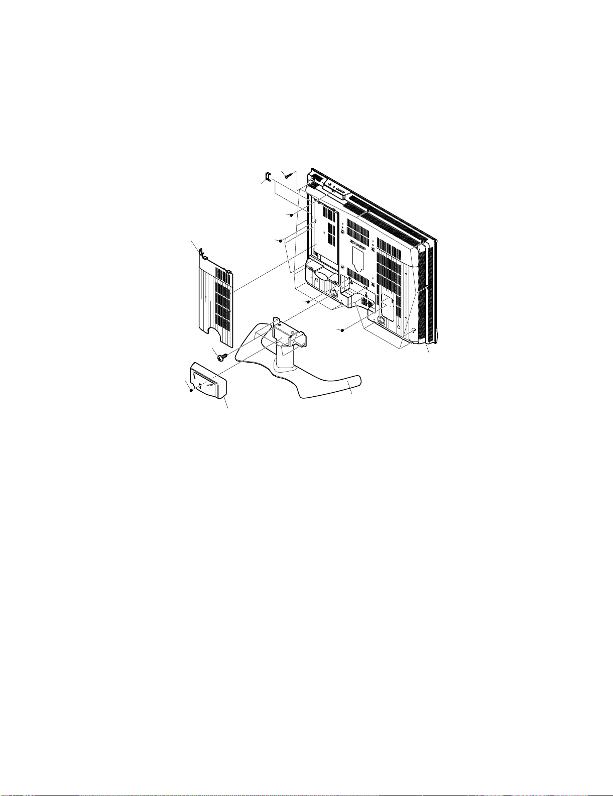
CHAPTER 4. REMOVING OF MAJOR PARTS
Service Manual
[1] REMOVING OF MAJOR PARTS
1. Detach the Terminal Cover [1].
2. Detach the 2 BUS Covers [2].
3. Remove the 1 screw [3] and detach the Hinge Cover.
4. Remove the 4 screws [4] and detach the Stand.
5. Remove the 3 screws [5], 4 screws [6] and the 12 screws [7]. Detach the Rear Cabinet.
[7]
BUS
[2]
Cover
[5]
Terminal
[1]
Cover
[6]
[5]
[3]
[6]
[4]
Rear
Cabinet
Stand
Hinge Cover
4 – 1
Page 9
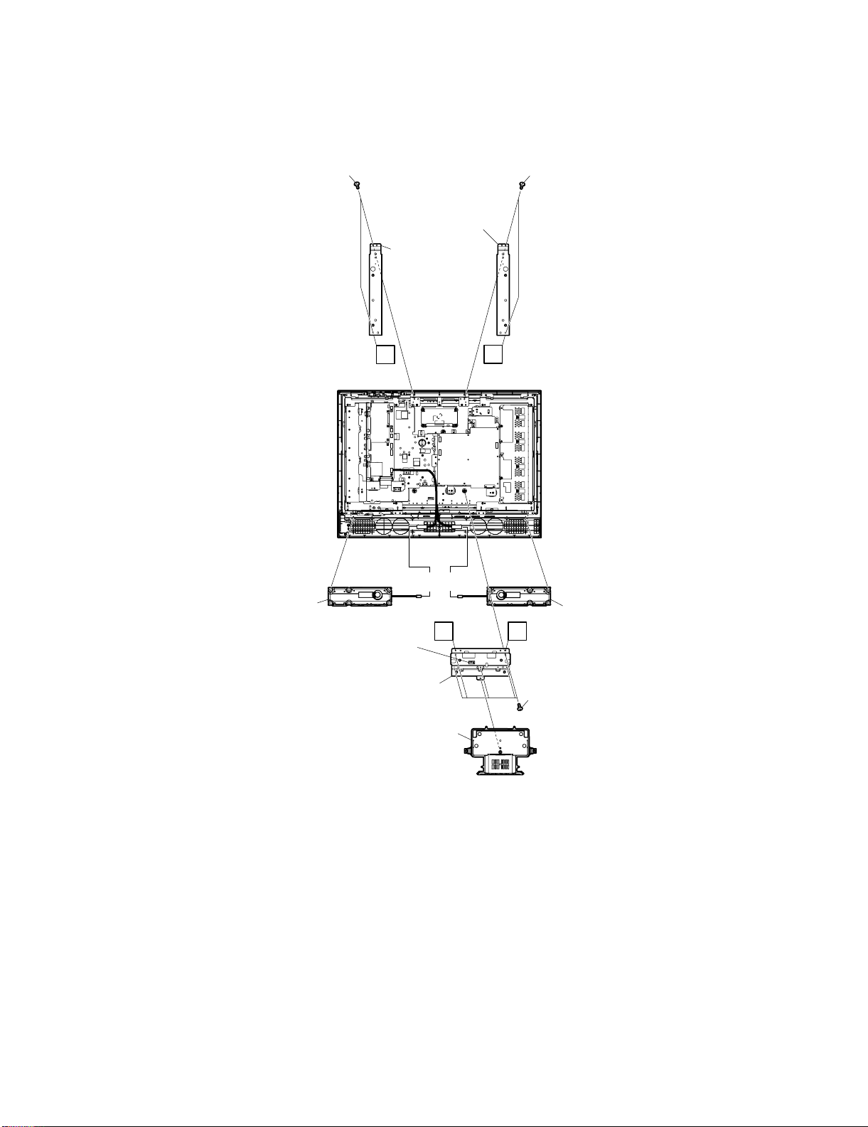
6. Detach the Stand Base Cover [8].
7. Remove the 4 screws [9]. Detach the SUS Angle-L and SUS Angle-R.
8. Disconnect the 2 Connectors [10]. Remove speaker wire from wire holder [10A].
9. Remove the 5 screws [11] and detach the Chassis Angle Bottom C.
10.Remove the Speaker Box L and Speaker Box R [12].
LC-32AX5H/M/X
[9]
SUS Angle-L
SUS Angle-R
A
[9]
B
[12]
Speaker
Box R
[10]
[10A] Wire holder
Chassis Angle Bottom C
[8]
Stand Base Cover
[10]
A
B
[11]
[12]
Speaker
Box L
4 – 2
Page 10

LC-32AX5H/M/X
11.Remove all the connectors from all the PWBs.
12.Remove the 2 screws [13] and detach the Top Control Cover Ass'y.
Remove the 2 screws [14] and detach the OPERATION PWB Unit from Top Control Cover Ass'y.
13.Remove the 2 screws [15] and detach the LED,R/C PWB Unit.
14.Remove the 2 screws [16] and detach the Side Hole Cover.
[13]
Top Control
Cover Ass'y
OPERATION
PWB Unit
[14]
Side Hole
Cover
[15]
SH
LV
KM
VD
RA
PD
PE
SP
LED,R/C PWB Unit
[KM]
CN2
CN1
CN3
[16]
4 – 3
Page 11
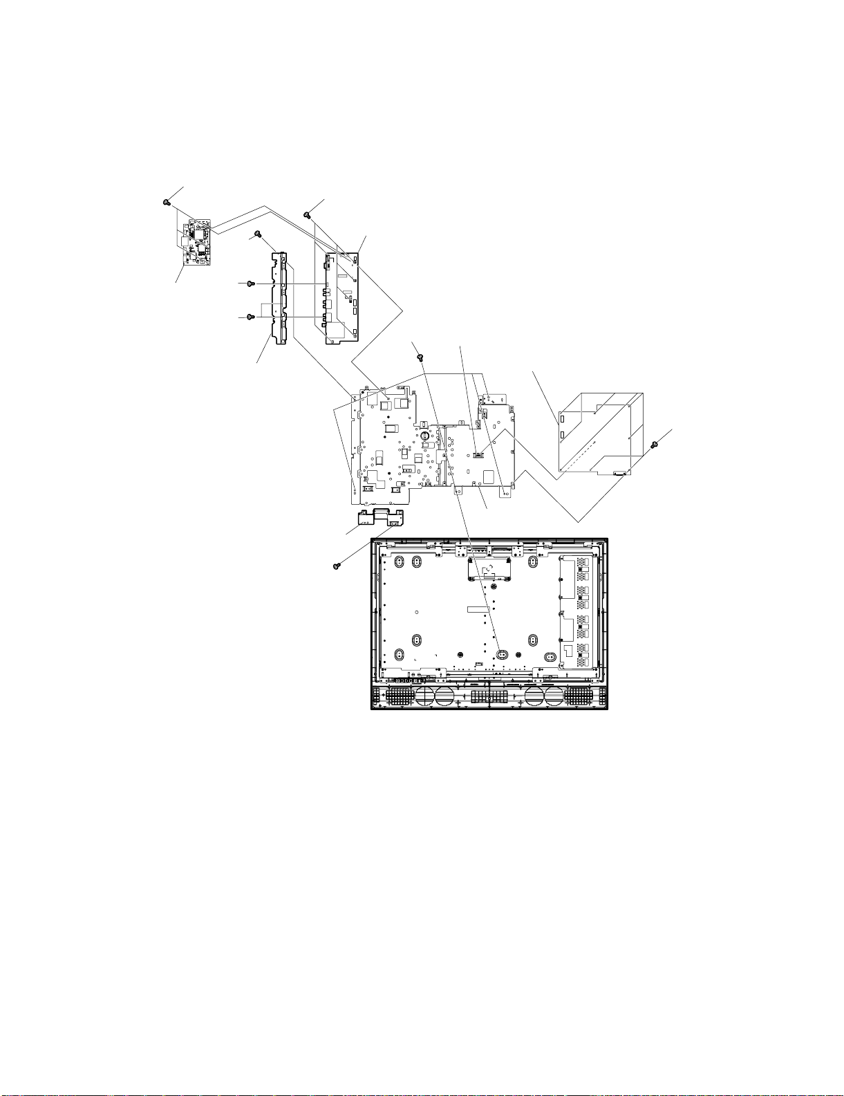
15.Remove the 1screw [17] and detach the Tuner Cover.
16.Remove the 5 screws [18] and detach Chassis Tray.
17.Remove the 2 screws [19] and the 1 screw [20]. Detach the AV Terminal Cover.
18.Remove the 8 screws [21] and the 1PWB holder C [21A], and detach the POWER PWB Unit from Chassis Tray.
19.Remove the 6 screws [22] and detach the SUB PWB Unit from Chassis Tray.
20.Remove the 3 screws [23] and detach the MAIN PWB Unit from SUB PWB Unit.
LC-32AX5H/M/X
[23]
AIN PWB
nit
[18]
[20]
[19]
AV Terminal
Cover
[22]
Tuner Cover
[17]
SUB PWB Unit
[18]
[21A] PWB Holder C
POWER PWB Unit
[21]
Chassis Tray
4 – 4
Page 12

LC-32AX5H/M/X
21.Remove the 4 screws [24] and take out the LCD Panel from Front Cabinet.
22.Remove the 11 screws [25] and detach the Chassis Angles.
[25]
[25]
[24]
[24]
Chassis Angle
Bottom R
[25]
Chassis Angle Top-C
[24]
Chassis Angle
Bottom L
[24]
[25]
Chassis Angle TopChassis Angle Top
[25]
4 – 5
Page 13

LC-32AX5H/M/X
LC-32AX5M
CHAPTER 5. ADJUSTMENT PROCEDURE
Service Manual
[1] ADJUSTMENT PROCEDURE
The adjustment values are set to their optimum at the factory before shipping. If by any chance a value should become improper or a readjustment is
required due to part replacement, make an adjustment according to the following procedure.
Before adjustment, perform aging for approx. 60 minutes to stabilize the unit.
1. Entering the adjustment process mode
1
While holding down the TV/VIDEO and Volume DOWN keys at the same time, set the Power switch to ON. (“K” standing for inspection process
mode is displayed in the upper left portion of the screen.) → Press the Channel DOWN and Volume DOWN keys at the same time. (The adjustment process mode screen appears.)
To cancel it, turn off the power using the Power switch or remote control.
2. Key operation in the adjustment process mode
1. Basic operations
• Tune in to a station using the Channel UP/DOWN keys.
• Switch the input using the TV/VIDEO key.
• Select an item to adjust using the Cursor / keys. (Pressing the Cursor key while at the bottom item moves to the top item on the
next page, and pressing the Cursor key while at the top item moves to the bottom item on the previous page.)
• Adjust the item selected using the Volume +/– or Cursor / keys.
• Press the Menu key to move to the next item. (Pressing the Menu key while at the bottom item moves to the top item on the next page.)
2. Layer movement
• Pressing the ENTER key while at an item other than I2C DATA and HOTEL POWERFIX on page 2 moves to the setting page of that item
name.
• Press the Flashback key to exit each setting page.
2
3. Initialization
3-1 Connect the pins 81 and 82 of IC2001 (microprocessor), then turn on the power.
3-2 Check MODEL (A648MB).
3-3 Check INCH SIZE.
MODEL INCH SIZE
LC-32AX5H/M/X 32
(Screen of adjustment process menu page 1)
0
123
0
1
2
3
4
5
6
7
8
M1ODE
INCH
ERROR
PUBL
HDCP
HDC
EXTTCONTROL
4 5 6 7 8 9 10 11 12 13 14 15 16 17 18 19 20 21 22 23 24 25 26
LA648MB
SIZE 32
NO RESE T
IC MODE OFF
40H 80
PRESETMODE 0
0
OFF
5 – 1
Page 14

LC-32AX5H/M/X
4. Adjustment
4.1. AD converter level adjustment
1. 1080i input
Adjustment Conditions Adjustment Procedure
1) 1080i 75% colour bar signal input
Used device name: LEADER LT448
Signal name: COLOUR BAR
* Use the LT-448-compatible third one of three color bars.
Setting value: 02: 1080i/59.93 (30 sF)
H: 33.72 kHz, V: 29.97 Hz
2. 480i input
Adjustment Conditions Adjustment Procedure
1) 480i 75% colour bar signal input
Used device name: LEADER LT448
Signal name: COLOUR BAR
* Use the LT-448-compatible third one of three color bars.
Setting value: 15: 480i/60
H: 15.73 kHz, V: 29.97 Hz
1) Set AUTO GAIN-OFFSET on page 3 (M2-HD) of the adjustment process DVP hierarchy to ON.
1) Set AUTO GAIN-OFFSET on page 4 (M2-SD) of the adjustment process DVP hierarchy to ON.
* If all the items are set to ON, “RUN” is displayed during adjustment.
5 – 2
Page 15
LC-32AX5H/M/X
4.2. TAMP adjustment
Adjustment Conditions Adjustment Procedure
1) Receive the PAL standard color bar signal. 1) If the maximum value of “PAL TAMP1” on page 1 of adjustment process DVP hierarchy is not in the range of values in the list below,
adjust “PAL TAMP1” on the same page so that the maximum value of
“Y” is in the range of values in the list below.
* Note that the setting value may vary by model.
2) When pressing the TAMP1 direct keys, adjustment of “PAL TAMP1”
is complete.
Then, The values of “NTSC TAMP1” and “SECAM TAMP1” are automatically set.
(NTSC: Value of PAL –7, SECAM: The same value as PAL)
MODEL 32AX5
Setting value 101 ~ 105
Reference
(Screen of page 1 of adjustment process menu DVP hierarchy)
0
0
DVP
1
2
3
4
5
6
7
8
9
10
11
12
13
14
15
1 2 3 4 5 6 7 8 9 10111213141516 1718192021 22 23242526
1
TAM 1L 10 1
YDA AT
TAM 1HP
NTS TAMP1C
PAL TAMP 1
P
103
105
88
95
CAM T AMP 1SE
95
5 – 3
Page 16
LC-32AX5H/M/X
4.3. White balance adjustment
1. White balance adjustment procedure
Adjust the white 144 gradation using RGB CUTOFF2 and then the white 73 gradation with RGB-GAIN.
1) Test signal adjustment
[Input signal] Display the WB test signals with built-in DVP of white 56% (144 gradations) and 29% (73 gradations) on the left and right of
[Adjustment value] Page 2 of adjustment process menu DVP hierarchy: RGB CUTOFF2, RGB-GAIN
the screen respectively by using the remote control code “011110010001010”.
Adjustment spec Inspection spec
White 56% x = 0.261 ±0.004 ±0.01 Radius from the center point
x = 0.277 ±0.004 ±0.01 Radius from the center point
White 29% x = 0.261 ±0.002 ±0.01 Radius from the center point
x = 0.277 ±0.002 ±0.01 Radius from the center point
[Adjustment method by bus]
Cutoff RGB CUTOFF2 G CUTOFF2 = Fixed to 0.
Vary RB CUTOFF2.
Gain RGB-GAIN G-GAIN = Fixed to 0.
Vary RB-GAIN.
(The adjustment value is measured with MINOLTA CA-210 and the correction mode is measured in the
mode compatible with CH02 “TOPCON”.)
Adjustment range: ±30
Adjustment range: ±30
5. MCL setting procedure
1. “MCL” is displayed in the upper left portion of the screen as shown in the figure below by sending the MCL key of the remote control for adjustment.
MCL
2. When the screen disappears after a few seconds and appears again, MCL setting is complete.
5 – 4
Page 17

LC-32AX5H/M/X
6. Factory setting
6.1. Performing the factory setting using the remote control for adjustment
1. Perform the factory setting using the remote control for adjustment. (This setting must be done after performing the MCL data setting.)
2. “H” standing for factory setting 1, “M” standing for factory setting 2 or “X” standing for factory setting 3 is displayed in the upper left portion of the
screen by continuing to press the Factory Setting key on the remote control for adjustment. (The figure below is the screen for factory setting 2.)
M
3. When “SETTING COMPLETE” is displayed in the middle of the screen after a few seconds, setting is complete.
M
SETTING COMPLETE
Model name Key name Remote control code Setting S-SYSTEM Set OSD language
LC-32AX5H Factory setting 1 (H) 100000111111110 I ENGLISH
LC-32AX5M Factory setting 2 (M) 100000001010110 B/G ENGLISH
LC-32AX5X Factory setting 3 (X) 100001001011110 B/G ENGLISH
4. Turn off the power.
NOTE: Set the Power switch to “OFF” immediately after completing the factory setting.
5 – 5
Page 18

LC-32AX5H/M/X
[2] PUBLIC MODE SETTING PROCEDURE
1. How to start Public Mode
• There are the following two ways to get the public mode setup screen displayed.
1
1) Press the “INPUT” and “VOL (+)” keys on the set at once and turn on the power.
2) Get the password input screen displayed.
Procedure
• The input starts with the leftmost digit.
• Use the numeric keys [1] thru [9] and [10/0] keys on the remote controller.
The other keys are not acceptable.
• With a numeric-key input, “–” will change to “ “. The input position will move one digit to the right.
• With all the 3 digits entered, the password will be verified.
3) The 3-digit password is now verified.
The password [0] [2] [7] provides for the public mode screen. (This screen comes on with whatever adjustment process settings.)
With any other passwords, the screen changes to the normal mode.
2
In the adjustment process mode, turn on “PUBLIC MODE”. Also press the “CH ( )” and “VOL (+)” keys on the set at once and turn on the power.
2. How to exit Public Mode
There are the following ways to quit the public mode setup screen.
• Turn off “PUBLIC MODE” in the adjustment process mode. ( ) ← This way alone is not for quitting the setup screen, but for quitting the mode
itself.
• Turn off the power with the “POWER” key. ( )
• Select “ENTER”. ( )
• Move the cursor to “RESET” and press the “FLASHBACK” key. (Back to the normal mode screen) ( )
••• “PUBLIC MODE” stays on in the adjustment process mode.
••• The settings will be back to the factory ones.
3. Public Mode Setting Values
• With the factory settings made, the public mode settings get initialized. (The adjustment process remains intact.)
5 – 6
Page 19

LC-32AX5H/M/X
4. Public Mode Menu
The guidance is not displayed onscreen.
Setup procedure
• To move the cursor up and down, use the “cursor UP/DOWN” key (remote controller) and “CH ( )/( )” key (remote controller and set).
• To change the settings, use the “cursor RIGHT/LEFT” key (remote controller) and “VOL (+)/(–)” key (remote controller and set).
• To save new settings, keep the cursor at “Enter” and use the “cursor RIGHT/LEFT” key (remote controller) and “VOL (+)/(–)” key (remote controller
and set).
Public mode
Power on fixed
Maximum volume
Volume fixed
Volume fixed level
RC button
Panel button
Menu button
On screen display
Input mode start
Input mode fixed
232C Powon
RC path through
Reset
Enter
5. On Setting Items
1. POWER ON FIXED
[Variable ]
[ 60]
[Variable ]
[ 20]
[Respond ]
[Respond ]
[Respond ]
[Yes ]
[Normal ]
[Variable ]
[Disable ]
[Off ]
Selection Variable/Fixed
Default Variable
Explanation When set to “Fixed”, the power cannot be turned off with the power key on the remote control or main unit, and the image
reception state is kept (it does not enter the standby state).
The power can be turned off by shutting off power supply from AC.
Limit in setting • Power key on the main unit/remote control power supply key
• OFF timer/ON timer
Exception None
Remarks • Selection of “FIXED” assumes use of STB, etc.
• When set to “Variable”, if the main power switch is set to off, the power is turned off after a wait of 1 second.
(Push-push switch only)
• Display ON/OFF in the hotel menu is controlled by the adjustment process “HOTEL POWERFIX”.
• When the power button is operated, a caution is displayed (it times out in 5 seconds).
(For the caution, refer to the power on fixed message sheet.)
* The caution is not displayed when in the adjustment process, hotel menu, default setting, MCL operation and auto preset
(Ch search operation).
The OSD display including the menu and this caution have priority over all others.
When “OSD display” (described below) is set to “Variable”, this caution is displayed as a special case.
2. MAXIMUM VOLUME
Selection Adjustment from 1 to 60 (no loop)
Default 60
Explanation Sound volume can not be adjusted higher than the preset value.
Limit in setting • When the sound volume is set lower than 59, only figures are displayed and the sound volume bar is not displayed.
• The maximum sound volume for ON-timer (Wake up timer) is limited also to the preset value.
Exception • In the item “VOLUME” of adjustment process, the sound volume can be set freely irrespective of this setting.
Remarks • Setting is valid only for the speakers of the unit. (As for the headphone, the sound volume can be set up to 60 irrespective
of the limit.)
• In line output (sound volume variable), the sound volume can be adjusted from -60 to 0 irrespective of pre-adjusted value.
• When the sound volume is set higher than the MAX setting by the adjusting process or headphone, the sound volume con-
trol operation is prohibited for turn-up and the sound volume should be turned down to MAX in this state.
5 – 7
Page 20

LC-32AX5H/M/X
3. VOLUME FIXED
Selection Selection between “Variable” and “Fixed” (loop provided)
Default Variable
Explanation Sound volume is fixed and made invariable.
Limit in setting • The sound volume for the ON-timer (Wake up timer) is fixed also without display of menu. Besides, the setting is made
Exception • In the item “VOLUME” of adjustment process, the sound volume can be set freely irrespective of this setting.
Remarks • In “Variable” setting, the sound volume had been conventionally set at 1 but this operation has been abolished (and follows
4. VOLUME FIXED LEVEL
Selection Adjustment from 1 to 60 (no loop)
Default 20
Explanation The sound volume to be fixed by “Volume fixed” is determined.
Limit in setting None
Exception None
Remarks Setting is valid only when “Volume fixed” is selected for “fixed”.
impossible. (Basically, the menu is not displayed.)
• The following keys become invalid:
1) Sound volume Up/Down (VOL +/-) [for both remote control and the unit]
2) Mute (MUTE)
the last memory).
• The sound volume for the ON-time is not set at 1 either and the sound volume set value of the ON-timer before executing
the hotel mode is held.
• Setting is valid only for the speakers of the unit. (As for the headphone, the sound volume can be set up to 60 irrespective
of the limit.)
• In line output (sound volume variable), the sound volume can be adjusted from -60 to 0 irrespective of pre-adjusted value.
• As for sound volume fixing and sound volume MAX level, the sound volume fixing has priority.
• Once the sound volume has been changed by adjustment process or headphone, it should be set back to the sound volume
preset by sound volume fixing level when the adjustment process ends or when the headphone is removed.
This must be confirmed actually by changing also the sound volume in accordance with setting.
5. R/C BUTTON
Selection Selection between “Respond”, “Limited” and “No respond” (loop provide)
Default Respond
Explanation Keys acceptable by remote control are limited or reception of keys can be prohibited.
Limit in setting 1) In “limited” setting, only power ON/OFF, sound volume , tuning and BACKLIGHT (brightness sensor) are
accepted.
2) In “No respond” setting, all the keys (including the power key) are not accepted.
Exception • Adjustment process, factory setting, inspection process and hotel only keys are valid irrespective of setting.
Remarks
6. PANEL BUTTON
Selection Selection between “Respond” and “No respond” (loop provide)
Default Respond
Explanation All the operations by keys (except the power key) of the unit can be invalidated.
Limit in setting
Exception • Inspection mode and hotel menu mode can be started irrespective of setting.
Remarks
7. MENU BUTTON
Selection Selection between “Respond” and “No respond” (loop provide)
Default Respond
Explanation In “No respond” setting, the menu operation by the menu key of the remote control and the menu key of the unit are invali-
Limit in setting • ON-timer (Wakeup Timer) is turned OFF.
Exception • Inspection mode and hotel menu mode can be started irrespective of setting.
Remarks
• All the keys can be used in adjustment process, inspection mode and hotel menu irrespective of setting.
• All the keys can be used in adjustment process, inspection mode and hotel menu irrespective of setting.
dated.
• The following keys become invalid.
Wake-up timer and clock setting keys and all of the direct change keys to menu display
• All the keys can be used in adjustment process, inspection mode and hotel menu irrespective of setting.
5 – 8
Page 21

LC-32AX5H/M/X
8. ON SCREEN DISPLAY
Selection Selection between “Yes”, “Limited” (loop provide)
Default Yes
Explanation The following OSD displays are made ineffective.
Displays of menu group, channel call, sound volume bar and direct key call
Limit in setting • Set time of the OFF-timer (SLEEP TIMER) is cleared.
• Setting of the no-signal power-OFF (AUTO POWER OFF) is cleared to “OFF”.
• Setting of the no-operation power-OFF is cleared to “OFF”.
• Keys falling under any of the following items become invalid.
1) Appearance of screen changes and the sound changes.
2) Personal functions which are hard to restore.
Ex.) Screen display, menu, OFF-timer, ON-timer, AV MODE, screen size switching, clock setting, treble emphasis, AUDIO
ONLY, sound changeover, LANGUAGE, CLOSED CAPTION
Others • Simple input switching is generated. Those which are restored soon after leaving as they are and may be requested for
change by customer are not prohibited.
Ex.) Brightness sensor (BACKLIGHT) and PIC. FLIP
Exception • Such a caution which is displayed independently is displayed as it is.
9. INPUT MODE START
Selection Selection between “Normal”, “TV (CH~)” “INPUT1~5”, “PC” (loop provide)
Default Normal
Explanation In power-ON, the input source to be started or channel can be set.
About options • All the input sources in the model are made selectable.
Limit in setting • The display of channel setting menu and the channel setting operation are prohibited (except for MCL).
Exception None
Remarks • In setting at “Normal”, the setting of “Input mode fixed” is changed to “Variable” and selection should be prohibited.
10.INPUT MODE FIXED
Selection Selection between “Variable” and “Fixed” (loop provide)
Default – (Variable)
Explanation The input mode is fixed at the input source or the channel set at the “Input mode start” in 9 and other input sources and chan-
Limit in setting • With the execution of hotel mode, the input source is forced to change to that set by “Input mode start” and the channel
Exception None
Remarks • In the following case, setting is cancelled and mode is changed to “Variable”.
11.232C POWON
Non-responding signal caution, TELE TEXT caution and power-ON fixing caution
(In standard mode, the operation follows the last memory.)
• When the input/output switchable input source is selected and the input source is set to output, the setting of input/output
switching is changed to input at the execution of hotel menu. In addition, the input/output switching by menu is prohibited.
• In TV mode, the display of all channels is stopped and it is treated as an input source. At this time, the channel to be set fol-
lows the last memory and the content of the last memory is included in the notation by options. Ex.) TV (CH2), TV (CH4)
etc.
• The order of appearance of options in the hotel menu should agree with the order of toggles by input switching key.
nels can be made non-selectable.
switching and input switching are prohibited thereafter.
• The following keys are invalidated.
CH , direct tuning button, FLASHBACK, input
*However, the keys (input switching and CH keys) of the unit for menu operation remain valid.
1
When the setting of “Input mode start” is set to “Standard (Normal)”
Selection “Enable” and “Disable”
Default Disable
Explanation When in the standby state, power ON by the RS-232C command is enabled or disabled.
Limit in setting None
Exception None
Remarks It is irrelevant to power OFF by the RS-232C command.
5 – 9
Page 22

LC-32AX5H/M/X
12.RC PATH THROUGH
Selection “Off”, “On: TV RCE”, “On: TV RCD”
Default Off
Explanation Remote control signal output from the pin 9 of the RS-232C terminal and signal reception by is enabled or disabled.
When set to “ON: TV RCE”, TV also receives signals. With “ON: TV RCD”, the remote control signal is output from the pin 9,
but TV does not respond to the remote control.
Limit in setting When set to “ON: TV RCD”, TV does not accept the remote control.
Exception None
Remarks
RS-232C power ON command “POWR1_ _ _ ”
5 – 10
Page 23

LC-32AX5H/M/X
LC-32AX5M
CHAPTER 6. TROUBLESHOOTING TABLE
Service Manual
[1] TROUBLESHOOTING TABLE
No power (front LED failure to light up) or no startup (front LED failure to turn from red to green)
Is the AC cord connector tightly connected to the set? NO Reconnect the AC cord tightly and turn on the power again.
YES
Is the output voltage at pin (5) of P5011 (BU+5V line) as specified?
YES
Are the wire harnesses and other cables properly connected in
the set?
YES
Is there the PS ON and PNL_POW signal input at pin (1) and (4)
of P5011 (PS ON line)?
YES
Is the output voltage of each pin on P5010 as prescribed?
Pin 1 6V
Pins 3 and 4 5V
Pins 7 and 8 10V
Pins 11 and 12 13V
NO Replace the power unit (RDENCA182WJQZ).
NO Reconnect the wire harnesses and other cables properly in the
set.
NO Check the PS ON signal line PNL_POW signal line.
NO Replace the power unit (RDENCA182WJQZ).
YES
Are the DC/DC converter outputs and the output voltages along
the control lines as specified?
1) 5V (IC707 etc.)
2) 4V (IC703, Q707 etc.)
3) 3.3V (IC702, Q706 etc.)
4) 1.5V (IC704, Q708 etc.)
5) 8.5V (IC705 etc.)
6) 31V (IC706 etc.)
NO Check the DC/DC converters and the control lines. Replace
defective parts as required.
6 – 1
Page 24

LC-32AX5H/M/X
With <Video> signal input No video onscreen (1)
No external input video onscreen <INPUT 1>
Is INPUT 1 selected on the input select menu screen? NO Select INPUT 1 on the input select menu screen to pick up the
right input signal.
YES
Is there the video signal input at pin (1) of IC3408 (AV SWITCH)? NO Check the line between pin (8) of J3404 and pin (1) of IC3408.
YES
Is there the video signal output at pin (7) of IC3408? NO Check IC3408 and its peripheral circuits.
YES
Is there the video signal input at U2 pin of IC801? NO Check Q3404 and its peripheral circuits.
YES
Are signals output from the pins P22, P23, R22, R23, T22, T23,
U22, U23, V22, and V23 of IC801 normally?
NO Check IC801 and its peripheral circuits.
YES
Check LVDS cable, LCD controller (incl. panel) and their peripheral circuits.
With <Video> signal input No video onscreen (2)
No external input video onscreen <INPUT 2>
Is INPUT 2 selected on the input select menu screen? NO Select INPUT 2 on the input select menu screen to pick up the
YES
Is there the video signal input at pin (3) of IC3408 (AV SWITCH)? NO Check the line between pin (1) of J3405 and pin (3) of IC3408.
YES
Is there the video signal output at pin (7) of IC3408? NO Check IC3408 and its peripheral circuits.
YES
Is there the video signal input at U2 pin of IC801? NO Check Q3404 and its peripheral circuits.
right input signal.
YES
Are signals output from the pins P22, P23, R22, R23, T22, T23,
U22, U23, V22, and V23 of IC801 normally?
YES
Check LVDS cable, LCD controller (incl. panel) and their periph-
eral circuits.
NO Check IC801 and its peripheral circuits.
6 – 2
Page 25
LC-32AX5H/M/X
With <Component> signal input No video onscreen (3)
No external input video onscreen <INPUT 1>
Is INPUT 1 selected on the input select menu screen? NO Select INPUT 1 on the input select menu screen to pick up the
right input signal.
YES
Are there the Y, Pb and Pr signal inputs at pins (25), (1) and (5)
of IC3402 (Component SW), respectively?
YES
Is input waveform of IC802 normal?
Y=U1pin, Sync=J2pin
Pb=L1pin, Pr=R1pin
YES
Are there the signal outputs at pins U22, U23, V22, V23, P22,
P23, R22, R23, T22, T23 of IC801, respectively?
YES
Check LVDS cable, LCD controller (IN PANEL) and their periferal
circuits.
NO Check the line between pins (10)/(6)/(4) of J3404 and pins (25)/
(1)/(5) of IC3402.
NO Check IC3402 and its peripheral circuits.
NO Check IC801 and its peripheral circuits.
With <Component> signal input No video onscreen (4)
No external input video onscreen <INPUT 3>
Is INPUT 3 selected on the input select menu screen? NO Select INPUT 3 on the input select menu screen to pick up the
YES
Are there the signal inputs from the HDMI (SC403) connector to
the following input terminals of IC8702 (pin (16), (17), (19), (20),
(22), (23), (25), (26)).
YES
Are there the clock, H, V, Data signal outputs at pins (71) - (78),
(83) - (90), (96), (98), (99), (104) - (111) of IC8702, respectively?
YES
Are there the signal outputs at pins U22, U23, V22, V23, P22,
P23, R22, R23, T22, T23 of IC801, respectively?
YES
Check LVDS cable, LCD controller (IN PANEL) and their peripheral circuits.
NO With an HDMI device connected, is IC404 (EEPROM) accessed
NO Check IC8702, IC8703 and their peripheral circuits.
NO Check IC801 and its peripheral circuits.
right input signal.
by I2C and is the DDC I2C CLOCK/DATA data read?
NO
Check IC404 and their peripheral circuits.
6 – 3
Page 26

LC-32AX5H/M/X
No audio heard (1)
No sound in the UHF/VHF reception.
Is the IF output from the tuner pin (14) of TU3401 as specified? NO Check TU3401 and its peripheral circuits.
YES
Is the SIF signal input at A21 pin of IC801 as specified? NO Check Q3414, Q3415 and their peripheral circuits.
YES
Are audio signals from the pins B23 and D23 of IC801 as
prescribed?
YES
Is there the L-ch audio signal output at pins (53) of IC1301? NO Check IC1301 and its peripheral circuits.
Is there the R-ch audio signal output at pins (54) of IC1301?
YES
Is there the L-ch audio signal output at pins (20), (21) of IC1303
(AMP)?
Is there the R-ch audio signal output at pins (40), (41) of IC1303
(AMP)?
NO Check IC801 and their peripheral circuits.
NO Check IC1303 and its peripheral circuits.
YES
Are audio signals of L-ch and R-ch output from the pins (1)/(2)
and (3)/(4) of P5007 normally?
YES
Check the speakers and their peripheral circuits.
No audio heard (2)
No external audio heard
<INPUT 1>
Is there the L-ch audio signal input from pin (11) of input terminal
J3404 to pin (56) of IC1301?
Is there the R-ch audio signal input from pin (13) of input terminal
J3404 to pin (57) of IC1301?
<INPUT 2>
Is there the L-ch audio signal input from pin (4) of input terminal
J3405 to pin (50) of IC1301?
Is there the R-ch audio signal input from pin (6) of input terminal
J3405 to pin (51) of IC1301?
YES
Is there the L-ch audio signal output at pins (20), (21) of IC1303
(AMP)?
Is there the R-ch audio signal output at pins (40), (41) of IC1303
(AMP)?
NO Check IC1301 and its peripheral circuits.
NO Check IC1303 and its peripheral circuits.
YES
Are audio signals of L-ch and R-ch output from the pins (1)/(2)
and (3)/(4) of P5007 normally?
YES
Check the speakers and their peripheral circuits.
6 – 4
Page 27

No audio heard (3)
No audio signal at the monitor audio output terminal.
Is there the L-ch audio signal output at pin (37) of IC1301? NO Check IC1301 and its peripheral circuits.
Is there the R-ch audio signal output at pin (36) of IC1301?
YES
Does the audio mute circuit function?
(Q3401, Q3402 and Q3403)
YES
Check the monitor audio output terminal (J3405) and its
peripheralcircuits.
No audio heard (4)
No sound heard from the headphone.
Is there the audio signal output at pins (28) (L-ch) and (27) (R-ch)
of IC1301?
NO Check Q3401, Q3402, Q3403, pin (58) of IC2001 and their
peripheral circuits.
LC-32AX5H/M/X
Is there the L-ch audio signal output at pin (3) of IC1302
(H/P AMP)?
Is there the R-ch audio signal output at pin (5) of IC1302
(H/P AMP)?
YES
Check J101, IC1901, IC1902 and it peripheral circuits, as well as
the headphone jack line.
NO Is the mute signal input at pin (2) of IC1302 as specified?
6 – 5
Page 28
LC-32AX5H/M/X
No audio heard (5)
No HDMI sound heard.(INPUT 3 is digital audio.)
Does the HDMI image appear onscreen? NO Refer to “<INPUT 3> in No external image onscreen (HDMI)”.
YES
No audio output from INPUT 3. NO Check if the EDID data of IC404 (INPUT 3) is normal.
YES
YES
Are waveforms of the pins (120) - (124) of IC8702 output
normally?
YES
Are output waveforms of the audio output pins B23 and D23 of
IC801 normal?
NO Check peripheral circuits of IC8702.
NO Check peripheral circuits of IC801.
Check peripheral circuits of IC404.
YES
Are audio signals of L-ch and R-ch input in to the pins (53) and
(54) for volume, equalizer and sound of IC1301 normally and
output from the pins (28) and (27) normally?
YES
Are there the L-ch and R-ch audio signal outputs at pins (20),
(21) and (40), (41) of IC1303 (AMP), respectively?
YES
Are there the L-ch and R-ch audio signal inputs at pins (1), (2)
and (3), (4) of P5007, respectively?
No audio heard (6)
No sound from the HDMI sound input terminal.
(INPUT 3 analog audio)
YES
Is there the L-ch audio signal input from pin (4) of external input
terminal J3401 (HDMI AUDIO IN) to pin (47) of IC1301?
Is there the R-ch audio signal input from pin (2) of external input
terminal J3401 (HDMI AUDIO IN) to pin (48) of IC1301?
YES
Are audio signals of L-ch and R-ch of IC1301 normally and out-
put from the pins (28) and (27) normally?
NO Check peripheral circuits of IC1301.
NO Check IC1303 and its peripheral circuits.
NO Check peripheral circuits of IC1301.
YES
Are there the L-ch and R-ch audio signal outputs at pins (20),
(21) and (40), (41) of IC1303 (AMP), respectively?
YES
Are there the L-ch and R-ch audio signal inputs at pins (1), (2)
and (3), (4) of P5007, respectively?
NO Check IC1303 and its peripheral circuits.
6 – 6
Page 29

LC-32AX5M
CHAPTER 7. MAJOR IC INFORMATIONS
Service Manual
[1] MAJOR IC INFORMATIONS
1. IC801 (IXB880WJ)
Outline
DVP-M2S is a 1-chip video signal processing LSI for flat panel display supporting multi-format (NTSC/PAL/SECAM).
BLOCK DIAGRAM
LC-32AX5H/M/X
MCU
IC2001
AV SW
IC
VHINJM2246M-1Y
COMPONENT SW
VHISM5301CS-1Y
POWER
3.3V 1.5V
UART
V
OUT
Y/Pb/Pr
27MHz
Xtal
RH-IXB880WJZZQ
IC801
DVP-M2
S_IF
SIF AMP
Q
OFL_PWM
LV_PCLK
LV_R/G/B
I2S
MODULE
L/R
Volume/EQ/HP/
Surround
HDMI Receiver
MST3383
IC8702
LCD
Audio
7 – 1
Page 30
LC-32AX5H/M/X
Terminal assignment (TOP VIEW)
7 – 2
Page 31

LC-32AX5H/M/X
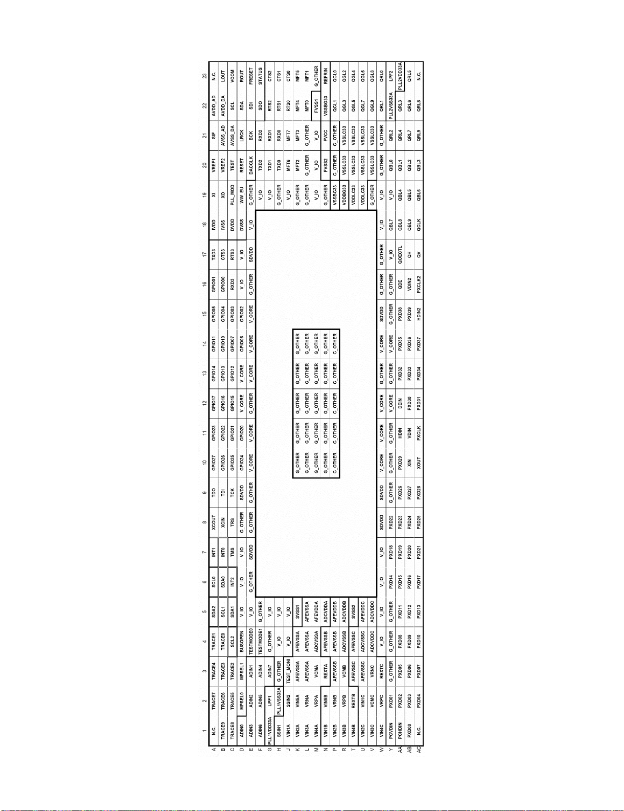
Terminal function description
Terminal No. Pin name I/O Function Connection Signal
AA2 PXD02 I Digital video signal input 02 (A) R02
AB2 PXD03 I Digital video signal input 03 (A) R03
AC2 PXD04 I Digital video signal input 04 (A) R04
AA3 PXD05 I Digital video signal input 05 (A) R05
AB3 PXD06 I Digital video signal input 06 (A) R06
AC3 PXD07 I Digital video signal input 07 (A) R07
AA4 PXD08 I Digital video signal input 08 (A) R08
AB4 PXD09 I Digital video signal input 09 (A) R09
AB5 PXD12 I Digital video signal input 12 (A) G02
AC5 PXD13 I Digital video signal input 13 (A) G03
Y6 PXD14 I Digital video signal input 14 (A) G04
AA6 PXD15 I Digital video signal input 15 (A) G05 8 bit
AB6 PXD16 I Digital video signal input 16 (A) G06 R/G/B
AC6 PXD17 I Digital video signal input 17 (A) G07
Y7 PXD18 I Digital video signal input 18 (A) G08
AA7 PXD19 I Digital video signal input 19 (A) G09
Y8 PXD22 I Digital video signal input 22 (A) B02
AA8 PXD23 I Digital video signal input 23 (A) B03
AB8 PXD24 I Digital video signal input 24 (A) B04
AC8 PXD25 I Digital video signal input 25 (A) B05
AA9 PXD26 I Digital video signal input 26 (A) B06
AB9 PXD27 I Digital video signal input 27 (A) B07
AC9 PXD28 I Digital video signal input 28 (A) B08
AA10 PXD29 I Digital video signal input 29 (A) B09
A21 SIF I Sound multiplex decoder SIF input S_IF SIF
B23 LOUT O Sound multiplex decoder L-ch analog output DVPM2_L
D23 ROUT O Sound multiplex decoder L-ch analog output DVPM2_R
D21 LRCK I/O Sound multiplex decoder LR clock I2S_WS
E21 BCK I/O Sound multiplex decoder bit clock I2S_CLK
E22 SDI I/O
J20
P23 QGL0/TXOUT0M O
P22 QGL1/TXOUT0P O
R23 QGL2/TXOUT1M O
R22 QGL3/TXOUT1P O
T23 QGL4/TXOUT2M O
T22 QGL5/TXOUT2P O
U23 QGL6/TYCLKOUTM O
U22 QGL7/TYCLKOUTP O
V23 QGL8/TYOUT3M O
V22 QGL9/TYOUT3P O
L1 VIN3A I A-ch Analog video input 3 COMP1_Pb Pb
K2 VIN5A I
N1 VIN1B I
R1 VIN3B I B-ch Analog video input 3
N2 VIN5B I
GP1036/MFT6A/
MFT7B
Built-in sound multiplex decoder
Digital input for A/D converter
General-purpose input/output port GP1036/
I/O
MFT6A input/MFT7B input/output
Pulse signal output G0/LVDS 0-ch Inverted output
(Connection to TXOUT0P via 100 Ω)
Pulse signal output G1/LVDS 0-ch Output
(Connection to TXOUT0M via 100 Ω)
Pulse signal output G2/LVDS 1-ch Inverted output
(Connection to TXOUT1P via 100 Ω)
Pulse signal output G3/LVDS 1-ch Output
(Connection to TXOUT1M via 100 Ω)
Pulse signal output G4/LVDS 2-ch Inverted output
(Connection to TXOUT2P via 100 Ω)
Pulse signal output G5/LVDS 2-ch Output
(Connection to TXOUT2M via 100 Ω)
Pulse signal output G6/LVDS Inverted clock
(Connection to TXCLKOUTP via 100 Ω)
Pulse signal output G7/LVDS Clock
(Connection to TXCLKOUTM via 100 Ω)
Pulse signal output G8/LVDS 3-ch Inverted output
(Connection to TXOUT3P via 100 Ω)
Pulse signal output G9/LVDS 3-ch Output
(Connection to TXOUT3M via 100 Ω)
A-ch Analog video input 5
NOTE: Only the B signal of SCART input can be input.
Other video signals can not be input.
B-ch Analog video input 1
NOTE: The R signal is connected on SCART input.
B-ch Analog video input 5
NOTE: Only the FB signal of SCART input can be input.
Other video signals can not be input.
I2S_DA_TO_DVP
INV_OFL OFL_PWM
TX_OUT0-_L
TX_OUT0+_L
TX_OUT1-_L
TX_OUT1+_L
TX_OUT2-_L
TX_OUT2+_L
TX_C_KOUT-_L
TX_C_KOUT+_L
TX_OUT3-_L
TX_OUT3+_L
COMP1_Pr Pr
L/R
I2S
LV_ PCLK/
LV_R/G/B
7 – 3
Page 32

LC-32AX5H/M/X
Terminal No. Pin name I/O Function Connection Signal
J1 VIN1A I
U1 VIN2C I C-ch Analog video input 2.
U2 VIN1C I C-ch Analog video input 1. SVBS1 VOUT
P1 VIN2B I B-ch Analog video input 2. SY1 YOUT
K1 VIN2A I A-ch Analog video input 2. SC1 COUT
T1 VIN4B I B-ch Analog video input 4. PC_R
V1 VIN3C I C-ch Analog video input 3. PC_G PC_R/G/B
M1 VIN4A I A-ch Analog video input 4. PC_B
Y1 PCVDIN I Vertical sync signal on analog PC input M2_PC_V PC_H/V
AA1 PCHDIN I Horizontal sync signal on analog PC input M2_PC_H
F20 GPIO52/TYD2/MSQ I/O
F21 GPIO53/RYD2/MSD I/O
AB10 XIN I Oscillation buffer input fir system clock
A-ch Analog video input 1
Note: The G signal is connected on SCART input.
General_purpose input/output port GPIO52/when
BUSOPEN= “L”, MPSEL0= “L”, MPSEL1= “L” or
BUSOPEN= “H”, MPSEL0= “L”, MPSEL1= “H”.
UART2 or CSIO2 transmission data.
4-wire serial data output MSQ when BUSOPEN= “H”,
MPSEL= “H”, MPSEL1= “L”.
General_purpose input/output port GPIO53/when
BUSOPEN= “L”, MPSEL0= “L”, MPSEL1= “L” or
BUSOPEN= “H”, MPSEL0= “L”, MPSEL1= “H”.
UART2 or CSIO2 transmission data.
4-wire serial data output MSD when BUSOPEN= “H”,
MPSEL= “H”, MPSEL1= “L”.
COMP1_Y Y
DVP_TXD
UART
DVP_RXD
7 – 4
Page 33

LC-32AX5H/M/X
2. IC1301 (IXB302WJ)
• IC1301 (IXB302WJ) Signal Flow Description
• The INPUT3 (HDMI) signals are input into IC801 via IC8702. The tuner SIF signal is input into IC801 and is processed by the sound multiplex
decoder. HDMI or tuner is selected at IC801 and is input into the pins 53/54 of IC1301.
• INPUT1/INPUT2/INPUT3 are input into the pins 47/48/50/51/56/57 of IC1301.
• Tuner, INPUT1/INPUT2/INPUT3 and INPUT3 Audio are selected at IC1301.
• The speaker sound is output from the pins 27/28 of IC1301.
• The headphone sound is output from the pins 27/28 of IC1301.
• The monitor output sound is output from the pins 36/37 of IC1301.
• Power sources are digital +5V (pins 12 and 13), analog +5V (pins 65 and 66) and +8V (pin 39).
• The oscillator circuit employs X’tal (18.432 MHz) (pins 71 and 72).
•I2C control
• The following functions incorporated: Source Selector, Surround, Volume, Bass/Treble, Balance, 7Band GEQ, and 3Band PEQ
BLOCK DIAGRAM
Pin assignment
INPUT3
(HDMI)
SIF
TMDS
VHIMST3383M-1Q
RH-IXB880WJZZQ
ANA
IC8702
HDMI Reciever
I2S
IC801
VIDEO/AUDIO
Decoder
INPUT1
INPUT2
INPUT3
ANA
ANA
IC1301
RH-IXB302WJN1Q
Audio Processor
Fuction
Source Selector
Surround
Volume
Bass/Treble
Balance
7Band GEQ
3Band PEQ
LINE INPUT SELECT
A/D
Prescale
SOURCE SELECT
Loud Speaker
Sound Processing
ANA
VHITPA3100D-1Y
Audio Amp
ANA
VHIBH3544F+-1Y
H-Amplifier
IC1303
IC1302
ANA
SP
OUT
HP
OUT
MONITOR
OUT
IC1301
IXB302WJ
D/A D/A
Line Out
Select
BLOCK DIAGRAM of the AUDIO PROCESSOR
7 – 5
Page 34

LC-32AX5H/M/X
3. IC8702 (MST3383)
Features
• Highly integrated HDMI interface for 25-170 MHz pixel rates
• Compatible with VGA through UXGA RGB graphics signals, and component TV, DTV and HDTV
• Two DVI/HDMI single link inputs
• HDMI 1.0 compliant
• Smart sync detection with HSYNC, VSYNC and DE period report
• Serial port programming interface
HDMI Interface
• 25 MHz - 170 MHz operation
• Supports HDMI 1.0 (High Definition Multimedia Interface) and is compatible with HDMI 1.1
• Supports High bandwidth Digital Content Protection. HDCP 1.1
• Backward compatible to DVI 1.0
• Supports up to 25-meter cable
• Supports encrypted video contents
• Supports authentication of video receiver with decryption of encoded data at the receiver
Digital Audio Output Interface
• Supports up to 2-channel serial audio output
• Supports S/PDIF digital audio output
• Supports audio sample rates of 32-192kHz, with a sample size of 16-24 bits
Digital Video Output Interface
• Supports color space conversion and sRGB
• Supports 24-bit 4:4:4 YCbCr/RGB output formats
• Supports 16-bit 4:2:2 YCbCr output formats (ITU.601)
• Supports 8-bit 4:2:2 YCbCr output formats (ITU.656)
BLOCK DIAGRAM
MCL MDA
DDCB SCL
DDCB SCA
HDMI Link B
HDMI
RX
HDCP Cipher
XOR Mask
24
24
Test Pattern
Generator
24 24
MUX
CSC
Audio
Stream
Output
Formatting
Serial Audio Bus
SPDIF Out
FIELD
VSOUT
HSOUT
DE
DATACK
DATA[23:0]
Sync
Processing
Host Interface
and
Power Management
SCL SDA A0 XIN XOUT
Clock
Generator
7 – 6
Page 35

Pin assignment
NC
NC
NC
NC
NC
NC
NC
NC
NC
LC-32AX5H/M/X
NC
MST3383M
7 – 7
Page 36

LC-32AX5H/M/X
Pin description
CPU Interface
Pin Name Pin type Function Pin
HWRESET Schmitt Trigger Input w/ 5V-tolerant Hardware Reset; Active High 63
A0 Input w/ 5V-tolerant Serial Interface Address Input 64
SCL Input w/ 5V-tolerant 2-Wire Serial Bus Clock 65
SDA I/O w/5V-tolerant 2-Wire Serial Bus Clock 66
INT Output w/Pull-Down Resister CPU Interrupt Programmable By User 68
DVI/HDMI Interface
Pin Name Pin type Function Pin
RXB0N DVI/HDMI Input Negative DVI/HDMI Input for B Link Data Channel 0 16
RXB0P DVI/HDMI Input Positive DVI/HDMI Input for B Link Data Channel 0 17
RXB1N DVI/HDMI Input Negative DVI/HDMI Input for B Link Data Channel 1 19
RXB1P DVI/HDMI Input Positive DVI/HDMI Input for B Link Data Channel 1 20
RXB2N DVI/HDMI Input Negative DVI/HDMI Input for B Link Data Channel 2 22
RXB2P DVI/HDMI Input Positive DVI/HDMI Input for B Link Data Channel 2 23
RXBCKN DVI/HDMI Input Negative DVI/HDMI Input for B Link Clock Channel 25
RXBCKP DVI/HDMI Input Positive DVI/HDMI Input for B Link Clock Channel 26
Misc. Interface
Pin Name Pin type Function Pin
XOUT Crystal Oscillator Output 61
XIN Crystal Oscillator Input 62
MCL Output w/ 5V-tolerant HDCP Master Serial Bus Clock 69
MDA I/O w/ 5V-Tolerant HDCP Master Serial Bus Data I/O 70
REXT External Resistor 390 Ohm connected to AVDD_DVI 28
DDCBSCL Input w/ 5V-tolerant HDCP Slave Serial Bus Clock Input for DVI/HDMI B Link 31
DDCBSDA I/O w/ 5V-Tolerant HDCP Slave Serial Bus Data I/O for DVI/HDMI B Link 32
Output Interface
Pin Name Pin type Function Pin
DATA[23:0] * Output w/ Pull-Down Resistor
DATACK Output w/ Pull-Down Resistor
SOGOUT/DE Output w/ Pull-Down Resistor
HSOUT Output w/ Pull-Down Resistor
VSOUT Output w/ Pull-Down Resistor
FIELD Output w/ Pull-Down Resistor Frame Indication Output During Interlace Input 100
Audio Output Interface
Pin Name Pin type Function Pin
AUSD Output w/ Pull-Down Resistor
AUSCK Output w/ Pull-Down Resistor
AUWS Output w/ Pull-Down Resistor
AUMUTE Output w/ Pull-Down Resistor Audio Output Mute Control 123
MCKO Output w/ Pull-Down Resistor Audio Master Clock Output 124
SPDIFO Output w/ Pull-Down Resistor
Data Output Bit [23:0]; 4-12 mA Driving Strength
Programmable by User
Clock Output A; 4-12 mA Driving Strength
Programmable by User
Sync-on-Green Slicer Output for Analog Interface /
Data Enable Output for DVI/HDMI Interface; 4-12
mA Driving Strength Programmable by User
HSYNC Output; 4-12 mA Driving Strength
Programmable by User
VSYNC Output; 4-12 mA Driving Strength
Programmable by User
Audio Serial Data Output Bit; 4-12 mA Driving
Strength Programmable by User
Audio Serial Clock Output; 4-12 mA Driving Strength
Programmable by User
Audio Serial Word Select Output; 4-12 mA Driving
Strength Programmable by User
Audio SPDIF Output; 4-12 mA Driving Strength
Programmable by User
71-78, 83-90,
104-111
96
97
98
99
120
121
122
125
7 – 8
Page 37

LC-32AX5H/M/X
Power Pin
Pin Name Pin type Function Pin
AVDD_MPLL 3.3V Power Master PLL Power Supply 60
AVDD_AUPLL 2.5V Power Audio PLL Power Supply 3
AVDD_DVI 3.3V Power DVI Power Supply
AVDD_PLL 3.3V Power PLL Power Supply 30
VDDP 3.3V Power Digital Output Power Supply
VDDC 2.5V Power Digital Core Power Supply 95, 103, 116
GND Ground System Ground
No connect
Pin Name Pin type Function Pin
No No connects
* Output Format
RGB444 YCbCr
DATA[0] B[7] Cb[7]
DATA[1] B[6] Cb[6]
DATA[2] B[5] Cb[5]
DATA[3] B[4] Cb[4]
DATA[4] B[3] Cb[3]
DATA[5] B[2] Cb[2]
DATA[6] B[1] Cb[1]
DATA[7] B[0] Cb[0]
DATA[8] G[7] Y[7]
DATA[9] G[6] Y[6]
DATA[10] G[5] Y[5]
DATA[11] G[4] Y[4]
DATA[12] G[3] Y[3]
DATA[13] G[2] Y[2]
DATA[14] G[1] Y[1]
DATA[15] G[0] Y[0]
DATA[16] R[7] Cr[7]
DATA[17] R[6] Cr[6]
DATA[18] R[5] Cr[5]
DATA[19] R[4] Cr[4]
DATA[20] R[3] Cr[3]
DATA[21] R[2] Cr[2]
DATA[22] R[1] Cr[1]
DATA[23] R[0] Cr[0]
4, 10, 21, 27,
33, 39, 57
67, 81, 93, 101,
114, 126
2, 7, 13, 18, 24,
29, 34, 40, 58,
59, 82, 94, 102,
115, 127
1, 5, 6, 8, 9, 11,
12, 14, 15,
35-38, 41-56,
79, 80, 91, 92,
112, 113, 117119, 128
7 – 9
Page 38

LC-32AX5H/M/X
LC-32AX5M
CHAPTER 8. OVERALL WIRING DIAGRAM/BLOCK DIAGRAM
Service Manual
[1] OVERALL WIRING DIAGRAM
J
I
H
G
F
E
D
C
B
A
1
23
4567 910
8
8 – 1
Page 39

LC-32AX5H/M/X
11 1312 14 15 16 18 1917
8 – 2
Page 40

LC-32AX5H/M/X
[2] BLOCK DIAGRAM
J
I
LED, R/C
LC-32AX5
H
SC3401
G
F
E
J3404
J3405
VHINJM2246M-1Y
31
J3404
D
C
B
A
1
23
J3405
J3401
4567 910
8
8 – 3
Page 41

LC-32AX5H/M/X
3
SC403
IC404
TH2001
IC8703
MST3383
IC8702
11 1312 14 15 16 18 1917
8 – 4
Page 42

LC-32AX5H/M/X
LC-32AX5M
CHAPTER 9. PRINTED WIRING BOARD
[1] OPERATION UNIT PRINTED WIRING BOARD
J
I
OPERATION Unit (Side-A)
H
Service Manual
G
F
OPERATION Unit (Chip Parts Side-A)
E
D
C
OPERATION Unit (Side-B)
B
A
1
23
4567 910
8
9 – 1
Page 43

[2] LED, R/C UNIT PRINTED WIRING BOARD
J
I
LED, R/C Unit (Side-A)
H
G
LC-32AX5H/M/X
F
E
D
C
LED, R/C Unit (Chip Parts Side-A)
LED, R/C Unit (Side-B)
B
A
1
23
4567 910
8
9 – 2
Page 44

LC-32AX5H/M/X
[3] MAIN UNIT PRINTED WIRING BOARD
J
MAIN Unit (Side-A)
I
H
G
F
E
D
C
B
A
1
23
4567 910
8
9 – 3
Page 45

LC-32AX5H/M/X
11 1312 14 15 16 18 1917
9 – 4
Page 46

LC-32AX5H/M/X
J
MAIN Unit (Chip Parts Side-A)
I
H
G
F
E
D
C
B
A
1
23
4567 910
8
9 – 5
Page 47

LC-32AX5H/M/X
11 1312 14 15 16 18 1917
9 – 6
Page 48

LC-32AX5H/M/X
J
MAIN Unit (Side-B)
I
H
G
F
E
D
C
B
A
1
23
4567 910
8
9 – 7
Page 49

LC-32AX5H/M/X
11 1312 14 15 16 18 1917
9 – 8
Page 50

LC-32AX5H/M/X
J
MAIN Unit (Chip Parts Side-B)
I
H
G
F
E
D
C
B
A
1
23
4567 910
8
9 – 9
Page 51

LC-32AX5H/M/X
11 1312 14 15 16 18 1917
9 – 10
Page 52

LC-32AX5H/M/X
[4] SUB UNIT PRINTED WIRING BOARD
J
I
SUB Unit (Side-A)
H
G
F
E
D
C
B
A
1
23
4567 910
8
9 – 11
Page 53

LC-32AX5H/M/X
11 1312 14 15 16 18 1917
9 – 12
Page 54

LC-32AX5H/M/X
J
I
SUB Unit (Chip Parts Side-A)
H
G
F
E
D
C
B
A
1
23
4567 910
8
9 – 13
Page 55

LC-32AX5H/M/X
11 1312 14 15 16 18 1917
9 – 14
Page 56

LC-32AX5H/M/X
J
I
SUB Unit (Side-B)
H
G
F
E
D
C
B
A
1
23
4567 910
8
9 – 15
Page 57

LC-32AX5H/M/X
11 1312 14 15 16 18 1917
9 – 16
Page 58

LC-32AX5H/M/X
— M E M O —
9 – 17
Page 59

LC-32AX5M
CHAPTER 10. SCHEMATIC DIAGRAM
[1] DESCRIPTION OF SCHEMATIC
DIAGRAM
VOLTAGE MEASUREMENT CONDITION:
1. The voltages at test points are measured on exclusive AC adaptor
and the stable supply voltage of AC 110 - 240V.
Signals are fed by a colour bar signal generator for servicing purpose and the above voltages are measured with a 20k ohm/V
tester.
INDICATION OF RESISTOR & CAPACITOR:
RESISTOR
1. The unit of resistance “Ω” is omitted.
(K=kΩ=1000 Ω, M=MΩ).
2. All resistors are ± 5%, unless otherwise noted.
(K= ± 10%, F= ± 1%, D= ± 0.5%)
3. All resistors are 1/16W, unless otherwise noted.
CAPACITOR
1. All capacitors are µF, unless otherwise noted.
(P=pF=µµF).
2. All capacitors are 50V, unless otherwise noted.
LC-32AX5H/M/X
Service Manual
CAUTION:
This circuit diagram is original one, therefore there may be a
slight difference from yours.
SAFETY NOTES:
1. DISCONNECT THE AC PLUG FROM THE AC
OUTLET BEFORE REPLACING PARTS.
2. SEMICONDUCTOR HEAT SINKS SHOULD BE
REGARDED AS POTENTIAL SHOCK HAZARDS
WHEN THE CHASSIS IS OPERATING.
IMPORTANT SAFETY NOTICE:
PARTS MARKED WITH “ ” ( ) ARE
IMPORTANT FOR MAINTAINING THE SAFETY OF THE
SET. BE SURE TO REPLACE THESE PARTS WITH
SPECIFIED ONES FOR MAINTAINING THE SAFETY AND
PERFORMANCE OF THE SET.
10 – 1
Page 60

LC-32AX5H/M/X
[2] SCHEMATIC DIAGRAM
OPERATION Unit
J
I
H
G
F
E
D
C
B
A
1
23
4567 910
8
10 – 2
Page 61

LC-32AX5H/M/X
11 1312 14 15 16 18 1917
10 – 3
Page 62

LC-32AX5H/M/X
MAIN Unit-1
J
I
H
G
F
E
D
C
B
A
1
23
4567 910
8
10 – 4
Page 63

LC-32AX5H/M/X
11 1312 14 15 16 18 1917
10 – 5
Page 64

LC-32AX5H/M/X
MAIN Unit-2
J
I
H
G
F
E
D
C
B
A
1
23
4567 910
8
10 – 6
Page 65

LC-32AX5H/M/X
11 1312 14 15 16 18 1917
10 – 7
Page 66

LC-32AX5H/M/X
MAIN Unit-3
J
I
H
G
F
E
D
C
B
A
1
23
4567 910
8
10 – 8
Page 67

LC-32AX5H/M/X
11 1312 14 15 16 18 1917
10 – 9
Page 68

LC-32AX5H/M/X
MAIN Unit-4
J
I
H
G
F
E
D
C
B
A
1
23
4567 910
8
10 – 10
Page 69

LC-32AX5H/M/X
11 1312 14 15 16 18 1917
10 – 11
Page 70

LC-32AX5H/M/X
MAIN Unit-5
J
I
H
G
F
E
D
C
B
A
1
23
4567 910
8
10 – 12
Page 71

LC-32AX5H/M/X
11 1312 14 15 16 18 1917
10 – 13
Page 72

LC-32AX5H/M/X
MAIN Unit-6
J
I
H
G
F
E
D
C
B
A
1
23
4567 910
8
10 – 14
Page 73

LC-32AX5H/M/X
11 1312 14 15 16 18 1917
10 – 15
Page 74

LC-32AX5H/M/X
SUB Unit-1
J
I
H
G
F
E
D
C
B
A
1
23
4567 910
8
10 – 16
Page 75

LC-32AX5H/M/X
11 1312 14 15 16 18 1917
10 – 17
Page 76

LC-32AX5H/M/X
SUB Unit-2
J
I
H
G
F
E
D
C
B
A
1
23
4567 910
8
10 – 18
Page 77

LC-32AX5H/M/X
11 1312 14 15 16 18 1917
10 – 19
Page 78

LC-32AX5H/M/X
SUB Unit-3
J
I
H
G
F
E
D
C
B
A
1
23
4567 910
8
10 – 20
Page 79

LC-32AX5H/M/X
11 1312 14 15 16 18 1917
10 – 21
Page 80

LC-32AX5H/M/X
SUB Unit-4
J
I
H
G
F
E
D
C
B
A
1
23
4567 910
8
10 – 22
Page 81

LC-32AX5H/M/X
11 1312 14 15 16 18 1917
10 – 23
Page 82

LC-32AX5H/M/X
SUB Unit-5
J
I
H
G
F
E
D
C
B
A
1
23
4567 910
8
10 – 24
Page 83

LC-32AX5H/M/X
11 1312 14 15 16 18 1917
10 – 25
Page 84

LC-32AX5H/M/X
SUB Unit-6
J
I
H
G
F
E
D
C
B
A
1
23
4567 910
8
10 – 26
Page 85

LC-32AX5H/M/X
11 1312 14 15 16 18 1917
10 – 27
Page 86

LC-32AX5H/M/X
LED, R/C Unit
J
I
H
G
F
E
D
C
B
A
1
23
4567 910
8
10 – 28
Page 87

LC-32AX5H/M/X
11 1312 14 15 16 18 1917
10 – 29
Page 88

LC-32AX5H/M/X
— M E M O —
10 – 30
Page 89

PartsGuide
LC-32AX5H/M/X
PARTS GUIDE
LCD COLOUR TELEVISION
[1] PRINTED WIRING BOARD
ASSEMBLIES
[2] LCD PANEL
(NOTE: THE PARTS HERE
SHOWN ARE SUPPLIED AS AN
ASSEMBLY BUT NOT
INDEPENDENTLY.)
MODELS
CONTENTS
[6] DUNTKD897FM07/08
[7] CABINET AND MECHANICAL
[8] SUPPLIED ACCESSORIES
LC-32AX5H/M/X
(LED, R/C Unit)
(LC-32AX5H/M, LC-32AX5X)
PARTS
[3] DUNTKD685FM07/08
(OPERATION Unit)
(LC-32AX5H/M, LC-32AX5X)
[4] DUNTKD892FM07/08 (MAIN Unit)
(LC-32AX5H/M, LC-32AX5X)
[5] DUNTKD893FM07/08 (SUB Unit)
(LC-32AX5H/M, LC-32AX5X)
Parts marked with " " are important for maintaining the safety of the set. Be sure to replace these
parts with specified ones for maintaining the safety and performance of the set.
[9] PACKING PARTS
(NOT REPLACEMENT ITEM)
[10] SERVICE JIGS
(USE FOR SERVICING)
This document has been published to be used
for after sales service only.
The contents are subject to change without notice.
Page 90

LC-32AX5H/M/X
NO. PARTS CODE
PRICE
RANK
NEW
MARK
PAR T
DELIVERY
DESCRIPTION
[1] PRINTED WIRING BOARD ASSEMBLIES
N DUNTKD685FM07 N V OPERATION Unit (LC-32AX5H/M)
N DUNTKD685FM08 AR N V OPERATION Unit (LC-32AX5X)
N DUNTKD892FM07 N V MAIN Unit (LC-32AX5H/M)
N DUNTKD892FM08 BV N V MAIN Unit (LC-32AX5X)
N DUNTKD893FM07 N V SUB Unit (LC-32AX5H/M)
N DUNTKD893FM08 BW N V SUB Unit (LC-32AX5X)
N DUNTKD897FM07 N V LED,R/C Unit (LC-32AX5H/M)
N DUNTKD897FM08 AT N V LED,R/C Unit (LC-32AX5X)
N RDENCA182WJQZ BS V POWER Unit (Unit exchange)
[2] LCD PANEL (NOTE: THE PARTS HERE SHOWN ARE SUPPLIED AS AN ASSEMBLY BUT NOT INDEPEN-
DENTLY.)
N R1LK315T3LF15 EC V 32V Wide LCD Panel Module Unit (QDI Module)
[3] DUNTKD685FM07/08 (OPERATION Unit) (LC-32AX5H/M, LC-32AX5X)
D171 RH-EXA092WJZZY AB V Zener Diode, 12V
D172 RH-EXA092WJZZY AB V Zener Diode, 12V
D173 RH-EXA092WJZZY AB V Zener Diode, 12V
P171 QPLGNA325WJZZY AC V Plug 5pin (KM)
Q171 VSRDTC143ZE-1Y AB V Transistor PDTC143ZE
R171 VRS-CY1JF822JY AA V Resistor 8.2k 1/16W Metal Oxide
R172 VRS-CY1JF123JY AA V Resistor 12k 1/16W Metal Oxide
R173 VRS-CY1JF822JY AA V Resistor 8.2k 1/16W Metal Oxide
S171 QSW-K0108CEZZY AD V Switch CH-UP
S172 QSW-K0108CEZZY AD V Switch CH-DOWN
S173 QSW-K0108CEZZY AD V Switch INPUT
S174 QSW-K0108CEZZY AD V Switch VOL-UP
S175 QSW-K0108CEZZY AD V Switch VOL-DOWN
S177 QSW-P0035GEZZ AF V Switch
N QCNW-E751WJQZ AG V Connecting Cord (KEY-MAIN)
[4] DUNTKD892FM07/08 (MAIN Unit) (LC-32AX5H/M, LC-32AX5X)
C408 RC-KZA510WJPZY AB V Capacitor 10 16V Ceramic
C409 VCKYCY1HB103KY AA V Capacitor 0.01 50V Ceramic
C802 VCKYCY1AB105KY AB V Capacitor 1 10V Ceramic
C805 RC-KZA510WJPZY AB V Capacitor 10 16V Ceramic
C810 VCKYCY1HB104KY AA V Capacitor 0.1 50V Ceramic
C811 RC-KZA510WJPZY AB V Capacitor 10 16V Ceramic
C812 RC-KZA510WJPZY AB V Capacitor 10 16V Ceramic
C813 VCKYCY1HB104KY AA V Capacitor 0.1 50V Ceramic
C815 VCKYCY1HB104KY AA V Capacitor 0.1 50V Ceramic
C817 VCKYCZ1EF104ZY AA V Capacitor 0.1 25V Ceramic
C818 VCKYCY1HB104KY AA V Capacitor 0.1 50V Ceramic
C819 VCKYCY1HB104KY AA V Capacitor 0.1 50V Ceramic
C820 VCKYCZ1HB102KY AB V Capacitor 1000p 50V Ceramic
C821 VCKYCY1HB104KY AA V Capacitor 0.1 50V Ceramic
C822 VCKYCY1HB104KY AA V Capacitor 0.1 50V Ceramic
C823 VCKYCY1HB104KY AA V Capacitor 0.1 50V Ceramic
C824 VCKYCY1HB104KY AA V Capacitor 0.1 50V Ceramic
C825 VCKYCZ1AB104KY AB V Capacitor 0.1 10V Ceramic
C826 VCKYCZ1HB102KY AB V Capacitor 1000p 50V Ceramic
C828 VCKYCY1HB104KY AA V Capacitor 0.1 50V Ceramic
C829 VCKYCY1HB104KY AA V Capacitor 0.1 50V Ceramic
C830 VCKYCY1HB104KY AA V Capacitor 0.1 50V Ceramic
C831 VCKYCY1HB104KY AA V Capacitor 0.1 50V Ceramic
C832 VCKYCZ1EF104ZY AA V Capacitor 0.1 25V Ceramic
C833 VCKYCZ1EF104ZY AA V Capacitor 0.1 25V Ceramic
C834 VCKYCZ1EF104ZY AA V Capacitor 0.1 25V Ceramic
C835 VCKYCZ1EF104ZY AA V Capacitor 0.1 25V Ceramic
C836 VCKYCZ1EF104ZY AA V Capacitor 0.1 25V Ceramic
C837 VCKYCZ1EF104ZY AA V Capacitor 0.1 25V Ceramic
C838 VCKYCZ1EF104ZY AA V Capacitor 0.1 25V Ceramic
C839 VCKYCZ1EF104ZY AA V Capacitor 0.1 25V Ceramic
C840 VCKYCZ1EF104ZY AA V Capacitor 0.1 25V Ceramic
C841 VCKYCZ1EF104ZY AA V Capacitor 0.1 25V Ceramic
C842 VCKYCZ1EF104ZY AA V
C843 VCKYCZ1EF104ZY AA V Capacitor 0.1 25V Ceramic
C844 VCKYCZ1EF104ZY AA V Capacitor 0.1 25V Ceramic
C845 VCKYCZ1EF104ZY AA V Capacitor 0.1 25V Ceramic
C846 RC-KZA510WJPZY AB V Capacitor 10 16V Ceramic
C847 VCKYCZ1EF104ZY AA V Capacitor 0.1 25V Ceramic
C848 VCKYCZ1EF104ZY AA V Capacitor 0.1 25V Ceramic
C849 VCKYCZ1EF104ZY AA V Capacitor 0.1 25V Ceramic
C850 VCKYCZ1HB102KY AB V Capacitor 1000p 50V Ceramic
C851 RC-KZA510WJPZY AB V Capacitor 10 16V Ceramic
C852 VCKYCZ1EF104ZY AA V Capacitor 0.1 25V Ceramic
C853 VCKYCZ1EF104ZY AA V Capacitor 0.1 25V Ceramic
C854 RC-KZA510WJPZY AB V Capacitor 10 16V Ceramic
C855 RC-KZA510WJPZY AB V Capacitor 10 16V Ceramic
C856 RC-KZA510WJPZY AB V Capacitor 10 16V Ceramic
C859 VCCCCY1HH180JY AA V Capacitor 18p 50V Ceramic
C860 VCKYCZ1EF104ZY AA V Capacitor 0.1 25V Ceramic
C864 VCKYCZ1EF104ZY AA V Capacitor 0.1 25V Ceramic
C865 VCKYCZ1EF104ZY AA V Capacitor 0.1 25V Ceramic
Capacitor 0.1 25V Ceramic
2
Page 91

LC-32AX5H/M/X
NO. PARTS CODE
PRICE
RANK
NEW
MARK
PAR T
DELIVERY
[4] DUNTKD892FM07/08 (MAIN Unit) (LC-32AX5H/M, LC-32AX5X)
C866 VCKYCZ1HB102KY AB V Capacitor 1000p 50V Ceramic
C867 VCKYCZ1HB102KY AB V Capacitor 1000p 50V Ceramic
C868 VCCCCY1HH180JY AA V Capacitor 18p 50V Ceramic
C869 RC-KZA510WJPZY AB V Capacitor 10 16V Ceramic
C870 RC-KZA510WJPZY AB V Capacitor 10 16V Ceramic
C871 VCKYCZ1EF104ZY AA V Capacitor 0.1 25V Ceramic
C872 VCKYCZ1EF104ZY AA V Capacitor 0.1 25V Ceramic
C873 VCKYCZ1HB102KY AB V Capacitor 1000p 50V Ceramic
C874 RC-KZA510WJPZY AB V Capacitor 10 16V Ceramic
C875 RC-KZA510WJPZY AB V Capacitor 10 16V Ceramic
C876 VCKYCZ1EF104ZY AA V Capacitor 0.1 25V Ceramic
C877 RC-KZA510WJPZY AB V Capacitor 10 16V Ceramic
C878 VCKYCZ1EF104ZY AA V Capacitor 0.1 25V Ceramic
C879 RC-KZA510WJPZY AB V Capacitor 10 16V Ceramic
C880 RC-KZA510WJPZY AB V Capacitor 10 16V Ceramic
C881 VCKYCZ1EF104ZY AA V Capacitor 0.1 25V Ceramic
C882 VCKYCZ1EF104ZY AA V Capacitor 0.1 25V Ceramic
C883 VCKYCZ1EF104ZY AA V Capacitor 0.1 25V Ceramic
C884 VCCCCY1HH7R0DY AA V Capacitor 70p 50V Ceramic
C885 VCKYCY1HB103KY AA V Capacitor 0.01 50V Ceramic
C886 VCKYCZ1EF104ZY AA V Capacitor 0.1 25V Ceramic
C887 VCKYCZ1EF104ZY AA V Capacitor 0.1 25V Ceramic
C888 VCCCCY1HH7R0DY AA V Capacitor 70p 50V Ceramic
C889 VCKYCZ1EF104ZY AA V Capacitor 0.1 25V Ceramic
C890 VCKYCZ1EF104ZY AA V Capacitor 0.1 25V Ceramic
C891 RC-KZA510WJPZY AB V Capacitor 10 16V Ceramic
C892 VCKYCZ1EF104ZY AA V Capacitor 0.1 25V Ceramic
C893 VCKYCZ1HB102KY AB V Capacitor 1000p 50V Ceramic
C894 VCKYCZ1HB102KY AB V Capacitor 1000p 50V Ceramic
C895 VCKYCZ1CB103KY AB V Capacitor 0.01 16V Ceramic
C896 VCKYCZ1HB102KY AB V Capacitor 1000p 50V Ceramic
C899 VCKYCZ1EF104ZY AA V Capacitor 0.1 25V Ceramic
C900 VCKYCZ1EF104ZY AA V Capacitor 0.1 25V Ceramic
C901 VCKYCZ1EF104ZY AA V
C902 VCKYCZ1EF104ZY AA V Capacitor 0.1 25V Ceramic
C903 VCKYCZ1EF104ZY AA V Capacitor 0.1 25V Ceramic
C904 VCKYCY1AB105KY AB V Capacitor 1 10V Ceramic
C905 VCKYCY1AB105KY AB V Capacitor 1 10V Ceramic
C906 VCEASX0JN476MY AC V Capacitor 47 6.3V Electrolytic
C907 VCAAPE0JJ227MY AE V Capacitor 220 6.3V Electrolytic
C912 VCKYCY1AB105KY AB V Capacitor 1 10V Ceramic
C8701 RC-KZA510WJPZY AB V Capacitor 10 16V Ceramic
C8703 VCKYCY1AB105KY AB V Capacitor 1 10V Ceramic
C8704 RC-KZA510WJPZY AB V Capacitor 10 16V Ceramic
C8705 VCKYCY1EF104ZY AA V Capacitor 0.1 25V Ceramic
C8706 VCKYCY1EF104ZY AA V Capacitor 0.1 25V Ceramic
C8707 VCKYCY1EF104ZY AA V Capacitor 0.1 25V Ceramic
C8708 VCKYCY1EF104ZY AA V Capacitor 0.1 25V Ceramic
C8709 RC-KZA070WJZZY AD V Capacitor 22 6.3V Ceramic
C8710 RC-KZA510WJPZY AB V Capacitor 10 16V Ceramic
C8711 RC-KZA510WJPZY AB V Capacitor 10 16V Ceramic
C8712 VCKYCY1EF104ZY AA V Capacitor 0.1 25V Ceramic
C8713 VCKYCY1EF104ZY AA V Capacitor 0.1 25V Ceramic
C8714 VCKYCY1EF104ZY AA V Capacitor 0.1 25V Ceramic
C8715 VCKYCY1EF104ZY AA V Capacitor 0.1 25V Ceramic
C8716 VCKYCY1EF104ZY AA V Capacitor 0.1 25V Ceramic
C8717 VCKYCY1EF104ZY AA V Capacitor 0.1 25V Ceramic
C8718 VCKYCY1EF104ZY AA V Capacitor 0.1 25V Ceramic
C8719 VCKYCY1EF104ZY AA V Capacitor 0.1 25V Ceramic
C8720 VCKYCY1EF104ZY AA V Capacitor 0.1 25V Ceramic
C8721 VCKYCY1EF104ZY AA V Capacitor 0.1 25V Ceramic
C8722 VCKYCY1EF104ZY AA V Capacitor 0.1 25V Ceramic
C8723 VCKYCY1EF104ZY AA V Capacitor 0.1 25V Ceramic
C8724 VCKYCY1EF104ZY AA V Capacitor 0.1 25V Ceramic
C8726 VCCCCY1HH150JY AA V Capacitor 15p 50V Ceramic
C8727 VCCCCY1HH150JY AA V Capacitor 15p 50V Ceramic
C8728 VCKYCY1EF104ZY AA V Capacitor 0.1 25V Ceramic
D8701 VHDBAS316//-1Y AB V Diode BAS316
FB801 RBLN-0006TAZZY AB V Ferrite Bead
FB802 RBLN-0006TAZZY AB V Ferrite Bead
FB803 RBLN-0006TAZZY AB V Ferrite Bead
FB804 RBLN-0006TAZZY AB V Ferrite Bead
FB805 RBLN-0006TAZZY AB V Ferrite Bead
FB806 RBLN-0006TAZZY AB V Ferrite Bead
FB8701 RBLN-0050TAZZY AA V Ferrite Bead
FB8702 RBLN-0050TAZZY AA V Ferrite Bead
FB8703 RBLN-0067TAZZY AC V Ferrite Bead
IC404 RH-iXB951WJZZ V IC iXB951WJ
IC801 RH-iXB880WJZZQ BN V IC iXB880WJZZQ
IC802 VHiPQ033DNA-1Y AE V IC PQ033DNA1ZPH
IC803 VHiBR24L32F-1Y AG V IC BR24L32F-WE2
IC8701 VHiPQ025ENA-1Y AE V IC PQ025ENA1ZPH
IC8702 VHiMST3383M-1Q AY N V IC MST3383M-LF-170
VHDBAS316//-1Y AB V Diode BAS316
D419
D422 VHDBAS316//-1Y AB V Diode BAS316
Capacitor 0.1 25V Ceramic
DESCRIPTION
3
Page 92

LC-32AX5H/M/X
NO. PARTS CODE
PRICE
RANK
NEW
MARK
PAR T
DELIVERY
[4] DUNTKD892FM07/08 (MAIN Unit) (LC-32AX5H/M, LC-32AX5X)
IC8703 Not Available - - This unit exchanged when IC is a problem
L406 RCiLFA116WJZZY AE V Coil
L407 RCiLFA116WJZZY AE V Coil
L408 RCiLFA116WJZZY AE V Coil
L409 RCiLFA116WJZZY AE V Coil
L801 RCiLFA071WJZZY AD V Coil
L802 RCiLFA071WJZZY AD V Coil
L803 RCiLFA071WJZZY AD V Coil
L804 RCiLFA071WJZZY AD V Coil
L805 RCiLFA071WJZZY AD V Coil
LUG5201 QLUGHA006WJZZY AC V Lug
LUG5202 QLUGHA006WJZZY AC V Lug
LUG5203 QLUGHA006WJZZY AC V Lug
LUG5204 QLUGHA006WJZZY AC V Lug
P801 QPLGNA327WJZZY AC V Plug 7pin (SH)
P1201 QPLGNA522WJQZY AL V Plug 32pin (LV)
P5202 QPLGN0581FJZZY AF V Plug 22pin
Q404 VSRDTC144EE-1Y AA V Transistor PDTC144EE
Q405 VSRDTC144EE-1Y AA V Transistor PDTC144EE
Q407 VSRDTC144EE-1Y AA V Transistor PDTC144EE
Q802 VSFMMT718//-1Y AE V Transistor FMMT718
Q804 VS2SC3928AR-1Y AB V Transistor 2SC3928A
Q807 VSRDTC144EE-1Y AA V Transistor PDTC144EE
Q808 VSRDTC144EE-1Y AA V Transistor PDTC144EE
Q809 VSRDTC143ZE-1Y AB V Transistor PDTC143ZE
Q810 VSRDTA144EE-1Y AA V Transistor PDTA144EE
Q8701 VSFMMT718//-1Y AE V Transistor FMMT718
Q8702 VS2SC3928AR-1Y AB V Transistor 2SC3928A
R413 VRS-CY1JF102JY AA V Resistor 1k 1/16W Metal Oxide
R428 VRS-CY1JF000JY AA V Resistor 0 1/16W Metal Oxide
R430 VRS-CY1JF473JY AA V Resistor 47k 1/16W Metal Oxide
R431 VRS-CJ1JF101JY AA V Resistor 100 1/16W Metal Oxide
R432 VRS-CY1JF473JY AA V Resistor 47k 1/16W Metal Oxide
R434 VRS-CY1JF103JY AA V
R804 VRS-CY1JF000JY AA V Resistor 0 1/16W Metal Oxide
R809 VRS-CY1JF473JY AA V Resistor 47k 1/16W Metal Oxide
R814 VRS-TV1JD151JY AA V Resistor 150 1/16W Metal Oxide
R815 VRS-CY1JF000JY AA V Resistor 0 1/16W Metal Oxide
R816 VRS-TV1JD151JY AA V Resistor 150 1/16W Metal Oxide
R817 VRS-TV1JD151JY AA V Resistor 150 1/16W Metal Oxide
R818 VRS-CY1JF102JY AA V Resistor 1k 1/16W Metal Oxide
R819 VRS-CY1JF470JY AA V Resistor 47 1/16W Metal Oxide
R821 VRS-TV1JD000JY AA V Resistor 0 1/16W Metal Oxide
R824 VRS-CY1JF470JY AA V Resistor 47 1/16W Metal Oxide
R826 VRS-CY1JF473JY AA V Resistor 47k 1/16W Metal Oxide
R827 VRS-TV1JD151JY AA V Resistor 150 1/16W Metal Oxide
R828 VRS-TV1JD000JY AA V Resistor 0 1/16W Metal Oxide
R829 VRS-CY1JF470JY AA V Resistor 47 1/16W Metal Oxide
R830 VRS-CY1JF000JY AA V Resistor 0 1/16W Metal Oxide
R832 VRS-CY1JF103JY AA V Resistor 10k 1/16W Metal Oxide
R833 VRS-TV1JD102JY AA V Resistor 1k 1/16W Metal Oxide
R834 VRS-CY1JF000JY AA V Resistor 0 1/16W Metal Oxide
R835 VRS-CY1JF470JY AA V Resistor 47 1/16W Metal Oxide
R836 VRS-CY1JF000JY AA V Resistor 0 1/16W Metal Oxide
R838 VRS-CY1JF470JY AA V Resistor 47 1/16W Metal Oxide
R844 VRS-CY1JF000JY AA V Resistor 0 1/16W Metal Oxide
R845 VRS-CY1JF000JY AA V Resistor 0 1/16W Metal Oxide
R846 VRS-CY1JF000JY AA V Resistor 0 1/16W Metal Oxide
R847 VRS-CZ1JF102FY AA V Resistor 1k 1/16W Metal Oxide
R848 VRS-CY1JF000JY AA V Resistor 0 1/16W Metal Oxide
R849 VRS-CY1JF000JY AA V Resistor 0 1/16W Metal Oxide
R850 VRS-TV1JD243FY AA V Resistor 24k 1/16W Metal Oxide
R851 VRS-TV1JD243FY AA V Resistor 24k 1/16W Metal Oxide
R852 VRS-CJ1JF392JY AA V Resistor 3.9k 1/16W Metal Oxide
R853 VRS-TV1JD243FY AA V Resistor 24k 1/16W Metal Oxide
R854 VRS-CJ1JF101JY AA V Resistor 100 1/16W Metal Oxide
R855 VRS-CY1JF223JY AA V Resistor 22k 1/16W Metal Oxide
VRS-CY1JF105JY AA V Resistor 1M 1/16W Metal Oxide
R858
R859 VRS-CY1JF121JY AA V Resistor 120 1/16W Metal Oxide
R860 VRS-CY1JF220JY AA V Resistor 22 1/16W Metal Oxide
R861 VRS-CY1JF220JY AA V Resistor 22 1/16W Metal Oxide
R862 VRS-CY1JF000JY AA V Resistor 0 1/16W Metal Oxide
R863 VRS-CY1JF473JY AA V Resistor 47k 1/16W Metal Oxide
R864 VRS-CH1JF101JY AA V Resistor 100 1/16W Metal Oxide
R865 VRS-CH1JF473JY AA V Resistor 47k 1/16W Metal Oxide
R866 VRS-CY1JF000JY AA V Resistor 0 1/16W Metal Oxide
R867 VRS-CY1JF103JY AA V Resistor 10k 1/16W Metal Oxide
R868 VRS-CY1JF103JY AA V Resistor 10k 1/16W Metal Oxide
R869 VRS-CY1JF105JY AA V Resistor 1M 1/16W Metal Oxide
R870 VRS-CY1JF000JY AA V Resistor 0 1/16W Metal Oxide
R871 VRS-CY1JF223JY AA V Resistor 22k 1/16W Metal Oxide
R872 VRS-CY1JF121JY AA V Resistor 120 1/16W Metal Oxide
R873 VRS-TV1JD562FY AA V Resistor 5.6k 1/16W Metal Oxide
R874 VRS-CJ1JF472JY AA V Resistor 4.7k 1/16W Metal Oxide
R875 VRS-CY1JF223JY AA V Resistor 22k 1/16W Metal Oxide
Resistor 10k 1/16W Metal Oxide
DESCRIPTION
4
Page 93

LC-32AX5H/M/X
NO. PARTS CODE
PRICE
RANK
NEW
MARK
PAR T
DELIVERY
[4] DUNTKD892FM07/08 (MAIN Unit) (LC-32AX5H/M, LC-32AX5X)
R876 VRS-CJ1JF101JY AA V Resistor 100 1/16W Metal Oxide
R877 VRS-CJ1JF101JY AA V Resistor 100 1/16W Metal Oxide
R878 VRS-CZ1JF102FY AA V Resistor 1k 1/16W Metal Oxide
R879 VRS-CZ1JF000JY AA V Resistor 0 1/16W Metal Oxide
R880 VRS-CZ1JF000JY AA V Resistor 0 1/16W Metal Oxide
R881 VRS-CH1JF473JY AA V Resistor 47k 1/16W Metal Oxide
R882 VRS-CY1JF220JY AA V Resistor 22 1/16W Metal Oxide
R883 VRS-CY1JF220JY AA V Resistor 22 1/16W Metal Oxide
R885 VRS-CY1JF102FY AA V Resistor 1k 1/16W Metal Oxide
R886 VRS-CY1JF623FY AA V Resistor 62k 1/16W Metal Oxide
R887 VRS-CJ1JF223JY AA V Resistor 22k 1/16W Metal Oxide
R888 VRS-CY1JF103JY AA V Resistor 10k 1/16W Metal Oxide
R889 VRS-CY1JF103JY AA V Resistor 10k 1/16W Metal Oxide
R890 VRS-CY1JF103JY AA V Resistor 10k 1/16W Metal Oxide
R891 VRS-CY1JF000JY AA V Resistor 0 1/16W Metal Oxide
R892 VRS-CH1JF103JY AA V Resistor 10k 1/16W Metal Oxide
R893 VRS-CY1JF000JY AA V Resistor 0 1/16W Metal Oxide
R894 VRS-CH1JF103JY AA V Resistor 10k 1/16W Metal Oxide
R895 VRK-CD1JJ103JY AC V Resistor 10k 1/16W Metal Composition
R896 VRS-CJ1JF103JY AA V Resistor 10k 1/16W Metal Oxide
R897 VRK-CD1JJ470JY AC V Resistor 47 1/16W Metal Composition
R898 VRS-CJ1JF103JY AA V Resistor 10k 1/16W Metal Oxide
R899 VRS-CH1JF103JY AA V Resistor 10k 1/16W Metal Oxide
R900 VRS-CY1JF102JY AA V Resistor 1k 1/16W Metal Oxide
R901 VRS-CY1JF102JY AA V Resistor 1k 1/16W Metal Oxide
R902 VRS-CY1JF102JY AA V Resistor 1k 1/16W Metal Oxide
R903 VRS-CY1JF101JY AA V Resistor 100 1/16W Metal Oxide
R917 VRS-CY1JF473JY AA V Resistor 47k 1/16W Metal Oxide
R918 VRS-CY1JF103JY AA V Resistor 10k 1/16W Metal Oxide
R919 VRS-CY1JF103JY AA V Resistor 10k 1/16W Metal Oxide
R920 VRS-CY1JF103JY AA V Resistor 10k 1/16W Metal Oxide
R1206 VRS-CY1JF103JY AA V Resistor 10k 1/16W Metal Oxide
R5201 VRS-CY1JF103JY AA V Resistor 10k 1/16W Metal Oxide
R5202 VRS-CJ1JF220JY AA V
R5206 VRS-CH1JF220JY AA V Resistor 22 1/16W Metal Oxide
R5207 VRS-CH1JF103JY AA V Resistor 10k 1/16W Metal Oxide
R5208 VRS-CY1JF000JY AA V Resistor 0 1/16W Metal Oxide
R5213 VRS-CH1JF000JY AA V Resistor 0 1/16W Metal Oxide
R5214 VRS-CJ1JF220JY AA V Resistor 22 1/16W Metal Oxide
R5216 VRS-CY1JF000JY AA V Resistor 0 1/16W Metal Oxide
R5217 VRS-CY1JF000JY AA V Resistor 0 1/16W Metal Oxide
R5218 VRS-CY1JF000JY AA V Resistor 0 1/16W Metal Oxide
R5219 VRS-CY1JF000JY AA V Resistor 0 1/16W Metal Oxide
R5220 VRS-CY1JF000JY AA V Resistor 0 1/16W Metal Oxide
R5221 VRS-CY1JF000JY AA V Resistor 0 1/16W Metal Oxide
R5223 VRS-CY1JF000JY AA V Resistor 0 1/16W Metal Oxide
R5224 VRS-CY1JF000JY AA V Resistor 0 1/16W Metal Oxide
R5226 VRS-CY1JF000JY AA V Resistor 0 1/16W Metal Oxide
R5229 VRS-CH1JF103JY AA V Resistor 10k 1/16W Metal Oxide
R5230 VRS-CY1JF103JY AA V Resistor 10k 1/16W Metal Oxide
R8463 VRK-CD1JJ470JY AC V Resistor 47 1/16W Metal Composition
R8464 VRK-CD1JJ470JY AC V Resistor 47 1/16W Metal Composition
R8465 VRK-CD1JJ470JY AC V Resistor 47 1/16W Metal Composition
R8466 VRS-CY1JF470JY AA V Resistor 47 1/16W Metal Oxide
R8467 VRS-CY1JF470JY AA V Resistor 47 1/16W Metal Oxide
R8468 VRS-CY1JF470JY AA V Resistor 47 1/16W Metal Oxide
R8469 VRS-CY1JF470JY AA V Resistor 47 1/16W Metal Oxide
R8470 VRK-CD1JJ470JY AC V Resistor 47 1/16W Metal Composition
R8471 VRK-CD1JJ470JY AC V Resistor 47 1/16W Metal Composition
R8472 VRK-CD1JJ470JY AC V Resistor 47 1/16W Metal Composition
R8473 VRS-CY1JF470JY AA V Resistor 47 1/16W Metal Oxide
R8474 VRS-CY1JF470JY AA V Resistor 47 1/16W Metal Oxide
R8478 VRS-CY1JF470JY AA V Resistor 47 1/16W Metal Oxide
R8702 VRS-CY1JF101JY AA V Resistor 100 1/16W Metal Oxide
R8703 VRS-CH1JF101JY AA V Resistor 100 1/16W Metal Oxide
R8704 VRS-CY1JF473JY AA V Resistor 47k 1/16W Metal Oxide
R8706 VRK-CD1JJ330JY AC V Resistor 33 1/16W Metal Composition
R8707
R8710 VRS-CY1JF220JY AA V Resistor 22 1/16W Metal Oxide
R8717 VRS-CZ1JF3R9JY AA V Resistor 3.9 1/16W Metal Oxide
R8718 VRS-CZ1JF3R9JY AA V Resistor 3.9 1/16W Metal Oxide
R8719 VRS-CZ1JF3R9JY AA V Resistor 3.9 1/16W Metal Oxide
R8720 VRK-CD1JJ330JY AC V Resistor 33 1/16W Metal Composition
R8721 VRS-CZ1JF3R9JY AA V Resistor 3.9 1/16W Metal Oxide
R8722 VRS-CZ1JF3R9JY AA V Resistor 3.9 1/16W Metal Oxide
R8723 VRS-CZ1JF3R9JY AA V Resistor 3.9 1/16W Metal Oxide
R8724 VRS-CZ1JF3R9JY AA V Resistor 3.9 1/16W Metal Oxide
R8725 VRS-CZ1JF3R9JY AA V Resistor 3.9 1/16W Metal Oxide
R8726 VRS-CY1JF391FY AA V Resistor 390 1/16W Metal Oxide
R8727 VRK-CD1JJ330JY AC V Resistor 33 1/16W Metal Composition
R8728 VRS-CJ1JF101JY AA V Resistor 100 1/16W Metal Oxide
R8729 VRS-CY1JF101JY AA V Resistor 100 1/16W Metal Oxide
R8730 VRS-CJ1JF220JY AA V Resistor 22 1/16W Metal Oxide
R8731 VRS-CY1JF102JY AA V Resistor 1k 1/16W Metal Oxide
R8732 VRS-CY1JF103JY AA V Resistor 10k 1/16W Metal Oxide
VRS-CJ1JF220JY AA V Resistor 22 1/16W Metal Oxide
Resistor 22 1/16W Metal Oxide
DESCRIPTION
5
Page 94

LC-32AX5H/M/X
NO. PARTS CODE
PRICE
RANK
NEW
MARK
PAR T
DELIVERY
[4] DUNTKD892FM07/08 (MAIN Unit) (LC-32AX5H/M, LC-32AX5X)
R8733 VRS-CY1JF103JY AA V Resistor 10k 1/16W Metal Oxide
R8734 VRS-CJ1JF101JY AA V Resistor 100 1/16W Metal Oxide
R8736 VRS-CY1JF000JY AA V Resistor 0 1/16W Metal Oxide
R8737 VRS-CY1JF000JY AA V Resistor 0 1/16W Metal Oxide
R8738 VRS-CJ1JF103JY AA V Resistor 10k 1/16W Metal Oxide
R8739 VRS-CY1JF220JY AA V Resistor 22 1/16W Metal Oxide
R8740 VRS-CY1JF473JY AA V Resistor 47k 1/16W Metal Oxide
R8741 VRS-CY1JF103JY AA V Resistor 10k 1/16W Metal Oxide
SC403 QSOCZA072WJZZQ AH V Socket 23pin (HDMI)
SC5201 QCNCMA036WJZZY AE V Connector 26pin (To SUB 3)
SC5202 QCNCMA036WJZZY AE V Connector 26pin (To SUB 6)
SC5203 QCNCMA036WJZZY AE V Connector 26pin (To SUB 6)
X802 RCRSCA039WJZZY AG V Crystal 27MHz
X803 RCRSCA090WJZZY AG V Crystal 36.864MHz
X8701 RCRSCA085WJZZY AH V Crystal 14.318MHz
[5] DUNTKD893FM07/08 (SUB Unit) (LC-32AX5H/M, LC-32AX5X)
C702 VCKYCY1AB474KY AC V Capacitor 0.47 10V Ceramic
C703 VCKYCY1AB474KY AC V Capacitor 0.47 10V Ceramic
C704 VCKYCY1AB474KY AC V Capacitor 0.47 10V Ceramic
C705 RC-KZA113WJZZY AB V Capacitor 4.7 16V Ceramic
C706 RC-KZA510WJPZY AB V Capacitor 10 16V Ceramic
C708 VCKYTV1CB105KY AC V Capacitor 1 16V Ceramic
C709 VCCCCY1HH102JY AB V Capacitor 1000p 50V Ceramic
C711 VCCCCY1HH331JY AA V Capacitor 330p 50V Ceramic
C712 VCCCCY1HH331JY AA V Capacitor 330p 50V Ceramic
C717 VCCCCY1HH101JY AA V Capacitor 100p 50V Ceramic
C718 VCCCCY1HH101JY AA V Capacitor 100p 50V Ceramic
C720 VCCCCY1HH101JY AA V Capacitor 100p 50V Ceramic
C723 VCKYCY1HB104KY AA V Capacitor 0.1 50V Ceramic
C724 VCKYCY1HB104KY AA V Capacitor 0.1 50V Ceramic
C725 VCKYCY1HB104KY AA V Capacitor 0.1 50V Ceramic
C727 VCCCCY1HH102JY AB V Capacitor 1000p 50V Ceramic
C729 VCCCCY1HH102JY AB V Capacitor 1000p 50V Ceramic
C730 VCCCCY1HH102JY AB V Capacitor 1000p 50V Ceramic
C731 RC-KZA510WJPZY AB V Capacitor 10 16V Ceramic
C732 RC-KZA510WJPZY AB V Capacitor 10 16V Ceramic
C733 RC-KZA510WJPZY AB V Capacitor 10 16V Ceramic
C735 RC-KZA510WJPZY AB V Capacitor 10 16V Ceramic
C736 RC-KZA510WJPZY AB V Capacitor 10 16V Ceramic
C738 RC-KZA510WJPZY AB V Capacitor 10 16V Ceramic
C739 RC-KZA510WJPZY AB V Capacitor 10 16V Ceramic
C740 RC-KZA510WJPZY AB V Capacitor 10 16V Ceramic
C741 RC-KZA510WJPZY AB V Capacitor 10 16V Ceramic
C742 RC-KZA215WJZZY AC V Capacitor 1 50V Ceramic
C745 RC-KZA030WJZZY AB V Capacitor 2.2 10v Ceramic
C747 RC-KZA510WJPZY AB V Capacitor 10 16V Ceramic
C748 VCKYCY1AB105KY AB V Capacitor 1 10V Ceramic
C754 VCCCCY1HH181JY AA V Capacitor 180p 50V Ceramic
C1301 VCEASX0JN107MY AC V Capacitor 100 6.3V Electrolytic
C1302 VCKYCY1AB105KY AB V
C1303 VCCCCY1HH5R0CY AA V Capacitor 50p 50V Ceramic
C1304 VCCCCY1HH5R0CY AA V Capacitor 50p 50V Ceramic
C1305 VCKYCY1EF104ZY AA V Capacitor 0.1 25V Ceramic
C1306 VCKYCY1EF104ZY AA V Capacitor 0.1 25V Ceramic
C1310 VCKYCY1EF104ZY AA V Capacitor 0.1 25V Ceramic
C1311 VCKYCY1AB105KY AB V Capacitor 1 10V Ceramic
C1312 VCEASX0JN107MY AC V Capacitor 100 6.3V Electrolytic
C1315 VCKYCY1EF104ZY AA V Capacitor 0.1 25V Ceramic
C1316 VCEASX1HN335MY AB V Capacitor 3.3 50V Electrolytic
C1317 VCKYCY1HB102KY AA V Capacitor 1000p 50V Ceramic
C1319 VCEASX0JN227MY AC V Capacitor 220 6.3V Electrolytic
C1320 RC-KZA510WJPZY AB V Capacitor 10 16V Ceramic
C1321 VCKYCY1EF104ZY AA V Capacitor 0.1 25V Ceramic
C1322 VCEASX0JN227MY AC V Capacitor 220 6.3V Electrolytic
C1323 RC-KZA510WJPZY AB V Capacitor 10 16V Ceramic
C1324 VCKYCY1EB223KY AA V Capacitor 0.022 25V Ceramic
C1325 VCKYCY1EB223KY AA V Capacitor 0.022 25V Ceramic
C1328 VCKYCY1AB105KY AB V Capacitor 1 10V Ceramic
C1329 VCEASX1AN336MY AC V Capacitor 33 10V Electrolytic
C1330 VCKYCY1EF104ZY AA V Capacitor 0.1 25V Ceramic
C1331 VCKYCY1EF104ZY AA V Capacitor 0.1 25V Ceramic
C1332 VCEASX1CN107MY AC V Capacitor 100 16V Electrolytic
C1333 VCEASX1CN106MY AC V Capacitor 10 16V Electrolytic
C1334 VCEASX1CN106MY AC V Capacitor 10 16V Electrolytic
C1335 VCKYCY1HB102KY AA V Capacitor 1000p 50V Ceramic
C1336 VCKYCY1HB102KY AA V Capacitor 1000p 50V Ceramic
C1337 VCKYCY1AB105KY AB V Capacitor 1 10V Ceramic
C1338 RC-KZA510WJPZY AB V Capacitor 10 16V Ceramic
C1339 RC-KZA030WJZZY AB V Capacitor 2.2 10v Ceramic
C1340 RC-KZA030WJZZY AB V Capacitor 2.2 10v Ceramic
C1343 VCKYCY1AB105KY AB V Capacitor 1 10V Ceramic
C1344 VCKYCY1AB105KY AB V Capacitor 1 10V Ceramic
C1345 VCKYCY1HB102KY AA V Capacitor 1000p 50V Ceramic
C1346
VCKYCY1HB102KY AA V Capacitor 1000p 50V Ceramic
Capacitor 1 10V Ceramic
DESCRIPTION
6
Page 95

LC-32AX5H/M/X
NO. PARTS CODE
PRICE
RANK
NEW
MARK
PAR T
DELIVERY
[5] DUNTKD893FM07/08 (SUB Unit) (LC-32AX5H/M, LC-32AX5X)
C1347 VCAAPC1CJ335MY AE V Capacitor 3.3 16V Electrolytic
C1348 VCKYCY1EF104ZY AA V Capacitor 0.1 25V Ceramic
C1349 VCKYCY1AB105KY AB V Capacitor 1 10V Ceramic
C1350 VCKYCY1AB105KY AB V Capacitor 1 10V Ceramic
C1351 VCKYCY1HB102KY AA V Capacitor 1000p 50V Ceramic
C1352 VCKYCY1HF224ZY AA V Capacitor 0.22 50V Ceramic
C1353 VCKYCY1AB105KY AB V Capacitor 1 10V Ceramic
C1354 VCKYCY1HF224ZY AA V Capacitor 0.22 50V Ceramic
C1355 VCKYCY1HB104KY AA V Capacitor 0.1 50V Ceramic
C1356 VCKYCY1HB104KY AA V Capacitor 0.1 50V Ceramic
C1357 RC-KZA405WJPZY AB V Capacitor 0.47 35V Ceramic
C1358 VCKYCY1HF224ZY AA V Capacitor 0.22 50V Ceramic
C1359 VCKYCY1HF224ZY AA V Capacitor 0.22 50V Ceramic
C1360 VCKYCY1HB104KY AA V Capacitor 0.1 50V Ceramic
C1361 VCKYCY1HB104KY AA V Capacitor 0.1 50V Ceramic
C1363 RC-KZA114WJZZY AB V Capacitor 1 25V Ceramic
C1364 RC-KZA114WJZZY AB V Capacitor 1 25V Ceramic
C1370 RC-KZA405WJPZY AB V Capacitor 0.47 35V Ceramic
C1371 VCKYCY1AB105KY AB V Capacitor 1 10V Ceramic
C1372 VCKYCY1AB105KY AB V Capacitor 1 10V Ceramic
C1377 VCCCCY1HH560JY AB V Capacitor 56p 50V Ceramic
C1378 VCCCCY1HH560JY AB V Capacitor 56p 50V Ceramic
C1379 RC-KZA109WJZZY AC V Capacitor 10 16V Ceramic
C1901 VCKYCY1AB105KY AB V Capacitor 1 10V Ceramic
C1902 VCKYCY1AB105KY AB V Capacitor 1 10V Ceramic
C2005 VCKYCY1EF104ZY AA V Capacitor 0.1 25V Ceramic
C2006 RC-KZA510WJPZY AB V Capacitor 10 16V Ceramic
C2008 VCKYCY1EF104ZY AA V Capacitor 0.1 25V Ceramic
C2009 VCKYCY1EF104ZY AA V Capacitor 0.1 25V Ceramic
C2010 VCKYCY1HB222KY AA V Capacitor 2200p 50V Ceramic
C2012 VCKYCY1HB222KY AA V Capacitor 2200p 50V Ceramic
C2014 VCKYCY1EF104ZY AA V Capacitor 0.1 25V Ceramic
C2015 VCKYTV1CF684ZY AB V Capacitor 0.68 16V Ceramic
C2018 RC-KZA510WJPZY AB V
C2019 VCKYCY1EF104ZY AA V Capacitor 0.1 25V Ceramic
C2020 VCKYCY1HB222KY AA V Capacitor 2200p 50V Ceramic
C2021 VCKYCY1EF104ZY AA V Capacitor 0.1 25V Ceramic
C2022 VCKYCY1EF104ZY AA V Capacitor 0.1 25V Ceramic
C2027 RC-KZA510WJPZY AB V Capacitor 10 16V Ceramic
C3404 VCCCCY1HH560JY AB V Capacitor 56p 50V Ceramic
C3406 VCCCCY1HH560JY AB V Capacitor 56p 50V Ceramic
C3407 VCCCCY1HH560JY AB V Capacitor 56p 50V Ceramic
C3408 VCCCCY1HH560JY AB V Capacitor 56p 50V Ceramic
C3410 VCKYCY1HB102KY AA V Capacitor 1000p 50V Ceramic
C3412 VCKYCY1HB102KY AA V Capacitor 1000p 50V Ceramic
C3413 VCCCCY1HH560JY AB V Capacitor 56p 50V Ceramic
C3414 VCCCCY1HH560JY AB V Capacitor 56p 50V Ceramic
C3415 VCCCCY1HH101JY AA V Capacitor 100p 50V Ceramic
C3416 VCCCCY1HH101JY AA V Capacitor 100p 50V Ceramic
C3418 VCCCCY1HH100DY AA V Capacitor 10p 50V Ceramic
C3419 VCKYCY1HB102KY AA V Capacitor 1000p 50V Ceramic
C3420 VCKYCY1HB102KY AA V Capacitor 1000p 50V Ceramic
C3421 VCKYCY1AB105KY AB V Capacitor 1 10V Ceramic
C3422 VCKYCY1AB105KY AB V Capacitor 1 10V Ceramic
C3426 VCCCCY1HH100DY AA V Capacitor 10p 50V Ceramic
C3427 VCKYCY1HB102KY AA V Capacitor 1000p 50V Ceramic
C3428 VCKYCY1HB102KY AA V Capacitor 1000p 50V Ceramic
C3430 VCCCCY1HH100DY AA V Capacitor 10p 50V Ceramic
C3431 VCEASX1CN106MY AC V Capacitor 10 16V Electrolytic
C3432 RC-KZA030WJZZY AB V Capacitor 2.2 10v Ceramic
C3433 RC-KZA030WJZZY AB V Capacitor 2.2 10v Ceramic
C3434 VCKYTV1CB105KY AC V Capacitor 1 16V Ceramic
C3435 VCKYTV1CB105KY AC V Capacitor 1 16V Ceramic
C3436 VCKYTV1CB105KY AC V Capacitor 1 16V Ceramic
C3437 VCKYTV1CB105KY AC V Capacitor 1 16V Ceramic
C3438 VCCCCY1HH100DY AA V Capacitor 10p 50V Ceramic
C3439 VCCCCY1HH100DY AA V Capacitor 10p 50V Ceramic
C3443
C3444 VCKYCY1EF104ZY AA V Capacitor 0.1 25V Ceramic
C3445 VCKYCY1EF104ZY AA V Capacitor 0.1 25V Ceramic
C3446 RC-KZA510WJPZY AB V Capacitor 10 16V Ceramic
C3453 RC-KZA510WJPZY AB V Capacitor 10 16V Ceramic
C3454 RC-KZA510WJPZY AB V Capacitor 10 16V Ceramic
C3459 RC-KZA510WJPZY AB V Capacitor 10 16V Ceramic
C3464 VCAAPE1CJ686MY AE V Capacitor 68 16V Electrolytic
C3468 VCEASX1CN477MY AE V Capacitor 470 16V Electrolytic
C3470 VCKYCY1EF104ZY AA V Capacitor 0.1 25V Ceramic
C3471 VCKYCY1EF104ZY AA V Capacitor 0.1 25V Ceramic
C3472 VCKYCY1EF104ZY AA V Capacitor 0.1 25V Ceramic
C3474 VCKYCY1EF104ZY AA V Capacitor 0.1 25V Ceramic
C3477 VCKYCY1EF104ZY AA V Capacitor 0.1 25V Ceramic
C3481 VCEASX0JN107MY AC V Capacitor 100 6.3V Electrolytic
C3499 RC-KZA510WJPZY AB V Capacitor 10 16V Ceramic
C3501 RC-KZA510WJPZY AB V Capacitor 10 16V Ceramic
C3515 VCKYCY1HB102KY AA V Capacitor 1000p 50V Ceramic
VCKYCY1EF104ZY AA V Capacitor 0.1 25V Ceramic
Capacitor 10 16V Ceramic
DESCRIPTION
7
Page 96

LC-32AX5H/M/X
NO. PARTS CODE
PRICE
RANK
NEW
MARK
PAR T
DELIVERY
[5] DUNTKD893FM07/08 (SUB Unit) (LC-32AX5H/M, LC-32AX5X)
C3516 RC-KZA510WJPZY AB V Capacitor 10 16V Ceramic
C3518 VCKYCY1HF103ZY AA V Capacitor 0.01 50V Ceramic
C3519 VCCCCY1HH330JY AA V Capacitor 33p 50V Ceramic
C3520 VCEASX1HN105MY AB V Capacitor 1 50V Electrolytic
C3521 VCKYCY1EF104ZY AA V Capacitor 0.1 25V Ceramic
C3522 VCCCCY1HH330JY AA V Capacitor 33p 50V Ceramic
C3523 VCESYA0JM338M AD V Capacitor 3300 6.3V CAPACITOR(AL)
C3524 VCKYCY1EF104ZY AA V Capacitor 0.1 25V Ceramic
C3525 RC-KZA510WJPZY AB V Capacitor 10 16V Ceramic
C3526 RC-KZA510WJPZY AB V Capacitor 10 16V Ceramic
C3527 VCKYCY1EF104ZY AA V Capacitor 0.1 25V Ceramic
C3528 RC-KZA510WJPZY AB V Capacitor 10 16V Ceramic
C3532 VCKYCY1EF104ZY AA V Capacitor 0.1 25V Ceramic
C3533 RC-KZA212WJZZY AB V Capacitor 2.2 16V Ceramic
C3534 RC-KZA212WJZZY AB V Capacitor 2.2 16V Ceramic
C3535 RC-KZA212WJZZY AB V Capacitor 2.2 16V Ceramic
C3536 RC-KZA212WJZZY AB V Capacitor 2.2 16V Ceramic
C3537 RC-KZA212WJZZY AB V Capacitor 2.2 16V Ceramic
D702 VHDRB051L40-1Y AD V Diode RB051L-40TE25
D703 VHDRB051L40-1Y AD V Diode RB051L-40TE25
D704 VHDRB051L40-1Y AD V Diode RB051L-40TE25
D706 VHDRB160M40-1Y AC V Diode RB160M-40TR
D1302 RH-EX0267TAZZY AB V Zener Diode, 12V
D1303 VHD1PS184++-1Y AB V Diode 1PS184,115
D1304 RH-EX0262TAZZY AB V Zener Diode, 7.5V
D1901 VHDDA221///-1Y AB V Diode DA221TL
D3401 VHD1PS184++-1Y AB V Diode 1PS184
D3424 VHD1PS184++-1Y AB V Diode 1PS184
FB701 RBLN-0253TAZZY AA V Ferrite Bead
FB702 RBLN-0253TAZZY AA V Ferrite Bead
FB704 RBLN-0253TAZZY AA V Ferrite Bead
FB705 RBLN-0209TAZZY AB V Ferrite Bead
FB1301 RBLN-0035TAZZY AB V Ferrite Bead
FB1302 RBLN-0210TAZZY AB V
FB1303 RBLN-0210TAZZY AB V Ferrite Bead
FB1304 RBLN-0210TAZZY AB V Ferrite Bead
FB1305 RBLN-0210TAZZY AB V Ferrite Bead
FB3402 RBLN-0051TAZZY AC V Ferrite Bead
FB3404 RBLN-0051TAZZY AC V Ferrite Bead
FB3405 RBLN-0062TAZZY AB V Ferrite Bead
FB3406 RBLN-0062TAZZY AB V Ferrite Bead
FB3407 RBLN-0051TAZZY AC V Ferrite Bead
FB3408 RBLN-0051TAZZY AC V Ferrite Bead
FB3409 RBLN-0051TAZZY AC V Ferrite Bead
FB3410 RBLN-0051TAZZY AC V Ferrite Bead
FB3411 RBLN-0254TAZZY AB V Ferrite Bead
FB3412 RBLN-0254TAZZY AB V Ferrite Bead
FL2001 RFiLZA003WJPZY AD V Filter
FL3401 RFiLN0017TAZZY AC V Filter
FL3402 RFiLN0017TAZZY AC V Filter
FL3406 RFiLN0017TAZZY AC V Filter
FL3407 RFiLN0017TAZZY AC V Filter
FL3408 RFiLN0017TAZZY AC V Filter
FL3409 RFiLN0017TAZZY AC V Filter
IC702 RH-iXA828WJZZY AH V IC BD9300FV-FE2
IC703 RH-iXA828WJZZY AH V IC BD9300FV-FE2
IC704 RH-iXA828WJZZY AH V IC BD9300FV-FE2
IC705 VHiPQ200WNA-1Y AG V IC PQ200WNA1ZPH
IC706 VHiPQ6CU12X-1Y AE V IC PQ6CU12X2APQ
IC707 VHiPQ050DNA-1Y AE N V IC PQ050DNA1ZPH
IC1301 RH-iXB302WJN1Q AT V IC MSP3445G-QA-S1
IC1302 VHiBH3544F+-1Y AE V IC BH3544F-E2
IC1303 VHiTPA3100D-1Y AQ V IC TPA3100D2PHPR
IC1901 VHiTC4W66F/-1Y AE V IC TC4W66F
IC1902 VHiTC4W66F/-1Y AE V IC TC4W66F
IC2001 RH-iXA648WJN1Q BE V IC M30626FHPFPU5C
IC2006 VHiPST3229N1EY AD V IC PST3229NR
IC2009
IC2011 VHiPQ1L333M-1Y AD V IC PQ1L333M2SPQ
IC3402 VHiSM5301CS-1Y AL V IC SM5301CS-G-ET
IC3407 VHiUPD4721G-1Y AN V IC UPD4721GS-GJG-E1
IC3408 VHiNJM2246M-1Y AF V IC NJM2246M
IC3409 VHiTC7W00U/-1Y AE V IC TC7W00FU
J3401 QJAKFA042WJZZ AD V Jack (HDMI-AUDIO-IN)
J3404 QJAKLA027WJPZ AF V Jack 14pin (INPUT1 VLR, INPUT1YPbPr)
J3405 QJAKLA028WJPZ N V Jack 14pin (MONITOT OUT, INPUT2 VLR)
L1301 VPCNN101J7R7NY AB V Coil Peaking 100ÉþH
L1302 VPCNN4R7J1R2NY AB V Coil Peaking 4.7ÉþH
L1303 VPCNN101J7R7NY AB V Coil Peaking 100ÉþH
L1304 RCiLPA761WJQZY AD N V Coil 22ÉþH
L1305 RCiLPA761WJQZY AD N V Coil 22ÉþH
VHiBR24L32F-1Y AG V IC BR24L32F-WE2
L702 RCiLPA760WJQZY AD V Coil 15ÉþH
L703 RCiLPA760WJQZY AD V Coil 15ÉþH
L704 RCiLPA760WJQZY AD V Coil 15ÉþH
L706 RCiLPA180WJZZY AD V Coil 68ÉþH
Ferrite Bead
DESCRIPTION
8
Page 97

LC-32AX5H/M/X
NO. PARTS CODE
PRICE
RANK
NEW
MARK
PAR T
DELIVERY
[5] DUNTKD893FM07/08 (SUB Unit) (LC-32AX5H/M, LC-32AX5X)
L1306 RCiLPA761WJQZY AD N V Coil 22ÉþH
L1307 RCiLPA761WJQZY AD N V Coil 22ÉþH
L3401 VPCNN220J2R9NY AB V Coil Peaking 22ÉþH
L3404 VPCNN220J2R9NY AB V Coil Peaking 22ÉþH
L3405 RCiLPA142WJZZ AD V Coil
LUG3401 QLUGHA006WJZZY AC V Lug
LUG3402 QLUGHA006WJZZY AC V Lug
LUG3403 QLUGHA006WJZZY AC V Lug
LUG3404 QLUGHA006WJZZY AC V Lug
LUG3405 QLUGHA006WJZZY AC V Lug
LUG3406 QLUGHA006WJZZY AC V Lug
P2002 QPLGN0581FJZZY AF V Plug 22pin
P5001 QCNCWA089WJZZ AG V Connector (26pin) for MAIN1
P5002 QCNCWA089WJZZ AG V Connector (26pin) for MAIN6
P5003 QCNCWA089WJZZ AG V Connector (26pin) for MAIN6
P5005 QPLGNA349WJZZY AE V Plug 15pin (RA)
P5007 QPLGNA173WJZZY AD V Plug 4pin (SP)
P5008 QPLGNA325WJZZY AC V Plug 5pin (KM)
P5010 QPLGNA181WJZZY AF V Plug 12pin (PE)
P5011 QPLGNA179WJZZY AF V Plug 10pin (PD)
Q702 VSUML2N++++-1Y AC V Transistor UML2N
Q703 VSUML2N++++-1Y AC V Transistor UML2N
Q704 VSUML2N++++-1Y AC V Transistor UML2N
Q706 VSRTQ035P02-1Y AD V Transistor RTQ035P02TR
Q707 VSRTQ035P02-1Y AD V Transistor RTQ035P02TR
Q708 VSRTQ035P02-1Y AD V Transistor RTQ035P02TR
Q1302 VSRDTC144EE-1Y AA V Transistor PDTC144EE
Q1303 VS2SC3928AR-1Y AB V Transistor 2SC3928A
Q1304 VSDTC614TK+-1Y AB V Transistor DTC614TKT146
Q1305 VSDTC614TK+-1Y AB V Transistor DTC614TKT146
Q1901 VS2SC3928AR-1Y AB V Transistor 2SC3928A
Q1902 VSUM6K1NTN+-1Y AC V Transistor UM6K1N TN
Q1903 VSQS6K1++++-1Y AD V Transistor QS6K1TR
Q1904 VSRDTA144EK-1Y AB V
Q2002 VSRDTC144EE-1Y AA V Transistor PDTC144EE
Q2019 VSRDTC114EE-1Y AA V Transistor PDTC114EE
Q2020 VS2SA1037KQ-1Y AA V Transistor 2SA1037KT146
Q2025 VSRDTC143ZE-1Y AB V Transistor PDTC143ZE
Q3401 VSDTC614TK+-1Y AB V Transistor DTC614TKT146
Q3402 VSDTC614TK+-1Y AB V Transistor DTC614TKT146
Q3403 VSRDTA144EK-1Y AB V Transistor PDTA144EK
Q3404 VS2SC3928AR-1Y AB V Transistor 2SC3928A
Q3406 VS2SC3928AR-1Y AB V Transistor 2SC3928A
Q3412 VSiMZ1A////-1Y AC V Transistor IMZ1AT108
Q3414 VS2SC3928AR-1Y AB V Transistor 2SC3928A
Q3415 VS2SC3928AR-1Y AB V Transistor 2SC3928A
Q3418 VSRDTC114EE-1Y AA V Transistor PDTC114EE
Q3420 VS2SA1037KQ-1Y AA V Transistor 2SA1037KT146
Q3421 VSRDTC114EE-1Y AA V Transistor PDTC114EE
Q3423 VSDTC614TK+-1Y AB V Transistor DTC614TKT146
Q3424 VSUPA606T//-1Y AD V Transistor UPA606T-T1
R702 VRS-CY1JF333JY AA V Resistor 33k 1/16W Metal Oxide
R703 VRS-CY1JF333JY AA V Resistor 33k 1/16W Metal Oxide
R704 VRS-CY1JF333JY AA V Resistor 33k 1/16W Metal Oxide
R707 VRS-CY1JF104DY AA V Resistor 100k 1/16W Metal Oxide
R708 VRS-CY1JF104DY AA V Resistor 100k 1/16W Metal Oxide
R709 VRS-CY1JF104DY AA V Resistor 100k 1/16W Metal Oxide
R710 VRS-CY1JF104DY AA V Resistor 100k 1/16W Metal Oxide
R711 VRS-CY1JF104DY AA V Resistor 100k 1/16W Metal Oxide
R712 VRS-CY1JF104DY AA V Resistor 100k 1/16W Metal Oxide
R714 VRS-CY1JF223JY AA V Resistor 22k 1/16W Metal Oxide
R715 VRS-CY1JF223JY AA V Resistor 22k 1/16W Metal Oxide
R716 VRS-CY1JF223JY AA V Resistor 22k 1/16W Metal Oxide
R718 VRS-CY1JF223JY AA V Resistor 22k 1/16W Metal Oxide
R719 VRS-CY1JF223JY AA V Resistor 22k 1/16W Metal Oxide
R720 VRS-CY1JF223JY AA V Resistor 22k 1/16W Metal Oxide
R722 VRS-CY1JF394FY AA V Resistor 390k 1/16W Metal Oxide
VRS-CY1JF473FY AA V Resistor 47k 1/16W Metal Oxide
R723
R724 VRS-CY1JF104FY AA V Resistor 100k 1/16W Metal Oxide
R726 VRS-TQ2BD1R0JY AA V Resistor 1 1/8W Metal Oxide
R727 VRS-CY1JF103JY AA V Resistor 10k 1/16W Metal Oxide
R728 VRS-CY1JF203FY AA V Resistor 20k 1/16W Metal Oxide
R729 VRS-CY1JF105JY AA V Resistor 1M 1/16W Metal Oxide
R730 VRS-CY1JF105JY AA V Resistor 1M 1/16W Metal Oxide
R731 VRS-CY1JF392FY AA V Resistor 3.9k 1/16W Metal Oxide
R732 VRS-CY1JF182FY AA V Resistor 1.8k 1/16W Metal Oxide
R734 VRS-CY1JF333FY AA V Resistor 33k 1/16W Metal Oxide
R735 VRS-CY1JF104FY AA V Resistor 100k 1/16W Metal Oxide
R736 VRS-CY1JF223FY AA V Resistor 22k 1/16W Metal Oxide
R739 VRS-TQ2BD000JY AA V Resistor 0 1/8W Metal Oxide
R740 VRS-CY1JF304FY AA V Resistor 300k 1/16W Metal Oxide
R742 VRS-CY1JF103JY AA V Resistor 10k 1/16W Metal Oxide
R743 VRS-CY1JF103JY AA V Resistor 10k 1/16W Metal Oxide
R744 VRS-CY1JF103JY AA V Resistor 10k 1/16W Metal Oxide
R746 VRS-CY1JF511JY AA V Resistor 510 1/16W Metal Oxide
Transistor PDTA144EK
DESCRIPTION
9
Page 98

LC-32AX5H/M/X
NO. PARTS CODE
PRICE
RANK
NEW
MARK
PAR T
DELIVERY
[5] DUNTKD893FM07/08 (SUB Unit) (LC-32AX5H/M, LC-32AX5X)
R747 VRS-TQ2BD511JY AA V Resistor 510 1/8W Metal Oxide
R748 VRS-CY1JF511JY AA V Resistor 510 1/16W Metal Oxide
R749 VRS-TQ2BD511JY AA V Resistor 510 1/8W Metal Oxide
R751 VRS-CY1JF511JY AA V Resistor 510 1/16W Metal Oxide
R752 VRS-TQ2BD511JY AA V Resistor 510 1/8W Metal Oxide
R753 VRS-CY1JF103FY AA V Resistor 10k 1/16W Metal Oxide
R754 VRS-TQ2BD000JY AA V Resistor 0 1/8W Metal Oxide
R755 VRS-CY1JF134JY AA V Resistor 130k 1/16W Metal Oxide
R756 VRS-TQ2BD153JY AA V Resistor 15k 1/8W Metal Oxide
R757 VRS-CY1JF103JY AA V Resistor 10k 1/16W Metal Oxide
R759 VRS-CY1JF562JY AA V Resistor 5.6k 1/16W Metal Oxide
R760 VRS-CY1JF000JY AA V Resistor 0 1/16W Metal Oxide
R1301 VRS-CY1JF473JY AA V Resistor 47k 1/16W Metal Oxide
R1304 VRS-CY1JF105JY AA V Resistor 1M 1/16W Metal Oxide
R1306 VRS-CJ1JF101JY AA V Resistor 100 1/16W Metal Oxide
R1308 VRS-CY1JF101JY AA V Resistor 100 1/16W Metal Oxide
R1309 VRS-TW2ED180JY AA V Resistor 18 1/4W Metal Oxide
R1310 VRS-TW2ED180JY AA V Resistor 18 1/4W Metal Oxide
R1312 VRS-CY1JF104JY AA V Resistor 100k 1/16W Metal Oxide
R1315 VRS-CY1JF123JY AA V Resistor 12k 1/16W Metal Oxide
R1316 VRS-CY1JF182JY AA V Resistor 1.8k 1/16W Metal Oxide
R1317 VRS-CY1JF182JY AA V Resistor 1.8k 1/16W Metal Oxide
R1319 VRS-CY1JF000JY AA V Resistor 0 1/16W Metal Oxide
R1320 VRS-CY1JF103JY AA V Resistor 10k 1/16W Metal Oxide
R1321 VRS-CY1JF103JY AA V Resistor 10k 1/16W Metal Oxide
R1322 VRS-CY1JF183JY AA V Resistor 18k 1/16W Metal Oxide
R1323 VRS-CY1JF103JY AA V Resistor 10k 1/16W Metal Oxide
R1324 VRS-CY1JF000JY AA V Resistor 0 1/16W Metal Oxide
R1325 VRS-CY1JF103JY AA V Resistor 10k 1/16W Metal Oxide
R1326 VRS-CY1JF104JY AA V Resistor 100k 1/16W Metal Oxide
R1327 VRS-CY1JF124JY AA V Resistor 120k 1/16W Metal Oxide
R1328 VRS-CY1JF124JY AA V Resistor 120k 1/16W Metal Oxide
R1329 VRS-CY1JF562JY AA V Resistor 5.6k 1/16W Metal Oxide
R1330 VRS-TQ2BD000JY AA V
R1331 VRS-TQ2BD000JY AA V Resistor 0 1/8W Metal Oxide
R1332 VRS-CY1JF000JY AA V Resistor 0 1/16W Metal Oxide
R1333 VRS-CY1JF000JY AA V Resistor 0 1/16W Metal Oxide
R1334 VRS-CY1JF000JY AA V Resistor 0 1/16W Metal Oxide
R1335 VRS-CY1JF000JY AA V Resistor 0 1/16W Metal Oxide
R1336 VRS-CY1JF000JY AA V Resistor 0 1/16W Metal Oxide
R1337 VRS-CY1JF000JY AA V Resistor 0 1/16W Metal Oxide
R1338 VRS-CY1JF471JY AA V Resistor 470 1/16W Metal Oxide
R1340 VRS-CY1JF000JY AA V Resistor 0 1/16W Metal Oxide
R1341 VRS-CY1JF471JY AA V Resistor 470 1/16W Metal Oxide
R1901 VRS-TV1JD102JY AA V Resistor 1k 1/16W Metal Oxide
R1902 VRS-TV1JD102JY AA V Resistor 1k 1/16W Metal Oxide
R1903 VRS-CY1JF472JY AA V Resistor 4.7k 1/16W Metal Oxide
R1904 VRS-CY1JF154JY AA V Resistor 150k 1/16W Metal Oxide
R1907 VRS-CY1JF105JY AA V Resistor 1M 1/16W Metal Oxide
R1908 VRS-CY1JF105JY AA V Resistor 1M 1/16W Metal Oxide
R1909 VRS-CY1JF105JY AA V Resistor 1M 1/16W Metal Oxide
R1910 VRS-CY1JF105JY AA V Resistor 1M 1/16W Metal Oxide
R1911 VRS-CY1JF154JY AA V Resistor 150k 1/16W Metal Oxide
R2001 VRS-CY1JF103JY AA V Resistor 10k 1/16W Metal Oxide
R2002 VRS-CY1JF102JY AA V Resistor 1k 1/16W Metal Oxide
R2003 VRS-CY1JF223JY AA V Resistor 22k 1/16W Metal Oxide
R2004 VRS-CJ1JF101JY AA V Resistor 100 1/16W Metal Oxide
R2005 VRS-CY1JF223JY AA V Resistor 22k 1/16W Metal Oxide
R2009 VRS-CY1JF102JY AA V Resistor 1k 1/16W Metal Oxide
R2010 VRS-CY1JF101JY AA V Resistor 100 1/16W Metal Oxide
R2014 VRS-CY1JF101JY AA V Resistor 100 1/16W Metal Oxide
R2015 VRS-CY1JF101JY AA V Resistor 100 1/16W Metal Oxide
R2017 VRS-CJ1JF333JY AA V Resistor 33k 1/16W Metal Oxide
R2018 VRS-CJ1JF102JY AA V Resistor 1k 1/16W Metal Oxide
R2021 VRS-CY1JF274JY AA V Resistor 270k 1/16W Metal Oxide
R2025 VRS-CY1JF103JY AA V Resistor 10k 1/16W Metal Oxide
R2026 VRS-CY1JF103JY AA V Resistor 10k 1/16W Metal Oxide
R2030
R2031 VRS-CY1JF103JY AA V Resistor 10k 1/16W Metal Oxide
R2033 VRS-CY1JF101JY AA V Resistor 100 1/16W Metal Oxide
R2034 VRS-CY1JF153JY AA V Resistor 15k 1/16W Metal Oxide
R2035 VRS-CY1JF223JY AA V Resistor 22k 1/16W Metal Oxide
R2036 VRS-CY1JF101JY AA V Resistor 100 1/16W Metal Oxide
R2037 VRS-CY1JF101JY AA V Resistor 100 1/16W Metal Oxide
R2038 VRS-CY1JF101JY AA V Resistor 100 1/16W Metal Oxide
R2039 VRS-CY1JF103JY AA V Resistor 10k 1/16W Metal Oxide
R2040 VRS-CJ1JF000JY AA V Resistor 0 1/16W Metal Oxide
R2041 VRS-CY1JF512JY AA V Resistor 5.1k 1/16W Metal Oxide
R2043 VRS-CY1JF472JY AA V Resistor 4.7k 1/16W Metal Oxide
R2044 VRS-CY1JF101JY AA V Resistor 100 1/16W Metal Oxide
R2047 VRS-CY1JF103JY AA V Resistor 10k 1/16W Metal Oxide
R2048 VRS-CY1JF101JY AA V Resistor 100 1/16W Metal Oxide
R2049 VRS-CY1JF101JY AA V Resistor 100 1/16W Metal Oxide
R2050 VRS-CY1JF101JY AA V Resistor 100 1/16W Metal Oxide
R2051 VRS-CY1JF101JY AA V Resistor 100 1/16W Metal Oxide
VRS-CJ1JF223JY AA V Resistor 22k 1/16W Metal Oxide
Resistor 0 1/8W Metal Oxide
DESCRIPTION
10
Page 99

LC-32AX5H/M/X
NO. PARTS CODE
PRICE
RANK
NEW
MARK
PAR T
DELIVERY
[5] DUNTKD893FM07/08 (SUB Unit) (LC-32AX5H/M, LC-32AX5X)
R2052 VRS-CY1JF101JY AA V Resistor 100 1/16W Metal Oxide
R2053 VRS-CY1JF101JY AA V Resistor 100 1/16W Metal Oxide
R2054 VRS-CY1JF101JY AA V Resistor 100 1/16W Metal Oxide
R2056 VRS-CJ1JF101JY AA V Resistor 100 1/16W Metal Oxide
R2058 VRS-CJ1JF472JY AA V Resistor 4.7k 1/16W Metal Oxide
R2059 VRS-CY1JF104JY AA V Resistor 100k 1/16W Metal Oxide
R2060 VRS-TV2BDR18JY AA V Resistor 0.18 1/8W Metal Oxide
R2061 VRS-CY1JF101JY AA V Resistor 100 1/16W Metal Oxide
R2063 VRS-CY1JF101JY AA V Resistor 100 1/16W Metal Oxide
R2064 VRS-CY1JF101JY AA V Resistor 100 1/16W Metal Oxide
R2066 VRS-CY1JF101JY AA V Resistor 100 1/16W Metal Oxide
R2068 VRS-CY1JF101JY AA V Resistor 100 1/16W Metal Oxide
R2069 VRS-CY1JF103JY AA V Resistor 10k 1/16W Metal Oxide
R2070 VRS-CJ1JF101JY AA V Resistor 100 1/16W Metal Oxide
R2071 VRS-CJ1JF392JY AA V Resistor 3.9k 1/16W Metal Oxide
R2072 VRS-CH1JF680JY AA V Resistor 68 1/16W Metal Oxide
R2073 VRS-CH1JF101JY AA V Resistor 100 1/16W Metal Oxide
R2074 VRS-CJ1JF101JY AA V Resistor 100 1/16W Metal Oxide
R2077 VRS-CY1JF103JY AA V Resistor 10k 1/16W Metal Oxide
R2078 VRS-CY1JF000JY AA V Resistor 0 1/16W Metal Oxide
R2082 VRS-CJ1JF101JY AA V Resistor 100 1/16W Metal Oxide
R2083 VRS-CY1JF101JY AA V Resistor 100 1/16W Metal Oxide
R2085 VRS-CY1JF101JY AA V Resistor 100 1/16W Metal Oxide
R2105 VRS-CY1JF103JY AA V Resistor 10k 1/16W Metal Oxide
R3401 VRS-CY1JF104JY AA V Resistor 100k 1/16W Metal Oxide
R3403 VRS-CY1JF102FY AA V Resistor 1k 1/16W Metal Oxide
R3404 VRS-CY1JF102FY AA V Resistor 1k 1/16W Metal Oxide
R3406 VRS-CY1JF104JY AA V Resistor 100k 1/16W Metal Oxide
R3408 VRS-CY1JF104JY AA V Resistor 100k 1/16W Metal Oxide
R3410 VRS-TQ2BD750JY AA V Resistor 75 1/8W Metal Oxide
R3411 VRS-CY1JF104JY AA V Resistor 100k 1/16W Metal Oxide
R3412 VRS-CY1JF102FY AA V Resistor 1k 1/16W Metal Oxide
R3413 VRS-CY1JF102FY AA V Resistor 1k 1/16W Metal Oxide
R3414 VRS-CY1JF102FY AA V
R3415 VRS-CY1JF102FY AA V Resistor 1k 1/16W Metal Oxide
R3421 VRS-CY1JF101JY AA V Resistor 100 1/16W Metal Oxide
R3422 VRS-CY1JF101JY AA V Resistor 100 1/16W Metal Oxide
R3424 VRS-TQ2BD750JY AA V Resistor 75 1/8W Metal Oxide
R3425 VRS-CY1JF104FY AA V Resistor 100k 1/16W Metal Oxide
R3426 VRS-CY1JF104FY AA V Resistor 100k 1/16W Metal Oxide
R3428 VRS-TQ2BD750JY AA V Resistor 75 1/8W Metal Oxide
R3429 VRS-CY1JF471JY AA V Resistor 470 1/16W Metal Oxide
R3430 VRS-CY1JF471JY AA V Resistor 470 1/16W Metal Oxide
R3431 VRS-CY1JF104FY AA V Resistor 100k 1/16W Metal Oxide
R3432 VRS-CY1JF104FY AA V Resistor 100k 1/16W Metal Oxide
R3440 VRS-CY1JF101JY AA V Resistor 100 1/16W Metal Oxide
R3441 VRS-CY1JF101JY AA V Resistor 100 1/16W Metal Oxide
R3443 VRS-CY1JF562JY AA V Resistor 5.6k 1/16W Metal Oxide
R3444 VRS-CY1JF101JY AA V Resistor 100 1/16W Metal Oxide
R3445 VRS-CY1JF153JY AA V Resistor 15k 1/16W Metal Oxide
R3446 VRS-TQ2BD750JY AA V Resistor 75 1/8W Metal Oxide
R3447 VRS-TQ2BD750JY AA V Resistor 75 1/8W Metal Oxide
R3448 VRS-CY1JF101JY AA V Resistor 100 1/16W Metal Oxide
R3449 VRS-CY1JF101JY AA V Resistor 100 1/16W Metal Oxide
R3450 VRS-CY1JF101JY AA V Resistor 100 1/16W Metal Oxide
R3451 VRS-CY1JF101JY AA V Resistor 100 1/16W Metal Oxide
R3452 VRS-CY1JF101JY AA V Resistor 100 1/16W Metal Oxide
R3454 VRS-CY1JF473JY AA V Resistor 47k 1/16W Metal Oxide
R3458 VRS-CY1JF101JY AA V Resistor 100 1/16W Metal Oxide
R3459 VRS-CY1JF473JY AA V Resistor 47k 1/16W Metal Oxide
R3460 VRS-CY1JF473JY AA V Resistor 47k 1/16W Metal Oxide
R3461 VRS-CY1JF101JY AA V Resistor 100 1/16W Metal Oxide
R3462 VRS-CY1JF101JY AA V Resistor 100 1/16W Metal Oxide
R3477 VRS-CY1JF104JY AA V Resistor 100k 1/16W Metal Oxide
R3478 VRS-TQ2BD680JY AA V Resistor 68 1/8W Metal Oxide
R3485 VRS-CY1JF152JY AA V Resistor 1.5k 1/16W Metal Oxide
R3489 VRS-CY1JF152JY AA V Resistor 1.5k 1/16W Metal Oxide
R3491
R3496 VRS-CY1JF821FY AA V Resistor 820 1/16W Metal Oxide
R3498 VRS-TQ2BD221JY AA V Resistor 220 1/8W Metal Oxide
R3500 VRS-CY1JF100JY AA V Resistor 10 1/16W Metal Oxide
R3501 VRS-TV1JD151JY AA V Resistor 150 1/16W Metal Oxide
R3504 VRS-CY1JF103JY AA V Resistor 10k 1/16W Metal Oxide
R3505 VRS-CY1JF472JY AA V Resistor 4.7k 1/16W Metal Oxide
R3507 VRS-TV1JD151JY AA V Resistor 150 1/16W Metal Oxide
R3510 VRS-TV1JD151JY AA V Resistor 150 1/16W Metal Oxide
R3530 VRS-CY1JF000JY AA V Resistor 0 1/16W Metal Oxide
R3534 VRS-CY1JF102JY AA V Resistor 1k 1/16W Metal Oxide
R3543 VRS-CY1JF102JY AA V Resistor 1k 1/16W Metal Oxide
R3544 VRS-TQ2BD750JY AA V Resistor 75 1/8W Metal Oxide
R3547 VRS-CY1JF152JY AA V Resistor 1.5k 1/16W Metal Oxide
R3549 VRS-CY1JF561FY AA V Resistor 560 1/16W Metal Oxide
R3551 VRS-CY1JF153JY AA V Resistor 15k 1/16W Metal Oxide
R3552 VRS-CY1JF332JY AA V Resistor 3.3k 1/16W Metal Oxide
R3553 VRS-CY1JF821FY AA V Resistor 820 1/16W Metal Oxide
VRS-CY1JF102JY AA V Resistor 1k 1/16W Metal Oxide
Resistor 1k 1/16W Metal Oxide
DESCRIPTION
11
Page 100

LC-32AX5H/M/X
NO. PARTS CODE
PRICE
RANK
NEW
MARK
PAR T
DELIVERY
[5] DUNTKD893FM07/08 (SUB Unit) (LC-32AX5H/M, LC-32AX5X)
R3555 VRS-CY1JF331JY AA V Resistor 330 1/16W Metal Oxide
R3556 VRS-CY1JF331JY AA V Resistor 330 1/16W Metal Oxide
R3557 VRS-CY1JF152JY AA V Resistor 1.5k 1/16W Metal Oxide
R3558 VRS-CY1JF821JY AA V Resistor 820 1/16W Metal Oxide
R3559 VRS-TQ2BD000JY AA V Resistor 0 1/8W Metal Oxide
R3561 VRS-CY1JF102JY AA V Resistor 1k 1/16W Metal Oxide
R3562 VRS-CY1JF000JY AA V Resistor 0 1/16W Metal Oxide
R3563 VRS-CY1JF000JY AA V Resistor 0 1/16W Metal Oxide
R3565 VRS-TV1JD151JY AA V Resistor 150 1/16W Metal Oxide
R3575 VRS-CY1JF105JY AA V Resistor 1M 1/16W Metal Oxide
R3576 VRS-CY1JF105JY AA V Resistor 1M 1/16W Metal Oxide
R3577 VRS-CY1JF105JY AA V Resistor 1M 1/16W Metal Oxide
R3584 VRS-CY1JF103JY AA V Resistor 10k 1/16W Metal Oxide
R3585 VRS-CY1JF000JY AA V Resistor 0 1/16W Metal Oxide
R3593 VRS-CY1JF000JY AA V Resistor 0 1/16W Metal Oxide
R3594 VRS-CY1JF103JY AA V Resistor 10k 1/16W Metal Oxide
R5001 VRS-CY1JF103JY AA V Resistor 10k 1/16W Metal Oxide
R5002 VRS-CY1JF103JY AA V Resistor 10k 1/16W Metal Oxide
R5003 VRS-CJ1JF101JY AA V Resistor 100 1/16W Metal Oxide
R5007 VRS-CJ1JF101JY AA V Resistor 100 1/16W Metal Oxide
R5009 VRS-TW2HF000JY AA V Resistor 0 1/2W Metal Oxide
R5010 VRS-CY1JF000JY AA V Resistor 0 1/16W Metal Oxide
R5021 VRS-CY1JF101JY AA V Resistor 100 1/16W Metal Oxide
R5022 VRS-CY1JF101JY AA V Resistor 100 1/16W Metal Oxide
R5023 VRS-CY1JF101JY AA V Resistor 100 1/16W Metal Oxide
R5024 VRS-CY1JF101JY AA V Resistor 100 1/16W Metal Oxide
SC3401 QSOCN0437FJZZ AM V Socket 11pin (MAGINET)
TH2001 VHHM1103J03-1Y AC V Thermistor
TU3401 VTUVT2W5CD551 BC V VHF TUNER
X1301 RCRSB0307CEZZ AG V Crystal 18.432MHZ
N NSFTZ0134CEFW AD V Shaft
[6] DUNTKD897FM07/08 (LED, R/C Unit) (LC-32AX5H/M, LC-32AX5X)
C102 VCKYTV1CF225ZY AB V Capacitor 2.2 16V Ceramic
C104 VCEASX1CN106MY AC V Capacitor 10 16V Electrolytic
C105 VCKYCY1HF103ZY AA V Capacitor 0.01 50V Ceramic
C107 VCEASY1CN107MY AC V Capacitor 100 16V Electrolytic
D101 RH-EXA092WJZZY AB V Zener Diode, 12V
D103 RH-PX0421CEZZY AD V LED (TV POW)
D114 RH-PX0421CEZZY AD V LED (YOYAKU)
D115 RH-PX0421CEZZY AD V LED (OPC)
IC101 VHiTPS850++-1Y AG V IC TPS850
J101 QJAKJA014WJZZ AD V Jack 7pin
P101 QPLGNA335WJZZY AD V Plug 15pin (RA)
Q102 VS2SC2712Y/-1Y AB V Transistor 2SC2712
Q103 VS2SC2712Y/-1Y AB V Transistor 2SC2712
Q104 VS2SC3928AR-1Y AB V Transistor 2SC3928A
Q105 VS2SC3928AR-1Y AB V Transistor 2SC3928A
Q106 VS2SC3928AR-1Y AB V Transistor 2SC3928A
Q107 VS2SC3928AR-1Y AB V Transistor 2SC3928A
R101 VRS-CY1JF101JY AA V Resistor 100 1/16W Metal Oxide
R104 VRS-CY1JF273JY AA V Resistor 27k 1/16W Metal Oxide
R105 VRS-CY1JF393JY AA V Resistor 39k 1/16W Metal Oxide
R106 VRS-CY1JF683JY AA V Resistor 68k 1/16W Metal Oxide
R108 VRS-CY1JF161JY AA V Resistor 160 1/16W Metal Oxide
R109 VRS-CY1JF821JY AA V Resistor 820 1/16W Metal Oxide
R111 VRS-TW2ED220JY AB V Resistor 22 1/4W Metal Oxide
R112 VRS-CY1JF104JY AA V Resistor 100k 1/16W Metal Oxide
R113 VRS-TW2ED220JY AB V Resistor 22 1/4W Metal Oxide
R114 VRS-CY1JF104JY AA V Resistor 100k 1/16W Metal Oxide
R115 VRS-CY1JF102JY AA V Resistor 1k 1/16W Metal Oxide
R117 VRS-CY1JF103JY AA V Resistor 10k 1/16W Metal Oxide
R121 VRS-CY1JF821JY AA V Resistor 820 1/16W Metal Oxide
R122 VRS-CY1JF161JY AA V Resistor 160 1/16W Metal Oxide
R123 VRS-CJ1JF103JY AA V Resistor 10k 1/16W Metal Oxide
R124 VRS-CJ1JF103JY AA V Resistor 10k 1/16W Metal Oxide
R127 VRS-CY1JF000JY AA V
R130 VRS-CY1JF000JY AA V Resistor 0 1/16W Metal Oxide
R131 VRS-CY1JF000JY AA V Resistor 0 1/16W Metal Oxide
R135 VRS-CY1JF000JY AA V Resistor 0 1/16W Metal Oxide
RMC101 RRMCUA053WJZZ AE V Remote Receiver
SLD101 PSLDM4646CEFW AD V Shield
Resistor 0 1/16W Metal Oxide
DESCRIPTION
12
 Loading...