

Page 1
TopPage
LC-32GP1U/LC-37GP1U 1st
SERVICE MANUAL
No. SY6A5LC32GP1U
LCD COLOR TELEVISION
LC-32GP1U
MODELS
In the interests of user-safety (Required by safety regulations in some countries) the set should
be restored to its original condition and only parts identical to those specified should be used.
CONTENTS
SAFETY PRECAUTION
IMPORTANT SERVICE SAFETY PRE-
CAUTION ............................................................i
PRECAUTIONS A PRENDRE LORS DE
LA REPARATION...............................................ii
PRECAUTIONS FOR USING LEAD-FREE
SOLDER ........................................................... iii
CHAPTER 1. SPECIFICATIONS
[1] SPECIFICATIONS ......................................... 1-1
CHAPTER 2. OPERATION MANUAL
[1] OPERATION MANUAL .................................. 2-1
CHAPTER 3. DIMENSIONS
[1] DIMENSIONS ................................................ 3-1
CHAPTER 4. REMOVING OF MAJOR PARTS
[1] REMOVING OF MAJOR PARTS ................... 4-1
CHAPTER 5. ADJUSTMENT
[1] ADJUSTMENT PROCEDURE ....................... 5-1
LC-37GP1U
32GP1U)........................................................8-1
[2] OVERALL WIRING DIAGRAM (LC-
37GP1U)........................................................8-3
[3] SYSTEM BLOCK DIAGRAM.........................8-5
[4] MAIN BLOCK DIAGRAM...............................8-7
CHAPTER 9. PRINTED WIRING BOARD ASSEMBLIES
[1] MAIN Unit ......................................................9-1
[2] TERMINAL Unit .............................................9-9
[3] R/C, LED Unit ..............................................9-15
[4] KEY Unit ......................................................9-16
[5] GAME Unit...................................................9-17
CHAPTER 10. SCHEMATIC DIAGRAM
[1] DESCRIPTION OF SCHEMATIC DIA-
GRAM..........................................................10-1
[2] R/C, LED Unit ..............................................10-2
[3] MAIN Unit ....................................................10-3
[4] TERMINAL Unit .........................................10-49
[5] GAME Unit.................................................10-53
[6] KEY Unit ....................................................10-55
CHAPTER 6. TROUBLE SHOOTING TABLE
[1] TROUBLE SHOOTING TABLE...................... 6-1
CHAPTER 7. MAJOR IC INFORMATIONS
[1] MAJOR IC INFORMATIONS.......................... 7-1
CHAPTER 8. OVERALL WIRING/BLOCK DIAGRAM
[1] OVERALL WIRING DIAGRAM (LC-
Parts marked with " " are important for maintaining the safety of the set. Be sure to replace these parts with specified ones for maintaining the
safety and performance of the set.
Parts Guide
This document has been published to be used for
after sales service only.
The contents are subject to change without notice.
Page 2
LC-32GP1U/LC-37GP1U 1st
LC-32GP1U/LC-37GP1U 1st
SAFETY PRECAUTION
Service Manual
IMPORTANT SERVICE SAFETY PRECAUTION
Service work should be performed only by qualified service technicians who are thoroughly familiar with all safety checks and the
servicing guidelines which follow:
WARNING
1. For continued safety, no modification of any circuit should be
attempted.
2. Disconnect AC power before servicing.
CAUTION: FO R C O N T I N U E D PROTECTION
AGAINST A RISK OF FIRE REPLACE ONLY WITH
SAME TYPE FUSE.
F701 (250V 8A)
F4702 (250V 4A)
• Use an AC voltmeter having with 5000 ohm per volt, or higher, sensitivity or measure the AC voltage drop across the resistor.
• Connect the resistor connection to all exposed metal parts having a
return to the chassis (antenna, metal cabinet, screw heads, knobs
and control shafts, escutcheon, etc.) and measure the AC voltage
drop across the resistor.
All checks must be repeated with the AC cord plug connection
reversed. (If necessary, a nonpolarized adaptor plug must be used
only for the purpose of completing these checks.)
Any reading of 0.75 Vrms (this corresponds to 0.5 mA rms AC.) or
more is excessive and indicates a potential shock hazard which
must be corrected before returning the monitor to the owner.
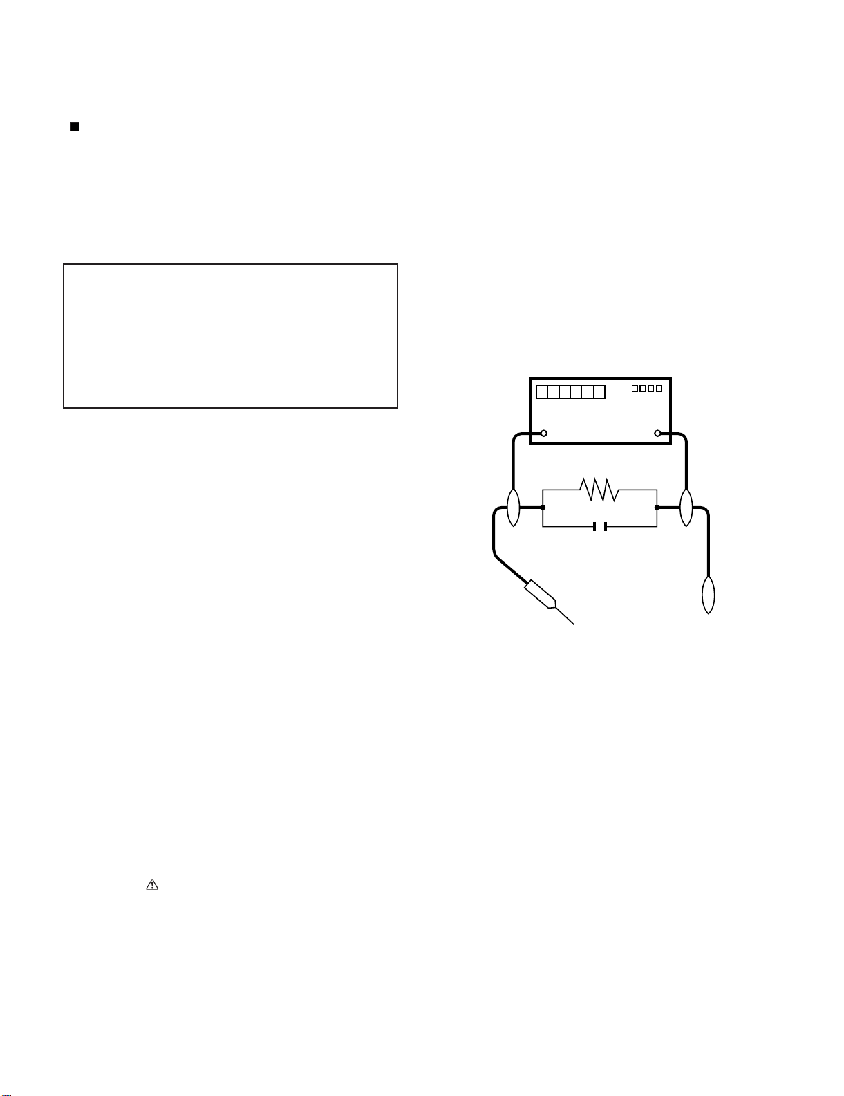
DVM
BEFORE RETURNING THE RECEIVER (Fire &
Shock Hazard)
Before returning the receiver to the user, perform the following
safety checks:
3. Inspect all lead dress to make certain that leads are not pinched,
and check that hardware is not lodged between the chassis and
other metal parts in the receiver.
4. Inspect all protective devices such as non-metallic control knobs,
insulation materials, cabinet backs, adjustment and compartment
covers or shields, isolation resistor-capacitor networks, mechanical
insulators, etc.
5. To be sure that no shock hazard exists, check for leakage current in
the following manner.
• Plug the AC cord directly into a 120 volt AC outlet.
• Using two clip leads, connect a 1.5k ohm, 10 watt resistor paralleled by a 0.15µF capacitor in series with all exposed metal cabinet
parts and a known earth ground, such as electrical conduit or electrical ground connected to an earth ground.
///////////////////////////////////////////////////////////////////////////////////////////////////////////////////////////////////////////////////////////////////////////////////////////////////////////////////////////////////////////
TO EXPOSED
METAL PARTS
AC SCALE
1.5k ohm
10W
0.15µF
TEST PROBE
CONNECT TO
KNOWN EARTH
GROUND
SAFETY NOTICE
Many electrical and mechanical parts in LCD color television have
special safety-related characteristics.
These characteristics are often not evident from visual inspection, nor
can protection afforded by them be necessarily increased by using
replacement components rated for higher voltage, wattage, etc.
Replacement parts which have these special safety characteristics are
identified in this manual; electrical components having such features
are identified by " " and shaded areas in the Replacement Parts List
and Schematic Diagrams.
///////////////////////////////////////////////////////////////////////////////////////////////////////////////////////////////////////////////////////////////////////////////////////////////////////////////////////////////////////////
For continued protection, replacement parts must be identical to those
used in the original circuit.
The use of a substitute replacement parts which do not have the same
safety characteristics as the factory recommended replacement parts
shown in this service manual, may create shock, fire or other hazards.
i
Page 3
LC-32GP1U/LC-37GP1U 1st
PRECAUTIONS A PRENDRE LORS DE LA REPARATION
Ne peut effectuer la réparation qu' un technicien spécialisé qui s'est parfaitement accoutumé à toute vérification de sécurité et aux
conseils suivants.
•
AVERTISSEMENT
1.
N'entreprendre aucune modification de tout circuit. C'est dangereux.
2.
Débrancher le récepteur avant toute réparation.
PRECAUTION: POUR LA PROTECTION CONTINUE CONTRE LES RISQUES D'INCENDIE,
REMPLACER LE FUSIBLE
F701 (250V 8A)
F4702 (250V 4A)
VERIFICATIONS CONTRE L'INCEN-DIE ET LE
CHOC ELECTRIQUE
Avant de rendre le récepteur à l'utilisateur, effectuer les vérifications suivantes.
Inspecter tous les faisceaux de câbles pour s'assurer que les fils
3.
ne soient pas pincés ou qu'un outil ne soit pas placé entre le châssis et les autres pièces métalliques du récepteur.
4.
Inspecter tous les dispositifs de protection comme les boutons de
commande non-métalliques, les isolants, le dos du coffret, les couvercles ou blindages de réglage et de compartiment, les réseaux
de résistancecapacité, les isolateurs mécaniques, etc.
5.
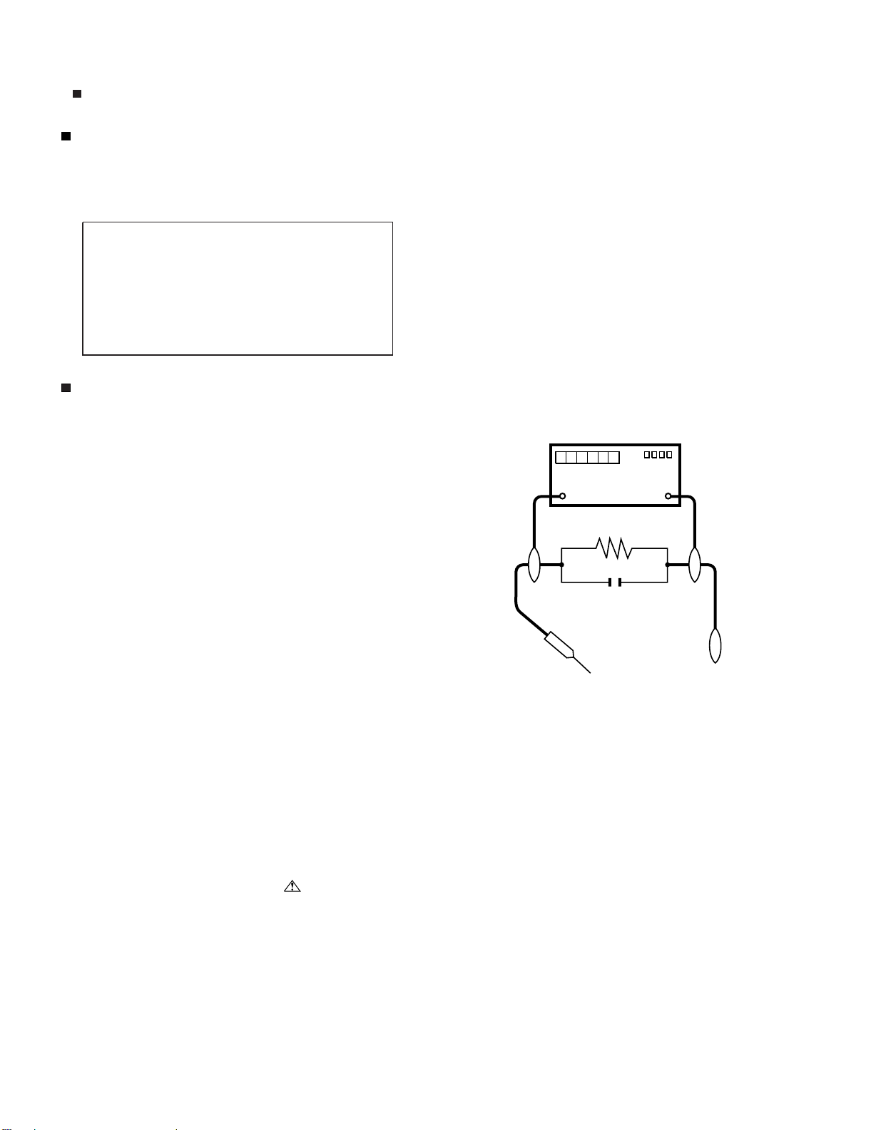
S'assurer qu'il n'y ait pas de danger d'électrocution en vérifiant la
fuite de courant, de la facon suivante:
•
Brancher le cordon d'alimentation directem-ent à une prise de courant de 120V. (Ne pas utiliser de transformateur d'isolation pour
cet essai).
A l'aide de deux fils à pinces, brancher une résistance de 1.5 kΩ
10 watts en parallèle avec un condensateur de 0.15µF en série
avec toutes les pièces métalliques exposées du coffret et une terre
connue comme une conduite électrique ou une prise de terre
branchée à la terre.
•
Utiliser un voltmètre CA d'une sensibilité d'au moins 5000Ω/V pour
mesurer la chute de tension en travers de la résistance.
•
Toucher avec la sonde d'essai les pièces métalliques exposées qui
présentent une voie de retour au châssis (antenne, coffret métallique, tête des vis, arbres de commande et des boutons, écusson,
etc.) et mesurer la chute de tension CA en-travers de la résistance.
Toutes les vérifications doivent être refaites après avoir inversé la
fiche du cordon d'alimentation. (Si nécessaire, une prise
d'adpatation non polarisée peut être utilisée dans le but de terminer ces vérifications.)
La tension de pointe mesurèe ne doit pas dépasser 0.75V (correspondante au courant CA de pointe de 0.5mA).
Dans le cas contraire, il y a une possibilité de choc électrique qui
doit être supprimée avant de rendre le récepteur au client.
DVM
ECHELLE CA
1.5k ohm
10W
µ
F
0.15
SONDE D'ESSAI
AUX PIECES
METALLIQUES
EXPOSEES
/////////////////////////////////////////////////////////////////////////////////////////////////////////////////////////////////////////////////////////////////////////////////////////////////////////////////////////////////////////////
BRANCHER A UNE
TERRE CONNUE
AVIS POUR LA SECURITE
De nombreuses pièces, électriques et mécaniques, dans les téléviseur ACL présentent des caractéristiques spéciales relatives à la sécurité, qui ne sont souvent pas évidentes à vue. Le degré de protection ne peut pas être nécessairement augmentée en utilisant des
pièces de remplacement étalonnées pour haute tension, puissance,
etc.
Les pièces de remplacement qui présentent ces caractéristiques sont
identifiées dans ce manuel; les pièces électriques qui présentent ces
particularités sont identifiées par la marque " " et hachurées dans la
liste des pièces de remplacement et les diagrammes schématiques.
/////////////////////////////////////////////////////////////////////////////////////////////////////////////////////////////////////////////////////////////////////////////////////////////////////////////////////////////////////////////
Pour assurer la protection, ces pièces doivent être identiques à celles
utilisées dans le circuit d'origine. L'utilisation de pièces qui n'ont pas
les mêmes caractéristiques que les pièces recommandées par l'usine,
indiquées dans ce manuel, peut provoquer des électrocutions, incendies, radiations X ou autres accidents.
ii
Page 4
LC-32GP1U/LC-37GP1U 1st
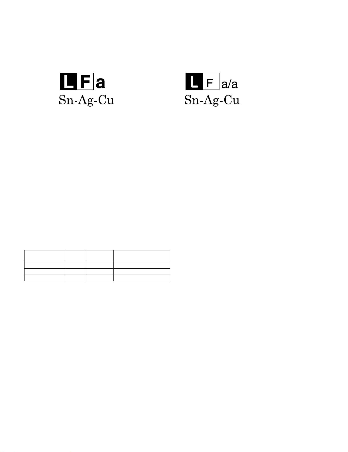
PRECAUTIONS FOR USING LEAD-FREE SOLDER
Employing lead-free solder
• “PWBs” of this model employs lead-free solder. The LF symbol indicates lead-free solder, and is attached on the PWBs and service manuals. The
alphabetical character following LF shows the type of lead-free solder.
Example:
Indicates lead-free solder of tin, silver and copper. Indicates lead-free solder of tin, silver and copper.
Using lead-free wire solder
• When fixing the PWB soldered with the lead-free solder, apply lead-free wire solder. Repairing with conventional lead wire solder may cause damage or accident due to cracks.
As the melting point of lead-free solder (Sn-Ag-Cu) is higher than the lead wire solder by 40 °C, we recommend you to use a dedicated soldering
bit, if you are not familiar with how to obtain lead-free wire solder or soldering bit, contact our service station or service branch in your area.
Soldering
• As the melting point of lead-free solder (Sn-Ag-Cu) is about 220 °C which is higher than the conventional lead solder by 40 °C, and as it has poor
solder wettability, you may be apt to keep the soldering bit in contact with the PWB for extended period of time. However, Since the land may be
peeled off or the maximum heat-resistance temperature of parts may be exceeded, remove the bit from the PWB as soon as you confirm the
steady soldering condition.
Lead-free solder contains more tin, and the end of the soldering bit may be easily corroded. Make sure to turn on and off the power of the bit as
required.
If a different type of solder stays on the tip of the soldering bit, it is alloyed with lead-free solder. Clean the bit after every use of it.
When the tip of the soldering bit is blackened during use, file it with steel wool or fine sandpaper.
• Be careful when replacing parts with polarity indication on the PWB silk.
Lead-free wire solder for servicing
PARTS CODE
ZHNDAi123250E BL J φ0.3mm 250g (1roll)
ZHNDAi126500E BK J φ0.6mm 500g (1roll)
ZHNDAi12801KE BM J φ1.0mm 1kg (1roll)
PRICE
RANK
PART
DELIVERY
DESCRIPTION
iii
Page 5
LC-32GP1U/LC-37GP1U 1st
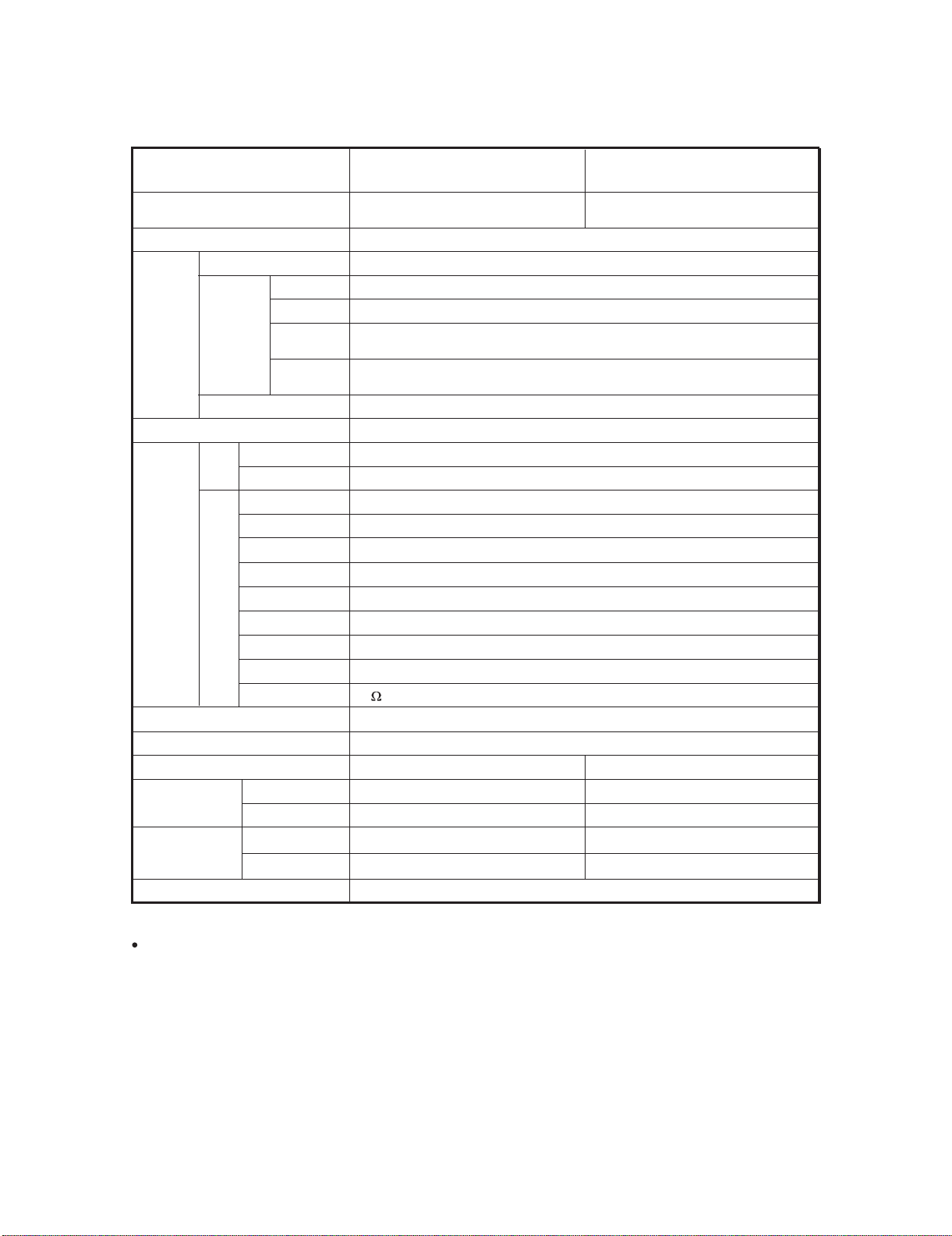
CHAPTER 1. SPECIFICATIONS
[1] SPECIFICATIONS
LC-32GP1U/LC-37GP1U 1st
Service Manual
Item
LCD panel
Number of dots
TV
Function
TV-standard (CCIR)
Receiving
Channel
Audio multiplex
Audio out
Terminals
Side
Rear
VHF/UHF
CATV
Digital Terrestrial
Broadcast (8VSB)
Digital cable
(64/256 QAM)
INPUT 1
INPUT 4
INPUT 2
INPUT 3
INPUT 5
32" Advanced Super View & BLACK TFT
LCD
6,220,800 dots (1920 1080 3 dots)
American TV Standard ATSC/NTSC System
VHF 2-13ch, UHF 14-69ch
1-135ch (non-scrambled channel only)
2-69ch
*1
1-135ch (non-scrambled channel only)
BTSC System
10W 2
AV in, COMPONENT in (Recommend to connect game console)
HDMI in with HDCP (Recommend to connect game console)
S-VIDEO in, AV in
Audio in, COMPONENT in
HDMI in with HDCP
Model: LC-32GP1U
Model: LC-37GP1U
37" Advanced Super View & BLACK TFT
LCD
INPUT 6 Audio in, HDMI in with HDCP
INPUT 7
DIGITAL AUDIO OUTPUT
OUTPUT
SUBWOOFER PRE OUT
ANTENNA 75 Unbalance, F Type 1 for Analog (VHF/UHF/CATV) and Digital (AIR/CABLE)
OSD language
Power Requirement
Power Consumption
Weight
TV + stand
TV only
Dimension
(W H D)
*2
TV + stand
TV only
Operating temperature
*1
Emergency alert messages via Cable are unreceivable.
*2
The dimensional drawings are shown on the inside back cover.
Audio in, DVI-I in with HDCP
Optical Digital audio output 1 (PCM/Dolby Digital)
Audio out
Monaural audio output
English/French/Spanish
AC120V,60Hz
165 W (0.9 W Standby with AC 120V)
44.1 lbs./20.0 kg
36.4 lbs./16.5 kg
25
31
/64239/32103/4inch
25
/642059/64353/64inch
31
32°F to 104°F (0°C to 40°C)
203 W (0.9 W Standby with AC 120V)
52.9 lbs./24.0 kg
44.1 lbs./20.0 kg
3
/16253/4111/2inch
36
3
36
/16235/8353/64inch
As part of policy of continuous improvement, SHARP reserves the right to make design and specification changes for product
improvement without prior notice. The performance specification figures indicated are nominal values of production units.
There may be some deviations from these values in individual units.
1 – 1
Page 6
LC-32GP1U/LC-37GP1U 1st
LC-32GP1U/LC-37GP1U 1st
CHAPTER 2. OPERATION MANUAL
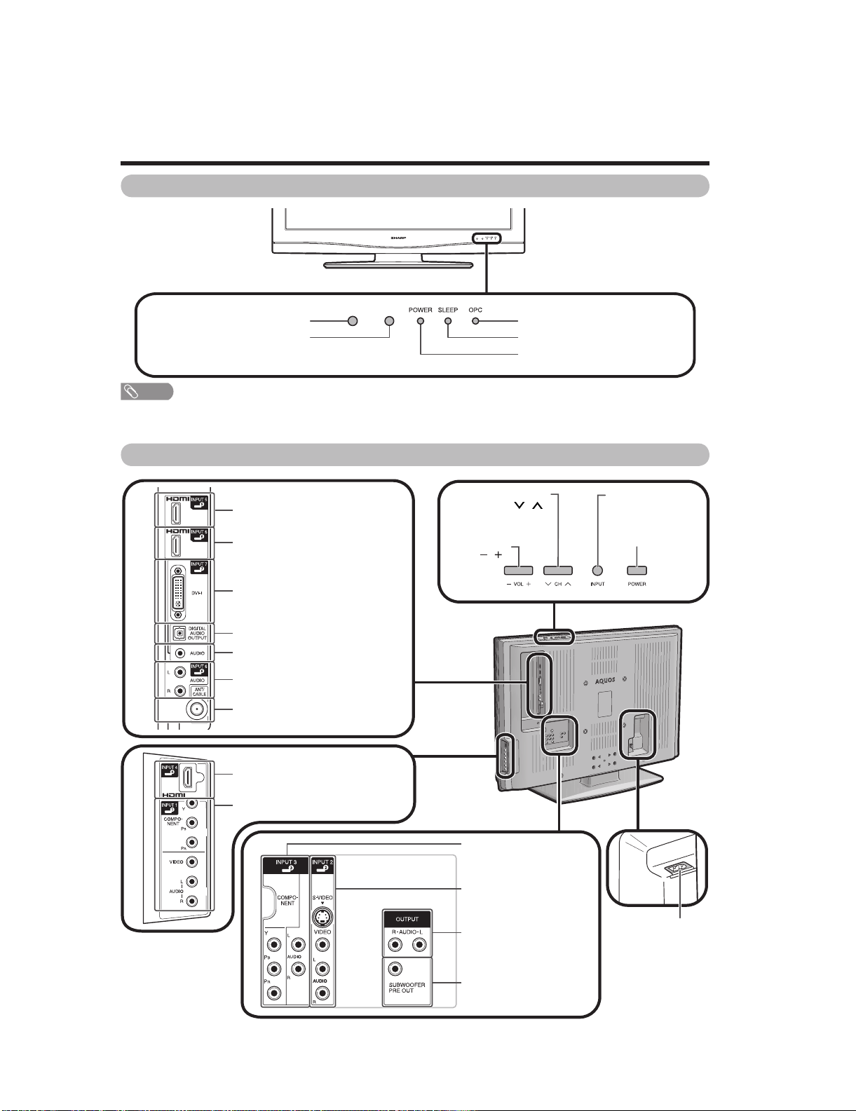
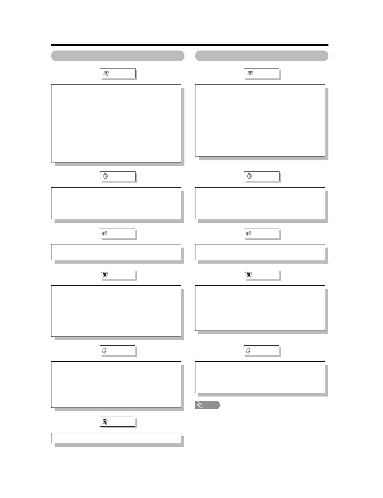
[1] OPERATION MANUAL
Part names
TV (Front)
Service Manual
Remote control sensor
OPC sensor*
NOTE
*OPC: Optical Picture Control
TV (Rear/Side)
HDMI terminal (INPUT 5)
HDMI terminal (INPUT 6)
DVI-I terminal (INPUT 7)
DIGITAL AUDIO OUTPUT terminal
AUDIO terminal (INPUT 7)
AUDIO terminals (INPUT 6)
Antenna/Cable in
Channel buttons
(CH /)
Volume
buttons
(VOL /)
OPC indicator*
SLEEP indicator**
POWER indicator**
INPUT button
POWER button
HDMI terminal (INPUT 4)
INPUT 1 terminals
2 – 1
INPUT 3 terminals
INPUT 2 terminals
AUDIO OUTPUT terminals
SUBWOOFER PRE OUT
AC INPUT terminal
Page 7
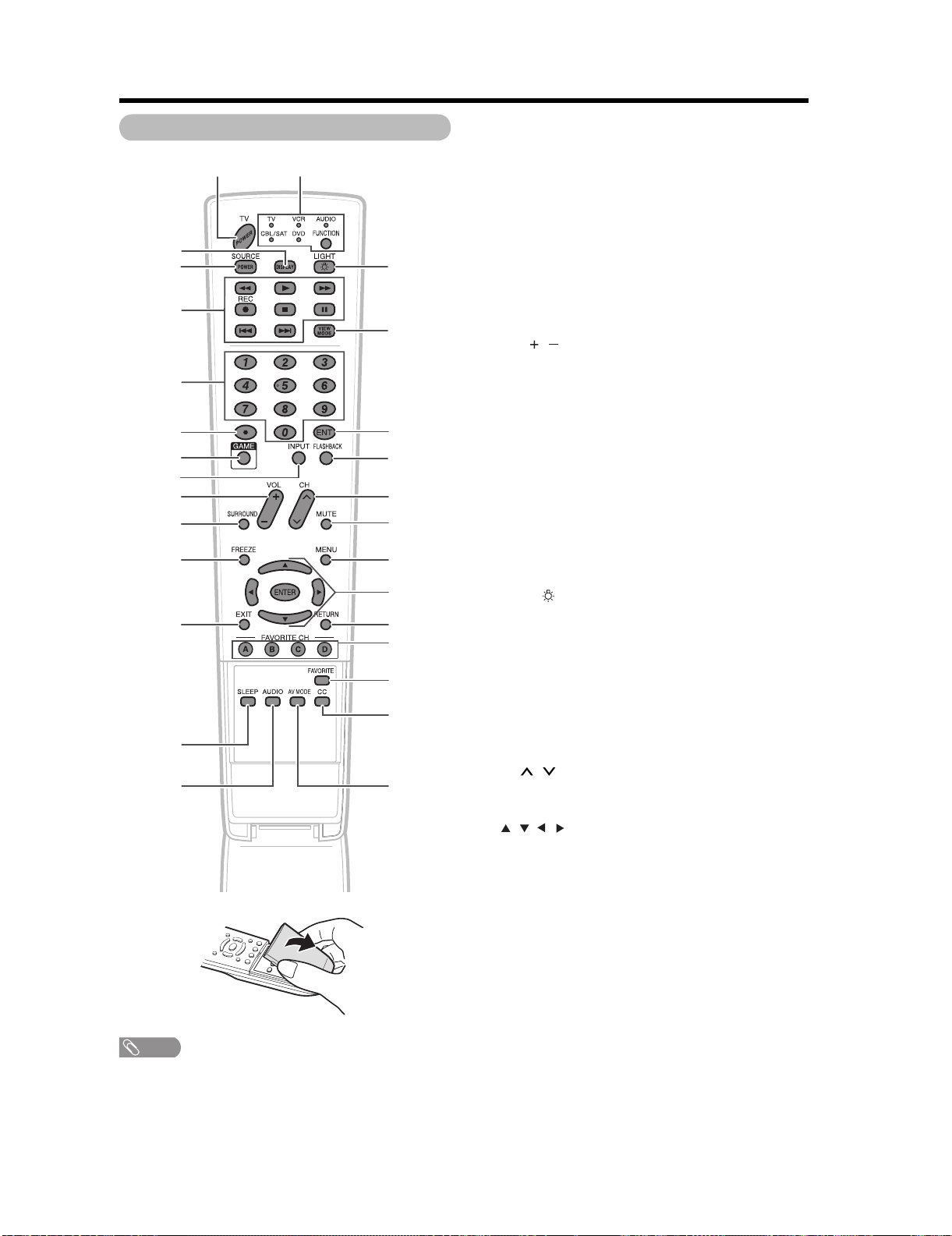
Part names
LC-32GP1U/LC-37GP1U 1st
Remote control unit
115
2
3
4
5
6
7
8
9
10
11
16
17
18
19
20
21
22
1 TV POWER: Switch the TV power on or enters
standby.
2 DISPLAY: Display the channel information.
3 SOURCE POWER: Turns the power of the external
equipment on and off.
4 External equipment operational buttons: Operate
the external equipment.
50_9: Set the channel.
6 (DOT):
•
7GAME:Selects INPUT 1 or INPUT 4.
8 INPUT: Select a TV input source. (TV, INPUT 1,
INPUT 2, INPUT 3, INPUT 4, INPUT 5, INPUT 6,
INPUT 7)
9VOL /:Set the volume.
10 SURROUND: Select Surround settings.
11 FREEZE: Set the still image. Press again to return to
normal screen.
12 EXIT: Turn off the menu screen.
13 SLEEP: Set the sleep timer.
14 AUDIO: Selects the MTS/SAP or the audio mode
during multi-channel audio broadcasts.
15 FUNCTION: Switches the remote control for TV,
CBL/SAT, VCR, DVD and AUDIO operation. Indicator
lights up for the current mode.
* To enter the code registration mode, you need to
press FUNCTION
DISPLAY at the same time.
and
12 24
13
14 28
NOTE
•
When using the remote control unit, point it at the TV.
23
25
26
27
16 LIGHT : When pressed all buttons on the remote
control unit will light. The lighting will turn off if no
operations are performed within about 5 seconds.
This button is used for performing operations in lowlight situations.
17 VIEW MODE: Select the screen size.
18 ENT: Jumps to a channel after selecting with the
buttons.
19 FLASHBACK:Return to the previous channel or
external input mode.
20 CH / : Select the channel.
21 MUTE: Mute the sound.
22 MENU: Display the menu screen.
23 ////ENTER: Select a desired item on the
screen.
24 RETURN: Return to the previous menu screen.
25 FAVORITE CH
A, B, C, D: Select 4 preset favorite channels in 4
different categories.
While watching, you can toggle the selected channels
by pressing A, B, C and D.
26 FAVORITE: Set the favorite channels.
27 CC: Display captions from a closed-caption source.
28 AV MODE: Select an audio or video setting.
(When the input source is TV, INPUT 1, 2 or 3:
STANDARD, MOVIE, GAME, USER, DYNAMIC (Fixed),
DYNAMIC. When the input source is INPUT 4, 5, 6 or
7: STANDARD, MOVIE, GAME, PC, USER, DYNAMIC
(Fixed), DYNAMIC.)
0_9
2 – 2
Page 8
LC-32GP1U/LC-37GP1U 1st
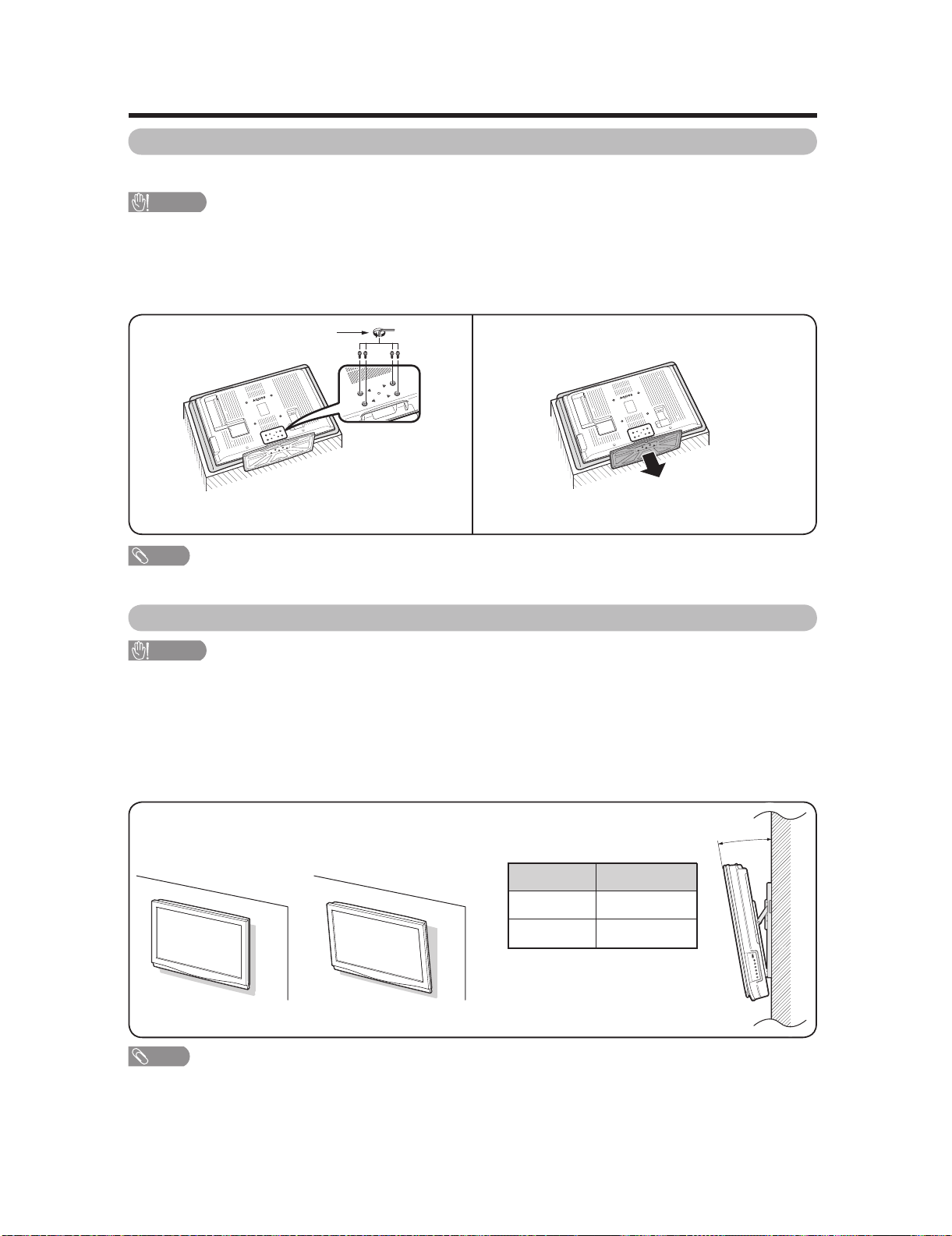
Appendix
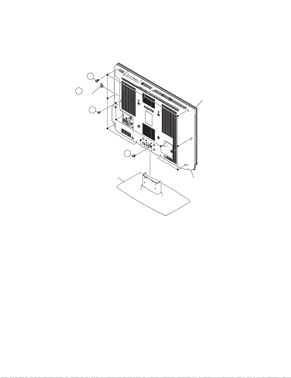
Removing the stand
Before detaching (or attaching) stand, unplug the AC cord from the AC INPUT terminal.
CAUTION
Do not remove the stand from the TV unless using an optional wall mount bracket to mount it.
•
Before attaching/detaching stand
Before performing work make sure to turn off the TV.
•
Before performing work spread cushioning over the base area to lay the TV on. This will prevent it from being
•
damaged.
1
Unfasten the four screws used to secure the stand in
place.
NOTE
To attach the stand, perform the above steps in reverse order.
•
Hex key
2
Detach the stand from the TV. (Hold the stand so it
will not drop from the edge of the base area.)
Setting the TV on the wall
CAUTION
This TV should be mounted on the wall only with the AN-37AG2 (SHARP) wall mount bracket. The use of other wall
•
mount brackets may result in an unstable installation and may cause serious injuries.
Installing the TV requires special skill that should only be performed by qualified service personnel. Customers
•
should not attempt to do the work themselves. SHARP bears no responsibility for improper mounting or mounting
that results in accident or injury.
Using an optional bracket to mount the TV
You can ask a qualified service professional about using an optional AN-37AG2 bracket to mount the TV to the wall.
•
Carefully read the instructions that come with the bracket before beginning work.
•
Hanging on the wall
AN-37AG2 wall mount bracket.
(See the bracket instructions for details.)
LC-32GP1U
LC-37GP1U
Vertical mounting
NOTE
Detach the cable clamps on the rear of the TV when using the optional mount bracket.
•
Due to the terminal configuration on this TV, when you wall-mount this model, make sure there is enough space between the
•
wall and the TV for the cables.
Angular mounting
About setting the TV angle
Model
Angle of TV
0/5/10°
0/5/10°
2 – 3
Page 9
Appendix
Troubleshooting
LC-32GP1U/LC-37GP1U 1st
Problem
power
No
•
•
Unit cannot be operated.
Remote control unit does not
•
operate.
Picture is cut off/with sidebar
•
screen.
•
Strange color, light color, or color
misalignment
Power is suddenly turned off.
•
Possible Solution
Check if you pressed TV POWER on the remote control unit. If the
•
indicator on the TV does not light up, press POWER on the TV.
Is the AC cord disconnected?
•
•
Has the power been turned on?
•
External influences such as lightning, static electricity, may cause improper operation.In this case, operate the unit after first turning on the power of the TV or unplugging
the AC cord and replugging it in after 1 or 2 minutes.
Is the FUNCTION set correctly? Set it to the TV setting position.
•
Are batteries inserted with polarity ( , ) aligned?
•
Are batteries worn out? (Replace with new batteries.)
•
Are you using it under strong or fluorescent lighting? -
•
Is a fluorescent light illuminated near the remote control sensor? -
•
Is the image position correct?
•
Are screen mode adjustments such as picture size made correctly?
•
Adjust the picture tone.
•
Is the room too bright? The picture may look dark in a room that is too bright.
•
Check the input signal setting.
Is the sleep timer set?
•
Check the power control settings.
•
•
The unit's internal temperature has increased. Remove any objects blocking vent or
clean.
No picture
•
No sound
•
Is connection to other components correct?
•
Is correct input signal source selected after connection?
•
Is the correct input selected?
•
Is picture adjustment correct?
•
Is "On" selected in "Audio Only"?
•
Is a non-compatible signal being input?
Is the volume too low?
•
Is "Variable" selected in "Output Select"?
•
Have you pressed MUTE on the remote control unit?
•
Is "On" selected in "Subwoofer"?
•
Troubleshooting-Digital broadcasting
The error message about reception of broadcast
The example of an error message
displayed on a screen
•
Failed to receive broadcast.
No broadcast now.
•
Error code
•
E202
E203 Check the broadcast time in the program guide.
Check the antenna cable. Check that the antenna is correctly
setup.
•
Possible Solution
Cautions regarding use in high and low temperature environments
When the unit is used in a low temperature space (e.g. room, office), the picture may leave trails or appear slightly delayed.
•
This is not a malfunction, and the unit will recover when the temperature returns to normal.
Do not leave the unit in a hot or cold location. Also, do not leave the unit in a location exposed to direct sunlight or near a
•
heater, as this may cause the cabinet to deform and the Liquid Crystal panel to malfunction.
Storage temperature: 4°F to 140°F ( 20°C to 60°C)
2 – 4
Page 10
LC-32GP1U/LC-37GP1U 1st
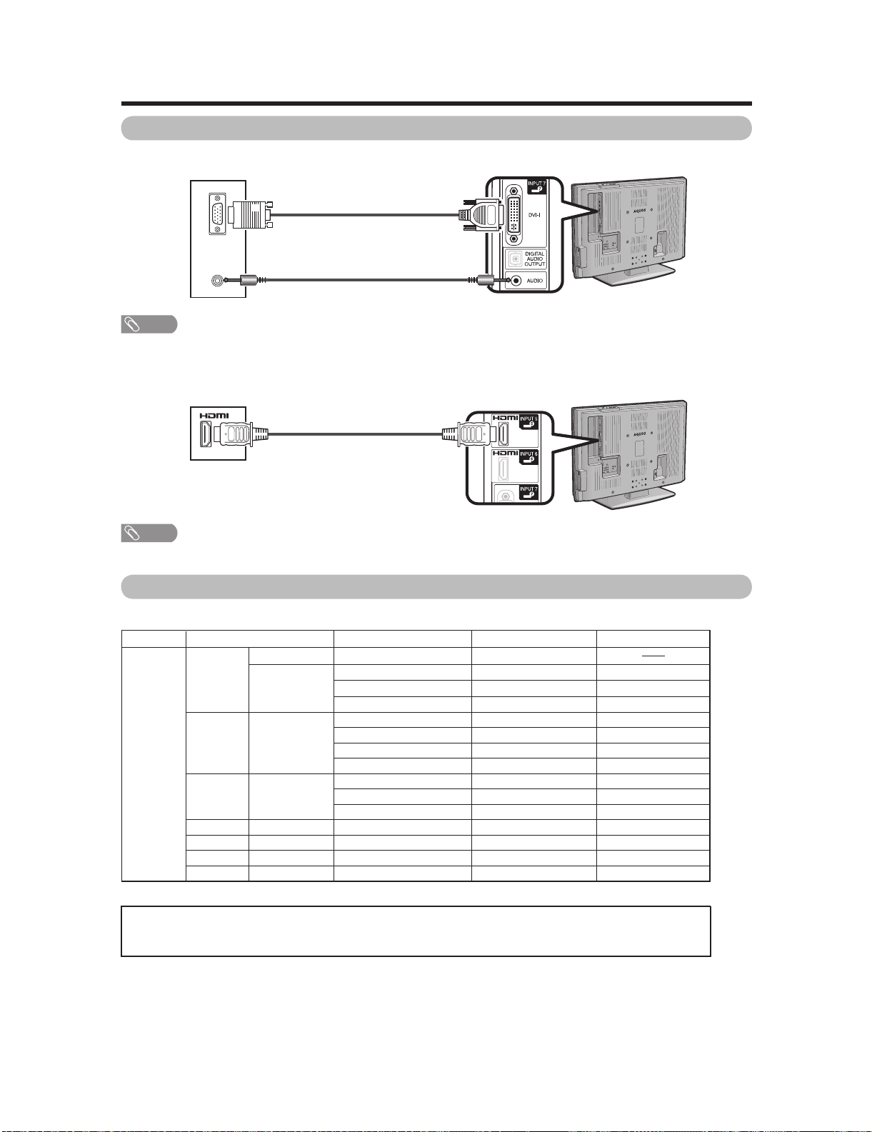
Preparation
Connecting a PC
When connecting to a PC with a DVI terminal. (INPUT 7)
PC
NOTE
If you are connecting the TV to a PC with a DVI terminal, use a DVI cable (commercially available) instead of a RGB/DVI
•
conversion cable.
When connecting to a PC with an HDMI terminal. (INPUT 4, 5 or 6)
RGB/DVI Conversion cable
(commercially available)
Ø 3.5 mm stereo minijack cable
(commercially available)
Example
(commercially available)
PC
NOTE
The HDMI terminals only support digital signal.
•
HDMI cable
PC compatibility chart
It is necessary to set the PC correctly to display XGA and WXGA signal.
PC Resolution Horizontal Frequency Vertical Frequency VESA Standard
70 Hz
60 Hz
72 Hz
75 Hz
56 Hz
60 Hz
72 Hz
75 Hz
60 Hz
70 Hz
75 Hz
60 Hz
60 Hz
60 Hz
60 Hz
PC
*DVI input only.
720 x 400
VGA
XGA 1024 x 768
WXGA 1360 x 768
SXGA
SXGA *
UXGA*
+
640 x 480
800 x 600SVGA
1280 x 1024
1400 x 1050
1600 x 1200
31.5 kHz
31.5 kHz
37.9 kHz
37.5 kHz
35.1 kHz
37.9 kHz
48.1 kHz
46.9 kHz
48.4 kHz
56.5 kHz
60.0 kHz
47.7 kHz
64.0 kHz
64.0 kHz
75.0 kHz
O
O
O
O
O
O
O
O
O
O
O
O
O
O
DDC is a registered trademark of Video Electronics Standards Association.
Power Management is a registered trademark of Sun Microsystems, Inc.
VGA and XGA are registered trademarks of International Business Machines Co., Inc.
2 – 5
Page 11
LC-32GP1U/LC-37GP1U 1st
Basic adjustment settings
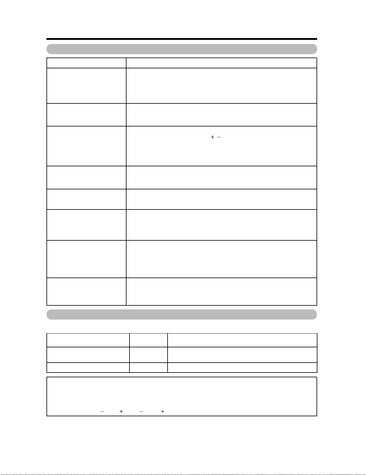
Menu items for TV/INPUT 1/2/3 Menu items for HDMI/DVI
OPC
Backlight
Contrast
Brightness
Color
Tint
Sharpness
Advanced
Color Temp.
Black
3D-Y/C
Monochrome
Film Mode
Range of OPC
Reset
Treble
Bass
Balance
Surround
Subwoofer
Reset
No Signal Off
No Operation Off
Picture
Audio
Power Contr
Picture
OPC
Backlight
Contrast
Brightness
Color
Tint
Sharpness
Advanced
Color Temp.
Black
Monochrome
Film Mode
Range of OPC
Reset
Audio
Treble
Bass
Balance
Surround
Subwoofer
Reset
ol
No Signal Off
No Operation Off
Power Contr
ol
EZ Setup
CH Setup
Antenna Setup-DIGITAL
Input Skip
Input Label
Parental CTRL
Position
Language
Reset
Audio Only
Digital Noise Reduction
Input Select
Output Select
Color System
Caption Setup
Program Title Display
Favorite CH
Audio Setup
Setup
Option
Digital Setup
Setup
Input Skip
Input Signal
Auto Sync.
Input Label
Fine Sync.
Position
Language
Reset
Option
Audio Only
Digital Noise Reduction
Input Select
HDMI Setup
Output Select
NOTE
Some menu items may not be displayed depending on the
•
selected input source.
2 – 6
Page 12
LC-32GP1U/LC-37GP1U 1st
LC-32GP1U/LC-37GP1U 1st
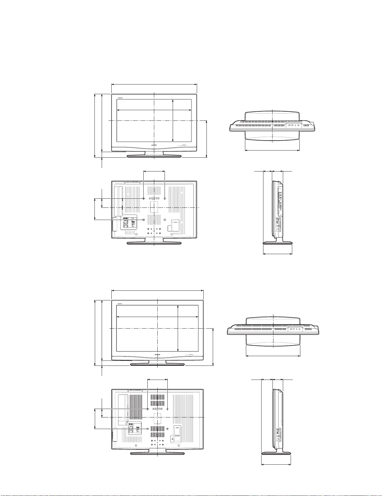
CHAPTER 3. DIMENSIONS
[1] DIMENSIONS
Service Manual
LC-32GP1U
(591)
32
/
9
23
3
23
(200)
8
/
7
7
8
/
2
64
/
3
(531)
64
/
59
20
(60)
(85)
31
275/8(701.4)
25
/64(
797)
77/8(200)
32
/
19
15
(396.1)
(344)
64
/
35
13
3
15
(88)
Unit: Inch/(mm)
31
19
/32(507)
32
/
353/
(97)
64
LC-37GP1U
(654)
4
/
3
25
9
23
(200)
8
/
7
7
64
/
2
64
/
3
(600)
8
/
5
23
(54)
(85)
3225/64(822.6)
3
36
/16(919)
77/8(200)
64
/
17
18
(463.8)
(374)
64
/
47
14
437/
(116)
21
64
103/4(273)
17
/64(540)
3
53
(97)
64
/
3 – 1
11
1
/2(292)
Page 13
LC-32GP1U/LC-37GP1U 1st
CHAPTER 4. REMOVING OF MAJOR PARTS
Service Manual
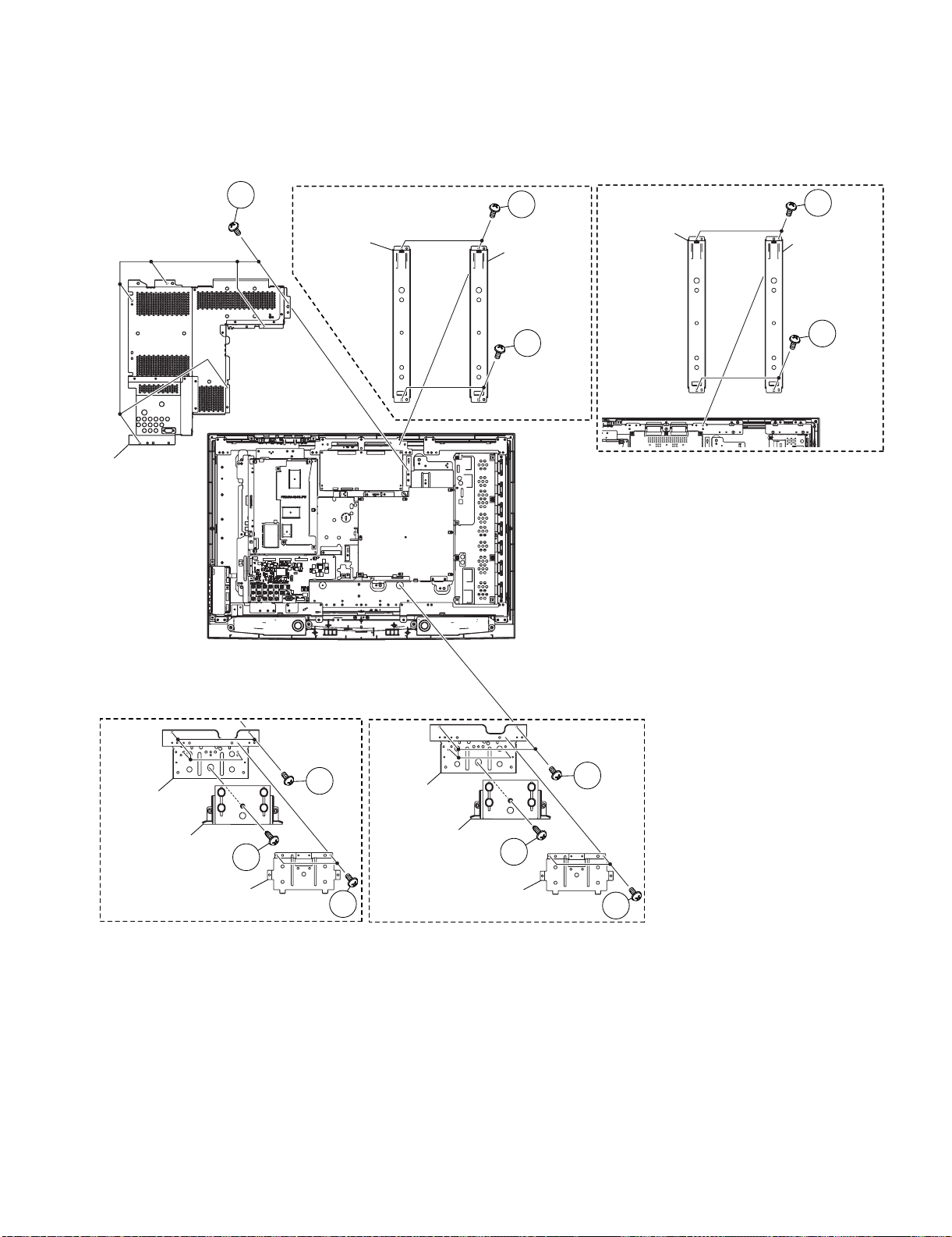
[1] REMOVING OF MAJOR PARTS
1. Remove the SD Card Cover.
2. Remove the 4 lock screws and detach the Stand Base Ass'y.
3. Remove the 9 lock screws, 4 lock screws and detach the Rear Cabinet.
3
1
SD Card Cover
3
LC-32GP1U/LC-37GP1U 1st
Front Cabinet
2
Stand Base Ass'y
Rear Cabinet
4 – 1
Page 14
LC-32GP1U/LC-37GP1U 1st
4. Remove the 2 lock screws and detach the Stand Assist Angle.
5. Remove the 4 lock screws and detach the Center Angle-L and R.
6. Remove the 1 lock screw and detach the Stand Area Cover.
7. Remove the 4 lock screws and detach the Stand Fix Angle.
8. Remove the 6 lock screws and detach the MAIN Shield.
MAIN Shield
8
LC-32GP1U
Center Angle-R
5
Center Angle-L
5
LC-37GP1U
Center Angle-R
5
Center Angle-L
5
Stand Fix Angle
Stand Area Cover
Stand Assist Angle
6
LC-32GP1U
7
4
Stand Fix Angle
Stand Area Cover
Stand Assist Angle
LC-37GP1U
7
6
4
4 – 2
Page 15
LC-32GP1U/LC-37GP1U 1st
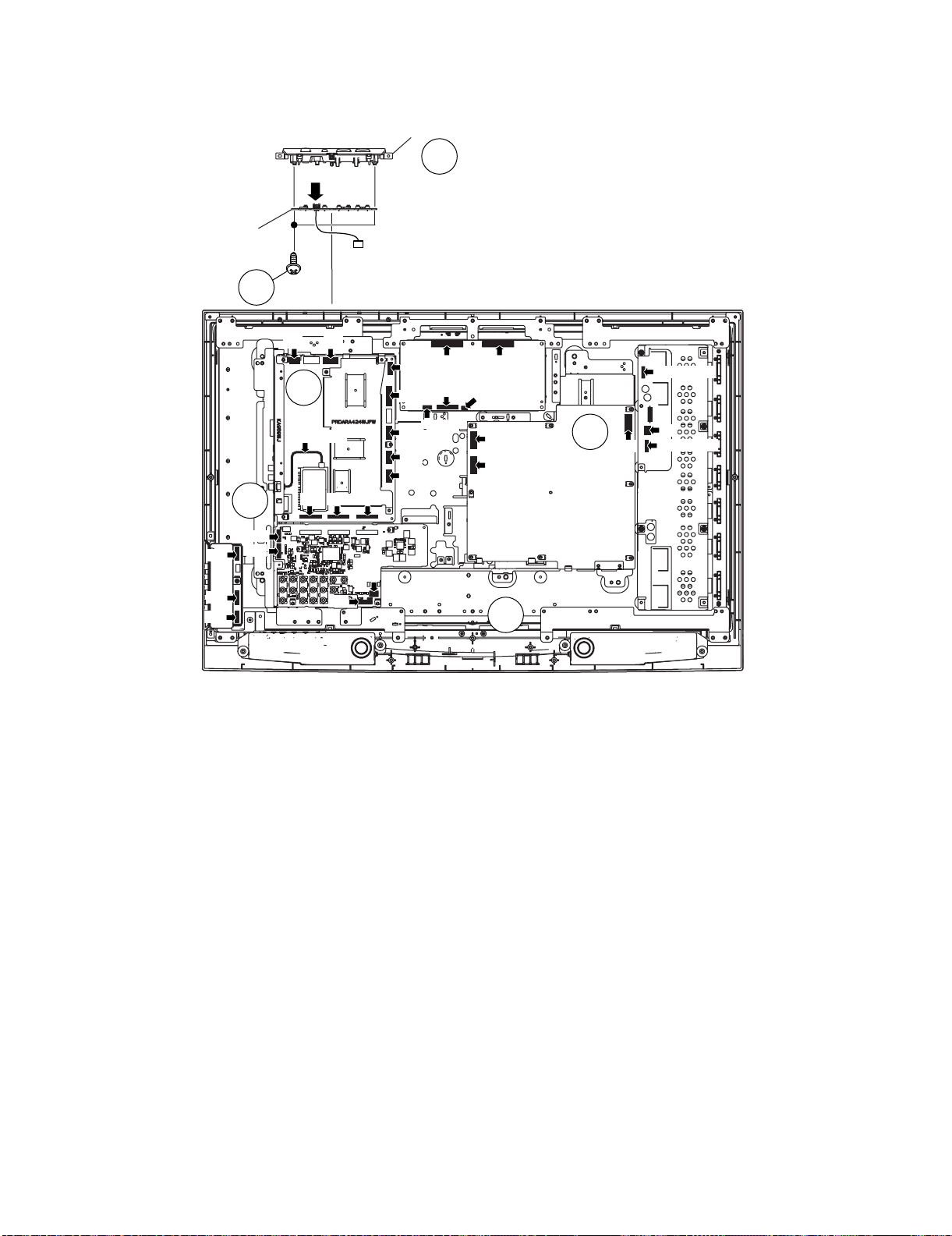
9. Disconnect all the connectors from all the PWBs.
10.Remove the Top Cover Ass'y. Remove the 2 lock screws from the Top Cover Ass'y and detach the KEY Unit.
Top Cover
10
[KM]
KEY Unit
10
[KM]
[GA]
[CN5](32GP1U)
[CN4](37GP1U)
[LP]
9
[F-RCA wire]
9
[MA] [FC]
[SA]
[LV]
[LB]
[PH]
[PD]
[CN1]
[CN2](37GP1U)
[CN4](32GP1U)
[CN3](37GP1U)
[CN2](32GP1U)
[PE]
[PD]
[LB](32GP1U)
[LA]
[LA]
[LB](37GP1U)
9
[HM]
[TS]
[VD]
[VD]
[VE]
[SP]
[RA]
9
4 – 3
Page 16
LC-32GP1U/LC-37GP1U 1st
11.Remove the 4 lock screws and detach the Speaker-L and R.
12.Remove the 1 lock screw and detach the GAME Unit Ass’y.
13.Remove the 4 lock screws from the GAME Unit Ass’y and detach the GAME Unit.
14.Remove the 2 lock screws and detach the R/C, LED Unit.
15.Remove the 5 lock screws and detach the Tray Chassis.
15
LC-37GP1U
GAME Unit Holder
13
13
13
12
GAME Unit
GAME Unit Shield
LC-32GP1U
GAME Unit Holder
13
13
12
GAME Unit
GAME Unit Shield
13
Tray Chassis
11
Speaker-R
R/C, LED Unit
14
Speaker-L
11
4 – 4
Page 17
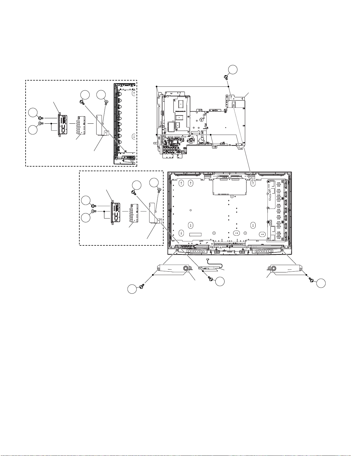
16.Remove the 2 lock screws, 2 lock Shaft and detach the Jack Angle.
17.Remove the 7 lock screws and detach the POWER Unit.
18.Remove the 4 lock screws and detach the TERMINAL Unit.
19.Remove the 5 lock screws, 2 lock rivets and detach the MAIN PWB Radiator and MAIN Unit.
LC-32GP1U/LC-37GP1U 1st
16
16
MAIN PWB Radiator
19
MAIN Unit
19
19
17
POWER Unit
Jack Angle
18
TERMINAL Unit
4 – 5
Page 18
LC-32GP1U/LC-37GP1U 1st
20.Remove the 6 lock screws and detach the Rug Angle Top-L and R. (LC-32GP1U)
Remove the 4 lock screws and detach the Rug Angle Top-L and R. (LC-37GP1U)
21.Remove the 6 lock screws and detach the Rug Angle Bottom-L and R.
22.Remove the 3 lock screws and detach the Chassis Fix Angle Top. (LC-32GP1U)
Remove the 5 lock screws and detach the Chassis Fix Angle Top. (LC-37GP1U)
23.Remove the LCD Panel Module.
LC-32GP1U
20
Rug Angle Top-R
Rug Angle Bottom-R
21
LC-37GP1U
20
21
Chassis Fix Angle Top
20
22
22
Chassis Fix Angle Top
22
22
20
Rug Angle Top-L
21
20
20
Rug Angle Bottom-L
21
Rug Angle Top-R
Rug Angle Bottom-R
21
21
4 – 6
21
Rug Angle Top-L
Rug Angle Bottom-L
21
Page 19
LC-32GP1U/LC-37GP1U 1st
LC-32GP1U/LC-37GP1U 1st
CHAPTER 5. ADJUSTMENT
Service Manual
[1] ADJUSTMENT PROCEDURE
The adjustment values are set to the optimum conditions at the factory before shipping. If a value should become improper or an adjustment is
required due to part replacement, make an adjustment according to the following procedure.
1. After replacement of any PWB unit and/or IC for repair, please note the following.
When replacing the following units, make sure to prepare the new units loaded with updated software.
MAIN Unit: DUNTKE028FM05
2. Upgrading of each microprocessor software
CAUTION: Never “POWER OFF” the unit when software upgrade is ongoing.
Otherwise the system may be damaged beyond recovery.
2.1. Software version upgrade
The model employs the following software.
•Main software
• Monitor microprocessor software
The main software and the monitor microprocessor software can be upgraded by using a general-purpose SD memory card.
The followings are the procedures for upgrading, explained separately for each of the main software, the monitor microprocessor software.
2.2. Main software version upgrade
2.2.1 Get ready before you start
• SD memory card of 32MB or higher capacity
• PC running on Windows 98/98SE/ME/2000/XP operating system
• SD memory card reader/writer with USB connectivity
• SD memory card formatting software
(Downloadable at http://panasonic.jp/support/audio/sd/download/sd_formatter_e.html)
2.2.2 Preparations
To upgrade the main software, it is necessary to get ready the SD card for version upgrade before you start. Follow the steps below and create the SD
card for version upgrade.
1. Insert the SD card into the SD card reader/writer. Start the SD card formatting software. Click [Format]. (When you have the drive options, select
the drive where the SD card is inserted before you proceed.)
5 – 1
Page 20
LC-32GP1U/LC-37GP1U 1st
2. When the formatting is over, the following window appears. Click [OK].
3. Click [Exit] to finish the formatting.
NOTE: When you are done, take out the SD card once to make sure it is finished, and then insert it again.
4. Copy the binary image file GP1UAxxx.SDC (named temporarily) for version upgrade to the root directory (folder) of the SD card drive.
NOTE: In the SD card drive, do not store other folders or unrelated files, or more than one binary image files for version upgrade.
Now the SD card for version upgrade is ready.
2.2.3 Upgrading the software
1. Turn off the AC power (Unplug the AC power cord).
2. Insert the upgrading SD card (prepared as instructed above) into the service slot.
NOTE: Be careful not to insert the SD card in the wrong way. Otherwise the card may come into the set and fail to come out.
3. Turn on the AC power (Plug in the AC power cord).
4. A couple to dozen seconds after the set starts, the upgrade screen below shows up.
5 – 2
Page 21
LC-32GP1U/LC-37GP1U 1st
5. If any of the procedures fails, the following upgrade failure screen shows up. For the failing procedure, the “NG” marking turns red.
NOTE: In such case, try to upgrade the software again. If it still fails, the hardware may be in trouble.
6. When all the procedures are complete, the following upgrade success screen shows up. The new software version can be confirmed on screen.
The version number appears when each item has been successfully upgraded. Finally the main version number appears on screen.
7. Turn off the AC power (Unplug the AC power cord). Take out the upgrading SD card.
8. Now the software has been upgraded.
NOTE: Then get the set started and call the process adjustment screen 1/29 to check the main software version.
CAUTION: 1) Do not take out and put in the SD memory card during formatting.
2) With the SD formatted, all the data stored on the medium will be deleted.
3) Do not start the SD formatting with the memory card's WRITE PROTECT switch still on.
4) If the SD memory card format software does not recognize the SD memory card, take out and put in the SD memory card again, and
click the “UPDATE” button.
5) After checking the performance, use the set under its interface environment.
6) The SD formatting is impossible on drives that are not recognized “REMOVABLE”.
2.3. Upgrading the monitor microprocessor software
2.3.1 Kit
Have the above “Upgrading the main software” kit or equivalent at hand.
2.3.2 Preparations
As discussed in “Upgrading the main software” earlier, create the SD card for upgrading the monitor microprocessor software. For this SD card, use
the monitor microprocessor upgrading binary image file.
2.3.3 Upgrading procedure
To follow the monitor microprocessor software upgrading, the monitor screen upgrade progress indicator and the flashing power LED indicator can be
used.
1. Turn off the AC power (Unplug the AC power cord).
2. Insert the upgrading SD card (prepared as instructed above) into the service slot at the back of the set. Insert the SD card with its logo-printed face
upward (visible). Be careful not to insert the SD card in the wrong way. Otherwise the card may come into the set and fail to come out.
3. Turn on the AC power (Plug in the AC power cord).
CAUTION: Now the monitor microprocessor software starts getting upgraded. Be very careful not to turn off the power while the software is being
upgraded. Otherwise the software will fail to upgrade itself and the set will fail to get started.
5 – 3
Page 22
LC-32GP1U/LC-37GP1U 1st
4. A couple to dozen seconds after the set starts, the upgrade screen below shows up. The upgrade progress is indicated on screen. The power LED
indicator goes out once and then starts flashing in green. (It takes 2-3 minutes to get the monitor microprocessor software upgraded.)
5. If the procedure fails, the following upgrade failure screen shows up and the “NG” marking turns red. The power LED indicator fails to start flashing
in green. Even if the usual screen reappears in several seconds, do the procedure from Step “1” again.
NOTE: In case of failure, try to upgrade the software again. If it still fails, the hardware may be in trouble.
6. When the procedure is complete, the following upgrade success screen shows up. The new software version can be confirmed on screen. The
upgrade success can also be confirmed when the power LED indicator and the OPC LED indicator start flashing alternately in green, respectively.
Double-check the upgrading and turn off the AC power (Unplug the AC power cord). Take out the upgrading SD card. Now the software has been
upgraded.
Finally get the set started and call the process adjustment screen 1/29 to check the monitor microprocessor software version.
5 – 4
Page 23
LC-32GP1U/LC-37GP1U 1st
3. Entering and exiting the adjustment process mode
1) Before entering the adjustment process mode, the AV position RESET in the video adjustment menu.
2) While holding down the “VOL (–)” and “INPUT” keys at a time, plug in the AC cord of the main unit to turn on the power.
The letter “<K>” appears on the screen.
3) Next, hold down the “VOL (–)” and “CH ( )” keys at a time.
(The “VOL (–)” and “CH ( )” keys should be pressed and held until the display appears.)
Multiple lines of blue characters appearing on the display indicate that the unit is now in the adjustment process mode.
When you fail to enter the adjustment process mode (the display is the same as normal startup), retry the procedure.
4) To exit the adjustment process mode after the adjustment is done, unplug the AC cord from the outlet to make a forced shutdown. (When the
power was turned off with the remote controller, once unplug the AC cord and plug it again. In this case, wait 10 seconds or so before plugging.)
CAUTION: Use due care in handling the information described here lest your users should know how to enter the adjustment process mode. If the
4. Remote controller key operation and description of display in adjustment process mode
1) Key operation
Remote controller key Main unit key Function
CH ( / ) CH ( / )
VOL (+/–) VOL (+/–) Changing a selected item setting (+1/ –1)
Cursor (UP/DOWN) ————— Turing a page (PREVIOUS/NEXT)
Cursor (LEFT/RIGHT) ————— Changing a selected line setting (+10/ –10)
INPUT ————— Input switching (toggle switching)
ENTER ————— Executing a function
2) Description of display
settings are tampered in this mode, unrecoverable system damage may result.
Moving an item (line) by one (UP/DOWN)
(TUNER→INPUT1→INPUT2→INPUT3→INPUT4→INPUT5→INPUT6→INPUT7)
*Input mode is switched automatically when relevant adjustment is started so far as the necessary input signal is available.
(1) Current page/ (5) Destination
Total pages
1/29 [INFO] INPUT5 AUTO USA 46_UNDER
MAIN Version 0.90 ( U 2006/11/21 1A)
BOOT Version GP1UB 1.01
Monitor Version 0.9
EQ DATACHECKSUM ROM (8) Parameters
TEMPAERATURE 7B
LAMP ERROR 0
NORMAL STANDBY CAUSE
ERROR STANDBY CAUSE 1) 0 2) 0 3) 0
(2) Current page title
(3) Current selected input
(4) Current color system
0
0H 0M 0H 0M 0H 0M
4) 0 5) 0
0H 0M 0H 0M
(6) LCD Panel size/Speaker type
(LC-32GP1U: 32_UNDER)
(LC-37GP1U: 37_UNDER)
(7) Adjustment
process menu
header
5 – 5
Page 24
LC-32GP1U/LC-37GP1U 1st
5. List of adjustment process mode menu
The character string in brackets [ ] will appear as a page title in the adjustment process menu header.
Page Line Item Description Remarks (adjustment detail, etc.)
1 [INFO]
1 MAIN Version Main software version
2BOOT Version
3 Monitor Version Monitor software version
4 EQ DATA CHECKSUM Audio data checksum
5 TEMPERATURE CPU temperature
6 LAMP ERROR Number of termination due to lamp error
7 NORMAL STANDBY CAUSE Refer to *1 under the list for details
8 ERROR STANDBY CAUSE Refer to *2 under the list for details
2 [INIT]
1 INDUSTRY INIT (Cause)
2 INDUSTRY INIT Initialization to factory settings .
3 HOTELMODE Hotel mode
4 Center Acutime Accumulated main operation time
5 RESET Reset
6 BacklightAcutime Accumulated monitor operation time
7 RESET Reset
8 LAMP ERROR RESET Reset LAMP ERROR
9 VIC XPOS X-coordinate setting for VIC READ
10 VIC YPOS Y-coordinate setting for VIC READ
11 VIC COLOR Collected color data setting for VIC READ
12 VIC SIGNAL TYPE Signal type setting for VIC READ
13 VIC READ Picture level acquisition function Level appears in green on the upper right.
3 [N358MAIN]
1 N358 ALL ADJ CVBS and TUNER signal level adjustment
2 N358 MAIN ADJ CVBS signal level adjustment
3 TUNER DAC ADJ TUNER signal level adjustment
4 N358 MAIN CONTRAST CVBS and TUNER contrast adjustment values
5 TUNER A DAC TUNER adjustment value
6 VCOM ADJ VCOM adjustment value
4 [TUNER TEST]
1 TUNER VCHIP TEST(69ch) Tuning test and VCHIP test (69 ch)
2 TUNER VCHIP TEST(7ch) Tuning test and VCHIP test (7 ch)
3 TUNER VCHIP TEST(10ch) Tuning test and VCHIP test (10 ch)
4 TUNER VCHIP TEST(15ch) Tuning test and VCHIP test (15 ch)
5 [COMP15KMAIN]
1 COMP15K MAIN ADJ Component 15K picture level adjustment (main)
2 COMP15K CONTRAST Contrast adjustment value
3 COMP15K MAIN Cb GAIN Cb GAIN adjustment value
4 COMP15K MAIN Cr GAIN Cr GAIN adjustment value
5 COMP15K Y OFFSET Y OFFSET adjustment value
6 COMP15K Cb OFFSET Cb OFFSET adjustment value
7 COMP15K Cr OFFSET Cr OFFSET adjustment value
6 [HDTV]
1 HDTV ADJ Component Hi-Vision picture level adjustment
2 CONTRAST Contrast adjustment value
3 Cb GAIN Cb GAIN adjustment value
4 Cr GAIN Cr GAIN adjustment value
5 HDTV Y OFFSET Y OFFSET adjustment value
6 HDTV Cb OFFSET Cb OFFSET adjustment value
7 HDTV Cr OFFSET Cr OFFSET adjustment value
7 [COMP67K]
1 COMP67K ADJ (33K)
2 COMP67K ADJ (67K)
3 COMP67K CONTRAST
4 COMP67K Cb GAIN
5 COMP67K Cr GAIN
6 COMP67K Y OFFSET
7 COMP67K Cb OFFSET
8 COMP67K Cr OFFSET
5 – 6
Page 25
LC-32GP1U/LC-37GP1U 1st
Page Line Item Description Remarks (adjustment detail, etc.)
8 [DVI ANALOG]
1 DVI ANALOG ADJ
2 R CUTOFF
3G CUTOFF
4 B CUTOFF
5 R DRIVE
6 G DRIVE
7 B DRIVE
9 [FR DDRTEST]
1 DDRA TEST1
2 DDRA TEST2
3 DDRB TEST1
4 DDRB TEST2
5 DDRB TEST3
10 [M GAMMA IN]
1 MONITOR GAMMA IN 1 Standard value 1(WBI10184) Adjustment gradation setting.
2 MONITOR GAMMA IN 2 Standard value 2(WBI20352)
3 MONITOR GAMMA IN 3 Standard value 3(WBI30528)
4 MONITOR GAMMA IN 4 Standard value 4(WBI40656)
5 MONITOR GAMMA IN 5 Standard value 5(WBI50800)
6 MONITOR GAMMA IN 6 Standard value 6(WBI60928)
7 GAMMA WRITE WB adjustment data writing
8 GAMMA RESET WB adjustment data reading
11 [M GAMMA R1]
1 MONITOR GAMMA R 1 WB adjustment Point 1, R adjustment value Parameter for six-point adjustment
2 MONITOR GAMMA G 1 WB adjustment Point 1, G adjustment value
3 MONITOR GAMMA B 1 WB adjustment Point 1, B adjustment value
4 MONITOR GAMMA R 2 WB adjustment Point 2, R adjustment value
5 MONITOR GAMMA G 2 WB adjustment Point 2, G adjustment value
6 MONITOR GAMMA B 2 WB adjustment Point 2, B adjustment value
7 MONITOR GAMMA R 3 WB adjustment Point 3, R adjustment value
8 MONITOR GAMMA G 3 WB adjustment Point 3, G adjustment value
9 MONITOR GAMMA B 3 WB adjustment Point 3, B adjustment value
10 GAMMA WRITE WB adjustment data writing
11 GAMMA RESET WB adjustment data reading
12 [M GAMMA R4]
1 MONITOR GAMMA R 4 WB adjustment Point 4, R adjustment value Parameter for six-point adjustment
2 MONITOR GAMMA G 4 WB adjustment Point 4, G adjustment value
3 MONITOR GAMMA B 4 WB adjustment Point 4, B adjustment value
4 MONITOR GAMMA R 5 WB adjustment Point 5, R adjustment value
5 MONITOR GAMMA G 5 WB adjustment Point 5, G adjustment value
6 MONITOR GAMMA B 5 WB adjustment Point 5, B adjustment value
7 MONITOR GAMMA R 6 WB adjustment Point 6, R adjustment value
8 MONITOR GAMMA G 6 WB adjustment Point 6, G adjustment value
9 MONITOR GAMMA B 6 WB adjustment Point 6, B adjustment value
10 GAMMA WRITE WB adjustment data writing
11 GAMMA RESET WB adjustment data reading
13 [SOUND 1]
1 AUDIO SWITCH
2 FORCED FLAT MODE
3 AIN1_ADC_VOLUME
4 AIN2_ADC_VOLUME
5 AIN3_ADC_VOLUME
6 AIN4_ADC_VOLUME
7 AIN5_ADC_VOLUME
8 AIN6_ADC_VOLUME
5 – 7
Page 26
LC-32GP1U/LC-37GP1U 1st
Page Line Item Description Remarks (adjustment detail, etc.)
14 [SOUND 2]
1 INPUT_MIXER_GAIN_SP
2 INPUT_MIXER_GAIN_HP
3 INPUT_MIXER_GAIN_EXT
4 INPUT_MIXER_GAIN_EXT_HP
5 OUTPUT_MIXER_GAIN
6SUB_VOLUME_FLAT
7 SUB_VOLUME_EQ
8 SUB_VOLUME_AUDYSSEY
15 [SOUND 3]
1 PEQ1_F0
2 PEQ1_Q
3 PEQ1_GAIN
4 PEQ2_F0
5 PEQ2_Q
6 PEQ2_GAIN
7 PEQ3_F0
8 PEQ3_Q
9 PEQ3_GAIN
10 PEQ4_F0
11 PEQ4_Q
12 PEQ4_GAIN
16 [SOUND 4]
1 PEQ5_F0
2 PEQ5_Q
3 PEQ5_GAIN
4 VIRTUALIZER_LEVEL
5 BASS_BOOST_LEVEL
6 SLICER_LEVEL
7HPF_SW
8 HPF_LR
9LPF_SW
10 SW_MIXING_LEVEL
17 [M OPC1]
1 BRIGHTNESS DA0
2 BRIGHTNESS DA1
3 BRIGHTNESS DA2
4 BRIGHTNESS DA3
5 BRIGHTNESS DA4
6 BRIGHTNESS DA5
7 BRIGHTNESS DA6
8 BRIGHTNESS DA7
9 BRIGHTNESS DA8
10 BRIGHTNESS DA9
11 BRIGHTNESS DA10
12 BRIGHTNESS DA11
18 [M OPC2]
1 BRIGHTNESS DA12
2 BRIGHTNESS DA13
3 BRIGHTNESS DA14
4 BRIGHTNESS DA15
5 BRIGHTNESS DA16
6 BRIGHTNESS DA17
7 BRIGHTNESS DA18
8 BRIGHTNESS DA19
9 BRIGHTNESS DA20
10 BRIGHTNESS DA21
11 BRIGHTNESS DA22
5 – 8
Page 27
LC-32GP1U/LC-37GP1U 1st
Page Line Item Description Remarks (adjustment detail, etc.)
19 [M OPC3]
1 BRIGHTNESS DA23
2 BRIGHTNESS DA24
3 BRIGHTNESS DA25
4 BRIGHTNESS DA26
5 BRIGHTNESS DA27
6 BRIGHTNESS DA28
7 BRIGHTNESS DA29
8 BRIGHTNESS DA30
9 BRIGHTNESS DA31
10 BRIGHTNESS DA32
20 [M ADL1]
1 OPC33 ADLEVEL 0
2 OPC33 ADLEVEL 1
3 OPC33 ADLEVEL 2
4 OPC33 ADLEVEL 3
5 OPC33 ADLEVEL 4
6 OPC33 ADLEVEL 5
7 OPC33 ADLEVEL 6
8 OPC33 ADLEVEL 7
9 OPC33 ADLEVEL 8
10 OPC33 ADLEVEL 9
11 OPC33 ADLEVEL 10
12 OPC33 ADLEVEL 11
21 [M ADL2]
1 OPC33 ADLEVEL 12
2 OPC33 ADLEVEL 13
3 OPC33 ADLEVEL 14
4 OPC33 ADLEVEL 15
5 OPC33 ADLEVEL 16
6 OPC33 ADLEVEL 17
7 OPC33 ADLEVEL 18
8 OPC33 ADLEVEL 19
9 OPC33 ADLEVEL 20
10 OPC33 ADLEVEL 21
11 OPC33 ADLEVEL 22
22 [M ADL3]
1 OPC33 ADLEVEL 23
2 OPC33 ADLEVEL 24
3 OPC33 ADLEVEL 25
4 OPC33 ADLEVEL 26
5 OPC33 ADLEVEL 27
6 OPC33 ADLEVEL 28
7 OPC33 ADLEVEL 29
8 OPC33 ADLEVEL 30
9 OPC33 ADLEVEL 31
23 [M V6THE]
1V6 OS THERMO 1
2V6 OS THERMO 2
3V6 OS THERMO 3
4V6 OS THERMO 4
5V6 OS THERMO 5
6V6 OS THERMO 6
7V6 OS THERMO 7
24 [M V5THE]
1V5 OS THERMO 1
2V5 OS THERMO 2
3V5 OS THERMO 3
4V5 OS THERMO 4
5V5 OS THERMO 5
6V5 OS THERMO 6
7V5 OS THERMO 7
5 – 9
Page 28
LC-32GP1U/LC-37GP1U 1st
Page Line Item Description Remarks (adjustment detail, etc.)
25 [M EEP SET]
1 MONITOR TIME OUT
2 MONITOR MAX TEMP
3 MONITOR STANDBY CAUSE
26 [M TESTPTRN]
1 LCD TEST PATTERN
27 [FR REGI]
1 READ/WRITE
2 SLAVE ADDRESS
3 REGISTOR ADDRESS
4WRITE DATA
5 READ DATA
28 [MEMORY CLR]
1 KEY LOCK(1217)
2 KOUTEI AREA ALL CLEAR
3 A MODE AREA CLEAR
4 BACKUP AREA CLEAR
5 B MODE AREA CLEAR
6EXECUTION
29 [ETC]
1 EEP SAVE Writing setting values to EEPROM.
2 EEP RECOVER Reading setting values from EEPROM.
3 STANDBY CAUSE RESET Reset stand by cause.
*1 Details of P1.7(NORMAL STANDBY CAUSE)
6 No operation off in the cause of “no operation off”
7 No signal off in the cause of “no signal off”
8 PC power management mode 1 in the cause of “Standby mode MODE1”
9 PC power management mode 2 in the cause of “Standby mode MODE2”
A Off timer in the cause of “SLEEP timer”
C Command from RS232C in the cause of command by RS-232C
*2 Details of P1.8(ERROR STANDBY CAUSE)
5 Prolonged unspecified-signal input in PC mode in the cause of continuous “out of range”, PC input mode
13 Temperature error in the cause of abnormal temperature
16 Monitor trouble detected in the cause of abnormal monitor mode
17 Fan lock in the cause of fan lock
6. Special features
* STANDBY CAUSE (Page 1/29)
Display of a cause (code) of the last standby
The cause of the last standby is recorded in EEPROM whenever possible.
Checking this code will be useful in finding a problem when you repair the troubled set.
* EEP SAVE (Page 29/29)
Storage of EEP adjustment value
* EEP RECOVER (Page 29/29)
Retrieval of EEP adjustment value from storage area
5 – 10
Page 29
LC-32GP1U/LC-37GP1U 1st
7. Video signal adjustment procedure
7.1. Signal adjustment
1. Checking the Device
Before starting the adjustment, make sure the adjustment tool and signal generator are set for Sharp LCD US.
Checking the signal generator level adjustment (Set to the standard level.)
• Composite signal : 0.714 Vp-p ± 0.02 Vp-p (from pedestal to white)
• 15K component signal : Y level : 0.714 Vp-p ± 0.02 Vp-p (from pedestal to white)
PB, PR level : 0.7 Vp-p ± 0.02 Vp-p
• 33K component signal : Y level : 0.7 Vp-p ± 0.02 Vp-p (from pedestal to white)
PB, PR level : 0.7 Vp-p ± 0.02 Vp-p
• 1080P component signal : Y level : 0.7 Vp-p ± 0.02 Vp-p (from pedestal to white)
PB, PR level : 0.7 Vp-p ± 0.02 Vp-p
• DVI-I (Analog RGB) signal : RGB level : 0.7 Vp-p ± 0.02 Vp-p (from pedestal to white)
2. Process mode
Adjustment item Adjustment conditions Adjustment procedure
1 Process mode Enter the process adjustment mode using the process adjustment remote controller.
3. Composite N358 signal/tuner adjustment
Adjustment item Adjustment conditions Adjustment procedure
1 Setting N358 signal
US-10ch
Feed the N358 color bar signal (75% color saturation) to VIDEO 1 input.
Feed the RF signal (by use of US-10ch) to TUNER.
[Video input signal] [US-10ch]
75% Color saturation
100% white 0% black 100% white
2 Automatic adjust-
ment execution
4. Component 15K signal adjustment
Adjustment item Adjustment conditions Adjustment procedure
1 Setting 480i signal Feed the 100% color bar signal to VIDEO 1 COMPONENT input.
Move the cursor to [ N358 ALL ADJ] and press the [ENTER] key.
When [ N358 ALL ADJ FINISH] appears, the adjustment is complete.
100% Color saturation
480i
100% color bar
2 Automatic adjust-
ment execution
100% white
Move the cursor to [ COMP 15K ALL ADJ] and press the [ENTER] key.
When [ COMP 15K ALL ADJ FINISH] appears, the adjustment is complete.
0% black
5 – 11
Page 30
LC-32GP1U/LC-37GP1U 1st
5. Component 33K signal adjustment
Adjustment item Adjustment conditions Adjustment procedure
1 Setting 1080i signal Feed the 100% color bar signal to VIDEO 1 COMPONENT input.
100% Color saturation
100% white
2 Automatic adjust-
ment execution
6. Component 1080P signal adjustment
Adjustment item Adjustment conditions Adjustment procedure
1 Setting 1080p signal Feed the 100% color bar signal to VIDEO 1 COMPONENT input.
Move the cursor to [ HDTV ADJ] and press the [ENTER] key.
When [ HDTV ADJ FINISH] appears, the adjustment is complete.
100% Color saturation
100% white
1080i
100% color bar
0% black
1080p
100% color bar
0% black
2 Automatic adjust-
ment execution
7. DVI-I (analog) signal adjustment
Adjustment item Adjustment conditions Adjustment procedure
1 Setting DVI-I (analog)
signal: XGA
(1024 x 768) 60Hz
SYNC: HV separate
2 Automatic adjust-
ment execution
Move the cursor to [ HDTV ADJ] and press the [ENTER] key.
When [ HDTV ADJ FINISH] appears, the adjustment is complete.
Feed the XGA (100%) white 1/2 window to DVI-I (analog).
1/4
1/2
1/4
1/4
Bring the cursor on [ DVI ANALOG ADJ] and press [ENTER].
[ DVI ANALOG ADJ FINISH] appears when finished.
1/2
100% White
0% Black
1/4
5 – 12
Page 31

LC-32GP1U/LC-37GP1U 1st
7.2. White balance adjustment
1. White balance adjustment
Adjustment item Adjustment conditions Adjustment procedure
1 Setting For detailed adjustment procedure, refer to “Kameyama Model Integral Monitor WB
Adjustment Specifications V1.6”.
1) Make the following settings for the set.
AV MODE: [DYNAMIC]
Backlight: +16
Active Backlight: OFF
Aging time: Min. 60 minutes
2) Connect the white balance adjustment tool to the set.
2 Automatic adjust-
ment execution
[Command]
Process mode
KRSW0001
KKT10037
Setting
KYOF0000
OSDS0001
SBSL0016
Multi-point adjustment
mode
MSET0001
Adjustment value initialization
MSET0004
Point 6
WBI60928
MG6G****
MG6B****
MG6R****
Point 5
WBI50800
MG5G****
MG5B****
MG5R****
[Adjustment procedure]
1) Using the remote controller, transmit the “monitor adjustment process” code.
2) Set the 6th point to the specified gradation level. With the strongest color being fixed,
turn down the R, G and B settings to their reference levels.
3) Set the 5th point to the specified gradation level. Correct the G setting (800 x 6thpoint G setting / 928) (rounded off), and make the R and B settings to their reference
levels.
4) Set the 4th point to the specified gradation level. Correct the G setting (656 x 6thpoint G setting / 928) (rounded off), and make the R and B settings to their reference
levels.
5) Set the 3rd point to the specified gradation level. Correct the G setting (528 x 6thpoint G setting / 928) (rounded off), and make the R and B settings to their reference
levels.
6) Set the 2nd point to the specified gradation level. Correct the G setting (352 x 6thpoint G setting / 928) (rounded off), and make the R and B settings to their reference
levels.
7) Set the 1st point to the specified gradation level. Correct the G setting (184 x 6thpoint G setting / 928) (rounded off), and make the R and B settings to their reference
levels.
8) With the MSET0003 command, write the adjustment values and turn off the AC
power.
* Initial R, G and B settings at point 6: Gradation level set at 928
* Initial R, G and B settings at points 1 thru 5: Corrected G setting at each point
(This is because the adjustment is made to achieve the same remainder of RGB setting /
4 at each point.)
[Adjustment value]
•As per the “standard set” submitted by Engineering Department
“LC-32GP1U/LC-37GP1U” Teaching set
[Adjustment reference] Instrument: Minolta CA-210 Engineering instrument
Point 4 Level Reference Adj. spec Ins. spec
WBI40656 Point 6 928 X=0.272 ±0.0025 ±0.003
MG4G**** y=0.277
MG4B**** Point 5 800 X=0.272 ±0.0025 ±0.003
MG4R**** y=0.277
Point 4 656 X=0.272 ±0.0025 ±0.003
Point 3 y=0.277
WBI30528 Point 3 528 X=0.272 ±0.0035 ±0.005
MG3G**** y=0.277
MG3B**** Point 2 352 X=0.272 ±0.0060 ±0.010
MG3R**** y=0.277
Point 1 184 X=0.272 ±0.0100 ±0.015
y=0.277
Point 2
WBI20352
MG2G****
MG2B****
MG2R****
Point 1
WBI10184
MG1G****
MG1B****
MG1R****
Writing
MSET0003
Note Set conditions for inspection
AV MODE: [DYNAMIC] (Reset)
Monochro: ON
Active Backlight: OFF
Aging Time: Min. 60 minutes
5 – 13
Page 32

LC-32GP1U/LC-37GP1U 1st
7.3. Adjusting procedure by use of [RS-232C]
1. Get ready the PC with COM port (RS-232C) running on Windows 95/98/ME/2000/XP operating system, as well as the RS-232C cross cable.
2. Start the unit with the RS-232C cable connected.
3. Start the terminal software. (The freeware readily available on the Internet will do.)
4. Make the following settings.
Baud rate 9,600 bps
Data LENGTH 8 bit
Parity bit None
Stop bit 1 bit
Flow control None
5. If the settings are correct, the terminal software indicates “ERR” against pressing of the “ENTER” key.
6. After the settings are done correctly, it is possible to make an adjustment by typing in the command shown in the table below and pressing the
“ENTER” key on the keyboard.
7. Command entry is successful if the terminal software indicates “OK” when the “ENTER” is pressed. If “ERR” is shown, retry to enter the command.
8. Send the process mode switching command to switch from the RS232C operation mode to the process mode.
KRSW0001: “ERR” is returned.
KKT10037: When “OK” is returned, the process mode becomes active. When “ERR”, start over from KRSW0001.
9. Send each adjustment command.
7.4. Key writing
1. EDID writing (Main PWB: QPWBXE028WJZZ)
Adjustment item Adjustment conditions Adjustment procedure
1 DVI EDID writing File version checking 1) Using the checker, write the EDID data for DVI to IC1505 that is mounted on the
main PWB.
TL1514: I2C clock, TL1515: I2C data
TL1516: 5V, TL1517: GND
TL1536: write protection (H: WP, Low: write enable)
2 HDMI EDID writing Inspection mode
File version checking
1) Using the checker, write the analog HDMI EDID data to IC801/IC1501/IC1502 that
are mounted on the main PWB.
TL833/1508/1510: I2C clock, TL834/1509/1511: I2C data
TL831/1512/1513: 5V, TL835/1519/1518: GND
TL832/1534/1535: write protection (H: WP, Low: write enable)
2) Write the data before the HDMI inspection with the checker.
(If the EDID has not been written, the HDMI does not function normally.)
7.5. Factory settings
After making the factory settings, pull off the AC cord.
NOTE: Do not turn on the power once the factory settings have been made. Otherwise the factory settings must be made again.
Adjustment item Adjustment conditions Adjustment procedure
1 Factory settings Finally pull off the AC cord. • Move the cursor to the [INDUSTRY INIT (+Cause)] line. Using the [VOL+/–] keys,
set this item ON and press the [ENT] key.
The version confirm window appears on the green screen. When [SUCCESS]
appears at the top, the factory settings are complete. (If an error occurs. [ERROR]
appears on the red screen.)
• Finally turn off the AC power.
The following settings are returned to the factory ones.
1) User settings
2) Channel data (broadcast frequencies, etc.)
3) Password setting
4) Operation time
5) Standby Cause
6) EZ SETUP flag
7) V-CHIP block setting
7.6. Software version
Change of software version is notified at a technical report.
* Main microprocessor
* Monitor microprocessor
* EDID data (DVI, HDMI)
5 – 14
Page 33

LC-32GP1U/LC-37GP1U 1st
CHAPTER 6. TROUBLE SHOOTING TABLE
Service Manual
[1] TROUBLE SHOOTING TABLE
No video (1)
LC-32GP1U/LC-37GP1U 1st
COMPOSITE: No external input video
[INPUT-1]
Is INPUT-1 selected on the
input select menu screen? Is
the INPUT-SELECT for the
input signal?
YES YES
Is there the COMPOSITE
video signal input at pin (71)
of IC501 (AV_SWITCH)?
YES YES
Is there the COMPOSITE video signal output at pin (60) of IC501? NO Check IC501 and its periph-
Is there the COMPOSITE video signal output at pin (2) of connector (SC501) on the TERMINAL unit? NO Check the line between
NO Select INPUT-1 on the input
select menu screen for the
right input signal.
Does the INPUT-1 V2.PLUG
detection function?
Check the line between pin
(6) of input terminal (J801)
and pin (76) of IC501
(AV_SWITCH).
NO Check the line between pin
(7) of J508 and pin (71) of
IC501.
YES
Is INPUT-2 selected on the
input select menu screen?
Is there the COMPOSITE
video signal input at pin (3)
of IC501 (AV_SWITCH)?
COMPOSITE: No external input video
[INPUT-2]
NO Select INPUT-2 on the input
select menu screen.
Does the INPUT-2 V3.PLUG
detection function?
Check the line between pin
(6) of input terminal (J509)
and pin (2) of IC501
(AV_SWITCH).
NO Check the line between pin
(7) of J509 and pin (3) of
IC501.
eral circuits.
IC501 and SC501 (Q501
thru Q504, etc.).
YES
Is there the COMPOSITE video signal input at pin (2) of connector (SC1101) on the MAIN unit? NO Check the SC501 and
YES
Is there the COMPOSITE video signal input at pins (M4, N4) of IC3301 (VPC)? NO Check the line between
YES
Is there the LVDS signal output at the LVDS 1st channel and 2nd channel of IC3301?
TA2_P/M (AJ30/AK30), TB2_P/M (AJ29/AK29), TC2_P/M (AJ28/AK28), TD2_P/M (AJ26/AK26), TE2_P/
M (AJ25/AK25), TCLK2_P/M (AJ27/AK27), TA1_P/M (AB29/AB30), TB1_P/M (AC29/AC30), TC1_P/M
(AD29/AD30), TD1_P/M (AF29/AF30), TE1_P/M (AG29/AG30), TCLK1_P/M (AE29/AE30)
YES
Check the panel module.
SC1101 connectors.
SC1101 and IC3301 (Q2201
thru Q2203, Q2205, Q2207,
Q2209, etc.).
NO Check IC3301 and its
peripheral control circuits
(IC3501, IC3502, IC8101,
etc.).
6 – 1
Page 34

LC-32GP1U/LC-37GP1U 1st
No video (2)
COMPONENT: No external input video
[INPUT-1]
Is INPUT-1 selected on the input select
menu screen? Is the INPUT-SELECT for the
input signal?
NO
Select INPUT-1 on the input
select menu screen for the right
input signal.
Does the INPUT-1 C2.PLUG
detection function?
Check the line between pin (6)
of input terminal (J802) and pin
(40) of IC501 (AV_SWITCH).
YES
Is there the COMPONENT video signal
input at pins (27) (Y) / (29) (Pb) and (31) (Pr)
of IC501 (AV_SWITCH)?
NO
Check the line between the
input terminals of J502 and
IC501.
YES
Is there the COMPONENT video signal output at pins (60) (Y) / (59) (Pb) and (58) (Pr) of
IC501?
COMPONENT: No external input video
[INPUT-3]
Is INPUT-3 selected on the input select
menu screen? Is the INPUT-SELECT for the
input signal?
NO
Select INPUT-3 on the input
select menu screen for the right
input signal.
Does the INPUT-3 C1.PLUG
detection function?
Check the line between pin (6)
of input terminal (J507) and pin
(38) of IC501 (AV_SWITCH).
YES
Is there the COMPONENT video signal input
at pins (21) (Y) / (23) (Pb) and (25) (Pr) of
IC501 (AV_SWITCH)?
NO
Check the line between the
input terminals of J507 and
IC501.
YES
S-VIDEO: No external input video
[INPUT-2]
Is INPUT-2 selected on the input select menu
screen?
NO
Does the INPUT-2 S3.PLUG
detection function?
Check the line between pin (6)
of input terminal (J503) and pin
(42) of IC501 (AV_SWITCH).
YES
Is there the S-VIDEO signal input at pins (5)
(Y) and (7) (C) of IC501 (AV_SWITCH)?
NO
Check the line between pins (3)
(Y) / (4) (C) of J503 and pins (5)
/ (7) of IC501.
NO
Check IC501 and its peripheral
YES
[COMPOSITE signal input] Is there the COMPONENT video signal output at pins (2), (4) and (6) of connector (SC501) on the TERMINAL unit?
[S-VIDEO signal input] Is there the video signal output at pins (2) (Y) and (4) (C) of connector (SC501) on the TERMINAL unit?
YES
[COMPOSITE signal input] Is there the COMPONENT video signal input at pins (2), (4) and (6) of
connector (SC1101) on the MAIN unit?
[S-VIDEO signal input] Is there the video signal input at pins (2) (Y) and (4) (C) of connector
(SC1101) on the MAIN unit?
YES
[COMPOSITE signal input] Is there the COMPONENT video signal input at pins (U3) (Y) / (AA1)
(Pb) and (W3) (Pr) of IC3301 (VPC)?
[S-VIDEO signal input] Is there the video signal input at pins (M4, N4) (Y) and (T1) (C) of IC3301
(VPC)?
YES
Is there the LVDS signal output at the LVDS 1st channel and 2nd channel of IC3301?
TA2_P/M (AJ30/AK30), TB2_P/M (AJ29/AK29), TC2_P/M (AJ28/AK28), TD2_P/M (AJ26/AK26),
TE2_P/M (AJ25/AK25), TCLK2_P/M (AJ27/AK27), TA1_P/M (AB29/AB30), TB1_P/M (AC29/
AC30), TC1_P/M (AD29/AD30), TD1_P/M (AF29/AF30), TE1_P/M (AG29/AG30), TCLK1_P/M
(AE29/AE30)
circuits.
YES
NO
Check the line between IC501
and SC501 (Q501 thru Q504,
etc.).
NO Check the SC501 and SC1101
connectors.
NO Check the line between SC1101
and IC3301 and its peripheral
circuits.
NO Check the line between SC1101
and IC3301 (Q2201 thru
Q2203, Q2205, Q2207. Q2209,
etc.).
NO Check IC3301 and its periph-
eral control circuits (IC3501,
IC3502, IC8101, etc.).
Check the panel module.
YES
6 – 2
Page 35

No video at UHF/VHF broadcast signal reception No video at digital broadcast signal reception
Is the specified TV signal selected on the input select menu screen?
LC-32GP1U/LC-37GP1U 1st
No video (3)
Is there the analog video
signal output at the output
pin (13) of tuner (TU1101)?
YES YES
Is there the video signal output at pin (5) of IC1103
(LEVEL_ADJ)?
YES
Is there the CVBS3 signal
input at pin (N3) of IC3301
(VPC)?
NO Check the tuner, IC8601
(DE-MODULATOR) and
their peripheral circuits
(TUN_SDA/SCL, Q8601).
NO Does the level adjustment
control signal come from pin
(6) of IC1103 to pin (1) of
IC1104?
NO
Check IC1104 and its
peripheral circuits. Replace
as required.
NO Check the line between
IC1103 and IC3301 (Q2204,
Q2208, etc.).
Is there the video signal output at the output pins (20)
and (21) of tuner (TU1101)?
Are there the MPEG signal
outputs (US_TS_PKTSYNC,
US_TS_EN, US_TS_DATA,
US_TS_CLK) from IC8601?
YES
Are there the MPEG signal
inputs (US_TS_PKTSYNC,
US_TS_EN, US_TS_DATA,
US_TS_CLK) at IC8101
(CPU/DECODER)?
YES
Are there the MVY [7:0],
MVC [7:0] and MVCLKO/
MNSYNCO/MVSYNCO sig-
nal outputs from IC8101?
NO Check the tuner, IC8601
(DE-MODULATOR) and
their peripheral circuits
(TUN_SDA/SCL, Q8601).
NO Check IC8601 and its
peripheral control circuits.
NO Check the line between
IC8601 and IC8101.
NO Check IC8101 and its
peripheral circuits.
YES
Are there the MVY [7:0],
MVC [7:0] and MVCLKO/
MNSYNCO/MVSYNCO sig-
nal inputs at IC3301?
YES
Is there the LVDS signal output at the LVDS 1st channel and 2nd channel of IC3301?
TA2_P/M (AJ30/AK30), TB2_P/M (AJ29/AK29), TC2_P/M (AJ28/AK28), TD2_P/M (AJ26/AK26), TE2_P/M (AJ25/AK25), TCLK2_P/M (AJ27/
AK27), TA1_P/M (AB29/AB30), TB1_P/M (AC29/AC30), TC1_P/M (AD29/AD30), TD1_P/M (AF29/AF30), TE1_P/M (AG29/AG30), TCLK1_P/M
(AE29/AE30)
YES NO
Check the panel module. Check IC3301 and its peripheral control circuits (IC3501, IC3502,
IC8101, etc.).
YES
NO Check the line between
IC8101 and IC3301.
6 – 3
Page 36

LC-32GP1U/LC-37GP1U 1st
[HDMI/DVI signal input] No video (4)
No external input video [INPUT-4] No external input video [INPUT-5]
Is INPUT-4 selected on the input select menu screen? Is INPUT-5 selected on the input select menu screen?
NO
Select INPUT-4 on the input select menu screen for the
right input signal.
NO
Does the HOT PLUG detection function? Does the HOT PLUG detection function?
Does the HDMI_HPG5 signal come from pin (18) of con-
nector (SC801) to pin (67) of IC9101 (CPLD)?
Select INPUT-5 on the input select menu screen for the
right input signal.
Does the HDMI_HPG3 signal come from pin (18) of connector (SC1501) to pin (66) of IC9101 (CPLD)?
NO
NO
NO
Check the line between SC801 and IC9101
(CPLD) (Q1704, Q1706, etc.).
YES
Does the HDMI_PLG_ENA signal come from pin (82) of
IC9101 to pin (34) of IC1510 (HDMI/HDCP/DVI COMPLIANT RECEIVER) and pin (40) of IC1702 (DVI/HDMI
SWITCH)?
NO
Check the line between IC9101 and IC1702/
IC1510.
YES
Does the HDP2 signal come from pin (62) of IC1702 to
pin (19) of SC1701?
YES
NO
Check the line between IC1702 and SC1701. Check the line between IC1507 and SC1501.
Does the signal come from connector (SC1701) to the input pins (67
and 68) (CLK±), (70 and 71) (D0±), (73 and 74) (D1±), and (76 and
77) (D2±), all of IC1702?
NO
Is IC1701 (EEPROM) accessed by I2C, with HDMI connected, to read the DDC_I2C CLOCK/DATA data?
NO
Check the DDC line and its peripheral circuits (IC1701
(EEPROM) and its peripherals).
YES
Does the signal come from pins (34 and 35) (CLK±), (31 and 32)
(D0±), (28 and 29) (D1±), and (25 and 26) (D2±) of IC1702 to pins (39
and 40), (43 and 44), (47 and 48), and (51 and 52) of IC1510?
NO
YES
Are there the U3VINY [7:0], U3VINR [7:0], U3VINPBPR [7:0], U3VDIN, U3HDIN,
U3DEIN and U3VINCLK signal outputs from IC1510?
Check IC1702, IC1510 and their peripheral circuits. Check IC1507, IC1510 and their peripheral circuits.
Does the signal come from connector (SC1501) to the input pins (48
and 49) (CLK±), (51 and 52) (D0±), (54 and 55) (D1±), and (57 and 58)
(D2±), all of IC1507?
Does the signal come from pins (34 and 35) (CLK±), (31 and 32) (D0±
(28 and 29) (D1±), and (25 and 26) (D2±) of IC1507 to pins (58 and 59),
(62 and 63), (66 and 67), and (70 and 71) of IC1510?
NO
Check the line between SC1501 and IC9101
(CPLD) (Q1506, Q1508, etc.).
YES
Does the HDMI_PLG_ENB signal come from pin (81) of
IC9101 to pin (33) of IC1510 (HDMI/HDCP/DVI COMPLIANT RECEIVER) and pin (40) of IC1507 (DVI/HDMI
SWITCH)?
NO
Check the line between IC9101 and IC1507/
IC1510.
YES
Does the HDP3 signal come from pin (44) of IC1507 to pin
(19) of SC1501?
YES
NO
NO
Is IC1501 (EEPROM) accessed by I2C, with HDMI connected, to read the DDC_I2C CLOCK/DATA data?
NO
Check the DDC line and its peripheral circuits (IC1501
(EEPROM) and its peripherals).
YES
NO
YES
NO Check IC1510 and its peripheral circuits.
),
YES
Are there the U3VINY [7:0], U3VINR [7:0], U3VINPBPR [7:0], U3VDIN, U3HDIN,
U3DEIN and U3VINCLK signal inputs at IC3301 (VPC)?
YES
Is there the LVDS signal output at the LVDS 1st channel and 2nd channel of IC3301?
TA2_P/M (AJ30/AK30), TB2_P/M (AJ29/AK29), TC2_P/M (AJ28/AK28), TD2_P/M
(AJ26/AK26), TE2_P/M (AJ25/AK25), TCLK2_P/M (AJ27/AK27), TA1_P/M (AB29/
AB30), TB1_P/M (AC29/AC30), TC1_P/M (AD29/AD30), TD1_P/M (AF29/AF30),
TE1_P/M (AG29/AG30), TCLK1_P/M (AE29/AE30)
YES
Check the panel module.
6 – 4
NO Check the line between IC1510 and IC3301.
NO Check IC3301 and its peripheral control circuits
(IC3501, IC3502, IC8101, etc.).
Page 37

LC-32GP1U/LC-37GP1U 1st
[HDMI/DVI signal input] No video (4)
No external input video [INPUT-6] No external input video [INPUT-7]
Is INPUT-6 selected on the input select menu screen? Is INPUT-7 selected on the input select menu screen?
NO
Select INPUT-6 on the input select menu screen for the
right input signal.
NO
Does the HOT PLUG detection function? Does the HOT PLUG detection function?
Does the HDMI_HPG2 signal come from pin (18) of connector (SC1502) to pin (61) of IC9101 (CPLD)?
NO
Check the line between SC1502 and IC9101
(CPLD) (Q1505, Q1507, etc.).
YES
Does the HDMI_PLG_ENB signal come from pin (81) of
IC9101 to pin (33) of IC1510 (HDMI/HDCP/DVI COMPLIANT RECEIVER) and pin (40) of IC1507 (DVI/HDMI
SWITCH)?
NO
Check the line between IC9101 and IC1507/
IC1510.
YES
Does the HDP2 signal come from pin (62) of IC1507 to pin
(19) of SC1502?
YES
NO NO
Check the line between IC1507 and SC1502. Check the line between IC1507 and SC1503.
Select INPUT-7 on the input select menu screen for the
right input signal.
Does the HDMI_HPG1 signal come from pin (14) of connector (SC1503) to pin (58) of IC9101 (CPLD)?
Check the line between SC1503 and IC9101
(CPLD) (Q1501, Q1502, etc.).
YES
Does the HDMI_PLG_ENB signal come from pin (81) of
IC9101 to pin (33) of IC1510 (HDMI/HDCP/DVI COMPLIANT RECEIVER) and pin (40) of IC1507 (DVI/HDMI
SWITCH)?
Check the line between IC9101 and IC1507/
IC1510.
YES
Does the HDP1 signal come from pin (44) of IC1507 to
pin (19) of SC1503?
YES
NO
NO
NO
NO
Does the signal come from connector (SC1502) to the input pins (67
and 68) (CLK±), (70 and 71) (D0±), (73 and 74) (D1±), and (76 and 77)
(D2±), all of IC1507?
NO
Is IC1502 (EEPROM) accessed by I2C, with HDMI connected, to read the DDC_I2C CLOCK/DATA data?
NO
Check the DDC line and its peripheral circuits (IC1502
(EEPROM) and its peripherals).
YES
Does the signal come from pins (34 and 35) (CLK±), (31 and 32) (D0±), (28 and 29)
(D1±), and (25 and 26) (D2±) of IC1507 to pins (57 and 58), (62 and 63), (66 and 67),
and (70 and 71) of IC1510?
YES
Are there the U3VINY [7:0], U3VINR [7:0], U3VINPBPR [7:0], U3VDIN, U3HDIN,
U3DEIN and U3VINCLK signal outputs from IC1510?
YES
Are there the U3VINY [7:0], U3VINR [7:0], U3VINPBPR [7:0], U3VDIN, U3HDIN,
U3DEIN and U3VINCLK signal inputs at IC3301 (VPC)?
YES
Is there the LVDS signal output at the LVDS 1st channel and 2nd channel of IC3301?
TA2_P/M (AJ30/AK30), TB2_P/M (AJ29/AK29), TC2_P/M (AJ28/AK28), TD2_P/M
(AJ26/AK26), TE2_P/M (AJ25/AK25), TCLK2_P/M (AJ27/AK27), TA1_P/M (AB29/
AB30), TB1_P/M (AC29/AC30), TC1_P/M (AD29/AD30), TD1_P/M (AF29/AF30),
TE1_P/M (AG29/AG30), TCLK1_P/M (AE29/AE30)
YES
Check the panel module.
Does the signal come from connector (SC1503) to the input pins (5
and 6) (CLK±), (8 and 9) (D0±), (11 and 12) (D1±), and (14 and 15)
(D2±), all of IC1507?
YES
NO
Is IC1503 (EEPROM) accessed by I2C, with HDMI connected, to read the DDC_I2C CLOCK/DATA data?
NO
Check the DDC line and its peripheral circuits (IC1505
(EEPROM) and its peripherals).
NO Check IC1507, IC1510 and their peripheral
circuits.
NO Check IC1510 and its peripheral circuits.
NO Check the line between IC1510 and IC3301.
NO Check IC3301 and its peripheral control cir-
cuits (IC3501, IC3502, IC8101, etc.).
6 – 5
Page 38

LC-32GP1U/LC-37GP1U 1st
No audio (1)
[Audio signal] INPUT-1 No audio [Audio signal] INPUT-2 No audio [Audio signal] INPUT-3 No audio
[INPUT-1 input]
Is INPUT-1 selected on the input select menu
screen?
NO
Is the audio output selected for
“VARIABLE” on the menu
screen?
YES YES YES
Set the audio output to “FIXED”. Set the audio output to “FIXED”. Set the audio output to
YES
[INPUT-1] Does the audio signal come from
pins (5) (L) and (4) (R) of input terminal (J801)
to pins (11) (L) and (9) (R) of connector
(P801) on the GAME unit?
NO
Check the audio signal from J801
to P801, and their peripheral circuits.
YES
[INPUT-1] Is there the audio signal input at
pins (11) (L) and (9) (R) of connector (P501)
on the TERMINAL unit?
[INPUT-2 input]
Is INPUT-2 selected on the input select menu
screen?
NO
Is the audio output selected for
“VARIABLE” on the menu
screen?
YES
[INPUT-2] Does the audio signal come from
pins (4) (L) and (2) (R) of input terminal (J509)
to pins (12) (L) and (10) (R) of connector
(SC502) on the TERMINAL unit?
NO
Check the audio signal from J509
to SC502, and their peripheral circuits.
[INPUT-3 input]
Is INPUT-3 selected on the input select
menu screen?
NO
Is the audio output selected
for “VARIABLE” on the menu
screen?
YES
“FIXED”.
[INPUT-3] Does the audio signal come
from pins (4) (L) and (2) (R) of input terminal (J505) to pins (4) (L) and (2) (R) of connector (SC502) on the TERMINAL unit?
NO
Check the audio signal from
J505 to SC502, and their
peripheral circuits.
NO
Check the P501 and P801 connectors.
YES
[INPUT-1] Does the audio signal come from
pins (8) (L) and (6) (R) of TERMINAL unit?
NO
Check the audio signal from P501
to SC502, and their peripheral cir-
cuits.
YES
[INPUT-1] Is there the audio signal input at
pins (8) (L) and (6) (R) of connector (SC1102)
on the MAIN unit?
NO
Check the SC502 and SC1102
connectors.
YES
[INPUT-1] Does the audio signal come from
pins (8) and (6) of SC1102 to pins (59) (L) and
(60) (R) of IC1404 (CODEC)?
NO
Check the line between SC1102
and IC1404 and their peripheral
circuits.
YES
Is there the audio signal output at pins (38) (L) and (39) (R) of IC1404?
YES
[INPUT-2] Is there the audio signal input at
pins (12) (L) and (10) (R) of connector
(SC1102) on the MAIN unit?
Check the SC502 and SC1102
connectors.
YES
[INPUT-2] Does the audio signal come from
pins (12) and (10) of SC1102 to pins (53) (L)
and (54) (R) of IC1404 (CODEC)?
Check the line between SC1102
and IC1404 and their peripheral
circuits.
YES
NO
NO
YES
[INPUT-3] Is there the audio signal input at
pins (4) (L) and (2) (R) of connector
(SC1102) on the MAIN unit?
NO
Check the SC502 and
SC1102 connectors.
YES
[INPUT-3] Does the audio signal come
from pins (4) and (2) of SC1102 to pins
(61) (L) and (62) (R) of IC1404 (CODEC)?
NO
Check the line between
SC1102 and IC1404 and their
peripheral circuits.
YES
6 – 6
Page 39

LC-32GP1U/LC-37GP1U 1st
NO
Check IC1404 and its periph-
eral circuits.
YES
Is there the audio signal output at pins (11) (L) and (14) (R) of connector (SC1301) on the MAIN unit? NO Check the line between
IC1404 and SC1301.
YES
Is there the audio signal input at pins (11) (L) and (14) (R) of connector (P2704) on the TERMINAL
unit?
YES
Is there the audio signal input at pins (5) (L) and (3) (R) of IC2701 (STEREO_AMP)? NO Check the line between
YES
Is the audio output from IC2701 as specified? NO Check IC2701 and its periph-
NO Check the SC1301 and
P2704 connectors.
P2704 and IC2701, and their
peripheral circuits
(AMP_MUTE line).
eral circuits.
YES
Check the connector (P2703), speakers and their peripheral circuits.
6 – 7
Page 40

LC-32GP1U/LC-37GP1U 1st
No Audio (1)
[Audio signal] INPUT-6 No audio (HDMI analog input) [Audio signal] INPUT-7 No audio (DVI-I analog input)
[HDMI analog input]
Is INPUT-6 selected on the
input select menu screen?
YES YES
[HDMI analog input]
Does the audio signal come
from pins (4) (L) and (2) (R)
of input terminal (J1501) to
pins (57) (L) and (58) (R) of
IC1404?
YES YES
Is there the audio signal output at pins (38) (L) and (39) (R) of IC1404? NO Check IC1404 and its
Is there the audio signal output at pins (11) (L) and (14) (R) of connector (SC1301) on the MAIN unit? NO Check the line between
Is there the audio signal input at pins (11) (L) and (14) (R) of connector (P2704) on the TERMINAL unit? NO Check the IC1301and
Is there the audio signal input at pins (5) (L) and (3) (R) of IC2701 (STEREO_AMP)? NO Check the line between
NO Is the audio output selected
for “VARIABLE” on the
menu screen?
NO [HDMI analog input]
Check the line between
J1501 and IC1404, and their
peripheral circuits.
YES
YES
YES
[DVI-I analog input]
Is INPUT-7 selected on the
input select menu screen?
[DVI-I analog input]
Does the audio signal come
from pins (2) (L) and (3) (R)
of input terminal (J1502) to
pins (55) (L) and (56) (R) of
IC1404?
NO Is the audio output selected
for “VARIABLE” on the
menu screen?
NO [DVI-I analog input]
Check the line between
J1502 and IC1404, and their
peripheral circuits.
peripheral circuits.
IC1404 and SC1301.
P2704 connectors.
P2704 and IC2701, and
their peripheral circuits
(AMP_MUTE line).
YES
Is the audio output from IC2701 as specified? NO Check IC2701 and its
YES
Check the connector (P2703), speakers and their peripheral circuits.
peripheral circuits.
6 – 8
Page 41

[with HDMI connected] No audio (2) No audio in all modes (3)
[Audio signal] INPUT-4 No audio (HDMI connected)
[Audio signal] INPUT-5 No audio (HDMI connected)
[Audio signal] INPUT-6 No audio (HDMI connected)
LC-32GP1U/LC-37GP1U 1st
[INPUT-4 input] Is INPUT-4 selected
on the input select menu screen?
[INPUT-5 input] Is INPUT-5 selected
on the input select menu screen?
[INPUT-6 input] Is INPUT-6 selected
on the input select menu screen?
YES
[INPUT-4] If no video appears, refer to
“No external input video (HDMI)
[INPUT-4]”.
[INPUT-5] If no video appears, refer to
“No external input video (HDMI)
[INPUT-5]”.
[INPUT-6] If no video appears, refer to
“No external input video (HDMI)
[INPUT-6]”.
YES
Is the SII9011_MUTE line as specified?
NO Is the audio output selected for
“VARIABLE” on the menu
screen?
YES
Set the audio output to “FIXED”.
YES
NO Check Q1301, IC1303 and their
peripheral circuits.
YES
Does the HDMI_SPDIF signal come
from pins (78) of IC1510 to pin (2) of
IC1404 (CODEC)?
YES
Is there the audio signal output at pins (38) (L) and (39) (R) of IC1404? NO Check IC1404 and its periph-
Is there the audio signal output at pins (11) (L) and (14) (R) of connector (SC1301) on the MAIN unit? NO Check the line between IC1404
Is there the audio signal input at pins (11) (L) and (14) (R) of connector (P2704) on the TERMINAL
unit?
Is there the audio signal input at pins (5) (L) and (3) (R) of IC2701 (STEREO_AMP)? NO Check the line between P2704
Is there the audio output from IC2701 as specified? NO Check IC2701 and its periph-
NO Check the line between IC1510
and IC1404 and their peripheral
circuits.
eral circuits.
YES
and SC1301.
YES
NO Check the SC1301 and P2704
connectors.
YES
and IC2701, and their peripheral circuits (AMP_MUTE line).
YES
eral circuits.
YES
Check the connector (P2703), speakers and their peripheral circuits.
6 – 9
Page 42

LC-32GP1U/LC-37GP1U 1st
No audio at digital broadcast signal reception No audio at UHF/VHF broadcast signal reception
No audio (4)
Move the sound volume key.
Does the volume icon indicate the speakers?
NO NO
Are there the IF_OUT_N
and IF_OUT_P signal outputs at pins (20) and (19) of
tuner (TU1101)?
YES YES
Are there the IF_OUT_N
and IF_OUT_P signal inputs
at pins (11) and (10) of
IC8601 (DEMODULATOR)?
YES YES
Do the US_TS_CLK/DATA/
EN/PKTSYNC signals come
from pins (51, 59, 63 and
66) of IC8601 to pins (D11,
A9, C10, B10) of IC8101
(CPU/DECODER)?
YES YES
Is the communication
between IC8101 and IC1404
(DAC) as specified?
(DTV_I2SMCLK/DTV_I2S/
SCLK/DTV_I2SLRCLK)?
YES Set the audio output to
“FIXED”.
NO Check the tuner (TU1101)
and its peripheral circuits.
Replace as required.
NO Check the line between
tuner (TU1101) and IC8601,
and their peripheral circuits
(filter circuit, etc.).
NO Check the line between
IC8601 and IC8101, and
their peripheral circuits.
NO Check the line between
IC8101 and IC1404, and
their peripheral circuits.
Is the audio output selected
for “VARIABLE” on the
menu screen?
Is there the SIF signal output
at pin (15) of tuner
(TU1101)?
Is there the SIF signal input
at pin (21) of IC1401
(SIF_DECODER)?
Are the audio signal outputs
at pins (30) (L) and (29) (R)
of IC1401?
Are the audio signal inputs
at pins (51) (L) and (52) (R)
of IC1404?
YES Set the audio output to
“FIXED”.
NO Check the tuner (TU1101)
and its peripheral circuits.
Replace as required.
NO Check the line between
tuner (TU1101) and IC1401,
and their peripheral circuits
(Q1102, Q1103, etc.).
NO Check IC1401
(SIF_DECODER) and its
peripheral circuits. Replace
as required.
NO Check the line between
IC1401 and IC1404, and
their peripheral circuits.
YES YES
Are the audio signal outputs at pins (38) (L) and (39) (R) of IC1404? NO Check IC1404 and its
YES
Are the audio signal outputs at pins (11) (L) and (14) (R) of connector (SC1301) on the MAIN unit? NO Check the line between
YES
Are the audio signal inputs at pins (11) (L) and (14) (R) of connector (P2704) on the TERMINAL unit? NO Check the SC1301 and
YES
Are the audio signal inputs at pins (5) (L) and (3) (R) of IC2701 (STEREO_AMP)? NO Check the line between
YES
Is the audio output from IC2701 as specified? NO Check IC2701 and its
YES
Check the P2703 connector, speakers and their peripheral circuits.
peripheral circuits.
IC1404 and SC1301, and
their peripheral circuits.
P2704 connectors.
P2704 and IC2701, and
their peripheral circuits
(AMP_MUTE line).
peripheral circuits.
6 – 10
Page 43

LC-32GP1U/LC-37GP1U 1st
No audio signal at DIGITAL AUDIO OUTPUT terminal (Analog sound heard)
No INPUT-4/5/6 (HDMI) audio No audio at digital broadcast signal reception
If no video appears, refer to
“No external input video
(HDMI) [INPUT-4/5/6]”.
Is the SII9011_MUTE line as
specified?
YES YES
Does the HDMI_SPDIF signal come from pin (78) of
IC1510 to pin (2) of IC1404
(CODEC)?
NO Check Q1301, IC1303 and
their peripheral circuits.
NO Check the line between
IC1510 and IC1404 and
their peripheral circuits.
Are there the IF_OUT_N
and IF_OUT_P signal outputs at pins (20) and (19) of
tuner (TU1101)?
YES
Are there the IF_OUT_N
and IF_OUT_P signal inputs
at pins (11) and (10) of
IC8601 (DEMODULATOR)?
Do the US_TS_CLK/DATA/
EN/PKTSYNC signals come
from pins (51, 59, 63 and
66) of IC8601 to pins (D11,
A9, C10, B10) of IC8101
(CPU/DECODER), respectively?
YES
Is the DTV_SPDIF signal
output at pin (R33) of
IC8101?
YES
Is the DTV_SPDIF signal
input at pin (5) of IC1404?
NO Check the tuner (TU1101)
and its peripheral circuits.
Replace as required.
NO Check the line between
tuner (TU1101) and IC8601,
and their peripheral circuits
(filter circuit, etc.).
NO Check the line between
IC8601 and IC8101, and
their peripheral circuits.
NO Check IC8101 and its
peripheral circuits.
NO Check the line between
IC8101 and IC1404, and
their peripheral circuits.
YES
Is there the SPDIF signal output at pin (23) of IC1404 (CODEC)? NO Check IC1404 and its
YES
Is there the SPDIF signal input at pin (2) of IC1305 (SPDIF_BUFF)? NO Check the line between
YES
Is there the MUTE signal input at pin (1) of IC1305? NO Check the MUTE_A_ALL
YES
Is there the SPDIF signal input at pin (1) of DIGITAL AUDIO OUTPUT terminal (D1313)?
NO
Check D1313 and its peripheral circuits. Replace as required.
No optical output under the following conditions as per HDMI requirements.
* Audio contents protected
* Audio frequency beyond 48 KHz
* Audio bit length beyond 16 bits
YES
peripheral circuits.
IC1404 and IC1305 and
their peripheral circuits.
and ACDET_MUTE signals.
6 – 11
Page 44

LC-32GP1U/LC-37GP1U 1st
No monitor audio
Is the audio output from the monitor set at “VARIABLE” or
“FIXED” on the menu screen?
YES
Are the audio signal outputs at pins (40) (L) and (41) (R) of
IC1404?
YES
Are the audio signal inputs at pins (3) (L) and (5) (R) of
IC1408 (BUFF_AMP)?
YES
Are the audio signal outputs at pins (1) (L) and (7) (R) of
IC1408?
YES
Are the audio signal outputs at pins (16) (L) and (14) (R) of
connector (SC1102) on the MAIN unit?
YES
Are the audio signal inputs at pins (16) (L) and (14) (R) of
connector (SC502) on the TERMINAL unit?
NO Check the bus line (SCL0_5/SDA0_5) and IC1404. Replace
as required.
NO Check IC1404 and its peripheral circuits. Replace as
required.
NO Check the line between IC1404 and IC1408, and their
peripheral circuits.
NO Check IC1408 and its peripheral circuits. Replace as
required.
NO Check the line between IC1408 and SC1102, and their
peripheral circuits.
NO Check the SC1102 and SC502 connectors.
YES
Check the signal up to the monitor audio output terminal
(J501).
No subwoofer output
YES
Is the subwoofer output set at “ON” on the MENU screen? NO Subwoofer output is set at “ON” on the MENU screen.
YES
Is the subwoofer output at pin (11) of IC1406? NO Check IC1406 and its peripheral circuits. Replace as
YES
Check the signal up to the subwoofer output terminal (J506). NO Check the SW_MUTE line. (Q2702 through Q2703 etc.)
NO Check the MUTE.R line (Q507 thru Q509, etc.).
required.
6 – 12
Page 45

LED flashing timing chart for error notification.
250ms 1sec
1) Power LED (The power LED (Green) which lights during TV reception flashes.)
Error type Power green LED operation (1 cycle) Pins are microprocessor (IC2002) pins.
Lamp failure
Flashes once: Fast
Power failure
Flashes twice
Communication failure with main CPU
Flashes 3 times
Vsync
Trident failure
Flashes 4 times
H: On
L: Off
H: On
L: Off
H: On
L: Off
H: On
L: Off
LC-32GP1U/LC-37GP1U 1st
ERR_PNL (pin 43): L failure. Confirmed after 10 consecutive
matches at 500 ms intervals (detected only when the backlight is on).
Note that after five match counts, the lamp cannot be activated except in the monitoring process. (For the first time,
only the inverter is reset, and error OFF is not activated).
Accumulated “LAMP ERROR” counts are cleared to 0 when
the corresponding setting in the page 1 of process A is made
or when the power is turned on with [CH_DOWN] and
[VOL_UP] on the unit down or after continuous illumination for
3 minutes.
Refer to “Power failure details”.
Refer to “Communication failure details”.
Communication line failure or main CPU communication failure. → Check debug statements for the main CPU.
Communication line with main CPU: TXD (pin 28), RXD (pin
29)
VSYNC (pin 46) failure (uninput). Trident_IC operation failure.
Detected during operation (interruption).
Monitor temperature failure
Flashes 5 times
Program data broken
Flashes 8 times
2) Power failure details (Power LED flashes twice and OPC LED flashes)
Error type OPC LED operation (1 cycle) Pins are microprocessor pins unless otherwise specified.
PS_ON
DET_10V failure
Flashes once
D_POW
DET_D3V3 failure
Flashes twice
D_POW
DET_6V failure
Flashes 3 times
H: On
L: Off
H: On
L: Off
H: On
L: Off
H: On
L: Off
H: On
L: Off
If the panel temperature is 60°C or more for 15 seconds or
more in a row, CAUTION appears on the OSD “TEMPERATURE” of AVC (flashes in red in the lower right screen).
If the panel temperature is 60°C or more for 25 seconds or
more in a row, error standby is activated.
[Method of evasion] MONITOR MAX TEMP on page 23 of
process A: Temperature protection threshold is changed
small.
Internal Flash ROM data is not correct.
[Restore] Write Monitor Micon software.
DET_10V (pin 57). UR10V or A9V is not applied.
If error is detected during operation, error standby is activated
by polling.
DET_D3V3 (pin 59) failure (L). D3.3V is not applied.
If error is detected during operation, error standby is activated
by polling.
DET_6V (pin 56) failure (L). D5V or A5V is not applied.
If error is detected during operation, error standby is activated
by polling.
6 – 13
Page 46

LC-32GP1U/LC-37GP1U 1st
Error type OPC LED operation (1 cycle) Pins are microprocessor pins unless otherwise specified.
PANEL_POW
PNL_5V failure
Flashes 5 times
H: On
L: Off
DET_PNL_5V (pin 58) failure (L). Panel power is not applied.
If error is detected during operation, error standby is activated
by polling.
Main failure
Flashes 7 times
3) Communication failure details (Power LED flashes 3 times and OPC LED flashes)
Error type OPC LED operation (1 cycle)
Initial communication
reception failure
Flashes once
Time-out setting reception failure
Start-up confirmation reception failure
Flashes twice
Regular communication failure
Flashes 3 times
H: On
L: Off
H: On
L: Off
H: On
L: Off
H: On
L: Off
Main microprocessor detection error (FAN error, 1bit AMP
error, etc.)
The details are displayed in “ERROR STANDBY CAUSE” on
page 1 of process A for the main microprocessor.
Initial communication from the main CPU is not received.
(After cancelling the reset, request for the monitor model No.
is not received.)
→ Communication line failure or main CPU start-up failure.
Time-out setting and start-up mode change cannot be
received from the main CPU.
(Start-up communication until time-out setting and start-up
mode change is not received.)
→ Main CPU start-up failure or monitor microprocessor’s
reception failure.
Regular communication that is performed at 1 second intervals in the normal operation is interrupted.
→ Main CPU operation failure or monitor microprocessor’s
reception failure.
Basically, communication logs are analyzed by a bus
monitor or debug print logs are analyzed.
6 – 14
Page 47

LC-32GP1U/LC-37GP1U 1st
LC-32GP1U/LC-37GP1U 1st
CHAPTER 7. MAJOR IC INFORMATIONS
Service Manual
[1] MAJOR IC INFORMATIONS
1. IC501 (VHiMM3151XQ-1Q)
This I2C bus-controlled video switch is designed to switch between tow-system color difference (component) signal, one-system S video signal and
three-system composite signal.
The analog video signal from the INPUT-1 or INPUT-2 and INPUT-3 input terminal is fed into this IC for selection. The video output signal from this IC
flows through a low-pass filter into the video signal processing circuit IC3301 (IXB925WJ).
2. IC2701 (VHiTPA3100D-1Y)
The Class-D type digital audio power amplifier TPA3100D gives maximum continuous output of 15 W/ch.
3. IC1401 (VHiAN5832SA-1Y)
The AN5832SA is an I2C bus-controlled, US-standard analog TV sound multiplexing demodulator IC. It has the following functions built in: SIF
demodulation, STEREO demodulation, SAP demodulation, dbx noise reduction, and audio AGC.
4. IC1404 (VHiAK4683EQ-1Q)
This IC provides for 2-channel A/D and 4-channel D/A (192-kHz sampling).
The built-in digital audio interfaces DIR (Digital Interface Receiver) and DIT (Digital Interface Transmitter) (192 kHz compatible, 6 inputs/1 output) are
compatible with the AES3, IEC60958, S/PDIF, and EIAJ CP1201 standards. Both the DIR and DIT can handle 192-kHz sampling and 24-bit data. The
DIR is also equipped with 6-channel input selector that detects not just PCM data but also Dolby Digital and other non-PCM data.
5. IC1407 (VHiTAS3108D-1Y)
The TAS3108 is a fully programmable digital audio processor that preserves high-quality audio by using a 48-bit data path, 28-bit filter coefficients,
and a single cycle 28 x 48-bit multiplier with a 76-bit accumulator.
It has the following functions buitl in: 5band PEQ, 256tap Finit Impulse Response Filter, TI Virtual surround, TI Bassboost, Tone Control, and Subwoofer output.
6. IC1507, IC1702 (VHiTMDS341A-1Y)
The TMDS341 single-chip IC is provided with multiple switching function, in which up to 2 HDMI ports can be selected for a single display input terminal.
This 2-port device is also equipped with signal conditioning function and switching function. Each of the ports supports 4-channel TMDS signal, one
hot plug detection, and I2C interface. Each of the 4 TMDS channels, in turn, provides maximum 1.65-Gbps signal transmission rate, fixed 8-dB input
equalization, and enable/disable 3-dB output de-emphasis function.
On this IC, the INPUT-4/5 HDMI port are switched.
7. IC1510 (VHiSii9025+-1Q)
The TMDS receiver IC decodes differential serial-transmitted signal to parallel signal. Compatible with the HDCP system, encrypted signals can also
be received.
This IC responds to the INPUT-4, 5, 6, 7 HDMI (High-Definition Multimedia Interface)/DVI selected by IC1507, IC1702.
8. IC2002 (RH-iXB986WJN3Q)
The monitor microprocessor is intended to communicate with the main microprocessor and to operate the system. It also controls power of the entire
system.
9. IC3301 (RH-iXB925WJQZQ)
This video processor consists of an LSI system-on-chip device. For high-precision data processing, it is equipped with a high-precision 166-MHz, 10bit A/D converter.
For processing analog video signals, this IC supports the NTSC-compatible high-performance multi-format 2D/3D digital Y/C separation video
decoder as well as the video format conversion engine. It provides for 10-bit video signal processing.
10. IC3501/3502 (RH-iXB822WJQZQ)
These ICs are 128-Mbit GDDR SDRAM (Graphic Double Data Rate Synchronous DRAM), providing a memory for image processing and buffering
OSD data.
7 – 1
Page 48

LC-32GP1U/LC-37GP1U 1st
11. IC8101 (RH-iXB281WJZZQ)
This LSI with MPEG-2 system decoder performs back-end processing for digital broadcasting. It is equipped with a CPU (processor core: AM33-3),
de scrambler (DES), transport stream de-multiplexer, video decoder (MPEG-2 MP@HL compatible), graphic processor, audio decoder (AC3 compatible), and an NTSC video encoder.
After receiving transport stream from the tuner, the LSI decrypts pay-TV broadcasts with the de scrambler. Then using the de-multiplexer, it separates
and decodes the compressed audio and video data to send the signals. In the visual system, the graphic processor makes it possible to overlap subtitles and perform scaling. Digital video signals (Y, Pb and Pr, or 480I/P, 720P and 1081I) and down-converted NTSC signals (Y/C and composite, or
480I) can be sent simultaneously. As for the audio system, decoded AC3 audio can be overlapped with sound effects.
The LSI also contains various interfaces (I2C x 2, UART x 3, an SD Memory Card interface, a Cable CARD interface, etc.) and a GPIO. Using these
interfaces, the CPU controls peripheral circuits of the tuner, SD Memory Cards, Cable CARDs, etc. One of the UARTs is used by the CPU to establish
communications with the monitor microcomputer in the unit, where remote control information or other data is exchanged. Another UART is used for
RS-232C serial communications to connect the unit to a PC.
12. IC8301/8302/8303/8304 (RH-iXB765WJQZQ)
These are 256-Mb (4 Mb x 16 I/O x 4 banks) F-die DDR SDRAMs.
13. IC8451 (RH-iXC092WJQZQ)
The 64-Mbit page mode flash memory device stores the main CPU program.
14. IC8601 (RH-iXB684WJQZQ)
The RH-IXB684WJQZQ comprises a family of advanced QAM and VSB demodulator for the Digital Cable Ready and ATSC environments.
This IC is configurable to operate in either the ITU-J.83B/SCTE DVS-031 compliant 64 QAM or 256 QAM modes used by digital cable systems, or the
ATSC compliant 8VSB mode used in digital terrestrial broadcasting.
For digitally modulated input signals (QAM or 8VSB), the RH-IXB684WJQZQ outputs a parallel or serial MPEG compliant transport stream.
15. IC8702 (VHiTC6384AF1EQ)
This is a Standard Memory Interface to SD Memory Controller.
16. IC9101 (RH-iXB997WJQZQ)
The high-performance CPLD (Complex Programmable Logic Device) is controlled by the main CPU to send control signals to various mounted
devices.
17. IC5801 (RH-iXB857WJZZQ)
This IC improves the moving picture characteristics of LCD TV by converting the frame rate of full HD (1920 x 1080) from 60 fps to 120 fps.
7 – 2
Page 49

MEMO
LC-32GP1U/LC-37GP1U 1st
7 – 3
Page 50

LC-32GP1U/LC-37GP1U 1st
MAIN Unit
E028
SD
Card
HDMI 2
ƂMAƃ 䇼FC䇽 䇼SA䇽
䇼PD䇽
䇼PH䇽
䇼LB䇽
䇼LV䇽
䇼LP䇽
䇼䇽
䇼䇽
䇼RA䇽
䇼RA䇽
䇼KM䇽
䇼SP䇽
32" LCD Pan
1920×1080
㪨㪚㪥㪮㪄㪜㪉㪍㪍㪮㪡㪨㪱
㩷㪨㪚㪥㪮㪄㪝㪌㪐㪐㪮㪡㪨㪱
㩷
㪨㪚㪥㪮㪄㪝㪊㪋㪈㪮㪡㪨㪱
㪨㪚㪥㪮㪄㪜㪉㪌㪏㪮㪡㪨㪱
㪨㪚㪥㪮㪄㪜㪉㪋㪐㪮㪡㪧㪱
㩷
㪨㪚㪥㪮㪄㪜㪐㪇㪉㪮㪡㪨㪱
㩷
㪨㪚㪥㪮㪄㪝㪉㪌㪇㪮㪡㪨㪱
TERMINAL Unit
D999
HDMI 3
㩷
1 㵘23
113
LED Unit D909
KEY Unit D910
㩷
1 㵘23㩷1 㵘23
㩷
1 㵘23㩷1 㵘23㩷1 㵘23
1
12
1
4
41
1
20
1
113
14
Component
Audio L/R
Video + L/R
S-Video
Audio L/R
䇼KM䇽
Analog
Digital
Tuner
TU1101
14
14
1
6
DVI_I
HDMI
Audio L/R
RF IN
DVI Audio
Optical
Out
㩿㪣㪭㪛㪪㩷㪤㪘㪠㪥㩷㪝㪩㪚㪀
㩷
㪨㪧㪮㪙㪟㪜㪈㪉㪇㪮㪡㪨㪱
㪈
㪏㪇
㪈
㪋㪈㪈
㪚㪥㪈
㩿㪣㪭㪛㪪㪀
Sub Woofer
㩷
121
1
2
HDMI 1
1
21
Component
Audio L/R
CVBS
㩿㪟㪛㪤㪠㪀
㪨㪧㪮㪙㪟㪜㪇㪎㪍㪮㪡㪨㪱
㩿㪚㫆㫄㫇㫆㫅㪼㫅㫋㪀
㪨㪚㪥㪮㪄㪝㪊㪊㪍㪮㪡㪨㪱
㩿㪘㫌㪻㫀㫆㪃㪚㪭㪙㪪㪃㪧㫆㫎㪼㫉㪀
㪨㪚㪥㪮㪄㪝㪊㪋㪇㪮㪡㪨㪱
㩷
㪨㪚㪥㪮㪄㪝㪍㪇㪋㪮㪡㪨㪱
GAME Unit
E013
1
14
1
11
1
14
1
11
LCD Cont
㵘
Unit
㪚㪥㪉
㩿㪧㪦㪮㪜㪩㪆㪚㪫㪣㪀
㪚㪥㪋㪚㪥㪌
䇼GA䇽
䇼VD䇽
䇼VE䇽
䇼TS䇽
䇼VD䇽
䇼HM䇽
LC-32GP1U/LC-37GP1U 1st
CHAPTER 8. OVERALL WIRING/BLOCK DIAGRAM
Service Manual
[1] OVERALL WIRING DIAGRAM (LC-32GP1U)
H
G
F
E
D
C
B
A
12345678910
8 – 1
Page 51

POWER㵘Unit
RDENCA203WJQZ
䇼PE䇽
䇼PD䇽
32" LCD Panel
1920×1080
AC Socket (2pin)
12
1
6
1
䇼LB䇽
1
3
䇼LA䇽
8
1
1
2
1
2
1
2
1
2
1
2
1
2
1
2
1
2
1
2
1
2
1
2
INV-2㵘Unit
䇼㪣㪘䇽
㪏㪇
㪈
㪏㪇
㪋㪈㪈
㪉㪇
㪈
㪚㪥㪈
㩿㪣㪭㪛㪪㪀
1
3
INV-1㵘Unit
㪨㪚㪥㪮㪄㪝㪋㪇㪍㪮㪡㪨㪱
LCD Cont
㵘
Unit
㪚㪥㪉
㩿㪧㪦㪮㪜㪩㪆㪚㪫㪣㪀
㪚㪥㪋㪚㪥㪌
LC-32GP1U/LC-37GP1U 1st
10 11 12 13 14 15 16 17 18 19
8 – 2
Page 52

LC-32GP1U/LC-37GP1U 1st
MAIN Unit
E028
SD
Card
HDMI 2
ƂMAƃ 䇼FC䇽 䇼SA䇽
䇼PD䇽
䇼PH䇽
䇼LB䇽
䇼LV䇽
䇼LP䇽
䇼䇽
䇼䇽
䇼RA䇽
䇼RA䇽
䇼KM䇽
䇼SP䇽
37" LCD Pan
1920×1080
㪨㪚㪥㪮㪄㪜㪉㪍㪍㪮㪡㪨㪱
㩷㪨㪚㪥㪮㪄㪜㪏㪐㪋㪮㪡㪨㪱
㩷
㪨㪚㪥㪮㪄㪝㪌㪐㪏㪮㪡㪨㪱
㪨㪚㪥㪮㪄㪜㪉㪌㪏㪮㪡㪨㪱
㩷
㪨㪚㪥㪮㪄㪜㪐㪇㪉㪮㪡㪨㪱
㩷
㪨㪚㪥㪮㪄㪝㪌㪐㪎㪮㪡㪨㪱
TERMINAL Unit
D999
HDMI 3
㩷
1 㵘23
113
LED Unit D909
KEY Unit D910
㩷
1 㵘23㩷1 㵘23
㩷
1 㵘23㩷1 㵘23㩷1 㵘23
1
12
1
4
41
1
20
1
113
14
Component
Audio L/R
Video + L/R
S-Video
Audio L/R
䇼KM䇽
Analog
Digital
Tuner
TU1101
14
14
1
6
DVI_I
HDMI
Audio L/R
RF IN
DVI Audio
Optical
Out
㩿㪣㪭㪛㪪㩷㪤㪘㪠㪥㩷㪝㪩㪚㪀
㩷
㪨㪧㪮㪙㪟㪜㪈㪉㪇㪮㪡㪨㪱
㪏㪇
㪈
㪋㪈㪈㪉㪇
㪈
Sub Woofer
㩷
121
1
2
HDMI 1
1
21
Component
Audio L/R
CVBS
㩿㪟㪛㪤㪠㪀
QPWBHE077WJQZ
㩿㪚㫆㫄㫇㫆㫅㪼㫅㫋㪀
㪨㪚㪥㪮㪄㪝㪊㪊㪋㪮㪡㪨㪱
㩿㪘㫌㪻㫀㫆㪃㪚㪭㪙㪪㪃㪧㫆㫎㪼㫉㪀
㪨㪚㪥㪮㪄㪝㪊㪊㪌㪮㪡㪨㪱
㩷
㪨㪚㪥㪮㪄㪝㪌㪐㪍㪮㪡㪨㪱
GAME Unit
E013
1
14
1
11
1
14
1
11
LCD Cont㵘Unit
㪚㪥㪈
㩿㪣㪭㪛㪪㪀
㪚㪥㪉
㩿㪧㪦㪮㪜㪩㪆㪚㪫㪣㪀
㪚㪥㪊㪚㪥㪋
䇼GA䇽
䇼VD䇽
䇼HM䇽
䇼TS䇽
䇼VD䇽
䇼VE䇽
㪈㩷㪉㪇
㩿㪤㪦㪛㪜㪣㩷㪪㪜㪣㪜㪚㪫㪀
㪨㪚㪥㪮㪄㪝㪊㪇㪌㪮㪡㪨㪱
㪨㪚㪥㪮㪄㪜㪉㪋㪐㪮㪡㪧㪱
[2] OVERALL WIRING DIAGRAM (LC-37GP1U)
H
G
F
E
D
C
B
A
12345678910
8 – 3
Page 53

POWER㵘Unit
RDENCA203WJQZ
䇼PE䇽
䇼PD䇽
37" LCD Panel
1920×1080
AC Socket (2pin)
12
1
6
1
䇼LB䇽
1
8
䇼LA䇽
3
1
1
2
1
2
1
2
1
2
1
2
1
2
1
2
1
2
1
2
1
2
1
2
INV-2㵘Unit
䇼㪣㪘䇽
㪏㪇
㪈
㪏㪇
㪋㪈㪈
1
3
INV-1㵘Unit
㪨㪚㪥㪮㪄㪜㪍㪊㪋㪮㪡㪨㪱
LCD Cont㵘Unit
㪚㪥㪈
㩿㪣㪭㪛㪪㪀
㪚㪥㪊㪚㪥㪋
LC-32GP1U/LC-37GP1U 1st
10 11 12 13 14 15 16 17 18 19
8 – 4
Page 54

5.19˴$75
/#+0
+%
5'+0'
65
52&+(&KIKVCN#WFKQ
6*
;2D2T
6'4/+0#.
%8$5
;2D2T
*&/+A.4
*&/+
65QWV
5+(
+%
#859+6%*
//:3
68
/CKP
1WV
176
&68;%8$5
8KFGQ
8KFGQ
+%
%1&'%
#-'3
+0
+%
5QWPF&52
6#5&
*&/+A52&+(
+%
*&/+4:
5++
#68.4
+0
+0
176
176
6:
*&/+
+%%
+:$$9,
8KFGQ2TTQEGUUGT.:
/
:VCN
&KIKVCN+
%8$5/
+%
&&4
%8$50
%6
;7
%D##
%T9
8 8
/CKP;8
/CKP%%D
/CKP%T
%QORA%D
%QORA%T
%QORA;
;
%
;8
%
8A#
4)$DKV
%-*&8&&'
4(+0
67
#PCNQI
&KIKVCN
6WPGT
+%
&KIKVCN
&GOQFWNCVQT
&A+(
#)%#(6
+%
%2.&
8
126+%#.
176
+%
6/&559
6/&5
%-*&8&&'
+%
+%
(.#5*
/D
%8$5
4:AZ
4:AZ
.4
8
8
8
+%
#05#
#(6
&KUENGVG
.2(
8
%QPX
.4
%QORQPGPV
*&/+#WFKQ
+0276
+0276
+0276
+0276
+0276
8.4
8.4
+%
#WFKQ&#%
#-8(
+0
+5DWU
4:
+%
''241/
%.-A)GP
:VCN
/*\
/*\
&68A+5
2
*&/+A.4
+%
&#%
/(2
8
+%A
+%
+1
/
8
%8$50
670'4A8
)#+0
5%2+0
8
;2D2T
;2D2T
8
8A#
ޣ/#ޤ
5%5%2+0
6'4/+0# .VQ/# +0+(
㪠㪚㪉㪎㪇㪈
㪘㫌㪻㫀㫆㩷㪘㪤㪧
㪫㪧㪘㪊㪈㪇㪇㪛
#/28
8
+%
&&4
&KIKVCN+
&68
;78DKV
%-*&8&
+%
''241/
MDKV
8
8
8
+%
2
%0
䇼㪝㪚䇽
䋺㪪㪚㪈㪈㪇㪈㪆㪪㪚㪌㪇㪈㩿㪉㪊㪧㪠㪥䋩
䇼㪪㪘䇽
䋺㪪㪚㪈㪊㪇㪈㪆㪧㪉㪎㪇㪋㩿㪉㪊㪧㪠㪥䋩
5
:VCN
/*\
8
:VCN
/*\
*2.4
*&/+
:VCN
/*\
/*
/*
/*\
2
&#%%-
#7&%.-
&68A+5/%.-
/*\
M*\QT
M*\QT
M*\
8
8
.4176
#176A.4
.A/76'
&KUENGVG
/WVG
#/2A/76'
5VCPFD[
HCWNV
+%
8
0A54'5'6
%$1165
+P
+P
5GNA
+%
''241/
%8$5
8.4
6'4/+0# .VQ/#+0+(
+0
8.4
8.4
8.4
8KFGQ
4)$DKV
+%
4GUGV
5++ /76'
*2A/76'
&8+A+
&8+A.4
4:AZ
#0#.1)4)$
&8+A*&8&
&8+#WFKQ
/KPK2NWI
4:AZ
+%
''241/
+0276
+0276
49
)7
$#$
2%A4)$*&(
+P
+%
6/&559
6/&5
+P
+P
5GNA
+P
+%
''241/
8
䇼㪪㪧䇽
㪧㪉㪎㪇㪊
㪜㪯㪫㪄㪪㪧
52
2
+%
;%
8A#
&8+A.4
+0
&68A+55%.-&68A+5.4%.-&68A+5#
126A176
+%
''241/
MDKV
2
+%
#OR
0,/8
8A#
8A#
8A#
+%
+%
&
VQ%2.&
/WVG
+%
#OR
0,/8
8
+5DWU
59A&#%A45659A&#%A/76'
59A24'A176
%8$5.4
58KFGQ
#WFKQ1WV
8
5WD9QQHGT
6'4/+0# .VQ/# +0+(
8
*&/+A5'.
*&/+A5'.
*&/+ 52&+(
4:
&68 52&+(
&KUENGVG
/WVG
8A#
8
VQ%2.&
5&52A&'6
VQ%2.&
5&52A456
2A/52A456
8
:VCN
/*\
*&/+
%QORQPGPV
%8$5.4
ޣ8&ޤ2
0#9,
+%
6/&559
/&5
4:AZ 4:AZ
+%
''241/
)#/'
+0276
+0276
ޣ65ޤ2
0#9,
䇼㪭㪛䇽㪧㪌㪇 㪈
0#9,
2KP
ޣ*/ޤ5%
9#9,3<
2KP
ޣ)#ޤ5%
9#9,3<
2KP
䇼㪭㪜䇽㪧㪌㪇 㪋
0#9,
㩿㪈㪋㪧㫀㫅㪀
Connector
for writing
Connector
for CPLD writing
Connector
for software writing
&KUENGVG
/WVG
Voice multiplex
decoder
Debugging
connector
LC-32GP1U/LC-37GP1U 1st
[3] SYSTEM BLOCK DIAGRAM
H
G
F
E
D
C
B
A
12345678910
8 – 5
Page 55

LC-32GP1U/LC-37GP1U 1st
4Z&6Z&
5.19˴$75
ޣ.8ޤ2
R%QCZKCN
219'4
5%
5&%#4&
+%
5'+0'
&KIKVCN#8FGEQFG/CKP%27
+:$9,
+%
5.19$75
65
;78QWV
((%
㪠㪥㪭㪜㪩㪫㪜㪩 㩷㪬㫅㫀㫋
+08'46'4
-';
㪣㪚㪛
㪧㪘㪥㪜㪣
㪈㪐㪉㪇㬍
㪈㪇㪏㪇
ޣ2)ޤ
R
㧮㧸
㧸㧯㧰
%106
8
8
+1
6JGTOKUVGT
6*
20.8
56#0&$;
+08'46'4
2(%
/#+0
$7㨢
#%
X
&219
25A10
74X
20.219
25A1020.219
748
$78
8QP
#%A&'6
ޣ2*ޤ219 '4˴22+0
ޣ4#ޤ2R
.'&
12% .'&219 .'& 4219 .'& ).'& ;1;#-7
4%
12%
.'&
*2
%-*&8&
5&%#4&
75A65
&68+5
&6852&+(
+%
+:$9,
8KFGQ2TQEGUUGT.:
/*\
:VCN
.8&5176
&KIKVCN+0$
%8$5/
+%
&&4
/DKV
%8$50
%6
;7
%D##
%T9
+%
8 88
8
8
4)$DKV
%-*&8&&'
+%
/%
/QPKVQT/KEQO
+:$9,
7#46
2
$78
(4#/'4.7&6'/2=?15A5'6
/*\
:VCN
219'47PKV
/CKP
˴#8
˴#8
˴&8
˴&8
˴&8
˴&8
˴8.8
˴&8
˴&8
˴GVE
+%
$78
+%
''241/A5%.5&#
9-2
+08A'44
+%
''241/
$4.(
&'6A20.8&'6A8GVE
+1
ޣ.#ޤ
RKP
+%
&#%
/(2
+1
+1
ޣ5*ޤ
2
RKP
#%A&'6
8DTV
#&
+1
+1
+1
6*'4/1
#&
12%
#&
+06
4%
+1
8
+%A
+%A
-*\
8
8
#/28
$CEM7R
˴$78
$78
2/A4'3
+1
&A21945A10.+0-A219
0A54'5'6
%$1165
+1
+1
4'5'6
/*\
/*\
/*\
/*\
/*\
ޣ4#ޤ2R
616'4/ +0#.
-*\
%8$50
748
㧔20.X㧕
$78
ޣ2&ޤ219 '4˴%106
22+0
7#46#
7#46$
+%
4GUGV
$78
+%
&&4
/DKV
4GUGV 6Q%2.&
&KIKVCN+0#
;78DKV
%-*&8&
2
2+0
8
8
+%
866
+%
''241/
MDKV
8
+%
5&ECTF%6.
6%#('
8
+%
&&4
/D
%0
9CXGNGPIVJ
㧦RKP
㧦RKP
ޣ#%ޤ
R
ޣ.$ޤ
2
RKP
ޣ.$ޤ
RKP
20.8
+%
92
+1
5*+2A'041/5'.
((%
(#0'44
*2A2.7)
*2 2.7)
*2 .4
/*\
/*
/*
/*\
2
+1
#7&%.&#%%-
/*\
8
+1
#&
#(6
0A54'5'6
%$1165
49
)7
$#$
2%A4)$*&(8&)
+%
)CVG
9*(7
+%
59
6%97
$78
+1
2
Connector
for each model
Debugging
connector
25+<A.*#4'#20.A6;2'
29$A4'(
92
%06
5#
+1
%5A%2.&5%.-A%2.&5&#A1A%2.&5&#A+A%2.&
ޣ-/ޤ2R
VQ%2.&
456A*(.5A%2.&
(.#5A9A%2.&
45A$7(A%06
7%1/A&$)A%08
4Z&6Z&
+%
)CVG
$78
VQ*&/+
*&/+A%'%A2.)
*&/+A%'%A+0
%'%A1A7%1/
%'% + 7%1/
%'% %- 7%1/
ޣ-/ޤ2R
-';-';
56$;A219
POWER
INPUT
CH-UP/DOWN
VOL-UP/DOWN
Connector
for software writing
/Emulator
Debugging
connector
10 11 12 13 14 15 16 17 18 19
8 – 6
Page 56

LC-32GP1U/LC-37GP1U 1st
SDTIA1 29
BICKA 15
SDTOA 16
RX0 2
PDN 25
XT0 22
XT1 21
RIN6 62
LIN6 61
RIN5 60
LIN5 59
RIN2 54
LIN2 53
ROUT1 41
LOUT1 40
ROUT2 37
LOUT2 38
TVDD 18
27 SDOUT1
SDTIA2 30
83:PVSS,19:DVSS
34:HVSS,49:AVSS1,44:AVSS2
25
1,10,12,13,14
29,33,34,35,36,37
SDOUT3
D3.3V
SDSP_RST
SDA1
SCL1
EFP_SDA
EFP_SCL
11 SDIN1
20 SCLKIN
IC1403
EEPROM
9,30,38
3XTALI
4XTALO
32/RESET
15SDA1
17SDA2
16SCL1
4GND 4SDA5SDA
18SCL2
3A2 3
5GND
SCL6SCL
2A1 2WP7WP
1A0 1D3.3V8Vcc
P1401
4
910
BB N.C
TUNER_5V_BB
TUNER_AD_SW
TUN_SCL
TUN_SDA
TUNER_5V_MB
N.C N.C BT GND MB RF-AGC SDA SCL AFL N.C VIDEO B1
SIF
B2 N.C IF_AGC IF(+) IF(-)
1Nr
3ON
2GND
5VOUT
4VIN
IC1101
PQIM505M
5V REG.
IC1102
PQIM505M
5V REG.
1Nr
3ON
2GND
5VOUT
4VIN
A9V
IF_AGC
IF_OUT_P
IF_OUT_N
TU1101
AA007WJQZ
IC1407
SOUND_DSP
X1402
38.844MHz
D3.3V
15TMDS1_D2P A14
14TMDS1_D2N B14
12TMDS1_D1P A13
11TMDS1_D1N B13
9TMDS1_D0P A12
8TMDS1_D0N B12
6TMDS1_CLKP A11
5TMDS1_CLKN B11
3SCL1
2SDA1
80 HPD1
58 A34
-OE 42
57 B34
PRE 19
55 A33
S2 22
54
B33
Y4 25
52 A32
Z4 26
51 B32
Y3 28
49 A31
Z3 29
48 B31
Y2 31
46 SCL3
Z2 32
45 SDA3
Y1 34
44 HPD3
SCL_SINK 38
Z1 35
SDA_SINK 39
HPD_SINK 40
VCC:7,13,17,27
33,43,50,56
61,69,75,79
VCC:4,10,16,24,30
36,37,47,53,59
65,66,72,78
SC1501
TMDS_INPUT-2
SC801
HDMI_INPUT-4
IC801
IXC036WJ
IC802
TMDS141
SC1502
TMDS_INPUT-3
1 2 3 4 5 6 7 8
931 10 11 12 13 14 15 16 32
252726
28
34
Q1509
(AnalogR)
A5V
D1516
173318 19 20 21 22 23 24
Q1510
(AnalogG)
A5V
Q1511
(AnalogB)
A5V
D3.3V
D1517
D1518
(Hsync)
(Vsync)
16
2 D3.3VVcc5
34
18
27
36
4
A
B
CLK
GND 5
Vcc
Rx/Cx
Cx
Q
D3.3V
DVI_PC_R
DVI_PC_G
IC3301
VIDEO
PROCESSOR
W2
U2
AB1
F1
G1
5445DVIA_DET
SYNCDET_SW
IC2002
DVI_PC_B
DVI_PC_HD
DVI_PC_VD
CSEN2
SYNCDET_SW
Q1502
SW.
Q1501
SW.
Q1517
D3.3V
D5V
IC1505
24LC2BIN
EEPROM
D3.3V
1
2
3
54
6
Q1513
Q1512
HDMI_DDC_5VPOW_IN1
HDMI_DDC_SDA_IN1
HDMI_DDC_SCL_IN1
3
6
1
2
5
4
D1504
Q1516
HDMI_HPG3
HDMI_HPG2
HDMI_HPG1
HDMI_WP
SC1503
TMDS_INPUT-4
90,108,120,135
IOGND:4,15,25,75
91,106,115,127,138
CGND:21,24,36,73,80
64,68,72
AGND:41,45,49,53,60
AUDPGND:95
TMDSPGND:54
33 R1PWR5V
52 ROX2+
51 ROX2-
48 ROX1+
47 ROX1-
44 ROX0+
43 ROX0-
40 RCXC+
39 RCXC-
32 DSCL0
31 DSDA0
34 R0PWR5Y
QEO-7
144,143,142,141
140,137,136,133
QEO8-15
132,131,130,129
126,125,124,123
QEO16-23
119,118, 117,116
113,112, 111,110
29 DSDA1
30 DSCL1
58 R1XC-
59 R1XC+
62 R1XO-
63 R1XO+
66 R1X1-
67 R1X1+
70 R1X2-
71
27
28
97
96
121
1
2
3
R1X2+
HDMI_SEL1
HDMI_SW_EMP
HDMI_SEL2
HDMI_SEL3
HDMI_SW_OEB
HDMI_PLG_ENB
HDMI_SEL1
HDMI_INT
HDMI_RST
HDMI_SW_EMP
HDMI_SEL2
HDMI_SEL3
HDMI_WP
HDMI_HPG1
HDMI_HPG2
HDMI_HPG3
HDMI_HPG5
HDMI_PLG_ENA
HDMI_SW_OEA
HDMI_SEL5
HDMI_SW_OEB
HDMI_PLG_ENB
IC1702
TMDS341
3-TO-1
DVI/HDMI
SWITCH
TMDS6_CLKN
HDMI_HPG6
SCL3
SDA3
HPD3HGP
TMDS6_CLKP
TMDS6_DON
TMDS6_DOP
TMDS6_D1N
TMDS6_D1P
TMDS6_D2N
TMDS6_D2P
HDMI_WP
HDMI_SW_OEA
HDMI_SW_EMP
HDMI_SEL5
TMDS0_SE_D2P
TMDS0_SE_D2N
TMDS0_SE_D1P
TMDS0_SE_D1N
TMDS0_SE_DOP
TMDS0_SE_DON
TMDS0_SE_CLKP
TMDS0_SE_CLKN
SCL_SINKO
SDA_SINKO
HPD_SINKO
67
66
61
58
83
76
75
74
70
72
81
71
69
82
73
77
104INT
77MUTEOUT
103SCDT
78SPDIF
102RESET#
IC9101
CPLD
IXB997
WJQZ
IC1510
S119025
HDMI/
HDCP/DVI
COMPLIANT
RECEIVER
PVcc0:37,PVcc1:55
AVcc:38,42,46,50
57,61,65,69
ICVcc:5,16,26
76,89,109,122,134
XTALVcc:98
REGVcc:99
CVCC18:22,23
35,74,79,42,105
114,128,139
AUDPVcc18:94
D1305
Q1307
MUTE
Q1308
MUTE
D1306
1,14,6,10,15,12
16,17,18,23,13
IC1408
NJM4565V
BUFF.AMP.
OUT.L
MUTE.R
OUT.R
V3.L
V3.R
V2.L
V2.R
V1.L
V1.R
16
22
14
12
10
8
6
4
2
46
78
VIDEO1
COMP1
VIDEO2
COMP3
S-2
71 V2
31 PR2
23 PB2
40 SW2
27 CY2
2S-3
3V4
42 SW3
5Y4
80 S2-3
7C4
25 PR1
C1.Y
C1.PLUG
C1.PB
C1.PR
S3.C
S3.F
S3.Y
S3.PLUG
S3.V
S3.PLUG
C2.Y
C2.PLUG
C2.PB
C2.PR
V2.V
V2.PLUG
23 PB1
38 SW1
21 CY1
27 SCL
26 SDA
51 LIN1
52 RIN1
23 TX
58 RIN4
57 LIN4
56
RIN3
55 LIN3
24 MCLK2
5RX2
7INT
32
32
3
11
SDTIB
SDTIB
SDTI
10 LBCKB
11
1:PVDD,20:DVDD,50:AVDD1
33:HVDD,43:AVDD2,3:I2C
BICKB
12
DVP3.3V
DVI_L
DVI_R
J1502
DVI_AUD_IN
D1313
D5V
4
Q1314
D1302
ATV_R
ATV_L
D1302
54
D1308
D1308
D1307
D1304
D1304
48
47
54
50
51
40
52
57
56
49
96
99
95
84
86
84
87
92-88
38
39
33
FLADD23
37
4
3
6
8
2
10
11
13
14
16
17
19
20
1
18
19
16
14
20
12
11
9
8
6
5
3
2
21
Q1701
DDC_5V
DDC_DAT
DDC_CLK
CEC
CLK-
CLK+
DAT_0-
DAT_0+
DAT_1-
DAT_1+
DAT_2-
TXC-
TXC+
TX0-
TX0+
TX1-
TX1+
TX2-
TX2+
RXC-
RXC+
RX0-
RX0+
RX1-
RX1+
RX2-
RX2+
19
18
16
15
13
12
10
9
32
33
35
36
VCC
WP
SDA
SCL
A0
A1
A2
VSS
8
7
5
6
1
2
3
4
38
39
1
2
DAT_2+
DDC_WP
CLK-
CLK+
DAT_0-
DAT_0+
DAT_1-
DAT_1+
DAT_2-
DAT_2+
HGP
DDC_5V
DDC_DAT
DDC_CLK
CEC
2
1
5
4
6
3
Q801 Q802
3.3V
Q803
CVBS
FR_L
FR_R
P802/P504
7
5
11
9
7
5
11
9
4
2
6
8
4
2
6
8
P801/P501
J801
J802
FRV_PLUG
FR_Y
FR_PB
FR_PR
FRY_PLUG
FR_V
FR_L
FR_R
FRV_PLUG
FR_Y
FR_PB
FR_PR
FRY_PLUG
OUTPUT
J506
(SUBWOOFER)
AVOUT
IC1406
2VrmsAudio DAC
(OPTOUT)
SC802/SC702
(FR_V)
(FR_L)
(FR_R)
(FRV_PLUG)
(FR_Y)
(FR_PB )
(FR_PR )
(FRY_PLUG)
[4] MAIN BLOCK DIAGRAM
H
8 – 7
G
F
E
D
C
B
A
12345678910
Page 57

LC-32GP1U/LC-37GP1U 1st
78
VIDEO1
COMP1
VIDEO2
S-VIDEO2
COMP3
S-2
71 V2
31 PR2
23 PB2
40 SW2
27 CY2
2S-3
3V4
42 SW3
5Y4
80 S2-3
7C4
25 PR1
C1.Y
C1.PLUG
C1.PB
C1.PR
S3.C
S3.F
S3.Y
S3.PLUG
S3.V
S3.PLUG
C2.Y
C2.PLUG
C2.PB
C2.PR
V2.V
V2.PLUG
23 PB1
38 SW1
21 CY1
50
51
40
52
57
56
49
96
99
95
84
86
84
87
)
UG)
10 11 12 13 14 15 16 17 18 19
8 – 8
Page 58

LC-32GP1U/LC-37GP1U 1st
MAIN Unit
(Side-A)
LC-32GP1U/LC-37GP1U 1st
CHAPTER 9. PRINTED WIRING BOARD ASSEMBLIES
Service Manual
[1] MAIN Unit
H
G
F
E
D
C
B
A
12345678910
9 – 1
Page 59

LC-32GP1U/LC-37GP1U 1st
10 11 12 13 14 15 16 17 18 19
9 – 2
Page 60

LC-32GP1U/LC-37GP1U 1st
SC1702
LUG1104
R1724
R1725
R1705
R1701
C1703
R1721
R1714
R1734
R1719
D1706
Q1706
C1704
R1727
Q1702
R1708
R1717
R1722
R1728
R1723
Q1704
R1715
IC1702
D1701
R1707
R1702
R1736
R1502
VA1701
SC1701
L1701
VA1703
R1737
VA1705
L1702
VA1707
R1703
R1704
VA1702
C1719
C1723
C1726
L1703
VA1704
C1718
C1724
C1722
VA1706
L1704
R1516
R1551
VA1708
D1501 D1511
C1728
Q1501
Q1502
Q1505
Q1507
R1581
R1557
R1634
R1520
R1633
R1559
R1648
Q1506
Q1508
D1527
R1555
D1514
Q1518
Q1519
R1501
R1611
R1649
R1647
R1604
R1605
R1616
VA1509
L1506
SC1501
VA1513
R1632
VA1517
R1636
L1507
R1607
VA1521
C1543
R1609
VA1510
C1544
L1508
R1614
VA1514
R1608
VA1518
L1509
VA1522
IC1507
R1650
D1528
Q1520
C1550
C1549
Q1521
R1606
R1595
R1601
R1505
R1618
R1651
C1608
R1519
D1526
R1544
FB1515
R1511
VA1511
C1538
Q1522
L1510
SC1502
Q1523
VA1515
VA1519
L1511
R1558
VA1523
C1531
VA1512
D1519
L1512
C1643
VA1516
R1572
VA1520
L1513
VA1524
IC1504
R1560
R1580
P9301
R1645
R1642
R1643
R1644
R9325
R9317
R9303
R1573
R1577
VA1505
L1503
R1574
VA1508
VA1507
L1504
R1578
VA1506
VA1504
L1502
VA1503
R1575
VA1501
L1501
VA1502 R9333
R1579
R9337
R9332
IC1508
R9336
R1525
C1521
R1582
R1592
D1507
FB1505
SC1503
C1577
R1526
D1508
C1559
FB1509
R1571
R1529
IC1503
R1561
C1522
R1613
R1619
C1638
C1524
C1523
R1513
Q1509
D1512
R2053
R2005
FB1507
C1525
R1563
R1568
R1548
C1526
R1562
C
FB1508
C1527
Q151
R1564
IC2
R1565
R1549
C1528
R8190
R8415
IC
IC8403
R84
IC2
FL8
IC200
R8417
C2021
R9302
C2019 C2025
R8413
FL8405
R2065
R8414
R8346
R8340
R8384
C8357
C8359
C8336
C8321
R9101
R9309
P9101
R9103
R9311
R9110
R9104
R9105
R9315
R9102
R9132
R8371
R9313
R9305
C8319
C9103
IC8303
R8379
R9106
C9102
R9301
R9344
R8328
R9348
R9341
R9343
R9354
C8315
R9352
C8317
C8325
R9326
R9334
R9335
C1540
X1501
C1617
C1620
C1564
C1565
C1590
C1588
C1600
C1604
C1610
C1612
R1610
R1612
C1656
C1655
R1596
R1627
R3344
R1626R1631
IC1510
R3342
R1630R1629
R3343
R1628
C1598
C1560 C1619
C1605 C1622
C1595
C1561
C1618
C1603 C1621
R1521
R1522
FB3309
k2
R3354
C1636
C1552
C3317
X3302
R1119
C1554
IC3304
C1541
C3364
R3373
LUG1107
C1637 C1537
R1731
FB1513
R1118
R1729
k1
R1735
R3319
C1706
R3350
D9004
P9007
P2002
FB9007
P3301
tptp4
R3303
R3313
IC3502
R3565
R3548
R3552
R3568
R3545
R3561
R3567
R3559
X3303
R3308
R3374
C3387
R3302
C3319
C3323
R3310
C3326
R3301
IC3303
C3325
R3501
R3544
D3301
R3306
R3576
R3372
R3560
R3577
R3555
R3575
R3558
R3317
R3312
R3318
R3320
R3540
R3511
R3353
C3339
L3301
R3322
R3323
C3336
R3526
C3333
L3302
C3346
C3357
C3351
C3356
R3530
C3354
C3355
R3573
C3358
C3371
C3373
C3370
C3369
L3304
C3374
R3572
IC3301
C3379
C3385
L3305
C3386
C3390
R3507
C3399
C3396
L3306
C3420
C3409
R3347
R3514
R3346
R3570
X3301
R3352
C3411
R3359
R3340
R3341
C8323
C8303 C8311
C8309
C8301
R8329
R8324
R8325
C8330
R8383
R8378
R8382
IC8301
C8305
R8301
C8313
C8327
C8349
C8335
R8372
R8367
R8368
C8339
C8340
R8318
C8307
C8338
C8358
C8352
C8353
C8345
C8346
R8385
R8389
R8388
R8339
R8335
R8336
R8396
R8355
R8356
R8397
R8347
R8350
R8332
R8317
R8319
R8392
R8351
R8352
R83
R83
R83
R8303
R8342 R8393
R8
L960
R26
L9602
P2603
R2612
R2611
C9620
C9654
C9652
C9621
C9653
C9655
D9612
D9611
C9622
C9605
R9654
Q9607
C9617
R9614
C9602
R9617
C9603
R9612
R9611
R9627
R9623
C9623
C9604
C9601
R9613
P9002
R9621
IC9603
L9604
C9607
C9606
C9608
R9648
R9649
C9613
R2614
C3432
R3378
Q3301
C9611
FL2611
R3375
FL2604
IC3302
C8332
R3376
R2607
Q3302
R3377
R2606
FB3501
FL2603
FL2601
R2604
C3430
C3429
C3501
L2612
L2605
L2610
L2604
P2601
L2609
L2603
L2611
L2608
L2602
L2607
L2601
L2606
R3518
R3522
R3515
IC3501
R3535
R3531
R3538
FB2601
P2602
FB2609
C2601
R1169
k3
R1170
LUG1106
R1528
MAIN Unit
(Side-A Chip)
H
G
F
E
D
C
B
A
12345678910
9 – 3
Page 61

LC-32GP1U/LC-37GP1U 1st
507
FB1505
SC1503
C1577
R1526
D1508
C1559
FB1509
R1571
R1529
IC1503
R1561
C1522
R1613
R1619
C1638
C1524
C1523
R1513
Q1509
D1512
R2053
R2005
FB1507
C1525
R1563
R1568
R1548
C1526
R1562
C1639
FB1508
C1527
Q1510
R1564
IC2006
R1565
R1549
C1528
R1569
FB1506
C1529
C1640
R1566
Q1511
R1550
C1530
R1567
R2062
R2060
R2061
R1570
C2023
C2017
C2018
TP2008
TP2006
C1641
TP2005
FB9011
L1505
R2057
R1166
P9003
D1313
R2044
C2013
R1343
IC1305
R2048
R2095
C1314
R2096
R2082
TP2004
Q1314
C1313
Q2008
R1344
L1301
TP2003
R2097
C1315
C1316
R2012
TP2001
R2031
R2002
R2033
Q2003
Q2002
J1502
P2001
R2114
R2116
R2118
C1502
FB1502
R1504
C1501
FB1501
C1505
R1508
R1515
R1503
C1510
C1507
J1501
R1509
R1514
C1509
C1504
C1503
FB1503
FB1504
TP1102
R1507
R1506
R1510
C1506
R1518
R1512
C1508
C1512
R1517
TP1101
C1511
D9008
P9005
D9007
D9006
tptp3
R8701
C8704
R8711
SC8701
C8706
C8705
C8702 R8707
R8706
IC8701
LUG1101
C8703
C8701
SC1102
R1175
R1176
C1122
R1121
L8605
L8607
C8621
C8630
C8620
C8629
L8602
L8603
C8615
L8604
L8606
C8609
C8608
L8601
X8601
C8637
R8613
C8633
TU1101
C8626
C8625
C8624
C8619
C8617
R8608
C8623
R8609
C8618
C8622
C8628
R8606
R8605
C8632
R8632
P2003
C8410
C2001
R8401
R2113
R2111
R2109
R2107
R2105
R2013
R2024
R2023
C2008
C2010
TH2001
R2032
C2030
R2019
C2004
C2005
R8410
FL8101
R8170
X2001
R8184
C2009
R2027
R8163
R2028
C2011
R2037
R2014
R2034
IC2002
X2002
R8161
C2012
R2049
R8156
C2016
R2046
R8174
R2047
R8171
R8180
D2003
R8169
TP2002
R8162
R2041
R2038
R2039
C2014
R2052
R2051
C2015
R8147
R8144 D8101
R8168
R2063
R2025
C2020
D8102
C8408
R8145
C8404
R8194
R8416
FL8406
C2022
R2064
R2059
R8116
R8191
R8190
R8415
IC2005
IC8403
R8418
IC2004
FL8404
IC2003
R8417
C2021
R9302
C2019 C2025
R8413
FL8405
R2065
R8414
R8346
R8340
R8384
C8357
36
53
R8385
R8389
R8388
R8339
R8335
R8336
R8396
R8355
R8356
R8397
R8347
R8350
R8332
R8317
R8319
R8392
R8351
R8352
R8320
R8341
R8311
R8303
R8342 R8393
R8343 R8179
IC8101
R8103
R8108 R8102
R9655
R8107
C8128
R8139
C8127
R8138
R8136
C8123
R8133 R8126
R9208 R8125 R8123 R8101
CN9201
R8634
R8635
R8615
R8617
R8620
R8638
R8618
R8616
C8642
C8643
C8645
C8649
C8650
C8652
C8655
X1402
C8657
C8658
C1462
FB1401
C1466
C1459
C1460
C1458
R1413
C1465
C8662
R1469
R1472
R1464
R1470
C8663
R1463
C1464
IC1407
C1461
R8625
R1462
C8664
R1461
C8665
C1463
IC8601
R1414
C8666
R1445
C8667
C8668
C8669
C8644
C8646
C8670
C8648
C8651
C8653
C8654
C8656
C8659
C8660
C8661
C8640
R1429
C8613
R1432
C8607
C8614
C8631
C8674
C8610
C1430
R1441
C8611
C8675
C8612
FB8607
FB8604
C8601
FB8601
FB8608
FB8602
C8602
C8638
L8608
C8634
R8614
R8619
C1449
R1448
R1460
C8639
C1447
R1447
R1458
C1444
C1443
R1428
C1474
C1451
C1450
C1441
LUG1108
R1402
R1405
R1408
C1402
R1412
R1120
C1406
C1410
C1109
FB1113
C1124
C1106
C1119
SC1101 SC1301
FDC1
R1172
R1171
C1310
C1411
C1421
C1306
LUG1102
C1404
C1408
C1409
R1403
R1406
C1417
C1418
R1427
D1312
R1334
R1333
FB1301
IC1401
R1332
R1330
R1324
R1352
C1309
C1422
Q1304
R1323
R1401
C1420
Q1305
R1336
C1416
C1419
R1407
R1350
R1347
C1423
IC1301
C1401
C1407
C1412
C1414
R1301
R1310
C1301
C1424
D1315
R1322
C1305
D1311
Q1302
IC1302
L1401
R1320
R1321
R1319
R1313
D1310
R1312
P1401
R1316
C1304
C9706
C1302
R1426
FB9702
C9701
C1467
D9606
P9702
R9624
C9618 D9605
FL9701
R9706
L9601
FB9701
D9602
C9705
D9601
R9650
D9603
C9704
FB9705
C9615
C9609
R9615
R9616
P9701
IC9602
C9619
C9614
R9619
R9618
C9703
C9656
D9604
FB9704
C9612
FB9712
Q9605
Q9606
C9702
FB9703
R1173
C9648
LUG1105
C9638
Q9602
C9649
C9650
Q9601
C9651
R9003
R1174
R9008
L9603
R2613
L9602
P2603
R2612
R2611
C9620
C9654
C9652
C9621
C9653
C9655
D9612
R1528
10 11 12 13 14 15 16 17 18 19
9 – 4
Page 62

LC-32GP1U/LC-37GP1U 1st
MAIN Unit
(Side-B)
H
G
F
E
D
C
B
A
12345678910
9 – 5
Page 63

LC-32GP1U/LC-37GP1U 1st
10 11 12 13 14 15 16 17 18 19
9 – 6
Page 64

LC-32GP1U/LC-37GP1U 1st
MAIN Unit
(Side-B Chip)
TL1128
TL1129
TL1131
TL1133
TL1135
TL8703
TL1132
TL1130
TL1134
TL1136
R8709
TL8706
TL8709
R8719
R8718
R8717
R8716
R8715
R8714
C8707
TL1102
TL8701
C8711
TL8702
TL1122
R8726
R8725
FB8701
TL1123
TL8704
R8724
R8723
IC8702
C1135
R1115
TL1118
C1134
R8703
R8727
TL8708
R8722
C1133
R8728
R1114
R8704
C1108
R8721
R1102
TL1103
TL8710
R8720
TL1105
R8708
R1106
CF1101
TL8705
R8713
TL1110
C8710
C8709
C8708
R8702
TL8707
R8710
TL1106
TL8712
C1118
R8705
TL1108
IC1103
C1120
R1110
TL9050
TL1114
R1105
TL9049
R1134
TL1115
C1101
R1101
R1111
TL9051
TL8711
R1139
TL9048
TL1107
TL1104
TL1112
TL1539
TL1101
IC8454
TL1543
TL1538
R2126
R2125
TL2023
TL2026
TL2025
R2123
TL2027
R2124
R9006
R9005
R2122
TL1540
TL2006
R2017
R2030
R2016
TL2020
TL2008
TL2019
TL2021
TL2024
TL2007
TL2009
R2131
R2132
R2120
TL1541
TL1542
R2112
R2108
R2104
R2102
R2129
R2130
R2015
TL2010
TL2030
TL2015
TL2033
TL2029
TL2001
R2128
R2127
TL2011
IC2008
C2026
Q2004
R2115
TL2035
TL2031
TL2016
TL2034
TL2032
TL2028
TL2012
R2134
R2133
R2110
R2106
Q2005
R2117
R2103
R2101
R2045
R2043
TL2014
TL2017
TL2013
R2010
R2008
R2009
R9031
R2094
TL9024
R2093
R2011
R9030
C2032
IC2010
R2050
TL9025
TL1304
R2070
R2036
TL9026
R2029
R2098
TL9027
R2001
TL1305
R2081
R2054
R2055
R2056
TL9028
TL9029
R2006
TL1303
TL9030
R2040
TL9031
R2042
TL9032
R8454 R8453
D
R9
R9
R8
R8143
C8132
C8154
R8164
Q8452
R8167
Q8451
R8165
R8166
R8452
R8451
R8105
R8189
R8469
R8195
R8173
C8140
D8451
R8175
TL8452
C8139
R8155
R8154
R8118
R8157
R8188
C8138
R8149
R8113
R8111
R8151
R8150
C2003
Q2007
R8137
C8137
R2007
R2076
R2035
R8153
C8136
D2004
TL8451
IC2001
R8148
C8133
TL8101
R8160
FB8401
Q2006
Q2001
C8135
R8159
R8158
R2003
FL8102
C2002
FL8403
R8185
C8402
C8406
C8134
C8131
R8404
R8408
R9205
C8129
R8407
R8411
FL8401
R9361
R9206
C8142
R8405
IC8401
R9207
FL8402
R9360
R8403
R8406
R8419
R8140
R2119
R8402
R2121
IC8402
TL8103
TL8102
R2136
C8403
C8407
TL2022
R2135
TL2018
C8405
R8409
C8409
X8401
C8411
C8412
R2621
C8401
R9202
C2024
R9204
X8402
IC2202
R8412
R9201
R9203
C2211
TL9203
TL9205
R2255
R2236
IC2007
R2004
R2237
TL9202
TL9204
TL9206
R8470
C8460
C8462
IC9001
R8474
C9004
R8475
C8461
TP8606
C9006
Q8601
R8637
R8636
R8633
TL8601
R9015R9013
Q9003
C1105
R9012R9014
IC1102
C8673
TL8608
R8604
C8604
C1113
R1165
C1104
R8602
C8605
TL8609
TL8610
R8603
C8606
C1103
R1163
IC1101
C8635C8636
C8647
R1108
C1115
C8627C8641
R1136IC1105
C1112
R1135
C1131
R1107
C1102C8671
IC1104
C1116
R1164
FB8605
FB8606
C1107
R8601
R8607
R1117
Q1105
R1116
C8603
C8616
R1125
Q1104
C1136
FB1101
R1109
R1103
R1104
R1112
R1127
R1122
R1133
Q1103Q1102
C1123
R1160
R1130
C1127
R1131
R1129
R1132
R1439
R1455
TL1175
TL1174
TL1163
TL1169
TL1172
FB1112
TL1127
TL1162
TL1168
TL1171
TL1138
TL1140
TL1142
TL1144
TL1147
TL1151
TL1156
TL1158
TL1160
TL1173
TL1149
TL1153
TL1155
TL1157
TL1159
TL1161
TL1170
TL1137
TL1139
TL1141
TL1143
TL1145
TL1329
TL1327
TL1325
TL1324
TL1323
TL1301
TL1318
TL1315
Q1309
Q1313
Q1312
Q1307
Q1308
TL1176
TL1332
TL1146
TL1148
TL1150
TL1154
TL1317
TL1319
TL1316
TL1322
TL1321
TL1302
TL1328
TL1326
R1339
R1340
R1341
FB1115
R1317
R1318
TL1330
TL1331
TL1152
R1331
R1335
Q1311
Q1310
R1337
R1338
R1329
R1328
C1111
C1110
C1307
FB1114
R1345
R1466
FB8801
C8806
C8807
C1473
R1442
C1469
R1420
R1477
R1478
R1479
R1480
R1474
R1430
R1431
R1433
R1435
R1437
R1457
C1472
C1471
R1456
R1465
C8808
C8804
R1443
C1470
IC1408
R1450
R1452
R1446
C1434
R8807
R1451
R1440
C1433
C8805
R8833
R1449
R1417
C1478
C1405
R1453
C1437
C1435
IC8801
C8803
IC1404
R1475
C1438
R1454
R1476
C1440
C1436
R1415
R8805
R8825
C1439
R8832
R8803
R8804
C8802
R8801
R8802
C8801
IC8602
IC8603
R8639
R1416
R8640
FL8801
R8826
C8676
R8834
FL8802
R1421
C1476
R8827
R1434
C1425
C1428
C1475
R1459
R1481
R1473
C1429
C1426
R1424
X1401
C8672
IC1406
C1445
R1444
R1419
R1418
TP8601
R8630
TP8605
R8629
D8601
TL8602
TL8606
TL8607
R8628
TP8603
R9703
TL8603
TL8604
TL8605
R8624
R8626
R8627
C9710
R8621
R8622
R8623
IC9703
TP8602
R8631
TP8604
C9713
TL9722
TL9201
C9712
FB9706
TL9723
IC9705
C9717
R9714
R8112
R9715
R8186
R8122
D8103
R8146
R8124
R9308
R8903
R8135
R8142
R8129
R8902
R8187
TP8901
TP8102
TP8104
R8134
R8128
TP8103
TP8902
TP8110
R8120
C8141
R8132
R8819
R9701
R9702
R8127
R8152
TP8106
C8122
C8120
C8124
C8118
IC9701
C8116
R8131
C8114
C9708
C8126
C8102
TL9720
C8110
C8103
C8112
R8130
C8148
FL8105
C8104
C8146
R8182
C8147
R8119
C8105
R9610
R8109
C9647
IC8102
C8101
R9647
R8172
R8104
R8106
R9646
C9645
C8106
C9644
C8145
R8115
C8107
R8183
IC9607
C8108
R8193
R8192
C8109
C8119
R9638
C8130
C8125
C8121
C8153
C8115
C8117
C8111
C8 5
C8113
R8117
R8121
R8
C9642
C96
R9643
C9641
R9636
R9637
C9634
C9633
Q9603
C9637
C9646
Q9604
IC9606
C9629
R9633
C9631
C9630
R9632
R9634
R9635
R9631
R9630
C9628
R9629
R9628
C9632
TL9603
TL9709
TL9705
C9707
FB9709
TL9702
R9712
TL9716
TL9724
TL9710
R9713
TL9708
FB9710
TL9717
TL9711
C9714
FB9711
TL9715
TL9703
TL9718
TL9712
TL2619
R9705
TL9601
TL9706
D9701
FB9707
TL9713
FL9702
R9707
D9608
D9610
TL9602
TL9701
R9625
R9626
R9708
R9704
Q9701
Q9702
C9711
FL9703
TL9719
D9702
D9607
D9609
TL9707
TL9714
FB9708
TL9704
C1457
C1455
TL1407
R1409
C1454
R1410
C1456
C1403
IC1403
R1411
TL1403
R1471
TL1404
R1404
C1453
TL1405
R1305
TL1406
C1308
IC1303
D1304
D1303
Q1301
R1303
R1307
R1306
D1305
D1301
R1327
R1308
C1303
D1306
Q1303
D1302
R1315
R1314
R1311
R1302
D1307
R1346
R1309
TL1166
D1308
Q1306
R1325
R1304
R1326
R1351
D1314D1309
TL1320
R1342
R1348
R1349
FDC2
H
G
F
E
D
C
B
A
12345678910
9 – 7
Page 65

LC-32GP1U/LC-37GP1U 1st
R2070
R2036
TL9026
R2029
R2098
TL9027
R2001
TL1305
R2081
R2054
R2055
R2056
TL9028
TL9029
R2006
TL1303
TL9030
R2040
TL9031
R2042
TL9032
R8454 R8453
D1518
R1554
R8455
D1517
R1553
TL1521
TL1507
TL1504
TL1502
D1516
Q1517
C8451
R1552
IC8451
Q1516
TL1503
TL1505
R1646
R1637
TL1506
D1524
TL1501
D1504
TL9319
R9114
R9328
TL9331
TL9317
R9108
TL9315
TL9312
TL1533
TL9349
C9106
R9130
TL9313
TL9311
TL9307
R9323
TL9309
R9319
TP9101
TL1532
R9118
C9108
IC9101
TL9343
C9107
TL1531
TL9355
TL9305
R9356
TL9303
TL9356
TL9304
R9357
TL9308
TL9314
TL9306
TL9351
TL9310
TL9323
TL9316
TL9322
TL9320
TL9330
R9321
R9304
R9330
R9331
R9339
R9351
TL9301
R9346
TL9335
TL9341
TL9324
TL9333
TL9337
TL9338
TL9340
TL9334
TL9336
TL9342
TL9332
TL9339
TL9344
TL9357
TL1514
TL1515
TL9347
TL9348
TL9345
TL9358
TL9353
TL9350
TL9346
TL1516
TL9354
TL9302
C1533
C1534
C1532
R1590
C1535
TL1520
Q1512
R1583
R1584
D1520
FB1512
R1586
R1587
R1588
R1589
R1591
TL1536
FB1520
C1633
R1585
C1583
C1582
C1589
C1591
C1592
C1597
R1603
Q1513
IC1505
D1522
C1616
C1615
C1573
C1571
C1547
C1548
C1570
C1568
TL1517
C1614
C1613
C1545
C1546
C1572
C1574
D1521
R1547
TL1511
Q1504
R1593
R1533
C1569
C1567
C1596
C1599
C1586
C1587
C1646
C1645
R1545
R1594
C1644
R1531
Q1503
TL1523
R1556
R1530
R1546
C1578
C1579
R1527
C1654
C1653
TL1508
C1519
TL1510
C1556
C1651
C1652
C1517
C1551
R1539
R1540
R1535
R1536
C1515
TL1522
TL1512
R1537
R1542
R1543
TL1509
C1649
C1650
D1513
R1538
C1516
C1647
C1648
R1600
R1599
TL1513
C1513
IC1501
D1515
D1505
C1558
D1509
IC1502
C1514
C1555
FB1510
R1532
C1553
D1506
D1510
TL1534
TL1519
FB1511
TL1535
TL1518
R1534
Q1514
C1520
Q1515
C1518
R1726
R1733
TL1710
TL1712
TL1714
TL1716
TL1718
D1503R1523
R1541
TL1709
TL1711
TL1713
TL1715
TL1717
L1530
D1525
TL1708
C1714
C1713
D1502
R1524
D1708
D2001
C1731
C1732
C1712
C1711
R1712
TL1702
TL1704
D1705
C1702
R2090
R1710
R1711
R1713
C1710
C1709
R2092
C2031
C1729
C1730
R1739
C1701
TL1719
D1703
TL1707
Q1709
TL1701
IC2009
D1702
C1720
C1721
TL1720
C1708
C1707
C1716
C1717
C1725
C1727
R1732
R1730
IC1701
FB1701
TL1705
C1715
R1706
Q1708
TL1706
D1707
TL1703
R2091
R1709
Q1705
R1738
Q1703
Q1707
Q1701
R1720
R1718
R1716
D1704
TL9033
TL9034
TL9043
FB9010
FB9008
FB2001
R1742
TL3302
TL3303
TL3301
Q1711
TL2002
TL2003
TL2004
TL2005
Q1710
D2006D2007
D2005
FB1702
R1741
C2028C2029C2027
C1705
R1740
FB2005
FB2003FB2004
C1536
D1523
IC1506
C2231
TL1537
C1539
C1542
R2222
L2201
FB1517FB1516
C2205
Q2207
C2207
C2203
C2204
L2202
C2202
C2206
FB1514
R2215
R2214
R2208
C1642C1585
R2209
Q2208
Q2204
R2204
R2212
C1635
C2229
R2223
C2230
L1514
Q2201
C3344
R1621
FB3302
R2202
R2206
TL1528
R2205
R2201
R1620
R1622
TP1501
Q2202
C2234
FB3303
C3348
R2210
TL1527
TL1529
R1598
R1597
C1623
C1624
C1575
L2203
L3303
R2224
C3360
Q2209
C1625
C1626
C2209
R2216
R2218
C2208
C2210
C1627
C1628
C2233
FL1501
L3307
C3398
R1624
Q2206
R2221
R3332
C3394
R2220
FB1521
R2219
C1629
C1630
R1623
C1593
C1602
TL1530
R3333
Q2205
R2207
C1601
C1607
C1611
C1606
C1609
R2211
C1562
C1563
Q2203
C3405
R2203
C1580
C1594
R1602
R2217
R2213
C3433
C3403
C1576
C2232
FB1518
R3334
C1632
C1631
FB1522
C1557
R3335
FB3304
TL1524
FB3305
R3371
TL1525
R1615
R1617
C3408
C3434
C1566
C1634
TL1526
R1635
TL9321
TL9352
TL9328
TL9318
TL9325
C8324C8326
C8318
TL9326
C8316
R9115
TL9329
C9105
TL9327
R8331
R8330
R9116
R9131
R8377
R8376
C9101
IC8304
C8320
R8373
C8328
R9111
R8374
C8350
R9113
TL1306
TL9103
R9107
R9112
TL9104
TL9101
C8322
C9104
TL9102
R9109
TL9105
R8314
R8316
C8334
R8338
R8337
R8386
R8348
R8387
C8342
R8357
R8398
C8356
C8351
C8343
R8468
R8349
R8399
R8358
C8453
R8467
R8177
R9004
R8197
R8181
R9007
R8196
C8452
C8143
R8178
C8144
R9010
R9011
R8141
R8143
C8132
C8154
R8164
TP8107
Q8452
R8167
Q8451
R8165
R8166
R8452
R8451
R8105
R8189
R8469
R8195
R8173
C8140
D8451
R8175
TL8452
C8139
R8155
R8154
R8118
R8157
R8188
C8138
R8149
R8113
R8111
R8151
R8150
C2003
Q2007
R8137
C8137
R2007
R2076
R2035
R8153
C8136
D2004
TL8451
TL8101
R8182
8105
R9610
R8109
C9647
IC8102
C8101
R9647
R8172
R8104
R8106
R9646
C9645
C8106
C9644
C8145
R8115
C8107
R8183
IC9607
C8108
R8193
R8192
C8109
C8119
R9638
C8130
C8125
C8121
C8153
C8115
C8117
C8111
C8152
C8113
R8117
R8121
R9639
C9639
R9640
R8176
C9640
R8114
TP8101
R8305
R8110
R8306
R8304
R8307
R8309
R8310
R8353
R8394
R8395
R8354
R8344
R8345
C8329
C8347
C8348
C8355
C8341
C8354
R8390
R8391
R8333R8334
C8333
R8313
R8315
TL9609
C8308
R8375
C8337
R8370
R8369
C8314
C8344
C8306
IC8302
R8380
R8381
R8327
R8326
IC8305
C8302
C8310
C8312
C8304
R3339
R3357
R3355
R3345
R3351
R3356
R3364
R3365
R3363
R3358
FB3306
R3368
R3369
R3367
R3362
C3431
C3415
R3361
R3366
C3414R3370
R3360
C3422
C3418
C3416
C3413
R3336
C3412
C3423
C3417
C3421
C3320
FB3307
C3309
C3328
C3301
C3410
C3425
C3302
C3404
C3316
C3424
C3407
C3402
C3395
C3397
C3342
C3334
FB3308
C3406
C3392
C3426
C3393
C3419
C3391
C3401
R3571
C3303
C3311
C3389
C3380
R3516
C3388
C3381
C3378
R3509
C3382
C3384
C3375
C3377
C3337
C3331
C3376
C3366
C3367
C3365
R3331
C3383
C3372
C3368
R3338
R3329
C3361
R3523
R3337
C3314
C3304
C3363
R3524
FB3301
C3359
C3353
C3310
C3352
C3349
C3315
C3313
C3362
R3520
R3330
C3347
C3350
R3328
C3329R3528
C3327
C3341
C3343
C3306
C3318
C3324
R3327
C3345
C3307
C3340
C3330
C3308
R3326
R3309
C3321
C3332C3335
R3533
R3324
TP3304
R3325
C3338
R3348
TP3303
C3322
C3305
C3428
R3529
R3349C3427
C3312
R3537
R3314
R3315
R3316
TP3302
R3574
R3546
R3307
R3542
R3311
R3513
R3554
R3304
R3502
R3305
R3547
R3553
R3321
R3563
R3550
C3525
C3531
C3521
C3535
C3522
C3532
C3526
C3524
C3523
C3534
C3533
C3520
TL3504
tptp1
R3569
C3538
TL3503
R3503
tptp2
R3562
R3506
C3536
TP2605
TP2604
TP2603
TL2634
FB2602
TL2637
TL2633
TL2629
TL2630
TL2632
TL2631
TL2638
TL2636
FL2615
TL2635
R2629
R2618
FL2613
TL2648
TL2650
C2605
R2620
R2619
TL2649
C2604
TP2602
C3502
TP2601
C3537
R3505
R3504
R3539
R3532
TP2606
C3516
C3506
C3507
C3503
C3518
TL3502
C3517
TL3501
C3504
C3515
C3508
C3514
C3505
C3513
R3517
FB2604
TL2624
FB2605
TL2625
R2624
FB2606
TL2626
R2625
C3539
FB2607
TL2627
R2626
FB2608
R2627
TL2628
R2615
R2616
TL2639
TL2640
R2622
FL2602
TL2642
TL2603
R2605
TL2643
R2602
TL2602
R2608
TL2641
TL2647
R2628
FL2605
FL2614
TL2644
TL2651
R2601
FL2606
TL2645
FL2612
TL2623
R2609
R2617
R2610
R2603
TL2646
FL2607
C9616
R9023
R9001
R9022
R9021
Q9608
IC9003
D9005
D9001
C9002
C9001
R9019
TL9047
C9610
TL9004
FB9003
FB9009
TL9015
FB9004
D9002
TL9017
R9002
FB9005
TL9045
FB9006
R9651
D9003
TL9046
R9652
R9653
Q9609
C2602
C9627
IC2601
TL9607
TL9608
IC9605
FL2608
C9626
TL2609
FL2609
R9601
TL2610
C2606
FL2610
R2623
TL2621
TL2601
FB2603
TL2622
C9643
R9641
R9645
R9644
R9642
C9642
C9635
R9643
C9641
R9636
R9637
C9634
C9633
Q9603
C9637
C9646
Q9604
IC9606
C9629
R9633
C9631
C9630
R9634
R9635
10 11 12 13 14 15 16 17 18 19
9 – 8
Page 66

LC-32GP1U/LC-37GP1U 1st
TERMINAL Unit (Side-A)
[2] TERMINAL Unit
H
G
F
E
D
C
B
A
12345678910
9 – 9
Page 67

LC-32GP1U/LC-37GP1U 1st
10 11 12 13 14 15 16 17 18 19
9 – 10
Page 68

LC-32GP1U/LC-37GP1U 1st
k001
D521
FB509
FB503
R505
J507
C503
C507
C571
R506
R512
FB505
R510
FB508
R516
LUG501
R509
C570
J505
R515
C572
C505
C508
FB507
R513
R501 FB501
C501
J509
R502
FB504
J502
FB511
R520
FB516
R528
FB513
R524
J508
FB510
R518
Q507
R592
J506
C557
R544
J501
R589
FB523
R560
D7506
D7505
FB515
FB7504
R7517
SC7501
FB7502
R7516
R7513
FB7506
R7512
C7506
IC7501
C7501
C7502
C7505
C7504
C7503
C2
C2
IC2704
R2715
C2751
R2726
R2717
R2730
Q2702
Q2701
Q2703
R2731
R2734
R2728
R2729
C2754
R2733
R2732
C2756
R2727
C554
C547
C546
C532
FB520
R527
D513
R550
D516
D515
D517
R526
R549
D514
R582 R584
R581
R557
R558
R602
C536
C537
R521
R522
D512
FB512
R555
C534
C535
R556
C533
R554
Q506
R583
R548
Q505
R588
C512
C556
C528
C530
C553
C529
R575
R576 R578
Q508
R594
C538
Q504
R577
R559
Q503
Q509
C524
C552
R593
R569
C527
R570 R572
C515
C526
C567
R587
C555
IC501
Q501
Q502
R571
R542
C564
R590
C551
C548
C525
R596
R595
R591
C510 D511
R541
R539
C569
D504
C540
R517
R564
R597
R537
D510
C542
R523 C514
C583
R561
R536
C573
D509
R605 C502
R529 C516
C523
IC503
C586
C574
C521
D519
C541
R565
R603
R538
R519
C588
R610
D505
R608
C544
R567
R601
R607
C543
R609
R604
R566
R568
C545
R563
C520
D522
R644
R658
R654
C560
R660
C587
D507
R642
R659
R525
Q520
R645
C562
R643
R657
FB514
C575
Q516
R532
D523
R641
R661
C511
C601
C585
FB517
R530
Q521
R646
C517
R653
Q517
C558
R543
R647
R507
C504
R508
C513
R656
C592
R540
Q519
R599
Q518
R648
R606
D508
R535
C561
C522
C594
R655
R651
R649
R650
R652
R531
FB518
C597
D506
C518
IC504
J503
FB519
C519
R533
R534
LUG502
C598
C596
D501
R638
C581
R623
Q513
R640
R637
R628
R639
Q514
C549
Q512
Q515
R511
R625
R624
R627
C550
R630
C506
R629
R631
C559
D520
R636
R635
Q511
R626
Q510
R632
C582
FB506
R621
C580
R633
R514
R634
R504
R620
R503
R546
R545
R547
R553
R552
R551
D503
FB521
C509
P504
R622
P501
FB524
C539
FB502
FB522
C531
IC502
FB525 FB526
C600
C599
R665 C595
C593
R664
R600
SC502
C590
R562
C591 R663
C589
C584
R662
R598
R574
R573
R580
R579
R586
SC501
R585
C565
C568
C566
C2749 R27
TERMINAL Unit (Side-A Chip)
H
G
F
E
D
C
B
A
12345678910
9 – 11
Page 69

LC-32GP1U/LC-37GP1U 1st
FB7502
R7516
R7513
FB7506
R7512
C7506
IC7501
C7501
C7502
C7505
C7504
C7503
FL501
R612
FB532
R613
FB533
FL502
FB531
FL503
R611
R614
P502
R615
R616
FL504
R617
C2742
FB2709
D2707
R618
C2740
R619
FB2710
C2733
FB534
D2706
C2739
P2703
C2734
FB2711
D2705
C2738
LUG2701
C2741
FB2712
D2704
C2737
R2714
C2729
R2713
C2731
L2704
L2703
C2726
C2725
C2705
C2707
C2710
C2708
R2719
FB2704
C2703
C2714
C2701
C2715
C2702
C2746
C2712
C2704
C2713
IC2701
R2701
C2747
R2702
C2716
R2703
C2720
R2705
R2704
C2709
C2706
C2745
R2706
C2711
L2701
L2702
C2727
C2728
C2732
R2723
R2722
C2730
R2707
C2719
R2708
IC2703
C2722
R2710
C2723
R2711
C2721
R2709
R2721
R2712
IC2702
R2720
C2724
C2743
D2702
C2735
C2753
C2755
LF1
C2750
R2718
C2752
R2716
C2748
C2736
IC2704
R2715
C2751
R2726
R2717
R2730
Q2702
Q2701
Q2703
R2731
R2734
R2728
R2729
C2754
R2733
R2732
C2756
R2727
C568
C566
C2749 R2725
R2724
D2703
R2735
P2704
C2718
LUG2702
D2701
C2717
C2744
10 11 12 13 14 15 16 17 18 19
9 – 12
Page 70

LC-32GP1U/LC-37GP1U 1st
TERMINAL Unit (Side-B)
H
G
F
E
D
C
B
A
12345678910
9 – 13
Page 71

LC-32GP1U/LC-37GP1U 1st
10 11 12 13 14 15 16 17 18 19
9 – 14
Page 72

LC-32GP1U/LC-37GP1U 1st
[3] R/C, LED Unit
H
R/C, LED Unit (Side-A) R/C, LED Unit (Side-A Chip)
G
F
E
R132
C104
D101
SLD101
IC101
R135
C105
R136
P101
C107
RMC101
R101
C102
R117
Q105
Q103
R111
R113
R121
R112
R114
R123
Q106
R109
R126
R124
Q104
D103
D114
D115
R102
R137
R108
Q102
D113
R127
Q107
R122
R138
D
R110 R105
R106 R104 R107
C
B
C106
J101
R115
A
3
123456
9 – 15
Page 73

[4] KEY Unit
H
KEY Unit (Side-A) KEY Unit (Side-A Chip)
G
F
LC-32GP1U/LC-37GP1U 1st
E
D
C
B
A
123456
9 – 16
Page 74

LC-32GP1U/LC-37GP1U 1st
[5] GAME Unit
H
GAME Unit (Side-A)
G
F
E
D
C
B
A
123456
9 – 17
Page 75

LC-32GP1U/LC-37GP1U 1st
R801
R853
H
SC801
GAME Unit (Side-A Chip)
G
F
J802
R802
D805
R808
R833 R868
L801
L802
L803
L804
FB804
FB805
R837
R815
D804
R867
VA801
VA805
VA802
VA806
VA803
VA807
VA804
VA808
R838
R816
R813
C821
R840
C818
R806
R817
C804
R839
R807
Q801
C803
C805
C806
R803
R845
R842
Q802
R814
Q803
C808
C811
C810
C809
IC802
R844
R843
C824
D802
R822
R821
C801
D801
C825
C802
R820
R841
R830
R823
R826 R827
R866
R828
C816
C817
C807
C822
R829
D810
R864
R832
C814
D809
C815
R805
L805
L806
L807
L808
R810
IC801
C819
R811
R865
D808
R834
R835
R836
C823
SC802
P803
D811
E
FB806
R812 R809
D807 D806
LUG801
D
k3
FB801
D803
R804
v1
R831
C
k1
R825
FB802
R819
FB803
R824
R818
C812
C813
k2
P801 P802
C820
R862
Q804
FB807
FB808
R863
R861
Q805
J801
B
A
123456
9 – 18
Page 76

LC-32GP1U/LC-37GP1U 1st
LC-32GP1U/LC-37GP1U 1st
CHAPTER 10. SCHEMATIC DIAGRAM
Service Manual
[1] DESCRIPTION OF SCHEMATIC DIAGRAM
1. VOLTAGE MEASUREMENT CONDITION:
1) The voltages at test points are measured on exclusive AC adaptor and the stable supply voltage of AC 120V. Signals are fed by a color bar signal
generator for servicing purpose and the above voltages are measured with a 20k ohm/V tester.
2. INDICATION OF RESISTOR & CAPACITOR:
RESISTOR
1) The unit of resistance "Ω" is omitted.
(K=kΩ=1000Ω, M=MΩ).
2) All resistors are ± 5%, unless otherwise noted.
(K= ± 10%, F= ± 1%, D= ± 0.5%)
3) All resistors are 1/16W, unless otherwise noted.
CAPACITOR
1) All capacitors are µF, unless otherwise noted.
(P=pF=µµF).
2) All capacitors are 50V, unless otherwise noted.
CAUTION:
This circuit diagram is original one, therefore there may be a slight
difference from yours.
SAFETY NOTES:
1) DISCONNECT THE AC PLUG FROM THE AC OUTLET
BEFORE REPLACING PARTS.
2) SEMICONDUCTOR HEAT SINKS SHOULD BE REGARDED AS
POTENTIAL SHOCK HAZARDS WHEN THE CHASSIS IS
OPERATING.
IMPORTANT SAFETY NOTICE:
PARTS MARKED WITH " " ( ) ARE IMPORTANT
FOR MAINTAINING THE SAFETY OF THE SET. BE SURE TO
REPLACE THESE PARTS WITH SPECIFIED ONES FOR MAINTAINING THE SAFETY AND PERFORMANCE OF THE SET.
AVIS DE SECURITE IMPORTANT:
LES PIECES MARQUEES " " ( ) SONT IMPORTANTES POUR MAINTENIR LA SECURITE DE L'APPAREIL.
NE REMPLACER CES PIEDES QUE PAR DES PIECES DONT LE
NUMERO EST SPECIFIE POUR MAINTENIR LA SECURITE ET
PROTEGER LE BON FONCTIONNEMENT DE L'APPAREIL.
10 – 1
Page 77

[2] R/C, LED Unit
H
G
F
LC-32GP1U/LC-37GP1U 1st
E
D
C
B
A
123456
10 – 2
Page 78

LC-32GP1U/LC-37GP1U 1st
[3] MAIN Unit
•MAIN Unit-1/23
H
G
F
E
D
C
B
A
12345678910
10 – 3
Page 79

LC-32GP1U/LC-37GP1U 1st
10 11 12 13 14 15 16 17 18 19
10 – 4
Page 80

LC-32GP1U/LC-37GP1U 1st
•MAIN Unit-2/23
H
G
F
E
D
C
B
A
12345678910
10 – 5
Page 81

LC-32GP1U/LC-37GP1U 1st
10 11 12 13 14 15 16 17 18 19
10 – 6
Page 82

LC-32GP1U/LC-37GP1U 1st
•MAIN Unit-3/23
H
G
F
E
D
C
B
A
12345678910
10 – 7
Page 83

LC-32GP1U/LC-37GP1U 1st
10 11 12 13 14 15 16 17 18 19
10 – 8
Page 84

LC-32GP1U/LC-37GP1U 1st
•MAIN Unit-4/23
H
G
F
E
D
C
B
A
12345678910
10 – 9
Page 85

LC-32GP1U/LC-37GP1U 1st
10 11 12 13 14 15 16 17 18 19
10 – 10
Page 86

LC-32GP1U/LC-37GP1U 1st
•MAIN Unit-5/23
H
G
F
E
D
C
B
A
12345678910
10 – 11
Page 87

LC-32GP1U/LC-37GP1U 1st
10 11 12 13 14 15 16 17 18 19
10 – 12
Page 88

LC-32GP1U/LC-37GP1U 1st
•MAIN Unit-6/23
H
G
F
E
D
C
B
A
12345678910
10 – 13
Page 89

LC-32GP1U/LC-37GP1U 1st
10 11 12 13 14 15 16 17 18 19
10 – 14
Page 90

LC-32GP1U/LC-37GP1U 1st
•MAIN Unit-7/23
H
G
F
E
D
C
B
A
12345678910
10 – 15
Page 91

LC-32GP1U/LC-37GP1U 1st
10 11 12 13 14 15 16 17 18 19
10 – 16
Page 92

LC-32GP1U/LC-37GP1U 1st
•MAIN Unit-8/23
H
G
F
E
D
C
B
A
12345678910
10 – 17
Page 93

LC-32GP1U/LC-37GP1U 1st
10 11 12 13 14 15 16 17 18 19
10 – 18
Page 94

LC-32GP1U/LC-37GP1U 1st
•MAIN Unit-9/23
H
G
F
E
D
C
B
A
12345678910
10 – 19
Page 95

LC-32GP1U/LC-37GP1U 1st
10 11 12 13 14 15 16 17 18 19
10 – 20
Page 96

LC-32GP1U/LC-37GP1U 1st
• MAIN Unit-10/23
H
G
F
E
D
C
B
A
12345678910
10 – 21
Page 97

LC-32GP1U/LC-37GP1U 1st
10 11 12 13 14 15 16 17 18 19
10 – 22
Page 98

LC-32GP1U/LC-37GP1U 1st
• MAIN Unit-11/23
H
G
F
E
D
C
B
A
12345678910
10 – 23
Page 99

LC-32GP1U/LC-37GP1U 1st
10 11 12 13 14 15 16 17 18 19
10 – 24
Page 100

LC-32GP1U/LC-37GP1U 1st
• MAIN Unit-12/23
H
G
F
E
D
C
B
A
12345678910
10 – 25
 Loading...